WO2020183263A1 - Aiシステム、及びaiシステムの動作方法 - Google Patents
Aiシステム、及びaiシステムの動作方法 Download PDFInfo
- Publication number
- WO2020183263A1 WO2020183263A1 PCT/IB2020/051516 IB2020051516W WO2020183263A1 WO 2020183263 A1 WO2020183263 A1 WO 2020183263A1 IB 2020051516 W IB2020051516 W IB 2020051516W WO 2020183263 A1 WO2020183263 A1 WO 2020183263A1
- Authority
- WO
- WIPO (PCT)
- Prior art keywords
- transistor
- wiring
- circuit
- database
- netlist
- Prior art date
- Legal status (The legal status is an assumption and is not a legal conclusion. Google has not performed a legal analysis and makes no representation as to the accuracy of the status listed.)
- Ceased
Links
Images



























Classifications
-
- G—PHYSICS
- G06—COMPUTING OR CALCULATING; COUNTING
- G06F—ELECTRIC DIGITAL DATA PROCESSING
- G06F30/00—Computer-aided design [CAD]
- G06F30/30—Circuit design
- G06F30/39—Circuit design at the physical level
-
- G—PHYSICS
- G06—COMPUTING OR CALCULATING; COUNTING
- G06F—ELECTRIC DIGITAL DATA PROCESSING
- G06F30/00—Computer-aided design [CAD]
- G06F30/20—Design optimisation, verification or simulation
- G06F30/27—Design optimisation, verification or simulation using machine learning, e.g. artificial intelligence, neural networks, support vector machines [SVM] or training a model
-
- G—PHYSICS
- G06—COMPUTING OR CALCULATING; COUNTING
- G06N—COMPUTING ARRANGEMENTS BASED ON SPECIFIC COMPUTATIONAL MODELS
- G06N3/00—Computing arrangements based on biological models
- G06N3/02—Neural networks
- G06N3/06—Physical realisation, i.e. hardware implementation of neural networks, neurons or parts of neurons
- G06N3/063—Physical realisation, i.e. hardware implementation of neural networks, neurons or parts of neurons using electronic means
-
- G—PHYSICS
- G06—COMPUTING OR CALCULATING; COUNTING
- G06F—ELECTRIC DIGITAL DATA PROCESSING
- G06F16/00—Information retrieval; Database structures therefor; File system structures therefor
- G06F16/90—Details of database functions independent of the retrieved data types
- G06F16/93—Document management systems
-
- G—PHYSICS
- G06—COMPUTING OR CALCULATING; COUNTING
- G06F—ELECTRIC DIGITAL DATA PROCESSING
- G06F30/00—Computer-aided design [CAD]
- G06F30/10—Geometric CAD
- G06F30/12—Geometric CAD characterised by design entry means specially adapted for CAD, e.g. graphical user interfaces [GUI] specially adapted for CAD
-
- G—PHYSICS
- G06—COMPUTING OR CALCULATING; COUNTING
- G06F—ELECTRIC DIGITAL DATA PROCESSING
- G06F30/00—Computer-aided design [CAD]
- G06F30/30—Circuit design
- G06F30/31—Design entry, e.g. editors specifically adapted for circuit design
-
- G—PHYSICS
- G06—COMPUTING OR CALCULATING; COUNTING
- G06F—ELECTRIC DIGITAL DATA PROCESSING
- G06F30/00—Computer-aided design [CAD]
- G06F30/30—Circuit design
- G06F30/32—Circuit design at the digital level
- G06F30/327—Logic synthesis; Behaviour synthesis, e.g. mapping logic, HDL to netlist, high-level language to RTL or netlist
-
- G—PHYSICS
- G06—COMPUTING OR CALCULATING; COUNTING
- G06F—ELECTRIC DIGITAL DATA PROCESSING
- G06F2111/00—Details relating to CAD techniques
- G06F2111/12—Symbolic schematics
Definitions
- One aspect of the present invention relates to an AI system and a method of operating the AI system.
- one aspect of the present invention is not limited to the above technical fields.
- the technical field of the invention disclosed in the present specification and the like relates to a product, a method, or a manufacturing method.
- one aspect of the invention relates to a process, machine, manufacture, or composition (composition of matter). Therefore, more specifically, the technical fields of one aspect of the present invention disclosed in the present specification include semiconductor devices, display devices, liquid crystal display devices, light emitting devices, power storage devices, image pickup devices, storage devices, signal processing devices, and processors.
- Electronic devices, systems, their driving methods, their manufacturing methods, or their inspection methods can be mentioned as examples.
- An artificial neural network (hereinafter referred to as a neural network) is an information processing system modeled on a neural network. It is expected that a computer with higher performance than the conventional von Neumann computer can be realized by using a neural network, and in recent years, various studies for constructing a neural network on an electronic circuit have been advanced.
- Patent Document 1 the charging characteristics of a secondary battery are converted into image data, and a convolutional neural network (CNN) is used to obtain normal characteristics and abnormal characteristics of the secondary battery from the image data.
- CNN convolutional neural network
- Patent Document 2 discloses a system for analyzing document data using a neural network or the like.
- One aspect of the present invention is to provide an AI system that converts an image or a document showing a circuit configuration into a netlist. Alternatively, one aspect of the present invention is to provide an AI system capable of searching for a circuit configuration. Alternatively, one aspect of the present invention is to provide a novel AI system. Alternatively, one aspect of the present invention is to provide a method of operating a novel AI system.
- the problem of one aspect of the present invention is not limited to the problems listed above.
- the issues listed above do not preclude the existence of other issues.
- Other issues are issues not mentioned in this item, which are described below. Issues not mentioned in this item can be derived from those described in the description, drawings, etc. by those skilled in the art, and can be appropriately extracted from these descriptions.
- one aspect of the present invention solves at least one of the above-listed problems and other problems. It should be noted that one aspect of the present invention does not need to solve all of the above-listed problems and other problems.
- One aspect of the present invention is an AI system having a first electronic device, the first electronic device having an input / output interface, a control unit, and a first conversion unit.
- the input / output interface is electrically connected to the control unit, and the first conversion unit is electrically connected to the control unit. Further, the input / output interface has a function of transmitting the input data generated by the user's operation to the control unit, and the control unit has a function of transmitting the input data to the first conversion unit.
- the first conversion unit has a circuit in which a neural network is configured, and the first conversion unit has a function of converting input data into a first netlist by the neural network.
- the input data is a circuit diagram in which the circuit configuration is drawn, or a document file in which the circuit configuration is shown.
- the first electronic device may have a first database and a second database.
- the first database is electrically connected to the control unit, and the second database is electrically connected to the control unit.
- the second netlist is stored in the first database, and the document data associated with the second netlist is stored in the second database.
- the control unit has a function of searching the circuit configuration of the first netlist for the first database, and when the second netlist is found in the search of the circuit configuration of the first netlist, the control unit searches the document data. 2 It has a function of reading from a database and outputting to an input / output interface.
- one aspect of the present invention has a second electronic device in the configuration of (1) above, the first electronic device has an external interface, and the second electronic device has a third database and a fourth. It may have a database.
- the third database is electrically connected to the external interface
- the fourth database is electrically connected to the external interface
- the third database stores the second netlist
- the fourth database contains The literature data associated with the second netlist is stored.
- the control unit communicates with the second electronic device via an external interface to search the circuit configuration of the first netlist for the third database, and the circuit configuration of the first netlist.
- the second netlist when the second netlist is found in the third database, it has a function of reading document data from the fourth database and outputting it to an input / output interface.
- one aspect of the present invention includes a first electronic device and a second electronic device, and the first electronic device has an input / output interface, a control unit, and an external interface, and has a second.
- the electronic device is an AI system having a second conversion unit.
- the input / output interface is electrically connected to the control unit, and the external interface is electrically connected to the control unit and the second conversion unit of the second electronic device.
- the input / output interface has a function of transmitting the input data generated by the user's operation to the control unit, and the control unit transmits the input data to the second electronic device via the external interface. It has a function of transmitting to a conversion unit.
- the second conversion unit has a circuit in which a neural network is configured, the second conversion unit has a function of converting input data into a first netlist by the neural network, and the control unit has a control unit via an external interface.
- the input data is a circuit diagram in which the circuit configuration is drawn, or a document file in which the circuit configuration is shown.
- the second electronic device may have a third database and a fourth database.
- the third database is electrically connected to the external interface and the fourth database is electrically connected to the external interface.
- the second netlist is stored in the third database, and the document data associated with the second netlist is stored in the fourth database.
- the control unit communicates with the second electronic device via an external interface to search the circuit configuration of the first netlist for the third database, and the circuit configuration of the first netlist.
- the second netlist when the second netlist is found in the third database, it has a function of reading document data from the fourth database and outputting it to an input / output interface.
- one aspect of the present invention is a method of operating an AI system having an input / output interface, a control unit, and a first conversion unit.
- the first conversion unit has a circuit in which a neural network is configured, the input / output interface is electrically connected to the control unit, and the first conversion unit is electrically connected to the control unit.
- the method of operating the AI system has first to third steps.
- the first step has a step in which the input data created by the user is input to the control unit, and the second step is a step of converting the input data into the first netlist by the neural network of the first conversion unit.
- the third step has a step of outputting to an input / output interface via a control unit.
- the operation method of (6) above may include the fourth to sixth steps.
- the AI system has a first database and a second database, the first database is electrically connected to the control unit, and the second database is electrically connected to the control unit.
- the second netlist is stored in the first database, and the document data associated with the second netlist is stored in the second database.
- the fourth step has a step of searching the circuit configuration of the first netlist for the first database, and the fifth step is when the second netlist is found from the first database in the fourth step.
- the control unit has a step of reading the document data from the second database and outputting it to the input / output interface, and in the sixth step, when the second netlist is not found in the first database in the fourth step, It has a step of outputting the information that the first netlist was not found in the first database to the input / output interface.
- the semiconductor device is a device that utilizes semiconductor characteristics, and refers to a circuit including a semiconductor element (transistor, diode, photodiode, etc.), a device having the same circuit, and the like. It also refers to all devices that can function by utilizing semiconductor characteristics. For example, an integrated circuit, a chip having an integrated circuit, and an electronic component in which the chip is housed in a package are examples of semiconductor devices. Further, the storage device, the display device, the light emitting device, the lighting device, the electronic device, and the like are themselves semiconductor devices, and may have the semiconductor device.
- connection relationship is not limited to the predetermined connection relationship, for example, the connection relationship shown in the figure or text, and other than the connection relationship shown in the figure or text, it is assumed that the connection relationship is disclosed in the figure or text. It is assumed that X and Y are objects (for example, devices, elements, circuits, wirings, electrodes, terminals, conductive films, layers, etc.).
- an element for example, a switch, a transistor, a capacitance element, an inductor, a resistance element, a diode, a display
- One or more devices, light emitting devices, loads, etc. can be connected between X and Y.
- the switch has a function of controlling on / off. That is, the switch is in a conductive state (on state) or a non-conducting state (off state), and has a function of controlling whether or not a current flows.
- a circuit that enables functional connection between X and Y for example, a logic circuit (inverter, NAND circuit, NOR circuit, etc.), signal conversion, etc.) Circuits (digital-to-analog conversion circuit, analog-digital conversion circuit, gamma correction circuit, etc.), potential level conversion circuit (power supply circuit (boost circuit, step-down circuit, etc.), level shifter circuit that changes the signal potential level, etc.), voltage source, current source , Switching circuit, amplification circuit (circuit that can increase signal amplitude or current amount, operational amplifier, differential amplification circuit, source follower circuit, buffer circuit, etc.), signal generation circuit, storage circuit, control circuit, etc.) It is possible to connect one or more to and from. As an example, even if another circuit is sandwiched between X and Y, if the signal output from X is transmitted to Y, it is assumed that X and Y are functionally connected. To do.
- X and Y are electrically connected, it means that X and Y are electrically connected (that is, another element between X and Y). Or, when they are connected by sandwiching another circuit) and when X and Y are functionally connected (that is, when they are functionally connected by sandwiching another circuit between X and Y). (Is) and the case where X and Y are directly connected (that is, the case where another element or another circuit is not sandwiched between X and Y) is included. In other words, the case of explicitly stating that it is electrically connected is the same as the case of explicitly stating that it is simply connected.
- X and Y, the source (or the first terminal, etc.) and the drain (or the second terminal, etc.) of the transistor are electrically connected to each other, and the X, the source (or the second terminal, etc.) of the transistor are connected to each other. (1 terminal, etc.), the drain of the transistor (or the 2nd terminal, etc.), and Y are electrically connected in this order.
- the source of the transistor (or the first terminal, etc.) is electrically connected to X
- the drain of the transistor (or the second terminal, etc.) is electrically connected to Y
- the X, the source of the transistor (such as the second terminal).
- first terminal, etc.), the drain of the transistor (or the second terminal, etc.), and Y are electrically connected in this order.
- X is electrically connected to Y via the source (or first terminal, etc.) and drain (or second terminal, etc.) of the transistor, and X, the source (or first terminal, etc.) of the transistor.
- the terminals, etc.), the drain of the transistor (or the second terminal, etc.), and Y are provided in this connection order.
- the source (or first terminal, etc.) and drain (or second terminal, etc.) of the transistor can be separated. Separately, the technical scope can be determined. It should be noted that these expression methods are examples and are not limited to these expression methods.
- X and Y are assumed to be objects (for example, devices, elements, circuits, wirings, electrodes, terminals, conductive films, layers, etc.).
- the circuit diagram shows that independent components are electrically connected to each other, one component has the functions of a plurality of components.
- one component has the functions of a plurality of components.
- the electrical connection in the present specification also includes the case where one conductive film has the functions of a plurality of components in combination.
- the “resistance element” is a circuit element, wiring, or the like having a resistance value. Therefore, in the present specification and the like, the “resistive element” includes a wiring having a resistance value, a transistor in which a current flows between a source and a drain, a diode, a coil and the like. Therefore, the term “resistance element” can be paraphrased into terms such as “resistance”, “load”, and “region having a resistance value”, and conversely, the terms “resistance”, “load”, and “region having a resistance value” are used. , “Resistance element” can be paraphrased.
- the resistance value can be, for example, preferably 1 m ⁇ or more and 10 ⁇ or less, more preferably 5 m ⁇ or more and 5 ⁇ or less, and further preferably 10 m ⁇ or more and 1 ⁇ or less. Further, for example, it may be 1 ⁇ or more and 1 ⁇ 10 9 ⁇ or less.
- the “capacitance element” refers to a circuit element having a capacitance value, a wiring region having a capacitance value, a parasitic capacitance, a gate capacitance of a transistor, and the like. Therefore, in the present specification and the like, the “capacitive element” is not only a circuit element containing a pair of electrodes and a dielectric contained between the electrodes, but also a parasitic element appearing between the wirings. It shall include the capacitance, the gate capacitance that appears between the gate and one of the source or drain of the transistor, and the like.
- capacitor element means “capacitive element”, “parasitic capacitance”, and “capacity”. It can be paraphrased into terms such as “gate capacitance”.
- the term “pair of electrodes” in “capacity” can be paraphrased as "a pair of conductors", “a pair of conductive regions", “a pair of regions” and the like.
- the value of the capacitance can be, for example, 0.05 fF or more and 10 pF or less. Further, for example, it may be 1 pF or more and 10 ⁇ F or less.
- the transistor has three terminals called a gate, a source, and a drain.
- the gate is a control terminal that controls the conduction state of the transistor.
- the two terminals that function as sources or drains are the input and output terminals of the transistor.
- One of the two input / output terminals becomes a source and the other becomes a drain depending on the high and low potentials given to the conductive type (n-channel type, p-channel type) of the transistor and the three terminals of the transistor. Therefore, in the present specification and the like, the terms source and drain can be paraphrased.
- transistors when explaining the connection relationship of transistors, "one of the source or drain” (or the first electrode or the first terminal), “the other of the source or drain” (or the second electrode, or The notation (second terminal) is used.
- it may have a back gate in addition to the above-mentioned three terminals.
- one of the transistor gate or the back gate may be referred to as a first gate
- the other of the transistor gate or the back gate may be referred to as a second gate.
- the terms “gate” and “backgate” may be interchangeable.
- the respective gates When the transistor has three or more gates, the respective gates may be referred to as a first gate, a second gate, a third gate, and the like in the present specification and the like.
- a node can be paraphrased as a terminal, a wiring, an electrode, a conductive layer, a conductor, an impurity region, etc., depending on a circuit configuration, a device structure, and the like.
- terminals, wiring, etc. can be paraphrased as nodes.
- ground potential ground potential
- the electric potential is relative, and the electric potential given to the wiring or the like may be changed depending on the reference electric potential.
- current is defined as the phenomenon of electric charge transfer (electrical conduction) that accompanies the movement of a positively charged body, but the statement that "electrical conduction of a positively charged body is occurring" is It can be rephrased as “electrical conduction of a negatively charged body occurs in the opposite direction”. Therefore, in the present specification and the like, “current” refers to a charge transfer phenomenon (electrical conduction) accompanying the movement of carriers, unless otherwise specified.
- the carrier here include electrons, holes, anions, cations, complex ions, and the like, and the carriers differ depending on the system in which the current flows (for example, semiconductor, metal, electrolytic solution, vacuum, etc.).
- the "current direction” in the wiring or the like shall be the direction in which the positive carrier moves, and shall be described as a positive current amount.
- the direction in which the negative carrier moves is opposite to the direction of the current, and is expressed by the amount of negative current. Therefore, in the present specification and the like, if there is no notice about the positive or negative of the current (or the direction of the current), the description such as “current flows from element A to element B” means “current flows from element B to element A” or the like. It can be paraphrased as. Further, the description such as "a current is input to the element A” can be rephrased as "a current is output from the element A” or the like.
- the ordinal numbers “first”, “second”, and “third” are added to avoid confusion of the components. Therefore, the number of components is not limited. Moreover, the order of the components is not limited. For example, the component referred to in “first” in one of the embodiments of the present specification and the like may be a component referred to in “second” in another embodiment or in the claims. There can also be. Further, for example, the component referred to in “first” in one of the embodiments of the present specification and the like may be omitted in another embodiment or in the claims.
- the terms “above” and “below” do not limit the positional relationship of the components directly above or below and in direct contact with each other.
- the expression “electrode B on the insulating layer A” it is not necessary that the electrode B is formed in direct contact with the insulating layer A, and another configuration is formed between the insulating layer A and the electrode B. Do not exclude those that contain elements.
- membrane and layer can be interchanged with each other depending on the situation.
- the terms “insulating layer” and “insulating film” may be changed to the term "insulator”.
- Electrode may be used as part of a “wiring” and vice versa.
- the terms “electrode” and “wiring” include the case where a plurality of “electrodes” and “wiring” are integrally formed.
- a “terminal” may be used as part of a “wiring” or “electrode” and vice versa.
- the term “terminal” includes a case where a plurality of "electrodes", “wiring”, “terminals” and the like are integrally formed.
- the "electrode” can be a part of the “wiring” or the “terminal”, and for example, the “terminal” can be a part of the “wiring” or the “electrode”.
- terms such as “electrode”, “wiring”, and “terminal” may be replaced with terms such as "area” in some cases.
- terms such as “wiring”, “signal line”, and “power supply line” can be interchanged with each other in some cases or depending on the situation.
- the reverse is also true, and it may be possible to change terms such as “signal line” and “power line” to the term “wiring”.
- a term such as “power line” may be changed to a term such as "signal line”.
- terms such as “signal line” may be changed to terms such as "power line”.
- the term “potential” applied to the wiring may be changed to a term such as “signal” in some cases or depending on the situation.
- the reverse is also true, and terms such as “signal” may be changed to the term “potential”.
- semiconductor impurities refer to, for example, components other than the main components constituting the semiconductor layer.
- an element having a concentration of less than 0.1 atomic% is an impurity. Due to the inclusion of impurities, for example, DOS (Density of States) may be formed in the semiconductor, carrier mobility may be lowered, crystallinity may be lowered, and the like.
- the impurities that change the characteristics of the semiconductor include, for example, group 1 elements, group 2 elements, group 13 elements, group 14 elements, group 15 elements, and components other than the main components.
- transition metals and the like there are transition metals and the like, and in particular, hydrogen (also contained in water), lithium, sodium, silicon, boron, phosphorus, carbon, nitrogen and the like.
- impurities that change the characteristics of the semiconductor include, for example, Group 1 elements other than oxygen and hydrogen, Group 2 elements, Group 13 elements, Group 15 elements and the like.
- the switch means a switch that is in a conductive state (on state) or a non-conducting state (off state) and has a function of controlling whether or not a current flows.
- the switch has a function of selecting and switching the path through which the current flows.
- an electric switch, a mechanical switch, or the like can be used. That is, the switch is not limited to a specific switch as long as it can control the current.
- Examples of electrical switches include transistors (for example, bipolar transistors, MOS transistors, etc.), diodes (for example, PN diodes, PIN diodes, Schottky diodes, MIM (Metal Insulator Metal) diodes, and MIS (Metal Insulator Semiconductor) diodes. , Diode-connected transistors, etc.), or logic circuits that combine these.
- transistors for example, bipolar transistors, MOS transistors, etc.
- diodes for example, PN diodes, PIN diodes, Schottky diodes, MIM (Metal Insulator Metal) diodes, and MIS (Metal Insulator Semiconductor) diodes. , Diode-connected transistors, etc.
- the "conducting state" of the transistor means a state in which the source electrode and the drain electrode of the transistor can be regarded as being electrically short-circuited.
- the "non-conducting state" of the transistor means a state in which the source electrode and the drain electrode of the transistor can be regarded as being electrically cut off.
- the polarity (conductive type) of the transistor is not particularly limited.
- An example of a mechanical switch is a switch that uses MEMS (Micro Electro Mechanical System) technology.
- the switch has an electrode that can be moved mechanically, and by moving the electrode, it operates by controlling conduction and non-conduction.
- parallel means a state in which two straight lines are arranged at an angle of -10 ° or more and 10 ° or less. Therefore, the case of ⁇ 5 ° or more and 5 ° or less is also included.
- substantially parallel or approximately parallel means a state in which two straight lines are arranged at an angle of ⁇ 30 ° or more and 30 ° or less.
- vertical means a state in which two straight lines are arranged at an angle of 80 ° or more and 100 ° or less. Therefore, the case of 85 ° or more and 95 ° or less is also included.
- substantially vertical or “approximately vertical” means a state in which two straight lines are arranged at an angle of 60 ° or more and 120 ° or less.
- an AI system that converts an image or a document showing a circuit configuration into a netlist.
- one aspect of the present invention can provide an AI system capable of searching for a circuit configuration.
- one aspect of the invention can provide a novel AI system.
- one aspect of the present invention can provide a method of operating a novel AI system.
- the effect of one aspect of the present invention is not limited to the effects listed above.
- the effects listed above do not preclude the existence of other effects.
- the other effects are the effects not mentioned in this item, which are described below. Effects not mentioned in this item can be derived from those described in the description, drawings, etc. by those skilled in the art, and can be appropriately extracted from these descriptions.
- one aspect of the present invention has at least one of the above-listed effects and other effects. Therefore, one aspect of the present invention may not have the effects listed above in some cases.
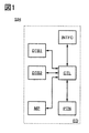
- FIG. 1 is a block diagram showing a configuration example of the system.
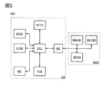
- FIG. 2 is a block diagram showing a configuration example of the system.
- FIG. 3 is a flowchart showing an operation example of the system.
- FIG. 4 is a flowchart showing an operation example of the system.
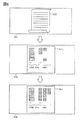
- FIG. 5 is a diagram illustrating a procedure for creating a netlist from a circuit diagram.
- FIG. 6 is a diagram illustrating a procedure for creating a netlist from a document file.
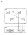
- FIG. 7 is a block diagram illustrating an operation example of the system.
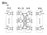
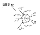
- 8A and 8B are diagrams illustrating a hierarchical neural network.
- FIG. 9 is a block diagram showing a configuration example of an arithmetic circuit.
- FIG. 9 is a block diagram showing a configuration example of an arithmetic circuit.
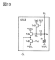
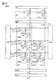
- FIG. 10 is a circuit diagram showing a configuration example of a circuit included in the arithmetic circuit.
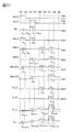
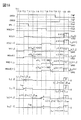
- FIG. 11 is a timing chart showing an operation example of the arithmetic circuit.
- FIG. 12 is a block diagram showing a configuration example of an arithmetic circuit.
- FIG. 13 is a circuit diagram showing a configuration example of an arithmetic circuit.
- FIG. 14 is a circuit diagram showing a configuration example of an arithmetic circuit.
- FIG. 15 is a circuit diagram showing a configuration example of an arithmetic circuit.
- FIG. 16 is a circuit diagram showing an example of an equivalent circuit of the arithmetic circuit of FIG.
- FIG. 17 is a block diagram showing a configuration example of an arithmetic circuit.
- FIG. 18 is a timing chart showing an operation example of the arithmetic circuit.
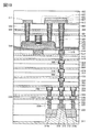
- FIG. 19 is a schematic cross-sectional view illustrating the configuration of the semiconductor device.
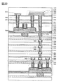
- FIG. 20 is a schematic cross-sectional view illustrating the configuration of the semiconductor device.
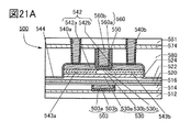
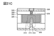
- 21A to 21C are schematic cross-sectional views for explaining the configuration of the semiconductor device.
- 22A and 22B are schematic cross-sectional views illustrating a configuration example of the transistor.
- FIG. 23 is a schematic cross-sectional view illustrating a configuration example of the semiconductor device.
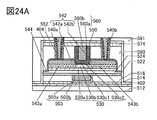
- 24A and 24B are schematic cross-sectional views illustrating a configuration example of the transistor.
- FIG. 25 is a schematic cross-sectional view illustrating a configuration example of the semiconductor device.
- FIG. 25 is a schematic cross-sectional view illustrating a configuration example of the semiconductor device.
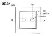
- FIGS. 26B and 26C are cross-sectional perspective views showing a configuration example of the capacitance.
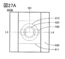
- 27A is a top view showing a configuration example of the capacitance
- FIG. 27B is a cross-sectional view showing a configuration example of the capacitance
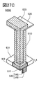
- FIG. 27C is a sectional perspective view showing a configuration example of the capacitance.
- 28A is a diagram for explaining the classification of the crystal structure of IGZO
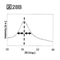
- FIG. 28B is a diagram for explaining the XRD spectrum of quartz glass
- FIG. 28C is a diagram for explaining the XRD spectrum of crystalline IGZO
- FIG. 28D is a diagram for explaining the XRD spectrum of crystalline IGZO. It is a figure explaining the microelectron diffraction pattern of a crystalline IGZO.
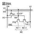
- FIG. 29A is a circuit diagram showing a configuration of a multiplication circuit included in the prototype semiconductor device
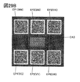
- FIG. 29B is an optical micrograph of the prototype semiconductor device.
- Figure 30A writes data corresponding to V W to a multiplier circuit included in the semiconductor device trial, the multiplying circuit the source of the transistor M2 in the case of applying the voltage V X to the wiring VX - drain current I DS ( It is a graph which shows V W , V X ), and
- FIG. 30B is a graph which shows the multiplication characteristic of the multiplication circuit included in the prototype semiconductor device calculated from FIG.
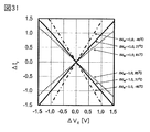
- FIG. 31 is a graph showing the temperature dependence of the multiplication characteristics of the multiplication circuit included in the prototype semiconductor device.
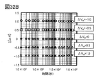
- 32A and 32B are graphs showing the time change of the multiplication characteristics of the multiplication circuit included in the prototype semiconductor device.
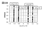
- FIG. 33A is a graph showing the multiplication characteristics of the multiplication circuit included in the prototype semiconductor device, and FIG. 33B is the multiplication when each potential is written to the multiplication circuit included in the prototype semiconductor device. It is a graph which showed the degree of variation of a characteristic.
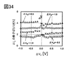
- FIG. 34 is a graph showing the degree of element variation of the read current of each of the plurality of multiplication circuits included in the prototype semiconductor device.
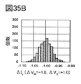
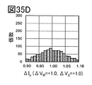
- 35A, 35B, 35C, and 35D are graphs showing the degree of element variation of the read current in the configuration of a plurality of multiplication circuits obtained by Monte Carlo analysis.
- FIG. 36 is a diagram showing an example of a model of a hierarchical artificial neural network used for calculating the inference accuracy.
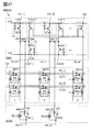
- FIG. 37 is a circuit diagram illustrating a configuration example of the semiconductor device.
- FIG. 38A is a graph showing the result of the product of the first data and the second data
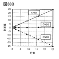
- FIG. 38B is a graph showing the calculated values according to the number of rows in the memory cell array.
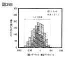
- 39A and 39B are histograms showing the variation in the value of the product of the first data and the second data when the variation in the characteristics of the transistor is taken into consideration.
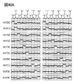
- FIG. 40A is a graph showing the degree of coincidence output from each output layer of the neural network configured by the circuit simulator and the neural network configured by the programming language
- FIG. 40B is the neural network configured by the circuit simulator. It is a graph which shows the correlation of the value output from each output layer of a network and a neural network constructed by a programming language.
- FIG. 41 shows an example of the output waveform from the output layer in the neural network configured by the circuit simulator.
- the synaptic connection strength can be changed by giving existing information to the neural network.
- the process of giving existing information to the neural network and determining the bond strength may be called "learning”.
- Examples of the neural network model include a Hopfield type and a hierarchical type.
- a neural network having a multi-layer structure may be referred to as a “deep neural network” (DNN), and machine learning by a deep neural network may be referred to as “deep learning”.
- DNN deep neural network
- a metal oxide is a metal oxide in a broad sense. Metal oxides are classified into oxide insulators, oxide conductors (including transparent oxide conductors), oxide semiconductors (also referred to as Oxide Semiconductor or simply OS) and the like.
- the metal oxide when a metal oxide is used in the active layer of a transistor, the metal oxide may be referred to as an oxide semiconductor. That is, when a metal oxide can form a channel forming region of a transistor having at least one of an amplification action, a rectifying action, and a switching action, the metal oxide is referred to as a metal oxide semiconductor, abbreviated as a metal oxide semiconductor. It can be called an OS. Further, when describing as an OS FET or an OS transistor, it can be paraphrased as a transistor having a metal oxide or an oxide semiconductor.
- a metal oxide having nitrogen may also be collectively referred to as a metal oxide. Further, a metal oxide having nitrogen may be referred to as a metal oxynitride.
- each embodiment shall be appropriately combined with the configuration shown in other embodiments (or other examples) to form one aspect of the present invention. Can be done. Further, when a plurality of configuration examples are shown in one embodiment, the configuration examples can be appropriately combined with each other.
- the content may be a part of the content described in one embodiment (or an embodiment) may be another content (a part of the content) described in the embodiment (or the embodiment). ) And the content (may be a part of the content) described in one or more other embodiments (or one or more other embodiments). Alternatively, it can be replaced.
- the content described in the embodiment means the content described by using various figures in each embodiment (or the embodiment), or the text described in the specification. This is what is stated.
- the figure (may be a part) described in one embodiment (or an embodiment) is another part of the figure, another figure (or a part thereof) described in the embodiment (or the embodiment).
- Many figures can be constructed.
- FIG. 1 is a system (sometimes referred to as an electronic device) having a function of converting a “circuit drawing”, a “circuit configuration described in the claims”, etc. in AI using a neural network into a netlist. ) Is shown. In addition, the system has a function of searching in an existing database using the converted netlist.
- a netlist has connection information of circuit elements, logic circuits, signal conversion circuits, potential level conversion circuits, voltage sources, current sources, switching circuits, amplification circuits, etc. included in the electronic circuits in electronic circuits and the like. It is data. Specifically, the netlist is data in which the connection destinations of the terminals of the circuit elements and circuits included in the electronic circuit are described, and is used in a circuit simulator, circuit design software, and the like.
- the system SIH shown in FIG. 1 has an electronic device ED.
- the electronic device ED has an input / output interface INTFC, a control unit CTL, a conversion unit PTN, a database DTB1, a database DTB2, and a storage unit MP.
- the input / output interface INTFC is electrically connected to the control unit CTL.
- the input / output interface INTFC has a function of inputting / outputting information between the user and the electronic device ED when the user uses the system SIH.
- Examples of the input / output interface INTFC include hardware such as an organic EL (Electro Luminescence) display, a display device such as a liquid crystal display, a keyboard, and a pointing device (for example, a mouse). Further, the display device may have an input device such as a touch panel.
- the storage unit MP is electrically connected to the control unit CTL.
- the storage unit MP includes a volatile storage device, a non-volatile storage device, and the like.
- Examples of the volatile storage device include DRAM (Dynamic Random Access Memory) and the like.
- the volatile storage device has a function of temporarily storing data necessary for the process of calculation or during the startup of software, for example.
- non-volatile storage device examples include HDD (hard disk drive), SSD (solid state drive), optical disk, magnetic tape, and the like.
- HDD hard disk drive
- SSD solid state drive
- optical disk magnetic tape
- the non-volatile storage device has a function of storing, for example, a software execution program, a drawing in which a circuit configuration is drawn, a netlist of circuit configurations, and the like.
- the conversion unit PTN is electrically connected to the control unit CTL.
- the conversion unit PTN has a function of converting a circuit diagram, a document file expressing a circuit in sentences (for example, the scope of claims of a patent specification, etc.) into a netlist.
- the conversion unit PTN may be, for example, an arithmetic circuit constituting a neural network. Further, when a neural network is configured in the conversion unit PTN, it is assumed that the neural network has already been learned and the weighting coefficients of the neurons included in the neural network are fixed.
- the database DTB1 is electrically connected to the control unit CTL.
- the database DTB1 has a function of storing document data such as patent specifications, papers, and materials.
- the database DTB2 is electrically connected to the control unit CTL.
- the database DTB2 has, for example, a function of storing a netlist of circuits described in the literature data stored in the database DTB1.
- the netlist may include a control number, a control symbol, and the like for associating the netlist with the circuit configuration of the document data.
- database DTB1 and the database DTB2 may be combined as one database.
- the database DTB1 and the database DTB2 store the document data and the netlist as described above, the database DTB1 and the database DTB2 may be included in the storage unit MP.
- the database DTB1 and the database DTB2 are preferably non-volatile storage devices of the storage unit MP.
- the electronic device ED may have an external interface INF.
- the external interface INF has a function of communicating with the electronic device WSV outside the electronic device ED. Therefore, the external interface INF is electrically connected to the control unit CTL and the electronic device WSV.
- the electronic device WSV can be, for example, an external server. Therefore, it is preferable that the external interface INF is connected to the electronic device WSV by an internet line or the like.
- the electronic device WSV has, for example, a database WDTB1, a database WDTB2, and a conversion unit WPTN. Similar to the database DTB1, the database WDTB1 stores literature data. Further, in the database WDTB2, as in the database DTB2, a netlist of circuits and the like described in the literature data of the database WDTB1 are stored. Similar to the conversion unit PTN, the conversion unit WPTN has a function of converting a circuit diagram, a document file expressing a circuit in sentences, and the like into a netlist.
- At least one of the database WDTB1, the database WDTB2, and the conversion unit WPTN may function as an external server.
- the scale, storage capacity, computing power, and the like of the provided server may be increased.
- the database WDTB1 may be able to store more document data than the database DTB1.
- the database WDTB2 may be able to store more information such as a netlist than the database DTB2.
- the conversion unit WPTN may have an arithmetic circuit having a larger scale than the conversion unit PTN.
- FIG. 3 is a flowchart showing an operation example of the system SIH, and the operation example of the system SIH has steps STI01 to STI03. Further, in FIG. 3, the start of the operation example is described as "START”, and the end of the operation example is described as "END". In this operation example, an operation of converting a circuit diagram or a document file expressing a circuit in sentences into a netlist will be described.
- Step STI01 has a step in which the user inputs a circuit diagram or a document file expressing the circuit in sentences to the control unit CTL of the electronic device ED using the input / output interface INTFC.
- the means for inputting the circuit diagram by the user include means for creating a circuit diagram using circuit design software, a circuit simulator, paint software, CAD software, and the like.
- a means for inputting the document file by the user a means for creating a document file by using a document creation software, a text editor, or the like can be mentioned.
- the circuit diagram and the document file in the process of being created, the created circuit diagram, the document file and the like may be temporarily saved in the storage unit MP.
- the circuit diagram or document file created in step STI01 is referred to as input data.
- step STI01 as the input data, a circuit diagram, a document file, or the like read from the database DTB1 may be applied in addition to the created data.
- Step STI02 has a step of converting the input data created in step STI01 into a netlist by the conversion unit PTN.
- the user uses the input / output interface INTFC to transmit input data and a signal including an instruction to convert the input data into a netlist to the control unit CTL.
- the control unit CTL receives the input data and the signal, and transmits the input data to the conversion unit PTN.
- the conversion unit PTN converts the input data into a netlist by receiving the input data.
- a method using, for example, a convolutional neural network (CNN) is preferable as a method for converting the input data into a netlist.
- CNN convolutional neural network
- the input data is a document file
- a method using, for example, a recursive neural network is preferable as a method for converting the input data or the like into a netlist. A specific example of the method of converting the input data to the netlist will be described later.
- converted netlist may be temporarily saved in the storage unit MP.
- Step STI03 has a step of outputting the netlist converted in step STI02 to a display device or the like included in the input / output interface INTFC. Specifically, for example, the netlist converted in step STI02 is transmitted to a display device included in the input / output interface INTFC via the control unit CTL. After that, by displaying the netlist on the display device or the like, the user can confirm the contents of the netlist converted from the input data.
- step STI03 After step STI03 is performed, this operation ends.
- FIG. 4 is a flowchart showing an operation example of the system SIH, and the flowchart is an operation example in which steps STI04 to STI08 are further added to the operation example of FIG. In this operation example, a method of searching for a circuit using the converted netlist will be described.
- steps STI01 to STI03 shown in the flowchart of FIG. 4 the description of steps STI01 to STI03 of the flowchart of FIG. 3 is taken into consideration.
- Step STI04 has a step of searching the database DTB2 for a circuit using the netlist converted in step STI02. Specifically, for example, the control unit CTL transmits a signal to the database DTB2 including a command for reading the netlist associated with the document data stored in the database DTB2. Then, the database DTB2 reads the netlist by receiving the signal and transmits it to the control unit CTL, and the control unit CTL includes the netlist converted in step STI02 and the netlist included in the database DTB2. Make a comparison.
- the netlist linked to the literature data from the database DTB2 may be read from all the netlists stored in the database DTB2, or may be conditionally stored in the database DTB2. You may narrow down to the netlist of the department.
- step STI04 those that completely match the netlist converted in step STI02 may be extracted, or those that partially match (similar ones) may be extracted.
- the converted netlist used for the search may be temporarily saved in the storage unit MP.
- AI may be used for the circuit search performed in step STI04. Specifically, for example, using AI, the descriptions of the netlist converted in step STI02 and the netlist associated with the literature data stored in the database DTB2 are compared, and each other is compared. In the netlist, the similarity indicating how much the types, numbers, connection configurations, etc. of the circuit elements match may be calculated, and the search results may be output from the one with the highest similarity.
- Step STI05 has a step of determining whether or not the netlist converted in step STI02 is found in the database DTB2 in the search of step STI04.
- the netlist found in the database DTB2 referred to here includes a case where it completely matches the netlist searched in step STI04 and a case where it partially matches. In the determination, when the netlist searched in step STI04 is found in the database DTB2, this operation shifts to step STI06. Further, in the determination, when the netlist searched in step STI04 is not found in the database DTB2, this operation shifts to step STI07.
- Step STI06 has a step of reading the document data corresponding to the netlist found in the database DTB2 in the search of step STI04 from the database DTB1.
- the control unit CTL transmits a signal to the database DTB1 including a command for reading the document data corresponding to the netlist read from the database DTB2, which is caught in the search in step STI04.
- the database DTB1 reads out the document data and transmits it to the control unit CTL.
- the control unit CTL transmits the document data to a display device or the like included in the input / output interface INTFC. After that, by displaying the document data on the display device or the like, the user can confirm the contents of the document data.
- converted netlist used for the search and the document data read from the database DTB1 may be temporarily stored in the storage unit MP.
- step ST106 After step ST106 is performed, this operation ends.
- Step STI07 has a step of outputting the result that the netlist converted in step STI02 was not found in the database DTB2 in the search of step STI04.
- the control unit CTL transmits information to the input / output interface INTFC that the netlist converted in step STI02 was not found in the database DTB2.
- the user can confirm the search result that the netlist converted in step STI02 was not found in the database DTB2.
- Step STI08 has a step of storing the input data in the database DTB1 and storing the netlist converted in step STI02 in the database DTB2.
- the user uses the input / output interface INTFC to transmit a signal including an instruction for storing the input data and the netlist converted in step STI02 to the control unit CTL.
- the control unit CTL Upon receiving the signal, the control unit CTL transmits the input data and the signal including the instruction to write the input data to the database DTB1 to the database DTB1, and the netlist converted in step STI02 and the netlist. Is transmitted to the database DTB2 with a signal including an instruction to write to the database DTB2.
- the input data transmitted to the database DTB1 and the converted netlist transmitted to the database DTB2 are transmitted from the storage unit MP in which they are temporarily stored via the control unit CTL. May be good.
- step STI08 After step STI08 is performed, this operation ends.
- the operation method of one aspect of the present invention is not limited to the above-mentioned steps STI01 to STI08.
- the processes shown in the flowchart are classified according to functions and shown as steps independent of each other.
- one step may involve a plurality of steps, or one step may be involved over a plurality of steps. Therefore, the processing shown in the flowchart is not limited to each step described in the specification, and can be appropriately replaced depending on the situation.
- the order of steps can be changed, steps can be added, deleted, and the like, depending on the situation, in some cases, or as necessary.
- step STI08 may be deleted from this operation example and may not be performed if the user does not want it.
- the operation method of one aspect of the present invention is not limited to the operation example described in the present embodiment.
- an operation example of converting input data to a netlist using the conversion unit PTN of the electronic device ED has been described, but the conversion unit PTN of the electronic device WSV may be used instead.
- an operation example of searching the circuit of the netlist using the database DTB1 and the database DTB2 of the electronic device ED has been described, but the database DTB1 and the database DTB2 are instead used as the database WDTB1 and the database of the electronic device WSV.
- WDTB2 may be used.
- a service for converting input data to a netlist using an electronic device ED and an external electronic device WSV, and / or a circuit search service using the netlist, etc. are charged.
- the business model may be provided.
- step STI02 of the above operation example when the input data is used as a circuit diagram, a method for converting the circuit diagram into a netlist will be described.
- FIG. 5 is a schematic diagram showing the flow of converting a circuit diagram to a netlist.
- Step PH1 in FIG. 5 shows an example of an image as input data to be input to the conversion unit PTN in step STI02.
- a circuit diagram is drawn on the image PIC, and the circuit diagram shows circuit symbols, wiring, and their connection configurations. Further, in some cases, as shown in the image PIC of FIG. 5, the image PIC may include a name of a circuit symbol, a character indicating a name of wiring, a code, and the like. Further, the circuit diagram shown in the image PIC of FIG. 5 may not include the names of circuit symbols, characters indicating wiring names, symbols, and the like.
- the step PH2 in FIG. 5 shows an example in which the image PIC of the step PH1 is input to the conversion unit PTN and the object region is recognized by the image PIC.
- the image PIC on the left side of the stage PH2 in FIG. 5 the circuit symbol and the electrical connection part (corresponding to the black circle in the circuit diagram shown in the image PIC) are recognized and each is surrounded by a dotted line. Is shown. Further, depending on the situation, the recognition of the object area may be performed including wiring.
- Examples of the method for recognizing the object region shown above include Objectness, CPMC (Constralined Parametric Min-Cuts), and Object Proposals.
- the conversion unit PTN can be made to recognize what kind of circuit element the circuit symbol surrounded by the dotted line is. For example, by performing image recognition in the image PIC on the left side of the step PH2 in FIG. 5, the conversion unit PTN recognizes, for example, the circuit symbol surrounded by the thick broken line as a capacitive element, and for example, the thick one-dot chain line.
- the circuit symbol surrounded by can be recognized as a transistor.
- the conversion unit PTN can give the circuit symbol a name (for example, a character, an abbreviation, a code, a word, etc.) to be described in the netlist. it can.
- the conversion unit PTN can recognize the electrical connection portion (black circle, etc.) surrounded by the dotted line. As a result, the conversion unit PTN can give a name (for example, a character, an abbreviation, a code, a word, etc.) to be described in the netlist to the electrical connection portion (black circle, etc.).
- a name for example, a character, an abbreviation, a code, a word, etc.
- a method of extracting the circuit symbols included in the image PIC based on the learned circuit symbols can be mentioned.
- a convolutional neural network (CNN) or the like can be used as a method of performing image recognition.
- CNN convolutional neural network
- an image of a circuit symbol, an image of an electrical connection portion (black circle, etc.), and a part of those images may be used in advance as a filter of the convolutional layer of the convolutional neural network.
- the similarity between the circuit symbol, the electrical connection part (black circle, etc.) included in the image PIC and the filter can be calculated by the calculation by the convolutional neural network, and from the similarity.
- the circuit symbol included in the image PIC, the electrical connection part (black circle, etc.) and the like can be identified.
- the conversion unit PTN recognizes the connection between the electrical connection portion (black circle or the like) and the circuit symbol
- the first image recognition it is determined in which direction the wiring connected to the electrical connection portion (black circle, etc.) is extended, and in the second recognition of the object area, the extension is made. The area is expanded in the direction of, and the wiring and the electrical connection part (black circle, etc.) are collectively recognized as an object area.
- the conversion unit PTN can recognize the wiring connected to the electrical connection portion (black circle, etc.) according to the number of repetitions of the recognition of the object area and the image recognition, and finally.
- the conversion unit PTN can recognize the electrical connection between the circuit symbol and the electrical connection portion (black circle, etc.).
- the image PIC on the left side of the stage PH2 in FIG. 5 shows, as an example, a region surrounded by a thick two-dot chain line as a wiring region obtained by repeatedly recognizing an object region and image recognition. ..
- the recognition may be performed together with the circuit symbol and the electrical connection part at the stage of recognizing the object area.
- the names, characters, codes, etc. acquired by recognizing the object area can be associated with the circuit symbol and the electrical connection portion that also recognize the object area.
- circuit symbols, names associated with electrical connection parts, characters, codes, etc. can be treated as symbols, characters, etc. described in the netlist.
- stage PH3 of FIG. 5 an example is shown in which the connection configuration of the circuit symbol recognized by the conversion unit PTN and the electrical connection portion (black circle, etc.) is described in the netlist in the stage PH2 of FIG.
- the circuit symbol recognized by the image PIC is described as the name CSW of the circuit element (for example, letters, abbreviations, symbols, words, etc.).
- Tr [1] and Tr [2] indicate transistors in the circuit diagram drawn in the image PIC
- C [1] indicates the capacitive elements in the circuit diagram drawn in the image PIC
- EL [1]. 1] shows the light emitting element of the circuit diagram drawn in the image PIC.
- the name CNP for example, a character, etc.
- the electrical connection portion black circle, etc.
- the space SPC space SPC.
- abbreviations, symbols, words, etc. are listed.
- a space is provided between the names CNPs.
- the order in which the names CNP of the electrical connection portions (black circles, etc.) are described is determined by the terminals of the circuit symbols of the names CSW described in the column.
- the netlist NTL stipulates that the electrical connection of each terminal of a transistor is described in the order of one of the source or drain, the other of the gate, source or drain. Further, for example, in the netlist NTL, it is defined that the electrical connection of each terminal of the light emitting element is described in the order of the input terminal and the output terminal.
- the circuit diagram as input data can be converted into a netlist by recognizing the object area and recognizing the image.
- step STI02 of the above operation example when the input data is a document file or the like, a method for converting the circuit diagram into a netlist will be described.
- FIG. 6 is a schematic diagram showing the flow of converting a document file to a netlist.
- Step PH4 in FIG. 6 shows an example of a document file to be input data input to the conversion unit PTN in step STI02.
- the circuit configuration is described as a sentence as information for converting to a netlist using the conversion unit PTN.
- the document file DOC that expresses the circuit configuration as a sentence can be, for example, a description of the circuit described in the patent specification, a scope of claims attached to the patent specification, or the like. As an example of the conversion method here, it is assumed that the document file DOC contains the sentences as shown in Table 1 below.
- the conversion unit PTN When the above-mentioned document file DOC is input as input data, the conversion unit PTN performs text analysis on the document file DOC as an example.
- a document file for example, a dissertation, a scope of claims described in a patent publication, etc.
- its claim are given to the conversion unit PTN in advance as teacher data. It is preferable to train the netlist corresponding to the document file.
- the document file can be converted into a netlist based on the learned contents.
- a plurality of document files for example, a plurality of "claims" having the same contents but different descriptions" from one netlist. Etc.
- a plurality of document files for example, a plurality of "claims" having the same contents but different descriptions" from one netlist. Etc.
- a recurrent neural network (RNN) or the like can be used as a method of performing text analysis.
- RNN recurrent neural network
- the conversion unit PTN can recognize the circuit element, wiring, or electrical connection point from the circuit configuration shown in the document file DOC. For example, by performing text analysis on the text in the first paragraph of the document file DOC, the conversion unit PTN has the first transistor, the second transistor, and the circuit configuration shown in the document file DOC. It can be recognized that the capacitive element and the light emitting element are included. Subsequently, for example, by performing text analysis on each sentence of the second paragraph, the third paragraph, the fifth paragraph, and the seventh paragraph, the conversion unit PTN has the circuit configuration shown in the document file DOC. It can be recognized that the signal line, the scanning line, the first power supply line, and the second power supply line are electrically connected to the above.
- the conversion unit PTN uses the name CSW (for example, letters, abbreviations, symbols, words, etc.) of the circuit element as, for example, Tr [1] for the first transistor, Tr [2] for the second transistor, and capacitance.
- the element is named C [1]
- the light emitting element is named EL [1]
- the name of the electrical connection point is CNP (for example, a letter, an abbreviation, a code, a word, etc.), and the signal line, scanning line, first.
- the conversion unit PTN can describe a more detailed netlist NTL. For example, by performing text analysis on the sentences in the 4th and 8th paragraphs of the document file DOC, the conversion unit PTN can use the source of the first transistor, the gate of the second transistor, and the capacitive element. It can be recognized that one of the pair of electrodes is connected to the same electrical connection point. Here, the conversion unit PTN names the electrical connection point N3.
- the conversion unit PTN has the source of the second transistor, the input terminal of the light emitting element, and the pair of capacitive elements. It can be recognized that the other of the electrodes of is connected to the same electrical connection point.
- the conversion unit PTN shall name the electrical connection point N4.
- the conversion is performed by performing a text analysis on the document file DOC, determining the circuit elements included in the circuit configuration described in the document file DOC, and extracting their electrical connections.
- the part PTN can describe the netlist NTL illustrated in step PH6 of FIG.
- the database DTB1 stores the information PKEDD, the information PKPD, the information HSCD, and the information HSPD
- the database DTB2 contains the netlist PKEDN.
- the netlist PKPN, the netlist HSCN, and the netlist HSPN are stored (however, in FIG. 7, the input / output interface INTFC, the control unit CTL, the conversion unit PTN, and the storage unit MP are omitted. ing).
- the information PKEDD has, for example, a circuit diagram, specifications, etc. of a known electronic device
- the information PKPD is, for example, a technical content (patent specification, particularly patent drawing, claims, etc.) in which a person other than the user is involved.
- the information HSCD has, for example, the scope of claims for the circuit of the patent specification (whether or not there is an application) with which the user is involved, and the information HSPD has, for example, the user.
- the netlist PKEDN has a netlist corresponding to the circuit diagram included in the information PKEDD
- the netlist PKPN has a netlist corresponding to the patent drawings, the scope of patent claims, etc. included in the information PKPD
- the netlist HSCN has a netlist corresponding to the scope of patent claims included in the information HSCD
- the netlist HSPN has a netlist corresponding to the patent drawings included in the information HSPD.
- FIG. 7 as an expression of the association between the netlist and the information, between the netlist PKEDN and the information PKEDD, between the netlist PKPN and the information PKPD, between the netlist HSCN and the information HSCD, and the net.
- a thick solid line is drawn between the list HSPN and the information HSPD.
- the first search SRC1 one netlist PKEDN corresponding to the circuit diagram of a known electronic device is used as the search range, and a plurality of netlist HSCNs such as the claims of the patent application in which the user is involved are used as the search range.
- searching the filing date of the patent corresponding to the found netlist was earlier than the date when the netlist corresponding to the netlist PKEDN was found from the plurality of netlist HSCNs and the electronic device became publicly known. If so, a conflict with the user's patent by the electronic device can be found. That is, by performing the first search SRC1, it is possible to search for a conflict of patents of a user with a known electronic device.
- the second search SRC2 one netlist HSCN of the claims before filing a patent application involving the user, a plurality of netlist PKEDN corresponding to a circuit diagram of a known electronic device, and other than the user.
- a netlist corresponding to the netlist HSCN is found from the plurality of netlist PKEDN and the plurality of netlist PKPN, it can be determined that the netlist HSCN is known. That is, by performing the second search SRC2, it is possible to search for the novelty of the invention in which the user is involved before filing a patent application. As a result, the patent validity of the patent application involving the user may be enhanced.
- the third search SRC3 there is a case where one netlist PKEDN corresponding to a circuit diagram of a known electronic device is searched using a plurality of netlist HSPNs such as drawings of patent applications in which the user is involved as a search range. Think. At this time, the filing date of the patent corresponding to the found netlist was earlier than the date when the netlist corresponding to the netlist PKEDN was found from the plurality of netlist HSPNs and the electronic device became publicly known. In this case, it can be said that the electronic device may utilize the contents of the patent application in which the user was involved. That is, by performing the third search SRC3, it is possible to check the degree of similarity between the circuit diagram of the known electronic device and the circuit diagram of the content of the patent application in which the user is involved.
- the third search SRC3 one netlist PKEDN corresponding to the circuit diagram of a known electronic device is searched, and a plurality of netlist HSPNs such as drawings of patent applications in which the user is involved are searched as a search range.
- the third search SRC3 searches one netlist HSPN such as a drawing of a patent application involved by a user with a plurality of netlist PKEDNs corresponding to circuit diagrams of known electronic devices as a search range. You may. Also in this search, the degree of similarity between the circuit diagram of a known electronic device and the circuit diagram of the content of the patent application involved by the user can be examined.
- first search SRC1 and the third search SRC3 may be performed at the same time.
- AI can be used for each of the first search SRC1, the second search SRC2, and the third search SRC3. For example, by using AI, the descriptions of the netlist to be searched and the netlist included in the search range are compared, and in each netlist, the type, number, connection configuration, etc. of circuit elements, etc. It is possible to calculate the similarity indicating how much the two match, and output the search result from the one with the highest similarity.
- each of the information PKEDD, the information PKPD, the information HSCD, and the information HSPD stored in the database DTB1 is associated with the netlist stored in the database DTB2.
- each of the first search SRC1, the second search SRC2, and the third search SRC3 can perform a search without converting the netlist into another file (for example, a circuit diagram, a document file, etc.). Therefore, the search can be facilitated and the search speed can be increased.
- a large amount of data (sometimes called big data) is required.
- a program that automatically and randomly generates a netlist is created, and then image data is created from the netlist using circuit design software, a circuit simulator, or the like.
- it is preferable to build a program so that the generation of the netlist and the creation of the image data can be performed in a series.
- a set of the netlist and the image data of the circuit can be prepared as data for learning.
- a program that automatically and randomly generates a netlist is created, and further, a program that creates a document file from the automatically generated netlist is created.
- a set of a netlist and a document file can be prepared as learning data.
- a hierarchical neural network has one input layer, one or more intermediate layers (hidden layers), and one output layer, and is composed of a total of three or more layers.
- the hierarchical neural network 100 shown in FIG. 8A shows an example thereof, and the neural network 100 has a first layer to an R layer (R here can be an integer of 4 or more). ing.
- R can be an integer of 4 or more
- the first layer corresponds to the input layer
- the R layer corresponds to the output layer
- the other layers correspond to the intermediate layer.
- FIG. 8A shows the (k-1) th layer and the kth layer (k here is an integer of 3 or more and R-1 or less) as the intermediate layer, and the other intermediate layers. Is not shown.
- Each layer of the neural network 100 has one or more neurons.
- the first layer has neurons N 1 (1) to neurons N p (1) (where p is an integer of 1 or more), and the layer (k-1) is neuron N 1. (K-1) to neuron N m (k-1) (where m is an integer of 1 or more), and the k-th layer has neurons N 1 (k) to neurons N n (k) (
- n is an integer of 1 or more
- the R layer has neurons N 1 (R) to neurons N q (R) (q here is an integer of 1 or more).
- FIG. 8B is a neuron N j of the k-th layer (k), shows the signal which is input to the neuron N j (k), a signal output from the neuron N j (k), the.
- z 1 (k-1) to z m (k- ), which are output signals of neurons N 1 (k-1) to N m (k-1) in the (k-1) layer , respectively. 1) is output toward the neuron Nj (k) .
- the neuron N j (k) is, z 1 (k-1) to z m (k-1) to generate a z j (k) in response to, the z j (k) is an output signal (k + 1 ) Output to each neuron in the layer (not shown).
- the degree of signal transmission of signals input from neurons in the previous layer to neurons in the next layer is determined by the strength of synaptic connections (hereinafter referred to as weighting factors) that connect these neurons.
- weighting factors the strength of synaptic connections that connect these neurons.
- the signal output from the neurons in the previous layer is multiplied by the corresponding weighting factor and input to the neurons in the next layer.
- i an integer 1 or m
- the signal input to the neuron Nj (k) in the kth layer can be expressed by the equation (D1).
- the result of the sum of products may be biased as a bias.
- the equation (D2) can be rewritten as the following equation.
- the neuron N j (k) produces an output signal z j (k) in response to u j (k) .
- the output signal z j (k) from the neuron N j (k) is defined by the following equation.
- the function f (u j (k) ) is an activation function in a hierarchical neural network, and a step function, a linear ramp function, a sigmoid function, or the like can be used.
- the activation function may be the same or different in all neurons.
- the activation function of neurons may be the same or different in each layer.
- the signal output by the neurons in each layer, the weighting coefficient w, or the bias b may be an analog value or a digital value.
- the digital value may be, for example, a binary value or a ternary value. A value with a larger number of bits may be used.
- an analog value for example, a linear ramp function, a sigmoid function, or the like may be used as the activation function.
- binary digital values for example, a step function with an output of -1 or 1 or 0 or 1 may be used.
- the signal output by the neurons in each layer may have three or more values.
- the activation function has three or more values, for example, a step function having an output of -1, 0, or 1, or 0, 1, or.
- a step function or the like set to 2 may be used.
- a step function of -2, -1, 0, 1, or 2 may be used.
- the neural network 100 When the input signal is input to the first layer (input layer), the neural network 100 is sequentially input from the front layer in each layer from the first layer (input layer) to the last layer (output layer). Based on the signal, an output signal is generated using the equation (D1), the equation (D2) (or the equation (D3)), and the equation (D4), and the output signal is output to the next layer.
- the signal output from the last layer (output layer) corresponds to the result calculated by the neural network 100.
- FIG. 9 shows a configuration example of the arithmetic circuit MAC1.
- the arithmetic circuit MAC1 shown in FIG. 9 performs a product-sum operation of the first data held in the memory cell described later and the input second data, and activates the activation function using the result of the product-sum operation. It is a circuit that performs the calculation of.
- the first data and the second data can be analog data or multi-valued data (discrete data) as an example.
- the arithmetic circuit MAC1 has a current source circuit CS, a current mirror circuit CM, a circuit WDD, a circuit WLD, a circuit CLD, a circuit OFST, an activation function circuit ACTV, and a memory cell array CA.
- the memory cell array CA has a memory cell AM [1], a memory cell AM [2], a memory cell AMref [1], and a memory cell AMref [2].
- the memory cell AM [1] and the memory cell AM [2] have a role of holding the first data, and the memory cell AMref [1] and the memory cell AMref [2] are used to perform the product-sum operation. It has a function to hold the required reference data.
- the reference data can be analog data or multi-valued data (discrete data) as well as the first data and the second data.
- the memory cell array CA of FIG. 9 two memory cells are arranged in the row direction and two in the column direction in a matrix, whereas in the memory cell array CA, three or more memory cells are arranged in the row direction and columns. Three or more in the direction may be arranged in a matrix. Further, when multiplication is performed instead of the multiply-accumulate operation, the memory cell array CA may have one memory cell in the row direction and two or more memory cells in the column direction arranged in a matrix.
- the memory cell AM [1], the memory cell AM [2], the memory cell AMref [1], and the memory cell AMref [2] have a transistor Tr11, a transistor Tr12, and a capacitance C1, respectively.
- the transistor Tr11 is preferably an OS transistor.
- the channel formation region of the transistor Tr11 is indium, element M (element M includes, for example, aluminum, gallium, yttrium, copper, vanadium, beryllium, boron, titanium, iron, nickel, germanium, zirconium, molybdenum, lantern. , One or more selected from cerium, neodymium, hafnium, tantalum, tungsten, gallium and the like.), It is more preferable that the oxide contains at least one of zinc. It is more preferable that the transistor Tr11 has the structure of the transistor described in the third embodiment.
- the leakage current of the transistor Tr11 can be suppressed, so that a product-sum calculation circuit with high calculation accuracy may be realized. Further, by using the OS transistor as the transistor Tr11, the leakage current from the holding node to the writing word line in the non-conducting state of the transistor Tr11 can be made very small. That is, since the potential refresh operation of the holding node can be reduced, the power consumption of the product-sum calculation circuit can be reduced.
- the transistor Tr12 can be manufactured at the same time as the transistor Tr11 by using the OS transistor, the manufacturing process of the product-sum calculation circuit may be shortened. Further, the channel forming region of the transistor Tr12 may contain silicon instead of oxide.
- the silicon may be, for example, amorphous silicon (sometimes called hydrogenated amorphous silicon), microcrystalline silicon, polycrystalline silicon, single crystal silicon, or the like.
- the first terminal of the transistor Tr11 is the gate of the transistor Tr12 and electricity. Is connected.
- the first terminal of the transistor Tr12 is electrically connected to the wiring VR.
- the first terminal of the capacitance C1 is electrically connected to the gate of the transistor Tr12.
- the second terminal of the transistor Tr11 is electrically connected to the wiring WD, and the gate of the transistor Tr11 is electrically connected to the wiring WL [1].
- the second terminal of the transistor Tr12 is electrically connected to the wiring BL, and the second terminal of the capacitance C1 is electrically connected to the wiring CL [1].
- the connection point between the first terminal of the transistor Tr11, the gate of the transistor Tr12, and the first terminal of the capacitance C1 is a node NM [1].
- the current flowing from the wiring BL to the second terminal of the transistor Tr12 is defined as I AM [1] .
- the second terminal of the transistor Tr11 is electrically connected to the wiring WD, and the gate of the transistor Tr11 is electrically connected to the wiring WL [2].
- the second terminal of the transistor Tr12 is electrically connected to the wiring BL, and the second terminal of the capacitance C1 is electrically connected to the wiring CL [2].
- the connection point between the first terminal of the transistor Tr11, the gate of the transistor Tr12, and the first terminal of the capacitance C1 is a node NM [2].
- the current flowing from the wiring BL to the second terminal of the transistor Tr12 is defined as I AM [2] .
- the second terminal of the transistor Tr11 is electrically connected to the wiring WDref, and the gate of the transistor Tr11 is electrically connected to the wiring WL [1].
- the second terminal of the transistor Tr12 is electrically connected to the wiring BLref, and the second terminal of the capacitance C1 is electrically connected to the wiring CL [1].
- the connection point between the first terminal of the transistor Tr11, the gate of the transistor Tr12, and the first terminal of the capacitance C1 is a node NMref [1].
- the current flowing from the wiring BLref to the second terminal of the transistor Tr12 is defined as IAMref [1] .
- the second terminal of the transistor Tr11 is electrically connected to the wiring WDref, and the gate of the transistor Tr11 is electrically connected to the wiring WL [2].
- the second terminal of the transistor Tr12 is electrically connected to the wiring BLref, and the second terminal of the capacitance C1 is electrically connected to the wiring CL [2].
- the connection point between the first terminal of the transistor Tr11, the gate of the transistor Tr12, and the first terminal of the capacitance C1 is a node NMref [2].
- the current flowing from the wiring BLref to the second terminal of the transistor Tr12 is defined as IAMref [2] .
- node NM [1], node NM [2], node NMref [1], and node NMref [2] function as holding nodes for their respective memory cells.
- the wiring VR allows a current to flow between the first terminal and the second terminal of each transistor Tr12 of the memory cell AM [1], the memory cell AM [2], the memory cell AMref [1], and the memory cell AMref [2].
- Wiring for. Therefore, the wiring VR functions as a wiring for giving a predetermined potential.
- the potential given by the wiring VR can be a reference potential or a potential lower than the reference potential.
- the current source circuit CS is electrically connected to the wiring BL and the wiring BLref.
- the current source circuit CS has a function of supplying a current to the wiring BL and the wiring BLref.
- the amount of current supplied to each of the wiring BL and the wiring BLref may be different from each other. In this configuration example, the current flowing from the current source circuit CS wiring BL and I C, the current flowing from the current source circuit CS wiring BLref and I Cref.
- the current mirror circuit CM has a wiring IL and a wiring ILref.
- the wiring IL is electrically connected to the wiring BL, and in FIG. 9, the connection point between the wiring IL and the wiring BL is illustrated as a node NP.
- the wiring ILref is electrically connected to the wiring BLref, and in FIG. 9, the connection point between the wiring ILref and the wiring BLref is a node NPref.
- the current mirror circuit CM has a function of discharging a current corresponding to the potential of the node NPref from the node NPref of the wiring BLref to the wiring ILref, and discharging the same amount of current from the node NP of the wiring BL to the wiring IL.
- the circuit WDD is electrically connected to the wiring WD and the wiring WDref.
- the circuit WDD has a function of transmitting data to be stored in each memory cell of the memory cell array CA.
- the circuit WLD is electrically connected to the wiring WL [1] and the wiring WL [2].
- the circuit WLD has a function of selecting a memory cell to write data to when writing data to a memory cell included in the memory cell array CA.
- the circuit CLD is electrically connected to the wiring CL [1] and the wiring CL [2].
- the circuit CLD has a function of applying a potential to the second terminal of the capacity C1 of each memory cell of the memory cell array CA.
- the circuit OFST is electrically connected to the wiring BL and the wiring OL.
- the circuit OFST has a function of measuring the amount of current flowing from the wiring BL to the circuit OFST and / or the amount of change in the current flowing from the wiring BL to the circuit OFST.
- the circuit OFST has a function of outputting the measurement result to the wiring OL.
- the circuit OFST may be configured to output the measurement result as a current to the wiring OL as it is, or may be configured to convert the measurement result into a voltage and output it to the wiring OL.
- the current flowing from the wiring BL to the circuit OFST is indicated by I ⁇ .
- the circuit OFST can have the configuration shown in FIG. In FIG. 10, the circuit OFST has a transistor Tr21, a transistor Tr22, a transistor Tr23, a capacitance C2, and a resistor R1.
- the first terminal of the capacitance C2 is electrically connected to the wiring BL, and the first terminal of the resistor R1 is electrically connected to the wiring BL.
- the second terminal of the capacitance C2 is electrically connected to the first terminal of the transistor Tr21, and the first terminal of the transistor Tr21 is electrically connected to the gate of the transistor Tr22.
- the first terminal of the transistor Tr22 is electrically connected to the first terminal of the transistor Tr23, and the first terminal of the transistor Tr23 is electrically connected to the wiring OL.
- the electrical connection point between the first terminal of the capacitance C2 and the first terminal of the resistor R1 is a node Na, and the second terminal of the capacitance C2, the first terminal of the transistor Tr21, the gate of the transistor Tr22, and the like. Let the electrical connection point of be node Nb.
- the second terminal of the resistor R1 is electrically connected to the wiring VrefL.
- the second terminal of the transistor Tr21 is electrically connected to the wiring VaL, and the gate of the transistor Tr21 is electrically connected to the wiring RST.
- the second terminal of the transistor Tr22 is electrically connected to the wiring VDDL.
- the second terminal of the transistor Tr23 is electrically connected to the wiring VSSL, and the gate of the transistor Tr23 is electrically connected to the wiring VbL.
- the wiring VrefL is the wiring that gives the potential Vref
- the wiring VaL is the wiring that gives the potential Va
- the wiring VbL is the wiring that gives the potential Vb.
- the wiring VDDL is the wiring that gives the potential VDD
- the wiring VSSL is the wiring that gives the potential VSS.
- the potential VDD is set to a high level potential
- the potential VSS is set to a low level potential.
- the wiring RST is a wiring that gives a potential for switching between a conductive state and a non-conducting state of the transistor Tr21.
- the source follower circuit is configured by the transistor Tr22, the transistor Tr23, the wiring VDDL, the wiring VSSL, and the wiring VbL.
- the resistor R1 and the wiring VrefL give the node Na a current flowing from the wiring BL and a potential corresponding to the resistance of the resistor R1.
- the circuit OFST shown in FIG. 10 An operation example of the circuit OFST shown in FIG. 10 will be described.
- the first current (hereinafter referred to as the first current) flows from the wiring BL
- the resistance R1 and the wiring VrefL cause the node Na to have a potential corresponding to the first current and the resistance of the resistance R1.
- the transistor Tr21 is brought into a conductive state, and the potential Va is given to the node Nb. After that, the transistor Tr21 is brought into a non-conducting state.
- the second current (hereinafter referred to as the second current) flows from the wiring BL
- the resistor R1 and the wiring VrefL make the node Na the same as when the first current flows.
- a potential corresponding to the second current and the resistance of the resistor R1 is given.
- the potential of the node Nb since the node Nb is in a floating state, the potential of the node Nb also changes due to the capacitive coupling due to the change in the potential of the node Na.
- the change in the potential of the node Na is ⁇ V Na and the capacitive coupling coefficient is 1, the potential of the node Nb is Va + ⁇ V Na .
- the potential Va + ⁇ V Na ⁇ V th is output from the wiring OL.
- the potential ⁇ V Na can be output from the wiring OL.
- the potential ⁇ V Na is determined according to the amount of change from the first current to the second current, the resistance value of the resistor R1, and the potential Vref. Since the resistance value of the resistor R1 and the potential Vref can be known, the amount of change in the current flowing through the wiring BL can be obtained from the potential ⁇ V Na by using the circuit OFST shown in FIG.
- the activation function circuit ACTV is electrically connected to the wiring OL and the wiring NIL.
- the result of the amount of change in the current measured by the circuit OFST is input to the activation function circuit ACTV via the wiring OL.
- the activation function circuit ACTV is a circuit that performs an operation according to a predefined function system on the result.
- a function system for example, a sigmoid function, a tanh function, a softmax function, a ReLU function, a threshold function, and the like can be used, and these functions are applied as activation functions in a neural network.
- FIG. 11 shows a timing chart of an operation example of the arithmetic circuit MAC1.
- the timing chart of FIG. 11 shows wiring WL [1], wiring WL [2], wiring WD, wiring WDref, node NM [1], node NM [2], node NMref [1], at time T01 to time T09.
- the current I B -I alpha from the wiring BL, the memory cell AM of the memory cell array CA [1], indicate the sum of the current flowing through the memory cell AM [2].
- a high level potential (denoted as High in FIG. 11) is applied to the wiring WL [1], and a low level potential (Low in FIG. 11) is applied to the wiring WL [2].
- a potential V PR ⁇ V W [1] larger than the ground potential (denoted as GND in FIG. 11) is applied to the wiring WD, and a potential V PR larger than the ground potential is applied to the wiring WDref. It has been applied.
- a reference potential (denoted as REFP in FIG. 11) is applied to the wiring CL [1] and the wiring CL [2], respectively.
- the potential V W [1] is a potential corresponding to one of the first data. Further, the potential V PR is a potential corresponding to the reference data.
- V th is the threshold voltage of the transistor Tr12.
- I AMref [1], 0 When the current flowing from the wiring BLref to the first terminal via the second terminal of the transistor Tr12 of the memory cell AMref [1] is set to I AMref [1], 0 , similarly, I AMref [1], 0 is as follows. It can be expressed by an expression.
- the time starts from time T02. Until T03, the respective potentials of the node NM [1], the node NM [2], the node NMref [1], and the node NMref [2] are maintained.
- the OS is applied to each transistor Tr11 of the memory cell AM [1], the memory cell AM [2], the memory cell AMref [1], and the memory cell AMref [2].
- the transistor By applying the transistor, the leakage current flowing between the first terminal and the second terminal of the transistor Tr11 can be reduced, so that the node NM [1], the node NM [2], the node NMref [1], and the node Each potential of NMref [2] can be held for a long time.
- a ground potential is applied to the wiring WD and the wiring WDref between the time T02 and the time T03. Since the transistors Tr11 of the memory cell AM [1], the memory cell AM [2], the memory cell AMref [1], and the memory cell AMref [2] are in the off state, the wiring WD and the wiring WDref are used. By applying the potential of, the potentials held in each of the node NM [1], the node NM [2], the node NMref [1], and the node NMref [2] are not rewritten.
- the potential V W [2] is a potential corresponding to one of the first data.
- I AMref [2], 0 When the current flowing from the wiring BLref to the first terminal via the second terminal of the transistor Tr12 of the memory cell AMref [2] is set to I AMref [2], 0 , similarly, I AMref [2], 0 is as follows. It can be expressed by an expression.
- the current from the current source circuit CS is supplied to the wiring BLref.
- a current is discharged to the wiring BLref by the current mirror circuit CM, the memory cell AMref [1], and the memory cell AMref [2].
- the following equation holds according to Kirchhoff's law.
- the current from the current source circuit CS is supplied to the wiring BL.
- a current is discharged to the wiring BL by the current mirror circuit CM, the memory cell AM [1], and the memory cell AM [2].
- a current flows from the wiring BL to the circuit OFST.
- the current supplied from the current source circuit CS and I C the current flowing from the wiring BL to the circuit OFST I alpha, when a 0, the following expression holds with Kirchhoff's law.
- the potential V x [1] is a potential corresponding to one of the second data.
- the increase in the potential of the gate of the transistor Tr12 is the potential obtained by multiplying the potential change of the wiring CL [1] by the capacitive coupling coefficient determined by the configuration of the memory cell.
- the capacitive coupling coefficient is calculated from the capacitance of the capacitance C1, the gate capacitance of the transistor Tr12, the parasitic capacitance, and the like.
- the increase in the potential of the wiring CL [1] and the increase in the potential of the gate of the transistor Tr12 are described as the same value. This corresponds to setting each capacitance coupling coefficient in the memory cell AM [1] and the memory cell AMref [1] to 1.
- the capacitance coupling coefficient is 1, the potential V X [1] is applied to the second terminal of each capacitance C1 of the memory cell AM [1] and the memory cell AMref [1], so that the node NM [ 1] The potentials of 1] and the node NMref [1] increase by V X [1] , respectively.
- I AMref [1], 1 is as follows. It can be expressed by an expression.
- the wiring BLref like the period from time T04 to time T05, the current I Cref from the current source circuit CS are supplied. At the same time, a current is discharged to the wiring BLref by the current mirror circuit CM, the memory cell AMref [1], and the memory cell AMref [2].
- the current discharged by the current mirror circuit CM is ICM , 1 , the following equation holds according to Kirchhoff's law.
- the wiring BL similar to the period from time T04 to time T05, the current I C from the current source circuit CS are supplied. At the same time, a current is discharged to the wiring BL by the current mirror circuit CM, the memory cell AM [1], and the memory cell AM [2]. Further, a current flows from the wiring BL to the circuit OFST. In the wiring BL, when the current flowing from the wiring BL to the circuit OFST is I ⁇ , 1 , the following equation holds according to Kirchhoff's law.
- ⁇ I ⁇ Difference between the current I ⁇ , 0 flowing from the wiring BL to the circuit OFST between the time T04 and the time T05 and the current I ⁇ , 1 flowing from the wiring BL to the circuit OFST between the time T05 and the time T06.
- ⁇ I ⁇ will be referred to as a differential current in the arithmetic circuit MAC1.
- the differential current ⁇ I ⁇ can be expressed by the following equations using the equations (E1) to (E10).
- a reference potential is applied to the wiring CL [1] between the time T06 and the time T07.
- the reference potential is applied to the second terminal of the respective capacities C1 of the memory cell AM [1] and the memory cell AMref [1]
- the potentials of the node NM [1] and the node NMref [1] are applied. Returns to the potential between time T04 and time T05, respectively.
- a potential V X [1] higher than the reference potential is applied to the wiring CL [1]
- a potential V X [2] higher than the reference potential is applied to the wiring CL [2].
- the potential V X [1] is applied to the second terminal of the respective capacities C1 of the memory cell AM [1] and the memory cell AMref [1], and the memory cell AM [2] and the memory cell AMref [2 ] are applied.
- the potential V X [2] is applied to the second terminal of each capacitance C1. Therefore, the potential of the gate of each transistor Tr12 of the memory cell AM [1], the memory cell AM [2], the memory cell AMref [1], and the memory cell AMref [2] rises.
- the capacitance coupling coefficient is 1, the potential V X [2] is applied to the second terminal of each capacitance C1 of the memory cell AM [2] and the memory cell AMref [2], so that the node NM [ 2] The potentials of 2] and the node NMref [2] rise by V X [2] , respectively.
- I AMref [2], 1 is as follows. It can be expressed by an expression.
- the wiring BLref like the period from time T04 to time T05, the current I Cref from the current source circuit CS are supplied. At the same time, a current is discharged to the wiring BLref by the current mirror circuit CM, the memory cell AMref [1], and the memory cell AMref [2].
- the current discharged by the current mirror circuit CM is ICM , 2 , the following equation holds according to Kirchhoff's law.
- the wiring BL similar to the period from time T04 to time T05, the current I C from the current source circuit CS are supplied. At the same time, a current is discharged to the wiring BL by the current mirror circuit CM, the memory cell AM [1], and the memory cell AM [2]. Further, a current flows from the wiring BL to the circuit OFST. In the wiring BL, when the current flowing from the wiring BL to the circuit OFST is I ⁇ , 3 , the following equation holds according to Kirchhoff's law.
- the differential current ⁇ I ⁇ to be obtained can be expressed by the following equations using the equations (E1) to (E8) and the equations (E12) to (E15).
- the difference current ⁇ I ⁇ input to the circuit OFST is a potential V W which is a plurality of first data and a potential V X which is a plurality of second data.
- the value corresponds to the sum of the products. That is, the value of the sum of products of the first data and the second data can be obtained by measuring the differential current ⁇ I ⁇ with the circuit OFST.
- a reference potential is applied to the wiring CL [1] and the wiring CL [2] between the time T08 and the time T09.
- the reference potential is applied to the second terminal of each capacitance C1 of the memory cell AM [1], the memory cell AM [2], the memory cell AMref [1], and the memory cell AMref [2].
- the potentials of the node NM [1], the node NM [2], the node NMref [1], and the node NMref [2] return to the potentials between the time T06 and the time T07, respectively.
- the potential applied to the wiring CL [1] and the wiring CL [2] may be lower than the reference potential REFP.
- REFP a potential lower than the reference potential REFP is applied to the wiring CL [1] and / or the wiring CL [2]
- the memory cell connected to the wiring CL [1] and / or the wiring CL [2] The potential of the holding node can be lowered by capacitive coupling.
- the product of the first data and one of the second data having a negative value can be performed.
- the wiring CL [2] the case of applying -V X [2] rather than V X [2]
- the differential current [Delta] I alpha expressed as the following formula be able to.
- a memory cell array CA having memory cells arranged in a matrix of 2 rows and 2 columns was dealt with, but a memory cell array with 1 row and 2 columns or more, or 3 rows or more and 3 columns.
- the product-sum operation can be performed on the above memory cell array.
- the product-sum calculation circuit uses one of the plurality of columns as a memory cell for holding the reference data (potential V PR ), so that the product-sum calculation process can be performed simultaneously for the number of the remaining columns among the plurality of columns. Can be executed. That is, by increasing the number of columns in the memory cell array, it is possible to provide a semiconductor device that realizes high-speed product-sum calculation processing. Further, by increasing the number of rows, the number of terms to be added in the product-sum operation can be increased.
- the difference current ⁇ I ⁇ when the number of rows is increased can be expressed by the following equation.
- each memory cell in the same column uses the weighting coefficient w s [k] s [k-1] (k) as the first data.
- the output signal z s [k] (k) of the kth layer s [k] neuron using the value of the activation function as a signal. Can be.
- each of the same columns has the weighting coefficient w s [L] s [L-1] (L) as the first data.
- the output signal z s [L] (L) of the s [L] neuron in the L layer is used as the signal of the activation function. Can be.
- the input layer described in the present embodiment may function as a buffer circuit that outputs an input signal to the second layer.
- the number of rows in the memory cell AM is the number of neurons in the front layer.
- the number of rows in the memory cell AM corresponds to the number of output signals of the neurons in the previous layer that are input to one neuron in the next layer.
- the number of columns in the memory cell AM becomes the number of neurons in the next layer.
- the number of columns in the memory cell AM corresponds to the number of output signals output from the neurons in the next layer. That is, since the number of rows and columns of the memory cell array of the arithmetic circuit is determined by the number of neurons in each of the previous layer and the next layer, the number of rows and columns of the memory cell array is determined according to the neural network to be constructed. And design it.
- the configuration of the arithmetic circuit described in the present embodiment may be changed depending on the situation.
- the arithmetic circuit MAC1 shown in FIG. 9 may be changed to the arithmetic circuit MAC1 shown in FIG.
- the arithmetic circuit MAC1 of FIG. 12 has a configuration in which the memory cell AMB is added to the column including the memory cell AM [1] and the memory cell AM [1] of the memory cell array CA with respect to the arithmetic circuit MAC1 of FIG. There is.
- the memory cell AMB is electrically connected to the wiring WD, the wiring BL, the wiring WLB, and the wiring CLB. Further, the wiring WLB is electrically connected to the circuit WLD, and the wiring CLB is electrically connected to the circuit CLD.
- connection point between the first terminal of the transistor Tr11, the gate of the transistor Tr12, and the first terminal of the capacitance C1 is a node NMB.
- the wiring WLB functions as a wiring that supplies a selection signal from the circuit WLD to the memory cell AMB when writing data to the memory cell AMB.
- the wiring CLB functions as wiring for applying a constant potential to the second terminal of the capacitance C1 of the memory cell AMB.
- the constant potential is preferably a ground potential or a low level potential.
- the ground potential is applied to the node NMB so that the transistor Tr12 of the memory cell AMB is turned off between the time T01 and the time T05.
- Low level potential or the potential provided by the wiring VR.
- the potential V BIAS is held in the node NMB so that an arbitrary current I BIAS flows between the source and drain of the transistor Tr12 of the memory cell AMB between the time T05 and the time T09. ..
- IBIAS is expressed by the following equation.
- Equations (E20) and (E21) correspond to operations that further give an arbitrary bias to the result of the product-sum operation. That is, the calculation of the equation (D3) can be performed by using the calculation circuit MAC1 of FIG. Since IBIAS is determined not by the potential of the node NMB but also by the potential given by the wiring CLB, for example, in the timing chart of FIG. 11, the transistor Tr12 of the memory cell AMB is turned off between the time T01 and the time T05. A ground potential is applied to the wiring CLB so as to be in a state, and the potential of the wiring CLB is changed from the ground potential to an arbitrary potential between the time T05 and the time T09, and the source-drain of the transistor Tr12 of the memory cell AMB is changed. An arbitrary current I BIAS may flow between them.
- the arithmetic circuit MAC1 shown in FIG. 9 may be changed to the arithmetic circuit MAC1A shown in FIG.
- the arithmetic circuit MAC1A of FIG. 13 includes a circuit CMS that integrates the current source circuit CS and the current mirror circuit CM in the arithmetic circuit MAC1 of FIG. 9, a circuit OFAC that integrates the circuit OFST and the activation function circuit ACTV, and a memory cell array. It has CA and.
- the circuit CMS includes a current mirror circuit CM, a current source circuit CS1, a current source circuit CS2, and a switch SW3.
- the current mirror circuit CM has a transistor Tr31 and a transistor Tr32 as an example. Further, the current source circuit CS1 has, for example, a transistor Tr33, a capacitance C6, and a switch SW1. Further, the current source circuit CS2 has, for example, a transistor Tr34, a capacitance C7, and a switch SW2.
- the circuit OFAC has, for example, a switch SW4 and a resistor RE.
- each of the transistor Tr31 to the transistor Tr33 is preferably a p-channel type transistor.
- the transistor Tr34 is preferably an n-channel transistor.
- a Si transistor can be used for each of the transistor Tr31 and the transistor Tr34.
- the transistors Tr31 to Tr34 include the case where they operate in the saturated region when they are in the ON state. That is, it is assumed that the gate voltage, the source voltage, and the drain voltage of each of the above-mentioned transistors are appropriately biased to the voltage in the range of operation in the saturation region.
- an electric switch for example, an electric switch, a mechanical switch, or the like can be used.
- an electric switch when an electric switch is used for each of the switches SW1 to SW4, an OS transistor, a Si transistor, or the like can be used as the electric switch.
- each of the circuit CLD, the circuit WDD, and the circuit WLD is omitted.
- the first terminal of the transistor Tr31 is electrically connected to the wiring VHE, and the second terminal of the transistor Tr31 is electrically connected to the gate of the transistor Tr31 and the wiring BLref.
- the first terminal of the transistor Tr32 is electrically connected to the wiring VHE, and the second terminal of the transistor Tr32 is electrically connected to the first terminal of the switch SW3 and the first terminal of the switch SW4 of the circuit OFAC. ing.
- the first terminal of the transistor Tr33 is electrically connected to the wiring VHE, and the second terminal of the transistor Tr33 is the first terminal of the switch SW1, the second terminal of the switch SW3, and the wiring BL.
- the gate of the transistor Tr33 is electrically connected to the second terminal of the switch SW1 and the first terminal of the capacitance C6.
- the second terminal of the capacitance C6 is electrically connected to the wiring VHE.
- the first terminal of the transistor Tr34 is electrically connected to the wiring VLE
- the second terminal of the transistor Tr34 is the first terminal of the switch SW2, the first terminal of the switch SW3, and the circuit OFAC. It is electrically connected to the first terminal of the switch SW4, and the gate of the transistor Tr34 is electrically connected to the second terminal of the switch SW2 and the first terminal of the capacitance C7.
- the second terminal of the capacitance C7 is electrically connected to the wiring VLE.
- the second terminal of the switch SW4 is electrically connected to the first terminal of the resistor RE, and the second terminal of the resistor RE is electrically connected to the wiring VcL.
- Wiring VHE functions as wiring that supplies a constant voltage.
- the constant voltage can be, for example, a high level potential.
- the wiring VLE functions as a wiring for supplying a constant voltage.
- the constant voltage can be, for example, a low level potential, a ground potential, or the like.
- the wiring VcL functions as a wiring for supplying a constant voltage.
- the constant voltage can be, for example, a high level potential, a low level potential, a ground potential, or the like.
- the current mirror circuit CM has a function of supplying a current corresponding to the potential of the second terminal of the transistor Tr31 from the wiring VHE to the second terminal of the transistor Tr31 and supplying the current from the wiring VHE to the second terminal of the transistor Tr32. At this time, it is preferable that the amount of current flowing between the source and drain of the transistor Tr31 and the source and drain of the transistor Tr32 are equal to each other.
- the resistor RE included in the circuit OFAC has a function of converting the current input to the first terminal of the resistor RE into a voltage via the switch SW4. That is, the circuit OFAC functions as, for example, a current-voltage conversion circuit.
- V PR- V W [1] and V PR- V W [2] are held in the respective holding nodes of the memory cell AM [1] and the memory cell AM [2] included in the memory cell array CA. It is assumed that it has been done.
- each of the switch SW1 and the switch SW2 is turned on, and each of the switch SW3 and the switch SW4 is turned off.
- the current flowing through the wiring BL is I 3
- the transistor Tr33 since the switch SW1 is in the ON state, the transistor Tr33 has a diode connection configuration. Therefore, the gate of the transistor Tr33 is a potential corresponding to the current I 3, the source of the transistor Tr33 - current I 3 flowing between the drain.
- the current source circuit CS1 the switch SW1 is that the off-state, the potential corresponding to the current I 3 of the gate of the transistor Tr33, is held by the capacitor C6.
- the current source circuit CS1 is the current amount to be output to the wiring BL can be fixed to the I 3.
- the source of the transistor Tr31 - current I 4 flows between the drain. Therefore, the current I 4 also flows between the source and drain of the transistor Tr32.
- the source of the transistor Tr32 - current I 4 flowing between the drain flows to the current source circuit CS2. Since the switch SW2 is in the ON state, the transistor Tr34 has a diode connection configuration. Therefore, the gate of the transistor Tr34 is a potential corresponding to the current I 4, the source of the transistor Tr34 - current I 4 flows between the drain.
- the switch SW2 is by the OFF state, the potential corresponding to the current I 4 of the gate of the transistor Tr34, is held by the capacitor C7.
- the current source circuit CS2 is the amount of current to be output to the wiring VLE can be fixed to the I 4.
- each of the switch SW3 and the switch SW4 is turned on.
- the current flowing through the wiring BL is I 1
- I 2 I AMref [1], 1 + I AMref [2], 1 can be obtained.
- the current I 2 flows between the source and drain of the transistor Tr31. Therefore, the current I 2 also flows between the source and drain of the transistor Tr32.
- the circuit shown in FIG. 16 can be used as the equivalent circuit of the arithmetic circuit MAC1A of FIG. 15, the circuit shown in FIG. 16 can be used.
- the current source CI1 shown in FIG. 16 corresponds to the memory cell AM [1] and the memory cell AM [2] of FIG. 15, and the current source CI2 shown in FIG. 16 corresponds to the current source circuit CS1 and is shown in FIG.
- the current source CI3 corresponds to the current source circuit CS2, and the current source CI4 shown in FIG. 16 corresponds to the current mirror circuit CM2.
- the memory cell array CA of the arithmetic circuit MAC1A in FIG. 13 deals with a memory cell array having memory cells arranged in a matrix of 2 rows and 2 columns, but a memory cell array with 1 row and 2 or more columns, or 3 Similarly, the product-sum operation can be performed on a memory cell array having more than two rows and three or more columns.
- the circuit OFAC is a hierarchical circuit similar to the arithmetic circuit MAC1 in FIG. 9 by forming a circuit that performs an operation according to a predetermined activation function according to the voltage. Neural network operations can be performed.
- FIG. 17 shows a configuration example of the arithmetic circuit MAC2.
- the arithmetic circuit MAC2 shown in FIG. 17 performs a product-sum calculation of the first data corresponding to the voltage held in each cell and the input second data, and is activated by using the result of the product-sum calculation. It is a circuit that performs function operations.
- the first data and the second data can be analog data or multi-valued data (discrete data) as an example.
- the arithmetic circuit MAC2 has a circuit WCS, a circuit XCS, a circuit WSD, a circuit SWS1, a circuit SWS2, a cell array CA2, and a conversion circuit ITRZ [1] to a conversion circuit ITRZ [m].
- the cell array CA2 includes cell IM [1,1] to cell IM [m, n] (where m is an integer of 1 or more and n is an integer of 1 or more) and cell IMref [1].
- the cell IM [1,1] to the cell IM [m, n] have a function of holding a potential corresponding to the amount of current according to the first data, and the cell IMref [1] to the cell IMref [m] It has a function of supplying the signal lines XCL [1] to XCL [m] with a voltage corresponding to the second data required for performing the product-sum calculation with the held potential.
- the cell array CA2 in FIG. 17 has n + 1 cells in the row direction and m cells in the column direction arranged in a matrix, whereas the cell array CA2 has two or more cells in the row direction and one cell in the column direction. As described above, the configuration may be arranged in a matrix.
- the cell IM [1,1] to the cell IM [m, n] have a transistor F1, a transistor F2, and a capacitance C5, and the cell IMref [1] to the cell IMref [m] have a transistor F1m, respectively. It has a transistor F2m and a capacitance C5m.
- the transistor F1 and the transistor F1m include the case where they finally operate in the linear region when they are in the ON state. That is, it is assumed that the gate voltage, the source voltage, and the drain voltage of each of the above-mentioned transistors are appropriately biased to the voltage in the range of operation in the linear region.
- the transistor F1 and the transistor F1m may operate in the saturation region when they are in the ON state, and may operate in the linear region and may operate in the saturation region in a mixed manner.
- the transistor F2 and the transistor F2m include the case where the transistor operates in the subthreshold region (that is, the case where the gate-source voltage is lower than the threshold voltage in the transistor F2 or the transistor F2m). It shall be muted. That is, it is assumed that the gate voltage, the source voltage, and the drain voltage of each of the above-mentioned transistors are appropriately biased to the voltage in the range of operation in the subthreshold region. Therefore, the transistor F2 and the transistor F2m include a case where the transistor F2m operates so that an off-current flows between the source and the drain.
- the transistor F1 and / or the transistor F1m is preferably an OS transistor like the transistor Tr11.
- the channel formation region of the transistor F1 and / or the transistor F1m is indium, element M (element M is, for example, aluminum, gallium, yttrium, copper, vanadium, beryllium, boron, titanium, iron, nickel, germanium. , Zirconium, molybdenum, lanthanum, cerium, neodymium, hafnium, tantalum, tungsten, magnesium and the like, and the like.), It is more preferable that the oxide contains at least one of zinc. .. It is more preferable that the transistor Tr1 and / or the transistor F1m has the structure of the transistor described in the third embodiment.
- the leakage current of the transistor F1 and / or the transistor F1m can be suppressed, so that a product-sum calculation circuit with high calculation accuracy may be realized.
- the leakage current from the holding node to the write word line in the non-conducting state of the transistor F1 and / or the transistor F1m can be made very small. it can. That is, since the potential refresh operation of the holding node can be reduced, the power consumption of the product-sum calculation circuit can be reduced.
- the OS transistor for the transistor F2 and / or the transistor F2m, it is possible to operate in a wide current range in the subthreshold region, so that the current consumption can be reduced. Further, the transistor F2 and / or the transistor F2m can also be manufactured at the same time as the transistor Tr11 by using the OS transistor, so that the manufacturing process of the product-sum calculation circuit may be shortened. Further, the transistor F2 and / or the transistor F2m may be a transistor containing silicon in the channel forming region. As the silicon, for example, amorphous silicon (sometimes called hydrogenated amorphous silicon), microcrystalline silicon, polycrystalline silicon, single crystal silicon and the like can be used.
- the first terminal of the transistor F1 is electrically connected to the gate of the transistor F2.
- the first terminal of the transistor F2 is electrically connected to the wiring VE.
- the first terminal of the capacitance C5 is electrically connected to the gate of the transistor F2.
- one aspect of the present invention does not depend on the connection configuration of the back gate of the transistor.
- a back gate is illustrated in the transistor F1 and the transistor F2, and a configuration having the back gate is shown.
- the connection configuration of the back gate is not shown in FIG. 17, the electrical connection destination of the back gate can be determined at the design stage.
- the gate and the back gate may be electrically connected in order to increase the on-current of the transistor. That is, for example, the gate of the transistor M2 and the back gate may be electrically connected.
- a wiring electrically connected to an external circuit or the like is provided in order to fluctuate the threshold voltage of the transistor or to reduce the off current of the transistor. Therefore, a potential may be applied to the back gate of the transistor by the external circuit or the like.
- the semiconductor device of one aspect of the present invention does not depend on the structure of the transistor included in the semiconductor device.
- the transistors F1 and F2 shown in FIG. 17 may have a configuration that does not have a back gate, that is, a transistor having a single gate structure, as shown in FIG. Further, some transistors may have a back gate, and some other transistors may not have a back gate.
- the wiring VE is between the first terminal and the second terminal of each transistor F2 of the cell IM [1,1], the cell IM [m, 1], the cell IM [1, n], and the cell IM [m, n]. It is a wiring for passing a current through the cell IMref [1], and also functions as a wiring for passing a current between the first terminal and the second terminal of the respective transistors F2 of the cell IMref [1] and the cell IMref [m].
- the wiring VE functions as a wiring for supplying a constant voltage.
- the constant voltage can be, for example, a low level potential, a ground potential, or the like.
- the second terminal of the transistor F1 is electrically connected to the wiring WCL [1]
- the gate of the transistor F1 is electrically connected to the wiring WSL [1].
- the second terminal of the transistor F2 is electrically connected to the wiring WCL [1]
- the second terminal of the capacitance C5 is electrically connected to the wiring XCL [1].
- the connection point between the first terminal of the transistor F1, the gate of the transistor F2, and the first terminal of the capacitance C5 is a node NN [1,1]. ..
- the second terminal of the transistor F1 is electrically connected to the wiring WCL [1]
- the gate of the transistor F1 is electrically connected to the wiring WSL [m].
- the second terminal of the transistor F2 is electrically connected to the wiring WCL [1]
- the second terminal of the capacitance C5 is electrically connected to the wiring XCL [m].
- the connection point between the first terminal of the transistor F1, the gate of the transistor F2, and the first terminal of the capacitance C5 is a node NN [m, 1]. ..
- the second terminal of the transistor F1 is electrically connected to the wiring WCL [n]
- the gate of the transistor F1 is electrically connected to the wiring WSL [1].
- the second terminal of the transistor F2 is electrically connected to the wiring WCL [n]
- the second terminal of the capacitance C5 is electrically connected to the wiring XCL [1].
- the connection point between the first terminal of the transistor F1, the gate of the transistor F2, and the first terminal of the capacitance C5 is a node NN [1, n]. ..
- the second terminal of the transistor F1 is electrically connected to the wiring WCL [n]
- the gate of the transistor F1 is electrically connected to the wiring WSL [m].
- the second terminal of the transistor F2 is electrically connected to the wiring WCL [n]
- the second terminal of the capacitance C5 is electrically connected to the wiring XCL [m].
- the connection point between the first terminal of the transistor F1, the gate of the transistor F2, and the first terminal of the capacitance C5 is a node NN [m, n]. ..
- the second terminal of the transistor F1m is electrically connected to the wiring XCL [1]
- the gate of the transistor F1m is electrically connected to the wiring WSL [1].
- the second terminal of the transistor F2m is electrically connected to the wiring XCL [1]
- the second terminal of the capacitance C5 is electrically connected to the wiring XCL [1].
- the connection point between the first terminal of the transistor F1m, the gate of the transistor F2m, and the first terminal of the capacitance C5 is a node NNref [1].
- the second terminal of the transistor F1m is electrically connected to the wiring XCL [m]
- the gate of the transistor F1m is electrically connected to the wiring WSL [m].
- the second terminal of the transistor F2m is electrically connected to the wiring XCL [m]
- the second terminal of the capacitance C5 is electrically connected to the wiring XCL [m].
- the connection point between the first terminal of the transistor F1m, the gate of the transistor F2m, and the first terminal of the capacitance C5 is a node NNref [m].
- node NN [1,1] node NN [m, 1]
- node NN [1, n] node NN [m, n]
- node NNref [1] node NMref [m]
- node NMref [m] Acts as a cell retention node.
- the circuit SWS1 has transistors F3 [1] to transistors F3 [n].
- the first terminal of the transistor F3 [1] is electrically connected to the wiring WCL [1]
- the second terminal of the transistor F3 [1] is electrically connected to the circuit WCS, and the gate of the transistor F3 [1].
- the first terminal of the transistor F3 [m] is electrically connected to the wiring WCL [m]
- the second terminal of the transistor F3 [m] is electrically connected to the circuit WCS, and the gate of the transistor F3 [m]. Is electrically connected to the wiring SWL1.
- the transistor F3 [1] to the transistor F3 [n] are preferably OS transistors, like the transistor Tr11.
- the channel formation region of the transistor F1 and / or the transistor F1m is indium, element M (element M is, for example, aluminum, gallium, ittrium, copper, vanadium, beryllium, boron, titanium, iron, nickel, germanium. , Zirconium, molybdenum, lanthanum, cerium, neodymium, hafnium, tantalum, tungsten, magnesium and the like, and the like.), It is more preferable that the oxide contains at least one of zinc. .. It is more preferable that the transistor F3 [1] to the transistor F3 [n] have the structure of the transistor described in the third embodiment.
- the circuit SWS1 functions as a circuit for switching between a conductive state and a non-conducting state between the circuit WCS and each of the wiring WCL [1] to the wiring WCL [n].
- the circuit SWS2 has transistors F4 [1] to transistors F4 [n].
- the first terminal of the transistor F4 [1] is electrically connected to the wiring WCL [1]
- the second terminal of the transistor F4 [1] is electrically connected to the conversion circuit ITRZ [1]
- the transistor F4 [1] is connected.
- the gate of 1] is electrically connected to the wiring SWL2.
- the first terminal of the transistor F4 [m] is electrically connected to the wiring WCL [m]
- the second terminal of the transistor F4 [m] is electrically connected to the conversion circuit ITRZ [1]
- the transistor F4 [m] is connected.
- the gate of [m] is electrically connected to the wiring SWL2.
- the transistor F4 [1] to the transistor F4 [n] are preferably OS transistors, like the transistor Tr11.
- the channel formation region of the transistor F1 and / or the transistor F1m is indium, element M (element M is, for example, aluminum, gallium, yttrium, copper, vanadium, beryllium, boron, titanium, iron, nickel, germanium. , Zirconium, molybdenum, lanthanum, cerium, neodymium, hafnium, tantalum, tungsten, magnesium and the like, and the like.), It is more preferable that the oxide contains at least one of zinc. .. It is more preferable that the transistor F4 [1] to the transistor F4 [n] have the structure of the transistor described in the third embodiment.
- the circuit SWS2 functions as a circuit for switching between a conductive state and a non-conducting state between the wiring WCL [1] and the circuit ITRZ [1] and between the wiring WCL [n] and the circuit ITRZ [n]. ..
- the circuit WCS has a function of transmitting data to be stored in each cell of the cell array CA2.
- the circuit XCS is electrically connected to the wiring XCL [1] to the wiring XCL [m].
- the circuit XCS has a function of passing a current corresponding to the reference data or a current corresponding to the second data to each of the cell IMref [1] to the cell IMref [m] of the cell array CA2.
- the circuit WSD is electrically connected to the wiring WSL [1] to the wiring WSL [m].
- the circuit WSD selects a memory cell to write the data to by transmitting a predetermined signal to the wiring WSL [1] to the wiring WSL [m]. Has a function.
- the circuit WSD is electrically connected to the wiring SWL1 and the wiring SWL2.
- the circuit WSD has a function of making a predetermined signal between the circuit WCS and the cell array CA2 in a conductive state or a non-conducting state by transmitting a predetermined signal to the wiring SWL1, and a conversion circuit by transmitting a predetermined signal to the wiring SWL2. It has a function of making the ITRZ [1] or the conversion circuit ITRZ [m] and the cell array CA2 conductive or non-conductive.
- Each of the conversion circuit ITRZ [1] to the conversion circuit ITRZ [m] has an input terminal and an output terminal.
- Each of the conversion circuit ITRZ [1] and the conversion circuit ITRZ [m] has a function of converting into a voltage corresponding to the current input to the input terminal and outputting the voltage from the output terminal.
- the circuit OFST can be applied to each of the conversion circuit ITRZ [1] and the conversion circuit ITRZ [m].
- each of the conversion circuit ITRZ [1] to the conversion circuit ITRZ [m] may have an activation function circuit ACTV, and the converted voltage is used to perform an operation on the activation function. The result of may be output to the output terminal.
- FIG. 18 shows a timing chart of an operation example of the arithmetic circuit MAC2.
- the timing chart of FIG. 18 shows the wiring SWL1, the wiring SWL2, the wiring WSL [i] (i is an integer of 1 or more and m-1 or less), and the wiring between the time T11 and the time T23 and in the vicinity thereof.
- FIG. 18 shows the timing chart of an operation example of the arithmetic circuit MAC2.
- the timing chart of FIG. 18 shows the wiring SWL1, the wiring SWL2, the wiring WSL [i] (i is an integer of 1 or more and m-1 or less), and the wiring between the time T11 and the time T23 and in the vicinity thereof.
- WSL [i + 1] wiring XCL [i]
- the potential of the wiring VE is the ground potential GND.
- the respective nodes F1 included in the cell IM [1,1] to the cell IM [m, n] and the transistor F1m included in the cell IMref [1] to the cell IMref [m] are set.
- the potentials of the nodes NN [1,1] to the nodes NN [m, n] and the nodes NNref [1] to the nodes NNref [m] are set to the ground potential GND.
- a high level potential (denoted as High in FIG. 18) is applied to the wiring SWL1 and a low level potential (denoted as Low in FIG. 18) is applied to the wiring SWL2.
- a high level potential is applied to each gate of the transistor F3 [1] to the transistor F3 [n]
- each of the transistor F3 [1] to the transistor F3 [n] is turned on
- the transistor F4 [1] is turned on.
- a low level potential is applied to each gate of the transistor F4 [n], and each of the transistor F4 [1] to the transistor F4 [n] is turned off.
- a low level potential is applied to the wiring WSL [i] and the wiring WSL [i + 1].
- the gate of the transistor F1 included in the cell IM [i, 1] to the cell IM [i, n] of the i-th row of the cell array CA2 and the gate of the transistor F1m included in the cell IMref [i] A low level potential is applied to and, and the respective transistors F1 and F1m are turned off.
- a low level potential is applied to the, and the respective transistors F1 and F1m are turned off.
- the ground potential GND is applied to the wiring XCL [i] and the wiring XCL [i + 1].
- a high level potential is applied to the wiring WSL [i] between time T12 and time T13.
- the gate of the transistor F1 included in the cell IM [i, 1] to the cell IM [i, n] of the i-th row of the cell array CA2 and the gate of the transistor F1m included in the cell IMref [i] A high level potential is applied to and, and the respective transistors F1 and F1m are turned on.
- a low level potential is applied to the wiring WSL [1] to the wiring WSL [m] excluding the wiring WSL [i], and the cells other than the i-th row of the cell array CA2 are applied.
- the transistor F1 included in the IM [1,1] to the cell IM [m, n] and the transistor F1m included in the cell IMref [1] to the cell IMref [m] other than the i-th row are in the off state. It is assumed that it is.
- a current of I 0 [i, j] flows from the circuit WCS to the cell array CA2 via the transistor F3 [j].
- the first terminal of the transistor F1 included in the cell IM [i, j] in the i-th row of the cell array CA2 and the wiring WCL [j] are in a conductive state, and the i of the cell array CA2 is in a conductive state.
- Wiring because the first terminal of the transistor F1 included in the cells IM [1, j] to cell IM [m, j] other than the row and the wiring WCL [j] are in a non-conducting state.
- a current with a current amount of I 0 [i, j] flows from the WCL [j] to the cell IM [i, j].
- the transistor F1 included in the cell IM [i, j] when the transistor F1 included in the cell IM [i, j] is turned on, the transistor F2 included in the cell IM [i, j] has a diode connection configuration. Therefore, when a current flows from the wiring WCL [j] to the cell IM [i, j], the potentials of the gate of the transistor F2 and the second terminal of the transistor F2 become substantially equal. The potential is determined by the amount of current flowing from the wiring WCL [j] to the cell IM [i, j], the potential of the first terminal of the transistor F2 (here, GND), and the like.
- the potential of the gate (node NN [i, j]) of the transistor F2 is caused by the current of the current amount I 0 [i, j] flowing from the wiring WCL [j] to the cell IM [i, j].
- the threshold voltage of the transistor F2 is Vth
- the amount of current I 0 [i, j] when the transistor F2 operates in the subthreshold region can be described by the following equation.
- I a is the drain current when V g is V th [i, j], and K is a correction coefficient determined by the temperature, device structure, and the like.
- the transistor F1m included in the cell IMref [i] is turned on, so that the transistor F2m included in the cell IMref [i, j] is connected by a diode. It becomes. Therefore, when a current flows from the wiring XCL [i] to the cell IMref [i], the potentials of the gate of the transistor F2m and the second terminal of the transistor F2m are substantially equal. The potential is determined by the amount of current flowing from the wiring XCL [i] to the cell IMref [i], the potential of the first terminal of the transistor F2m (here, GND), and the like.
- the gate of the transistor F2 (node NNref [i]) is assumed to be V gm [i]
- the potential of the wiring XCL [i] at this time is also set to V gm [i]. That is, in the transistor F2m, the gate-source voltage becomes V gm [i] -GND, and a current with a current amount of I ref 0 flows between the first terminal and the second terminal of the transistor F2m.
- the current amount I ref0 when transistor F2m operates in the subthreshold region can be described as the following equation.
- the correction coefficient K is the same as that of the transistor F2 included in the cell IM [i, j].
- the device structure and size (channel length, channel width) of the transistors are the same.
- the correction coefficient K of each transistor varies due to manufacturing variation, it is assumed that the variation is suppressed to the extent that the discussion described later holds with practically sufficient accuracy.
- the weighting coefficient w [i, j], which is the first data is defined as follows.
- the capacitance C5 When the transistor F1 included in the cell IM [i, j] is turned off, the capacitance C5 has the potential of the gate (node NN [i, j]) of the transistor F2 and the wiring XCL [i]. The difference between the potential and V g [i, j] -V gm [i] is retained. Further, when the transistor F1 included in the cell IMref [i] is turned off, the capacitance C5m includes the potential of the gate (node NNref [i]) of the transistor F2m and the potential of the wiring XCL [i]. The difference between, and 0 is retained.
- the potential held by the capacitance C5m may be a non-zero potential (here, ⁇ ) depending on the transistor characteristics of the transistors F1m and the transistor F2m in the operation from the time T13 to the time T14.
- ⁇ a non-zero potential
- the potential of the node NNref [i] is the potential obtained by adding ⁇ to the potential of the wiring XCL [i].
- the amount of change in the potential of the nodes NN [i, 1] to the node NN [i, n] is the amount of change in the potential of the wiring XCL [i], and each cell IM [i, 1] included in the cell array CA2.
- the potential is multiplied by the capacitance coupling coefficient determined by the configuration of the cell IM [i, n].
- the capacitive coupling coefficient is calculated from the capacitance of the capacitance C5, the gate capacitance of the transistor F2, the parasitic capacitance, and the like.
- the potential of the node NNref [i] also changes due to the capacitance coupling by the capacitance C5m included in the cell IMref [i].
- the capacitance coupling coefficient due to the capacitance C5m is p as in the capacitance C5
- the potential of the node NNref [i] of the cell IMref [i] is p (V) from the potential at the time between the time T14 and the time T15.
- gm [i] -GND decreases.
- a high level potential is applied to the wiring WSL [i + 1] between time T16 and time T17.
- the gate of the transistor F1 included in the cell IM [i + 1,1] to the cell IM [i + 1,n] in the i + 1th row of the cell array CA2 and the gate of the transistor F1m included in the cell IMref [i + 1] A high level potential is applied to and, and the respective transistors F1 and F1m are turned on.
- a low level potential is applied to the wiring WSL [1] to the wiring WSL [m] excluding the wiring WSL [i + 1], and the cells other than the i + 1th row of the cell array CA2.
- the transistor F1 included in the IM [1,1] to the cell IM [m, n] and the transistor F1m included in the cell IMref [1] to the cell IMref [m] other than the i + 1th row are in the off state. It is assumed that it is.
- a current of I 0 [i + 1, j] flows from the circuit WCS to the cell array CA2 via the transistor F3 [j].
- the first terminal of the transistor F1 included in the cell IM [i + 1, j] in the i + 1th row of the cell array CA2 and the wiring WCL [j] are in a conductive state, and the i + 1 of the cell array CA2 is in a conductive state.
- Wiring because the first terminal of the transistor F1 included in the cells IM [1, j] to cell IM [m, j] other than the row and the wiring WCL [j] are in a non-conducting state.
- a current with a current amount of I 0 [i + 1, j] flows from the WCL [j] to the cell IM [i + 1, j].
- the transistor F1 included in the cell IM [i + 1, j] when the transistor F1 included in the cell IM [i + 1, j] is turned on, the transistor F2 included in the cell IM [i + 1, j] has a diode connection configuration. Therefore, when a current flows from the wiring WCL [j] to the cell IM [i + 1, j], the potentials of the gate of the transistor F2 and the second terminal of the transistor F2 become substantially equal. The potential is determined by the amount of current flowing from the wiring WCL [j] to the cell IM [i + 1, j], the potential of the first terminal of the transistor F2 (here, GND), and the like.
- the potential of the gate (node NN [i + 1, j]) of the transistor F2 is caused by the current of the current amount I 0 [i + 1, j] flowing from the wiring WCL [j] to the cell IM [i + 1, j].
- the threshold voltage of the transistor F2 is Vth [i + 1, j]
- the amount of current I 0 [i + 1, j] when the transistor F2 operates in the subthreshold region is described by the following equation. it can.
- the correction coefficient is K, which is the same as the transistor F2 included in the cell IM [i, j] and the transistor F2m included in the cell IMref [i].
- the transistor F1m included in the cell IMref [i + 1] is turned on, so that the transistor F2m included in the cell IMref [i + 1, j] is connected by a diode. It becomes. Therefore, when a current flows from the wiring XCL [i + 1] to the cell IMref [i + 1], the potentials of the gate of the transistor F2m and the second terminal of the transistor F2m become substantially equal. The potential is determined by the amount of current flowing from the wiring XCL [i + 1] to the cell IMref [i + 1], the potential of the first terminal of the transistor F2m (here, GND), and the like.
- the gate (node NNref [i + 1]) of the transistor F2 becomes V gm [i + 1] by the current of the current amount I ref0 flowing from the wiring XCL [i + 1] to the cell IMref [i + 1]. Further, the potential of the wiring XCL [i + 1] at this time is also set to V gm [i + 1]. That is, in the transistor F2m, the gate-source voltage becomes V gm [i + 1] -GND, and a current with a current amount of I ref 0 flows between the first terminal and the second terminal of the transistor F2m.
- the current amount I ref0 when transistor F2m operates in the subthreshold region can be described as the following equation.
- the correction coefficient K is the same as that of the transistor F2 included in the cell IM [i + 1, j].
- the weighting coefficient w [i + 1, j], which is the first data is defined as follows.
- a low level potential is applied to the wiring WSL [i + 1] between time T18 and time T19.
- the gate of the transistor F1 included in the cell IM [i + 1,1] to the cell IM [i + 1, n] in the i-th row of the cell array CA2 and the gate of the transistor F1m included in the cell IMref [i + 1] A low level potential is applied to and, and the respective transistors F1 and F1m are turned off.
- the capacitance C5 When the transistor F1 included in the cell IM [i + 1, j] is turned off, the capacitance C5 has the potential of the gate (node NN [i + 1, j]) of the transistor F2 and the wiring XCL [i + 1]. The difference between the potential and V g [i + 1, j] -V gm [i + 1] is retained. Further, when the transistor F1 included in the cell IMref [i + 1] is turned off, the potential of the gate (node NNref [i + 1]) of the transistor F2m and the potential of the wiring XCL [i + 1] are added to the capacitance C5m. The difference between, and 0 is retained.
- the potential held by C5m may be a non-zero potential (here, ⁇ ) depending on the transistor characteristics of the transistor F1m and the transistor F2m in the operation from time T18 to time T19.
- ⁇ a non-zero potential
- the potential of the node NNref [i] is the potential obtained by adding ⁇ to the potential of the wiring XCL [i].
- the amount of change in the potential of the node NN [i + 1,1] to the node NN [i + 1,n] is the amount of change in the potential of the wiring XCL [i + 1], and each cell IM [i + 1,1] included in the cell array CA2.
- the potential is multiplied by the capacitance coupling coefficient determined by the configuration of the cell IM [i + 1, n].
- the capacitive coupling coefficient is calculated from the capacitance of the capacitance C5, the gate capacitance of the transistor F2, the parasitic capacitance, and the like.
- the potential of the node NNref [i + 1] also changes due to the capacitance coupling by the capacitance C5m included in the cell IMref [i + 1].
- the capacitance coupling coefficient by the capacitance C5m is p as in the capacitance C5
- the potential of the node NNref [i + 1] of the cell IMref [i + 1] is p (V) from the potential at the time between the time T18 and the time T19.
- gm [i + 1] -GND decreases.
- a low level potential is applied to the wiring SWL1 between the time T20 and the time T21.
- a low level potential is applied to the respective gates of the transistors F3 [1] to F3 [n], and each of the transistors F3 [1] to F3 [n] is turned off.
- the node is coupled by the capacitance C5 included in each of the cell IM [i, 1] to the cell IM [i, n] in the i-th row of the cell array CA2.
- the potentials of the NN [i, 1] to the node NN [i, n] also change. Therefore, the potential of the node NN [i, j] of the cell IM [i, j] is V g [i, j] + p ⁇ V [i].
- the potential of the node NNref [i] in the cell IMref [i] is V gm [i] + p ⁇ V [i].
- the currents flowing between the first terminal and the second terminal of the transistor F2 included in the cell IM [i, j] are the first data, the weighting coefficient w [i, j], and the second data. It is proportional to the product of the neuron signal value x [i].
- a current of x [i + 1] I ref0 which is x [i + 1] times the amount of I ref0 , flows from the circuit XCS to the wiring XCL [i + 1].
- x corresponds to the value of the signal of the neuron which is the second data.
- the potential of the wiring XCL [i + 1] changes from 0 to V gm [i + 1] + ⁇ V [i + 1].
- the node is coupled by the capacitance C5 included in each of the cell IM [i + 1,1] to the cell IM [i + 1,n] in the i + 1th row of the cell array CA2.
- the potentials of the NN [i + 1,1] to the node NN [i + 1,n] also change. Therefore, the potential of the node NN [i + 1, j] of the cell IM [i + 1, j] is V g [i + 1, j] + p ⁇ V [i + 1].
- the potential of the node NNref [i + 1] in the cell IMref [i + 1] is V gm [i + 1] + p ⁇ V [i + 1].
- the currents flowing between the first terminal and the second terminal of the transistor F2 included in the cell IM [i + 1, j] are the first data, the weighting coefficient w [i + 1, j], and the second data. It is proportional to the product of the neuron signal value x [i + 1].
- the current output from the conversion circuit ITRZ [j] includes the weighting coefficients w [i, j] and w [i + 1, j], which are the first data, and the neuron signal value x [i], which is the second data. ] And x [i + 1], the current is proportional to the sum of products.
- the product-sum calculation circuit performs the product-sum calculation process for the number of the remaining columns among the plurality of columns by making one of the plurality of columns a cell that holds I ref0 and xI ref0 as the amount of current. Can be executed at the same time. That is, by increasing the number of columns in the memory cell array, it is possible to provide a semiconductor device that realizes high-speed product-sum calculation processing.
- the weighting coefficient w s [k] s [k-1] (k) is used as the first data, and the first data is applied.
- the amount of current is sequentially stored in each cell IM in the same column, and the output signal z s [k-1] (k-1) from the s [k-1] neuron in the (k-1) layer is second. as data, by flowing each row wiring XCL a current corresponding to the second data from the circuit XCS, be obtained sum of products between the first data and the second data from the current I S that is output from the circuit ITRZ it can.
- the output signal z s [k] (k) of the kth layer s [k] neuron using the value of the activation function as a signal. Can be.
- the weighting coefficient w s [L] s [L-1] (L) is used as the first data and is used as the first data.
- the corresponding amount of current is sequentially stored in each cell IM in the same column, and the output signal z s [L-1] (L-1) from the s [L-1] neuron in the (L-1) layer is stored.
- the second data by flowing each row wiring XCL a current corresponding to the second data from the circuit XCS, the current I S that is output from the circuit ITRZ, the sum of products between the first data and the second data Can be sought.
- the output signal z s [L] (L) of the s [L] neuron in the L layer is used as the signal of the activation function. Can be.
- the input layer described in the present embodiment may function as a buffer circuit that outputs an input signal to the second layer.
- the transistors included in the arithmetic circuit MAC1 and the arithmetic circuit MAC2 are OS transistors or Si transistors has been described, but one aspect of the present invention is not limited to this.
- the transistors included in the arithmetic circuit MAC1 and the arithmetic circuit MAC2 include, for example, a transistor having a semiconductor as an active layer such as Ge, and a transistor having a compound semiconductor such as ZnSe, CdS, GaAs, InP, GaN, and SiGe as an active layer.
- a transistor having a carbon nanotube as an active layer, a transistor having an organic semiconductor as an active layer, or the like can be used.
- the semiconductor device shown in FIG. 19 includes a transistor 300, a transistor 500, and a capacitive element 600.
- 21A is a cross-sectional view of the transistor 500 in the channel length direction
- FIG. 21B is a cross-sectional view of the transistor 500 in the channel width direction
- FIG. 21C is a cross-sectional view of the transistor 300 in the channel width direction.
- the transistor 500 is a transistor (OS transistor) having a metal oxide in the channel forming region. Since the transistor 500 has a small off-current, it is possible to hold the written data for a long period of time by using it in a semiconductor device, for example, the transistor Tr11 of the memory cell array CA included in the arithmetic circuit MAC1 or the like. That is, since the frequency of the refresh operation is low or the refresh operation is not required, the power consumption of the semiconductor device can be reduced.
- the semiconductor device described in this embodiment includes a transistor 300, a transistor 500, and a capacitive element 600.
- the transistor 500 is provided above the transistor 300
- the capacitive element 600 is provided above the transistor 300 and the transistor 500.
- the capacitance element 600 can be the capacitance C1 of the memory cell array CA included in the arithmetic circuit MAC1 or the like described in the above embodiment, the capacitance C2 of the circuit OFST, or the like.
- the transistor 300 is provided on the substrate 311 and has a semiconductor region 313 composed of a conductor 316, an insulator 315, and a part of the substrate 311, a low resistance region 314a functioning as a source region or a drain region, and a low resistance region 314b. ..
- the transistor 300 can be applied to, for example, the transistor Tr12 of the memory cell array CA included in the arithmetic circuit MAC1 or the like described in the above embodiment.
- a semiconductor substrate for example, a single crystal substrate or a silicon substrate.
- the transistor 300 the upper surface of the semiconductor region 313 and the side surface in the channel width direction are covered with the conductor 316 via the insulator 315.
- the on characteristic of the transistor 300 can be improved by increasing the effective channel width. Further, since the contribution of the electric field of the gate electrode can be increased, the off characteristic of the transistor 300 can be improved.
- the transistor 300 may be either a p-channel type or an n-channel type.
- a semiconductor such as a silicon-based semiconductor is included in a region in which a channel of the semiconductor region 313 is formed, a region in the vicinity thereof, a low resistance region 314a serving as a source region or a drain region, a low resistance region 314b, and the like. It preferably contains crystalline silicon. Alternatively, it may be formed of a material having Ge (germanium), SiGe (silicon germanium), GaAs (gallium arsenide), GaAlAs (gallium aluminum arsenide), or the like. A configuration using silicon in which the effective mass is controlled by applying stress to the crystal lattice and changing the lattice spacing may be used. Alternatively, the transistor 300 may be a HEMT (High Electron Mobility Transistor) by using GaAs and GaAlAs or the like.
- HEMT High Electron Mobility Transistor
- an element that imparts n-type conductivity such as arsenic and phosphorus, or a p-type conductivity such as boron is imparted.
- the conductor 316 that functions as a gate electrode is a semiconductor material such as silicon, a metal material, or an alloy that contains an element that imparts n-type conductivity such as arsenic or phosphorus, or an element that imparts p-type conductivity such as boron.
- a material or a conductive material such as a metal oxide material can be used.
- the threshold voltage of the transistor can be adjusted by selecting the material of the conductor. Specifically, it is preferable to use a material such as titanium nitride or tantalum nitride for the conductor. Further, in order to achieve both conductivity and embedding property, it is preferable to use a metal material such as tungsten or aluminum as a laminate for the conductor, and it is particularly preferable to use tungsten in terms of heat resistance.
- the transistor 300 shown in FIG. 19 is an example, and the transistor 300 is not limited to the structure thereof, and an appropriate transistor may be used according to the circuit configuration and the driving method.
- the configuration of the transistor 300 may be the same as that of the transistor 500 using an oxide semiconductor, as shown in FIG. The details of the transistor 500 will be described later.
- An insulator 320, an insulator 322, an insulator 324, and an insulator 326 are laminated in this order so as to cover the transistor 300.
- the insulator 320, the insulator 322, the insulator 324, and the insulator 326 for example, silicon oxide, silicon oxide, silicon nitride, silicon nitride, aluminum oxide, aluminum oxide, aluminum nitride, aluminum nitride, etc. are used. Just do it.
- silicon oxide refers to a material having a composition higher in oxygen content than nitrogen
- silicon nitride oxide refers to a material having a composition higher in nitrogen content than oxygen. Is shown.
- aluminum nitride refers to a material whose composition has a higher oxygen content than nitrogen
- aluminum nitride refers to a material whose composition has a higher nitrogen content than oxygen. Is shown.
- the insulator 322 may have a function as a flattening film for flattening a step generated by a transistor 300 or the like provided below the insulator 322.
- the upper surface of the insulator 322 may be flattened by a flattening treatment using a chemical mechanical polishing (CMP) method or the like in order to improve the flatness.
- CMP chemical mechanical polishing
- the insulator 324 it is preferable to use a film having a barrier property so that hydrogen and impurities do not diffuse in the region where the transistor 500 is provided from the substrate 311 or the transistor 300.
- a film having a barrier property against hydrogen for example, silicon nitride formed by the CVD method can be used.
- hydrogen may diffuse into a semiconductor element having an oxide semiconductor such as a transistor 500, so that the characteristics of the semiconductor element may deteriorate. Therefore, it is preferable to use a film that suppresses the diffusion of hydrogen between the transistor 500 and the transistor 300.
- the membrane that suppresses the diffusion of hydrogen is a membrane that desorbs a small amount of hydrogen.
- the amount of hydrogen desorbed can be analyzed using, for example, a heated desorption gas analysis method (TDS).
- TDS heated desorption gas analysis method
- the amount of hydrogen desorbed from the insulator 324 is the amount desorbed in terms of hydrogen atoms when the surface temperature of the film is in the range of 50 ° C. to 500 ° C., which is converted per area of the insulator 324. It may be 10 ⁇ 10 15 atoms / cm 2 or less, preferably 5 ⁇ 10 15 atoms / cm 2 or less.
- the insulator 326 has a lower dielectric constant than the insulator 324.
- the relative permittivity of the insulator 326 is preferably less than 4, more preferably less than 3.
- the relative permittivity of the insulator 326 is preferably 0.7 times or less, more preferably 0.6 times or less, the relative permittivity of the insulator 324.
- the capacitance element 600, the conductor 328 connected to the transistor 500, the conductor 330, and the like are embedded.
- the conductor 328 and the conductor 330 have a function as a plug or wiring.
- a conductor having a function as a plug or wiring may collectively give a plurality of structures the same reference numerals.
- the wiring and the plug connected to the wiring may be integrated. That is, a part of the conductor may function as a wiring, and a part of the conductor may function as a plug.
- each plug and wiring As the material of each plug and wiring (conductor 328, conductor 330, etc.), a conductive material such as a metal material, an alloy material, a metal nitride material, or a metal oxide material is used as a single layer or laminated. be able to. It is preferable to use a refractory material such as tungsten or molybdenum that has both heat resistance and conductivity, and it is preferable to use tungsten. Alternatively, it is preferably formed of a low resistance conductive material such as aluminum or copper. Wiring resistance can be reduced by using a low resistance conductive material.
- a wiring layer may be provided on the insulator 326 and the conductor 330.
- the insulator 350, the insulator 352, and the insulator 354 are laminated in this order.
- a conductor 356 is formed on the insulator 350, the insulator 352, and the insulator 354.
- the conductor 356 has a function as a plug or wiring for connecting to the transistor 300.
- the conductor 356 can be provided by using the same material as the conductor 328 and the conductor 330.
- the insulator 350 it is preferable to use an insulator having a barrier property against hydrogen, like the insulator 324.
- the conductor 356 preferably contains a conductor having a barrier property against hydrogen.
- a conductor having a barrier property against hydrogen is formed in the opening of the insulator 350 having a barrier property against hydrogen.
- the conductor having a barrier property against hydrogen for example, tantalum nitride or the like may be used. Further, by laminating tantalum nitride and tungsten having high conductivity, it is possible to suppress the diffusion of hydrogen from the transistor 300 while maintaining the conductivity as wiring. In this case, it is preferable that the tantalum nitride layer having a barrier property against hydrogen has a structure in contact with the insulator 350 having a barrier property against hydrogen.
- a wiring layer may be provided on the insulator 354 and the conductor 356.
- the insulator 360, the insulator 362, and the insulator 364 are laminated in this order.
- a conductor 366 is formed on the insulator 360, the insulator 362, and the insulator 364.
- the conductor 366 has a function as a plug or wiring.
- the conductor 366 can be provided by using the same material as the conductor 328 and the conductor 330.
- the insulator 360 it is preferable to use an insulator having a barrier property against hydrogen, like the insulator 324.
- the conductor 366 preferably contains a conductor having a barrier property against hydrogen.
- a conductor having a barrier property against hydrogen is formed in the opening of the insulator 360 having a barrier property against hydrogen.
- a wiring layer may be provided on the insulator 364 and the conductor 366.
- the insulator 370, the insulator 372, and the insulator 374 are laminated in this order.
- a conductor 376 is formed on the insulator 370, the insulator 372, and the insulator 374.
- the conductor 376 has a function as a plug or wiring.
- the conductor 376 can be provided by using the same material as the conductor 328 and the conductor 330.
- the insulator 370 it is preferable to use an insulator having a barrier property against hydrogen, similarly to the insulator 324.
- the conductor 376 preferably contains a conductor having a barrier property against hydrogen.
- a conductor having a barrier property against hydrogen is formed in the opening of the insulator 370 having a barrier property against hydrogen.
- a wiring layer may be provided on the insulator 374 and the conductor 376.
- the insulator 380, the insulator 382, and the insulator 384 are laminated in this order.
- a conductor 386 is formed on the insulator 380, the insulator 382, and the insulator 384.
- the conductor 386 has a function as a plug or wiring.
- the conductor 386 can be provided by using the same material as the conductor 328 and the conductor 330.
- the insulator 380 it is preferable to use an insulator having a barrier property against hydrogen, like the insulator 324.
- the conductor 386 preferably contains a conductor having a barrier property against hydrogen.
- a conductor having a barrier property against hydrogen is formed in the opening of the insulator 380 having a barrier property against hydrogen.
- the semiconductor device according to the present embodiment has been described. It is not limited to this.
- the number of wiring layers similar to the wiring layer containing the conductor 356 may be three or less, or the number of wiring layers similar to the wiring layer including the conductor 356 may be five or more.
- Insulator 510, insulator 512, insulator 514, and insulator 516 are laminated in this order on the insulator 384.
- any of the insulator 510, the insulator 512, the insulator 514, and the insulator 516 it is preferable to use a substance having a barrier property against oxygen and hydrogen.
- a film having a barrier property so that hydrogen and impurities do not diffuse from the area where the substrate 311 or the transistor 300 is provided to the area where the transistor 500 is provided is used. Is preferable. Therefore, the same material as the insulator 324 can be used.
- Silicon nitride formed by the CVD method can be used as an example of a film having a barrier property against hydrogen.
- hydrogen may diffuse into a semiconductor element having an oxide semiconductor such as a transistor 500, so that the characteristics of the semiconductor element may deteriorate. Therefore, it is preferable to use a film that suppresses the diffusion of hydrogen between the transistor 500 and the transistor 300.
- the membrane that suppresses the diffusion of hydrogen is a membrane that desorbs a small amount of hydrogen.
- metal oxides such as aluminum oxide, hafnium oxide, and tantalum oxide for the insulator 510 and the insulator 514.
- aluminum oxide has a high blocking effect that does not allow the membrane to permeate both oxygen and impurities such as hydrogen and moisture that cause fluctuations in the electrical characteristics of the transistor. Therefore, aluminum oxide can prevent impurities such as hydrogen and moisture from being mixed into the transistor 500 during and after the manufacturing process of the transistor. In addition, the release of oxygen from the oxides constituting the transistor 500 can be suppressed. Therefore, it is suitable for use as a protective film for the transistor 500.
- the same material as the insulator 320 can be used for the insulator 512 and the insulator 516. Further, by applying a material having a relatively low dielectric constant to these insulators, it is possible to reduce the parasitic capacitance generated between the wirings.
- a silicon oxide film, a silicon nitride film, or the like can be used as the insulator 512 and the insulator 516.
- a conductor 518 a conductor constituting the transistor 500 (for example, a conductor 503) and the like are embedded.
- the conductor 518 has a function as a plug or wiring for connecting to the capacitance element 600 or the transistor 300.
- the conductor 518 can be provided by using the same material as the conductor 328 and the conductor 330.
- the conductor 510 and the conductor 518 in the region in contact with the insulator 514 are preferably conductors having a barrier property against oxygen, hydrogen, and water.
- the transistor 300 and the transistor 500 can be separated by a layer having a barrier property against oxygen, hydrogen, and water, and the diffusion of hydrogen from the transistor 300 to the transistor 500 can be suppressed.
- a transistor 500 is provided above the insulator 516.
- the transistor 500 has a conductor 503 arranged so as to be embedded in the insulator 514 and the insulator 516, and an insulator 520 arranged on the insulator 516 and the insulator 503. And on the insulator 522 placed on the insulator 520, the insulator 524 placed on the insulator 522, the oxide 530a placed on the insulator 524, and the oxide 530a.
- the arranged oxide 530b, the conductors 542a and 542b arranged apart from each other on the oxide 530b, and the conductors 542a and 542b are arranged between the conductors 542a and 542b.
- Insulator 580 on which openings are formed by superimposing, oxide 530c arranged on the bottom surface and side surfaces of openings, insulator 550 arranged on the forming surface of oxide 530c, and arranged on the forming surface of insulator 550. It has a conductor 560 and the like.
- the insulator 544 is arranged between the oxide 530a, the oxide 530b, the conductor 542a, and the conductor 542b and the insulator 580.
- the conductor 560 includes a conductor 560a provided inside the insulator 550 and a conductor 560b provided so as to be embedded inside the conductor 560a. It is preferable to have.
- the insulator 574 is arranged on the insulator 580, the conductor 560, and the insulator 550.
- oxide 530a, oxide 530b, and oxide 530c may be collectively referred to as oxide 530.
- the transistor 500 shows a configuration in which three layers of oxide 530a, oxide 530b, and oxide 530c are laminated in a region where a channel is formed and in the vicinity thereof.
- One aspect of the present invention is this. It is not limited to.
- a single layer of oxide 530b, a two-layer structure of oxide 530b and oxide 530a, a two-layer structure of oxide 530b and oxide 530c, or a laminated structure of four or more layers may be provided.
- the conductor 560 is shown as a two-layer laminated structure, but one aspect of the present invention is not limited to this.
- the conductor 560 may have a single-layer structure or a laminated structure of three or more layers.
- the transistor 500 shown in FIGS. 19 and 21A is an example, and the transistor 500 is not limited to the structure thereof, and an appropriate transistor may be used according to the circuit configuration and the driving method.
- the conductor 560 functions as a gate electrode of the transistor, and the conductor 542a and the conductor 542b function as a source electrode or a drain electrode, respectively.
- the conductor 560 is formed so as to be embedded in the opening of the insulator 580 and the region sandwiched between the conductor 542a and the conductor 542b.
- the arrangement of the conductor 560, the conductor 542a and the conductor 542b is self-aligned with respect to the opening of the insulator 580. That is, in the transistor 500, the gate electrode can be arranged in a self-aligned manner between the source electrode and the drain electrode. Therefore, since the conductor 560 can be formed without providing the alignment margin, the occupied area of the transistor 500 can be reduced. As a result, the semiconductor device can be miniaturized and highly integrated.
- the conductor 560 is formed in a region between the conductor 542a and the conductor 542b in a self-aligned manner, the conductor 560 does not have a region that overlaps with the conductor 542a or the conductor 542b. Thereby, the parasitic capacitance formed between the conductor 560 and the conductors 542a and 542b can be reduced. Therefore, the switching speed of the transistor 500 can be improved and a high frequency characteristic can be provided.
- the conductor 560 may function as a first gate (also referred to as a top gate) electrode. Further, the conductor 503 may function as a second gate (also referred to as a bottom gate) electrode.
- the threshold voltage of the transistor 500 can be controlled by changing the potential applied to the conductor 503 independently of the potential applied to the conductor 560 without interlocking with it. In particular, by applying a negative potential to the conductor 503, the threshold voltage of the transistor 500 can be made larger than 0 V, and the off-current can be reduced. Therefore, when a negative potential is applied to the conductor 503, the drain current when the potential applied to the conductor 560 is 0 V can be made smaller than when it is not applied.
- the conductor 503 is arranged so as to overlap the oxide 530 and the conductor 560. As a result, when a potential is applied to the conductor 560 and the conductor 503, the electric field generated from the conductor 560 and the electric field generated from the conductor 503 are connected to cover the channel forming region formed in the oxide 530. Can be done.
- the structure of the transistor that electrically surrounds the channel formation region by the electric fields of the first gate electrode and the second gate electrode is referred to as a surroundd channel (S-channel) structure.
- the conductor 503 has the same configuration as the conductor 518, and the conductor 503a is formed in contact with the inner wall of the opening of the insulator 514 and the insulator 516, and the conductor 503b is further formed inside.
- the transistor 500 shows a configuration in which the conductor 503a and the conductor 503b are laminated, one aspect of the present invention is not limited to this.
- the conductor 503 may be provided as a single layer or a laminated structure having three or more layers.
- a conductive material for the conductor 503a which has a function of suppressing the diffusion of impurities such as hydrogen atoms, hydrogen molecules, water molecules, and copper atoms (the above impurities are difficult to permeate).
- a conductive material having a function of suppressing the diffusion of oxygen for example, at least one oxygen atom, oxygen molecule, etc.
- the function of suppressing the diffusion of impurities or oxygen is a function of suppressing the diffusion of any one or all of the above impurities or the above oxygen.
- the conductor 503a since the conductor 503a has a function of suppressing the diffusion of oxygen, it is possible to prevent the conductor 503b from being oxidized and the conductivity from being lowered.
- the conductor 503 When the conductor 503 also functions as a wiring, it is preferable to use a highly conductive conductive material containing tungsten, copper, or aluminum as a main component for the conductor 503b. In that case, the conductor 503a does not necessarily have to be provided.
- the conductor 503b is shown as a single layer, it may have a laminated structure, for example, titanium or titanium nitride and the conductive material may be laminated.
- the insulator 520, the insulator 522, and the insulator 524 have a function as a second gate insulating film.
- the insulator 524 in contact with the oxide 530 it is preferable to use an insulator containing more oxygen than oxygen satisfying the stoichiometric composition. That is, it is preferable that the insulator 524 is formed with an excess oxygen region. By providing such an insulator containing excess oxygen in contact with the oxide 530, oxygen deficiency in the oxide 530 can be reduced and the reliability of the transistor 500 can be improved.
- an oxide material in which a part of oxygen is desorbed by heating is 1.0 ⁇ 10 18 atoms / cm 3 or more, preferably 1 in TDS (Thermal Desorption Spectroscopy) analysis.
- the surface temperature of the film during the TDS analysis is preferably in the range of 100 ° C. or higher and 700 ° C. or lower, or 100 ° C. or higher and 400 ° C. or lower.
- the insulator having the excess oxygen region and the oxide 530 may be brought into contact with each other to perform one or more of heat treatment, microwave treatment, or RF treatment.
- heat treatment microwave treatment, or RF treatment.
- water or hydrogen in the oxide 530 can be removed.
- reactions occur which bonds VoH is disconnected, when other words happening reaction of "V O H ⁇ V O + H", can be dehydrogenated.
- the hydrogen generated as oxygen combines with H 2 O, it may be removed from the oxide 530 or oxide 530 near the insulator.
- a part of hydrogen may be diffused or captured (also referred to as gettering) in the conductor 542a and the conductor 542b.
- the microwave processing for example, it is preferable to use an apparatus having a power source for generating high-density plasma or an apparatus having a power source for applying RF to the substrate side.
- an apparatus having a power source for generating high-density plasma for example, by using a gas containing oxygen and using a high-density plasma, high-density oxygen radicals can be generated, and by applying RF to the substrate side, the oxygen radicals generated by the high-density plasma can be generated.
- the pressure may be 133 Pa or more, preferably 200 Pa or more, and more preferably 400 Pa or more.
- oxygen and argon are used as the gas to be introduced into the apparatus for performing microwave treatment, and the oxygen flow rate ratio (O 2 / (O 2 + Ar)) is 50% or less, preferably 10% or more and 30. It is recommended to use less than%.
- the heat treatment may be performed, for example, at 100 ° C. or higher and 450 ° C. or lower, more preferably 350 ° C. or higher and 400 ° C. or lower.
- the heat treatment is carried out in an atmosphere of nitrogen gas or an inert gas, or an atmosphere containing 10 ppm or more, 1% or more, or 10% or more of an oxidizing gas.
- the heat treatment is preferably performed in an oxygen atmosphere.
- oxygen can be supplied to the oxide 530 to reduce oxygen deficiency ( VO ).
- the heat treatment may be performed in a reduced pressure state.
- the heat treatment may be carried out in an atmosphere containing 10 ppm or more, 1% or more, or 10% or more of oxidizing gas in order to supplement the desorbed oxygen after the heat treatment in an atmosphere of nitrogen gas or an inert gas.
- the heat treatment may be performed in an atmosphere containing 10 ppm or more, 1% or more, or 10% or more of the oxidizing gas, and then the heat treatment may be continuously performed in an atmosphere of nitrogen gas or an inert gas.
- the insulator 524 has an excess oxygen region, it is preferable that the insulator 522 has a function of suppressing the diffusion of oxygen (for example, oxygen atom, oxygen molecule, etc.) (the oxygen is difficult to permeate).
- oxygen for example, oxygen atom, oxygen molecule, etc.
- the insulator 522 has a function of suppressing the diffusion of oxygen and impurities, the oxygen contained in the oxide 530 does not diffuse to the insulator 520 side, which is preferable. Further, it is possible to suppress the conductor 503 from reacting with the oxygen contained in the insulator 524 and the oxide 530.
- the insulator 522 may be, for example, aluminum oxide, hafnium oxide, an oxide containing aluminum and hafnium (hafnium aluminate), tantalum oxide, zirconate oxide, lead zirconate titanate (PZT), strontium titanate (SrTIO 3 ), or It is preferable to use an insulator containing a so-called high-k material such as (Ba, Sr) TiO 3 (BST) in a single layer or in a laminated manner. As the miniaturization and high integration of transistors progress, problems such as leakage current may occur due to the thinning of the gate insulating film. By using a high-k material for the insulator that functions as a gate insulating film, it is possible to reduce the gate potential during transistor operation while maintaining the physical film thickness.
- a so-called high-k material such as (Ba, Sr) TiO 3 (BST)
- an insulator containing oxides of one or both of aluminum and hafnium which are insulating materials having a function of suppressing diffusion of impurities and oxygen (the above oxygen is difficult to permeate).
- the insulator containing one or both oxides of aluminum and hafnium it is preferable to use aluminum oxide, hafnium oxide, an oxide containing aluminum and hafnium (hafnium aluminate) and the like.
- the insulator 522 is formed by using such a material, the insulator 522 suppresses the release of oxygen from the oxide 530 and the mixing of impurities such as hydrogen from the peripheral portion of the transistor 500 into the oxide 530. Acts as a layer.
- aluminum oxide, bismuth oxide, germanium oxide, niobium oxide, silicon oxide, titanium oxide, tungsten oxide, yttrium oxide, and zirconium oxide may be added to these insulators.
- these insulators may be nitrided. Silicon oxide, silicon oxide or silicon nitride may be laminated on the above insulator.
- the insulator 520 is thermally stable.
- silicon oxide and silicon oxide nitride are suitable because they are thermally stable.
- an insulator made of high-k material and silicon oxide or silicon oxide nitride an insulator 520 having a laminated structure that is thermally stable and has a high relative permittivity can be obtained.
- an insulator 520, an insulator 522, and an insulator 524 are shown as a second gate insulating film having a three-layer laminated structure, but the second gate The insulating film may have a single layer, two layers, or a laminated structure of four or more layers. In that case, the laminated structure is not limited to the same material, and may be a laminated structure made of different materials.
- oxide 530 a metal oxide that functions as an oxide semiconductor for the oxide 530 including the channel forming region.
- oxide 530 In-M-Zn oxide (element M is aluminum, gallium, yttrium, copper, vanadium, beryllium, boron, titanium, iron, nickel, germanium, zirconium, molybdenum, lantern, cerium, neodymium).
- Hafnium, tantalum, tungsten, magnesium, etc. (one or more) and the like may be used.
- the In-M-Zn oxide that can be applied as the oxide 530 is preferably CAAC-OS (C-Axis Aligned Crystalline Oxide Semiconductor) and CAC-OS (Cloud-Aligned Composite Oxide Semiconductor). Further, as the oxide 530, In—Ga oxide, In—Zn oxide, In oxide and the like may be used.
- a metal oxide having a low carrier concentration for the transistor 500 it is preferable to use a metal oxide having a low carrier concentration for the transistor 500.
- the impurity concentration in the metal oxide may be lowered to lower the defect level density.
- a low impurity concentration and a low defect level density is referred to as high-purity intrinsic or substantially high-purity intrinsic.
- impurities in the metal oxide include hydrogen, nitrogen, alkali metal, alkaline earth metal, iron, nickel, silicon and the like.
- hydrogen contained in a metal oxide reacts with oxygen bonded to a metal atom to become water, which may form an oxygen deficiency in the metal oxide.
- oxygen vacancies and hydrogen combine to form a V O H.
- V O H acts as a donor, sometimes electrons serving as carriers are generated.
- part of hydrogen may be bonded to oxygen which is bonded to a metal atom to generate an electron which is a carrier. Therefore, a transistor using a metal oxide containing a large amount of hydrogen tends to have a normally-on characteristic.
- the metal oxide since hydrogen in the metal oxide is easily moved by stress such as heat and electric field, if the metal oxide contains a large amount of hydrogen, the reliability of the transistor may be deteriorated.
- the highly purified intrinsic or substantially highly purified intrinsic it is preferable that the highly purified intrinsic or substantially highly purified intrinsic.
- the impurities such as hydrogen (dehydration, may be described as dehydrogenation.) It is important to supply oxygen to the metal oxide to compensate for the oxygen deficiency (sometimes referred to as dehydrogenation treatment).
- the metal oxide impurities is sufficiently reduced such V O H By using the channel formation region of the transistor, it is possible to have stable electrical characteristics.
- a defect containing hydrogen in an oxygen deficiency can function as a donor of a metal oxide.
- the carrier concentration may be evaluated instead of the donor concentration. Therefore, in the present specification and the like, as a parameter of the metal oxide, a carrier concentration assuming a state in which an electric field is not applied may be used instead of the donor concentration. That is, the "carrier concentration" described in the present specification and the like may be paraphrased as the "donor concentration".
- the hydrogen concentration obtained by secondary ion mass spectrometry is less than 1 ⁇ 10 20 atoms / cm 3 , preferably 1 ⁇ 10 19 atoms / cm. It is less than 3 , more preferably less than 5 ⁇ 10 18 atoms / cm 3 , and even more preferably less than 1 ⁇ 10 18 atoms / cm 3 .
- the metal oxide is a semiconductor having a high band gap and is intrinsic (also referred to as type I) or substantially intrinsic, and has a channel forming region.
- the carrier concentration of the metal oxide is preferably less than 1 ⁇ 10 18 cm -3 , more preferably less than 1 ⁇ 10 17 cm -3 , and further preferably less than 1 ⁇ 10 16 cm -3. It is preferably less than 1 ⁇ 10 13 cm -3 , even more preferably less than 1 ⁇ 10 12 cm -3 .
- the lower limit of the carrier concentration of the metal oxide in the channel formation region is not particularly limited, but may be, for example, 1 ⁇ 10 -9 cm -3 .
- the oxygen in the oxide 530 diffuses to the conductor 542a and the conductor 542b due to the contact between the conductor 542a and the conductor 542b and the oxide 530, and the conductor The 542a and the conductor 542b may be oxidized. It is highly probable that the conductivity of the conductor 542a and the conductor 542b will decrease due to the oxidation of the conductor 542a and the conductor 542b.
- the diffusion of oxygen in the oxide 530 to the conductors 542a and 542b can be rephrased as the conductors 542a and 542b absorbing the oxygen in the oxide 530.
- the oxide 530 diffuses into the conductor 542a and the conductor 542b, so that a different layer is formed between the conductor 542a and the oxide 530b and between the conductor 542b and the oxide 530b. May be done. Since the different layer contains more oxygen than the conductor 542a and the conductor 542b, it is presumed that the different layer has an insulating property.
- the three-layer structure of the conductor 542a or the conductor 542b, the different layer, and the oxide 530b can be regarded as a three-layer structure composed of a metal-insulator-semiconductor, and MIS (Metal-Insulator-). It may be called a Semiconductor) structure, or it may be called a diode junction structure mainly composed of a MIS structure.
- the different layer is not limited to being formed between the conductor 542a and the conductor 542b and the oxide 530b.
- the different layer is formed between the conductor 542a and the conductor 542b and the oxide 530c. It may be formed between the conductor 542a and the conductor 542b and the oxide 530b, or between the conductor 542a and the conductor 542b and the oxide 530c.
- the metal oxide that functions as a channel forming region in the oxide 530 it is preferable to use a metal oxide having a band gap of 2 eV or more, preferably 2.5 eV or more. As described above, by using a metal oxide having a large bandgap, the off-current of the transistor can be reduced.
- the oxide 530 can suppress the diffusion of impurities from the structure formed below the oxide 530a to the oxide 530b. Further, by having the oxide 530c on the oxide 530b, it is possible to suppress the diffusion of impurities into the oxide 530b from the structure formed above the oxide 530c.
- the oxide 530 has a laminated structure of a plurality of oxide layers having different atomic number ratios of each metal atom.
- the atomic number ratio of the element M in the constituent elements is larger than the atomic number ratio of the element M in the constituent elements in the metal oxide used in the oxide 530b.
- the atomic number ratio of the element M to In is preferably larger than the atomic number ratio of the element M to In in the metal oxide used for the oxide 530b.
- the atomic number ratio of In to the element M is preferably larger than the atomic number ratio of In to the element M in the metal oxide used for the oxide 530a.
- the oxide 530c a metal oxide that can be used for the oxide 530a or the oxide 530b can be used.
- the atomic number ratio of In to the element M in the metal oxide used for the oxide 530a is smaller than the atomic number ratio of In to the element M in the metal oxide used for the oxide 530b
- In-Ga-Zn oxide having a composition of 3 or its vicinity can be used.
- a metal oxide having a composition in the vicinity of any one can be used.
- oxides 530a, oxides 530b, and oxides 530c so as to satisfy the above-mentioned atomic number ratio relationship.
- the above composition indicates the atomic number ratio in the oxide formed on the substrate or the atomic number ratio in the sputtering target.
- the composition of the oxide 530b by increasing the ratio of In, the on-current of the transistor, the mobility of the field effect, and the like can be increased, which is preferable.
- the energy at the lower end of the conduction band of the oxide 530a and the oxide 530c is higher than the energy at the lower end of the conduction band of the oxide 530b.
- the electron affinity of the oxide 530a and the oxide 530c is smaller than the electron affinity of the oxide 530b.
- the energy level at the lower end of the conduction band changes gently.
- the energy level at the lower end of the conduction band at the junction of the oxide 530a, the oxide 530b, and the oxide 530c is continuously changed or continuously bonded.
- the oxide 530a and the oxide 530b, and the oxide 530b and the oxide 530c have a common element (main component) other than oxygen, so that a mixed layer having a low defect level density is formed.
- a common element (main component) other than oxygen so that a mixed layer having a low defect level density is formed.
- the oxide 530b is an In-Ga-Zn oxide, In-Ga-Zn oxide, Ga-Zn oxide, gallium oxide or the like may be used as the oxide 530a and the oxide 530c.
- the main path of the carrier is oxide 530b.
- the defect level density at the interface between the oxide 530a and the oxide 530b and the interface between the oxide 530b and the oxide 530c can be lowered. Therefore, the influence of interfacial scattering on carrier conduction is reduced, and the transistor 500 can obtain a high on-current.
- a conductor 542a and a conductor 542b that function as a source electrode and a drain electrode are provided on the oxide 530b.
- the conductors 542a and 542b include aluminum, chromium, copper, silver, gold, platinum, tantalum, nickel, titanium, molybdenum, tungsten, hafnium, vanadium, niobium, manganese, magnesium, zirconium, beryllium, indium, and ruthenium.
- Iridium, strontium, lanthanum, or an alloy containing the above-mentioned metal element as a component, or an alloy in which the above-mentioned metal element is combined is preferably used.
- tantalum nitride, titanium nitride, tungsten, a nitride containing titanium and aluminum, a nitride containing tantalum and aluminum, ruthenium oxide, ruthenium nitride, an oxide containing strontium and ruthenium, an oxide containing lanthanum and nickel, and the like are used. Is preferable.
- tantalum nitride, titanium nitride, nitrides containing titanium and aluminum, nitrides containing tantalum and aluminum, ruthenium oxide, ruthenium nitride, oxides containing strontium and ruthenium, and oxides containing lanthanum and nickel are difficult to oxidize.
- a metal nitride film such as tantalum nitride is preferable because it has a barrier property against hydrogen or oxygen.
- the conductor 542a and the conductor 542b are shown as a single-layer structure, but a laminated structure of two or more layers may be used.
- a tantalum nitride film and a tungsten film may be laminated.
- the titanium film and the aluminum film may be laminated.
- a two-layer structure in which an aluminum film is laminated on a tungsten film a two-layer structure in which a copper film is laminated on a copper-magnesium-aluminum alloy film, a two-layer structure in which a copper film is laminated on a titanium film, and a tungsten film. It may have a two-layer structure in which copper films are laminated.
- a molybdenum nitride film and an aluminum film or a copper film are laminated on the molybdenum film or the molybdenum nitride film, and a molybdenum film or a molybdenum nitride film is further formed on the aluminum film or the copper film.
- a transparent conductive material containing indium oxide, tin oxide or zinc oxide may be used.
- a region 543a and a region 543b may be formed as a low resistance region at the interface of the oxide 530 with the conductor 542a (conductor 542b) and its vicinity.
- the region 543a functions as one of the source region or the drain region
- the region 543b functions as the other of the source region or the drain region.
- a channel formation region is formed in a region sandwiched between the region 543a and the region 543b.
- the oxygen concentration in the region 543a (region 543b) may be reduced. Further, in the region 543a (region 543b), a metal compound layer containing the metal contained in the conductor 542a (conductor 542b) and the component of the oxide 530 may be formed. In such a case, the carrier concentration in the region 543a (region 543b) increases, and the region 543a (region 543b) becomes a low resistance region.
- the insulator 544 is provided so as to cover the conductor 542a and the conductor 542b, and suppresses the oxidation of the conductor 542a and the conductor 542b. At this time, the insulator 544 may be provided so as to cover the side surface of the oxide 530 and come into contact with the insulator 524.
- insulator 544 a metal oxide containing one or more selected from hafnium, aluminum, gallium, yttrium, zirconium, tungsten, titanium, tantalum, nickel, germanium, neodymium, lantern, magnesium, etc. Can be used. Further, as the insulator 544, silicon nitride oxide, silicon nitride or the like can also be used.
- the insulator 544 it is preferable to use aluminum or an oxide containing one or both oxides of hafnium, such as aluminum oxide, hafnium oxide, aluminum, and an oxide containing hafnium (hafnium aluminate). ..
- hafnium aluminate has higher heat resistance than the hafnium oxide film. Therefore, it is preferable because it is difficult to crystallize in the heat treatment in the subsequent step.
- the conductors 542a and 542b are made of a material having oxidation resistance, or if the conductivity does not significantly decrease even if oxygen is absorbed, the insulator 544 is not an essential configuration. It may be appropriately designed according to the desired transistor characteristics.
- the insulator 544 By having the insulator 544, it is possible to prevent impurities such as water and hydrogen contained in the insulator 580 from diffusing into the oxide 530b via the oxide 530c and the insulator 550. Further, it is possible to suppress the oxidation of the conductor 560 due to the excess oxygen contained in the insulator 580.
- the insulator 550 functions as a first gate insulating film.
- the insulator 550 is preferably arranged in contact with the inside (upper surface and side surface) of the oxide 530c.
- the insulator 550 is preferably formed by using an insulator that contains excess oxygen and releases oxygen by heating, similarly to the above-mentioned insulator 524.
- silicon oxide having excess oxygen silicon oxide, silicon nitride, silicon nitride, silicon oxide to which fluorine is added, silicon oxide to which carbon is added, carbon, silicon oxide to which nitrogen is added, and vacancies are used.
- Silicon oxide having can be used.
- silicon oxide and silicon oxide nitride are preferable because they are stable against heat.
- oxygen can be effectively applied from the insulator 550 to the channel forming region of the oxide 530b through the oxide 530c. Can be supplied. Further, similarly to the insulator 524, it is preferable that the concentration of impurities such as water or hydrogen in the insulator 550 is reduced.
- the film thickness of the insulator 550 is preferably 1 nm or more and 20 nm or less.
- a metal oxide may be provided between the insulator 550 and the conductor 560.
- the metal oxide preferably suppresses oxygen diffusion from the insulator 550 to the conductor 560.
- the diffusion of excess oxygen from the insulator 550 to the conductor 560 is suppressed. That is, it is possible to suppress a decrease in the amount of excess oxygen supplied to the oxide 530.
- oxidation of the conductor 560 due to excess oxygen can be suppressed.
- a material that can be used for the insulator 544 may be used.
- the insulator 550 may have a laminated structure as in the case of the second gate insulating film.
- an insulator that functions as a gate insulating film is made of a high-k material and heat.
- the conductor 560 that functions as the first gate electrode is shown as a two-layer structure in FIGS. 21A and 21B, but may have a single-layer structure or a laminated structure of three or more layers.
- Conductor 560a is a hydrogen atom, a hydrogen molecule, a water molecule, a nitrogen atom, a nitrogen molecule, nitric oxide molecule (N 2 O, NO, etc. NO 2), conductive having a function of suppressing the diffusion of impurities such as copper atoms It is preferable to use a material. Alternatively, it is preferable to use a conductive material having a function of suppressing the diffusion of oxygen (for example, at least one oxygen atom, oxygen molecule, etc.). Since the conductor 560a has a function of suppressing the diffusion of oxygen, it is possible to prevent the conductor 560b from being oxidized by the oxygen contained in the insulator 550 to reduce the conductivity.
- the conductive material having a function of suppressing the diffusion of oxygen for example, tantalum, tantalum nitride, ruthenium, ruthenium oxide and the like are preferably used.
- an oxide semiconductor applicable to the oxide 530 can be used as the conductor 560a. In that case, by forming the conductor 560b into a film by a sputtering method, the electric resistance value of the conductor 560a can be lowered to form a conductor. This can be called an OC (Oxide Controller) electrode.
- OC Oxide Controller
- the conductor 560b it is preferable to use a conductive material containing tungsten, copper, or aluminum as a main component. Further, since the conductor 560b also functions as wiring, it is preferable to use a conductor having high conductivity. For example, a conductive material containing tungsten, copper, or aluminum as a main component can be used. Further, the conductor 560b may have a laminated structure, for example, titanium or a laminated structure of titanium nitride and the conductive material.
- the insulator 580 is provided on the conductor 542a and the conductor 542b via the insulator 544.
- the insulator 580 preferably has an excess oxygen region.
- silicon, resin, or the like silicon oxide and silicon oxide nitride are preferable because they are thermally stable.
- silicon oxide and silicon oxide having pores are preferable because an excess oxygen region can be easily formed in a later step.
- the insulator 580 preferably has an excess oxygen region. By providing the insulator 580 from which oxygen is released by heating in contact with the oxide 530c, the oxygen in the insulator 580 can be efficiently supplied to the oxide 530 through the oxide 530c. It is preferable that the concentration of impurities such as water and hydrogen in the insulator 580 is reduced.
- the opening of the insulator 580 is formed so as to overlap the region between the conductor 542a and the conductor 542b.
- the conductor 560 is formed so as to be embedded in the opening of the insulator 580 and the region sandwiched between the conductor 542a and the conductor 542b.
- the conductor 560 When miniaturizing a semiconductor device, it is required to shorten the gate length, but it is necessary to prevent the conductivity of the conductor 560 from decreasing. Therefore, if the film thickness of the conductor 560 is increased, the conductor 560 may have a shape having a high aspect ratio. In the present embodiment, since the conductor 560 is provided so as to be embedded in the opening of the insulator 580, even if the conductor 560 has a shape having a high aspect ratio, the conductor 560 is formed without collapsing during the process. Can be done.
- the insulator 574 is preferably provided in contact with the upper surface of the insulator 580, the upper surface of the conductor 560, and the upper surface of the insulator 550.
- an excess oxygen region can be provided in the insulator 550 and the insulator 580.
- oxygen can be supplied into the oxide 530 from the excess oxygen region.
- the insulator 574 use one or more metal oxides selected from hafnium, aluminum, gallium, yttrium, zirconium, tungsten, titanium, tantalum, nickel, germanium, magnesium and the like. Can be done.
- the aluminum oxide film formed by the sputtering method can have a function as a barrier film for impurities such as hydrogen as well as an oxygen supply source.
- the insulator 581 that functions as an interlayer film on the insulator 574.
- the insulator 581 preferably has a reduced concentration of impurities such as water or hydrogen in the film.
- the conductor 540a and the conductor 540b are arranged in the openings formed in the insulator 581, the insulator 574, the insulator 580, and the insulator 544.
- the conductor 540a and the conductor 540b are provided so as to face each other with the conductor 560 interposed therebetween.
- the conductor 540a and the conductor 540b have the same configuration as the conductor 546 and the conductor 548 described later.
- An insulator 582 is provided on the insulator 581.
- the insulator 582 it is preferable to use a substance having a barrier property against oxygen and hydrogen. Therefore, the same material as the insulator 514 can be used for the insulator 582.
- a metal oxide such as aluminum oxide, hafnium oxide, and tantalum oxide for the insulator 582.
- aluminum oxide has a high blocking effect that does not allow the membrane to permeate both oxygen and impurities such as hydrogen and moisture that cause fluctuations in the electrical characteristics of the transistor. Therefore, aluminum oxide can prevent impurities such as hydrogen and moisture from being mixed into the transistor 500 during and after the manufacturing process of the transistor. In addition, the release of oxygen from the oxides constituting the transistor 500 can be suppressed. Therefore, it is suitable for use as a protective film for the transistor 500.
- an insulator 586 is provided on the insulator 582.
- the same material as the insulator 320 can be used. Further, by applying a material having a relatively low dielectric constant to these insulators, it is possible to reduce the parasitic capacitance generated between the wirings.
- a silicon oxide film, a silicon nitride film, or the like can be used as the insulator 586.
- the insulator 520, the insulator 522, the insulator 524, the insulator 544, the insulator 580, the insulator 574, the insulator 581, the insulator 582, and the insulator 586 include the conductor 546 and the conductor 548. Is embedded.
- the conductor 546 and the conductor 548 have a function as a plug or wiring for connecting to the capacitance element 600, the transistor 500, or the transistor 300.
- the conductor 546 and the conductor 548 can be provided by using the same material as the conductor 328 and the conductor 330.
- an opening may be formed so as to surround the transistor 500, and an insulator having a high barrier property to hydrogen or water may be formed so as to cover the opening.
- an insulator having a high barrier property to hydrogen or water By wrapping the transistor 500 with the above-mentioned insulator having a high barrier property, it is possible to prevent moisture and hydrogen from entering from the outside.
- a plurality of transistors 500 may be put together and wrapped with an insulator having a high barrier property against hydrogen or water.
- an opening is formed so as to surround the transistor 500, for example, an opening reaching the insulator 514 or the insulator 522 is formed, and the above-mentioned insulator having a high barrier property is provided so as to be in contact with the insulator 514 or the insulator 522.
- the insulator having a high barrier property to hydrogen or water for example, the same material as the insulator 522 may be used.
- the capacitive element 600 has a conductor 610, a conductor 620, and an insulator 630.
- the conductor 612 may be provided on the conductor 546 and the conductor 548.
- the conductor 612 has a function as a plug or wiring for connecting to the transistor 500.
- the conductor 610 has a function as an electrode of the capacitive element 600.
- the conductor 612 and the conductor 610 can be formed at the same time.
- the conductor 612 and the conductor 610 include a metal film containing an element selected from molybdenum, titanium, tantalum, tungsten, aluminum, copper, chromium, neodymium, and scandium, or a metal nitride film containing the above-mentioned elements as components.
- a metal nitride film, titanium nitride film, molybdenum nitride film, tungsten nitride film and the like can be used.
- indium tin oxide, indium oxide containing tungsten oxide, indium zinc oxide containing tungsten oxide, indium oxide containing titanium oxide, indium tin oxide containing titanium oxide, indium zinc oxide, and silicon oxide are added. It is also possible to apply a conductive material such as indium tin oxide.
- the conductor 612 and the conductor 610 have a single-layer structure, but the structure is not limited to this, and a laminated structure of two or more layers may be used.
- a conductor having a barrier property and a conductor having a high adhesion to a conductor having a high conductivity may be formed between a conductor having a barrier property and a conductor having a high conductivity.
- the conductor 620 is provided so as to overlap with the conductor 610 via the insulator 630.
- a conductive material such as a metal material, an alloy material, or a metal oxide material can be used. It is preferable to use a refractory material such as tungsten or molybdenum that has both heat resistance and conductivity, and it is particularly preferable to use tungsten.
- tungsten When it is formed at the same time as another structure such as a conductor, Cu (copper), Al (aluminum), or the like, which are low resistance metal materials, may be used.
- An insulator 650 is provided on the conductor 620 and the insulator 630.
- the insulator 650 can be provided by using the same material as the insulator 320. Further, the insulator 650 may function as a flattening film that covers the uneven shape below the insulator 650.
- FIGS. 22A and 22B are modifications of the transistor 500 shown in FIGS. 21A and 21B.
- FIG. 22A is a sectional view of the transistor 500 in the channel length direction
- FIG. 22B is a sectional view of the transistor 500 in the channel width direction. It is a figure.
- the configuration shown in FIGS. 22A and 22B can also be applied to other transistors included in the semiconductor device of one aspect of the present invention, such as the transistor 300.
- the transistor 500 having the configuration shown in FIGS. 22A and 22B is different from the transistor 500 having the configuration shown in FIGS. 21A and 21B in that it has an insulator 402 and an insulator 404. Further, it is different from the transistor 500 having the configuration shown in FIGS. 21A and 21B in that the insulator 552 is provided in contact with the side surface of the conductor 540a and the insulator 552 is provided in contact with the side surface of the conductor 540b. Further, it is different from the transistor 500 having the configuration shown in FIGS. 21A and 21B in that it does not have the insulator 520.
- an insulator 402 is provided on the insulator 512. Further, the insulator 404 is provided on the insulator 574 and on the insulator 402.
- an insulator 514, an insulator 516, an insulator 522, an insulator 524, an insulator 544, an insulator 580, and an insulator 574 are provided, and the insulator 404 is provided.
- the insulator 404 includes an upper surface of the insulator 574, a side surface of the insulator 574, a side surface of the insulator 580, a side surface of the insulator 544, a side surface of the insulator 524, a side surface of the insulator 522, a side surface of the insulator 516, and an insulator. It is in contact with the side surface of the body 514 and the upper surface of the insulator 402, respectively. As a result, the oxide 530 and the like are separated from the outside by the insulator 404 and the insulator 402.
- the insulator 402 and the insulator 404 have a high function of suppressing the diffusion of hydrogen (for example, at least one hydrogen atom, hydrogen molecule, etc.) or water molecule.
- hydrogen for example, at least one hydrogen atom, hydrogen molecule, etc.
- the insulator 402 and the insulator 404 it is preferable to use silicon nitride or silicon nitride oxide, which is a material having a high hydrogen barrier property.
- silicon nitride or silicon nitride oxide which is a material having a high hydrogen barrier property.
- the insulator 552 is provided in contact with the insulator 581, the insulator 404, the insulator 574, the insulator 580, and the insulator 544.
- the insulator 552 preferably has a function of suppressing the diffusion of hydrogen or water molecules.
- an insulator such as silicon nitride, aluminum oxide, or silicon nitride, which is a material having a high hydrogen barrier property.
- silicon nitride is a material having a high hydrogen barrier property, it is suitable to be used as an insulator 552.
- the insulator 552 By using a material having a high hydrogen barrier property as the insulator 552, it is possible to suppress the diffusion of impurities such as water or hydrogen from the insulator 580 or the like to the oxide 530 through the conductor 540a and the conductor 540b. Further, it is possible to suppress the oxygen contained in the insulator 580 from being absorbed by the conductor 540a and the conductor 540b. As described above, the reliability of the semiconductor device according to one aspect of the present invention can be enhanced.
- FIG. 23 is a cross-sectional view showing a configuration example of a semiconductor device when the transistor 500 and the transistor 300 have the configurations shown in FIGS. 22A and 22B.
- An insulator 552 is provided on the side surface of the conductor 546.
- the transistor 500 shown in FIGS. 22A and 22B may have its transistor configuration changed depending on the situation.
- the transistor 500 of FIGS. 22A and 22B can be the transistor shown in FIG. 24 as a modification.
- FIG. 24A is a cross-sectional view of the transistor in the channel length direction
- FIG. 24B is a cross-sectional view of the transistor in the channel width direction.
- the transistors shown in FIGS. 24A and 24B differ from the transistors shown in FIGS. 22A and 22B in that the oxide 530c has a two-layer structure of an oxide 530c1 and an oxide 530c2.
- the oxide 530c1 is in contact with the upper surface of the insulator 524, the side surface of the oxide 530a, the upper surface and the side surface of the oxide 530b, the side surface of the conductor 542a and the conductor 542b, the side surface of the insulator 544, and the side surface of the insulator 580.
- the oxide 530c2 is in contact with the insulator 550.
- In-Zn oxide can be used as the oxide 530c1.
- the same material as the material that can be used for the oxide 530c when the oxide 530c has a one-layer structure can be used.
- n: Ga: Zn 1: 3: 4 [atomic number ratio]
- Ga: Zn 2: 1 [atomic number ratio]
- Ga: Zn 2: 5 [atomic number ratio].
- Metal oxides can be used.
- the oxide 530c By having the oxide 530c have a two-layer structure of the oxide 530c1 and the oxide 530c2, the on-current of the transistor can be increased as compared with the case where the oxide 530c has a one-layer structure. Therefore, the transistor can be applied as, for example, a power MOS transistor.
- the oxide 530c of the transistors having the configurations shown in FIGS. 21A and 21B can also have a two-layer structure of oxide 530c1 and oxide 530c2.
- the transistor having the configuration shown in FIGS. 24A and 24B can be applied to, for example, the transistor 300 shown in FIGS. 19 and 20. Further, for example, as described above, the transistor 300 can be applied to the transistor Tr12 of the memory cell array CA included in the arithmetic circuit MAC1 or the like described in the above embodiment.
- the transistors shown in FIGS. 24A and 24B can also be applied to transistors other than the transistors 300 and 500 included in the semiconductor device of one aspect of the present invention.
- FIG. 25 is a cross-sectional view showing a configuration example of a semiconductor device when the transistor 500 has the transistor configuration shown in FIG. 21A and the transistor 300 has the transistor configuration shown in FIG. 24A.
- the insulator 552 is provided on the side surface of the conductor 546.
- the transistor 300 and the transistor 500 can both be OS transistors, and the transistor 300 and the transistor 500 can have different configurations.
- FIG. 26A to 26C show the capacitance element 600A as an example of the capacitance element 600 applicable to the semiconductor device shown in FIG.
- FIG. 26A is a top view of the capacitive element 600A
- FIG. 26B is a perspective view showing a cross section of the capacitive element 600A at the alternate long and short dash line L3-L4
- FIG. 26C shows a cross section of the capacitive element 600A at the alternate long and short dash line W3-L4. It is a perspective view.
- the conductor 610 functions as one of the pair of electrodes of the capacitance element 600A, and the conductor 620 functions as the other of the pair of electrodes of the capacitance element 600A. Further, the insulator 630 functions as a dielectric material sandwiched between the pair of electrodes.
- Examples of the insulator 630 include silicon oxide, silicon nitride, silicon nitride, silicon nitride, aluminum oxide, aluminum nitride, aluminum nitride, aluminum nitride, hafnium oxide, hafnium oxide, hafnium nitride, and hafnium nitride. Zirconium oxide or the like may be used, and it can be provided in a laminated or single layer.
- the capacitive element 600A can secure a sufficient capacitance by having an insulator having a high dielectric constant (high-k), and by having an insulator having a large dielectric strength, the dielectric strength is improved and the capacitance is improved.
- the electrostatic breakdown of the element 600A can be suppressed.
- the insulator of the high dielectric constant (high-k) material material having a high specific dielectric constant
- the insulator 630 may include, for example, aluminum oxide, hafnium oxide, tantalum oxide, zirconate oxide, lead zirconate titanate (PZT), strontium titanate (SrTiO 3 ) or (Ba, Sr) TiO 3 (BST).
- Insulators containing high-k material may be used in single layers or in layers. For example, when the insulator 630 is laminated, a three-layer laminate in which zirconium oxide, aluminum oxide, and zirconium oxide are formed in this order, or zirconium oxide, aluminum oxide, zirconium oxide, and aluminum oxide are formed. A four-layer laminate or the like formed in order may be used.
- the insulator 630 a compound containing hafnium and zirconium may be used.
- problems such as leakage currents in transistors and capacitive elements may occur due to the thinning of the gate insulator and the dielectric used in the capacitive element.
- a high-k material for the gate insulator and the insulator that functions as a dielectric used for the capacitive element it is possible to reduce the gate potential during transistor operation and secure the capacitance of the capacitive element while maintaining the physical film thickness. It will be possible.
- the capacitance element 600 is electrically connected to the conductor 546 and the conductor 548 at the lower part of the conductor 610.
- the conductor 546 and the conductor 548 function as plugs or wirings for connecting to another circuit element. Further, in FIGS. 26A to 26C, the conductor 546 and the conductor 548 are collectively referred to as the conductor 540.
- FIGS. 26A to 26C in order to clearly show the figure, an insulator 586 in which the conductor 546 and the conductor 548 are embedded, and an insulator 650 covering the conductor 620 and the insulator 630 are shown. Is omitted.
- the capacitive element 600 shown in FIGS. 19, 20, 26A to 26C is a planar type, but the shape of the capacitive element is not limited to this.
- the capacitance element 600 may be the cylinder type capacitance element 600B shown in FIGS. 27A to 27C.
- FIG. 27A is a top view of the capacitive element 600B
- FIG. 27B is a cross-sectional view taken along the alternate long and short dash line L3-L4 of the capacitive element 600B
- FIG. 27C is a perspective view showing a sectional view taken along the alternate long and short dash line W3-L4 of the capacitive element 600B. is there.
- the capacitive element 600B includes a pair of an insulator 631 on an insulator 586 in which a conductor 540 is embedded, an insulator 651 having an opening, and a conductor 610 that functions as one of a pair of electrodes. It has a conductor 620 that functions as the other of the electrodes of the above.
- the insulator 586, the insulator 650, and the insulator 651 are omitted in order to clearly show the figure.
- the same material as the insulator 586 can be used.
- the conductor 611 is embedded so as to be electrically connected to the conductor 540.
- the conductor 611 for example, the same material as the conductor 330 and the conductor 518 can be used.
- the same material as the insulator 586 can be used.
- the insulator 651 has an opening, and the opening is superimposed on the conductor 611.
- the conductor 610 is formed on the bottom portion and the side surface of the opening. That is, the conductor 610 is superposed on the conductor 611 and is electrically connected to the conductor 611.
- an opening is formed in the insulator 651 by an etching method or the like, and then the conductor 610 is formed by a sputtering method, an ALD method or the like. After that, the conductor 610 formed on the insulator 651 may be removed while leaving the conductor 610 formed in the opening by a CMP (Chemical Mechanical Polishing) method or the like.
- CMP Chemical Mechanical Polishing
- the insulator 630 is located on the insulator 651 and on the forming surface of the conductor 610.
- the insulator 630 functions as a dielectric sandwiched between a pair of electrodes in the capacitive element.
- the conductor 620 is formed on the insulator 630 so as to fill the opening of the insulator 651.
- the insulator 650 is formed so as to cover the insulator 630 and the conductor 620.
- the cylinder-type capacitive element 600B shown in FIGS. 27A to 27C can have a higher capacitance value than the planar type capacitive element 600A. Therefore, for example, by applying the capacitance element 600B as the capacitance C1 and the capacitance C2 described in the above embodiment, the voltage between the terminals of the capacitance can be maintained for a long time.
- CAC-OS Cloud-Aligned Composite Oxide Semiconductor
- CAAC-OS c-axis Aligned Semiconductor Oxide Semiconductor
- the CAC-OS or CAC-metal oxide has a conductive function in a part of the material and an insulating function in a part of the material, and has a function as a semiconductor in the whole material.
- the conductive function is the function of allowing electrons (or holes) to flow as carriers
- the insulating function is the function of allowing electrons (or holes) to be carriers. It is a function that does not shed.
- CAC-OS or CAC-metal oxide has a conductive region and an insulating region.
- the conductive region has the above-mentioned conductive function
- the insulating region has the above-mentioned insulating function.
- the conductive region and the insulating region may be separated at the nanoparticle level. Further, the conductive region and the insulating region may be unevenly distributed in the material. In addition, the conductive region may be observed with the periphery blurred and connected in a cloud shape.
- CAC-OS or CAC-metal oxide when the conductive region and the insulating region are dispersed in the material in a size of 0.5 nm or more and 10 nm or less, preferably 0.5 nm or more and 3 nm or less, respectively. There is.
- CAC-OS or CAC-metal oxide is composed of components having different band gaps.
- CAC-OS or CAC-metal oxide is composed of a component having a wide gap due to the insulating region and a component having a narrow gap due to the conductive region.
- the carrier when the carrier flows, the carrier mainly flows in the component having the narrow gap.
- the component having the narrow gap acts complementarily to the component having the wide gap, and the carrier also flows to the component having the wide gap in conjunction with the component having the narrow gap. Therefore, when the CAC-OS or CAC-metal oxide is used in the channel formation region of the transistor, a high current driving force, that is, a large on-current and a high field effect mobility can be obtained in the ON state of the transistor.
- CAC-OS or the CAC-metal composite can also be referred to as a matrix composite material (matrix composite) or a metal matrix composite material (metal matrix composite).
- Oxide semiconductors are divided into single crystal oxide semiconductors and other non-single crystal oxide semiconductors.
- the non-single crystal oxide semiconductor include CAAC-OS, a polycrystalline oxide semiconductor, an nc-OS (nanocrystalline oxide semiconductor), a pseudo-amorphous oxide semiconductor (a-like OS: amorphous-like oxide semiconductor), and the like. There are amorphous oxide semiconductors and the like.
- FIG. 28A is a diagram illustrating classification of crystal structures of oxide semiconductors, typically IGZO (metal oxides containing In, Ga, and Zn).
- oxide semiconductors typically IGZO (metal oxides containing In, Ga, and Zn).
- IGZO is roughly classified into Amorphous (amorphous), Crystalline (crystallinity), and Crystal (crystal).
- Amorphous includes complete amorphous.
- the Crystalline includes CAAC (c-axis aligned crystalline), nc (nanocrystalline), and CAC (Cloud-Aligned Composite).
- CAAC c-axis aligned crystalline
- nc nanocrystalline
- CAC Cloud-Aligned Composite
- single crystal, poly crystal, and single crystal amorphous are excluded from the classification of Crystal line.
- Crystal includes single crystal and poly crystal.
- the structure in the thick frame shown in FIG. 28A is an intermediate state between Amorphous (amorphous) and Crystal (crystal), and belongs to a new boundary region (New crystal line phase).
- the structure is in the boundary region between Amorphous and Crystal. That is, the structure can be rephrased as a structure completely different from the energetically unstable Amorphous (amorphous) and Crystal (crystal).
- the crystal structure of the film or substrate can be evaluated using an X-ray diffraction (XRD: X-Ray Diffraction) image.
- XRD X-ray diffraction
- FIGS. 28B and 28C the XRD spectra of quartz glass and IGZO (also referred to as crystalline IGZO) having a crystal structure classified into Crystalline are shown in FIGS. 28B and 28C.
- FIG. 28B is a quartz glass
- FIG. 28C is an XRD spectrum of crystalline IGZO.
- the thickness of the crystalline IGZO shown in FIG. 28C is 500 nm.
- the shape of the peak of the XRD spectrum of quartz glass is almost symmetrical.
- the peak of the XRD spectrum of crystalline IGZO is asymmetrical.
- the asymmetrical shape of the peaks in the XRD spectrum clearly indicates the existence of crystals. In other words, if the shape of the peak of the XRD spectrum is not symmetrical, it cannot be said that it is amorphous.
- the crystal structure of the film can be evaluated by a diffraction pattern (also referred to as a microelectron diffraction pattern) observed by a micro electron diffraction method (NBED: Nano Beam Electron Diffraction).
- a diffraction pattern also referred to as a microelectron diffraction pattern
- the diffraction pattern of the IGZO film formed with the substrate temperature at room temperature is shown in FIG. 28D.
- CAAC-OS has c-axis orientation, and has a crystal structure in which a plurality of nanocrystals are connected in the ab plane direction and have strain.
- the strain refers to a region in which a plurality of nanocrystals are connected, in which the orientation of the lattice arrangement changes between a region in which the lattice arrangement is aligned and a region in which another lattice arrangement is aligned.
- Nanocrystals are basically hexagons, but they are not limited to regular hexagons and may be non-regular hexagons. Further, in the strain, it may have a lattice arrangement such as a pentagon and a heptagon.
- a clear grain boundary also referred to as grain boundary
- the distortion of the lattice arrangement suppresses the formation of crystal grain boundaries. This is because CAAC-OS can tolerate distortion because the arrangement of oxygen atoms is not dense in the ab plane direction and the bond distance between atoms changes due to substitution of metal elements. It is thought that this is the reason.
- CAAC-OS for which no clear crystal grain boundary is confirmed, is one of the crystalline oxides having a crystal structure suitable for the semiconductor layer of the transistor.
- a configuration having Zn is preferable.
- In—Zn oxide and In—Ga—Zn oxide are preferable because they can suppress generation of crystal grain boundaries more than In oxide.
- CAAC-OS is a layered crystal in which a layer having indium and oxygen (hereinafter, In layer) and a layer having elements M, zinc, and oxygen (hereinafter, (M, Zn) layer) are laminated. It tends to have a structure (also called a layered structure).
- indium and the element M can be replaced with each other, and when the element M of the (M,Zn) layer is replaced with indium, it can be expressed as an (In,M,Zn) layer. Further, when the indium of the In layer is replaced with the element M, it can be expressed as the (In, M) layer.
- CAAC-OS is an oxide semiconductor with high crystallinity.
- CAAC-OS since a clear crystal grain boundary cannot be confirmed, it can be said that a decrease in electron mobility due to the crystal grain boundary is unlikely to occur.
- the crystallinity of an oxide semiconductor might be lowered due to entry of impurities, generation of defects, or the like; therefore, the CAAC-OS can be referred to as an oxide semiconductor with few impurities and defects (such as oxygen vacancies). Therefore, the oxide semiconductor having CAAC-OS has stable physical properties. Therefore, the oxide semiconductor including the CAAC-OS is highly heat resistant and highly reliable. Further, the CAAC-OS is stable even at a high temperature (so-called thermal budget) in the manufacturing process. Therefore, if CAAC-OS is used for the OS transistor, the degree of freedom in the manufacturing process can be expanded.
- Nc-OS has a periodic atomic arrangement in a minute region (for example, a region of 1 nm or more and 10 nm or less, particularly a region of 1 nm or more and 3 nm or less).
- nc-OS does not show regularity in crystal orientation between different nanocrystals. Therefore, no orientation is observed in the entire film. Therefore, nc-OS may be indistinguishable from a-like OS and amorphous oxide semiconductors depending on the analysis method.
- the a-like OS is an oxide semiconductor having a structure between the nc-OS and the amorphous oxide semiconductor.
- the a-like OS has a void or low density region. That is, the crystallinity of the a-like OS is lower than that of the nc-OS and the CAAC-OS.
- Oxide semiconductors have various structures, and each has different characteristics.
- the oxide semiconductor of one aspect of the present invention may have two or more of amorphous oxide semiconductor, polycrystalline oxide semiconductor, a-like OS, nc-OS, and CAAC-OS.
- an oxide semiconductor having a low carrier concentration for the transistor it is preferable to use an oxide semiconductor having a low carrier concentration for the transistor.
- the impurity concentration in the oxide semiconductor film may be lowered to lower the defect level density.
- a low impurity concentration and a low defect level density may be referred to as high-purity intrinsic or substantially high-purity intrinsic, and may be referred to as true or substantially true.
- the trap level density may also be low.
- the charge captured at the trap level of the oxide semiconductor takes a long time to disappear, and may behave as if it were a fixed charge. Therefore, a transistor in which a channel forming region is formed in an oxide semiconductor having a high trap level density may have unstable electrical characteristics.
- Impurities include hydrogen, nitrogen, alkali metals, alkaline earth metals, iron, nickel, silicon and the like.
- the concentration of silicon and carbon in the oxide semiconductor and the concentration of silicon and carbon near the interface with the oxide semiconductor are 2 ⁇ 10 18 atoms /. It is cm 3 or less, preferably 2 ⁇ 10 17 atoms / cm 3 or less.
- the oxide semiconductor contains an alkali metal or an alkaline earth metal
- a defect level may be formed and carriers may be generated. Therefore, a transistor using an oxide semiconductor containing an alkali metal or an alkaline earth metal tends to have a normally-on characteristic. Therefore, it is preferable to reduce the concentration of alkali metal or alkaline earth metal in the oxide semiconductor.
- the concentration of the alkali metal or alkaline earth metal in the oxide semiconductor obtained by SIMS is set to 1 ⁇ 10 18 atoms / cm 3 or less, preferably 2 ⁇ 10 16 atoms / cm 3 or less.
- the nitrogen concentration in the oxide semiconductor is less than 5 ⁇ 10 19 atoms / cm 3 in SIMS, preferably 5 ⁇ 10 18 Atoms / cm 3 or less, more preferably 1 ⁇ 10 18 atoms / cm 3 or less, still more preferably 5 ⁇ 10 17 atoms / cm 3 or less.
- the hydrogen concentration obtained by SIMS is less than 1 ⁇ 10 20 atoms / cm 3 , preferably less than 1 ⁇ 10 19 atoms / cm 3 , more preferably 5 ⁇ 10 18 atoms / cm. It is less than 3 , more preferably less than 1 ⁇ 10 18 atoms/cm 3 .
- the multiplication circuit AME shown in FIG. 29A is a part of an actually prototyped arithmetic circuit, and corresponds to the memory cell AM of the arithmetic circuit MAC1 described in the second embodiment. Therefore, each of the transistor M1 and the capacitance CP included in the multiplication circuit AME corresponds to the transistor M1 and the capacitance C1 included in the memory cell AM shown in FIG. In particular, the transistor M2-1 and the transistor M2-2 included in the multiplication circuit AME correspond to the transistor M2 included in the memory cell AM shown in FIG. That is, the transistor M2-1 and the transistor M2-2 are electrically connected in series, and the gates of each other are electrically connected.
- the transistor M2-1 and the transistor M2-2 are collectively referred to as a transistor M2.
- the wiring VY shown in FIG. 29A corresponds to the wiring BL in FIG. 9
- the wiring BW shown in FIG. 29A corresponds to the wiring WD in FIG. 9
- the wiring VX shown in FIG. 29A corresponds to the wiring CL in FIG.
- the wiring WW shown in FIG. 29A corresponds to the wiring WL in FIG.
- the transistor M1 included in the multiplication circuit AME has a back gate, and the back gate is electrically connected to the wiring BG.
- the transistor M1 is an OS transistor in which In-Ga-Zn oxide is contained in the channel forming region, and the channel length of the transistor M1 (hereinafter referred to as L length) is 0.35 ⁇ m, and the channel width (channel width (hereinafter referred to as L length)).
- L length the channel length of the transistor M1
- W length channel width
- the transistor M2 is a Si transistor in which single crystal silicon is contained in the channel forming region, and the L length of the transistor M2-1 and the transistor M2-2 is 8 ⁇ m and the W length is 0.32 ⁇ m.
- FIG. 29B is a photograph of the upper surface of the cell array CA3 having the prototype multiplication circuit AME taken using an optical microscope.
- the multiplication circuits AME are arranged in a matrix of 9 ⁇ 16.
- One multiplication circuit AME of the cell array CA3 is electrically connected to each of the electrode pads EP1 to EP6.
- the electrode pad EP1 is electrically connected to the wiring WW
- the electrode pad EP2 is electrically connected to the wiring BW
- the electrode pad EP3 is electrically connected to the wiring VX
- the electrode pad EP4 is electrically connected to the wiring BG.
- the electrode pad EP5 is electrically connected to the wiring VY
- the electrode pad EP6 is electrically connected to the wiring VR.
- the data to be written to the node NM was a potential V W in the range of 0 V or more and 2.5 V or less in 0.1 V increments, and the potential was given from the wiring BW.
- the wiring WW is 0V
- the wiring BW is 0V
- the wiring VX is 0V
- the wiring BG is -6V
- the wiring VY is 0V
- the wiring VR is 0V.
- a voltage of 0V was applied to the wiring WW
- 0V was applied to the wiring BW
- -6V was applied to the wiring BG
- 3V was applied to the wiring VY
- 0V was applied to the wiring VR.
- the potential given to the wiring VX was set to the potential V X in the range of 0 V or more and 3.0 V or less in 0.1 V increments.
- the table below summarizes the potentials given to each of the wiring WW, wiring BW, wiring VX, wiring BG, wiring VY, and wiring VR when each of the write operation, data retention, and read operation is performed in the multiplication circuit AME. It was.
- FIG. 30A shows the characteristics of the potential V W , the potential V X, and the source-drain current I DS (V W , V X ). From FIG 30A, to secure the V X to an arbitrary potential, by increasing the V W, results I DS (V W, V X ) is increased is obtained. In addition, increasing V W corresponds to shifting the threshold value of M2 to minus. In addition, by fixing V W to an arbitrary potential and increasing V X , the result was obtained that IDS (V W , V X ) increased. In addition, the V W and 1.5V, when the V X was set to 1.5V, I DS (V W, V X) was roughly estimated to 1.3 ⁇ A.
- V W0 and 1.5V, and the V X0 and 1.5V, the I DS (V W0, V X0 ) 1.3 ⁇ A.
- I DS when given [Delta] V W as a voltage change amount V W0 (V W0 + ⁇ V W , V X0) I DS (V W0 when given [Delta] V X as a voltage change amount V X0, V X0 + [Delta] V X), and provides a [Delta] V W as a voltage change amount V W0, and I DS (V W0 + ⁇ V W when given [Delta] V X as a voltage change amount V X0, consider V X0 + ⁇ V X).
- ⁇ I y is defined by the following equation.
- V W0 + ⁇ V W is a voltage given from the wiring BW
- the voltage range of ⁇ V W is -1V or more and 1V or less.
- V X0 + ⁇ V X is a voltage given from the wiring BW
- the voltage range of ⁇ V X is ⁇ 1.5V or more and 1.5V or less.
- the relationship between ⁇ I y , ⁇ V W , and ⁇ V X can be represented in FIG. 30B. That is, the difference current ⁇ I y is determined according to the product of ⁇ V W and ⁇ V X.
- the slope differs depending on the temperature
- the correlation between ⁇ I y and ⁇ V X in each ⁇ V W is 0.989 or more, and the slope can be adjusted by appropriately normalizing the correlation according to the temperature. It is considered that the correction can be easily performed.
- 32A and 32B are graphs showing the time change of the amount of current flowing between the source and drain of the transistor M2 after the data is held in the node NM.
- ⁇ V X was set to 1.0V (the potential of the wiring VX was 2.5V)
- ⁇ V X was set to ⁇ 1.0V (the potential of the wiring VX was 0. 5V).
- ⁇ I y 1.0 ⁇ V X
- ⁇ I y 0.5 ⁇ V X
- ⁇ I y ⁇ 0.5 ⁇ V X
- ⁇ I y ⁇ 1.0 ⁇ V.
- the straight line of the linear function of X is shown.
- ⁇ V X is 1.0 V (the potential of the wiring V X is 2.5 V).
- a reading operation was performed and the calculation of the difference current ⁇ I y was repeated 50 times, and the average of 50 times was taken as the difference current ⁇ I y at the ⁇ V W. With this as one set, the difference current ⁇ I y for 50 sets was measured for each ⁇ I W.
- the horizontal axis shows the difference current [Delta] I y, shows a cumulative frequency is on the vertical axis. From FIG. 33B, the variation in data writing is generally within the range of ⁇ 0.4% or more and 0.4% or less.
- ⁇ I y the dependence of ⁇ I y on the element variation in ⁇ V X is weak, and there is a tendency that ⁇ V W does not depend on the absolute value.
- the causes of the element variation of ⁇ I y are, for example, the variation in the saturation mobility of the Si transistor and the large contribution of the drain current in the saturation region of the Si transistor deviating from the gradual approximation (square approximation). Conceivable.
- FIGS. 35A to 35D the results of Monte Carlo analysis are shown in FIGS. 35A to 35D.
- the model of the neural network is shown in FIG. 36, and the neural network has an input layer, an intermediate layer, and an output layer.
- the input layer has 784 neurons
- the middle layer has 100 neurons
- the output layer has 10 neurons.
- the neural network was implemented on a computer using the programming language Python, and the weight coefficient was calculated by learning using the handwritten character data set MNIST on the implemented neural network.
- the arithmetic circuit having the cell array CA3 of FIG. 29B was used as the multiplication in the model of FIG. 36, and the weighting coefficient was held in each of the multiplication circuits AME of the cell array CA3 to perform inference.
- the activation function in the intermediate layer was defined as the sigmoid function
- the activation function in the output layer was defined as the softmax function.
- the inference accuracy in the arithmetic circuit having the cell array CA3 of FIG. 29B was 97.77%.
- the inference accuracy was 97.89% when the calculation in the product-sum operation was ideal multiplication (calculation is performed on a computer using the programming language Python). Therefore, in the model of FIG. 36, the inference accuracy when the arithmetic circuit of this embodiment is used is almost the same as the inference accuracy when the multiply-accumulate operation is an ideal multiplication.
- FIG. 37 is an example of a circuit configuration in which the arithmetic circuit MAC1A shown in FIG. 13 is modified. Therefore, in the arithmetic circuit MAC1A shown in FIG. 37, the description of the portion where the content overlaps with the arithmetic circuit MAC1A of FIG. 13 will be omitted.
- the arithmetic circuit MAC1A shown in FIG. 37 has a configuration in which a plurality of rows of memory cells AM of the memory cell array CA of FIG. 13 are arranged, and the circuit CMS of FIG. 13 and the circuit OFAC of FIG. 13 are modified. Further, the memory cells AM of the memory cell array CA in FIG. 37 may be arranged in a plurality of rows.
- the circuit CMS of FIG. 37 changes the circuit CMS of FIG. 13 according to the memory cells AM arranged in the plurality of columns.
- the configuration is as follows.
- the current mirror circuit CM included in the circuit CMS of FIG. 37 corresponds to the transistor Tr32 [1] and the transistor Tr32 [2] corresponding to the transistor Tr32 of FIG. 13 and the current source circuit CS1 of FIG.
- Current source circuit CS1 [1] and current source circuit CS1 [2] current source circuit CS2 [1] and current source circuit CS2 [2] corresponding to the current source circuit CS2 in FIG. 13, and the switch in FIG. It has a switch SW3 [1] and a switch SW3 [2], which correspond to SW3.
- the transistor Tr32 [1], the current source circuit CS1 [1], and the current source circuit CS2 [1] of FIG. 30 are the memory cells AM [1,1] and the memory cells AM [1,1] arranged in the first row of the memory cell array CA. To perform a product-sum calculation of the first data held in the memory cell AM [2,1] and the second data input to the memory cell AM [1,1] and the memory cell AM [2,1]. It is a circuit of. Further, the transistor Tr32 [2], the current source circuit CS1 [2], and the current source circuit CS2 [2] of FIG. 30 are the memory cells AM [1, 2] and the memory cells AM [1, 2] arranged in the first row of the memory cell array CA. To perform a product-sum calculation of the first data held in the memory cell AM [2,2] and the second data input to the memory cell AM [1,2] and the memory cell AM [2,2]. It is a circuit of.
- the circuit OFAC includes a switch SW4 [1] and a switch SW4 [2] corresponding to the switch SW4 in FIG. 13, a resistor RE [1] and a resistor RE [2] corresponding to the resistor RE in FIG. It has an operational amplifier OP [1] and an operational amplifier OP [2].
- the first terminal of the switch SW4 [1] is electrically connected to the first terminal of the switch SW3 [1], and the second terminal of the switch SW4 [1] is the first terminal of the resistor RE [1] and the operational amplifier. It is electrically connected to the inverting input terminal of OP [1].
- the non-inverting input terminal of the operational amplifier OP [1] is electrically connected to the wiring VdL, and the output terminal of the operational amplifier OP [1] is connected to the second terminal of the resistor RE [1] and the wiring NIL [1]. It is electrically connected. That is, the current-voltage conversion circuit is composed of the resistor RE [1] and the operational amplifier OP [1].
- the switch SW4 [2], the resistor RE [2], and the operational amplifier OP [2] have the same electrical connection configuration as the switch SW4 [1], the resistor RE [1], and the operational amplifier OP [1]. ing. Therefore, a current-voltage conversion circuit is also configured for the resistor RE [2] and the operational amplifier OP [2].
- Wiring VdL functions as wiring that supplies a constant voltage.
- the constant voltage is input as a reference potential of the above-mentioned current-voltage conversion circuit.
- the current-voltage conversion circuit composed of the resistor RE [1] and the operational amplifier OP [1] includes the memory cell AM in the first row of the memory cell array CA, the current source circuit CS1 [1], and the current source circuit CS2 [ It has a function of converting the current I 5 generated by the transistor Tr32 [1] and the current I5 into a voltage.
- the current-voltage conversion circuit composed of the resistor RE [2] and the operational amplifier OP [2] includes the memory cell AM in the second row of the memory cell array CA, the current source circuit CS1 [2], and the current source circuit. It has a function of converting the current I 5 generated by the CS2 [2] and the transistor Tr32 [2] into a voltage.
- the memory cell array CA of FIG. 37 is configured such that the memory cells AM are arranged in a matrix of n rows and 1 column, and the product of the first data and the second data in the arithmetic circuit MAC1A using a circuit simulator. The sum operation was performed.
- the circuit configuration of the memory cell AM and the memory cell AMref is the same as that of the memory cell AM and the memory cell AMref shown in FIG. Further, the transistor Tr12 and the transistors Tr31 to Tr34 are assumed to be Si transistors, and the L length is set to 8 ⁇ m and the W length is set to 0.32 ⁇ m. Further, assuming that the transistor Tr11 is an OS transistor, the L length is 0.35 ⁇ m and the W length is 0.35 ⁇ m.
- the memory cell AM included in the memory cell array CA of the arithmetic circuit MAC1A input to the circuit simulator is set as the memory cell AM [1,1] to the memory cell AM [25,1], and the wiring CL for inputting the second data is wired.
- Each of the memory cell AM [1,1] to the memory cell AM [25,1] holds a potential corresponding to "-1" or a potential corresponding to "+1” as the first data (weight coefficient).
- the potential corresponding to "-1", "0", or "+1” was input to the wiring CL [1] to the wiring CL [25] as the second data (value of the signal of the neuron).
- FIG. 38A is a graph showing the calculated value of the product-sum calculation under a plurality of conditions calculated by the calculation circuit MAC1A input to the circuit simulator.
- “+1” is input as the second data (neuron signal value) in the wiring CL [1] to the wiring CL [25] in the period from 25 ⁇ s to 44 ⁇ s, and the period from 44 ⁇ s to 62 ⁇ s.
- "0” is input as the second data (neuron signal value) in the wiring CL [1] to the wiring CL [25], and the wiring CL [1] to the wiring CL [1] to the wiring CL [1] to 80 ⁇ s in the period from 62 ⁇ s to 80 ⁇ s.
- FIG. 38B is a graph showing the calculated values of the product-sum operation in each case, where n of the number of rows of the memory cell array CA of the arithmetic circuit MAC1A is 1, 2, 4, 9, 16, and 25.
- the condition CND1 shows the result of the calculated value when all the first data (weighting coefficient) is set to "+1" and all the second data (the value of the neuron signal) is set to "+1"
- the condition CND2 is The results of the calculated values when all the first data (weighting coefficients) are set to "0" and all the second data (neuron signal values) are set to "0” are shown, and the condition CND3 is all the first.
- the result of the calculated value is shown when the data (weight coefficient) is set to "-1" and all the second data (neuron signal values) are set to "+1".
- FIGS. 39A and 39B are histograms showing how much the product values vary by giving the characteristics of the transistors Tr12 and the transistors Tr31 to Tr34 included in the arithmetic circuit MAC1A in the manufacturing process.
- the product of the first data (weight coefficient) and the second data (transistor signal value) is calculated for each characteristic variation, and the variation of the value of the product is shown in FIGS. 39A and 39A. It is summarized in 39B.
- FIG. 39A the degree of variation in the product with the first data (weighting factor) set to “-1” and the second data (neuron signal value) set to “+1” and the first data (weighting factor) set to “+1”. It is a histogram showing the degree of variation of the product with +1 ”and the second data (neuron signal value) as“ -1 ”.
- FIG. 39B the degree of variation in the product with the first data (weighting coefficient) set to “+1” and the second data (neuron signal value) set to “+1” and the first data (weighting coefficient) are shown. It is a histogram which showed the degree of variation of the product which was set to "-1” and the second data (value of the signal of a neuron) was set to "-1".
- the arithmetic circuit MAC1A shown in FIG. 37 is configured by the circuit simulator, and the arithmetic circuit MAC1A is operated on the simulation to perform the neural. The result of comparing the inference accuracy of each of the case where the network calculation is performed and the case of performing the network calculation will be described.
- the neural network used in this calculation is a model of the hierarchical neural network shown in FIG. 36.
- the input layer has 784 neurons
- the intermediate layer has 100 neurons
- the output layer has 10 neurons.
- the activation function applied to the product-sum calculation result of the weighting coefficient between the input layer and the intermediate layer and the output signal of the neuron is the sigmoid function
- the product-sum calculation result of the intermediate layer, the output layer, and the output signal of the neuron is the softmax function.
- the weighting coefficient was obtained by implementing the neural network on a computer in advance using a programming language (Python) and learning using the above-mentioned 60,000 MNIST data sets.
- the inference accuracy was 96.52%. Further, the inference accuracy when the arithmetic circuit MAC1A is operated on the simulation to perform the above-mentioned neural network arithmetic is 96.25%, which is almost the same as the inference accuracy in the neural network arithmetic using the programming language. The result was.
- FIG. 40A The result of the output of the neural network is shown in FIG. 40A.
- the graph on the left side of FIG. 40A is the result of the calculation of the neural network constructed by the circuit simulator, and the graph on the right side of FIG. 40A is the calculation of the neural network constructed by using the programming language (Python). It is the result of being lost.
- FIG. 40A shows an output when 100 handwritten characters (10 handwritten characters of “0” to “9” each) are given as input images of each neural network from 10,000 test data as an example. It represents the output OUT [0] to OUT [9] of each neuron in the layer.
- each graph indicates the input of handwritten characters of "0" to "9", and the vertical axis of the graph is the value output from the neurons in the output layer (note that the vertical axis of each graph is the vertical axis of each graph.
- the range is -20 or more and 20 or less).
- FIG. 40B shows the correlation between the values of the outputs OUT [0] to OUT [9] of the neurons in each output layer when they are input to each.
- the horizontal axis is the value output from the neurons in the output layer of the neural network constructed by using the programming language (Python)
- the vertical axis is the value output from the neuron of the neural network constructed by the circuit simulator. It is the value output from the neurons in the output layer of.
- the correlation coefficient of each graph shown in FIG. 40B is as shown in the following table. From the table, the correlation coefficient of each of OUT [0] to OUT [9] is 0.99 or more.
- FIG. 41 shows an example of the output waveforms of the outputs OUT [0] to OUT [9] of the neurons in the output layer in the neural network configured by the above circuit simulator.
- the delay of the output signal with respect to the input signal is about 40 ns, and the operating frequency can be expected to be about 25 MHz.
- the power consumption is 15.6 mW. From these, when the calculation efficiency is estimated, 3.2 TOPS / W can be obtained.
- SIH System, ED: Electronic device, WSV: Electronic device, INTFC: Input / output interface, CTL: Control unit, PTN: Conversion unit, WPTN: Conversion unit, DTB1: Database, DTB2: Database, WDTB1: Database, WDTB2: Database , MP: Storage, INF: External interface, STI01: Step, STI02: Step, STI03: Step, STI04: Step, STI05: Step, STI06: Step, STI07: Step, STI08: Step, PH1: Step, PH2: Step , PH3: Stage, PH4: Stage, PH5: Stage, PH6: Stage, PIC: Image, DOC: Document file, NTL: Netlist, CSW: Name, SPC: Space, CNP: Name, PKEDN: Netlist, PKPN: Net list, HSCN: Net list, HSPN: Net list, PKEDD: Information, PKPD: Information, HSCD: Information, HSPD: Information,
Landscapes
- Engineering & Computer Science (AREA)
- Physics & Mathematics (AREA)
- Theoretical Computer Science (AREA)
- Computer Hardware Design (AREA)
- General Physics & Mathematics (AREA)
- Evolutionary Computation (AREA)
- General Engineering & Computer Science (AREA)
- Geometry (AREA)
- Artificial Intelligence (AREA)
- Software Systems (AREA)
- Biophysics (AREA)
- Databases & Information Systems (AREA)
- Data Mining & Analysis (AREA)
- Biomedical Technology (AREA)
- Life Sciences & Earth Sciences (AREA)
- Health & Medical Sciences (AREA)
- Medical Informatics (AREA)
- Computer Vision & Pattern Recognition (AREA)
- Business, Economics & Management (AREA)
- General Health & Medical Sciences (AREA)
- Mathematical Physics (AREA)
- Computing Systems (AREA)
- Molecular Biology (AREA)
- Computational Linguistics (AREA)
- Neurology (AREA)
- General Business, Economics & Management (AREA)
- Architecture (AREA)
- Human Computer Interaction (AREA)
- Pure & Applied Mathematics (AREA)
- Computational Mathematics (AREA)
- Mathematical Analysis (AREA)
- Mathematical Optimization (AREA)
- Thin Film Transistor (AREA)
Abstract
Description
本発明の一態様は、第1電子機器を有し、第1電子機器は、入出力インターフェースと、制御部と、第1変換部と、を有するAIシステムである。入出力インターフェースは、制御部に電気的に接続され、第1変換部は、制御部に電気的に接続されている。また、入出力インターフェースは、ユーザが操作することによって生成された入力データを制御部に送信する機能を有し、制御部は、入力データを第1変換部に送信する機能を有する。第1変換部は、ニューラルネットワークが構成された回路を有し、第1変換部は、ニューラルネットワークによって入力データを第1ネットリストに変換する機能を有する。なお、入力データは、回路構成が描かれた回路図、又は回路構成が示された文書ファイルである。
又は、本発明の一態様は、上記(1)の構成において、第1電子機器は、第1データベースと、第2データベースと、を有してもよい。第1データベースは、制御部に電気的に接続され、第2データベースは、制御部に電気的に接続されている。第1データベースには、第2ネットリストが保存されており、第2データベースには、第2ネットリストに紐付けされた文献データが保存されている。制御部は、第1データベースを対象に、第1ネットリストの回路構成の検索を行う機能と、第1ネットリストの回路構成の検索において、第2ネットリストが見つかった場合に、文献データを第2データベースから読み出して、入出力インターフェースに出力する機能と、を有する。
又は、本発明の一態様は、上記(1)の構成において、第2電子機器を有し、第1電子機器は、外部インターフェースを有し、第2電子機器は、第3データベースと、第4データベースと、を有してもよい。第3データベースは、外部インターフェースに電気的に接続され、第4データベースは、外部インターフェースに電気的に接続され、第3データベースには、第2ネットリストが保存されており、第4データベースには、第2ネットリストに紐付けされた文献データが保存されている。制御部は、外部インターフェースを介して、第2電子機器と通信を行って、第3データベースを対象に、第1ネットリストの回路構成の検索を行う機能と、第1ネットリストの回路構成の検索において、第3データベースから第2ネットリストが見つかった場合に、文献データを第4データベースから読み出して、入出力インターフェースに出力する機能と、を有する。
又は、本発明の一態様は、第1電子機器と、第2電子機器と、を有し、第1電子機器は、入出力インターフェースと、制御部と、外部インターフェースと、を有し、第2電子機器は、第2変換部を有するAIシステムである。入出力インターフェースは、制御部に電気的に接続され、外部インターフェースは、制御部と、第2電子機器の第2変換部に電気的に接続されている。また、入出力インターフェースは、ユーザが操作することによって生成された入力データを制御部に送信する機能を有し、制御部は、入力データを、外部インターフェースを介して、第2電子機器の第2変換部に送信する機能を有する。第2変換部は、ニューラルネットワークが構成された回路を有し、第2変換部は、ニューラルネットワークによって入力データを第1ネットリストに変換する機能を有し、制御部は、外部インターフェースを介して、第2電子機器から第1ネットリストを取得する機能を有する。なお、入力データは、回路構成が描かれた回路図、又は回路構成が示された文書ファイルである。
又は、本発明の一態様は、上記(4)の構成において、第2電子機器は、第3データベースと、第4データベースと、を有してもよい。第3データベースは、外部インターフェースに電気的に接続され、第4データベースは、外部インターフェースに電気的に接続されている。また、第3データベースには、第2ネットリストが保存されており、第4データベースには、第2ネットリストに紐付けされた文献データが保存されている。制御部は、外部インターフェースを介して、第2電子機器と通信を行って、第3データベースを対象に、第1ネットリストの回路構成の検索を行う機能と、第1ネットリストの回路構成の検索において、第3データベースから第2ネットリストが見つかった場合に、文献データを第4データベースから読み出して、入出力インターフェースに出力する機能と、を有する。
又は、本発明の一態様は、入出力インターフェースと、制御部と、第1変換部と、を有するAIシステムの動作方法である。第1変換部は、ニューラルネットワークが構成された回路を有しており、入出力インターフェースは、制御部に電気的に接続され、第1変換部は、制御部に電気的に接続されている。AIシステムの動作方法は、第1乃至第3ステップを有する。第1ステップは、ユーザによって作成された入力データが、制御部に入力されるステップを有し、第2ステップは、第1変換部のニューラルネットワークによって、入力データを第1ネットリストに変換するステップを有し、第3ステップは、制御部を介して、入出力インターフェースに出力するステップを有する。
又は、本発明の一態様である上記(6)の動作方法は、第4乃至第6ステップを有してもよい。AIシステムは、第1データベースと、第2データベースと、を有し、また、第1データベースは、制御部に電気的に接続され、第2データベースは、制御部に電気的に接続されている。第1データベースには、第2ネットリストが保存されており、第2データベースには、第2ネットリストに紐付けされた文献データが保存されている。第4ステップは、第1データベースを対象に、第1ネットリストの回路構成の検索を行うステップを有し、第5ステップは、第4ステップで第1データベースから第2ネットリストが見つかった場合に、文献データを第2データベースから読み出して、入出力インターフェースに出力するステップを有し、第6ステップは、第4ステップで第1データベースから第2ネットリストが見つからなかった場合に、制御部が、第1ネットリストが第1データベースから見つからなかったという情報を入出力インターフェースに出力するステップを有する。
図2は、システムの構成例を示すブロック図である。
図3は、システムの動作例を示すフローチャートである。
図4は、システムの動作例を示すフローチャートである。
図5は、回路図からネットリストを作成する手順を説明する図である。
図6は、文書ファイルからネットリストを作成する手順を説明する図である。
図7は、システムの動作例を説明するブロック図である。
図8A及び図8Bは、階層型のニューラルネットワークを説明する図である。
図9は、演算回路の構成例を示すブロック図である。
図10は、演算回路が有する回路の構成例を示す回路図である。
図11は、演算回路の動作例を示すタイミングチャートである。
図12は、演算回路の構成例を示すブロック図である。
図13は、演算回路の構成例を示す回路図である。
図14は、演算回路の構成例を示す回路図である。
図15は、演算回路の構成例を示す回路図である。
図16は、図15の演算回路の等価回路の例を示す回路図である。
図17は、演算回路の構成例を示すブロック図である。
図18は、演算回路の動作例を示すタイミングチャートである。
図19は、半導体装置の構成を説明する断面模式図である。
図20は、半導体装置の構成を説明する断面模式図である。
図21A乃至図21Cは、半導体装置の構成を説明する断面模式図である。
図22A及び図22Bは、トランジスタの構成例を説明する断面模式図である。
図23は、半導体装置の構成例を説明する断面模式図である。
図24A及び図24Bは、トランジスタの構成例を説明する断面模式図である。
図25は、半導体装置の構成例を説明する断面模式図である。
図26Aは容量の構成例を示す上面図であり、図26B及び図26Cは容量の構成例を示す断面斜視図である。
図27Aは容量の構成例を示す上面図であり、図27Bは容量の構成例を示す断面図であり、図27Cは容量の構成例を示す断面斜視図である。
図28AはIGZOの結晶構造の分類を説明する図であり、図28Bは石英ガラスのXRDスペクトルを説明する図であり、図28Cは結晶性IGZOのXRDスペクトルを説明する図であり、図28Dは結晶性IGZOの極微電子線回折パターンを説明する図である。
図29Aは試作した半導体装置に含まれている乗算回路の構成を示す回路図であり、図29Bは試作した半導体装置を撮影した光学顕微鏡写真である。
図30Aは試作した半導体装置に含まれている乗算回路にVWに相当するデータを書き込み、配線VXに電圧VXを印加した場合の当該乗算回路のトランジスタM2のソース−ドレイン間電流IDS(VW、VX)を示すグラフであり、図30Bは図30Aより算出した試作した半導体装置に含まれている乗算回路の乗算特性を示すグラフである。
図31は試作した半導体装置に含まれている乗算回路の乗算特性の温度依存性を示すグラフである。
図32A及び図32Bは、試作した半導体装置に含まれている乗算回路の乗算特性の時間変化を示したグラフである。
図33Aは試作した半導体装置に含まれている乗算回路の乗算特性を示したグラフであり、図33Bは試作した半導体装置に含まれている乗算回路に対して、各電位を書き込んだときの乗算特性のばらつきの度合いを示したグラフである。
図34は試作した半導体装置に含まれている複数の乗算回路のそれぞれの読み出し電流の素子ばらつきの度合いを示したグラフである。
図35A、図35B、図35C、図35Dは、モンテカルロ解析によって求められた、複数の乗算回路の構成における読み出し電流の素子ばらつきの度合いを示したグラフである。
図36は、推論精度を算出するために用いた、階層型の人工ニューラルネットワークのモデルの例を示す図である。
図37は、半導体装置の構成例を説明する回路図である。
図38Aは第1データと第2データとの積の結果を示すグラフであり、図38Bはメモリセルアレイの行数に応じた演算値を示すグラフである。
図39A及び図39Bは、トランジスタの特性のばらつきを考慮した場合の第1データと第2データとの積の値のばらつきを示したヒストグラムである。
図40Aは回路シミュレータによって構成されたニューラルネットワークと、プログラム言語によって構成されたニューラルネットワークと、のそれぞれの出力層から出力された一致度を示すグラフであり、図40Bは回路シミュレータによって構成されたニューラルネットワークと、プログラム言語によって構成されたニューラルネットワークと、のそれぞれの出力層から出力された値の相関を示すグラフである。
図41は回路シミュレータによって構成されたニューラルネットワークにおける、出力層からの出力波形の一例を示している。
本実施の形態では、本発明の一態様のシステムについて、説明する。
ここで、図1のシステムSIHにおける動作例について説明する。図3は、システムSIHの動作例を示したフローチャートであって、システムSIHの動作例は、ステップSTI01乃至ステップSTI03を有する。また、図3には動作例の開始を“START”と記載し、動作例の終了を“END”と記載している。なお、本動作例では、回路図、又は回路を文章で表現した文書ファイルをネットリストに変換する動作について説明する。
次に、図3に示すフローチャートとは異なる、図1のシステムSIHにおける動作例について説明する。図4は、システムSIHの動作例を示したフローチャートであって、当該フローチャートは、図3の動作例に更にステップSTI04乃至ステップSTI08を加えた動作例となっている。なお、本動作例は、変換されたネットリストを用いて回路の検索を行う方法について説明する。
次に、上記の動作例のステップSTI02において、入力データを回路図としたとき、当該回路図をネットリストに変換する場合の方法について説明する。
次に、上記の動作例のステップSTI02において、入力データを文書ファイルなどとしたとき、当該回路図をネットリストに変換する場合の方法について説明する。

本実施の形態では、本発明の一態様のシステムに用いられる、ニューラルネットワークの演算を行う演算回路の一例について説明する。
初めに、階層型のニューラルネットワークについて説明する。階層型のニューラルネットワークは、一例としては、一の入力層と、一又は複数の中間層(隠れ層)と、一の出力層と、を有し、合計3以上の層によって構成されている。図8Aに示す階層型のニューラルネットワーク100はその一例を示しており、ニューラルネットワーク100は、第1層乃至第R層(ここでのRは4以上の整数とすることができる。)を有している。特に、第1層は入力層に相当し、第R層は出力層に相当し、それら以外の層は中間層に相当する。なお、図8Aには、中間層として第(k−1)層、第k層(ここでのkは3以上R−1以下の整数とする。)を図示しており、それ以外の中間層については図示を省略している。




次に、上述のニューラルネットワーク100において、積和演算及び活性化関数の演算を行う回路の一例について説明する。
次に、演算回路MAC1の動作例について説明する。
時刻T01から時刻T02までの間において、配線WL[1]に高レベル電位(図11ではHighと表記している。)が印加され、配線WL[2]に低レベル電位(図11ではLowと表記している。)が印加されている。加えて、配線WDには接地電位(図11ではGNDと表記している。)よりもVPR−VW[1]大きい電位が印加され、配線WDrefには接地電位よりもVPR大きい電位が印加されている。更に、配線CL[1]、及び配線CL[2]にはそれぞれ基準電位(図11ではREFPと表記している。)が印加されている。


時刻T02から時刻T03までの間において、配線WL[1]に低レベル電位が印加される。このとき、メモリセルAM[1]、及びメモリセルAMref[1]のそれぞれのトランジスタTr11のゲートに低レベル電位が印加されるため、メモリセルAM[1]、及びメモリセルAMref[1]のそれぞれのトランジスタTr11はオフ状態となる。
時刻T03から時刻T04までの間において、配線WL[1]に低レベル電位が印加され、配線WL[2]に高レベル電位が印加されている。加えて、配線WDには接地電位よりもVPR−VW[2]大きい電位が印加され、配線WDrefには接地電位よりもVPR大きい電位が印加されている。更に、時刻T02以前から引き続き、配線CL[1]、及び配線CL[2]には、それぞれ基準電位が印加されている。


ここで、時刻T04から時刻T05までの間における、配線BL及び配線BLrefに流れる電流について説明する。


時刻T05から時刻T06までの間において、配線CL[1]に基準電位よりもVX[1]高い電位が印加される。このとき、メモリセルAM[1]、及びメモリセルAMref[1]のそれぞれの容量C1の第2端子に、電位VX[1]が印加されるため、トランジスタTr12のゲートの電位が上昇する。





時刻T06から時刻T07までの間において、配線CL[1]には基準電位が印加されている。このとき、メモリセルAM[1]、及びメモリセルAMref[1]のそれぞれの容量C1の第2端子に、基準電位が印加されるため、ノードNM[1]、及びノードNMref[1]の電位は、それぞれ時刻T04から時刻T05までの間の電位に戻る。
時刻T07から時刻T08までの間において、配線CL[1]に基準電位よりもVX[1]高い電位が印加され、配線CL[2]に基準電位よりもVX[2]高い電位が印加される。このとき、メモリセルAM[1]、及びメモリセルAMref[1]のそれぞれの容量C1の第2端子に電位VX[1]が印加され、メモリセルAM[2]、及びメモリセルAMref[2]のそれぞれの容量C1の第2端子に電位VX[2]が印加される。このため、メモリセルAM[1]、メモリセルAM[2]、メモリセルAMref[1]、及びメモリセルAMref[2]のそれぞれのトランジスタTr12のゲートの電位が上昇する。





時刻T08から時刻T09までの間において、配線CL[1]、及び配線CL[2]には基準電位が印加されている。このとき、メモリセルAM[1]、メモリセルAM[2]、メモリセルAMref[1]、及びメモリセルAMref[2]のそれぞれの容量C1の第2端子に、基準電位が印加されるため、ノードNM[1]、ノードNM[2]、ノードNMref[1]、及びノードNMref[2]の電位は、それぞれ時刻T06から時刻T07までの間の電位に戻る。




次に、上述のニューラルネットワーク100において、演算回路MAC1とは回路構成が異なる、積和演算及び活性化関数の演算を行う回路の一例について説明する。
次に、演算回路MAC2の動作例について説明する。
時刻T11から時刻T12までの間において、配線SWL1に高レベル電位(図18ではHighと表記している。)が印加され、配線SWL2に低レベル電位(図18ではLowと表記している。)が印加されている。これにより、トランジスタF3[1]乃至トランジスタF3[n]のそれぞれのゲートに高レベル電位が印加されて、トランジスタF3[1]乃至トランジスタF3[n]のそれぞれがオン状態となり、トランジスタF4[1]乃至トランジスタF4[n]のそれぞれのゲートに低レベル電位が印加されて、トランジスタF4[1]乃至トランジスタF4[n]のそれぞれがオフ状態となる。
時刻T12から時刻T13までの間において、配線WSL[i]に高レベル電位が印加される。これにより、セルアレイCA2のi行目のセルIM[i,1]乃至セルIM[i,n]に含まれているトランジスタF1のゲートと、セルIMref[i]に含まれているトランジスタF1mのゲートと、に高レベル電位が印加されて、それぞれのトランジスタF1とトランジスタF1mとがオン状態となる。また、時刻T12から時刻T13までの間において、配線WSL[i]を除く配線WSL[1]乃至配線WSL[m]には低レベル電位が印加されており、セルアレイCA2のi行目以外のセルIM[1,1]乃至セルIM[m,n]に含まれているトランジスタF1と、i行目以外のセルIMref[1]乃至セルIMref[m]に含まれているトランジスタF1mは、オフ状態になっているものとする。
時刻T13から時刻T14までの間において、回路WCSから、トランジスタF3[j]を介してセルアレイCA2に電流量としてI0[i,j]の電流が流れる。このとき、セルアレイCA2のi行目のセルIM[i,j]に含まれているトランジスタF1の第1端子と配線WCL[j]との間が導通状態となっており、かつセルアレイCA2のi行目以外のセルIM[1,j]乃至セルIM[m,j]に含まれているトランジスタF1の第1端子と配線WCL[j]との間が非導通状態となっているので、配線WCL[j]からセルIM[i,j]に電流量I0[i,j]の電流が流れる。




時刻T14から時刻T15までの間において、配線WSL[i]に低レベル電位が印加される。これにより、セルアレイCA2のi行目のセルIM[i,1]乃至セルIM[i,n]に含まれているトランジスタF1のゲートと、セルIMref[i]に含まれているトランジスタF1mのゲートと、に低レベル電位が印加されて、それぞれのトランジスタF1とトランジスタF1mとがオフ状態となる。
時刻T15から時刻T16までの間において、配線XCL[i]にGNDが印加される。このため、i行目のセルIM[i,1]乃至セルIM[i,n]のそれぞれに含まれている容量C5による容量結合によってノードNN[i,1]乃至ノードNN[i,n]の電位が変化し、セルIMref[i]に含まれている容量C5による容量結合によってノードNNref[i]の電位が変化する。
時刻T16から時刻T17までの間において、配線WSL[i+1]に高レベル電位が印加される。これにより、セルアレイCA2のi+1行目のセルIM[i+1,1]乃至セルIM[i+1,n]に含まれているトランジスタF1のゲートと、セルIMref[i+1]に含まれているトランジスタF1mのゲートと、に高レベル電位が印加されて、それぞれのトランジスタF1とトランジスタF1mとがオン状態となる。また、時刻T16から時刻T17までの間において、配線WSL[i+1]を除く配線WSL[1]乃至配線WSL[m]には低レベル電位が印加されており、セルアレイCA2のi+1行目以外のセルIM[1,1]乃至セルIM[m,n]に含まれているトランジスタF1と、i+1行目以外のセルIMref[1]乃至セルIMref[m]に含まれているトランジスタF1mは、オフ状態になっているものとする。
時刻T17から時刻T18までの間において、回路WCSから、トランジスタF3[j]を介してセルアレイCA2に電流量としてI0[i+1,j]の電流が流れる。このとき、セルアレイCA2のi+1行目のセルIM[i+1,j]に含まれているトランジスタF1の第1端子と配線WCL[j]との間が導通状態となっており、かつセルアレイCA2のi+1行目以外のセルIM[1,j]乃至セルIM[m,j]に含まれているトランジスタF1の第1端子と配線WCL[j]との間が非導通状態となっているので、配線WCL[j]からセルIM[i+1,j]に電流量I0[i+1,j]の電流が流れる。




時刻T18から時刻T19までの間において、配線WSL[i+1]に低レベル電位が印加される。これにより、セルアレイCA2のi行目のセルIM[i+1,1]乃至セルIM[i+1,n]に含まれているトランジスタF1のゲートと、セルIMref[i+1]に含まれているトランジスタF1mのゲートと、に低レベル電位が印加されて、それぞれのトランジスタF1とトランジスタF1mとがオフ状態となる。
時刻T19から時刻T20までの間において、配線XCL[i+1]にGNDが印加される。このため、i+1行目のセルIM[i+1,1]乃至セルIM[i+1,n]のそれぞれに含まれている容量C5による容量結合によってノードNN[i,1]乃至ノードNN[i+1,n]の電位が変化し、セルIMref[i+1]に含まれている容量C5による容量結合によってノードNNref[i+1]の電位が変化する。
時刻T20から時刻T21までの間において、配線SWL1に低レベル電位が印加されている。これにより、トランジスタF3[1]乃至トランジスタF3[n]のそれぞれのゲートに低レベル電位が印加されて、トランジスタF3[1]乃至トランジスタF3[n]のそれぞれがオフ状態となる。
時刻T21から時刻T22までの間において、配線SWL2に高レベル電位が印加されている。これにより、トランジスタF4[1]乃至トランジスタF4[n]のそれぞれのゲートに高レベル電位が印加されて、トランジスタF4[1]乃至トランジスタF4[n]のそれぞれがオフ状態となる。
時刻T22から時刻T23までの間において、回路XCSから、配線XCL[i]に電流量としてIref0のx[i]倍であるx[i]Iref0の電流が流れる。なお、本動作例では、xは、第2データであるニューロンの信号の値に相当する。このとき、配線XCL[i]の電位は、0からVgm[i]+ΔV[i]に変化するものとする。




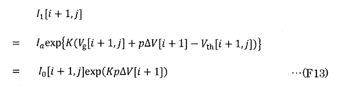
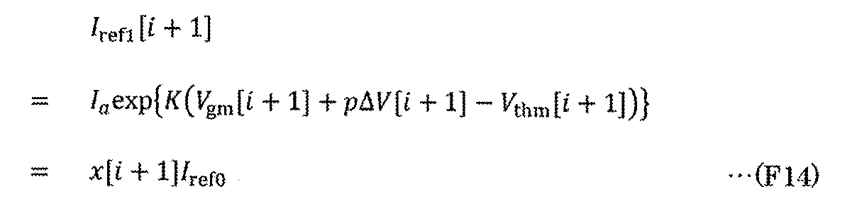


本実施の形態では、上記実施の形態で説明した演算回路の構成例、及び当該演算回路に適用可能なトランジスタの構成例について説明する。
図19に示す半導体装置は、トランジスタ300と、トランジスタ500と、容量素子600と、を有している。図21Aはトランジスタ500のチャネル長方向の断面図であり、図21Bはトランジスタ500のチャネル幅方向の断面図であり、図21Cはトランジスタ300のチャネル幅方向の断面図である。
本実施の形態では、上記の実施の形態で説明したOSトランジスタに用いることができる金属酸化物であるCAC−OS(Cloud−Aligned Composite Oxide Semiconductor)、及びCAAC−OS(c−axis Aligned Crystalline Oxide Semiconductor)の構成について説明する。
CAC−OS又はCAC−metal oxideとは、材料の一部では導電性の機能と、材料の一部では絶縁性の機能とを有し、材料の全体では半導体としての機能を有する。なお、CAC−OS又はCAC−metal oxideを、トランジスタの活性層に用いる場合、導電性の機能は、キャリアとなる電子(又はホール)を流す機能であり、絶縁性の機能は、キャリアとなる電子を流さない機能である。導電性の機能と、絶縁性の機能とを、それぞれ相補的に作用させることで、スイッチングさせる機能(On/Offさせる機能)をCAC−OS又はCAC−metal oxideに付与することができる。CAC−OS又はCAC−metal oxideにおいて、それぞれの機能を分離させることで、双方の機能を最大限に高めることができる。
酸化物半導体は、単結晶酸化物半導体と、それ以外の非単結晶酸化物半導体と、に分けられる。非単結晶酸化物半導体としては、例えば、CAAC−OS、多結晶酸化物半導体、nc−OS(nanocrystalline oxide semiconductor)、擬似非晶質酸化物半導体(a−like OS:amorphous−like oxide semiconductor)及び非晶質酸化物半導体などがある。
続いて、上記酸化物半導体をトランジスタに用いる場合について説明する。
ここで、酸化物半導体中における各不純物の影響について説明する。
図29Aに示す乗算回路AMEは、実際に試作した演算回路の一部であって、実施の形態2で説明した演算回路MAC1のメモリセルAMに相当する。そのため、乗算回路AMEに含まれているトランジスタM1、容量CPのそれぞれは、図9に示すメモリセルAMに含まれているトランジスタM1、容量C1に相当する。特に、乗算回路AMEに含まれているトランジスタM2−1、トランジスタM2−2は、図9に示すメモリセルAMに含まれているトランジスタM2に相当している。つまり、トランジスタM2−1とトランジスタM2−2が直列に電気的に接続され、互いのゲートが電気的に接続されている。なお、本実施例では、トランジスタM2−1、トランジスタM2−2をまとめてトランジスタM2と呼称する。また、図29Aに示す配線VYは、図9の配線BLに相当し、図29Aに示す配線BWは、図9の配線WDに相当し、図29Aに示す配線VXは、図9の配線CLに相当し、図29Aに示す配線WWは、図9の配線WLに相当する。




Claims (7)
- 第1電子機器を有し、
前記第1電子機器は、入出力インターフェースと、制御部と、第1変換部と、を有し、
前記入出力インターフェースは、前記制御部に電気的に接続され、
前記第1変換部は、前記制御部に電気的に接続され、
前記入出力インターフェースは、ユーザが操作することによって生成された入力データを前記制御部に送信する機能を有し、
前記制御部は、前記入力データを前記第1変換部に送信する機能を有し、
前記第1変換部は、ニューラルネットワークが構成された回路を有し、
前記第1変換部は、前記ニューラルネットワークによって前記入力データを第1ネットリストに変換する機能を有し、
前記入力データは、回路構成が描かれた回路図、又は前記回路構成が示された文書ファイルである、
AIシステム。 - 請求項1において、
前記第1電子機器は、第1データベースと、第2データベースと、を有し、
前記第1データベースは、前記制御部に電気的に接続され、
前記第2データベースは、前記制御部に電気的に接続され、
前記第1データベースには、第2ネットリストが保存されており、
前記第2データベースには、前記第2ネットリストに紐付けされた文献データが保存されており、
前記制御部は、
前記第1データベースを対象に、前記第1ネットリストの回路構成の検索を行う機能と、
前記第1ネットリストの回路構成の検索において、前記第2ネットリストが見つかった場合に、前記文献データを前記第2データベースから読み出して、前記入出力インターフェースに出力する機能と、を有する、
AIシステム。 - 請求項1において、
第2電子機器を有し、
前記第1電子機器は、外部インターフェースを有し、
前記第2電子機器は、第3データベースと、第4データベースと、を有し、
前記第3データベースは、前記外部インターフェースに電気的に接続され、
前記第4データベースは、前記外部インターフェースに電気的に接続され、
前記第3データベースには、第2ネットリストが保存されており、
前記第4データベースには、前記第2ネットリストに紐付けされた文献データが保存されており、
前記制御部は、前記外部インターフェースを介して、前記第2電子機器と通信を行って、
前記第3データベースを対象に、前記第1ネットリストの回路構成の検索を行う機能と、
前記第1ネットリストの回路構成の検索において、前記第3データベースから前記第2ネットリストが見つかった場合に、前記文献データを前記第4データベースから読み出して、前記入出力インターフェースに出力する機能と、を有する、
AIシステム。 - 第1電子機器と、第2電子機器と、を有し、
前記第1電子機器は、入出力インターフェースと、制御部と、外部インターフェースと、を有し、
前記第2電子機器は、第2変換部を有し、
前記入出力インターフェースは、前記制御部に電気的に接続され、
前記外部インターフェースは、前記制御部と、前記第2電子機器の前記第2変換部に電気的に接続され、
前記入出力インターフェースは、ユーザが操作することによって生成された入力データを前記制御部に送信する機能を有し、
前記制御部は、前記入力データを、前記外部インターフェースを介して、前記第2電子機器の前記第2変換部に送信する機能を有し、
前記第2変換部は、ニューラルネットワークが構成された回路を有し、
前記第2変換部は、前記ニューラルネットワークによって前記入力データを第1ネットリストに変換する機能を有し、
前記制御部は、前記外部インターフェースを介して、前記第2電子機器から前記第1ネットリストを取得する機能を有し、
前記入力データは、回路構成が描かれた回路図、又は前記回路構成が示された文書ファイルである、
AIシステム。 - 請求項4において、
前記第2電子機器は、第3データベースと、第4データベースと、を有し、
前記第3データベースは、前記外部インターフェースに電気的に接続され、
前記第4データベースは、前記外部インターフェースに電気的に接続され、
前記第3データベースには、第2ネットリストが保存されており、
前記第4データベースには、前記第2ネットリストに紐付けされた文献データが保存されており、
前記制御部は、前記外部インターフェースを介して、前記第2電子機器と通信を行って、
前記第3データベースを対象に、前記第1ネットリストの回路構成の検索を行う機能と、
前記第1ネットリストの回路構成の検索において、前記第3データベースから前記第2ネットリストが見つかった場合に、前記文献データを前記第4データベースから読み出して、前記入出力インターフェースに出力する機能と、を有する、
AIシステム。 - 入出力インターフェースと、制御部と、第1変換部と、を有し、
前記第1変換部は、ニューラルネットワークが構成された回路を有し、
前記入出力インターフェースは、前記制御部に電気的に接続され、
前記第1変換部は、前記制御部に電気的に接続されている、AIシステムの動作方法であって、
第1乃至第3ステップを有し、
前記第1ステップは、ユーザによって作成された入力データが、前記制御部に入力されるステップを有し、
前記第2ステップは、前記第1変換部の前記ニューラルネットワークによって、前記入力データを第1ネットリストに変換するステップを有し、
前記第3ステップは、前記制御部を介して、前記入出力インターフェースに出力するステップを有する、
AIシステムの動作方法。 - 請求項6において、第4乃至第6ステップを有し、
前記AIシステムは、第1データベースと、第2データベースと、を有し、
前記第1データベースは、前記制御部に電気的に接続され、
前記第2データベースは、前記制御部に電気的に接続され、
前記第1データベースには、第2ネットリストが保存されており、
前記第2データベースには、前記第2ネットリストに紐付けされた文献データが保存されており、
前記第4ステップは、前記第1データベースを対象に、前記第1ネットリストの回路構成の検索を行うステップを有し、
前記第5ステップは、前記第4ステップで前記第1データベースから前記第2ネットリストが見つかった場合に、前記文献データを前記第2データベースから読み出して、前記入出力インターフェースに出力するステップを有し、
前記第6ステップは、前記第4ステップで前記第1データベースから前記第2ネットリストが見つからなかった場合に、前記制御部が、前記第1ネットリストが前記第1データベースから見つからなかったという情報を前記入出力インターフェースに出力するステップを有する、
AIシステムの動作方法。
Priority Applications (10)
| Application Number | Priority Date | Filing Date | Title |
|---|---|---|---|
| KR1020217031325A KR20210135541A (ko) | 2019-03-08 | 2020-02-24 | Ai 시스템 및 ai 시스템의 동작 방법 |
| CN202080018555.2A CN113614727A (zh) | 2019-03-08 | 2020-02-24 | Ai系统及ai系统的工作方法 |
| JP2021504594A JP7462609B2 (ja) | 2019-03-08 | 2020-02-24 | Aiシステム、及びaiシステムの動作方法 |
| DE112020001142.9T DE112020001142T5 (de) | 2019-03-08 | 2020-02-24 | KI-System und Betriebsverfahren von KI-System |
| US17/436,467 US12456041B2 (en) | 2019-03-08 | 2020-02-24 | AI system and operation method of AI system |
| JP2024050193A JP7675887B2 (ja) | 2019-03-08 | 2024-03-26 | Aiシステム |
| JP2025073992A JP2025118717A (ja) | 2019-03-08 | 2025-04-28 | 検索システム |
| JP2025199045A JP7804827B1 (ja) | 2019-03-08 | 2025-11-19 | 演算回路 |
| JP2026002459A JP2026063036A (ja) | 2019-03-08 | 2026-01-09 | 演算回路 |
| JP2026003144A JP2026063062A (ja) | 2019-03-08 | 2026-01-12 | 演算回路 |
Applications Claiming Priority (6)
| Application Number | Priority Date | Filing Date | Title |
|---|---|---|---|
| JP2019-042594 | 2019-03-08 | ||
| JP2019042594 | 2019-03-08 | ||
| JP2019088049 | 2019-05-08 | ||
| JP2019-088049 | 2019-05-08 | ||
| JP2019-194669 | 2019-10-25 | ||
| JP2019194669 | 2019-10-25 |
Publications (1)
| Publication Number | Publication Date |
|---|---|
| WO2020183263A1 true WO2020183263A1 (ja) | 2020-09-17 |
Family
ID=72425955
Family Applications (1)
| Application Number | Title | Priority Date | Filing Date |
|---|---|---|---|
| PCT/IB2020/051516 Ceased WO2020183263A1 (ja) | 2019-03-08 | 2020-02-24 | Aiシステム、及びaiシステムの動作方法 |
Country Status (6)
| Country | Link |
|---|---|
| US (1) | US12456041B2 (ja) |
| JP (6) | JP7462609B2 (ja) |
| KR (1) | KR20210135541A (ja) |
| CN (1) | CN113614727A (ja) |
| DE (1) | DE112020001142T5 (ja) |
| WO (1) | WO2020183263A1 (ja) |
Cited By (1)
| Publication number | Priority date | Publication date | Assignee | Title |
|---|---|---|---|---|
| US12475361B2 (en) | 2019-05-17 | 2025-11-18 | Semiconductor Energy Laboratory Co., Ltd. | Semiconductor device and electronic device |
Families Citing this family (5)
| Publication number | Priority date | Publication date | Assignee | Title |
|---|---|---|---|---|
| US12033694B2 (en) | 2020-07-17 | 2024-07-09 | Semiconductor Energy Laboratory Co., Ltd. | Semiconductor device and electronic device |
| US12183287B2 (en) * | 2021-05-27 | 2024-12-31 | Semiconductor Energy Laboratory Co., Ltd. | Semiconductor device, display apparatus, and electronic device |
| CN114357857B (zh) * | 2021-12-03 | 2025-06-06 | 深圳先进技术研究院 | 机器人辅助数字化可控合成纳米晶体形貌的方法 |
| CN114818024B (zh) * | 2022-06-28 | 2022-10-14 | 电子科技大学 | 一种磁谐振三相无线充电线圈自动化仿真方法 |
| US12443611B2 (en) * | 2022-08-15 | 2025-10-14 | CELUS GmbH | Systems and methods for automated electronics design and graphical user interface |
Citations (2)
| Publication number | Priority date | Publication date | Assignee | Title |
|---|---|---|---|---|
| JP2015176193A (ja) * | 2014-03-13 | 2015-10-05 | Necプラットフォームズ株式会社 | 設計支援装置および設計支援方法 |
| JP2018005436A (ja) * | 2016-06-30 | 2018-01-11 | 株式会社日立製作所 | 回路設計装置及びそれを用いた回路設計方法 |
Family Cites Families (22)
| Publication number | Priority date | Publication date | Assignee | Title |
|---|---|---|---|---|
| JPH07200643A (ja) * | 1993-12-28 | 1995-08-04 | Fujitsu Ltd | 半導体集積回路のレイアウトデータ抽出方法及び抽出装置 |
| US20070256037A1 (en) * | 2006-04-26 | 2007-11-01 | Zavadsky Vyacheslav L | Net-list organization tools |
| US7937678B2 (en) * | 2008-06-11 | 2011-05-03 | Infineon Technologies Ag | System and method for integrated circuit planar netlist interpretation |
| EP2808828B1 (en) | 2013-05-31 | 2020-08-05 | Omron Corporation | Image matching method, image matching device, model template generation method, model template generation device, and program |
| JP6589313B2 (ja) | 2014-04-11 | 2019-10-16 | 株式会社リコー | 視差値導出装置、機器制御システム、移動体、ロボット、視差値導出方法、およびプログラム |
| US10102320B2 (en) * | 2015-02-26 | 2018-10-16 | Autodesk, Inc. | Predictive multi-user client-server electronic circuit design system utilizing machine learning techniques |
| WO2017017808A1 (ja) | 2015-07-29 | 2017-02-02 | 株式会社日立製作所 | 画像処理システム、画像処理方法及び記憶媒体 |
| FR3050050B1 (fr) * | 2016-04-11 | 2021-10-15 | Univ De Lille 1 | Neurone artificiel |
| US10109633B2 (en) | 2016-04-27 | 2018-10-23 | Semiconductor Energy Laboratory Co., Ltd. | Semiconductor device, electronic device, and authentication system |
| WO2018002774A1 (en) | 2016-06-29 | 2018-01-04 | Semiconductor Energy Laboratory Co., Ltd. | Electronic device, operation method of the electronic device, and moving vehicle |
| JP7012298B2 (ja) | 2016-09-21 | 2022-01-28 | ジャパンモード株式会社 | 文献データ解析プログラム及びシステム |
| WO2018069785A1 (en) * | 2016-10-12 | 2018-04-19 | Semiconductor Energy Laboratory Co., Ltd. | Semiconductor device and system using the same |
| WO2018221625A1 (ja) | 2017-05-30 | 2018-12-06 | 国立大学法人東北大学 | 皮膚組織の病理画像を用いた診断支援のためのシステム及び方法 |
| WO2018224910A1 (ja) * | 2017-06-08 | 2018-12-13 | 株式会社半導体エネルギー研究所 | 撮像装置および電子機器 |
| JP7146751B2 (ja) | 2017-06-22 | 2022-10-04 | 株式会社半導体エネルギー研究所 | レイアウト設計システム及びレイアウト設計方法 |
| WO2019021095A1 (ja) | 2017-07-26 | 2019-01-31 | 株式会社半導体エネルギー研究所 | 二次電池の充電制御システム及び二次電池の異常検出方法 |
| JP6901939B2 (ja) * | 2017-08-11 | 2021-07-14 | 株式会社半導体エネルギー研究所 | 半導体装置、及び電子機器 |
| US11010516B2 (en) * | 2018-11-09 | 2021-05-18 | Nvidia Corp. | Deep learning based identification of difficult to test nodes |
| US20220215146A1 (en) * | 2020-08-18 | 2022-07-07 | Anaglobe Technology, Inc. | Method for recognizing analog circuit structure |
| JP7667009B2 (ja) * | 2021-07-27 | 2025-04-22 | 東芝テック株式会社 | 販売データ処理システムおよびプログラム |
| CN115017850B (zh) * | 2022-06-20 | 2024-11-15 | 东南大学 | 一种数字集成电路优化方法 |
| US12475291B2 (en) * | 2022-09-09 | 2025-11-18 | Anaglobe Technology, Inc. | Method for generating analog schematic diagram based on building block classification and reinforcement learning |
-
2020
- 2020-02-24 JP JP2021504594A patent/JP7462609B2/ja active Active
- 2020-02-24 WO PCT/IB2020/051516 patent/WO2020183263A1/ja not_active Ceased
- 2020-02-24 DE DE112020001142.9T patent/DE112020001142T5/de active Pending
- 2020-02-24 CN CN202080018555.2A patent/CN113614727A/zh active Pending
- 2020-02-24 US US17/436,467 patent/US12456041B2/en active Active
- 2020-02-24 KR KR1020217031325A patent/KR20210135541A/ko active Pending
-
2024
- 2024-03-26 JP JP2024050193A patent/JP7675887B2/ja active Active
-
2025
- 2025-04-28 JP JP2025073992A patent/JP2025118717A/ja active Pending
- 2025-11-19 JP JP2025199045A patent/JP7804827B1/ja active Active
-
2026
- 2026-01-09 JP JP2026002459A patent/JP2026063036A/ja active Pending
- 2026-01-12 JP JP2026003144A patent/JP2026063062A/ja active Pending
Patent Citations (2)
| Publication number | Priority date | Publication date | Assignee | Title |
|---|---|---|---|---|
| JP2015176193A (ja) * | 2014-03-13 | 2015-10-05 | Necプラットフォームズ株式会社 | 設計支援装置および設計支援方法 |
| JP2018005436A (ja) * | 2016-06-30 | 2018-01-11 | 株式会社日立製作所 | 回路設計装置及びそれを用いた回路設計方法 |
Cited By (1)
| Publication number | Priority date | Publication date | Assignee | Title |
|---|---|---|---|---|
| US12475361B2 (en) | 2019-05-17 | 2025-11-18 | Semiconductor Energy Laboratory Co., Ltd. | Semiconductor device and electronic device |
Also Published As
| Publication number | Publication date |
|---|---|
| US20220180159A1 (en) | 2022-06-09 |
| JPWO2020183263A1 (ja) | 2020-09-17 |
| JP2025118717A (ja) | 2025-08-13 |
| JP2026063062A (ja) | 2026-04-10 |
| JP7804827B1 (ja) | 2026-01-22 |
| DE112020001142T5 (de) | 2021-11-18 |
| US12456041B2 (en) | 2025-10-28 |
| KR20210135541A (ko) | 2021-11-15 |
| JP2026041783A (ja) | 2026-03-10 |
| JP2026063036A (ja) | 2026-04-10 |
| CN113614727A (zh) | 2021-11-05 |
| JP7462609B2 (ja) | 2024-04-05 |
| JP7675887B2 (ja) | 2025-05-13 |
| JP2024079789A (ja) | 2024-06-11 |
Similar Documents
| Publication | Publication Date | Title |
|---|---|---|
| JP7675887B2 (ja) | Aiシステム | |
| JP7234110B2 (ja) | メモリセル及び半導体装置 | |
| JP7337782B2 (ja) | 半導体装置 | |
| JP2019047006A (ja) | 半導体装置、電子機器 | |
| JP2024061728A (ja) | 半導体装置 | |
| JP7689126B2 (ja) | 半導体装置、及び電子機器 | |
| US20200125935A1 (en) | Semiconductor device having neural network | |
| JP7480133B2 (ja) | 半導体装置、及び電子機器 | |
| US20250174259A1 (en) | Semiconductor device and electronic device | |
| JP2025060890A (ja) | 半導体装置 | |
| JP7395566B2 (ja) | 検査方法 | |
| Park et al. | CMOS-compatible low-power gated diode synaptic device for hardware-based neural network | |
| JP2025159013A (ja) | 半導体装置 | |
| US20240143441A1 (en) | Operation method of semiconductor device | |
| JP2018106608A (ja) | 半導体装置 | |
| Oberoi | Engineering hole injection and transport in low-dimensional material transistors | |
| US20250362876A1 (en) | Semiconductor Device And Electronic Device | |
| US20250280531A1 (en) | Semiconductor device and electronic device | |
| JP2019021219A (ja) | 集積回路、モジュール、コンピュータ、電子機器及びシステム | |
| WO2025181636A1 (ja) | 半導体装置、演算装置及び電子機器 | |
| WO2026013524A1 (ja) | 半導体装置 | |
| JP2019008655A (ja) | 集積回路、コンピュータ及び電子機器 |
Legal Events
| Date | Code | Title | Description |
|---|---|---|---|
| 121 | Ep: the epo has been informed by wipo that ep was designated in this application |
Ref document number: 20770749 Country of ref document: EP Kind code of ref document: A1 |
|
| ENP | Entry into the national phase |
Ref document number: 2021504594 Country of ref document: JP Kind code of ref document: A |
|
| ENP | Entry into the national phase |
Ref document number: 20217031325 Country of ref document: KR Kind code of ref document: A |
|
| 122 | Ep: pct application non-entry in european phase |
Ref document number: 20770749 Country of ref document: EP Kind code of ref document: A1 |
|
| WWG | Wipo information: grant in national office |
Ref document number: 17436467 Country of ref document: US |