WO2020179452A1 - 容量素子、半導体素子基板及び電子機器 - Google Patents
容量素子、半導体素子基板及び電子機器 Download PDFInfo
- Publication number
- WO2020179452A1 WO2020179452A1 PCT/JP2020/006552 JP2020006552W WO2020179452A1 WO 2020179452 A1 WO2020179452 A1 WO 2020179452A1 JP 2020006552 W JP2020006552 W JP 2020006552W WO 2020179452 A1 WO2020179452 A1 WO 2020179452A1
- Authority
- WO
- WIPO (PCT)
- Prior art keywords
- conductive film
- substrate
- capacitive element
- layer
- electrode
- Prior art date
- Legal status (The legal status is an assumption and is not a legal conclusion. Google has not performed a legal analysis and makes no representation as to the accuracy of the status listed.)
- Ceased
Links
Images




Classifications
-
- H—ELECTRICITY
- H10—SEMICONDUCTOR DEVICES; ELECTRIC SOLID-STATE DEVICES NOT OTHERWISE PROVIDED FOR
- H10D—INORGANIC ELECTRIC SEMICONDUCTOR DEVICES
- H10D84/00—Integrated devices formed in or on semiconductor substrates that comprise only semiconducting layers, e.g. on Si wafers or on GaAs-on-Si wafers
-
- H—ELECTRICITY
- H10—SEMICONDUCTOR DEVICES; ELECTRIC SOLID-STATE DEVICES NOT OTHERWISE PROVIDED FOR
- H10D—INORGANIC ELECTRIC SEMICONDUCTOR DEVICES
- H10D84/00—Integrated devices formed in or on semiconductor substrates that comprise only semiconducting layers, e.g. on Si wafers or on GaAs-on-Si wafers
- H10D84/01—Manufacture or treatment
- H10D84/02—Manufacture or treatment characterised by using material-based technologies
- H10D84/03—Manufacture or treatment characterised by using material-based technologies using Group IV technology, e.g. silicon technology or silicon-carbide [SiC] technology
- H10D84/038—Manufacture or treatment characterised by using material-based technologies using Group IV technology, e.g. silicon technology or silicon-carbide [SiC] technology using silicon technology, e.g. SiGe
-
- H—ELECTRICITY
- H10—SEMICONDUCTOR DEVICES; ELECTRIC SOLID-STATE DEVICES NOT OTHERWISE PROVIDED FOR
- H10P—GENERIC PROCESSES OR APPARATUS FOR THE MANUFACTURE OR TREATMENT OF DEVICES COVERED BY CLASS H10
- H10P14/00—Formation of materials, e.g. in the shape of layers or pillars
- H10P14/40—Formation of materials, e.g. in the shape of layers or pillars of conductive or resistive materials
-
- H—ELECTRICITY
- H10—SEMICONDUCTOR DEVICES; ELECTRIC SOLID-STATE DEVICES NOT OTHERWISE PROVIDED FOR
- H10W—GENERIC PACKAGES, INTERCONNECTIONS, CONNECTORS OR OTHER CONSTRUCTIONAL DETAILS OF DEVICES COVERED BY CLASS H10
- H10W20/00—Interconnections in chips, wafers or substrates
- H10W20/01—Manufacture or treatment
-
- H—ELECTRICITY
- H10—SEMICONDUCTOR DEVICES; ELECTRIC SOLID-STATE DEVICES NOT OTHERWISE PROVIDED FOR
- H10W—GENERIC PACKAGES, INTERCONNECTIONS, CONNECTORS OR OTHER CONSTRUCTIONAL DETAILS OF DEVICES COVERED BY CLASS H10
- H10W20/00—Interconnections in chips, wafers or substrates
- H10W20/40—Interconnections external to wafers or substrates, e.g. back-end-of-line [BEOL] metallisations or vias connecting to gate electrodes
-
- H—ELECTRICITY
- H10—SEMICONDUCTOR DEVICES; ELECTRIC SOLID-STATE DEVICES NOT OTHERWISE PROVIDED FOR
- H10W—GENERIC PACKAGES, INTERCONNECTIONS, CONNECTORS OR OTHER CONSTRUCTIONAL DETAILS OF DEVICES COVERED BY CLASS H10
- H10W70/00—Package substrates; Interposers; Redistribution layers [RDL]
- H10W70/60—Insulating or insulated package substrates; Interposers; Redistribution layers
-
- H—ELECTRICITY
- H10—SEMICONDUCTOR DEVICES; ELECTRIC SOLID-STATE DEVICES NOT OTHERWISE PROVIDED FOR
- H10W—GENERIC PACKAGES, INTERCONNECTIONS, CONNECTORS OR OTHER CONSTRUCTIONAL DETAILS OF DEVICES COVERED BY CLASS H10
- H10W90/00—Package configurations
Definitions
- the present disclosure relates to capacitive elements, semiconductor element substrates and electronic devices.
- a large-capacity capacitive element is required depending on the circuit configuration.
- a charge pump circuit in a logic chip of a tested and compensated bare die (TD: Tested Die) product requires a large-capacity element in order to ensure power supply capacity and stable operation.
- the capacitance (electrostatic capacitance) of the capacitive element is proportional to the area of the parallel flat plate conductor, assuming parallel flat plate conductors that are opposed to each other via a dielectric as the capacitive element. Therefore, even in an actual capacitive element, the installation area of the capacitive element is also increased in order to increase the capacitance.
- the present disclosure has been made in view of such a situation, and when provided on a semiconductor substrate, a capacitance element capable of ensuring capacitance while reducing the installation area and a semiconductor element substrate having a small installation area. And the purpose is to provide electronic devices.
- the capacitive element of the present disclosure is arranged so as to face each other on the inner peripheral surface of a through hole formed so as to penetrate from the first surface of the insulator substrate to the opposite second surface.
- a plurality of conductive layers and a dielectric layer formed between a pair of opposing conductive layers at least one of the plurality of conductive layers constituting a capacitive element. As one of them, it is possible to connect to the circuit wiring formed on the second surface side.
- FIG. 1 is a partial cross-sectional view when the capacitive element of the first embodiment is applied to a semiconductor element substrate having a laminated structure.
- the semiconductor element substrate 10 includes a first silicon (Si) substrate 11, a solder resist layer 12 laminated on the first surface (lower surface in the figure) P1 side of the first silicon substrate 11, and a first silicon substrate.
- the capacitive element 14 has a cylindrical shape with a bottom in the first through hole 13-1 when the upper electrode 19 side is regarded as the bottom side, and is on the first surface P1 of the first silicon substrate 11.
- the dielectric layer 32 functioning as a dielectric (insulator) that constitutes the capacitive element 14, and the first conductive film layer 33 via the dielectric layer 32.
- has a bottomed cylindrical shape inside the first through hole 13-1, and wiring to each part and wiring to the silicon through electrode 15 are performed on the first surface P1 of the first silicon substrate 11. It includes two conductive layers 31.
- the through silicon via 15 has a bottomed cylindrical shape in the first through hole 13-2 like the capacitance element 14, and wiring to each portion is made on the first surface P1 of the first silicon substrate 11.
- the first conductive film layer 33 is provided.
- the first conductive film layer 33 constituting the capacitive element 14 is electrically connected to the upper electrode 19 on the first surface P1 side of the first silicon substrate 11, and constitutes the through silicon via 15.
- the first conductive film layer 33 connected to the second conductive film layer 31 is electrically connected to the lower electrode 21 on the first surface P1 side of the first silicon substrate 11.
- the capacitive element 14 has a structure in which the dielectric layer 32 is sandwiched between the first conductive film layer 33 and the second conductive film layer 31. Therefore, the capacitive element 14 functions as a capacitor connected between the upper electrode 19 and the lower electrode 21, and by extension, the first wiring 20 and the second wiring 22.
- FIG. 2 is an explanatory diagram (Part 1) of the manufacturing process of the capacitive element of the first embodiment.
- FIG. 3 is an explanatory view (No. 2) of the manufacturing process of the capacitive element of the first embodiment.
- a first through hole 13-1 and a second through hole 13-1 as TSV are previously formed in the first silicon substrate 11 by a dry etching method or the like. I shall. Further, it is assumed that the first insulator layer 16 on which the upper electrode 19 and the lower electrode 21 are formed is laminated on the second surface P2 of the first silicon substrate 11.
- the first conductive film layer 33 and the dielectric layer 32 are formed.
- a titanium layer is formed on the first silicon substrate 11 by a sputtering method
- a copper layer is formed on the titanium layer by a CVD (Chemical Vapor Deposition) method
- a first conductive film layer is formed by a wet RDL (Redistribution Layer). 33 is formed.
- a SiO layer is formed as the dielectric layer 32 by the CVD method, and the excess SiO layer is removed by the electron beam (EB) removal method to obtain the dielectric layer 32 having a desired shape.
- EB electron beam
- the second conductive film layer 31 is formed. Specifically, for example, similar to the formation of the first conductive film layer 33, a titanium layer is formed on the first silicon substrate 11 by a sputtering method, a copper layer is formed on the titanium layer by a CVD method, and a second layer is formed by wet RDL. The conductive film layer 31 is formed.
- a photomask MSK is arranged so as to protect the second conductive film layer 31 forming the capacitive element 14.
- the extra second conductive film layer 31 is removed.
- the second conductive film layer 31 other than the portion where the photomask MSK is arranged is removed by an electron beam removing method or the like.
- a SiO layer as an insulator layer 41 for electrically insulating and physically protecting the second conductive film layer 31 is formed by a CVD method or the like.
- the photomask MSK is arranged again so as to protect the insulator layer 41 laminated on the second conductive film layer 31 forming the capacitive element 14.
- the extra insulator layer 41 is removed. Specifically, the insulator layer 41 other than the portion where the photomask MSK is arranged is removed by an electron beam removing method or the like. As a result, when the photomask MSK is arranged as shown in FIG. 3D, as shown in FIG. 3E, in the insulator layer 41, except the portion laminated on the second conductive film layer 31. The insulating layer 41 is removed to form the capacitive element 14 shown in FIG.
- the capacitive element 14 is arranged in the TSV formed on the insulating substrate (first silicon substrate), and the back surface side of the insulating substrate (first silicon substrate 11 of the first silicon substrate 11) which has not been used conventionally is arranged.
- the capacitive element 14 By using the area on the surface P1 side for the wiring of the capacitive element 14, a large-scale capacitive element can be mounted without pressing the existing design area, and a higher integration of the target circuit can be realized.
- FIG. 4 is an explanatory diagram of a semiconductor device according to a first modified example of the first embodiment.
- the semiconductor element substrate 10B of the present modified example is different from the semiconductor element substrate 10 of the first embodiment in that the second silicon conductive film layer 31 is not the silicon through electrode 15 but the first silicon substrate 11 via the conductive film layer 34. It is a point connected to a copper pillar 37 formed as an electrode terminal for connecting a flip tip on the P1 side of the first surface of the above. Accordingly, even when the semiconductor element substrate 10B is provided on an external substrate (not shown), an electronic device can be constructed without causing an unnecessary increase in mounting area.
- the pillar electrodes (copper pillars 37) are provided on the semiconductor element substrate 10B. However, one of the pair of electrodes forming the capacitive element 14 is formed by providing the bump electrodes. May be connected to the bump electrode.
- FIG. 5 is an explanatory diagram of a semiconductor device according to a second modification of the first embodiment.
- the semiconductor element substrate 10C of the present modification is different from the semiconductor element substrate 10 of the first embodiment in that a plurality of capacitance elements 14-1 to 14-5 similar to the capacitance element 14 are provided, and the capacitance elements 14-1 to 14-5 are commonly connected to the first conductive film layer 33 and are connected to the upper electrode 19, and the second conductive film layers 33 of the capacitors 14-1 to 14-5 are commonly connected to form a silicon through electrode. It is a point connected to the lower electrode 21 via 15.
- Capacitive capacitive elements can be constructed.
- the capacitance element 14 when the capacitance of each of the capacitance elements 14-1 to 14-5 is 16 pF as in the case of the concrete example of the first embodiment, the capacitance element 14 according to the second modification of FIG.
- FIG. 6 is an external view of the first silicon substrate in the semiconductor element substrate of the specific example of the first embodiment.
- the first silicon substrate 11 forming the semiconductor element substrate 10 has a sandy pattern area AR in the figure. No component placement area or wiring placement area is provided.
- a plurality of regions correspond to the region AR. It forms a capacitive element.
- the capacitance is formed by the conventional method with the same installation area, it is about 940 pF, which can be sufficiently replaced.
- the installation area of the semiconductor element substrate can be reduced by about 3%. Therefore, according to the first embodiment, it is possible to easily reduce the size of the semiconductor element substrate and thus the electronic device using the semiconductor element substrate.
- FIG. 7 is a partial cross-sectional view when the capacitive element of the second embodiment is applied to a semiconductor element substrate having a laminated structure.
- the semiconductor element substrate 10 of the first embodiment has the same structure as the second insulator layer 17 and above. Is omitted. Further, in FIG. 7, the same parts as those in FIG. 1 are designated by the same reference numerals.
- the semiconductor element substrate 100 includes a first silicon substrate 11, a solder resist layer 12 laminated on the first surface P1 side of the first silicon substrate 11, and a first surface P1 to a second surface of the silicon substrate 11.
- the silicon through electrode 15 formed in the second through hole 13-2 formed as a TSV penetrating the substrate, the first insulator layer 16 laminated on the second surface P2 of the silicon substrate 11, and the first insulation
- the second insulator layer 17 laminated on the body layer 16, the second silicon substrate 18 on which the solid-state image sensor is formed, and the first insulator layer 16 are formed and connected to one electrode of the capacitor element 14.
- the capacitive element 14A has a bottomed cylindrical shape in the first through hole 13-1 when the upper electrode 19 side is regarded as the bottom side, and is on the first surface P1 of the first silicon substrate 11.
- the first conductive film layer 33-1 electrically connected to the conductive film layer 33 constituting the first electrode (electrode A) to which wiring is made to each part, and the dielectric material constituting the capacitive element 14 (
- the first dielectric layer 32-1 that functions as an insulator) and the first conductive layer 33-1 are opposed to each other via the first dielectric layer 32-1 and are present in the first through hole 13-1.
- the conductive film layer 34 which has a bottom cylindrical shape and constitutes a second electrode (electrode B) in which wiring to each part and wiring to the silicon penetrating electrode 15 are made on the first surface P1 of the first silicon substrate 11. It includes a second conductive film layer 34-1 that is electrically connected, and a second dielectric layer 32-2 that functions as a dielectric (insulator) constituting the capacitive element 14. Further, the capacitive element 14A faces the second conductive film layer 33-2 via the second dielectric layer 32-2, and has a bottomed cylindrical shape in the first through hole 13-1.
- a third conductive film layer 34-2 that is electrically connected to a conductive film layer 33 that constitutes a first electrode (electrode A) in which wiring is made to each portion on the first surface P1 of the silicon substrate 11.
- a third dielectric layer 32-3 that functions as a dielectric (insulator) that constitutes the capacitive element 14.
- the capacitive element 14A faces the third conductive film layer 33-2 via the third dielectric layer 32-3, and has a bottomed cylindrical shape in the first through hole 13-1.
- the conductive film layer 34-2 is provided.
- the silicon through electrode 15 has a bottomed cylindrical shape in the first through hole 13-2, as in the first embodiment, and wiring to each part on the first surface P1 of the first silicon substrate 11 is provided.
- the conductive film layer 34 is provided.
- the first conductive film layer 33-1 constituting the capacitive element 14A, and by extension, the third conductive film layer 33-2 and the conductive film layer 33 are located above the first surface P1 side of the first silicon substrate 11. It is electrically connected to the electrode 19.
- the second conductive film layer 34-1 which constitutes the silicon through electrode 15 and is connected to the conductive film layer 34, and thus the fourth conductive film layer 34-2 is the first surface P1 of the first silicon substrate 11. On the side, it is electrically connected to the lower electrode 21.
- the capacitive element 14A functions as three capacitors connected in parallel between the upper electrode 19 and the lower electrode 21, and by extension, the first wiring 20 and the second wiring.
- the capacitance when the capacitance is formed by the conventional method in the same installation area, it is about 940 pF. Therefore, in order to secure the capacitance similar to the conventional one, the semiconductor element substrate is installed. It is possible to reduce the area by about 30%. Therefore, according to the second embodiment, it is possible to form a capacitive element having a larger capacitance with the same installation area as compared with the first embodiment, and the semiconductor element substrate and thus the semiconductor element substrate is used. It is possible to easily further reduce the size of the electronic device.
- the capacitors are made to function as three capacitors connected in parallel, but if the third dielectric layer 32-3 and the fourth conductive film layer 34-2 are not provided, two capacitors are provided. It is possible to function as capacitors connected in parallel, and it is also possible to function as four capacitors connected in parallel as long as the manufacturing process permits.
- FIG. 8 is a partial cross-sectional view when the capacitive element of the third embodiment is applied to a semiconductor element substrate having a laminated structure.
- the semiconductor element substrate 10E of the third embodiment has the same structure as the semiconductor element substrate 10 of the first embodiment from the second insulator layer 17 onward, and thus is illustrated. For the sake of simplicity, these illustrations are omitted. Further, in FIG. 8, the same parts as those in FIG. 1 are designated by the same reference numerals.
- the semiconductor element substrate 10E of the third embodiment is different from the semiconductor element substrate 10 of the first embodiment between the first silicon substrate 11 and the first insulator layer 16 and the capacitive element 14B or the silicon through electrode 15B.
- the third insulating layer 51 is provided in the above.
- the inner peripheral surface of the first through hole 13-1 can be smoothed as compared with the case where the first through hole 13-1 is simply formed by the dry etching method or the like. It is possible to suppress the stability of processing in the formation of the capacitive element of the above, and by extension, the fluctuation of the capacitance of the formed capacitive element.
- FIG. 9 is an explanatory diagram (1) of the manufacturing process of the capacitive element of the third embodiment.
- FIG. 10 is an explanatory view (No. 2) of the manufacturing process of the capacitive element according to the third embodiment.
- a first through hole 13-1 and a second through hole 13-1 as TSV are previously formed in the first silicon substrate 11 by a dry etching method or the like. I shall.
- the first insulator layer 16 having the upper electrode 19 and the lower electrode 21 formed thereon, and the second insulator having the first wiring 20 and the second wiring 22 formed thereon are laminated.
- the third insulator layer 51 is formed.
- the SiO layer as the third insulator layer 51 is formed by the CVD method or the like.
- the first conductive film layer 33 is formed.
- a titanium layer is formed by a sputtering method
- a copper layer is formed on the titanium layer by a CVD method
- a first conductive film layer 33 is formed by wet RDL.
- a dielectric layer 32 is formed. Specifically, the SiO layer as the dielectric layer 32 is formed by the CVD method. Next, as shown in FIG. 10A, the excess SiO layer is removed to form the dielectric layer 32 having a desired shape. Specifically, the excess SiO layer is removed by an electron beam removing method of removing the dielectric layer 32 by irradiating it with an electron beam to obtain the dielectric layer 32 having a desired shape.
- the second conductive film layer 33 is formed. Specifically, for example, similar to the formation of the first conductive film layer 33, a titanium layer is formed on the first silicon substrate 11 by a sputtering method, a copper layer is formed on the titanium layer by a CVD method, and a second layer is formed by wet RDL. The conductive film layer 31 is formed.
- the solder resist layer 12 is formed by laminating it on the first surface (lower surface in the figure) P1 side of the first silicon substrate 11. Specifically, the solder resist layer 12 is formed by a printing method. As a result, a semiconductor element substrate having the capacitive element 14 of the third embodiment shown in FIG. 8 is obtained.
- FIG. 11 is an external view of a digital still camera as an electronic device to which the capacitive element and the semiconductor element substrate of each of the above embodiments are applied.
- a camera body (camera body) 50 of a lens interchangeable single-lens reflex type digital still camera as an electronic device includes a semiconductor element substrate (for example, a CMOS image sensor substrate) having the above-described capacitive element 14 as an imaging device.
- the semiconductor element substrate 10 is built in.
- the charge pump circuit in which the capacitative element constitutes the power supply circuit has been described as an example, but the same is applicable as long as the semiconductor element substrate includes a circuit that requires a large capacity capacitative element. is there.
- the case where the capacitive elements are connected in parallel has been described, but it is also possible to perform wiring so that at least a part of the capacitive elements are connected in series as necessary, such as for capacitance adjustment.
- the case where SiO2 is used as the material of the insulating layer has been described, but other insulating materials such as SiN can be used as the material of the insulating layer.
- the same conductive material as the silicon through electrode was used as one of the conductive layers of the capacitive element, but it is also possible to use a different conductive material.
- the capacitive element is arranged in the through hole (TSV) formed in the insulating substrate, and the back surface of the insulating substrate that has not been used conventionally is used.
- TSV through hole
- the semiconductor element substrate that uses the area on the side for wiring of the capacitive element, it is possible to mount a large-scale capacitive element without pressing the existing design area and achieve higher integration of the target circuit. it can. As a result, the electronic circuit using the target circuit can be easily downsized.
- this technology can also adopt the following configurations.
- Capacitive element Capacitive element.
- the conductive film layer is provided at least three or more, The capacitive element according to (1), wherein the two conductive layers and the conductive film layers arranged via the one conductive film layer are commonly connected to each other.
- the capacitive element according to (1) or (2) comprising an insulator layer formed between the through hole and the conductive film layer formed on the outermost peripheral side.
- An insulator substrate A plurality of conductive film layers arranged so as to face each other on the inner peripheral surface of the through hole formed so as to penetrate from the first surface to the second surface on the opposite side of the insulator substrate, and a pair of conductive layers facing each other.
- a capacitive element having a dielectric layer formed between the film layers is provided. At least one of the plurality of conductive film layers is connected to the circuit wiring formed on the second surface side as any one of the pair of electrodes constituting the capacitive element.
- Semiconductor device substrate is provided.
- the conductive film layer is provided at least three or more, The semiconductor device substrate according to (4), wherein the two conductive layers and the conductive film layers arranged via the one conductive film layer are commonly connected to each other.
- the semiconductor element substrate has a through electrode, a pillar electrode or a bump electrode provided on the insulator substrate, (4) or (5), wherein any one of the pair of electrodes constituting the capacitive element is connected to a through electrode, a pillar electrode, or a bump electrode provided on the insulator substrate.
- Semiconductor element substrate is provided at least three or more, The semiconductor device substrate according to (4), wherein the two conductive layers and the conductive film layers arranged via the one conductive film layer are commonly connected to each other.
- the semiconductor element substrate has a through electrode, a pillar electrode or a bump electrode provided on the insulator substrate, (4) or (5), wherein any one of the pair of electrodes constituting the capacitive element is connected to a through electrode, a pillar electrode, or
- the insulator substrate is provided with a plurality of the through holes, and the capacitance element is formed in each of the plurality of through holes, and one of the electrodes of one of the capacitance elements has the other capacitance.
- the semiconductor element substrate according to any one of (4) to (6), which is commonly connected to either of the other electrodes of the element.
- It has a second insulator substrate laminated on the insulator substrate, and an electrode of the capacitive element is connected to a circuit wiring formed on the second insulator substrate through the through hole.
- the semiconductor device substrate according to any one of (4) to (7).
- An insulator substrate A plurality of conductive layers arranged so as to face each other on the inner peripheral surface of the through hole formed so as to penetrate from the first surface to the second surface on the opposite side of the insulator substrate, and a pair of conductive layers facing each other.
- a dielectric layer formed between the film layers is provided, and at least one of the plurality of conductive film layers is formed on the second surface side as one of a pair of electrodes constituting a capacitive element.
- An electronic device having an electronic circuit having a capacitive element that can be connected to a circuit wiring.
- At least three or more conductive film layers are provided.
- An electronic device including an electronic circuit having a semiconductor element substrate connected to the circuit wiring formed on the second surface side as one side. (13) In the semiconductor element substrate, at least three or more conductive film layers are provided. The electronic device according to (12), wherein the conductive film layers arranged via the two dielectric layers and one conductive film layer are commonly connected to each other. (14)
- the semiconductor element substrate has a through electrode, a pillar electrode or a bump electrode provided on the insulator substrate, (12) or (13), wherein any one of the pair of electrodes constituting the capacitive element is connected to a through electrode, a pillar electrode, or a bump electrode provided on the insulator substrate. Electronic equipment.
- the insulator substrate is provided with a plurality of the through holes, and the capacitance element is formed in each of the plurality of through holes, and one of the electrodes of one of the capacitance elements has the other capacitance.
Landscapes
- Semiconductor Integrated Circuits (AREA)
- Internal Circuitry In Semiconductor Integrated Circuit Devices (AREA)
Abstract
本開示の容量素子(14)は、絶縁体基板(11)の第1面(P1)から反対側の第2面(P2)に貫通するように形成された貫通孔(13-1)の内周面において互いに対向するように配置された複数の導電膜層(31,33)と、対向する一対の導電膜層(31,33)間に形成された誘電体層(32)と、を備え、複数の導電膜層31,33)のうち、いずれか少なくとも一つが容量素子(14)を構成する一対の電極のうちいずれか一方として第2面(P2)側に形成された回路配線(20)に接続可能とされている。
Description
本開示は、容量素子、半導体素子基板及び電子機器に関する。
従来、回路構成によっては、大容量の容量素子が必要とされている。
例えば、テスト済み補償のベア・ダイ(TD:Tested Die)製品のロジックチップ内のチャージポンプ回路には、電源容量及び安定動作を確保するため、大規模容量素子が必要とされている。
例えば、テスト済み補償のベア・ダイ(TD:Tested Die)製品のロジックチップ内のチャージポンプ回路には、電源容量及び安定動作を確保するため、大規模容量素子が必要とされている。
ところで容量素子の容量(静電容量)は、容量素子として誘電体を介して対向配置された平行平板導体を想定した場合、平行平板導体の面積に比例している。
したがって、実際の容量素子においても、容量を大きくするためには、容量素子の設置面積も増大することとなっていた。
したがって、実際の容量素子においても、容量を大きくするためには、容量素子の設置面積も増大することとなっていた。
ところで、面積制約の大きい製品チップ内に大規模容量素子を搭載することは回路の高集積化に対する影響が大きく、次世代タイプのチップサイズシュリンクにおいて課題となることが容易に想定される。したがって、可能な限り容量素子の設置面積を縮小することが望まれている。
本開示は、このような状況に鑑みてなされたものであり、半導体基板上に設ける場合に、設置面積を低減しつつ、容量を確保することが可能な容量素子及び設置面積の少ない半導体素子基板及び電子機器を提供することを目的としている。
上記目的を達成するために、本開示の容量素子は、絶縁体基板の第1面から反対側の第2面に貫通するように形成された貫通孔の内周面において互いに対向するように配置された複数の導電膜層と、対向する一対の導電膜層間に形成された誘電体層と、を備え、前記複数の導電膜層のうち、いずれか少なくとも一つが容量素子を構成する一対の電極のうちいずれか一方として前記第2面側に形成された回路配線に接続可能とされている。
以下に、本開示の実施形態について図面に基づいて詳細に説明する。なお、以下の各実施形態において、同一の部位には同一の符号を付することにより重複する説明を省略する。
[1]第1実施形態
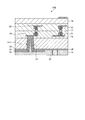
図1は、第1実施形態の容量素子を積層構造を有する半導体素子基板に適用した場合の部分断面図である。
半導体素子基板10は、第1シリコン(Si)基板11と、第1シリコン基板11の第1面(図中、下側の面)P1側に積層された半田レジスト層12と、第1シリコン基板11の第1面P1から第2面(図中、上側の面)P2側に貫通されてTSV(Through-Silicon-Via)として形成された第1貫通孔13-1に形成された容量素子14と、シリコン基板11の第1面P1側から第2面(図中、上側の面)P2側に貫通されてTSVとして形成された第2貫通孔13-2に形成されたシリコン貫通電極15と、第1シリコン基板11の第2面P2上に積層された第1絶縁体層16と、第1絶縁体層16に積層された第2絶縁体層17と、固体撮像素子が形成された第2シリコン基板18と、第1絶縁体層16内に形成され、容量素子14の一方の電極に接続された上部電極19と、第2絶縁体層17内に形成され、上部電極19に接続された第1配線20と、第1絶縁体層16内に形成され、シリコン貫通電極15に接続された下部電極21と、第2絶縁体層17内に形成され、下部電極21に接続された第2配線22と、を備えている。
図1は、第1実施形態の容量素子を積層構造を有する半導体素子基板に適用した場合の部分断面図である。
半導体素子基板10は、第1シリコン(Si)基板11と、第1シリコン基板11の第1面(図中、下側の面)P1側に積層された半田レジスト層12と、第1シリコン基板11の第1面P1から第2面(図中、上側の面)P2側に貫通されてTSV(Through-Silicon-Via)として形成された第1貫通孔13-1に形成された容量素子14と、シリコン基板11の第1面P1側から第2面(図中、上側の面)P2側に貫通されてTSVとして形成された第2貫通孔13-2に形成されたシリコン貫通電極15と、第1シリコン基板11の第2面P2上に積層された第1絶縁体層16と、第1絶縁体層16に積層された第2絶縁体層17と、固体撮像素子が形成された第2シリコン基板18と、第1絶縁体層16内に形成され、容量素子14の一方の電極に接続された上部電極19と、第2絶縁体層17内に形成され、上部電極19に接続された第1配線20と、第1絶縁体層16内に形成され、シリコン貫通電極15に接続された下部電極21と、第2絶縁体層17内に形成され、下部電極21に接続された第2配線22と、を備えている。
上記構成において、容量素子14は、上部電極19側を底側とみなした場合に、第1貫通孔13-1内において有底円筒形状を有し、第1シリコン基板11の第1面P1上で各部への配線がなされる第1導電膜層33と、容量素子14を構成する誘電体(絶縁体)として機能する誘電体層32と、第1導電膜層33に誘電体層32を介して対向するとともに、第1貫通孔13-1内において有底円筒形状を有し、第1シリコン基板11の第1面P1上で各部への配線及びシリコン貫通電極15への配線がなされる第2導電膜層31と、を備えている。
また、シリコン貫通電極15は、容量素子14と同様に、第1貫通孔13-2内において有底円筒形状を有し、第1シリコン基板11の第1面P1上で各部への配線がなされる第1導電膜層33を備えている。
ここで、容量素子14を構成している第1導電膜層33は、第1シリコン基板11の第1面P1側で上部電極19に電気的に接続され、シリコン貫通電極15を構成し、第2導電膜層31に接続されている第1導電膜層33は、第1シリコン基板11の第1面P1側で下部電極21に電気的に接続されている。
これらの結果、容量素子14は、第1導電膜層33及び第2導電膜層31で誘電体層32を挟んだ構成となる。したがって、容量素子14は、上部電極19と下部電極21との間、ひいては、第1配線20と第2配線22に接続されたコンデンサとして機能することとなる。
次に第1実施形態の容量素子の製造プロセスについて図2及び図3を参照して説明する。
図2は、第1実施形態の容量素子の製造プロセスの説明図(その1)である。
図3は、第1実施形態の容量素子の製造プロセスの説明図(その2)である。
図2は、第1実施形態の容量素子の製造プロセスの説明図(その1)である。
図3は、第1実施形態の容量素子の製造プロセスの説明図(その2)である。
以下の説明においては、第1シリコン基板11には、予めドライエッチング法等によりTSV(Through-Silicon-Via)としての第1貫通孔13-1及び第2貫通孔13-1が形成されているものとする。
さらに第1シリコン基板11の第2面P2上には、上部電極19及び下部電極21が形成された第1絶縁体層16が積層されているものとする。
さらに第1シリコン基板11の第2面P2上には、上部電極19及び下部電極21が形成された第1絶縁体層16が積層されているものとする。
上記状態において、図2(a)に示すように、まず、第1導電膜層33及び誘電体層32を形成する。
具体的には、例えば、第1シリコン基板11に対し、スパッタリング法によるチタン層形成、チタン層へのCVD(Chemical Vapor Deposition)法による銅層形成及び湿式RDL(Redistribution Layer)により第1導電膜層33を形成する。
具体的には、例えば、第1シリコン基板11に対し、スパッタリング法によるチタン層形成、チタン層へのCVD(Chemical Vapor Deposition)法による銅層形成及び湿式RDL(Redistribution Layer)により第1導電膜層33を形成する。
続いて、CVD法により誘電体層32としてのSiO層を形成し、電子ビーム(EB:Electron Beam)除去法により余分なSiO層を除去して所望形状を有する誘電体層32とする。
次に図2(b)に示すように、第2導電膜層31を形成する。
具体的には、例えば、第1導電膜層33の形成と同様に、第1シリコン基板11に対し、スパッタリング法によるチタン層形成、チタン層へのCVD法による銅層形成及び湿式RDLにより第2導電膜層31を形成する。
具体的には、例えば、第1導電膜層33の形成と同様に、第1シリコン基板11に対し、スパッタリング法によるチタン層形成、チタン層へのCVD法による銅層形成及び湿式RDLにより第2導電膜層31を形成する。
続いて、図2(c)に示すように、容量素子14を構成する第2導電膜層31を保護するように、フォトマスクMSKを配置する。
そして、図2(d)に示すように余分な第2導電膜層31を除去する。
具体的には、電子ビーム除去法等によりフォトマスクMSKが配置された部分以外の第2導電膜層31を除去する。
そして、図2(d)に示すように余分な第2導電膜層31を除去する。
具体的には、電子ビーム除去法等によりフォトマスクMSKが配置された部分以外の第2導電膜層31を除去する。
この結果、図2(c)のようにフォトマスクMSKを配置した場合には、図3(a)に示すように、第2導電膜層33のうち、誘電体層32に積層された部分及びシリコン貫通電極15を構成している第1導電膜層33と接続されている部分以外の第2導電膜層33が除去されている。
次に図3(b)に示すように、第2導電膜層31を電気的に絶縁し、物理的に保護するための絶縁体層41としてのSiO層をCVD法等により形成する。
続いて、図3(c)に示すように、容量素子14を構成する第2導電膜層31に積層された絶縁体層41を保護するように、再びフォトマスクMSKを配置する。
そして、図3(d)に示すように、余分な絶縁体層41を除去する。
具体的には、電子ビーム除去法等によりフォトマスクMSKが配置された部分以外の絶縁体層41を除去する。
この結果、図3(d)のようにフォトマスクMSKを配置した場合には、図3(e)に示すように、絶縁体層41のうち、第2導電膜層31に積層された部分以外の絶縁体層41が除去され、図1に示した容量素子14が形成されることとなる。
具体的には、電子ビーム除去法等によりフォトマスクMSKが配置された部分以外の絶縁体層41を除去する。
この結果、図3(d)のようにフォトマスクMSKを配置した場合には、図3(e)に示すように、絶縁体層41のうち、第2導電膜層31に積層された部分以外の絶縁体層41が除去され、図1に示した容量素子14が形成されることとなる。
本実施形態の容量素子14によれば、一つの容量素子のサイズを既存のTSVの径(数十~100μm)程度としても、十分な容量を確保することができる。
具体的には、TSVの径=60μm、TSV深さ=85μmとし、誘電体層32としてのSiOの厚さを40nmとした場合、以下の通りとなる。
TSVに対応するビアホール面積=60×85=18840μm2
とすると、TSV1個あたりの容量C=16pF程度となる。
具体的には、TSVの径=60μm、TSV深さ=85μmとし、誘電体層32としてのSiOの厚さを40nmとした場合、以下の通りとなる。
TSVに対応するビアホール面積=60×85=18840μm2
とすると、TSV1個あたりの容量C=16pF程度となる。
したがって、このような容量素子14をシリコン基板(上述の例の場合、第1シリコン基板11)内に複数形成することで、大容量の容量素子(群)を容易に構築できる。
また、上記構成によれば、容量素子14を絶縁基板(第1シリコン基板)に形成したTSV内に配置するとともに、従来使用されていなかった絶縁基板の裏面側(第1シリコン基板11の第1面P1側)の領域を容量素子14の配線に用いることで、既存の設計領域を圧迫すること無く、大規模容量素子を搭載することができ、対象回路のさらなる高集積化を実現できる。
[1.1]第1実施形態の第1変形例
次に第1実施形態の第1変形例の半導体素子について説明する。
図4は、第1実施形態の第1変形例の半導体素子の説明図である。
本変形例の半導体素子基板10Bが、第1実施形態の半導体素子基板10と異なる点は、第2導電膜層31をシリコン貫通電極15ではなく、導電膜層34を介して第1シリコン基板11の第1面P1側にフリップチップ接続用の電極端子として形成された銅ピラー37に接続した点である。
これにより、当該半導体素子基板10Bを図示しない外部の基板上に設ける場合でも実装面積の不要な増大を招くことなく電子機器を構築することができる。
以上の説明は、半導体素子基板10Bにピラー電極(銅ピラー37)を設ける場合で有ったが、バンプ電極を設けるようにし、容量素子14を構成している一対の電極のうち、いずれか他方をバンプ電極に接続するようにしてもよい。
次に第1実施形態の第1変形例の半導体素子について説明する。
図4は、第1実施形態の第1変形例の半導体素子の説明図である。
本変形例の半導体素子基板10Bが、第1実施形態の半導体素子基板10と異なる点は、第2導電膜層31をシリコン貫通電極15ではなく、導電膜層34を介して第1シリコン基板11の第1面P1側にフリップチップ接続用の電極端子として形成された銅ピラー37に接続した点である。
これにより、当該半導体素子基板10Bを図示しない外部の基板上に設ける場合でも実装面積の不要な増大を招くことなく電子機器を構築することができる。
以上の説明は、半導体素子基板10Bにピラー電極(銅ピラー37)を設ける場合で有ったが、バンプ電極を設けるようにし、容量素子14を構成している一対の電極のうち、いずれか他方をバンプ電極に接続するようにしてもよい。
[1.2]第1実施形態の第2変形例
次に第1実施形態の第2変形例の半導体素子について説明する。
図5は、第1実施形態の第2変形例の半導体素子の説明図である。
次に第1実施形態の第2変形例の半導体素子について説明する。
図5は、第1実施形態の第2変形例の半導体素子の説明図である。
本変形例の半導体素子基板10Cが、第1実施形態の半導体素子基板10と異なる点は、容量素子14と同様の複数の容量素子14-1~14-5を設け、容量素子14-1~14-5の第1導電膜層33を共通接続して、上部電極19に接続した点と、容量素子14-1~14-5の第2導電膜層33を共通接続して、シリコン貫通電極15を介して下部電極21に接続した点と、である。
このように構成することにより、容量素子14-1~14-5を並列接続した場合と等価となり、容量素子としての容量は、容量素子14-1~14-5の合成容量となり、容易に大容量の容量素子を構築できる。
より具体的には、第1実施形態の具体例で示した場合と同様に各容量素子14-1~14-5の容量が16pFであった場合、図5の第2変形例による容量素子14-1~14-5全体の容量は、16×5=80pFとなる。
このような構成とした場合も、製造プロセスは、第1実施形態の場合と同様となり、容易に大容量の容量素子(群)を得ることができる。
このような構成とした場合も、製造プロセスは、第1実施形態の場合と同様となり、容易に大容量の容量素子(群)を得ることができる。
[1.3]第1実施形態の具体例
次に第1実施形態の具体例について説明する。
図6は、第1実施形態の具体例の半導体素子基板における第1シリコン基板の外観図である。
半導体素子基板10を構成している第1シリコン基板11は、図6(a)のシリコン基板の第2面P2側からみた平面図に示すように、図中、砂地模様の領域ARには、部品配置領域あるいは配線配置領域は設けられていない。
次に第1実施形態の具体例について説明する。
図6は、第1実施形態の具体例の半導体素子基板における第1シリコン基板の外観図である。
半導体素子基板10を構成している第1シリコン基板11は、図6(a)のシリコン基板の第2面P2側からみた平面図に示すように、図中、砂地模様の領域ARには、部品配置領域あるいは配線配置領域は設けられていない。
そこで、本第1実施形態においては、図6(b)のシリコン基板の第1面P1側からみた平面図に示すように領域ARに対応する領域に複数(図6の場合、76個)の容量素子を形成している。
このように構成することにより、第1実施形態の具体例で示した場合のように、各容量素子14の容量が16pFであった場合、図6の場合における容量素子14全体の容量は、16×76=1216pFとなる。
同様の設置面積で、従来の方法で容量を形成した場合には、940pF程度となっており、充分に置き換えが可能となる。換言すれば、従来と同様の容量を確保しようとする場合には、半導体素子基板の設置面積をおよそ3%程度縮小することが可能となる。
したがって、本第1実施形態によれば、半導体素子基板ひいては、半導体素子基板を用いた電子機器の小型化を容易に図ることが可能となる。
したがって、本第1実施形態によれば、半導体素子基板ひいては、半導体素子基板を用いた電子機器の小型化を容易に図ることが可能となる。
[2]第2実施形態
図7は、第2実施形態の容量素子を積層構造を有する半導体素子基板に適用した場合の部分断面図である。
図7は、第2実施形態の容量素子を積層構造を有する半導体素子基板に適用した場合の部分断面図である。
第2実施形態の半導体素子基板100においては、第1実施形態の半導体素子基板10とは、第2絶縁体層17から上の構成は同様であるので、図示の簡略化のため、これらの図示を省略している。また、図7において、図1と同様の部分については、同一の符号を付すものとする。
第2実施形態の半導体素子基板100は、第1シリコン基板11と、第1シリコン基板11の第1面P1側に積層された半田レジスト層12と、シリコン基板11の第1面P1から第2面P2側に貫通されてTSVとして形成された第1貫通孔13-1に形成された容量素子14Aと、シリコン基板11の第1面P1から第2面(図中、上側の面)P2側に貫通されてTSVとして形成された第2貫通孔13-2に形成されたシリコン貫通電極15と、シリコン基板11の第2面P2上に積層された第1絶縁体層16と、第1絶縁体層16に積層された第2絶縁体層17と、固体撮像素子が形成された第2シリコン基板18と、第1絶縁体層16内に形成され、容量素子14の一方の電極に接続された上部電極19と、第2絶縁体層17内に形成され、シリコン貫通電極15に接続された下部電極21と、を備えている。
上記構成において、容量素子14Aは、上部電極19側を底側とみなした場合に、第1貫通孔13-1内において有底円筒形状を有し、第1シリコン基板11の第1面P1上で各部への配線がなされる第1の電極(電極A)を構成する導電膜層33に電気的に接続されている第1導電膜層33-1と、容量素子14を構成する誘電体(絶縁体)として機能する第1誘電体層32-1と、第1導電膜層33-1に第1誘電体層32-1を介して対向するとともに、第1貫通孔13-1内において有底円筒形状を有し、第1シリコン基板11の第1面P1上で各部への配線及びシリコン貫通電極15への配線がなされる第2の電極(電極B)を構成する導電膜層34に電気的に接続されている第2導電膜層34-1と、容量素子14を構成する誘電体(絶縁体)として機能する第2誘電体層32-2と、を備えている。
また、容量素子14Aは、第2導電膜層33-2に第2誘電体層32-2を介して対向するとともに、第1貫通孔13-1内において有底円筒形状を有し、第1シリコン基板11の第1面P1上で各部への配線がなされる第1の電極(電極A)を構成する導電膜層33に電気的に接続されている第3導電膜層34-2と、容量素子14を構成する誘電体(絶縁体)として機能する第3誘電体層32-3と、を備えている。
さらに、容量素子14Aは、第3導電膜層33-2に第3誘電体層32-3を介して対向するとともに、第1貫通孔13-1内において有底円筒形状を有し、第1シリコン基板11の第1面P1上で各部への配線及びシリコン貫通電極15への配線がなされる第2の電極(電極B)を構成する導電膜層34に電気的に接続されている第4導電膜層34-2を備えている。
上記構成において、容量素子14Aは、上部電極19側を底側とみなした場合に、第1貫通孔13-1内において有底円筒形状を有し、第1シリコン基板11の第1面P1上で各部への配線がなされる第1の電極(電極A)を構成する導電膜層33に電気的に接続されている第1導電膜層33-1と、容量素子14を構成する誘電体(絶縁体)として機能する第1誘電体層32-1と、第1導電膜層33-1に第1誘電体層32-1を介して対向するとともに、第1貫通孔13-1内において有底円筒形状を有し、第1シリコン基板11の第1面P1上で各部への配線及びシリコン貫通電極15への配線がなされる第2の電極(電極B)を構成する導電膜層34に電気的に接続されている第2導電膜層34-1と、容量素子14を構成する誘電体(絶縁体)として機能する第2誘電体層32-2と、を備えている。
また、容量素子14Aは、第2導電膜層33-2に第2誘電体層32-2を介して対向するとともに、第1貫通孔13-1内において有底円筒形状を有し、第1シリコン基板11の第1面P1上で各部への配線がなされる第1の電極(電極A)を構成する導電膜層33に電気的に接続されている第3導電膜層34-2と、容量素子14を構成する誘電体(絶縁体)として機能する第3誘電体層32-3と、を備えている。
さらに、容量素子14Aは、第3導電膜層33-2に第3誘電体層32-3を介して対向するとともに、第1貫通孔13-1内において有底円筒形状を有し、第1シリコン基板11の第1面P1上で各部への配線及びシリコン貫通電極15への配線がなされる第2の電極(電極B)を構成する導電膜層34に電気的に接続されている第4導電膜層34-2を備えている。
また、シリコン貫通電極15は、第1実施形態と同様に、第1貫通孔13-2内において有底円筒形状を有し、第1シリコン基板11の第1面P1上で各部への配線がなされる導電膜層34を備えている。
ここで、容量素子14Aを構成している第1導電膜層33-1、ひいては、第3導電膜層33-2及び導電膜層33は、第1シリコン基板11の第1面P1側で上部電極19に電気的に接続されている。
また、シリコン貫通電極15を構成し、導電膜層34に接続されている第2導電膜層34-1、ひいては、第4導電膜層34-2は、第1シリコン基板11の第1面P1側で下部電極21に電気的に接続されている。
これらの結果、容量素子14Aは、第1導電膜層33-1及び第2導電膜層34-1で第1誘電体層32-1を挟み、第2導電膜層33-2及び第3導電膜層33-2で第2誘電体層32-2を挟み、第3導電膜層34-1及び第4導電膜層34-2で第3誘電体層32-3を挟んだ構成となる。
すなわち、容量素子14Aは、上部電極19と下部電極21との間、ひいては、第1配線20と第2配線に接続された3個の並列接続されたコンデンサとして機能することとなる。
また、シリコン貫通電極15を構成し、導電膜層34に接続されている第2導電膜層34-1、ひいては、第4導電膜層34-2は、第1シリコン基板11の第1面P1側で下部電極21に電気的に接続されている。
これらの結果、容量素子14Aは、第1導電膜層33-1及び第2導電膜層34-1で第1誘電体層32-1を挟み、第2導電膜層33-2及び第3導電膜層33-2で第2誘電体層32-2を挟み、第3導電膜層34-1及び第4導電膜層34-2で第3誘電体層32-3を挟んだ構成となる。
すなわち、容量素子14Aは、上部電極19と下部電極21との間、ひいては、第1配線20と第2配線に接続された3個の並列接続されたコンデンサとして機能することとなる。
本第2実施形態によれば、第1実施形態と比較して容量素子14Aとしての極板面積は、実効的に3倍程度となっているので、容量もおよそ3倍となっている。したがって、第1実施形態の具体例で示した場合のように、各容量素子14の容量が16pFであった場合、図6の場合における容量素子14A全体の容量は、16×76×3=3648pFとなる。
上述したように、同様の設置面積で、従来の方法で容量を形成した場合には、940pF程度となっているので、従来と同様の容量を確保しようとする場合には、半導体素子基板の設置面積をおよそ30%程度縮小することが可能となる。
したがって、本第2実施形態によれば、第1実施形態と比較して、同一の設置面積で、より大きな容量の容量素子を形成することができ、半導体素子基板ひいては、半導体素子基板を用いた電子機器のより一層の小型化を容易に図ることが可能となる。
したがって、本第2実施形態によれば、第1実施形態と比較して、同一の設置面積で、より大きな容量の容量素子を形成することができ、半導体素子基板ひいては、半導体素子基板を用いた電子機器のより一層の小型化を容易に図ることが可能となる。
以上の説明は、3個の並列接続されたコンデンサとして機能させる場合であったが、第3誘電体層32-3及び第4導電膜層34-2を設けない構成とすれば、2個の並列接続されたコンデンサとして機能させることができ、さらには、製造工程の許す限り4個の並列接続されたコンデンサとして機能させることも可能である。
[3]第3実施形態
図8は、第3実施形態の容量素子を積層構造を有する半導体素子基板に適用した場合の部分断面図である。
図8は、第3実施形態の容量素子を積層構造を有する半導体素子基板に適用した場合の部分断面図である。
第3実施形態の半導体素子基板10Eにおいては、第2実施形態と同様に、第1実施形態の半導体素子基板10とは、第2絶縁体層17から上の構成は同様であるので、図示の簡略化のため、これらの図示を省略している。また、図8において、図1と同様の部分については、同一の符号を付すものとする。
第3実施形態の半導体素子基板10Eが、第1実施形態の半導体素子基板10と異なる点は、第1シリコン基板11及び第1絶縁体層16と、容量素子14Bあるいはシリコン貫通電極15Bとの間に第3絶縁体層51を設けた点である。
本第3実施形態によれば、第1貫通孔13-1の内周面を第1貫通孔13-1を単にドライエッチング法等により形成した場合と比較して平滑化することができ、その後の容量素子形成における処理の安定性、ひいては、形成した容量素子の容量の変動を抑制することができる。
本第3実施形態によれば、第1貫通孔13-1の内周面を第1貫通孔13-1を単にドライエッチング法等により形成した場合と比較して平滑化することができ、その後の容量素子形成における処理の安定性、ひいては、形成した容量素子の容量の変動を抑制することができる。
次に第3実施形態の容量素子の製造プロセスについて図9及び図10を参照して説明する。
図9は、第3実施形態の容量素子の製造プロセスの説明図(その1)である。
図10は、第3実施形態の容量素子の製造プロセスの説明図(その2)である。
以下の説明においては、第1シリコン基板11には、予めドライエッチング法等によりTSV(Through-Silicon-Via)としての第1貫通孔13-1及び第2貫通孔13-1が形成されているものとする。
さらに第1シリコン基板11の第2面P2上には、上部電極19及び下部電極21が形成された第1絶縁体層16、第1配線20及び第2配線22が形成された第2絶縁体層17及び固体撮像素子が形成された第2シリコン基板18と、が積層されているものとする。
図9は、第3実施形態の容量素子の製造プロセスの説明図(その1)である。
図10は、第3実施形態の容量素子の製造プロセスの説明図(その2)である。
以下の説明においては、第1シリコン基板11には、予めドライエッチング法等によりTSV(Through-Silicon-Via)としての第1貫通孔13-1及び第2貫通孔13-1が形成されているものとする。
さらに第1シリコン基板11の第2面P2上には、上部電極19及び下部電極21が形成された第1絶縁体層16、第1配線20及び第2配線22が形成された第2絶縁体層17及び固体撮像素子が形成された第2シリコン基板18と、が積層されているものとする。
上記状態において、図9(a)に示すように、まず、第3絶縁体層51を形成する。
具体的には、第3絶縁体層51としてのSiO層をCVD法等により形成する。
続いて、図9(b)に示すように、第1導電膜層33を形成する。
具体的には、例えば、第1シリコン基板11に対し、スパッタリング法によるチタン層形成、チタン層へのCVD法による銅層形成及び湿式RDLにより第1導電膜層33を形成する。
具体的には、第3絶縁体層51としてのSiO層をCVD法等により形成する。
続いて、図9(b)に示すように、第1導電膜層33を形成する。
具体的には、例えば、第1シリコン基板11に対し、スパッタリング法によるチタン層形成、チタン層へのCVD法による銅層形成及び湿式RDLにより第1導電膜層33を形成する。
さらに図9(c)に示すように、誘電体層32を形成する。
具体的には、CVD法により誘電体層32としてのSiO層を形成する。
次に、図10(a)に示すように、余分なSiO層を除去して所望形状を有する誘電体層32を形成する。
具体的には、誘電体層32に電子ビームを照射して除去する電子ビーム除去法により余分なSiO層を除去して所望形状を有する誘電体層32とする。
具体的には、CVD法により誘電体層32としてのSiO層を形成する。
次に、図10(a)に示すように、余分なSiO層を除去して所望形状を有する誘電体層32を形成する。
具体的には、誘電体層32に電子ビームを照射して除去する電子ビーム除去法により余分なSiO層を除去して所望形状を有する誘電体層32とする。
次に図10(b)に示すように、第2導電膜層33を形成する。
具体的には、例えば、第1導電膜層33の形成と同様に、第1シリコン基板11に対し、スパッタリング法によるチタン層形成、チタン層へのCVD法による銅層形成及び湿式RDLにより第2導電膜層31を形成する。
具体的には、例えば、第1導電膜層33の形成と同様に、第1シリコン基板11に対し、スパッタリング法によるチタン層形成、チタン層へのCVD法による銅層形成及び湿式RDLにより第2導電膜層31を形成する。
続いて、図10(c)に示すように、半田レジスト層12を第1シリコン基板11の第1面(図中、下側の面)P1側に積層して形成する。
具体的には、印刷法により、半田レジスト層12を形成する。
この結果、図8に示した第3実施形態の容量素子14が形成された半導体素子基板が得られる。
具体的には、印刷法により、半田レジスト層12を形成する。
この結果、図8に示した第3実施形態の容量素子14が形成された半導体素子基板が得られる。
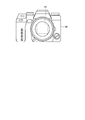
図11は、上記各実施形態の容量素子及び半導体素子基板が適用された電子機器としてのディジタルスチルカメラの外観図である。
電子機器としてのレンズ交換式一眼レフレックスタイプのディジタルスチルカメラのカメラ本体部(カメラボディ)50は、撮像装置として上述した容量素子14を有する半導体素子基板(例えば、CMOSイメージセンサ基板)を備えた半導体素子基板10を内蔵している。
このような構成とすることにより、電子機器の安定動作を図り、小型化を容易とすることができる。
以上、実施の形態および変形例を挙げて本技術を説明したが、本技術は上記実施の形態等に限定されるものではなく、種々変形が可能である。
例えば、上記説明においては、容量素子が電源回路を構成するチャージポンプ回路を例として説明したが、大容量の容量素子が要求される回路を備えた半導体素子基板であれば同様に適用が可能である。
また以上の説明は、容量素子を並列に接続した場合について説明したが、容量調整など必要に応じて少なくとも一部の容量素子を直列に接続するように配線を行うことも可能である。
以上の説明においては、絶縁層の材料として、SiO2を用いる場合について説明したが、絶縁層の材料としてSiN等の他の絶縁材料を用いることも可能である。
以上の説明においては、容量素子のいずれかの導電層として、シリコン貫通電極と同一の導電材料を用いていたが、異なる導電材料を用いるように構成することも可能である。
また以上の説明は、容量素子を並列に接続した場合について説明したが、容量調整など必要に応じて少なくとも一部の容量素子を直列に接続するように配線を行うことも可能である。
以上の説明においては、絶縁層の材料として、SiO2を用いる場合について説明したが、絶縁層の材料としてSiN等の他の絶縁材料を用いることも可能である。
以上の説明においては、容量素子のいずれかの導電層として、シリコン貫通電極と同一の導電材料を用いていたが、異なる導電材料を用いるように構成することも可能である。
[5]実施形態の効果
以上の説明のように、本実施形態によれば、容量素子を絶縁基板に形成した貫通孔(TSV)内に配置するとともに、従来使用されていなかった絶縁基板の裏面側の領域を容量素子の配線に用いた半導体素子基板を構成することで、既存の設計領域を圧迫すること無く、大規模容量素子を搭載することができ、対象回路のさらなる高集積化を実現できる。ひいては、対象回路を用いた電子回路の小型化を容易に図ることができる。
以上の説明のように、本実施形態によれば、容量素子を絶縁基板に形成した貫通孔(TSV)内に配置するとともに、従来使用されていなかった絶縁基板の裏面側の領域を容量素子の配線に用いた半導体素子基板を構成することで、既存の設計領域を圧迫すること無く、大規模容量素子を搭載することができ、対象回路のさらなる高集積化を実現できる。ひいては、対象回路を用いた電子回路の小型化を容易に図ることができる。
なお、本明細書に記載された効果はあくまで例示であって限定されるものでは無く、また他の効果があってもよい。
なお、本技術は以下のような構成も採ることができる。
(1)
絶縁体基板の第1面から反対側の第2面に貫通するように形成された貫通孔の内周面において互いに対向するように配置された複数の導電膜層と、
対向する一対の導電膜層間に形成された誘電体層と、を備え、
前記複数の導電膜層のうち、いずれか少なくとも一つが容量素子を構成する一対の電極のうちいずれか一方として前記第2面側に形成された回路配線に接続可能とされている、
容量素子。
(2)
前記導電膜層は、少なくとも三つ以上設けられており、
二つの前記誘電体層及び一つの前記導電膜層を介して配置された前記導電膜層同士は、共通接続されている、(1)記載の容量素子。
(3)
前記貫通孔と最外周側に形成された前記導電膜層との間に形成された絶縁体層を備えた、(1)または(2)記載の容量素子。
(4)
絶縁体基板と、
前記絶縁体基板の第1面から反対側の第2面に貫通するように形成された貫通孔の内周面において互いに対向するように配置された複数の導電膜層と、対向する一対の導電膜層間に形成された誘電体層と、を有する容量素子と、備え、
前記複数の導電膜層のうち、いずれか少なくとも一つが容量素子を構成する一対の電極のうちいずれか一方として前記第2面側に形成された回路配線に接続されている、
半導体素子基板。
(5)
前記導電膜層は、少なくとも三つ以上設けられており、
二つの前記誘電体層及び一つの前記導電膜層を介して配置された前記導電膜層同士は、共通接続されている、(4)記載の半導体素子基板。
(6)
前記半導体素子基板は、前記絶縁体基板に設けられた貫通電極、ピラー電極あるいはバンプ電極を有し、
前記容量素子を構成している前記一対の電極のうち、いずれか他方は、前記絶縁体基板に設けられた貫通電極、ピラー電極あるいはバンプ電極に接続されている、(4)または(5)記載の半導体素子基板。
(7)
前記絶縁体基板には、複数の前記貫通孔が設けられており、前記複数の貫通孔内に前記容量素子がそれぞれ形成され、一の前記容量素子の電極のいずれか一方は、他の前記容量素子の電極のいずれか他方に共通接続されている、(4)乃至(6)のいずれかに記載の半導体素子基板。
(8)
前記絶縁体基板に積層された第2の絶縁体基板を有し、前記容量素子は、前記貫通孔を介して前記第2の絶縁体基板に形成された回路配線に電極が接続されている、(4)乃至(7)のいずれかに記載の半導体素子基板。
(9)
絶縁体基板と、
前記絶縁体基板の第1面から反対側の第2面に貫通するように形成された貫通孔の内周面において互いに対向するように配置された複数の導電膜層と、対向する一対の導電膜層間に形成された誘電体層と、を備え、前記複数の導電膜層のうち、いずれか少なくとも一つが容量素子を構成する一対の電極のうちいずれか一方として前記第2面側に形成された回路配線に接続可能とされた容量素子を有する電子回路を備えた電子機器。
(10)
容量素子において、前記導電膜層は、少なくとも三つ以上設けられており、
二つの前記誘電体層及び一つの導電膜層を介して配置された前記導電膜層同士は、共通接続されている、(9)記載の電子機器。
(11)
前記貫通孔と最外周側に形成された前記導電膜層との間に形成された絶縁体層を備えた、(9)または(10)記載の電子機器。
(12)
絶縁体基板と、前記絶縁体基板の第1面から反対側の第2面に貫通するように形成された貫通孔の内周面において互いに対向するように配置された複数の導電膜層と、対向する一対の導電膜層間に形成された誘電体層と、を有する容量素子と、備え、前記複数の導電膜層のうち、いずれか少なくとも一つが容量素子を構成する一対の電極のうちいずれか一方として前記第2面側に形成された回路配線に接続されている半導体素子基板を有する電子回路を備えた電子機器。
(13)
前記半導体素子基板において、前記導電膜層は、少なくとも三つ以上設けられており、
二つの前記誘電体層及び一つの導電膜層を介して配置された前記導電膜層同士は、共通接続されている、(12)記載の電子機器。
(14)
前記半導体素子基板は、前記絶縁体基板に設けられた貫通電極、ピラー電極あるいはバンプ電極を有し、
前記容量素子を構成している前記一対の電極のうち、いずれか他方は、前記絶縁体基板に設けられた貫通電極、ピラー電極あるいはバンプ電極に接続されている、(12)または(13)記載の電子機器。
(15)
前記絶縁体基板には、複数の前記貫通孔が設けられており、前記複数の貫通孔内に前記容量素子がそれぞれ形成され、一の前記容量素子の電極のいずれか一方は、他の前記容量素子の電極のいずれか他方に共通接続されている、(12)乃至(14)のいずれかに記載の電子機器。
(16)
前記絶縁体基板に積層された第2の絶縁体基板を有し、前記容量素子は、前記貫通孔を介して前記第2の絶縁体基板に形成された回路配線に電極が接続されている、(12)乃至(15)のいずれかに記載の電子機器。
(1)
絶縁体基板の第1面から反対側の第2面に貫通するように形成された貫通孔の内周面において互いに対向するように配置された複数の導電膜層と、
対向する一対の導電膜層間に形成された誘電体層と、を備え、
前記複数の導電膜層のうち、いずれか少なくとも一つが容量素子を構成する一対の電極のうちいずれか一方として前記第2面側に形成された回路配線に接続可能とされている、
容量素子。
(2)
前記導電膜層は、少なくとも三つ以上設けられており、
二つの前記誘電体層及び一つの前記導電膜層を介して配置された前記導電膜層同士は、共通接続されている、(1)記載の容量素子。
(3)
前記貫通孔と最外周側に形成された前記導電膜層との間に形成された絶縁体層を備えた、(1)または(2)記載の容量素子。
(4)
絶縁体基板と、
前記絶縁体基板の第1面から反対側の第2面に貫通するように形成された貫通孔の内周面において互いに対向するように配置された複数の導電膜層と、対向する一対の導電膜層間に形成された誘電体層と、を有する容量素子と、備え、
前記複数の導電膜層のうち、いずれか少なくとも一つが容量素子を構成する一対の電極のうちいずれか一方として前記第2面側に形成された回路配線に接続されている、
半導体素子基板。
(5)
前記導電膜層は、少なくとも三つ以上設けられており、
二つの前記誘電体層及び一つの前記導電膜層を介して配置された前記導電膜層同士は、共通接続されている、(4)記載の半導体素子基板。
(6)
前記半導体素子基板は、前記絶縁体基板に設けられた貫通電極、ピラー電極あるいはバンプ電極を有し、
前記容量素子を構成している前記一対の電極のうち、いずれか他方は、前記絶縁体基板に設けられた貫通電極、ピラー電極あるいはバンプ電極に接続されている、(4)または(5)記載の半導体素子基板。
(7)
前記絶縁体基板には、複数の前記貫通孔が設けられており、前記複数の貫通孔内に前記容量素子がそれぞれ形成され、一の前記容量素子の電極のいずれか一方は、他の前記容量素子の電極のいずれか他方に共通接続されている、(4)乃至(6)のいずれかに記載の半導体素子基板。
(8)
前記絶縁体基板に積層された第2の絶縁体基板を有し、前記容量素子は、前記貫通孔を介して前記第2の絶縁体基板に形成された回路配線に電極が接続されている、(4)乃至(7)のいずれかに記載の半導体素子基板。
(9)
絶縁体基板と、
前記絶縁体基板の第1面から反対側の第2面に貫通するように形成された貫通孔の内周面において互いに対向するように配置された複数の導電膜層と、対向する一対の導電膜層間に形成された誘電体層と、を備え、前記複数の導電膜層のうち、いずれか少なくとも一つが容量素子を構成する一対の電極のうちいずれか一方として前記第2面側に形成された回路配線に接続可能とされた容量素子を有する電子回路を備えた電子機器。
(10)
容量素子において、前記導電膜層は、少なくとも三つ以上設けられており、
二つの前記誘電体層及び一つの導電膜層を介して配置された前記導電膜層同士は、共通接続されている、(9)記載の電子機器。
(11)
前記貫通孔と最外周側に形成された前記導電膜層との間に形成された絶縁体層を備えた、(9)または(10)記載の電子機器。
(12)
絶縁体基板と、前記絶縁体基板の第1面から反対側の第2面に貫通するように形成された貫通孔の内周面において互いに対向するように配置された複数の導電膜層と、対向する一対の導電膜層間に形成された誘電体層と、を有する容量素子と、備え、前記複数の導電膜層のうち、いずれか少なくとも一つが容量素子を構成する一対の電極のうちいずれか一方として前記第2面側に形成された回路配線に接続されている半導体素子基板を有する電子回路を備えた電子機器。
(13)
前記半導体素子基板において、前記導電膜層は、少なくとも三つ以上設けられており、
二つの前記誘電体層及び一つの導電膜層を介して配置された前記導電膜層同士は、共通接続されている、(12)記載の電子機器。
(14)
前記半導体素子基板は、前記絶縁体基板に設けられた貫通電極、ピラー電極あるいはバンプ電極を有し、
前記容量素子を構成している前記一対の電極のうち、いずれか他方は、前記絶縁体基板に設けられた貫通電極、ピラー電極あるいはバンプ電極に接続されている、(12)または(13)記載の電子機器。
(15)
前記絶縁体基板には、複数の前記貫通孔が設けられており、前記複数の貫通孔内に前記容量素子がそれぞれ形成され、一の前記容量素子の電極のいずれか一方は、他の前記容量素子の電極のいずれか他方に共通接続されている、(12)乃至(14)のいずれかに記載の電子機器。
(16)
前記絶縁体基板に積層された第2の絶縁体基板を有し、前記容量素子は、前記貫通孔を介して前記第2の絶縁体基板に形成された回路配線に電極が接続されている、(12)乃至(15)のいずれかに記載の電子機器。
10 半導体素子基板
10B~10E 半導体素子基板
11 第1シリコン基板
12 半田レジスト層
13-1 第2貫通孔
13-2 第1貫通孔
14、14A、14B 容量素子
15、15B シリコン貫通電極
16 第1絶縁体層
17 第2絶縁体層
18 第2シリコン基板
19 上部電極
20 第1配線
21 下部電極
22 第2配線
31 第2導電膜層
32-1 第1誘電体層
32-2 第2誘電体層
32-3 第3誘電体層
33 導電膜層
33-1 第1導電膜層
33-2 第3導電膜層
34 導電膜層
34-1 第2導電膜層
34-2 第4導電膜層
37 銅ピラー
41 絶縁体層
51 第3絶縁体層
100 半導体素子基板
AR 領域
P1 第1面
P2 第2面
10B~10E 半導体素子基板
11 第1シリコン基板
12 半田レジスト層
13-1 第2貫通孔
13-2 第1貫通孔
14、14A、14B 容量素子
15、15B シリコン貫通電極
16 第1絶縁体層
17 第2絶縁体層
18 第2シリコン基板
19 上部電極
20 第1配線
21 下部電極
22 第2配線
31 第2導電膜層
32-1 第1誘電体層
32-2 第2誘電体層
32-3 第3誘電体層
33 導電膜層
33-1 第1導電膜層
33-2 第3導電膜層
34 導電膜層
34-1 第2導電膜層
34-2 第4導電膜層
37 銅ピラー
41 絶縁体層
51 第3絶縁体層
100 半導体素子基板
AR 領域
P1 第1面
P2 第2面
Claims (10)
- 絶縁体基板の第1面から反対側の第2面に貫通するように形成された貫通孔の内周面において互いに対向するように配置された複数の導電膜層と、
対向する一対の導電膜層間に形成された誘電体層と、を備え、
前記複数の導電膜層のうち、いずれか少なくとも一つが容量素子を構成する一対の電極のうちいずれか一方として前記第2面側に形成された回路配線に接続可能とされている、
容量素子。 - 前記導電膜層は、少なくとも三つ以上設けられており、
二つの前記誘電体層及び一つの前記導電膜層を介して配置された前記導電膜層同士は、共通接続されている、
請求項1記載の容量素子。 - 前記貫通孔と最外周側に形成された前記導電膜層との間に形成された絶縁体層を備えた、
請求項1記載の容量素子。 - 絶縁体基板と、
前記絶縁体基板の第1面から反対側の第2面に貫通するように形成された貫通孔の内周面において互いに対向するように配置された複数の導電膜層と、対向する一対の導電膜層間に形成された誘電体層と、を有する容量素子と、備え、
前記複数の導電膜層のうち、いずれか少なくとも一つが容量素子を構成する一対の電極のうちいずれか一方として前記第2面側に形成された回路配線に接続されている、
半導体素子基板。 - 前記導電膜層は、少なくとも三つ以上設けられており、
二つの前記誘電体層及び一つの前記導電膜層を介して配置された前記導電膜層同士は、共通接続されている、
請求項4記載の半導体素子基板。 - 前記半導体素子基板は、前記絶縁体基板に設けられた貫通電極、ピラー電極あるいはバンプ電極を有し、
前記容量素子を構成している前記一対の電極のうち、いずれか他方は、前記絶縁体基板に設けられた貫通電極、ピラー電極あるいはバンプ電極に接続されている、
請求項4記載の半導体素子基板。 - 前記絶縁体基板には、複数の前記貫通孔が設けられており、前記複数の貫通孔内に前記容量素子がそれぞれ形成され、一の前記容量素子の電極のいずれか一方は、他の前記容量素子の電極のいずれか他方に共通接続されている、
請求項4記載の半導体素子基板。 - 前記絶縁体基板に積層された第2の絶縁体基板を有し、前記容量素子は、前記貫通孔を介して前記第2の絶縁体基板に形成された回路配線に電極が接続されている、
請求項4記載の半導体素子基板。 - 絶縁体基板と、
前記絶縁体基板の第1面から反対側の第2面に貫通するように形成された貫通孔の内周面において互いに対向するように配置された複数の導電膜層と、対向する一対の導電膜層間に形成された誘電体層と、を備え、前記複数の導電膜層のうち、いずれか少なくとも一つが容量素子を構成する一対の電極のうちいずれか一方として前記第2面側に形成された回路配線に接続可能とされた容量素子を有する電子回路を備えた電子機器。 - 絶縁体基板と、前記絶縁体基板の第1面から反対側の第2面に貫通するように形成された貫通孔の内周面において互いに対向するように配置された複数の導電膜層と、対向する一対の導電膜層間に形成された誘電体層と、を有する容量素子と、備え、前記複数の導電膜層のうち、いずれか少なくとも一つが容量素子を構成する一対の電極のうちいずれか一方として前記第2面側に形成された回路配線に接続されている半導体素子基板を有する電子回路を備えた電子機器。
Applications Claiming Priority (2)
| Application Number | Priority Date | Filing Date | Title |
|---|---|---|---|
| JP2019037386A JP2020141090A (ja) | 2019-03-01 | 2019-03-01 | 容量素子、半導体素子基板及び電子機器 |
| JP2019-037386 | 2019-03-01 |
Publications (1)
| Publication Number | Publication Date |
|---|---|
| WO2020179452A1 true WO2020179452A1 (ja) | 2020-09-10 |
Family
ID=72280581
Family Applications (1)
| Application Number | Title | Priority Date | Filing Date |
|---|---|---|---|
| PCT/JP2020/006552 Ceased WO2020179452A1 (ja) | 2019-03-01 | 2020-02-19 | 容量素子、半導体素子基板及び電子機器 |
Country Status (2)
| Country | Link |
|---|---|
| JP (1) | JP2020141090A (ja) |
| WO (1) | WO2020179452A1 (ja) |
Cited By (2)
| Publication number | Priority date | Publication date | Assignee | Title |
|---|---|---|---|---|
| WO2024024933A1 (ja) * | 2022-07-29 | 2024-02-01 | ソニーセミコンダクタソリューションズ株式会社 | 半導体装置およびその製造方法、並びに電子機器 |
| EP4614572A4 (en) * | 2022-11-04 | 2026-01-21 | Sony Semiconductor Solutions Corp | ELECTRONIC DEVICE |
Families Citing this family (1)
| Publication number | Priority date | Publication date | Assignee | Title |
|---|---|---|---|---|
| JP2024044280A (ja) | 2022-09-21 | 2024-04-02 | ソニーセミコンダクタソリューションズ株式会社 | 電子デバイスおよび電子デバイスの製造方法 |
Citations (7)
| Publication number | Priority date | Publication date | Assignee | Title |
|---|---|---|---|---|
| JPH0897375A (ja) * | 1994-07-26 | 1996-04-12 | Toshiba Corp | マイクロ波集積回路装置及びその製造方法 |
| JPH0897367A (ja) * | 1994-09-27 | 1996-04-12 | Murata Mfg Co Ltd | 半導体装置 |
| JPH11195751A (ja) * | 1997-12-29 | 1999-07-21 | Nec Corp | コンデンサを備えた半導体装置 |
| JP2008288309A (ja) * | 2007-05-16 | 2008-11-27 | Sony Corp | 半導体装置及びその製造方法 |
| JP2015503228A (ja) * | 2011-11-16 | 2015-01-29 | クアルコム,インコーポレイテッド | 絶縁層および第2の層を有する積層されたチップセットおよびそれを形成する方法 |
| JP2015041677A (ja) * | 2013-08-21 | 2015-03-02 | ルネサスエレクトロニクス株式会社 | 半導体装置およびその製造方法 |
| JP2017513218A (ja) * | 2014-03-25 | 2017-05-25 | アイピーディーアイエイ | コンデンサ構造 |
-
2019
- 2019-03-01 JP JP2019037386A patent/JP2020141090A/ja active Pending
-
2020
- 2020-02-19 WO PCT/JP2020/006552 patent/WO2020179452A1/ja not_active Ceased
Patent Citations (7)
| Publication number | Priority date | Publication date | Assignee | Title |
|---|---|---|---|---|
| JPH0897375A (ja) * | 1994-07-26 | 1996-04-12 | Toshiba Corp | マイクロ波集積回路装置及びその製造方法 |
| JPH0897367A (ja) * | 1994-09-27 | 1996-04-12 | Murata Mfg Co Ltd | 半導体装置 |
| JPH11195751A (ja) * | 1997-12-29 | 1999-07-21 | Nec Corp | コンデンサを備えた半導体装置 |
| JP2008288309A (ja) * | 2007-05-16 | 2008-11-27 | Sony Corp | 半導体装置及びその製造方法 |
| JP2015503228A (ja) * | 2011-11-16 | 2015-01-29 | クアルコム,インコーポレイテッド | 絶縁層および第2の層を有する積層されたチップセットおよびそれを形成する方法 |
| JP2015041677A (ja) * | 2013-08-21 | 2015-03-02 | ルネサスエレクトロニクス株式会社 | 半導体装置およびその製造方法 |
| JP2017513218A (ja) * | 2014-03-25 | 2017-05-25 | アイピーディーアイエイ | コンデンサ構造 |
Cited By (2)
| Publication number | Priority date | Publication date | Assignee | Title |
|---|---|---|---|---|
| WO2024024933A1 (ja) * | 2022-07-29 | 2024-02-01 | ソニーセミコンダクタソリューションズ株式会社 | 半導体装置およびその製造方法、並びに電子機器 |
| EP4614572A4 (en) * | 2022-11-04 | 2026-01-21 | Sony Semiconductor Solutions Corp | ELECTRONIC DEVICE |
Also Published As
| Publication number | Publication date |
|---|---|
| JP2020141090A (ja) | 2020-09-03 |
Similar Documents
| Publication | Publication Date | Title |
|---|---|---|
| TWI578455B (zh) | 在封裝體基體中整合嵌入式薄膜電容器之技術 | |
| US10262967B2 (en) | Semiconductor packages | |
| TWI400731B (zh) | 電容元件及其製造方法 | |
| JP7052824B2 (ja) | 薄膜型lc部品およびその実装構造 | |
| CN115997263B (zh) | 薄膜电容器及其制造方法、以及具备薄膜电容器的电子电路基板 | |
| JP6669513B2 (ja) | 回路基板および回路基板の製造方法 | |
| WO2020179452A1 (ja) | 容量素子、半導体素子基板及び電子機器 | |
| US11621128B2 (en) | Capacitor unit | |
| TWI524505B (zh) | 半導體裝置及其製造方法 | |
| TW200414835A (en) | Integrated storage plate with embedded passive components and method for fabricating electronic device with the plate | |
| WO2013120378A1 (zh) | Mom电容器及其制作方法 | |
| JP2006185935A (ja) | キャパシタ部品 | |
| CN100468731C (zh) | 半导体叠层电容器 | |
| TWI669997B (zh) | 線路板結構及其製作方法 | |
| US9640477B1 (en) | Semiconductor package and method of producing the semiconductor package | |
| CN105575945A (zh) | 一种mom电容及其制作方法 | |
| CN102169860A (zh) | 具有被动组件结构的半导体结构及其制造方法 | |
| KR101846388B1 (ko) | 수직구조 캐패시터 및 수직구조 캐패시터의 형성 방법 | |
| CN108550531B (zh) | 封装基板的制造方法 | |
| TWI860117B (zh) | 半導體結構及其製造方法 | |
| CN119153232B (zh) | 电容芯片结构以及制造方法 | |
| CN115064524B (zh) | 导电孔阵列电容、制备方法、芯片、制备方法和电子设备 | |
| EP4489071B1 (en) | Semiconductor device including semiconductor package with capacitor embedded in dielectric layer | |
| JP2017212431A (ja) | キャパシタ及びこれを含む回路基板 | |
| JP2017135376A (ja) | 薄膜キャパシタ及び電子回路モジュール |
Legal Events
| Date | Code | Title | Description |
|---|---|---|---|
| 121 | Ep: the epo has been informed by wipo that ep was designated in this application |
Ref document number: 20766230 Country of ref document: EP Kind code of ref document: A1 |
|
| NENP | Non-entry into the national phase |
Ref country code: DE |
|
| 122 | Ep: pct application non-entry in european phase |
Ref document number: 20766230 Country of ref document: EP Kind code of ref document: A1 |