WO2020179199A1 - 不揮発性記憶装置およびその製造方法 - Google Patents
不揮発性記憶装置およびその製造方法 Download PDFInfo
- Publication number
- WO2020179199A1 WO2020179199A1 PCT/JP2019/050457 JP2019050457W WO2020179199A1 WO 2020179199 A1 WO2020179199 A1 WO 2020179199A1 JP 2019050457 W JP2019050457 W JP 2019050457W WO 2020179199 A1 WO2020179199 A1 WO 2020179199A1
- Authority
- WO
- WIPO (PCT)
- Prior art keywords
- metal wiring
- interlayer insulating
- layer
- insulating layer
- layer metal
- Prior art date
- Legal status (The legal status is an assumption and is not a legal conclusion. Google has not performed a legal analysis and makes no representation as to the accuracy of the status listed.)
- Ceased
Links
Images















Classifications
-
- H—ELECTRICITY
- H10—SEMICONDUCTOR DEVICES; ELECTRIC SOLID-STATE DEVICES NOT OTHERWISE PROVIDED FOR
- H10B—ELECTRONIC MEMORY DEVICES
- H10B63/00—Resistance change memory devices, e.g. resistive RAM [ReRAM] devices
- H10B63/80—Arrangements comprising multiple bistable or multi-stable switching components of the same type on a plane parallel to the substrate, e.g. cross-point arrays
-
- H—ELECTRICITY
- H10—SEMICONDUCTOR DEVICES; ELECTRIC SOLID-STATE DEVICES NOT OTHERWISE PROVIDED FOR
- H10N—ELECTRIC SOLID-STATE DEVICES NOT OTHERWISE PROVIDED FOR
- H10N70/00—Solid-state devices having no potential barriers, and specially adapted for rectifying, amplifying, oscillating or switching
- H10N70/801—Constructional details of multistable switching devices
-
- H—ELECTRICITY
- H10—SEMICONDUCTOR DEVICES; ELECTRIC SOLID-STATE DEVICES NOT OTHERWISE PROVIDED FOR
- H10B—ELECTRONIC MEMORY DEVICES
- H10B53/00—Ferroelectric RAM [FeRAM] devices comprising ferroelectric memory capacitors
- H10B53/30—Ferroelectric RAM [FeRAM] devices comprising ferroelectric memory capacitors characterised by the memory core region
-
- H—ELECTRICITY
- H10—SEMICONDUCTOR DEVICES; ELECTRIC SOLID-STATE DEVICES NOT OTHERWISE PROVIDED FOR
- H10B—ELECTRONIC MEMORY DEVICES
- H10B53/00—Ferroelectric RAM [FeRAM] devices comprising ferroelectric memory capacitors
- H10B53/40—Ferroelectric RAM [FeRAM] devices comprising ferroelectric memory capacitors characterised by the peripheral circuit region
-
- H—ELECTRICITY
- H10—SEMICONDUCTOR DEVICES; ELECTRIC SOLID-STATE DEVICES NOT OTHERWISE PROVIDED FOR
- H10N—ELECTRIC SOLID-STATE DEVICES NOT OTHERWISE PROVIDED FOR
- H10N70/00—Solid-state devices having no potential barriers, and specially adapted for rectifying, amplifying, oscillating or switching
- H10N70/011—Manufacture or treatment of multistable switching devices
-
- H—ELECTRICITY
- H10—SEMICONDUCTOR DEVICES; ELECTRIC SOLID-STATE DEVICES NOT OTHERWISE PROVIDED FOR
- H10N—ELECTRIC SOLID-STATE DEVICES NOT OTHERWISE PROVIDED FOR
- H10N70/00—Solid-state devices having no potential barriers, and specially adapted for rectifying, amplifying, oscillating or switching
- H10N70/20—Multistable switching devices, e.g. memristors
- H10N70/24—Multistable switching devices, e.g. memristors based on migration or redistribution of ionic species, e.g. anions, vacancies
-
- H—ELECTRICITY
- H10—SEMICONDUCTOR DEVICES; ELECTRIC SOLID-STATE DEVICES NOT OTHERWISE PROVIDED FOR
- H10N—ELECTRIC SOLID-STATE DEVICES NOT OTHERWISE PROVIDED FOR
- H10N70/00—Solid-state devices having no potential barriers, and specially adapted for rectifying, amplifying, oscillating or switching
- H10N70/801—Constructional details of multistable switching devices
- H10N70/821—Device geometry
- H10N70/826—Device geometry adapted for essentially vertical current flow, e.g. sandwich or pillar type devices
-
- H—ELECTRICITY
- H10—SEMICONDUCTOR DEVICES; ELECTRIC SOLID-STATE DEVICES NOT OTHERWISE PROVIDED FOR
- H10N—ELECTRIC SOLID-STATE DEVICES NOT OTHERWISE PROVIDED FOR
- H10N70/00—Solid-state devices having no potential barriers, and specially adapted for rectifying, amplifying, oscillating or switching
- H10N70/801—Constructional details of multistable switching devices
- H10N70/881—Switching materials
- H10N70/883—Oxides or nitrides
- H10N70/8833—Binary metal oxides, e.g. TaOx
Definitions
- the present disclosure relates to a non-volatile memory device and a manufacturing method thereof. More specifically, the present invention relates to a non-volatile storage device that stores data using a material whose resistance value is reversibly changed by application of an electric pulse, and a method for manufacturing the same.
- the use of large-capacity non-volatile memory represented by flash memory is rapidly expanding, but in recent years, as a next-generation new type non-volatile memory replacing this flash memory, resistance change using a so-called resistance change element has been achieved.
- Type non-volatile memory device is under research and development.
- the resistance changing element is an element that has a property that the resistance value is reversibly changed by an electric signal and can non-volatilely store information corresponding to the resistance value.
- the variable resistance layer has a first region including a first oxygen-deficient tantalum oxide having a composition represented by TaO x (where 0 ⁇ x ⁇ 2.5) in the thickness direction.
- TaO y (where x ⁇ y ⁇ 2.5)
- a second region containing a second oxygen-deficient tantalum oxide are disclosed. ..
- Patent Document 2 in a nonvolatile memory device including a variable resistance element between metal wiring layers, by covering the side surface of the variable resistance element with a sidewall protection layer, the interlayer insulating layer after the variable resistance element is formed is formed.
- a nonvolatile memory device which can prevent oxidation of the side surface portion of the variable resistance element due to a deposition step, a heat treatment step, or the like, and can prevent an unintended leak path formation between the variable resistance element and the upper metal wiring.
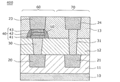
- FIG. 7 is a sectional view showing an example of a schematic configuration of a conventional nonvolatile memory device 400 described in Patent Document 2.
- the non-volatile storage device 400 disclosed in FIG. 7 is included in the first interlayer insulating layer 11, the second interlayer insulating layer 12, and the third interlayer insulating layer 13 of the storage area 60 and the circuit area 70 arranged on the substrate 10. , And is configured by forming the components described below.
- the resistance change element 40 is formed in the storage region 60.
- the resistance change element 40 is formed between the first lower layer metal wiring 20 and the first upper layer metal wiring 23, and the lower electrode 41 and the resistance change layer 42 are formed. And an upper electrode 43. Further, a side wall protective layer 50 is formed on the side surface of the resistance changing element 40. Further, the lower electrode 41 of the resistance changing element 40 is connected to the first lower layer metal wiring 20 via the lower plug 30, and the upper electrode 43 is directly connected to the first upper layer metal wiring 23.
- the second lower layer metal wiring 21 and the second upper layer metal wiring 24 connected to the second lower layer metal wiring 21 via the first via 31 are formed.
- the thickness of the resistance changing element or the lower plug is reduced in response to miniaturization, the operating characteristics of the non-volatile storage device will be greatly affected.
- the present disclosure has been made in view of the above problems, and a nonvolatile memory device including a resistance change element between metal wiring layers of a fine LSI without affecting the operation characteristics of the nonvolatile memory device, and the same.
- a manufacturing method is provided.
- Non-volatile memory device of the present disclosure is a non-volatile memory device including a memory area formed on a substrate and a circuit area around the memory area, and a first lower layer metal wiring in the memory area.
- a lower plug connected to the first lower layer metal wiring, a resistance change element connected to the lower plug, and a first upper layer metal wiring electrically connected to the resistance change element are formed in this order from below.
- Vias and second upper-layer metal wirings connected to the second vias are formed in this order from below, and the first lower-layer metal wirings and the second lower-layer metal wirings are metal wirings formed in the same layer. And the first upper-layer metal wiring and the second upper-layer metal wiring are metal wirings formed in the same layer, and at least one of upper surfaces and lower surfaces of the variable resistance element and the middle-layer metal wiring. They are located at different heights with respect to the surface of the substrate.
- one aspect of a method for manufacturing a nonvolatile memory device is a method for manufacturing a nonvolatile memory device including a memory area formed on a substrate and a circuit area around the memory area, wherein A first lower-layer metal wiring, a lower plug connected to the first lower-layer metal wiring, a resistance change element connected to the lower plug, and a first upper-layer metal wiring electrically connected to the resistance change element, From the second lower layer metal wiring, the first via connected to the second lower layer metal wiring, the middle layer metal wiring connected to the first via, and the middle layer metal wiring in the circuit region.
- a step of forming a second via to be connected and a second upper layer metal wiring to be connected to the second via in this order from below is provided, and the first lower layer metal wiring and the second lower layer metal wiring are formed in the same layer.
- the first upper-layer metal wiring and the second upper-layer metal wiring are formed in the same layer, and the upper surface of the resistance change element and the upper surface of the middle-layer metal wiring are located at positions different in height from the substrate surface. There is, or the lower surface of the resistance changing element and the lower surface of the middle layer metal wiring are at different heights with respect to the substrate surface, or the upper surface of the resistance changing element and the upper surface of the middle layer metal wiring. Are at different heights with respect to the substrate surface, and the lower surface of the resistance changing element and the lower surface of the middle layer metal wiring are at different heights with respect to the substrate surface.
- nonvolatile memory device including a resistance change element between metal wiring layers of a fine LSI and a manufacturing method thereof without affecting the operation characteristics of the nonvolatile memory device.
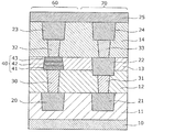
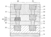
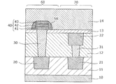
- FIG. 1 is a cross-sectional view showing an example of a schematic configuration of the nonvolatile memory device according to the first embodiment.
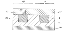
- FIG. 2A is a cross-sectional view showing the method for manufacturing the nonvolatile memory device according to the example of the first embodiment.
- FIG. 2B is a cross-sectional view showing the method for manufacturing the nonvolatile memory device according to the example of the first embodiment.
- FIG. 2C is a cross-sectional view showing the method for manufacturing the nonvolatile memory device according to the example of the first embodiment.
- FIG. 2D is a cross-sectional view showing the method for manufacturing the nonvolatile memory device according to the example of the first embodiment.
- FIG. 2A is a cross-sectional view showing the method for manufacturing the nonvolatile memory device according to the example of the first embodiment.
- FIG. 2B is a cross-sectional view showing the method for manufacturing the nonvolatile memory device according to the example of the first embodiment.
- FIG. 2C is a cross-
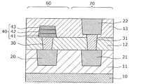
- FIG. 2E is a cross-sectional view showing the method for manufacturing the nonvolatile memory device according to the example of the first embodiment.
- FIG. 2F is a cross-sectional view showing the method for manufacturing the nonvolatile memory device according to the example of the first embodiment.
- FIG. 2G is a cross-sectional view showing the method for manufacturing the nonvolatile memory device according to the example of the first embodiment.
- FIG. 2H is a cross-sectional view showing the method for manufacturing the nonvolatile memory device according to the example of the first embodiment.
- 2I is a cross-sectional view showing the method for manufacturing the nonvolatile memory device according to the example of the first embodiment.
- FIG. 2J is a cross-sectional view showing the method for manufacturing the nonvolatile memory device according to the example of the first embodiment.
- FIG. 2K is a cross-sectional view showing the method for manufacturing the nonvolatile memory device according to the example of the first embodiment.
- FIG. 2L is a cross-sectional view showing the method for manufacturing the nonvolatile memory device according to the example of the first embodiment.
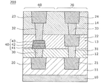
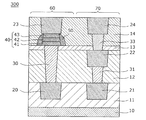
- FIG. 3 is a cross-sectional view showing an example of a schematic configuration of the nonvolatile memory device according to the second embodiment.
- FIG. 4A is a cross-sectional view showing the method for manufacturing the nonvolatile memory device according to the example of the second embodiment.
- FIG. 4B is a cross-sectional view showing the method for manufacturing the nonvolatile memory device according to the example of the second embodiment.
- FIG. 4C is a cross-sectional view showing the method for manufacturing the nonvolatile memory device according to the example of the second embodiment.
- FIG. 4D is a cross-sectional view showing the method for manufacturing the nonvolatile memory device according to the example of the second embodiment.
- FIG. 4E is a cross-sectional view showing the method for manufacturing the nonvolatile memory device according to the example of the second embodiment.
- FIG. 4F is a cross-sectional view showing the method for manufacturing the nonvolatile memory device according to the example of the second embodiment.
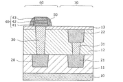
- FIG. 5 is a sectional view showing an example of the schematic configuration of the nonvolatile memory device according to the third embodiment.
- FIG. 6A is a cross-sectional view showing the method for manufacturing the nonvolatile memory device according to the example of the third embodiment.
- FIG. 6B is a cross-sectional view showing the method for manufacturing the nonvolatile memory device according to the example of the third embodiment.
- FIG. 6C is a cross-sectional view showing the method for manufacturing the nonvolatile memory device according to the example of the third embodiment.
- FIG. 6D is a cross-sectional view showing the method for manufacturing the nonvolatile memory device according to the example of the third embodiment.
- FIG. 6E is a cross-sectional view showing the method for manufacturing the nonvolatile memory device according to the example of the third embodiment.
- FIG. 6F is a cross-sectional view showing the method for manufacturing the nonvolatile memory device according to the example of the third embodiment.
- FIG. 6G is a cross-sectional view showing the method for manufacturing the nonvolatile memory device according to the example of the third embodiment.
- FIG. 6H is a cross-sectional view showing the method for manufacturing the nonvolatile memory device according to the example of the third embodiment.
- FIG. 7 is a cross-sectional view showing an example of a schematic configuration of a conventional non-volatile storage device.
- the “oxygen deficiency” shown in the embodiment of the present disclosure means that each metal oxide has a stoichiometric composition (when a plurality of stoichiometric compositions are present, the most of them). It refers to the ratio of oxygen deficient to the amount of oxygen that constitutes the oxide having a high resistance stoichiometric composition. In other words, metal oxides of stoichiometric composition are more stable and have higher resistance values than metal oxides of other compositions.
- the metal is tantalum (Ta)
- the stoichiometric oxide composition according to the above definition is Ta 2 O 5 , and thus can be expressed as TaO 2.5 .
- the oxygen deficiency of TaO 2.5 is 0%.
- the oxygen excess metal oxide has a negative oxygen deficiency.
- the oxygen deficiency is described as including both a positive value, 0, and a negative value.
- an oxide having a small oxygen deficiency has a high resistance value because it is closer to an oxide having a stoichiometric composition, and an oxide having a large oxygen deficiency has a low resistance value because it is closer to a metal constituting the oxide. become. That is, the metal oxide becomes conductive by making it an oxygen-deficient type.
- the “oxygen content” shown in the embodiments of the present disclosure is represented by the ratio of the number of oxygen atoms contained to the total number of atoms forming the metal oxide.
- the oxygen content of Ta 2 O 5 is the ratio of the number of oxygen atoms to the total number of atoms (O/(Ta+O)), which is 71.4 atm %. Therefore, the oxygen-deficient tantalum oxide has an oxygen content of more than 0 and less than 71.4 atm%.
- the oxygen content corresponds to the degree of oxygen deficiency. That is, when the oxygen content of the second metal oxide is larger than the oxygen content of the first metal oxide, the oxygen deficiency of the second metal oxide is smaller than the oxygen deficiency of the first metal oxide.
- the relationship between the oxygen deficiency and the oxygen content can be paraphrased.
- the oxygen content of the first metal oxide is smaller than the oxygen content of the second metal oxide.
- the “insulator” shown in the embodiment of the present disclosure follows a general definition. That is, a material having a resistivity of 10 8 ⁇ cm or more is shown (Non-Patent Document: “Semiconductor Engineering for Integrated Circuits” Industrial Research Group (1992) Akira Usami, Shinji Kanebo, Takao Maekawa, Tomokei Hajime, Morio Inoue). In contrast, “conductor” indicates that resistivity is composed of less than 10 8 [Omega] cm material.
- the resistivity of the first metal oxide differs from that of the second metal oxide by 4 digits to 6 digits or more. Further, the resistivity of the variable resistance element after the execution of the initial breakdown operation, for example, 10 4 [Omega] cm approximately.
- the "standard electrode potential" is generally an index of susceptibility to oxidation, and a large value means less oxidization, and a smaller value means oxidization.
- the nonvolatile memory device it is necessary to make the thickness of the insulating film between the wiring layers of the lower layer metal wiring and the upper layer metal wiring thinner than the thickness of the conventional variable resistance element plus the thickness of the lower plug. The sex is coming out. In order to meet this requirement, for example, in the case of the conventional non-volatile storage device 400 shown in FIG. 7, it is necessary to reduce the thickness of the resistance changing element itself and the thickness of the lower plug.
- variable resistance element is directly formed on the lower layer metal wiring by omitting the lower plug
- a process damage such as corrosion of the lower layer metal wiring may occur in a dry etching process when patterning the variable resistance element. The problem of giving it occurs.
- the non-volatile storage device and the manufacturing method thereof according to one aspect of the present disclosure have the following features.
- Non-volatile memory device of the present disclosure is a non-volatile memory device including a memory area formed on a substrate and a circuit area around the memory area, and a first lower layer metal wiring in the memory area.
- a lower plug connected to the first lower layer metal wiring, a resistance change element connected to the lower plug, and a first upper layer metal wiring electrically connected to the resistance change element are formed in this order from below.
- Vias and second upper-layer metal wirings connected to the second vias are formed in this order from below, and the first lower-layer metal wirings and the second lower-layer metal wirings are metal wirings formed in the same layer. And the first upper-layer metal wiring and the second upper-layer metal wiring are metal wirings formed in the same layer, and at least one of upper surfaces and lower surfaces of the variable resistance element and the middle-layer metal wiring. They are located at different heights with respect to the surface of the substrate.
- the resistance change element and the middle-layer metal wiring are formed in the same interlayer insulating film, and the upper surface of the resistance change element and the upper surface of the middle-layer metal wiring are May be coplanar.
- the resistance change element and the middle-layer metal wiring are formed in the same interlayer insulating film, and the upper surface of the resistance change element and the upper surface of the middle-layer metal wiring are Need not be coplanar.
- the upper surface of the resistance changing element may be located lower than the upper surface of the middle layer metal wiring with respect to the substrate surface.
- the lower surface of the resistance changing element may be located higher than the upper surface of the middle layer metal wiring with respect to the substrate surface.
- the upper surface of the resistance changing element may be located higher than the upper surface of the middle layer metal wiring with respect to the substrate surface.
- the upper surface of the resistance changing element may be in direct contact with the first upper layer metal wiring.
- one aspect of a method for manufacturing a nonvolatile memory device is a method for manufacturing a nonvolatile memory device including a memory area formed on a substrate and a circuit area around the memory area, wherein A first lower-layer metal wiring, a lower plug connected to the first lower-layer metal wiring, a resistance change element connected to the lower plug, and a first upper-layer metal wiring electrically connected to the resistance change element, From the second lower layer metal wiring, the first via connected to the second lower layer metal wiring, the middle layer metal wiring connected to the first via, and the middle layer metal wiring in the circuit region.
- a step of forming a second via to be connected and a second upper layer metal wiring to be connected to the second via in this order from below is provided, and the first lower layer metal wiring and the second lower layer metal wiring are formed in the same layer.
- the first upper-layer metal wiring and the second upper-layer metal wiring are formed in the same layer, and the upper surface of the resistance change element and the upper surface of the middle-layer metal wiring are located at positions different in height from the substrate surface.
- the lower surface of the variable resistance element and the lower surface of the middle-layer metal wiring are at different heights with respect to the surface of the substrate, or the upper surface of the variable resistance element and the upper surface of the middle-layer metal wiring.
- the lower surface of the resistance changing element and the lower surface of the middle layer metal wiring are at different heights with respect to the substrate surface.
- one aspect of the method of manufacturing the non-volatile storage device of the present disclosure is a step of forming a first interlayer insulating layer on the substrate and a first lower layer metal wiring in the storage area of the first interlayer insulating layer. At the same time as forming, forming a second lower layer metal wiring in the circuit region of the first interlayer insulating layer, and on the first interlayer insulating layer including the first lower layer metal wiring and the second lower layer metal wiring.
- Forming a second interlayer insulating layer, forming a lower plug connected to the first lower layer metal wiring in the storage region of the second interlayer insulating layer, and the second interlayer insulating including the lower plug A step of forming a resistance changing element connected to the lower plug in the storage area on the layer, a step of forming a third interlayer insulating layer on the second interlayer insulating layer including the resistance changing element, and the first step. Forming a first via connected to the second lower metal wiring and an intermediate metal wiring connected to the first via in the circuit region of the second interlayer insulating layer and the third interlayer insulating layer; and the variable resistance element.
- a second via connecting to the middle layer metal wiring and a second upper layer metal wiring connecting to the second via are formed in the circuit region of the fourth interlayer insulating layer.
- the upper surface of the variable resistance element and the upper surface of the middle-layer metal wiring are in the same plane, and the thickness of the variable resistance element may be different from the thickness of the middle-layer metal wiring.
- another aspect of the method for manufacturing the non-volatile storage device of the present disclosure is a step of forming a first interlayer insulating layer on the substrate and a first lower layer metal in the storage region of the first interlayer insulating layer. Forming a wiring and simultaneously forming a second lower layer metal wiring in the circuit region of the first interlayer insulating layer; and the first interlayer insulating layer including the first lower layer metal wiring and the second lower layer metal wiring. Forming a second interlayer insulating layer thereon; forming a lower plug connected to the first lower metal wiring in the storage region of the second interlayer insulating layer; and the second plug including the lower plug.
- a second via and a second via which form an upper plug connected to the device and a first upper layer metal wiring connected to the upper plug, and simultaneously connect to the middle layer metal wiring in the circuit region of the fourth interlayer insulating layer.
- the upper surface of the resistance changing element may be located lower than the upper surface of the middle layer metal wiring with respect to the surface of the substrate, which comprises a step of forming a second upper layer metal wiring connected to the above.
- another aspect of the method for manufacturing the non-volatile storage device of the present disclosure is a step of forming a first interlayer insulating layer on the substrate and a first lower layer metal in the storage region of the first interlayer insulating layer. Forming a wiring and simultaneously forming a second lower layer metal wiring in the circuit region of the first interlayer insulating layer; and the first interlayer insulating layer including the first lower layer metal wiring and the second lower layer metal wiring. Forming a second interlayer insulating layer thereon, and forming a first via connecting to the second lower layer metal wiring and a middle-layer metal wiring connecting to the first via in the circuit region of the second interlayer insulating layer.
- a second via connecting to the middle metal wiring and a second upper layer metal wiring connecting to the second via are formed in the circuit regions of the third interlayer insulating layer and the fourth interlayer insulating layer.
- the lower surface of the resistance changing element may be located higher than the upper surface of the middle layer metal wiring with respect to the surface of the substrate, which comprises a step of forming.
- a nonvolatile memory device having a resistance change element between metal wiring layers, which is compatible with a mass-production process of a fine LSI, and a process for forming a metal wiring by a step of forming the resistance change element. You can suppress damage.
- FIG. 1 is a cross-sectional view showing an example of a schematic configuration of the nonvolatile memory device 100 according to the first embodiment.
- the storage area 60 is provided with a large number of resistance changing elements 40, but for simplification of the drawings, only one of the large number of resistance changing elements 40 is shown in the following drawings. In addition, a part of the configuration is shown enlarged for easy understanding. Similarly, only one of a large number of wiring and via connection structures provided in the circuit area 70 adjacent to the storage area 60 is shown.
- the nonvolatile memory device 100 is characterized in that the upper surface of the resistance change element 40 is formed at the same height as the upper surface of the middle-layer metal wiring 22.
- the nonvolatile memory device 100 includes a memory region 60 and a circuit region 70, and includes a substrate 10, a first interlayer insulating layer 11 formed on the substrate 10, and a first memory region 60.
- First lower-layer metal wiring 20 formed in interlayer insulating layer 11, second lower-layer metal wiring 21 formed in first interlayer insulating layer 11 in circuit region 70, first lower-layer metal wiring 20 and second lower-layer
- a second interlayer insulating layer 12 formed on the first interlayer insulating layer 11 including the metal wiring 21, a lower plug 30 formed in the second interlayer insulating layer 12 and connected to the first lower layer metal wiring 20;
- a resistance changing element 40 formed on the two-layer insulating layer 12 and the lower plug 30 so as to be connected to the lower plug 30 and composed of a lower electrode 41, a resistance changing layer 42 and an upper electrode 43, and a second interlayer insulating layer.
- a third interlayer insulating layer 13 formed on 12 to cover the side surface portion of the resistance change element 40, and a first via 31 formed in the second interlayer insulating layer 12 and connected to the second lower metal wiring 21.
- the third interlayer including the middle-layer metal wiring 22 formed in the second interlayer insulation layer 12 and the third interlayer insulation layer 13 and connected to the first via 31, and the upper electrode 43 of the resistance change element 40 and the middle-layer metal wiring 22.
- the first upper metal wiring 23, the second via 33 formed in the fourth interlayer insulating layer 14 and connected to the middle metal wiring 22, and the second upper metal wiring 24 connected to the second via 33 are provided. ..
- the upper surface of the resistance change element 40 and the upper surface of the middle metal wiring 22 are formed at the same height with respect to the surface of the semiconductor substrate.
- the substrate 10 may be provided with active elements such as transistors electrically connected to the resistance change element 40.
- the storage area 60 may include a resistance changing element, a plug connected to the resistance changing element, wiring, and the like, as well as a selection transistor and the like in the 1T1R type storage device.
- the circuit area 70 may include a bit line decoder, a word line decoder, a power supply circuit, and the like, in addition to wirings and vias.
- the surface (upper surface) of the first lower layer metal wiring 20 and the second lower layer metal wiring 21 is flat, and is formed so as to be substantially flush with the surface of the first interlayer insulating layer 11.
- variable resistance element 40 can be, for example, a non-volatile memory element whose resistance value is reversibly changed by application of an electric pulse.
- the resistance changing element 40 may be, for example, a ReRAM (Resistive Random Access Memory).
- the resistance change element 40 includes a PRAM (Phase-change Random Access Memory) that uses phase change recording, an MRAM (Magnetoresistive Random Access Memory) that uses a magnetoresistive effect, and a FeRAM (RRAMFroFerc) that uses a ferroelectric. Access Memory) or the like may be used.
- the lower electrode 41 may be made of, for example, tantalum nitride having a thickness of 10 to 30 nm, but may also be made of tungsten, nickel, tantalum, titanium, aluminum, titanium nitride or the like.
- a transition metal oxide may be used as the metal oxide of the resistance change layer 42.
- a material that exhibits a standard electrode potential equal to or lower than that of tantalum and is unlikely to change in resistance may be used for the lower electrode 41.
- At least one material selected from the group consisting of tantalum, tantalum nitride, titanium, titanium nitride, and titanium-aluminum nitride can be used for the lower electrode 41. With a structure made of such a material, stable memory characteristics can be realized.
- the lower electrode 41 may be physically connected to the lower plug 30 or may be connected to the lower plug 30 via a conductor. In the example shown in FIG. 1, the lower electrode 41 is physically connected to the lower plug 30.
- the resistance change layer 42 is provided between the lower electrode 41 and the upper electrode 43, and based on an electrical signal provided between the lower electrode 41 and the upper electrode 43, the high resistance state and the high resistance state It reversibly changes between a low resistance state and a low resistance state.
- the resistance change layer 42 is sandwiched between the lower electrode 41 and the upper electrode 43, and is composed of a layer made of oxygen-deficient tantalum oxide having a thickness of 5 nm or more and 50 nm or less.
- the resistance changing layer 42 may also be made of titanium oxide, nickel oxide, hafnium oxide, zirconium oxide, niobium oxide, tungsten oxide, aluminum oxide or the like.
- the resistance change layer 42 may be a single layer or may be composed of a plurality of layers having different oxygen contents. When it is composed of a plurality of layers, a first resistance change layer composed of a first metal oxide and a second resistance change layer composed of a second metal oxide having an oxygen content higher than that of the first metal oxide. At least two layers including and may be provided.
- the resistance change layer 42 may have a laminated structure including two layers, a first resistance change layer and a second resistance change layer.
- the first resistance change layer may be made of oxygen-deficient tantalum oxide (TaO x , 0 ⁇ x ⁇ 2.5).
- the second resistance change layer may be made of tantalum oxide (TaO y , x ⁇ y) having a lower oxygen deficiency than the first resistance change layer.
- first metal forming the first metal oxide and the second metal forming the second metal oxide are tantalum
- present invention is not limited to this and other
- the metal may form the first metal oxide and the second metal oxide.
- first metal oxide and the second metal oxide may be composed of metal oxides of different metals.
- first metal oxide and the second metal oxide constituting the resistance changing layer 42 may contain at least one selected from the group consisting of the transition metal oxide and the aluminum oxide, respectively.
- each of the first metal oxide and the second metal oxide forming the resistance change layer 42 includes at least one selected from the group consisting of tantalum oxide, hafnium oxide, and zirconium oxide. You may stay.
- first metal and the second metal in addition to tantalum, for example, at least one selected from the group consisting of titanium (Ti), hafnium (Hf), zirconium (Zr), niobium (Nb), and tungsten (W).
- Ti titanium
- Hf hafnium
- Zr zirconium
- Nb niobium
- W tungsten
- Two transition metals may be used. Since the transition metal can have a plurality of oxidation states, different resistance states can be realized by a redox reaction. Further, aluminum (Al) may be used as the first metal and the second metal.
- the composition of the first metal oxide forming the first resistance change layer is HfO x
- the composition of the second metal oxide forming the second resistance change layer is HfO y
- x ⁇ y may be satisfied.
- x and y may be 0.9 ⁇ x ⁇ 1.6 and 1.8 ⁇ y ⁇ 2.0 may be satisfied.
- the high oxygen deficiency layer (first resistance change layer) using hafnium oxide can be generated by, for example, a reactive sputtering method in which an Hf target is used and sputtering is performed in argon gas and oxygen gas.
- the oxygen content of the high oxygen deficiency layer can be easily adjusted by changing the flow rate ratio of the oxygen gas to the argon gas during the reactive sputtering, as in the case of the tantalum oxide described above. It is not essential to heat the substrate, and the substrate temperature may be room temperature.
- the low oxygen deficiency layer (second resistance change layer) using hafnium oxide can be formed, for example, by exposing the surface of the high oxygen deficiency layer to plasma of a mixed gas of argon gas and oxygen gas.
- the thickness of the low oxygen deficiency layer can be easily adjusted by the exposure time of the mixed gas of argon gas and oxygen gas to the plasma.
- the thickness of the second resistance change layer may be 3 to 4 nm.
- x When zirconium oxide is used, when the composition of the first metal oxide forming the first resistance change layer is ZrO x and the composition of the second metal oxide forming the second resistance change layer is ZrO y , x The relationship of ⁇ y may be satisfied. Further, x and y are 0.9 ⁇ x ⁇ 1.4, and 1.9 ⁇ y ⁇ 2.0 may be satisfied.
- the high oxygen deficiency layer (first resistance change layer) using zirconium oxide can be formed by, for example, a reactive sputtering method in which a Zr target is used and sputtering is performed in argon gas and oxygen gas.
- the oxygen content of the high oxygen deficiency layer can be easily adjusted by changing the flow rate ratio of the oxygen gas to the argon gas during the reactive sputtering, as in the case of the tantalum oxide described above.
- the substrate temperature can be room temperature without any particular heating.
- the low oxygen deficiency layer (second resistance change layer) using zirconium oxide can be formed, for example, by exposing the surface layer portion of the high oxygen deficiency layer to plasma of a mixed gas of argon gas and oxygen gas. ..
- the thickness of the low oxygen deficiency layer can be easily adjusted by the exposure time of the mixed gas of argon gas and oxygen gas to the plasma.
- the thickness of the second resistance change layer may be 1 to 5 nm.
- the hafnium oxide layer and the zirconium oxide layer described above can also be formed by using a CVD (Chemical Vapor Deposition) method or an ALD (Atomic Layer Deposition) method instead of the sputtering method.
- CVD Chemical Vapor Deposition
- ALD Atomic Layer Deposition
- the second metal oxide a material having a smaller oxygen deficiency degree (higher resistance value) than that of the first metal oxide may be selected.
- the voltage applied between the lower electrode and the upper electrode is more distributed to the second resistance changing layer.
- oxygen that can contribute to the reaction is also abundant. Therefore, a redox reaction occurs selectively at the interface between the upper electrode and the second variable resistance layer, and stable resistance change can be realized. As a result, the redox reaction can be more likely to occur in the second resistance changing layer.
- different metals may be used for the first metal constituting the first metal oxide and the second metal constituting the second metal oxide. Since the resistance change phenomenon in the resistance change layer containing the oxygen-deficient metal oxide is manifested by the movement of oxygen, it is sufficient that at least oxygen movement is possible even if the type of the parent metal is different. Therefore, even if different metals are used for the first metal forming the first variable resistance layer and the second metal forming the second variable resistance layer, it is considered that the same effect is achieved.
- the standard electrode potential of the second metal may be lower than the standard electrode potential of the first metal.
- the resistance change phenomenon occurs when a redox reaction occurs in a minute filament (conductive path) formed in the second metal oxide forming the second resistance change layer having a high resistance, and the resistance value changes. This is because it is considered.
- oxygen-deficient tantalum oxide (TaO x ) may be used for the first variable resistance layer
- aluminum oxide Al 2 O 3 ) may be used for the second variable resistance layer.
- the high oxygen deficiency layer and the low oxygen deficiency layer may include an oxide layer such as tantalum, hafnium, zirconium, or an aluminum oxide layer as the main resistance change layer that exhibits resistance change. Besides, for example, a trace amount of another element may be contained.
- the resistance change layer is formed by using the sputtering method
- unintended trace elements may be mixed in the resistance change layer due to residual gas or gas release from the wall of the vacuum container.
- it is also included in the scope of the present disclosure.
- the resistance change layer 42 does not necessarily have to be composed of two layers, and may be composed of three or more layers, or conversely, may be composed of one layer.
- the upper electrode 43 is an electrode formed above the lower electrode 41.
- the upper electrode 43 is formed on the resistance change layer 42.
- the upper electrode 43 may be made of a noble metal material such as iridium, platinum, or palladium having a thickness of 5 nm or more and 50 nm or less.
- the upper electrode 43 is made of, for example, at least one material selected from the group consisting of iridium, platinum (Pt), and palladium (Pd), and the metal constituting the resistance change layer 42 and the lower electrode 41 are compared with the upper electrode material. It may be made of a material having a higher standard electrode potential. With such a configuration, a redox reaction is selectively generated in the vicinity of the interface between the upper electrode 43 and the resistance change layer 42 in the resistance change layer 42, and a stable resistance change phenomenon is realized.
- the upper electrode 43 of the storage area 60 and the middle layer metal wiring 22 of the circuit area 70 have flat surfaces (upper surfaces) and are flush with the surface of the third interlayer insulating layer 13. It is formed.
- the first lower-layer metal wiring 20, the second lower-layer metal wiring 21, the middle-layer metal wiring 22, the first upper-layer metal wiring 23, and the second upper-layer metal wiring 24 all have the same thickness, and the first via 31, the upper plug 32, and the The two vias 33 may all have the same thickness (height).
- FIGS. 2A to 2L are cross-sectional views showing a method of manufacturing the non-volatile storage device 100 according to the first embodiment.
- the method for manufacturing the nonvolatile memory device according to the present embodiment will be described with reference to FIGS. 2A to 2L.
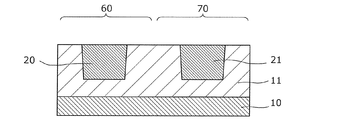
- FIG. 2A is a diagram showing a process of forming the first lower layer metal wiring 20 in the first interlayer insulating layer 11 of the memory area 60 and the second lower layer metal wiring 21 in the first interlayer insulating layer 11 of the circuit area 70. is there.
- the first interlayer insulating layer 11 is formed on a substrate 10 made of a semiconductor on which an active element or the like (not shown) is formed in advance, and the first lower layer metal wiring 20 and the second lower layer metal wiring are formed by the damascene method. 21 is formed by embedding.
- the first interlayer insulating layer 11 made of silicon oxide, silicon nitride, silicon oxynitride, silicon oxycarbide, silicon carbonitride, or the like is formed on the substrate 10 by using plasma CVD or the like. To do.
- a wiring groove for embedding the first lower layer metal wiring 20 and the second lower layer metal wiring 21 in the first interlayer insulating layer 11 is formed by photolithography and dry etching.
- a barrier metal layer composed of tantalum nitride (5 nm or more and 40 nm or less) and tantalum (5 nm or more and 40 nm or less) and a wiring material of copper (50 nm or more and 300 nm or less) are formed in the formed wiring groove by a sputtering method or the like. To be deposited. Then, by further depositing copper using copper as a seed by an electrolytic plating method or the like, all the wiring grooves are filled with copper as a wiring material and a barrier metal layer.
- First lower-layer metal wiring 20 and second lower-layer metal wiring 21 are formed so as to be flush with the surface (upper surface).
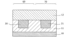
- FIG. 2B is a diagram showing a step of forming the second interlayer insulating layer 12 so as to cover the first interlayer insulating layer 11.
- silicon oxide, silicon nitride, silicon oxynitride, etc. are used on the first interlayer insulating layer 11 on which the first lower layer metal wiring 20 and the second lower layer metal wiring 21 are formed by using plasma CVD or the like.
- a second interlayer insulating layer 12 made of silicon oxycarbide, silicon carbonitride, or the like is formed.
- the thickness of the second interlayer insulating layer 12 may be, for example, 30 nm or more and 200 nm or less.
- FIG. 2C is a diagram showing a process of forming the lower plug 30.
- the lower plug 30 connected to the first lower layer metal wiring 20 is formed in the second interlayer insulating layer 12.
- a plug hole for burying and forming a lower plug 30 connected to the first lower layer metal wiring 20 is formed in the second interlayer insulating layer 12.
- a barrier metal layer composed of tantalum nitride (thickness: 5 nm or more and 40 nm or less) and tantalum (thickness: 5 nm or more and 40 nm or less) is formed on the second interlayer insulating layer 12 including the formed plug hole, and a plug.
- Copper thickness: 50 nm or more and 300 nm or less
- copper is further deposited by an electrolytic plating method or the like to fill all the plug holes with the barrier metal layer and copper.
- tungsten or the like can be adopted in addition to copper.
- the excess copper and the excess barrier metal layer on the second interlayer insulating layer 12 and the surface of the plug hole are removed by the CMP method to form a flat surface and the surface (upper surface) of the second interlayer insulating layer 12.
- a lower plug 30 having the same plane is formed.
- FIG. 2D is a diagram showing a process of forming a resistance changing element 40 connected to the lower plug 30 on the second interlayer insulating layer 12.
- the lower electrode material layer, the resistance change material layer, and the upper electrode material layer are formed in this order on the second interlayer insulating layer 12 including the lower plug 30.
- a lower electrode material layer made of tantalum nitride, a resistance change material layer (thickness: 20 nm), and iridium.
- an upper electrode material layer (thickness: 40 nm) are sequentially deposited by a sputtering method or the like.
- the resistance-changing material layer is deposited by a reactive sputtering method in which metal tantalum is used as a target and sputtering is performed in an oxygen-containing argon atmosphere.
- a resist mask for patterning the resistance changing element 40 is formed on the upper electrode material layer using photolithography.
- the upper electrode material layer, the resistance changing material layer and the lower electrode material layer are sequentially patterned using the resist mask by a dry etching method, and then the resist mask is removed by an ashing treatment. As a result, the resistance change element 40 is formed.
- the resistance changing element 40 is formed from the surface of the first lower layer metal wiring 20 to the lower plug 30. They can be arranged separated by a height (corresponding to the thickness of the second interlayer insulating layer 12). Therefore, it is possible to prevent the surface of the first lower layer metal wiring 20 from being corroded or altered by chlorine gas or fluorine gas used during dry etching when patterning and forming the resistance changing element 40, oxygen gas used during ashing, or the like.
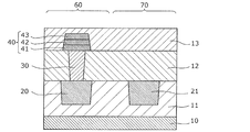
- FIG. 2E is a diagram showing a step of forming the third interlayer insulating layer 13 so as to cover the resistance change element 40.
- the resistance changing element 40 and the second interlayer insulating layer 12 are composed of silicon oxide, silicon nitride, silicon oxynitride, silicon acid carbide, silicon carbonitride, or the like by using plasma CVD or the like.
- the third interlayer insulating layer 13 is formed.
- the thickness of the third interlayer insulating layer 13 may be 100 nm or more and 500 nm or less.
- the storage area 60 in which the resistance changing element 40 is formed and the circuit area 70 in which the resistance changing element is not formed are formed in the third interlayer insulating layer 13.
- the height of the top surface is different. Therefore, using the CMP method, the heights of the upper surfaces of the third interlayer insulating layer 13 of the storage area 60 and the circuit area 70 are made uniform and flattened.
- the thickness of the third interlayer insulating layer 13 on the resistance change element 40 after CMP may be 10 nm or more and 100 nm or less.
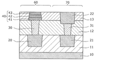
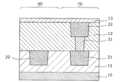
- 2F to 2H are diagrams showing a process of forming the first via 31 and the middle-layer metal wiring 22.
- the third interlayer insulating layer 13 and the second interlayer insulating layer 12 in the circuit region 70 are connected to the second lower metal wiring 21.
- a first via hole 31a for embedding the first via 31 is formed.
- a wiring groove 22a for embedding and forming the middle layer metal wiring 22 is formed in the third interlayer insulating layer 13 and the second interlayer insulating layer 12 so as to be connected to the first via hole 31a.
- the first via hole 31a is formed by photolithography and dry etching. Further, the wiring groove 22a is formed again by using photolithography and dry etching.
- the first via hole 31a for the first via 31 is formed first by the first photolithography and dry etching, and the wiring for the middle layer metal wiring 22 is formed by the second photolithography and dry etching.
- the groove 22a is formed, the first via hole 31a may be formed after the wiring groove 22a is formed first.
- tantalum nitride (thickness: 5 nm or more and 40 nm or less) and tantalum (thickness:: 5 nm or more and 40 nm or less) are formed in the first via hole 31a and the wiring groove 22a.
- a barrier metal layer composed of 5 nm or more and 40 nm or less) and a wiring material copper (thickness: 50 nm or more and 300 nm or less) are deposited by using a sputtering method or the like.
- the wiring material and the barrier metal layer 25 are formed by further depositing copper by electrolytic plating or the like, and the first via hole 31a and the wiring groove 22a are all filled with the wiring material copper and the barrier metal layer.
- the excess copper and the excess barrier metal layer on the surface of the copper deposited by the CMP method are removed, and the surface (upper surface) of the upper electrode 43 of the resistance changing element 40 is further overpolished.
- the surface of the third interlayer insulating layer 13 and the middle metal wiring 22 is CMP-polished, and the surface of the third interlayer insulating layer 13 and the surface of the upper electrode 43 and the surface of the middle metal wiring 22 are flush with each other. Finish as if to be eggplant.
- FIG. 2I is a diagram showing a step of forming the fourth interlayer insulating layer 14 on the third interlayer insulating layer 13.
- a silicon oxide, a silicon nitride, a silicon nitride, a silicon oxycarbide, or a silicon oxycarbide is used by using plasma CVD or the like.
- a fourth interlayer insulating layer 14 made of silicon carbonitride or the like is formed. The thickness of the fourth interlayer insulating layer 14 may be 100 nm or more and 300 nm or less.
- 2J to 2L are diagrams showing a process of forming the upper plug 32, the second via 33, the first upper layer metal wiring 23, and the second upper layer metal wiring 24.
- the upper plug 32 connected to the upper electrode 43 of the resistance changing element 40 is embedded and formed in the fourth interlayer insulating layer 14 of the storage area 60.
- Upper plug hole 32a is formed.
- a second via hole 33a for embedding and forming a second via 33 connected to the middle layer metal wiring 22 is formed in the fourth interlayer insulating layer 14 of the circuit region 70.
- a wiring groove 23a for embedding the first upper layer metal wiring 23 and a second via hole 33a are formed so as to be connected to the upper plug hole 32a.
- a wiring groove 24a for embedding the upper metal wiring 24 is formed.
- the upper plug hole 32a and the second via hole 33a are simultaneously formed by photolithography and dry etching. Further, again, the wiring grooves 23a and 24a are simultaneously formed by using photolithography and dry etching.
- the upper plug hole 32a and the second via hole 33a are formed by the first photolithography and dry etching, and the wiring grooves 23a and 24a are formed by the second photolithography and dry etching.
- the wiring grooves 23a and 24a may be formed first.
- a barrier metal layer composed of an object (thickness: 5 nm or more and 40 nm or less) and tantalum (thickness: 5 nm or more and 40 nm or less) and copper (thickness: 50 nm or more and 300 nm or less) as a wiring material are deposited by a sputtering method or the like.
- the wiring material and the barrier metal layer 25 are formed by further depositing copper by an electrolytic plating method or the like, and the upper plug hole 32a and the second via hole 33a and the wiring grooves 23a and 24a are all made of the wiring material copper and the barrier metal. Fill with layers.
- a non-volatile storage device having an affinity with the mass production process of existing fine LSIs and having a resistance changing element between metal wiring layers is realized. it can.
- FIG. 3 is a cross-sectional view showing an example of a schematic configuration of the nonvolatile memory device 200 according to the second embodiment.
- FIGS. 3 and 4A to 4F are cross-sectional views showing a method for manufacturing the nonvolatile memory device 200 according to the second embodiment.
- the nonvolatile memory device according to the present embodiment and the manufacturing method thereof will be described with reference to FIGS. 3 and 4A to 4F.
- the non-volatile storage device 200 is characterized in that the upper surface of the resistance changing element 40 is formed at a position lower than the upper surface of the middle layer metal wiring 22.
- FIG. 4A a first lower layer metal wiring 20 and a second lower layer metal wiring 21 are formed in a first interlayer insulating layer 11 on a substrate 10, and a first lower layer metal wiring 20 and a second lower layer metal wiring 21 are included.
- FIG. 6 is a diagram showing a step of forming a second interlayer insulating layer 12 on the interlayer insulating layer 11 and forming a lower plug 30 connected to the first lower layer metal wiring 20 in the second interlayer insulating layer 12 of the storage region 60. ..
- a plug hole for burying and forming a lower plug 30 connected to the first lower layer metal wiring 20 is formed in the second interlayer insulating layer 12.
- a barrier metal layer composed of tantalum nitride and tantalum and copper as a plug material are deposited on the second interlayer insulating layer 12 including the formed plug holes by a sputtering method or the like.
- copper is further deposited by an electrolytic plating method or the like to fill all the plug holes with the barrier metal layer and copper.
- the surface is flat and flush with the surface of the second interlayer insulating layer 12.
- the eggplant lower plug 30 is formed.
- FIG. 4B is a diagram showing a step of forming the resistance change element 40 connected to the lower plug 30 on the second interlayer insulating layer 12.
- the resistance changing element 40 is formed so as to be connected to the first lower layer metal wiring 20 via the lower plug 30, so that the resistance changing element 40 is formed on the surface of the first lower layer metal wiring 20.
- the height of the lower plug 30 (corresponding to the thickness of the second interlayer insulating layer 12). Therefore, it is possible to prevent the surface of the first lower layer metal wiring 20 from being corroded or altered by chlorine gas or fluorine gas used during dry etching when patterning and forming the resistance changing element 40, oxygen gas used during ashing, or the like.
- FIG. 4C is a diagram showing a step of forming the third interlayer insulating layer 13 so as to cover the resistance change element 40.
- a silicon oxide, a silicon nitride, a silicon oxynitride, a silicon acid carbide, a silicon carbonitride, or the like is formed by using plasma CVD or the like.
- a third interlayer insulating layer 13 is formed.
- the thickness of the third interlayer insulating layer 13 may be 100 nm or more and 500 nm or less.
- the third interlayer insulating layer 13 is formed in the memory region 60 where the resistance change element 40 is formed and the circuit region 70 where the resistance change element is not formed.
- the height of the upper surface is different. Therefore, the CMP method is used to flatten the upper surfaces of the third interlayer insulating layer 13 in the memory region 60 and the circuit region 70 so as to be uniform in height.
- the thickness of the third interlayer insulating layer 13 on the resistance change element 40 after CMP may be 10 nm or more and 100 nm or less.
- FIG. 4D is a diagram showing a step of forming the first via 31 and the middle-layer metal wiring 22.
- a first via 31 is formed in the third interlayer insulating layer 13 and the second interlayer insulating layer 12 of the circuit region 70 so as to be connected to the second lower metal wiring 21.
- the middle-layer metal wiring 22 is formed in the third interlayer insulating layer 13 so as to be connected to the first via 31.
- a via hole is formed by photolithography and dry etching. Further, the wiring groove is formed again by using photolithography and dry etching. Next, a barrier metal layer composed of tantalum nitride and tantalum and copper as a wiring material are deposited in the via hole and the wiring groove by using a sputtering method or the like. Then, the via hole and the wiring groove are all filled with the wiring material copper and the barrier metal layer by further depositing copper by an electrolytic plating method or the like.
- the via hole for the first via 31 is formed first by the first photolithography and dry etching, and the middle layer metal wiring 22 is formed by the second photolithography and dry etching.
- the wiring groove for forming is formed, the via hole may be formed after forming the wiring groove first.
- FIG. 4E is a diagram showing a step of forming the fourth interlayer insulating layer 14 on the third interlayer insulating layer 13.
- the third interlayer insulating layer 13 including the middle layer metal wiring 22 it is composed of silicon oxide, silicon nitride, silicon oxynitride, silicon acid carbide, silicon carbonitride, etc. by using plasma CVD or the like.
- a fourth interlayer insulating layer 14 is formed.
- the thickness of the fourth interlayer insulating layer 14 may be 100 nm or more and 300 nm or less.
- FIG. 4F is a diagram showing a step of forming the upper plug 32, the second via 33, the first upper layer metal wiring 23, and the second upper layer metal wiring 24.
- an upper part connected to the upper electrode 43 of the resistance change element 40 is formed in the fourth interlayer insulating layer 14 and the third interlayer insulating layer 13 of the memory region 60.
- the first upper-layer metal wiring 23 connected to the upper plug 32 is formed in the plug 32 and the fourth interlayer insulating layer 14.
- the second via 33 connected to the middle layer metal wiring 22 and the second upper layer metal wiring 24 connected to the second via 33 are formed.
- the upper surface of the resistance change element 40 is arranged at a position lower than the upper surface of the middle-layer metal wiring 22. Therefore, the height of the upper plug 32 is higher than the height of the second via 33, but in the dry etching step when forming the upper plug hole for the upper plug 32 and the second via hole for the second via 33, the first vial is formed. Since the etching rate of the four-layer insulating layer 14 is faster than the etching rate of copper, which is a wiring material constituting the middle layer metal wiring 22, the upper surface of the middle layer metal wiring 22 is hardly etched, because the etching rate selection ratio is high. The upper plug hole and the second via hole can be formed at the same time.
- FIG. 5 is a cross-sectional view showing an example of a schematic configuration of the nonvolatile memory device 300 according to the third embodiment.
- FIGS. 5 and 6A to 6H are cross-sectional views showing a method for manufacturing the nonvolatile memory device 300 according to the third embodiment.
- the nonvolatile memory device according to the present embodiment and the manufacturing method thereof will be described with reference to FIGS. 5 and 6A to 6H.
- the lower surface of the resistance changing element 40 is formed at a position higher than the upper surface of the middle layer metal wiring 22, and the side wall of the resistance changing element 40. It is characterized in that the side wall protective layer 50 made of an insulator such as silicon nitride is provided in the portion, and the upper surface of the upper electrode 43 of the resistance changing element 40 is directly connected to the lower surface of the first upper metal wiring 23. And.
- FIG. 6A a first lower layer metal wiring 20 and a second lower layer metal wiring 21 are formed in a first interlayer insulating layer 11 on a substrate 10, and a first lower layer metal wiring 20 and a second lower layer metal wiring 21 are included.
- a second interlayer insulating layer 12 is formed on the interlayer insulating layer 11, and is connected to the first via 31 and the first via 31 connected to the second lower layer metal wiring 21 in the second interlayer insulating layer 12 of the circuit region 70.
- FIG. 7 is a diagram showing a step of forming a middle-layer metal wiring 22.
- FIG. 6B is a diagram showing a process of forming the third interlayer insulating layer 13 on the second interlayer insulating layer 12 including the middle metal wiring 22.
- a third interlayer insulating layer composed of silicon oxide, silicon nitride, silicon oxynitride, silicon acid carbide, silicon carbonitride, or the like is used by plasma CVD or the like. 13 is formed.
- the thickness of the third interlayer insulating layer 13 may be 10 nm or more and 100 nm or less.
- FIG. 6C is a diagram showing a step of forming a lower plug 30 connected to the first lower layer metal wiring 20 in the second interlayer insulating layer 12 and the third interlayer insulating layer 13 of the memory area 60.
- the resistance change element 40 is formed so that the lower surface of the resistance change element 40 is higher than the upper surface of the middle-layer metal wiring 22, compared to the first embodiment and the second embodiment. It is necessary to increase the height of the lower plug 30. Therefore, the aspect ratio of the lower plug 30 becomes high, and it may be difficult to fill the lower plug 30 with the barrier metal layer and the plug material.
- the diameter of the lower plug 30 is increased so that the upper surface of the lower plug 30 does not protrude from the lower surface of the resistance changing element 40 formed later, and the frontage is widened to form a barrier metal layer. It suffices to facilitate the filling of the plug material.
- FIG. 6D is a diagram showing a step of forming the resistance change element 40 connected to the lower plug 30 on the third interlayer insulating layer 13.
- the resistance change element 40 is arranged above the upper surface of the middle-layer metal wiring 22 by the thickness of the third interlayer insulating layer 13 by the lower plug 30 formed earlier in the cross-sectional view. Therefore, it is possible to prevent the middle layer metal wiring 22 from being corroded or deteriorated by chlorine gas or fluorine gas used during dry etching when patterning and forming the resistance changing element, oxygen gas used during ashing, or the like.
- FIG. 6E is a diagram showing a step of forming the protective film 50 a so as to cover the surface of the resistance change element 40.
- a protective film 50a made of, for example, silicon nitride is deposited by using plasma CVD or the like.
- the thickness of the protective film 50a may be 30 nm or more and 100 nm or less.
- the protective film 50a uses an oxide, a nitride, or an oxynitride (for example, aluminum oxide or titanium oxide) having an insulating property and an oxygen barrier property. Good.
- FIG. 6F is a diagram showing a step of forming the sidewall protective layer 50.
- the protective film 50a is deposited, the protective film 50a other than the side wall portion of the resistance changing element 40 (on the upper electrode 43 and on the third interlayer insulating layer 13) is removed by the etchback method, and the side wall protective layer 50 is removed. To form.
- FIG. 6G is a diagram showing a step of forming the fourth interlayer insulating layer 14 on the third interlayer insulating layer 13 including the resistance changing element 40 and the side wall protective layer 50.
- the fourth interlayer insulating layer 14 made of silicon oxide, silicon nitride, silicon oxynitride, silicon oxycarbide, silicon carbonitride, or the like is deposited using plasma CVD or the like, and the CMP method is used. Then, the upper surfaces of the fourth interlayer insulating layer 14 in the memory area 60 and the circuit area 70 are leveled and flattened.
- the thickness of the fourth interlayer insulating layer 14 on the resistance change element 40 after CMP may be 50 nm or more and 200 nm or less.
- the sidewall protection layer 50 made of silicon nitride functions as a barrier film against moisture and oxygen. Therefore, in the step of depositing the fourth interlayer insulating layer 14 by covering the side wall portion of the resistance changing element 40 with the side wall protective layer 50, the resistance changing layer 42 of the resistance changing element 40 is formed by the raw material gas, oxygen plasma, or the like. Oxidation from the side wall portion and subsequent heat treatment can prevent oxygen contained in the fourth interlayer insulating layer 14 from diffusing into the resistance change layer 42.
- FIG. 6H is a diagram showing a process of forming the second via 33, the first upper layer metal wiring 23, and the second upper layer metal wiring 24.
- the first upper metal wiring 23 connected to the upper electrode 43 of the resistance changing element 40 and the circuit region at the same time in the fourth interlayer insulating layer 14 of the storage area 60.
- the wiring 24 is formed.
- the side wall protection layer 50 by covering the side wall portion of the resistance change element 40 with the side wall protection layer 50, even when the wiring groove in which the first upper metal wiring 23 is embedded and formed is deeply dug, the side surface portion of the resistance change layer 42 is formed. Since the side wall protection layer 50 exists, the resistance change layer 42 can be prevented from being exposed in the wiring groove, and thus the first upper metal wiring 23 can be prevented from directly contacting the side surface of the resistance change layer 42. As a result, it is possible to prevent a leak current from flowing from the first upper layer metal wiring 23 to the resistance change layer 42 without going through the upper electrode 43.
- the nonvolatile memory device includes a variable resistance element between metal wiring layers without affecting the device characteristics of the variable resistance element or the circuit operation of the LSI, and without damaging the manufacturing process. It is particularly useful when mounting a resistance change element on a micro LSI.
Landscapes
- Engineering & Computer Science (AREA)
- Manufacturing & Machinery (AREA)
- Semiconductor Memories (AREA)
Abstract
Description
本発明者らは、「背景技術」の欄において記載した、不揮発性記憶装置に関し、以下の問題が生じることを見出した。
以下、図1を参照しつつ、第1の実施形態の不揮発性記憶装置について説明する。
以下、図3を参照しつつ、第2の実施形態に係る不揮発性記憶装置について説明する。
以下、図5を参照しつつ、第3の実施形態に係る不揮発性記憶装置について説明する。
11 第1層間絶縁層
12 第2層間絶縁層
13 第3層間絶縁層
14 第4層間絶縁層
20 第1下層金属配線
21 第2下層金属配線
22 中層金属配線
22a、23a、24a 配線溝
23 第1上層金属配線
24 第2上層金属配線
25 配線材料とバリアメタル層
30 下部プラグ
31 第1ビア
31a 第1ビアホール
32 上部プラグ
32a 上部プラグホール
33 第2ビア
33a 第2ビアホール
40 抵抗変化素子
41 下部電極
42 抵抗変化層
43 上部電極
50 側壁保護層
50a 保護膜
60 記憶領域
70 回路領域
100 第1の実施形態に係る不揮発性記憶装置
200 第2の実施形態に係る不揮発性記憶装置
300 第3の実施形態に係る不揮発性記憶装置
400 従来の不揮発性記憶装置
Claims (11)
- 基板上に形成された記憶領域とその周辺の回路領域とを含む不揮発性記憶装置であって、
前記記憶領域内には、第1下層金属配線と、前記第1下層金属配線に接続する下部プラグと、前記下部プラグに接続する抵抗変化素子と、前記抵抗変化素子に電気的に接続する第1上層金属配線が、下方よりこの順に形成されており、
前記回路領域内には、第2下層金属配線と、前記第2下層金属配線に接続する第1ビアと、前記第1ビアに接続する中層金属配線と、前記中層金属配線に接続する第2ビアと、前記第2ビアに接続する第2上層金属配線が、下方よりこの順に形成されており、
前記第1下層金属配線と前記第2下層金属配線とは同層に形成された金属配線であり、
前記第1上層金属配線と前記第2上層金属配線とは同層に形成された金属配線であり、
前記抵抗変化素子および前記中層金属配線の上面同士および下面同士のうち、少なくともいずれか一方同士が前記基板表面に対して異なる高さの位置にある、不揮発性記憶装置。 - 前記抵抗変化素子と前記中層金属配線とは同一層間絶縁膜中に形成されており、
前記抵抗変化素子の上面と前記中層金属配線の上面とは同一平面を成す、請求項1に記載の不揮発性記憶装置。 - 前記抵抗変化素子と前記中層金属配線とは同一層間絶縁膜中に形成されており、
前記抵抗変化素子の上面と前記中層金属配線の上面とは同一平面にはない、請求項1に記載の不揮発性記憶装置。 - 前記抵抗変化素子の上面は、前記基板表面に対して前記中層金属配線の上面よりも低い位置にある、請求項3に記載の不揮発性記憶装置。
- 前記抵抗変化素子の下面は、前記基板表面に対して前記中層金属配線の上面よりも高い位置にある、請求項1に記載の不揮発性記憶装置。
- 前記抵抗変化素子の上面は、前記基板表面に対して前記中層金属配線の上面よりも高い位置にある、請求項1に記載の不揮発性記憶装置。
- 前記抵抗変化素子の上面は、前記第1上層金属配線と直接接している、請求項5または6に記載の不揮発性記憶装置。
- 基板上に形成された記憶領域とその周辺の回路領域とを含む不揮発性記憶装置の製造方法であって、
前記記憶領域内に、第1下層金属配線と、前記第1下層金属配線に接続する下部プラグと、前記下部プラグに接続する抵抗変化素子と、前記抵抗変化素子に電気的に接続する第1上層金属配線を、下方よりこの順に形成し、
前記回路領域内に、第2下層金属配線と、前記第2下層金属配線に接続する第1ビアと、前記第1ビアに接続する中層金属配線と、前記中層金属配線に接続する第2ビアと、前記第2ビアに接続する第2上層金属配線を、下方よりこの順に形成する工程を備え、
前記第1下層金属配線と前記第2下層金属配線とは同層に形成され、
前記第1上層金属配線と前記第2上層金属配線とは同層に形成され、
前記抵抗変化素子の上面と前記中層金属配線の上面とが前記基板表面に対して高さが異なる位置にあるか、または、前記抵抗変化素子の下面と前記中層金属配線の下面とが前記基板表面に対して高さが異なる位置にあるか、または、前記抵抗変化素子の上面と前記中層金属配線の上面とが前記基板表面に対して高さが異なる位置にありかつ前記抵抗変化素子の下面と前記中層金属配線の下面とが前記基板表面に対して高さが異なる位置にある、不揮発性記憶装置の製造方法。 - 前記不揮発性記憶装置の製造方法は、
前記基板上に第1層間絶縁層を形成する工程と、
前記第1層間絶縁層における前記記憶領域内に第1下層金属配線を形成すると同時に、前記第1層間絶縁層における前記回路領域内に第2下層金属配線を形成する工程と、
前記第1下層金属配線および前記第2下層金属配線を含む前記第1層間絶縁層上に第2層間絶縁層を形成する工程と、
前記第2層間絶縁層における前記記憶領域内に前記第1下層金属配線と接続する下部プラグを形成する工程と、
前記下部プラグを含む前記第2層間絶縁層上における前記記憶領域内に前記下部プラグと接続する抵抗変化素子を形成する工程と、
前記抵抗変化素子を含む前記第2層間絶縁層上に第3層間絶縁層を形成する工程と、
前記第2層間絶縁層および前記第3層間絶縁層における前記回路領域内に前記第2下層金属配線に接続する第1ビアと前記第1ビアに接続する中層金属配線を形成する工程と、
前記抵抗変化素子および前記中層金属配線を含む前記第3層間絶縁層上に第4層間絶縁層を形成する工程と、
前記第4層間絶縁層における前記記憶領域内に前記抵抗変化素子に接続する上部プラグと前記上部プラグに接続する第1上層金属配線を形成すると同時に、前記第4層間絶縁層における前記回路領域内に前記中層金属配線に接続する第2ビアと前記第2ビアに接続する第2上層金属配線を形成する工程とを備え、
前記抵抗変化素子の上面と前記中層金属配線の上面とは同一平面内にあり、
前記抵抗変化素子の厚さは前記中層金属配線の厚さとは異なる、請求項8に記載の不揮発性記憶装置の製造方法。 - 前記不揮発性記憶装置の製造方法は、
前記基板上に第1層間絶縁層を形成する工程と、
前記第1層間絶縁層における前記記憶領域内に第1下層金属配線を形成すると同時に、前記第1層間絶縁層における前記回路領域内に第2下層金属配線を形成する工程と、
前記第1下層金属配線および前記第2下層金属配線を含む前記第1層間絶縁層上に第2層間絶縁層を形成する工程と、
前記第2層間絶縁層における前記記憶領域内に前記第1下層金属配線と接続する下部プラグを形成する工程と、
前記下部プラグを含む前記第2層間絶縁層上における前記記憶領域内に前記下部プラグと接続する抵抗変化素子を形成する工程と、
前記抵抗変化素子を含む前記第2層間絶縁層上に第3層間絶縁層を形成する工程と、
前記第2層間絶縁層および前記第3層間絶縁層における前記回路領域内に前記第2下層金属配線に接続する第1ビアと前記第1ビアに接続する中層金属配線を形成する工程と、
前記抵抗変化素子および前記中層金属配線を含む前記第3層間絶縁層上に第4層間絶縁層を形成する工程と、
前記第3層間絶縁層および前記第4層間絶縁層における前記記憶領域内に前記抵抗変化素子に接続する上部プラグと前記上部プラグに接続する第1上層金属配線を形成すると同時に、前記第4層間絶縁層における前記回路領域内に前記中層金属配線に接続する第2ビアと前記第2ビアに接続する第2上層金属配線を形成する工程とを備え、
前記抵抗変化素子の上面は、前記基板表面に対して前記中層金属配線の上面よりも低い位置にある、請求項8に記載の不揮発性記憶装置の製造方法。 - 前記不揮発性記憶装置の製造方法は、
前記基板上に第1層間絶縁層を形成する工程と、
前記第1層間絶縁層における前記記憶領域内に第1下層金属配線を形成すると同時に、前記第1層間絶縁層における前記回路領域内に第2下層金属配線を形成する工程と、
前記第1下層金属配線および前記第2下層金属配線を含む前記第1層間絶縁層上に第2層間絶縁層を形成する工程と、
前記第2層間絶縁層における前記回路領域内に前記第2下層金属配線と接続する第1ビアと前記第1ビアに接続する中層金属配線を形成する工程と、
前記第1ビアおよび前記中層金属配線を含む前記第2層間絶縁層上に第3層間絶縁層を形成する工程と、
前記第2層間絶縁層および前記第3層間絶縁層における前記記憶領域内に前記第1下層金属配線に接続する下部プラグを形成する工程と、
前記下部プラグを含む前記第2層間絶縁層上における前記記憶領域内に前記下部プラグと接続する抵抗変化素子を形成する工程と、
前記抵抗変化素子を含む前記第3層間絶縁層上に第4層間絶縁層を形成する工程と、
前記第4層間絶縁層における前記記憶領域内に前記抵抗変化素子に接続する第1上層金属配線を形成すると同時に、前記第3層間絶縁層および前記第4層間絶縁層における前記回路領域内に前記中層金属配線に接続する第2ビアと前記第2ビアに接続する第2上層金属配線を形成する工程とを備え、
前記抵抗変化素子の下面は、前記基板表面に対して前記中層金属配線の上面よりも高い位置にある、請求項8に記載の不揮発性記憶装置の製造方法。
Priority Applications (3)
| Application Number | Priority Date | Filing Date | Title |
|---|---|---|---|
| JP2021503426A JP7510915B2 (ja) | 2019-03-04 | 2019-12-24 | 不揮発性記憶装置およびその製造方法 |
| CN201980093440.7A CN113557613B (zh) | 2019-03-04 | 2019-12-24 | 非易失性存储装置及其制造方法 |
| US17/459,321 US12426279B2 (en) | 2019-03-04 | 2021-08-27 | Non-volatile storage device and method of manufacturing the same |
Applications Claiming Priority (2)
| Application Number | Priority Date | Filing Date | Title |
|---|---|---|---|
| JP2019-038276 | 2019-03-04 | ||
| JP2019038276 | 2019-03-04 |
Related Child Applications (1)
| Application Number | Title | Priority Date | Filing Date |
|---|---|---|---|
| US17/459,321 Continuation US12426279B2 (en) | 2019-03-04 | 2021-08-27 | Non-volatile storage device and method of manufacturing the same |
Publications (1)
| Publication Number | Publication Date |
|---|---|
| WO2020179199A1 true WO2020179199A1 (ja) | 2020-09-10 |
Family
ID=72338585
Family Applications (1)
| Application Number | Title | Priority Date | Filing Date |
|---|---|---|---|
| PCT/JP2019/050457 Ceased WO2020179199A1 (ja) | 2019-03-04 | 2019-12-24 | 不揮発性記憶装置およびその製造方法 |
Country Status (4)
| Country | Link |
|---|---|
| US (1) | US12426279B2 (ja) |
| JP (1) | JP7510915B2 (ja) |
| CN (1) | CN113557613B (ja) |
| WO (1) | WO2020179199A1 (ja) |
Cited By (4)
| Publication number | Priority date | Publication date | Assignee | Title |
|---|---|---|---|---|
| JP2024070248A (ja) * | 2022-11-10 | 2024-05-22 | 物聯記憶體科技股▲フン▼有限公司 | 不揮発性メモリ装置およびその製造方法 |
| US12225723B2 (en) | 2022-03-30 | 2025-02-11 | Iotmemory Technology Inc. | Non-volatile memory device |
| US12279422B2 (en) | 2022-01-18 | 2025-04-15 | Iotmemory Technology Inc. | Method of manufacturing non-volatile memory device |
| US12527035B2 (en) | 2022-11-10 | 2026-01-13 | Iotmemory Technology Inc. | Non-volatile memory device |
Families Citing this family (1)
| Publication number | Priority date | Publication date | Assignee | Title |
|---|---|---|---|---|
| CN114512601B (zh) * | 2022-01-28 | 2024-09-06 | 长江先进存储产业创新中心有限责任公司 | 相变存储器及其制作方法 |
Citations (4)
| Publication number | Priority date | Publication date | Assignee | Title |
|---|---|---|---|---|
| WO2008155832A1 (ja) * | 2007-06-20 | 2008-12-24 | Fujitsu Microelectronics Limited | 半導体装置及びその製造方法 |
| WO2012073503A1 (ja) * | 2010-12-03 | 2012-06-07 | パナソニック株式会社 | 不揮発性記憶素子ならびに不揮発性記憶装置及びそれらの製造方法 |
| JP2015146343A (ja) * | 2014-01-31 | 2015-08-13 | パナソニックIpマネジメント株式会社 | 不揮発性記憶装置およびその製造方法 |
| US20170317143A1 (en) * | 2016-04-27 | 2017-11-02 | Taiwan Semiconductor Manufacturing Co., Ltd. | Metal landing method for rram technology |
Family Cites Families (7)
| Publication number | Priority date | Publication date | Assignee | Title |
|---|---|---|---|---|
| JP2006351992A (ja) * | 2005-06-20 | 2006-12-28 | Renesas Technology Corp | 半導体記憶装置及びその製造方法 |
| DE602008006652D1 (de) | 2007-06-05 | 2011-06-16 | Panasonic Corp | Nicht flüchtiges speicherelement, verfahren zu seiner herstellung sowie nicht flüchtige halbleitervorrichtung mit dem nicht flüchtigen speicherelement |
| JP2010177624A (ja) | 2009-02-02 | 2010-08-12 | Toshiba Corp | 半導体記憶装置 |
| JP5492144B2 (ja) * | 2011-05-27 | 2014-05-14 | 株式会社日立製作所 | 垂直磁化磁気抵抗効果素子及び磁気メモリ |
| JP2013062327A (ja) * | 2011-09-12 | 2013-04-04 | Panasonic Corp | 不揮発性記憶素子及び不揮発性記憶装置並びにそれらの製造方法 |
| US9847481B2 (en) * | 2015-10-27 | 2017-12-19 | Taiwan Semiconductor Manufacturing Co., Ltd. | Metal landing on top electrode of RRAM |
| US9893278B1 (en) | 2016-08-08 | 2018-02-13 | Taiwan Semiconductor Manufacturing Co., Ltd. | Embedded memory device between noncontigous interconnect metal layers |
-
2019
- 2019-12-24 JP JP2021503426A patent/JP7510915B2/ja active Active
- 2019-12-24 WO PCT/JP2019/050457 patent/WO2020179199A1/ja not_active Ceased
- 2019-12-24 CN CN201980093440.7A patent/CN113557613B/zh active Active
-
2021
- 2021-08-27 US US17/459,321 patent/US12426279B2/en active Active
Patent Citations (4)
| Publication number | Priority date | Publication date | Assignee | Title |
|---|---|---|---|---|
| WO2008155832A1 (ja) * | 2007-06-20 | 2008-12-24 | Fujitsu Microelectronics Limited | 半導体装置及びその製造方法 |
| WO2012073503A1 (ja) * | 2010-12-03 | 2012-06-07 | パナソニック株式会社 | 不揮発性記憶素子ならびに不揮発性記憶装置及びそれらの製造方法 |
| JP2015146343A (ja) * | 2014-01-31 | 2015-08-13 | パナソニックIpマネジメント株式会社 | 不揮発性記憶装置およびその製造方法 |
| US20170317143A1 (en) * | 2016-04-27 | 2017-11-02 | Taiwan Semiconductor Manufacturing Co., Ltd. | Metal landing method for rram technology |
Cited By (5)
| Publication number | Priority date | Publication date | Assignee | Title |
|---|---|---|---|---|
| US12279422B2 (en) | 2022-01-18 | 2025-04-15 | Iotmemory Technology Inc. | Method of manufacturing non-volatile memory device |
| US12225723B2 (en) | 2022-03-30 | 2025-02-11 | Iotmemory Technology Inc. | Non-volatile memory device |
| JP2024070248A (ja) * | 2022-11-10 | 2024-05-22 | 物聯記憶體科技股▲フン▼有限公司 | 不揮発性メモリ装置およびその製造方法 |
| JP7656883B2 (ja) | 2022-11-10 | 2025-04-04 | 物聯記憶體科技股▲フン▼有限公司 | 不揮発性メモリ装置およびその製造方法 |
| US12527035B2 (en) | 2022-11-10 | 2026-01-13 | Iotmemory Technology Inc. | Non-volatile memory device |
Also Published As
| Publication number | Publication date |
|---|---|
| US12426279B2 (en) | 2025-09-23 |
| CN113557613B (zh) | 2025-05-09 |
| US20210408119A1 (en) | 2021-12-30 |
| JP7510915B2 (ja) | 2024-07-04 |
| JPWO2020179199A1 (ja) | 2020-09-10 |
| CN113557613A (zh) | 2021-10-26 |
Similar Documents
| Publication | Publication Date | Title |
|---|---|---|
| JP5597320B2 (ja) | 不揮発性記憶装置の製造方法 | |
| JP5636081B2 (ja) | 不揮発性記憶装置およびその製造方法 | |
| JP7510915B2 (ja) | 不揮発性記憶装置およびその製造方法 | |
| JP3896576B2 (ja) | 不揮発性メモリおよびその製造方法 | |
| US8492743B2 (en) | Nonvolatile memory device and method of manufacturing the same | |
| US8618526B2 (en) | Nonvolatile memory device and manufacturing method thereof | |
| JP5442876B2 (ja) | 不揮発性記憶素子ならびに不揮発性記憶装置及びそれらの製造方法 | |
| JP6489480B2 (ja) | 不揮発性記憶装置およびその製造方法 | |
| JP5242864B1 (ja) | 不揮発性記憶素子の製造方法 | |
| TW201731089A (zh) | 電阻式隨機存取記憶體單元 | |
| JP5324724B2 (ja) | 不揮発性記憶装置の製造方法 | |
| WO2013046603A1 (ja) | 不揮発性記憶素子、不揮発性記憶装置及びそれらの製造方法 | |
| JP6201151B2 (ja) | 不揮発性記憶装置及びその製造方法 | |
| JP5555821B1 (ja) | 不揮発性記憶素子及びその製造方法 | |
| JP2013062327A (ja) | 不揮発性記憶素子及び不揮発性記憶装置並びにそれらの製造方法 | |
| WO2013057920A1 (ja) | 不揮発性記憶素子及びその製造方法 | |
| JP2014082279A (ja) | 不揮発性記憶装置及びその製造方法 | |
| JP2014056888A (ja) | 記憶装置 | |
| JP2015146343A (ja) | 不揮発性記憶装置およびその製造方法 |
Legal Events
| Date | Code | Title | Description |
|---|---|---|---|
| 121 | Ep: the epo has been informed by wipo that ep was designated in this application |
Ref document number: 19917727 Country of ref document: EP Kind code of ref document: A1 |
|
| ENP | Entry into the national phase |
Ref document number: 2021503426 Country of ref document: JP Kind code of ref document: A |
|
| NENP | Non-entry into the national phase |
Ref country code: DE |
|
| 122 | Ep: pct application non-entry in european phase |
Ref document number: 19917727 Country of ref document: EP Kind code of ref document: A1 |
|
| WWG | Wipo information: grant in national office |
Ref document number: 201980093440.7 Country of ref document: CN |