WO2020175354A1 - 反射型マスクブランク、反射型マスク及びその製造方法、並びに半導体装置の製造方法 - Google Patents
反射型マスクブランク、反射型マスク及びその製造方法、並びに半導体装置の製造方法 Download PDFInfo
- Publication number
- WO2020175354A1 WO2020175354A1 PCT/JP2020/007002 JP2020007002W WO2020175354A1 WO 2020175354 A1 WO2020175354 A1 WO 2020175354A1 JP 2020007002 W JP2020007002 W JP 2020007002W WO 2020175354 A1 WO2020175354 A1 WO 2020175354A1
- Authority
- WO
- WIPO (PCT)
- Prior art keywords
- film
- buffer layer
- reflective mask
- absorber
- etching
- Prior art date
- Legal status (The legal status is an assumption and is not a legal conclusion. Google has not performed a legal analysis and makes no representation as to the accuracy of the status listed.)
- Ceased
Links
Classifications
-
- G—PHYSICS
- G03—PHOTOGRAPHY; CINEMATOGRAPHY; ANALOGOUS TECHNIQUES USING WAVES OTHER THAN OPTICAL WAVES; ELECTROGRAPHY; HOLOGRAPHY
- G03F—PHOTOMECHANICAL PRODUCTION OF TEXTURED OR PATTERNED SURFACES, e.g. FOR PRINTING, FOR PROCESSING OF SEMICONDUCTOR DEVICES; MATERIALS THEREFOR; ORIGINALS THEREFOR; APPARATUS SPECIALLY ADAPTED THEREFOR
- G03F1/00—Originals for photomechanical production of textured or patterned surfaces, e.g., masks, photo-masks, reticles; Mask blanks or pellicles therefor; Containers specially adapted therefor; Preparation thereof
- G03F1/22—Masks or mask blanks for imaging by radiation of 100nm or shorter wavelength, e.g. X-ray masks, extreme ultraviolet [EUV] masks; Preparation thereof
- G03F1/24—Reflection masks; Preparation thereof
-
- C—CHEMISTRY; METALLURGY
- C23—COATING METALLIC MATERIAL; COATING MATERIAL WITH METALLIC MATERIAL; CHEMICAL SURFACE TREATMENT; DIFFUSION TREATMENT OF METALLIC MATERIAL; COATING BY VACUUM EVAPORATION, BY SPUTTERING, BY ION IMPLANTATION OR BY CHEMICAL VAPOUR DEPOSITION, IN GENERAL; INHIBITING CORROSION OF METALLIC MATERIAL OR INCRUSTATION IN GENERAL
- C23C—COATING METALLIC MATERIAL; COATING MATERIAL WITH METALLIC MATERIAL; SURFACE TREATMENT OF METALLIC MATERIAL BY DIFFUSION INTO THE SURFACE, BY CHEMICAL CONVERSION OR SUBSTITUTION; COATING BY VACUUM EVAPORATION, BY SPUTTERING, BY ION IMPLANTATION OR BY CHEMICAL VAPOUR DEPOSITION, IN GENERAL
- C23C14/00—Coating by vacuum evaporation, by sputtering or by ion implantation of the coating forming material
- C23C14/06—Coating by vacuum evaporation, by sputtering or by ion implantation of the coating forming material characterised by the coating material
-
- G—PHYSICS
- G03—PHOTOGRAPHY; CINEMATOGRAPHY; ANALOGOUS TECHNIQUES USING WAVES OTHER THAN OPTICAL WAVES; ELECTROGRAPHY; HOLOGRAPHY
- G03F—PHOTOMECHANICAL PRODUCTION OF TEXTURED OR PATTERNED SURFACES, e.g. FOR PRINTING, FOR PROCESSING OF SEMICONDUCTOR DEVICES; MATERIALS THEREFOR; ORIGINALS THEREFOR; APPARATUS SPECIALLY ADAPTED THEREFOR
- G03F1/00—Originals for photomechanical production of textured or patterned surfaces, e.g., masks, photo-masks, reticles; Mask blanks or pellicles therefor; Containers specially adapted therefor; Preparation thereof
- G03F1/38—Masks having auxiliary features, e.g. special coatings or marks for alignment or testing; Preparation thereof
-
- G—PHYSICS
- G03—PHOTOGRAPHY; CINEMATOGRAPHY; ANALOGOUS TECHNIQUES USING WAVES OTHER THAN OPTICAL WAVES; ELECTROGRAPHY; HOLOGRAPHY
- G03F—PHOTOMECHANICAL PRODUCTION OF TEXTURED OR PATTERNED SURFACES, e.g. FOR PRINTING, FOR PROCESSING OF SEMICONDUCTOR DEVICES; MATERIALS THEREFOR; ORIGINALS THEREFOR; APPARATUS SPECIALLY ADAPTED THEREFOR
- G03F1/00—Originals for photomechanical production of textured or patterned surfaces, e.g., masks, photo-masks, reticles; Mask blanks or pellicles therefor; Containers specially adapted therefor; Preparation thereof
- G03F1/54—Absorbers, e.g. of opaque materials
-
- G—PHYSICS
- G03—PHOTOGRAPHY; CINEMATOGRAPHY; ANALOGOUS TECHNIQUES USING WAVES OTHER THAN OPTICAL WAVES; ELECTROGRAPHY; HOLOGRAPHY
- G03F—PHOTOMECHANICAL PRODUCTION OF TEXTURED OR PATTERNED SURFACES, e.g. FOR PRINTING, FOR PROCESSING OF SEMICONDUCTOR DEVICES; MATERIALS THEREFOR; ORIGINALS THEREFOR; APPARATUS SPECIALLY ADAPTED THEREFOR
- G03F1/00—Originals for photomechanical production of textured or patterned surfaces, e.g., masks, photo-masks, reticles; Mask blanks or pellicles therefor; Containers specially adapted therefor; Preparation thereof
- G03F1/54—Absorbers, e.g. of opaque materials
- G03F1/58—Absorbers, e.g. of opaque materials having two or more different absorber layers, e.g. stacked multilayer absorbers
-
- G—PHYSICS
- G03—PHOTOGRAPHY; CINEMATOGRAPHY; ANALOGOUS TECHNIQUES USING WAVES OTHER THAN OPTICAL WAVES; ELECTROGRAPHY; HOLOGRAPHY
- G03F—PHOTOMECHANICAL PRODUCTION OF TEXTURED OR PATTERNED SURFACES, e.g. FOR PRINTING, FOR PROCESSING OF SEMICONDUCTOR DEVICES; MATERIALS THEREFOR; ORIGINALS THEREFOR; APPARATUS SPECIALLY ADAPTED THEREFOR
- G03F1/00—Originals for photomechanical production of textured or patterned surfaces, e.g., masks, photo-masks, reticles; Mask blanks or pellicles therefor; Containers specially adapted therefor; Preparation thereof
- G03F1/68—Preparation processes not covered by groups G03F1/20 - G03F1/50
- G03F1/80—Etching
-
- G—PHYSICS
- G03—PHOTOGRAPHY; CINEMATOGRAPHY; ANALOGOUS TECHNIQUES USING WAVES OTHER THAN OPTICAL WAVES; ELECTROGRAPHY; HOLOGRAPHY
- G03F—PHOTOMECHANICAL PRODUCTION OF TEXTURED OR PATTERNED SURFACES, e.g. FOR PRINTING, FOR PROCESSING OF SEMICONDUCTOR DEVICES; MATERIALS THEREFOR; ORIGINALS THEREFOR; APPARATUS SPECIALLY ADAPTED THEREFOR
- G03F7/00—Photomechanical, e.g. photolithographic, production of textured or patterned surfaces, e.g. printing surfaces; Materials therefor, e.g. comprising photoresists; Apparatus specially adapted therefor
- G03F7/20—Exposure; Apparatus therefor
-
- G—PHYSICS
- G03—PHOTOGRAPHY; CINEMATOGRAPHY; ANALOGOUS TECHNIQUES USING WAVES OTHER THAN OPTICAL WAVES; ELECTROGRAPHY; HOLOGRAPHY
- G03F—PHOTOMECHANICAL PRODUCTION OF TEXTURED OR PATTERNED SURFACES, e.g. FOR PRINTING, FOR PROCESSING OF SEMICONDUCTOR DEVICES; MATERIALS THEREFOR; ORIGINALS THEREFOR; APPARATUS SPECIALLY ADAPTED THEREFOR
- G03F7/00—Photomechanical, e.g. photolithographic, production of textured or patterned surfaces, e.g. printing surfaces; Materials therefor, e.g. comprising photoresists; Apparatus specially adapted therefor
- G03F7/20—Exposure; Apparatus therefor
- G03F7/2002—Exposure; Apparatus therefor with visible light or UV light, through an original having an opaque pattern on a transparent support, e.g. film printing, projection printing; by reflection of visible or UV light from an original such as a printed image
- G03F7/2004—Exposure; Apparatus therefor with visible light or UV light, through an original having an opaque pattern on a transparent support, e.g. film printing, projection printing; by reflection of visible or UV light from an original such as a printed image characterised by the use of a particular light source, e.g. fluorescent lamps or deep UV light
-
- H—ELECTRICITY
- H10—SEMICONDUCTOR DEVICES; ELECTRIC SOLID-STATE DEVICES NOT OTHERWISE PROVIDED FOR
- H10P—GENERIC PROCESSES OR APPARATUS FOR THE MANUFACTURE OR TREATMENT OF DEVICES COVERED BY CLASS H10
- H10P76/00—Manufacture or treatment of masks on semiconductor bodies, e.g. by lithography or photolithography
- H10P76/20—Manufacture or treatment of masks on semiconductor bodies, e.g. by lithography or photolithography of masks comprising organic materials
- H10P76/204—Manufacture or treatment of masks on semiconductor bodies, e.g. by lithography or photolithography of masks comprising organic materials of organic photoresist masks
- H10P76/2041—Photolithographic processes
-
- H—ELECTRICITY
- H10—SEMICONDUCTOR DEVICES; ELECTRIC SOLID-STATE DEVICES NOT OTHERWISE PROVIDED FOR
- H10P—GENERIC PROCESSES OR APPARATUS FOR THE MANUFACTURE OR TREATMENT OF DEVICES COVERED BY CLASS H10
- H10P76/00—Manufacture or treatment of masks on semiconductor bodies, e.g. by lithography or photolithography
- H10P76/40—Manufacture or treatment of masks on semiconductor bodies, e.g. by lithography or photolithography of masks comprising inorganic materials
- H10P76/405—Manufacture or treatment of masks on semiconductor bodies, e.g. by lithography or photolithography of masks comprising inorganic materials characterised by their composition, e.g. multilayer masks
-
- H—ELECTRICITY
- H10—SEMICONDUCTOR DEVICES; ELECTRIC SOLID-STATE DEVICES NOT OTHERWISE PROVIDED FOR
- H10P—GENERIC PROCESSES OR APPARATUS FOR THE MANUFACTURE OR TREATMENT OF DEVICES COVERED BY CLASS H10
- H10P76/00—Manufacture or treatment of masks on semiconductor bodies, e.g. by lithography or photolithography
- H10P76/40—Manufacture or treatment of masks on semiconductor bodies, e.g. by lithography or photolithography of masks comprising inorganic materials
- H10P76/408—Manufacture or treatment of masks on semiconductor bodies, e.g. by lithography or photolithography of masks comprising inorganic materials characterised by their sizes, orientations, dispositions, behaviours or shapes
- H10P76/4085—Manufacture or treatment of masks on semiconductor bodies, e.g. by lithography or photolithography of masks comprising inorganic materials characterised by their sizes, orientations, dispositions, behaviours or shapes characterised by the processes involved to create the masks
Definitions
- Reflective mask blank Reflective mask blank, reflective mask and manufacturing method thereof, and manufacturing method of semiconductor device
- the present invention relates to a reflective mask blank that is an original plate for manufacturing an exposure mask used for manufacturing a semiconductor device, a reflective mask and a manufacturing method thereof, and a manufacturing method of a semiconductor device.
- the types of light sources for exposure equipment in semiconductor device manufacturing are g-line with a wavelength of 436 nm, i-line with a wavelength of 365 nm, KrF laser with a wavelength of 248 nm, and Arf laser with a wavelength of 193 nm. Is gradually evolving. In order to realize finer pattern transfer, EUV lithography using extreme ultraviolet (EUV: Extreme Ultra Vio I et) with a wavelength near 13.5 nm has been developed. In EUV lithography, a reflective mask is used because few materials are transparent to EUV light. The reflective mask has a multilayer reflective film for reflecting exposure light on a low thermal expansion substrate.
- EUV Extreme Ultra Vio I et
- the reflective mask basically has a mask structure in which a desired transfer pattern is formed on a protective film for protecting the multilayer reflective film.
- Typical examples of the structure of the transfer pattern include a binary type reflection mask and a phase shift type reflection mask (halftone phase shift type reflection mask).
- the transfer pattern of the binary reflection mask consists of a relatively thick absorber pattern that sufficiently absorbs EUV light.
- the transfer pattern of the phase-shifting reflective mask reduces the EUV light by light absorption and reflects the reflected light whose phase is almost inverted with respect to the reflected light from the multilayer reflective film (about 180 ° phase inversion). It consists of a relatively thin absorber pattern that is generated.
- the phase shift type reflection mask (halftone phase shift type reflection mask), like the transmission type optical phase shift mask, has a high transfer effect due to the phase shift effect. ⁇ 0 2020/175 354 2 ⁇ (: 171? 2020 /007002
- the optical image contrast can be obtained, there is a resolution improving effect. Further, since the absorber pattern (phase shift pattern) of the phase shift type reflection mask is thin, a fine phase shift pattern can be formed accurately.
- the shadowing effect is a phenomenon in which the exposure light obliquely enters the absorber pattern having a three-dimensional structure to form a shadow, which changes the size and position of the transferred pattern.
- the three-dimensional structure of the absorber pattern acts as a wall to form a shadow on the shade side, which changes the size and position of the transferred pattern. For example, when the orientation of the absorber pattern to be arranged is parallel to the direction of obliquely incident light and is perpendicular to it, there is a difference in the transfer/ ⁇ turn size and position of both, which reduces transfer accuracy. ..
- Patent Documents 1 and 2 disclose techniques related to such a reflective mask for lithography and a mask blank for manufacturing the same. Moreover, Patent Document 1 describes that a shadow masking effect is small, phase shift exposure is possible, and a reflective mask having sufficient light-shielding frame performance is provided. Conventionally, by using a phase shift type reflection mask as a reflection type mask for MII V lithography, the film thickness of the phase shift pattern is made relatively thin as compared with the case of the binary type reflection mask, and the transfer accuracy due to the shadowing effect is improved. We are trying to control the decline.
- Patent Document 2 discloses a reflective mask blank including an absorber layer having a laminated structure including at least an uppermost layer and a lower layer other than the uppermost layer.
- Prior art documents ⁇ 0 2020/175 354 3 (: 17 2020 /007002 Patent document
- Patent Document 1 Japanese Unexamined Patent Publication No. 20 09 _ 2 1 2 2 20
- Patent Document 2 JP 2 0 0 4 _ 3 9 8 8 4 Publication
- Ding 3 has been conventionally used as a material for forming an absorber film (phase shift film) of a reflective mask blank.
- the refractive index n of Ding 3 at a wavelength of 13.5 nm is about 0.943, and even if the phase shift effect is used, the absorber film (phase shifting film) formed only by Ding 3 is used.
- a metal material having a high extinction coefficient ! ⁇ high absorption effect
- Metallic materials with a large extinction coefficient at the wavelength of 13.5 n include cobalt ( ⁇ 30) and nickel (1 ⁇ 1).
- it is known that etching of thin films and thin films of 1 ⁇ 1 is relatively difficult when patterning.
- the present invention further reduces the shadowing effect of a reflective mask, and at the same time, a reflective mask blank capable of forming a fine and highly precise absorber pattern, and a reflective mask blank produced thereby.
- An object of the present invention is to provide a mold mask and a method for manufacturing a semiconductor device. Further, the present invention provides a reflective mask blank for producing a reflective mask in which the reflectance of the absorber film in the light of 11 is 2% or less, and a reflective mask produced thereby. Another object of the present invention is to provide a method for manufacturing a semiconductor device.
- the present invention has the following configurations.
- Structure 1 of the present invention is a reflective mask blank having a multilayer reflective film, an absorber film, and an etching mask film in this order on a substrate,
- the absorber film has a buffer layer and an absorption layer provided on the buffer layer,
- the buffer layer is made of a material containing tantalum ( 3 ) or silicon (3), and the thickness of the buffer layer is 0.5.
- the absorption layer is made of a material containing chromium ( ⁇ 3 “), and the extinction coefficient of the absorption layer is larger than the extinction coefficient of the buffer layer for the II V light.
- the etching mask film is made of tantalum ( Alternatively, the etching mask film is made of a material containing silicon (3) and has a thickness of 0.5.
- the reflective mask blank is characterized by the following.
- the material of the buffer layer is tantalum ( And a material containing at least one element selected from oxygen (o), nitrogen (1 ⁇ o and boron (mi)).
- the material of the buffer layer contains tantalum (3) and at least one element selected from nitrogen (1 ⁇ 1) and boron (M), and the thickness of the buffer layer is 2 5 n
- the reflective mask blank of configuration 1 or 2 is characterized in that:
- the material of the buffer layer is tantalum ( And oxygen
- the reflective mask blank according to Structure 1 or 2 which includes ( ⁇ ) and is characterized in that the film thickness of the buffer layer is 1501 or less.
- Constitution 5 of the present invention is characterized in that the material of the absorption layer is a material containing chromium ( ⁇ 30) and at least one element selected from nitrogen (1 ⁇ 1) and carbon ( ⁇ 3).
- the reflective mask blank according to any one of configurations 1 to 4.
- Structure 6 of the present invention is that the material of the absorption layer contains chromium ( ⁇ 30 and nitrogen (1 ⁇ 1), and the thickness of the absorption layer is not less than 2500! and less than 600!!.
- the material of the etching mask film is a material containing tantalum (3) and one or more elements selected from oxygen ( ⁇ ), nitrogen (1 ⁇ and boron (M)).
- the reflective mask blank according to any one of configurations 1 to 6 characterized in that
- the material of the etching mask film contains tantalum (3), one or more elements selected from nitrogen (1 ⁇ and boron (M)), and contains oxygen ( ⁇ ). 7.
- the material of the etching mask film is silicon (3) ⁇ 0 2020/175 354 6 ⁇ (: 171? 2020 /007002
- Structure 10 of the present invention is characterized in that the material of the buffer layer is a material containing silicon (3) and at least one element selected from oxygen (o) and nitrogen (1 ⁇ o).
- This is a reflective mask blank having a structure 9.
- Structure 11 of the present invention is the reflective mask blank according to any one of Structures 1 to 10, characterized in that a protective film is provided between the multilayer reflective film and the absorber film.
- Structure 12 of the present invention is the reflective mask blank according to any one of Structures 1 to 11, which has a resist film on the etching mask film.
- Constitution 13 of the present invention is a reflection-type mask characterized in that in the reflection-type mask blank according to any one of constitutions 1 to 12, the absorber film has a patterned absorber pattern.
- Structure 14 of the present invention is the etching mask film of the reflective mask blank according to any one of the structures 1 to 12 is patterned by dry etching containing a fluorine-based gas, the absorption layer, chlorine-based gas and oxygen gas
- a method of manufacturing a reflective mask comprising: patterning with a dry etching gas containing a., and patterning the buffer layer with a dry etching gas containing a chlorine-based gas to form an absorber pattern.
- Structure 15 of the present invention is a resist formed on a transfer substrate by setting the reflective mask of structure 13 in an exposure apparatus having an exposure light source that emits II V light. ⁇ 0 2020/175 354 7 ⁇ (: 171? 2020 /007002
- a method of manufacturing a semiconductor device comprising a step of transferring a transfer pattern to a film.
- the present invention it is possible to provide a reflective mask blank that can further reduce the shadowing effect of the reflective mask and can form a fine and highly accurate absorber pattern. Further, according to the present invention, there is provided a reflective mask in which the thickness of the absorber film can be reduced, the shadowing effect can be reduced, and a fine and highly accurate absorber film is formed, and a manufacturing method thereof. can do. Furthermore, according to the present invention, it is possible to manufacture a semiconductor device having a fine and highly precise transfer pattern.
- a mold mask and a method for manufacturing a semiconductor device can be provided.
- Fig. 1 is a schematic cross-sectional view of an essential part for explaining a schematic configuration of a reflective mask blank of the present invention.
- FIGS. 2(3) to (6) are process diagrams showing a schematic cross-sectional view of a main part of a process of producing a reflective mask from a reflective mask blank.
- FIG. 3 is a diagram showing the reflectance (%) of the II V light on the surface of the absorber film when the temperature is varied up to.
- FIG. 6 is a diagram showing the reflectance (%) of the II V light on the surface of the absorber film when the temperature is varied up to.
- FIG. 1 is a schematic cross-sectional view of an essential part for explaining the configuration of a reflective mask blank 100 according to an embodiment of the present invention.
- the reflective mask blank 100 includes a substrate 1, a multilayer reflective film 2 that reflects the exposure light, that is, the light II V formed on the first main surface (front surface) side, It has a protective film 3 provided to protect the multilayer reflective film 2, an absorber film 4 for absorbing the II V light, and an etching mask film 6, which are laminated in this order.
- the absorber film 4 has a buffer layer 42 and an absorber layer 4 4 provided on the buffer layer 42.
- a back surface conductive film 5 for electrostatic chuck is formed on the second main surface (back surface) side of the substrate 1.
- the reflective mask blank 100 includes a configuration in which the back surface conductive film 5 is not formed. Further, the reflective mask blank 100 includes a resist film-equipped mask blank in which the resist film 11 is formed on the etching mask film 6. ⁇ 0 2020/175 354 9 ⁇ (: 171? 2020 /007002
- a multilayer reflective film 2 formed on the main surface of the substrate 1 means that the multilayer reflective film 2 is disposed in contact with the surface of the substrate 1. In addition to the case where it means, it also includes the case where it means that another film is provided between the substrate 1 and the multilayer reflective film 2. The same applies to other films.
- the membrane 8 is disposed in contact with the upper surface of the membrane means that the membrane 8 and the membrane are not interposed between the membrane 8 and the membrane. And are arranged so that they are in direct contact with each other.
- Substrate 1 preferably has a low coefficient of thermal expansion within the range of 0 ⁇ 5 ⁇ / ° ⁇ in order to prevent distortion of absorber pattern 43 due to heat during exposure to light from II V light.
- a material having a low coefficient of thermal expansion within this range for example, .3 I 0 2 _ _ 2 glass, multi-component glass ceramics, etc. can be used.
- the first main surface on the side where the transfer pattern of the substrate 1 (which is formed by patterning the absorber film 4 described later constitutes this) is highly flat from the viewpoint of obtaining at least pattern transfer accuracy and position accuracy.
- the surface is processed to a certain degree. At the time of the II V exposure,
- the flatness is preferably 0.1 or less.
- the second main surface opposite to the side where the absorber film 4 is formed is a surface to be electrostatically checked when it is set in the exposure apparatus, and is 1 4 2 01 111 X 1 4 2 0
- the flatness is preferably 0.01 or less, more preferably 0.005 or less, and particularly preferably 0.03 or less.
- the high surface smoothness of the substrate 1 is also an extremely important item.
- the surface roughness of the first main surface of the substrate 1 on which the absorber pattern for transfer 4 3 is formed is the root mean square roughness. And is preferably 0.1 n or less.
- the surface is smooth ⁇ 0 2020/175 354 10 ⁇ (: 171? 2020 /007002
- Degree can be measured with an atomic force microscope.
- the substrate 1 preferably has high rigidity in order to prevent deformation of the film (multilayer reflective film 2 and the like) formed thereon due to film stress. Especially,
- the multilayer reflective film 2 imparts the function of reflecting the light from the IIV light in the reflective mask 200, and is a multilayer film in which layers each containing an element having a different refractive index as a main component are periodically laminated. It is composed.
- a thin film of a light element or its compound which is a high refractive index material and a thin film of a heavy element or its compound (low refractive index layer) which is a low refractive index material are
- a multilayer film in which 40 to 60 cycles are alternately laminated is used as the multilayer reflective film 2.
- the multilayer film may be laminated for a plurality of cycles, with one cycle of a laminated structure of a high refractive index layer/a low refractive index layer in which a high refractive index layer and a low refractive index layer are laminated in this order from the substrate 1 side.
- the multilayer film may be laminated for a plurality of cycles with a laminated structure of a low refractive index layer/a high refractive index layer in which a low refractive index layer and a high refractive index layer are laminated in this order from the substrate 1 side as one cycle.
- the outermost layer of the multilayer reflective film 2, that is, the surface layer of the multilayer reflective film 2 opposite to the substrate 1 is preferably a high refractive index layer.
- the uppermost layer is low. It becomes a refractive index layer.
- the low refractive index layer constitutes the outermost surface of the multilayer reflective film 2, it is easily oxidized and the reflectance of the reflective mask 200 is reduced. Therefore, it is preferable to form a high refractive index layer on the uppermost low refractive index layer to form the multilayer reflective film 2.
- the upper layer is a high refractive index layer, it can be left as it is
- a layer containing silicon (3) is used as the high refractive index layer.
- a material containing 3 ⁇ in addition to 3 ⁇ simple substance, 3 ⁇ ⁇ 0 2020/175 354 1 1 ⁇ (: 171? 2020 /007002
- a layer containing 3 As a high refractive index layer, Excellent light reflectance A reflective mask for lithography 200 is obtained. Further, in the present embodiment, a glass substrate is preferably used as the substrate 1. 3M also has excellent adhesion to glass substrates. Also, as the low refractive index layer, molybdenum (1 ⁇ /100), ruthenium ([3 ⁇ 4ri), rhodium A simple metal selected from platinum and platinum (1:) or an alloy thereof is used.
- the multilayer reflection film 2 for the light of II V light having a wavelength of 13 nm to 14 n is preferably IV! ⁇ /!, which is a laminate of ! ⁇ /! ⁇ films and 3 ⁇ films alternately for about 40 to 60 cycles.
- a 3-layer periodic laminated film is used.
- the high refractive index layer which is the uppermost layer of the multilayer reflective film 2, is formed of silicon (3 I), and the silicon containing oxygen and oxygen is provided between the uppermost layer (3 I) and the protective film 3. You may make it form an oxide layer. As a result, the mask cleaning resistance can be improved.
- the reflectance of such a multilayer reflective film 2 alone is usually 65% or more, and the upper limit is usually 73%.
- the thickness and period of each constituent layer of the multilayer reflective film 2 may be appropriately selected depending on the wavelength of the exposure light, and are selected so as to satisfy the Bragg reflection law.
- the multilayer reflective film 2 there are a plurality of high refractive index layers and a plurality of low refractive index layers.
- the high refractive index layers and the low refractive index layers do not need to have the same thickness.
- the film thickness of the outermost three layers of the multilayer reflective film 2 can be adjusted within a range that does not reduce the reflectance.
- the film thickness of the third outermost ⁇ (high refractive index layer), 3 n Can be
- Methods for forming the multilayer reflective film 2 are known in the art. For example, it can be formed by forming each layer of the multilayer reflective film 2 by an ion beam sputtering method. Mentioned above In the case of a periodic multi-layered film, for example, by an ion beam sputtering method, first, a 3 nm film with a thickness of about 4 n is formed on the substrate 1 using a 3 nm grating, and then IV! Using this, 1 ⁇ /1 ⁇ Tsukimo of about 3 n thickness is formed, and one cycle of this is laminated for 40 to 60 cycles to form a multilayer reflective film 2 (the outermost layer is 3 As a layer). In addition, the multilayer reflective film 2 ⁇ 0 2020/175 354 12 ((17 2020/007002
- the multilayer reflective film 2 by supplying krypton ([ ⁇ ! ⁇ ion particles from the ion source and performing ion beam sputtering).
- the reflective mask blank 100 of this embodiment preferably has a protective film 3 between the multilayer reflective film 2 and the absorber film 4. Since the protective film 3 is formed on the multilayer reflective film 2, the surface of the multilayer reflective film 2 when a reflective mask 200 (Min II V mask) is manufactured using the reflective mask blank 100. Since the damage to the light can be suppressed, the reflectance characteristic for the light from the II V light becomes good.
- the protective film 3 is formed on the multilayer reflective film 2 in order to protect the multilayer reflective film 2 from dry etching and cleaning in the manufacturing process of the reflective mask 200 described later. Also, combine also protect the multilayer reflective film 2 upon absorption pattern 4 3 black defect correction using an electron beam (ear).
- the protective film 3 is formed of a material having resistance to an etchant, a cleaning liquid, and the like.
- FIG. 1 shows the case where the protective film 3 is a single layer, but it is also possible to have a laminated structure of three or more layers.
- the lowermost layer and the uppermost layer are layers made of a substance containing the above [ ⁇ 1!, and between the lowermost layer and the uppermost layer,
- the protective film 3 having a metal or alloy other than the above may be used.
- the protective film 3 can be made of a material containing ruthenium as a main component. That is, the material of the protective film 3 may be [a single metal alone or [a titanium (chome)] or niobium. Molybdenum (IV!
- a protective film 3 is particularly effective when the buffer layer 42 of the absorber film 4 is patterned by dry etching with a chlorine-based gas ( ⁇ I-based gas).
- the protective film 3 has an etching selection ratio of the absorber film 4 to the protective film 3 (drying rate of the absorber film 4/etching rate of the protective film 3) of 1.5 or more in dry etching using chlorine gas. , Preferably 3 or more ⁇ 0 2020/175 354 13 ⁇ (: 171? 2020 /007002
- the re-content of this re-alloy is 50 atomic% or more and less than 100 atomic %, preferably 80 atomic% or more and less than 100 atomic %, and more preferably 95 atomic% or more and 100 atomic%. Is less than. Especially, When the re-content of the re-alloy is 95 atomic% or more and less than 100 atomic%, while suppressing diffusion of the multilayer reflective film 2 constituent element (silicon) into the protective film 3, A sufficient light reflectance can be secured.
- the mask cleaning resistance, the etching stopper function when the absorber film 4 (specifically, the buffer layer 42) is processed by etching, and the protection of the multilayer reflective film 2 against changes over time It becomes possible to have a membrane function.
- the Mimi II V reflective mask 200 is required to have an order of magnitude better mask cleaning resistance than a transmissive mask for optical lithography.
- a poly-based protective film 3 containing ginger, sulfuric acid, sulfuric acid/hydrogen peroxide (3 1 ⁇ /1), ammonia, ammonia/hydrogen peroxide (8 1 ⁇ /1), 0-1 to 1 radical cleaning water, or concentration It has a particularly high cleaning resistance to cleaning solutions such as ozone water with a value of 10 or less, and it is possible to meet the requirements for mask cleaning resistance.
- the thickness of the protective film 3 made of such a resin or its alloy is not particularly limited as long as it can function as the protective film 3.
- the thickness of the protective film 3 is preferably 1 .O nm to 8.0 mm, more preferably ...! .5 1 ⁇ 111 to 6.0 mm from the viewpoint of the reflectance of the light. is there.
- the same method as a known film forming method can be adopted without particular limitation.
- Specific examples include sputtering method and ion ⁇ 0 2020/175 354 14 ⁇ (: 171? 2020 /007002
- a beam sputtering method can be used.
- the absorber film 4 that absorbs day II V light is formed on the multilayer reflective film 2 or the protective film 3.
- the absorber film 4 has a function of absorbing the light from the II V light.
- the absorber film 4 of the present embodiment has a buffer layer 42 and an absorber layer 4 4 provided on the buffer layer 42 (on the side opposite to the substrate 1).
- the reflective mask blank 100 of this embodiment is made of tantalum ( Alternatively, a buffer layer 4 2 made of a material containing silicon (3) and an absorber film 4 containing an absorption layer 4 made of a material containing chromium ( ⁇ “), and an etching mask film 6 of a predetermined material described later 6 By including the above, the resist film 11 and the absorber film 4 can be thinned.
- the absorption layer 44 is It is made of a material containing When the thin film containing P is placed in contact with the surface of the protective film 3 mainly composed of silicon, there arises a problem that the etching selection ratio between the absorption layer 44 and the protective film 3 is not high. Therefore, in the absorber film 4 of the present embodiment, the buffer layer 42 made of a predetermined material is arranged between the absorption layer 44 and the protective film 3.
- the simulation as shown in Figs. was done. If the reflectance of the absorber film 4 with respect to the II V light is 2% or less, it can be used as a reflective mask 200 for lithography of semiconductor devices.
- the absorption layer 4 4 (material: Is 1 and the thickness of the buffer layer 4 2 (material: D3 3 1 1!) is 2, and the thickness 2 of the buffer layer 4 2 is changed in the range of 2 to 20 n.
- the reflectivity shows oscillatory behavior with respect to changes in the film thickness port due to the interference of the II V light associated with the film thickness port.
- FIG. 3 shows oscillatory behavior with respect to changes in the film thickness port due to the interference of the II V light associated with the film thickness port.
- the absorption film 4 is around 4 7 n. It can be understood that the minimum value at which the reflectance of the II V light is 2% or less is reached when it reaches, and the minimum value at which the reflectance is 1% or less is reached near 55 n. It can be understood that, in the case of the structure used for, the film thickness 0 of the absorber film 4 must be at least about 46 n or more in order to obtain a reflectance of 2% or less of the fluorescent light.
- the absorber film 4 since the reflectance has a minimum value of 2% or less when the absorber film 4 is in the vicinity of 47 n, the absorber film 4 has a film thickness of 47 n.
- the absorption layer 4 4 (material: ) Film thickness ⁇ 1 1 Will change. As shown in FIG.
- the buffer layer 4 2 (material: Ding 3 Snake 1 ⁇ 1) having a thickness of 2 Is in the vicinity of ⁇ to 24 n (Approximately 2 ⁇ 0 2020/175354 16 16 (:171? 2020 /007002
- the reflectivity of the IIV light becomes 2% or less in the range of ⁇ to 25 nm). Therefore, if the thickness 2 of the buffer layer 4 2 of 3 1 1 ⁇ 1 is 25 or less, it is possible to satisfy the requirement that the reflectance of the II V light is 2% or less.
- the thickness of the absorber film 4 is the same as in the case of Fig. 3 except that the material of the buffer layer 42 is set to 0. And the reflectance (%) of the II V light on the surface of the absorber film 4 are shown. That is, in Fig. 5, the thickness of the absorption layer 4 4 (material: ⁇ '1 ⁇ 1) is 1, the thickness of the buffer layer 4 2 (material: Ding 3 M ⁇ ) is 2, and Absorber film when changed in the range
- the reflectivity behaves oscillatory with respect to changes in the film thickness aperture.
- the absorption film 4 is 4 7 n
- the minimum value at which the reflectance of the II V light becomes 2% or less when it is near It can be understood that the minimum value that the reflectance becomes 1% or less is obtained when it is near.
- the thickness of the buffer layer is 10 n in order to obtain a reflectance of 2% or less of the II V light.
- the film thickness 0 of the absorber film 4 needs to be at least about 4 6 n or more.
- the absorber film 4 when the absorber film 4 has a minimum value of 2% or less when the absorber film 4 is near 47 n, the absorber film 4 has the same minimum value as in Fig. 4.
- the reflectance of o II V light is 2% or less when the thickness 2 is in the range of ⁇ to 14 n (generally ⁇ to around). Therefore, if the thickness 2 of the buffer layer 4 2 of 3 mm is 15 n or less, the requirement that the reflectance of the II V light is 2% or less can be satisfied.
- the multilayer reflective film 2 of IV! ⁇ /3 periodic film has the same structure as the simulation of FIGS. 3 to 6 described above.
- the materials of the buffer layer 42 were D3 and D1 and D3 and D3.
- the conventional structure without buffer layer 42 is a single-layered absorber film 1 with a thickness of 0 for the single-layer absorber film 4 and the day II V light on the surface of the absorber film 4. Shows the relationship with the reflectance (%). 7, 0 "1 ⁇ 1 in the case of the absorber film 4 having an absorption layer 4 4 (absorbing layer 4 4 / buffer layer 4 2), the absorber film of the conventional Ding 3 snake 1 ⁇ 1 Makutanso It can be seen that the reflectance (%) of the light from II V is significantly lower than that of 4. Therefore, by using the absorber film 4 of the present embodiment, in the case of the absorber film 4 thinner than the conventional one, It can be understood that even if there is, a reflectance of 2% or less can be achieved.
- the film thickness of the buffer layer 42 needs to be 0.5 n or more. Therefore, in the reflective mask blank 100 of the present embodiment, when the buffer layer 42 is made of a material containing tantalum (chome 8), in order to achieve a reflectance of 2% or less, The thickness of the buffer layer 42 is 0. It can be said that the following is necessary.
- the material used for the buffer layer 42 should be 3
- the thickness of the buffer layer 4 2 is ⁇ .
- the thickness 0 of the absorber film 4 should be at least 0% in order to obtain a reflectance of 2% or less II V light. 4 6 We obtained the result that it was necessary to some extent.
- the buffer layer 42 is made of a material containing tantalum (3) will be further described.
- the material of the buffer layer 42 is tantalum. And a material containing at least one element selected from oxygen ( ⁇ ), nitrogen (1 ⁇ !), carbon ( ⁇ , boron (M) and hydrogen (
- the material of layer 42 is tantalum It is more preferable that the material contains at least one element selected from oxygen ( ⁇ ), nitrogen (1 ⁇ , boron (M) and hydrogen (1 to 1).
- the material of the buffer layer 42 is a predetermined tantalum (chome 3)-based material, the reflectance of 2% or less can be achieved even in the case of the absorber film 4 thinner than before.
- the buffer layer 4 4 made of a material containing chromium ( ⁇ ") is used as a buffer when etching. It is possible to choose an etching gas which does not substantially etch the layer 42.
- the material of the buffer layer 42 is tantalum ( And at least one element selected from nitrogen (1 ⁇ !) and boron (Mi), the buffer layer Is preferred to be ⁇ 0 2020/175 354 19 ⁇ (: 171? 2020 /007002
- the film thickness of the buffer layer 42 is more preferably 15 nm or less, further preferably 10 nm or less, and particularly preferably less than 4 n.
- the material of the buffer layer 42 is tantalum ( And nitrogen (1 ⁇ 1) may be included, and boron (Mi) may not be included.
- the material of the buffer layer 42 is tantalum ( It is also possible to include boron and boron and not nitrogen (1 ⁇ 1).
- Buffer layer 4 tantalum material And a material containing at least one element selected from nitrogen (1 ⁇ 1) and boron (Mi), the absorption layer 44 is a layer made of a material containing chromium ( ⁇ ). Also avoids the problem of etching selectivity between the protective film 3 and the absorption layer 44, and can select an appropriate etching gas.Also, the film thickness of the absorber film 4 can be reduced. Therefore, the shadowing effect of the reflective mask 200 can be further reduced.
- the tantalum content in the buffer layer 42 is preferably 50 atomic% or more, and more preferably 70 atomic% or more.
- the tantalum content in the buffer layer 42 is preferably 95 atomic% or less.
- the total content of nitrogen and boron in the buffer layer 42 is preferably 50 atomic% or less, and more preferably 30 atomic% or less.
- the total content of nitrogen and boron in the buffer layer 42 is preferably 5 atom% or more.
- the nitrogen content is preferably lower than the boron content. This is because the lower the nitrogen content, the faster the etching rate with chlorine gas and the easier it is to remove the buffer layer 42.
- the hydrogen content in the buffer layer 42 is preferably 0.1 at% or more, preferably 5 at% or less, and more preferably 3 at% or less.
- Tantalum And buffer (42) of the present embodiment made of a material containing at least one element selected from nitrogen (1 ⁇ !) and boron (N). Can be etched with a system gas ⁇ 0 2020/175 354 20 (: 17 2020/007002
- etching gases may further contain an inert gas such as 1 to 16 and/or 8', if necessary.
- the material of the buffer layer 42 contains tantalum (chome 3) and oxygen (o), and the film thickness of the buffer layer 42 is 15 nm or less.
- the film thickness of the buffer layer 42 is more preferably 10 or less, and further preferably less than 4 n.
- the material of the buffer layer 42 is tantalum ( In addition to oxygen ( ⁇ ) and boron (Mi) and/or hydrogen (1 to 1).
- the protective film 3 And the absorption layer 44 and the etching selectivity ratio can be avoided, and an appropriate etching gas can be selected.Because the absorber film 4 can be made thin, the reflection type The shadowing effect of the mask 200 can be further reduced.
- the tantalum content in the buffer layer 42 is preferably 50 atomic% or more, and more preferably 70 atomic% or more.
- the tantalum content in the buffer layer 42 is preferably 95 atomic% or less.
- the oxygen content in the buffer layer 42 is preferably 70 atomic% or less, and more preferably 60 atomic% or less.
- the nitrogen content in the buffer layer 42 is preferably 10 atomic% or more from the viewpoint of easiness of etching.
- the hydrogen content in the buffer layer 42 is preferably 0.1 at% or more, more preferably 5 at% or less, and even more preferably 3 at% or less.
- Tantalum And a barium of the present embodiment made of a material containing oxygen ( ⁇ ). ⁇ 0 2020/175354 21 ⁇ (: 171? 2020 /007002
- the buffer layer 42 can be etched with the above-mentioned fluorine-based gas.
- the buffer layer 42 is made of a material containing silicon.
- the material of the buffer layer 42 is silicon, silicon compound, metal silicon containing silicon and metal, or material of silicon metal compound containing silicon compound and metal. It is preferable that the material of the silicon compound contains silicon and at least one element selected from oxygen ( ⁇ ), nitrogen (1 ⁇ , carbon ( ⁇ and hydrogen (! !). It is more preferable that the material of the silicon compound among the materials of the mask film 6 contains silicon and at least one element selected from oxygen ( ⁇ ) and nitrogen (1 ⁇ ).
- 3 I 0, 3 I 1 ⁇ 1 or 3 I 0 1 ⁇ ! is preferably used.
- the material may contain a semi-metal or a metal other than silicon as long as the effects of the present invention can be obtained. Further, molybdenum silicate can be used as the metal silicon compound.
- the etching selection between the protective film 3 and the absorption layer 44 is selected.
- the film thickness of the absorber film 4 can be reduced by avoiding the problem relating to the ratio. Therefore, the shadowing effect of the reflective mask 200 can be further reduced.
- the buffer layer 42 is preferably formed of the same material as the etching mask film 6 described later. As a result, the etching mask film 6 can be removed simultaneously when the buffer layer 42 is patterned. Further, the buffer layer 42 and the etching mask film 6 may be formed of the same material, and the composition ratios thereof may be different from each other. Further, the buffer layer 42 may be formed of a material containing tantalum, and the etching mask film 6 may be formed of a material containing silicon. In addition, the buffer layer 42 is ⁇ 0 2020/175354 22 ⁇ (: 171? 2020 /007002
- the etching mask film 6 may be formed of a material containing tantalum.
- the thickness of the buffer layer 42 is 0.5 n or more from the viewpoint of suppressing damage to the protective film 3 during etching of the absorber film 4 and suppressing changes in optical characteristics. It is preferably 1 or more, and more preferably 2 n or more. Further, the thickness of the buffer layer 42 is 25 nm or less from the viewpoint of reducing the total thickness of the absorber film 4 and the buffer layer 42, that is, reducing the height of the absorber pattern 43. Is more preferable, 15 n or less is more preferable, and 10 n More preferred is 4 It is particularly preferable that it is less than.
- the extinction coefficient of the buffer layer 42 can be set to not less than 0.01 and less than 0.035.
- the film thickness of the buffer layer 42 is the same as the film thickness of the etching mask film 6, or the etching mask film 6 has the same film thickness. It is preferably thinner than the film thickness. Furthermore, in the case of (film thickness of buffer layer 42) £ (film thickness of etching mask film 6), the relationship of (etching rate of buffer layer 42) £ (etching speed of etching mask film 6) is satisfied. It is preferable.
- the buffer layer 42 made of a material containing silicon can be etched with a fluorine-based gas.
- the absorption of the IIV light is mainly performed in the absorption layer 44. Therefore, the material of the absorption layer 44 is made of a material containing chromium ( ⁇ ) having a relatively large extinction coefficient. Therefore, the material of the absorption layer 4 4 is more sensitive to the II V light than the buffer layer 4 2. Large extinction coefficient
- the absorption layer 44 preferably has an extinction coefficient of 0.035 or more.
- the material of the absorption layer 4 4 is preferably a material containing chromium ( ⁇ 30) and at least one element selected from nitrogen (1 ⁇ ! and carbon ( ⁇ ).
- the material of 4 has a chromium ( ⁇ 0 2020/175354 23 ⁇ (: 171? 2020 /007002
- Nitrogen (1 ⁇ 1) and components other than carbon ( ⁇ 3) such as oxygen (0) and/or hydrogen (! ! ! ! can be included.
- the absorption layer 44 By forming the absorption layer 44 of a predetermined material containing chromium ((30), which has a large extinction coefficient 1 ⁇ , It is possible to obtain the absorption layer 44 having a larger extinction coefficient 1 ⁇ than that of the material containing. Therefore, the film thickness of the absorber film 4 can be reduced, so that the shadowing effect of the reflective mask 200 can be further reduced.
- the material of the absorption layer 4 4 is a chromium compound containing chromium ( ⁇ 30) and at least one element selected from nitrogen (1 ⁇ 1) and carbon ( ⁇ ).
- the chromium compound include: ⁇ ⁇ 1 ⁇ 1, ⁇ '' ⁇ , ⁇ ⁇ 1 ⁇ 1, ⁇ ⁇ ⁇ , ⁇ ⁇ 1 ⁇ 1, ⁇ ⁇ ⁇ ⁇ 1 ⁇ 1, ⁇ ⁇ Examples include: ⁇ ⁇ 1 ⁇ 1, ⁇ "Mi ⁇ 1 ⁇ 1, and ⁇ "Mi ⁇ ⁇ 1 ⁇ 1, etc.
- ⁇ content of chromium compounds is preferably 50 atomic% or more and less than 100 atomic %
- the content of nitrogen (1 ⁇ !) in the chromium compound is preferably 5 atom% or more, more preferably 20 atom% or less, and more preferably 80 atom% or more and less than 100 atom%.
- oxygen-free means that the content of oxygen in the chromium compound is 10 atom% or less, preferably 5 atom% or less.
- the material may contain a metal other than chromium within the range in which the effects of the present invention can be obtained.
- the material of the absorption layer 4 4 contains chrome ( ⁇ 30 and nitrogen (1 ⁇ !), and the thickness of the absorption layer 4 4 is 2 5 It is preferably n or more and less than 600!, and the upper limit of the film thickness of the absorption layer 44 is more preferably less than 5011 ⁇ . , 35 5 or more, more preferably 4 5 n The above is more preferable.
- the material of the absorption layer 44 is a material containing chromium ( ⁇ 3° and nitrogen (1 ⁇ 1)). ⁇ 0 2020/175354 24 ⁇ (: 171? 2020 /007002
- the film thickness of the absorber layer 44 can be set to the above-mentioned film thickness, so that the film thickness of the absorber film 4 can be made thinner than before. Therefore, the shadowing effect of the reflective mask 200 can be further reduced.
- the absorption layer 44 of the present embodiment made of a material containing chromium ( ⁇ ) can be etched with the mixed gas of the above chlorine-based gas and oxygen gas.
- the film thickness is set so that the reflectance of the II V light with respect to the absorber film 4 is 2% or less, preferably 1% or less. Is set. Further, in order to suppress the shadowing effect, the thickness of the absorber film 4 is
- an oxide layer may be formed on the surface of the absorber film 4 (absorption layer 44).
- the thickness of the oxide layer is preferably 1.0 1!! The above is more preferable. Further, the thickness of the oxide layer is preferably 5 n or less, more preferably 3 n or less. If the thickness of the oxide layer is less than 1.0 mm, it is too thin to expect the effect, and if it exceeds 5 n, the influence on the surface reflectance to the mask inspection light becomes large, and the prescribed surface reflectance is obtained. Control is difficult.
- the method for forming the oxide layer is as follows: hot water treatment, ozone water treatment, and heat treatment in a gas containing oxygen on the mask blank after the absorber film 4 (absorption layer 44) is formed. , and the like to perform the UV irradiation treatment and 0 2 plasma treatment in a gas now containing oxygen. Also, when the surface of the absorber film 4 (absorption layer 44) is exposed to the atmosphere after forming the absorber film 4 (absorption layer 44), an oxide layer due to natural oxidation should be formed on the surface layer. There is. In particular, an oxide layer having a thickness of 1 to 2 n is formed in some cases.
- the etching mask film 6 of the reflective mask blank 100 of the present embodiment is made of an inorganic ( Alternatively, it is made of a material containing silicon (3).
- the film thickness of the etching mask film 6 is 0.5 nm or more and 14 n or less. ⁇ 0 2020/175 354 25 ⁇ (: 171? 2020 /007002
- the shadowing effect of the reflective mask 200 can be further reduced, and a reflective mask blank 100 that can form a fine and highly accurate absorber pattern can be provided. Obtainable.
- the etching mask film 6 is formed on the absorber film 4.
- the material of the etching mask film 6 a material having a high etching selection ratio of the absorption layer 44 to the etching mask film 6 is used.
- the etching selectivity ratio of Mami to eight means the ratio of the etching rate of eight, which is the layer (mask layer) that is not desired to be etched, and the other, which is the layer that is desired to be etched.
- “high selection ratio” means that the value of the selection ratio defined above is large with respect to the comparison target.
- the etching selection ratio of the absorption layer 44 to the etching mask film 6 is preferably 1.5 or more, more preferably 3 or more.
- the material of the etching mask film 6 is tantalum. And an oxygen ( ⁇ ), nitrogen (1 ⁇ !), carbon ( ⁇ , boron (Mi) and one or more elements selected from hydrogen (1 to 1)) are preferable.
- the material of the mask film 6 is a material containing tantalum (3) and one or more elements selected from oxygen ( ⁇ ), nitrogen (1 ⁇ , boron (Mi) and hydrogen (
- the tantalum content in the etching mask film 6 is preferably 50 atomic% or more, and more preferably 70 atomic% or more.
- the tantalum content in the etching mask film 6 is preferably 95 atomic% or less.
- the oxygen content in the etching mask film 6 is preferably 70 atomic% or less,
- the nitrogen content in the etching mask film 6 is preferably 10 atomic% or more from the viewpoint of easiness of etching. ⁇ 0 2020/175 354 26 ⁇ (: 171? 2020 /007002
- the hydrogen content in the etching mask film 6 is preferably 0.1 atomic% or more, preferably 5 atomic% or less, and more preferably 3 atomic% or less.
- the material of the etching mask film 6 is tantalum. And one or more elements selected from nitrogen (1 ⁇ !), carbon ( ⁇ , boron (M) and hydrogen (1 to 1), and preferably oxygen ( ⁇ )-free material.
- the material of the etching mask film 6 contains tantalum and one or more elements selected from nitrogen (1 ⁇ !), boron (Mi) and hydrogen (
- the etching mask film 6 having a more stable quality can be obtained by using the predetermined material containing the above and containing no oxygen ( ⁇ ).
- “not containing oxygen” means that the content of oxygen in the tantalum compound is 10 atomic% or less, preferably 5 atomic% or less.
- the tantalum content in the etching mask film 6 is preferably 50 atomic% or more, and more preferably 70 atomic% or more.
- the tantalum content in the etching mask film 6 is preferably 95 atomic% or less.
- the total content of nitrogen and boron in the etching mask film 6 is preferably 50 atomic% or less, and more preferably 30 atomic% or less.
- the total content of nitrogen and boron in the etching mask film 6 is preferably 5 atomic% or more.
- the nitrogen content is preferably lower than the boron content. This is because the lower the nitrogen content, the faster the etching rate with chlorine gas and the easier it is to remove the etching mask film 6.
- the hydrogen content in the etching mask film 6 is preferably 0.1 at% or more, more preferably 5 at% or less, and even more preferably 3 at% or less.
- the portion (surface layer) near the surface of the etching mask film 6 can contain oxygen (O).
- O oxygen
- the surface layer of the etching mask film 6 is naturally oxidized. ⁇ 0 2020/175 354 27 ⁇ (: 171? 2020 /007002
- the etching mask film 6 may contain oxygen from the membrane.
- Tantalum The etching mask film 6 of the present embodiment, which is made of a material containing, can be etched with the above-mentioned fluorine-based gas or chlorine-free gas containing no oxygen. Also, tantalum ( The etching mask film 6 of the present embodiment, which is made of a material containing, can be etched with the above-mentioned chlorine-based gas containing no oxygen.
- a material containing silicon can be used as a material of the etching mask film 6 of the present embodiment.
- a material containing silicon is silicon, a silicon compound, a metal silicon containing silicon and a metal, or a material of a metal silicon compound containing a silicon compound and a metal, and the material of the silicon compound is silicon, oxygen ( ⁇ ), A material containing nitrogen (! ⁇ 1), carbon ( ⁇ ) and at least one element selected from hydrogen (1 to 1) is preferable. It is more preferable that the material of the silicon compound among the materials of the etching mask film 6 is a material containing silicon and at least one element selected from oxygen ( ⁇ ) and nitrogen (1 ⁇ ). Since the material of 6 is a predetermined material containing silicon (3), an etching mask film 6 that is resistant to the etching gas of the absorption layer 44 made of a material containing chromium ( ⁇ ) is formed. can do.
- a material containing silicon specifically, 3 I 0, 3 ⁇ 1 ⁇ 1, 3 ⁇ ⁇ 1 ⁇ 1, 3 I ⁇ , 3 I 0 0, 3 ⁇ ⁇ 1 ⁇ 1, 3 ⁇ ⁇ ⁇ 1 ⁇ 1, 1 ⁇ /1 ⁇ 3 ⁇ , 1 ⁇ /1 ⁇ 3 ⁇ ⁇ , 1 ⁇ /1 ⁇ 3 ⁇ , and 1 ⁇ /1 ⁇ 3 ⁇ ⁇ 1 ⁇ 1 etc.
- 3 I 0, 3 I 1 ⁇ 1 or 3 I 0 ⁇ 1 is preferably used.
- the material may contain a semi-metal or a metal other than silicon as long as the effects of the present invention can be obtained. Further, molybdenum silicate can be used as the metal silicon compound.
- the etching mask film 6 made of a material containing silicon is protected by a fluorine-based gas. It can be etched more.
- the thickness of the etching mask film 6 is 0.5 nm or more and 1 nm or more from the viewpoint of obtaining a function as an etching mask for forming the transfer pattern on the absorber film 4 with high accuracy. Is more preferable, 2 nm or more is more preferable, and 3 nm or more is further preferable. Further, from the viewpoint of reducing the thickness of the resist film 11, the thickness of the etching mask film 6 is 14 nm or less, preferably 12 nm or less, and more preferably 10 nm or less.
- the etching mask film 6 and the buffer layer 42 may be made of the same material. Further, the etching mask film 6 and the buffer layer 42 may be made of materials containing the same metal but having different composition ratios. When the etching mask film 6 and the buffer layer 42 contain tantalum, the tantalum content of the etching mask film 6 is larger than the tantalum content of the buffer layer 42, and the film thickness of the etching mask film 6 is smaller than that of the buffer layer 42. It may be thicker than the film thickness. When the etching mask film 6 and the buffer layer 42 contain hydrogen, the hydrogen content of the etching mask film 6 may be larger than the hydrogen content of the buffer layer 42.
- the reflective mask blank 100 of this embodiment can have a resist film 11 on the etching mask film 6.
- the reflective mask blank 100 of the present embodiment includes a form having the resist film 1 1.
- the resist film is selected by selecting the absorber film 4 (buffer layer 42 and absorber layer 4 4) and the etching gas having an appropriate material and/or an appropriate film thickness. It is also possible to make the film 11 thin.
- a chemically amplified resist (CAR: chemically-amp lififed resist) can be used.
- CAR chemically-amp lififed resist
- a back surface conductive film 5 for an electrostatic chuck is generally formed on the second main surface (back surface) side of the substrate 1 (the side opposite to the surface on which the multilayer reflective film 2 is formed).
- the electrical characteristics (sheet resistance) required for the back surface conductive film 5 for an electrostatic chuck are usually 1 000/ ⁇ (Q/S 9 1 ⁇ ) or less.
- the back conductive film 5 can be formed by, for example, a magnetron sputtering method or an ion beam sputtering method, using a metal such as chromium or tantalum, and an alloy of those alloys.
- the material containing chromium ( ⁇ ) of the back surface conductive film 5 is a ⁇ compound that contains at least one selected from boron, nitrogen, oxygen, and carbon.
- the tantalum As a material containing, Ding 3 (tantalum)
- Ding 3 The compound, for example, 7 a B s Ding 3 1 ⁇ 1, 7 aO-s Ding 3 Rei_1 ⁇ 1, Ding 3 hundred 1 ⁇ 1, Ding 3 snake 1 ⁇ 1, 7 a BO s Ding 3 Snake Rei_1 ⁇ 1, Ding 3 Snake Rei_rei_1 ⁇ 1, Ding 3 1 ⁇ 11:, 7 al ⁇ ⁇ ⁇ 0% 7 31 ⁇ 1 NOTE 1 ⁇ 1, Ding 3 1 to 11: Rei_1 ⁇ 1, Ding 3 1 ⁇ 11 : ⁇ ⁇ 1 ⁇ 1, Ding 33 s 33 ⁇ ⁇ , I 33 1 1 ⁇ 1, And Ding
- tantalum (3) or chromium ( ⁇ ) it is preferable that nitrogen (1 ⁇ ) existing in the surface layer is small.
- tantalum (3) or chromium ( ⁇ ) The content of nitrogen in the surface layer of the back conductive film 5 made of a material containing 30 is preferably less than 5 atom %, and more preferably substantially no nitrogen is contained in the surface layer.
- the back surface conductive film 5 made of a material containing chromium ( ⁇ 30) the smaller the content of nitrogen in the surface layer, the higher the abrasion resistance.
- the back surface conductive film 5 is preferably made of a material containing tantalum and boron. Since the back surface conductive film 5 is made of a material containing tantalum and boron, ⁇ 0 2020/175354 30 It is possible to obtain a conductive film 2 3 having abrasion resistance and chemical resistance.
- the back surface conductive film 5 is tantalum ( In the case of including boron and boron, the content of the mineral is preferably 5 to 30% by mass. It is preferable that the ratio of the claw 3 and the claw (claw 3: claw) in the sputtering target used for forming the back surface conductive film 5 is 95:5 to 70:30.
- the thickness of the back surface conductive film 5 is not particularly limited as long as the function for the electrostatic chuck is satisfied.
- the thickness of the back conductive film 5 is Is.
- the back surface conductive film 5 also has a function of adjusting the stress on the second main surface side of the mask blank 100. That is, the back surface conductive film 5 is adjusted so that a flat reflective mask blank 100 can be obtained by balancing the stress from each kind of film formed on the first main surface side.
- the reflective mask 200 of this embodiment has an absorber pattern 43 formed by patterning the absorber film 4 of the reflective mask blank 100 described above.
- [01 14] can be the absorber pattern 4 3 of the reflective mask 2 0 0 absorb day II V light and reflects only II V light at the opening of the absorber pattern 4 3. Therefore, by irradiating the reflection type mask 200 with the IIV light using a predetermined optical system, a predetermined fine transfer pattern can be transferred to the transfer target.
- a reflective mask blank 100 is prepared.
- a resist film 11 is formed on the etching mask film 6 formed on the absorber film 4 on the first main surface of the reflective mask blank 100 (a resist film as the reflective mask blank 100). Not required if 1 1 is included).
- a desired pattern is drawn (exposed) on the resist film 11 and further developed and rinsed to form a predetermined resist pattern 11 3.
- this resist pattern 1 1 3 is ⁇ 0 2020/175 354 31 ⁇ (: 171? 2020 /007002
- the etching mask film 6 is etched as a mask to form an etching mask pattern 63.
- the resist pattern 113 is stripped by a wet process such as oxygen ashing or hot sulfuric acid.
- the absorption layer pattern 4 43 is formed by etching the absorption layer 44 using the etching mask pattern 68 as a mask.
- the buffer layer 42 is etched using the exposed etching mask pattern 63 and the absorbing layer pattern 448 as a mask to form a buffer layer pattern 423.
- the etching mask pattern 63 is removed to form an absorber pattern 43 composed of the absorber layer pattern 448 and the buffer layer pattern 428.
- wet cleaning is performed using an acidic or alkaline aqueous solution.
- the etching mask pattern 68 may be removed by etching the buffer layer 42 at the same time as the buffer layer 42 is patterned.
- the etching mask pattern 63 can be left on the absorber pattern 43 without being removed. However, in that case, it is necessary to leave the etching mask pattern 63 as a uniform thin film. In order to avoid non-uniformity of the etching mask pattern 63 as a thin film, it is preferable to remove the etching mask pattern 63 without providing the etching mask pattern 63 in the reflective mask 200 of the present embodiment.
- the method of manufacturing the reflection-type mask 200 of the present embodiment is that the etching mask film 6 of the reflection-type mask blank 100 of the present embodiment described above is patterned by dry etching containing a fluorine-based gas. Is preferred. In the case of the etching mask film 6 containing tantalum (3), dry etching can be suitably performed using a fluorine-based gas. Further, it is preferable to pattern the absorption layer 44 with a dry etching gas containing a chlorine-based gas and an oxygen gas. The absorption layer made of a material containing chromium ( ⁇ ) can be suitably dry-etched by using a dry etching gas containing a chlorine-based gas and an oxygen gas. Including dry etch ⁇ 0 2020/175 354 32
- Patterning with a ching gas is preferred.
- dry etching can be suitably performed using a dry etching gas containing chlorine gas. In this way, the absorber pattern 43 of the reflective mask 200 can be formed.
- the reflective mask 200 having a highly precise fine pattern with a small shadowing effect can be obtained.
- the semiconductor device manufacturing method of this embodiment is such that the reflective mask 200 of this embodiment is set on an exposure apparatus having an exposure light source that emits light from II V light, and is formed on a transfer substrate. And a step of transferring the transfer pattern to the existing resist film.
- the absorber film 4 can be thinned, the shadowing effect can be reduced, and the absorber film 4 can be fine and highly accurate.
- the formed reflective mask 200 can be used for manufacturing a semiconductor device. Therefore, a semiconductor device having a fine and highly accurate transfer pattern can be manufactured.
- the more performing the Snake II V exposed using a reflective mask 2 0 0 of this embodiment the desired transfer based on the absorber pattern 4 3 of the reflective mask 2 0 on 0 on a semiconductor substrate
- the pattern can be formed while suppressing the decrease in transfer dimension accuracy due to the shadowing effect.
- the absorber pattern 43 is a fine and highly precise pattern with less sidewall roughness, a desired pattern can be formed on the semiconductor substrate with high dimensional precision.
- various processes such as etching of the film to be processed, formation of insulating film and conductive film, introduction of dopant, and annealing are performed to manufacture a semiconductor device with the desired electronic circuit. can do.
- the Min II V exposure apparatus is composed of a laser plasma light source that generates Min II V light, an illumination optical system, a mask stage system, a reduction projection optical system, a wafer stage system, and vacuum equipment. It The light source has a debris trap function, a cut filter that cuts long-wavelength light other than the exposure light, and a vacuum differential exhaust pump. ⁇ 0 2020/175 354 33 ⁇ (: 171? 2020 /007002
- the illumination optics and reduction projection optics consist of reflective mirrors.
- the reflection type mask 200 for exposing II V is electrostatically adsorbed by the conductive film formed on the second main surface thereof and placed on the mask stage.
- the light of the Mitsu II V light source is applied to the reflective mask 200 through the illumination optical system at an angle of 6° to 8° with respect to the vertical plane of the reflective mask 200.
- the reflected light from the reflective mask 200 for this incident light is reflected (regular reflection) in the direction opposite to the incident direction and at the same angle as the incident angle, and is usually a reflective projection light with a reduction ratio of 1/4.
- the resist on the wafer (semiconductor substrate) placed on the wafer stage is exposed. During this time, at least the places where the II V light passes are evacuated.
- the mainstream is scan exposure in which the mask stage and the wafer stage are synchronized with each other at a speed corresponding to the reduction ratio of the reduction projection optical system to perform scanning, and exposure is performed through a slit. Then, by developing the exposed resist film, a resist pattern can be formed on the semiconductor substrate.
- a mask having a thin film with a small shadowing effect and a highly accurate absorber pattern 43 with little sidewall roughness is used. For this reason, the resist pattern formed on the semiconductor substrate is desired with high dimensional accuracy. Then, by using this resist pattern as a mask and performing etching or the like, for example, a predetermined wiring pattern can be formed on the semiconductor substrate.
- a semiconductor device is manufactured by undergoing other necessary steps such as the exposure step, the film-to-be-processed step, the step of forming an insulating film or a conductive film, the step of introducing a dopant, or the annealing step.
- the reflective mask blank 100 of Example 1 has a backside conductive layer. ⁇ 02020/175354 34 ⁇ (: 171-1? 2020 /007002
- the absorber film 4 is composed of a buffer layer 42 and an absorption layer 44. Then, as shown in FIG. 2A, a resist film 11 is formed on the absorber film 4.
- 2(a) to (6) are schematic cross-sectional views of a main part showing a step of producing a reflective mask 200 from the reflective mask blank 100.
- the elemental composition of the formed thin film was measured by Rutherford backscattering analysis.
- the first main surface and 6025 size both main surfaces were polished second major surface (about 1 52 111111X 1 52111111X6.
- 35_Rei_1_rei_1) of low thermal expansion glass substrate a is 3 ⁇ 2 _ Ding I ⁇
- a 2 type glass substrate was prepared and used as substrate 1. Polishing was performed by a rough polishing process, a precision polishing process, a local processing process, and a touch polishing process so that the main surface was flat and smooth.
- the backside conductive film 5 is formed by magnetron sputtering (reactive sputtering) under the following conditions.
- Back-surface conductive film 5 forming conditions ⁇ "target, eight" 1 ⁇ 1 2 mixed gas atmosphere (
- the multilayer reflective film 2 was formed on the main surface (first main surface) of the substrate 1 opposite to the side on which the back surface conductive film 5 was formed.
- the multilayer reflective film 2 formed on the substrate 1 has a wavelength of 13.
- the periodic multilayer reflective film 2 consisting of 1 ⁇ / 10 and 3 I was used.
- the multilayer reflective film 2 uses IV! ⁇ and 3
- 3 I film was 4.
- the IV! ⁇ film was formed to a thickness of 2.81 ⁇ 01.
- the present invention is not limited to this, and may be 60 cycles, for example. If 60 cycles are used, the number of steps will be greater than 40 cycles, but the reflectivity for the IIV light can be increased.
- a protective film 3 consisting of a re-film was deposited to a film thickness of 3.5 n by the ion beam sputtering method using a retargeting target.
- the absorber film 4 including the buffer layer 42 and the absorption layer 44 was formed on the protective film 3.
- Table 1 shows the materials, the extinction coefficient, the composition ratio of the materials, the etching gas, and the film thickness of the protective film 3, the buffer layer 42, the absorption layer 44, and the etching mask film 6 of Example 1.
- a buffer layer 42 made of a three- layered film was formed by a magnetron sputtering method. Film, using a signature 3 Snake mixed sintered evening one rodents bets, reactive Supattari ring at eight "gas and 1 ⁇ 1 2 gas mixed gas atmosphere of, as shown in Table 1 from 2 2 0 The film was formed with a film thickness of.
- the element ratios of Ding 3% 1 ⁇ 1 films of Examples 1 _ 1 to 1 _ 5 are as follows: Ding 3 is 75 atomic%, Min is 12 atomic%, 1 ⁇ Was 13 atom %.
- the wavelength of the 1/8 film (buffer layer 42) is 13.5.
- the extinction coefficient 1 ⁇ of the ! ⁇ ! film (absorption layer 44) at wavelength 13.5 n was 0.038.
- etching mask film 6 composed of a film with 3 layers was formed.
- Ding 3 M membrane is Ding 3 ⁇ 0 2020/175 354 36 ⁇ (: 171? 2020 /007002
- the reflective mask blanks 100 of Examples 1_1 to 1_5 were manufactured.
- the reflective mask blank 100 of Example 1 was manufactured using the reflective mask blanks 100 of Examples 1-1 to 1-5.
- a resist film was formed on the etching mask film 6 of the reflective mask blank 100.
- etching mask film 6 dry etching of the 3rd film (etching mask film 6) was carried out with 0 4 gas and 1 to 16 times.
- An etching mask pattern 63 was formed by using a mixed gas of gases ( ⁇ 4 + 1 to 16 gases) (Fig. 2 ( ⁇ )). The resist pattern 1 18 was stripped by oxygen ashing.
- the dry etching of the membrane (absorption layer 4 4), can be performed with the mixed gas of ⁇ 2 gas and ⁇ 2 gas ( ⁇ I 2 + ⁇ 2 gas) to form an absorbent layer butter emissions 4 4 3 ( Figure 2 ( ⁇ 1)).
- the buffer layer 42 was patterned by dry etching using O 2 gas.
- Thin Ding 3 ⁇ system has a high resistance against the chlorine dry etching gas, Example 1 - 1 1 - etching mask film 6 of 5 because Ding 3 Snake ⁇ film (thin Ding 3_Rei system) ,
- the etching mask film 6 had a sufficient etching resistance. It was then removed by a mixed gas of an etching mask Bataan 6 3 ⁇ 4 gas and 1 to 6 gas (FIG. 2 (6)).
- a wet cleaning using pure water (Port I) was performed to manufacture the reflective masks 200 of Examples 1_1 to 1_5. ⁇ 0 2020/175 354 37 ⁇ (: 171? 2020 /007002
- mask defect inspection can be performed after wet cleaning, and mask defect repair can be appropriately performed.
- the absorber pattern composed of the buffer layer 42 and the absorption layer 44 was used. It was possible to make it thinner than the absorber film 4 formed of the conventional Ding 3 type material, and to reduce the shadowing effect.
- the absorber II 4 light absorption coefficient of the absorber films 4 of Examples 1 _ 1 to 1 _ 5 was 2% or less.
- the reflective mask 200 prepared in Examples 1-1 to 1-5 was set on a MII V scanner, and a wafer having a film to be processed and a resist film formed on a semiconductor substrate was attached to the wafer. Atmosphere II V exposure was performed. Then, by developing this exposed resist film, a resist pattern was formed on the semiconductor substrate on which the film to be processed was formed.
- the resist pattern is transferred to the film to be processed by etching, and various processes such as formation of an insulating film and a conductive film, introduction of a dopant, and annealing are performed to manufacture a semiconductor device having desired characteristics. We were able to.
- Example 2 (Examples 2 _ 1 to 2 _ 3) and Reference Example 1 (Reference Examples 1 _ 1 and 1 _
- Table 2 shows the materials, the extinction coefficient, the composition ratio of the materials, the etching gas, and the film thickness of the protective film 3, the buffer layer 42, the absorption layer 44, and the etching mask film 6 of Example 2 and Reference Example 1.
- Example 2 and Reference Example 1 the buffer layer 4 2 Ding 3 Snake ⁇ film, an embodiment in which the Etchingumasuku film 6 and Ding 3 Snake! ⁇ 1 film shows a film thickness in Table 2
- the procedure is basically the same as in Example 1 except that the above is performed.
- the buffer layer 4 2 and the 3rd film are formed by the etching mask film 6 of the first embodiment. ⁇ 0 2020/175 354 38 ⁇ (: 171? 2020 /007002
- the wavelengths of the D3 film are 13.
- the extinction coefficient 1 ⁇ in was ⁇ 0.023.
- the etching mask film 6 was formed in the same manner as the buffer layer 42 of Example 1 was formed.
- Example 2 and Reference Example 1 were prepared in the same manner as in Example 1.
- Table 2 shows the types of etching gas used for etching the buffer layer 42, the absorption layer 4 4 and the etching mask film 6 when manufacturing the reflective mask 200 of Example 2 and Reference Example 1. Show. Note that the 3 ⁇ 1 thin film can be etched by dry etching with a fluorine-based gas.
- the etching mask film 6 of Example 2 and Reference Example 1 is 3 Since the buffer layer 42 is dry-etched with a mixed gas of 0 4 gas and 1 to 16 gas, it is simultaneously etched. Therefore, in Example 2 and Reference Example 1, as shown in Table 2, the etching mask film 6 was made thicker than the buffer layer 42.
- the optical reflectance of the II V light of Examples 2_1 to 2-3 was 2% or less.
- the Min II V light reflectance exceeded 2%.
- the thickness of the absorption layer 4 4 having a large extinction coefficient is 3 2 n. The following is considered to be because the absorption layer 44 did not absorb the II V light sufficiently and the reflectance was high.
- a material having an extinction coefficient of the buffer layer 4 2 of 0.025 or less is used as in Example 2 and Reference Example 1, it can be said that at least the absorption layer 4 4 is necessary.
- the thickness of the absorber pattern 48 made up of the absorber layer 44 is 47 to 4801, which can be made thinner than the absorber film 4 formed of the conventional D-based material, and shadowing. The effect could be reduced.
- the reflection-type mask 200 prepared in Examples 2-1 to 2-3 was set on a MII V scanner, and a wafer having a film to be processed and a resist film formed on a semiconductor substrate was attached to the wafer. Atmosphere II V exposure was performed. Then, by developing this exposed resist film, a resist pattern was formed on the semiconductor substrate on which the film to be processed was formed.
- This resist pattern is transferred to the film to be processed by etching, and various processes such as formation of an insulating film and a conductive film, introduction of a dopant, and annealing are performed to manufacture a semiconductor device having desired characteristics. We were able to.
- Table 3 shows the materials, the extinction coefficient, the composition ratio of the materials, the etching gas and the film thickness of the protective film 3, the buffer layer 42, the absorption layer 44, and the etching mask film 6 of Example 3.
- Example 3 is an embodiment in which the buffer layer 4 2 and Ding 3 snake ⁇ film, except that as shown in Table 3 the film thickness are basically similar to those in Example 1.
- Buffer layer 4 2 Ding The film formation was performed in the same manner as the film formation of the etching mask film 6 of Example 1 (3).
- Example 3 a reflective mask 200 of Example 3 was manufactured in the same manner as in Example 1.
- Table 3 shows the types of etching gas used for etching the buffer layer 42, the absorption layer 44, and the etching mask film 6 when the reflective mask 200 of Example 3 was manufactured.
- the buffer layer 42 was patterned and the etching mask pattern 63 was simultaneously removed.
- the II V light reflectance of the absorber pattern 43 at 13.5 n was measured.
- the Min II V light reflectance of Example 3 is shown.
- Example light reflectance was 1.4%, and the light reflectance was 2% or more.
- ⁇ 0 2020/175354 40 40 (: 171? 2020 /007002 / It's gone.
- the thickness of the absorber Bataan 4 3 consisting of the buffer layer 4 2 and the absorption layer 4 4 is 4 8 n, are formed in a conventional Ding 3 based material It was possible to make it thinner than the absorber film 4 and to reduce the shadowing effect.
- the reflection-type mask 200 prepared in Example 3 was set in a Tomii II V scanner, and the wafer on which the film to be processed and the resist film were formed on the semiconductor substrate was subjected to II V exposure. It was Then, the exposed resist film was developed to form a resist pattern on the semiconductor substrate on which the film to be processed was formed.
- a semiconductor device having desired characteristics is manufactured by transferring this resist pattern to a film to be processed by etching, and through various steps such as forming an insulating film and a conductive film, introducing a dopant, and annealing. We were able to.
- Table 4 shows the materials, the extinction coefficients, the composition ratios of the materials of the protective film 3, the buffer layer 42, the absorption layer 4 4, and the etching mask film 6 of Example 4 (Examples 4 _ 1 to 4 _ 4), The etching gas and the film thickness are shown.
- Example 4 is an example in which the etching mask film 6 is a D3 3 1 ⁇ 1 film, and is basically the same as the example 1 except that the film thickness is shown in Table 4. is there.
- the etching mask film 6 is formed by the buffer layer of Example 1 to form the 1/3 film. It carried out similarly to the film formation.
- Example 4 shows the types of etching gas used for etching the buffer layer 42, the absorption layer 44, and the etching mask film 6 when the reflective mask 200 of Example 4 was manufactured.
- Table 4 shows the types of etching gas used for etching the buffer layer 42, the absorption layer 44, and the etching mask film 6 when the reflective mask 200 of Example 4 was manufactured.
- Example 4 for Etchingu the Etchingumasuku film 6 (Ding 3 Snake 1 ⁇ 1 film) was used Etchinguga scan a different 4-4 from Example 4-1.
- the resist film 11 has high resistance to dry etching with a fluorine-based gas. Therefore, as in Examples 4-2 to 4-4, when dry etching the etching mask film 6 with a fluorine-based gas, ⁇ 0 2020/175 354 41 ⁇ (: 171? 2020 /007002
- the film thickness of the strike film 11 can be reduced. Specifically, the film thickness of the resist film 11 which was about 80 in Example 4-1 was changed to Therefore, a finer pattern can be formed.
- the II V light reflectance of the absorber pattern 43 at 13.5 n was measured.
- the Min II V light reflectance of Example 4 is shown.
- the film thickness of the absorber pattern 4 3 composed of the buffer layer 4 2 and the absorption layer 4 4 was 55 n, which was formed using the conventional Ding 3 system material. It was possible to make it thinner than the absorber film 4 and to reduce the shadowing effect.
- the reflection-type mask 200 prepared in Example 4 was set in a Tomii II V scanner, and the wafer on which the film to be processed and the resist film were formed on the semiconductor substrate was subjected to II V exposure. It was Then, the exposed resist film was developed to form a resist pattern on the semiconductor substrate on which the film to be processed was formed.
- Table 5 shows the materials, the extinction coefficient, the composition ratio of the materials, the etching gas, and the film thickness of the protective film 3, the buffer layer 42, the absorption layer 44, and the etching mask film 6 of Example 5.
- Example 5 is an embodiment in which the buffer layer 4 2 and Etchingumasuku film 6 and 3 ⁇ 2 film, except that as shown in Table 5 the film thickness, essentially real ⁇ Same as 1. Formation of 3 ⁇ 2 film of the buffer layer 4 2 and Etchingumasuku film 6 was carried out as follows.
- the buffer layer 42 was set to 3.5
- the etching mask film 6 was set to 6 by using a 3 ⁇ 2 atmosphere in a gas atmosphere. It was formed with the film thickness of. The rest of the film formation is the same as in Example 1.
- Example 5 a reflective mask 200 of Example 5 was manufactured in the same manner as in Example 1.
- Table 5 shows the types of etching gas used for etching the buffer layer 42, the absorption layer 44, and the etching mask film 6 when the reflective mask 200 of Example 5 was manufactured.
- the II V light reflectance of the absorber pattern 43 at 13.5 n was measured.
- the Min II V light reflectance of Example 5 is shown.
- Example 5 As shown in Table 5, the light reflectance of Example 5 was 1.8%, which was less than 2%.
- the absorber pattern 43 composed of the buffer layer 42 and the absorber layer 44 had a film thickness of 47. It was possible to make it thinner than the conventional absorber film 4 made of a 3D material, and to reduce the shadowing effect.
- the reflective mask 200 prepared in Example 5 was set on a Tomii II V scanner, and the wafer on which the film to be processed and the resist film were formed on the semiconductor substrate was subjected to II V exposure. It was Then, the exposed resist film was developed to form a resist pattern on the semiconductor substrate on which the film to be processed was formed.
- This resist pattern is transferred to the film to be processed by etching, and various processes such as formation of an insulating film and a conductive film, introduction of a dopant, and annealing are performed to manufacture a semiconductor device having desired characteristics. We were able to.
- Comparative Example 1 As Comparative Example 1, and the conventional Ding 3 snake film to produce a mask blank for the absorber film 4.
- Table 6 shows the materials of the protective film 3 and the absorber film 4 of Comparative Example 1, the extinction coefficient, the composition ratio of the materials, the etching gas and the film thickness.
- the absorber film 4 was ⁇ 0 2020/175 354 43 ⁇ (: 171? 2020 /007002
- Example 2 This is basically the same as Example 1 except that the 3 ⁇ 1 ⁇ 1 film (single-layer film) was used and the etching mask film 6 was not formed.
- Deposition of Ding 3 snake 1 ⁇ 1 film of the absorber film 4 was conducted in the same manner as Ding 3 Yoshimi 1 ⁇ 1 film of the buffer layer 4 2 of Example 1.
- a reflective mask 200 of Comparative Example 1 was manufactured in the same manner as in Example 1.
- Table 6 shows the kinds of etching gas used for etching the absorber film 4 when the reflective mask 200 of Comparative Example 1 was manufactured.
- the II V light reflectance of the absorber pattern 43 at 13.5 n was measured.
- the column of "Minami 11 light reflectance” shows the Mi II V light reflectance of Comparative Example 1.
- the thickness of the absorber pattern 4 3 formed of the conventional Ding 3 type material is 6 2 Therefore, the shadowing effect could not be reduced.
Landscapes
- Physics & Mathematics (AREA)
- General Physics & Mathematics (AREA)
- Chemical & Material Sciences (AREA)
- Chemical Kinetics & Catalysis (AREA)
- Engineering & Computer Science (AREA)
- Materials Engineering (AREA)
- Mechanical Engineering (AREA)
- Metallurgy (AREA)
- Organic Chemistry (AREA)
- Preparing Plates And Mask In Photomechanical Process (AREA)
- Exposure Of Semiconductors, Excluding Electron Or Ion Beam Exposure (AREA)
- Exposure And Positioning Against Photoresist Photosensitive Materials (AREA)
- Physical Vapour Deposition (AREA)
- Drying Of Semiconductors (AREA)
Abstract
反射型マスクのシャドーイング効果をより低減するとともに、微細で高精度な吸収体パターンを形成できる反射型マスクブランクを提供する。 基板上に、多層反射膜、吸収体膜及びエッチングマスク膜をこの順で有する反射型マスクブランクであって、前記吸収体膜が、バッファ層と、バッファ層の上に設けられた吸収層とを有し、前記バッファ層が、タンタル(Ta)又はケイ素(Si)を含有する材料からなり、前記バッファ層の膜厚が0.5nm以上25nm以下であり、前記吸収層が、クロム(Cr)を含有する材料からなり、前記バッファ層のEUV光に対する消衰係数よりも前記吸収層の消衰係数が大きく、前記エッチングマスク膜が、タンタル(Ta)又はケイ素(Si)を含有する材料からなり、前記エッチングマスク膜の膜厚が0.5nm以上14nm以下であることを特徴とする反射型マスクブランクである。
Description
\¥02020/175354 1 卩(:17 2020 /007002 明 細 書
発明の名称 :
反射型マスクブランク、 反射型マスク及びその製造方法、 並びに半導体装 置の製造方法
技術分野
[0001 ] 本発明は、 半導体装置の製造などに使用される露光用マスクを製造するた めの原版である反射型マスクブランク、 反射型マスク及びその製造方法、 並 びに半導体装置の製造方法に関する。
背景技術
[0002] 半導体装置製造における露光装置の光源の種類は、 波長 436 n mの g線 、 同 365 n mの i線、 同 248 n mの K r Fレーザ、 同 1 93 n mの A r Fレーザと、 波長を徐々に短く しながら進化している。 より微細なパターン 転写を実現するため、 波長が 1 3. 5 n m近傍の極端紫外線 (E U V : E x t r e m e U l t r a V i o I e t) を用いた E U Vリソグラフイが開 発されている。 E UVリソグラフイでは、 E U V光に対して透明な材料が少 ないことから、 反射型のマスクが用いられる。 反射型マスクは、 低熱膨張基 板上に露光光を反射するための多層反射膜を有する。 反射型マスクは、 当該 多層反射膜を保護するための保護膜の上に、 所望の転写用パターンが形成さ れたマスク構造を基本構造としている。 また、 転写用パターンの構成から、 代表的なものとして、 バイナリー型反射マスクと、 位相シフト型反射マスク (ハーフトーン位相シフト型反射マスク) とがある。 バイナリー型反射マス クの転写用パターンは、 E U V光を十分吸収する比較的厚い吸収体パターン からなる。 位相シフト型反射マスクの転写用パターンは、 E UV光を光吸収 により減光させ、 且つ多層反射膜からの反射光に対してほぼ位相が反転 (約 1 80° の位相反転) した反射光を発生させる比較的薄い吸収体パターンか らなる。 位相シフト型反射マスク (ハーフトーン位相シフト型反射マスク) は、 透過型光位相シフトマスクと同様に、 位相シフト効果によって高い転写
\¥0 2020/175354 2 卩(:171? 2020 /007002
光学像コントラストが得られるので解像度向上効果がある。 また、 位相シフ 卜型反射マスクの吸収体パターン (位相シフトパターン) の膜厚が薄いこと から精度良く微細な位相シフトパターンを形成できる。
[0003] 巳 II Vリソグラフィでは、 光透過率の関係から多数の反射鏡からなる投影 光学系が用いられている。 そして、 反射型マスクに対して巳 II V光を斜めか ら入射させて、 これらの複数の反射鏡が投影光 (露光光) を遮らないように している。 入射角度は、 現在、 反射マスク基板垂直面に対して 6 ° とするこ とが主流である。 投影光学系の開口数 ( 八) の向上とともに 8 ° 程度のよ り斜入射となる角度にする方向で検討が進められている。
[0004] 巳 II Vリソグラフィでは、 露光光が斜めから入射されるため、 シャドーイ ング効果と呼ばれる固有の問題がある。 シャドーイング効果とは、 立体構造 を持つ吸収体バターンへ露光光が斜めから入射されることにより影ができ、 転写形成されるパターンの寸法や位置が変わる現象のことである。 吸収体パ 夕ーンの立体構造が壁となって日陰側に影ができ、 転写形成されるパターン の寸法や位置が変わる。 例えば、 配置される吸収体パターンの向きが斜入射 光の方向と平行となる場合と垂直となる場合とで、 両者の転写/《ターンの寸 法と位置に差が生じ、 転写精度を低下させる。
[0005] このような巳 11 リソグラフィ用の反射型マスク及びこれを作製するため のマスクブランクに関連する技術が特許文献 1及び 2に開示されている。 ま た、 特許文献 1 には、 シャドーイング効果が小さく、 且つ位相シフト露光が 可能で、 十分な遮光枠性能を持つ反射型マスクを提供することが記載されて いる。 従来、 巳 II Vリソグラフィ用の反射型マスクとして位相シフト型反射 マスクを用いることで、 バイナリー型反射マスクの場合よりも位相シフトパ ターンの膜厚を比較的薄く して、 シャドーイング効果による転写精度の低下 の抑制を図っている。
[0006] また、 特許文献 2には、 少なくとも最上層と、 それ以外の下層とからなる 積層構造の吸収体層を備えた反射型マスクブランクスが開示されている。 先行技術文献
\¥0 2020/175354 3 卩(:17 2020 /007002 特許文献
[0007] 特許文献 1 :特開 2 0 0 9 _ 2 1 2 2 2 0号公報
特許文献 2 :特開 2 0 0 4 _ 3 9 8 8 4号公報
発明の開示
[0008] バターンを微細にするほど、 及びバターン寸法やバターン位置の精度を高 めるほど半導体装置の電気特性性能が上がり、 また、 集積度向上やチップサ イズを低減できる。 そのため、 巳 11 リソグラフイには従来よりも一段高い 高精度微細寸法パターン転写性能が求められている。 現在では、 h p 1 6 n 01 (11 3 1 †
 1 6 1^ 111) 世代対応の超微細高精度パターン形 成が要求されている。 このような要求に対し、 シャドーイング効果を小さく するために、 更なる薄膜化が求められている。 特に、 巳 II V露光の場合にお いて、 吸収体膜 (位相シフト膜) の膜厚を 6 0 n m未満、 好ましくは 5 0 n 以下とすることが要求されている。
[0009] 特許文献 1及び 2に開示されているように、 従来から反射型マスクブラン クの吸収体膜 (位相シフト膜) を形成する材料として丁 3が用いられてきた 。 しかし、
 (例えば、 波長 1 3 . 5 n m) における丁 3の屈折率 n が約〇. 9 4 3あり、 その位相シフト効果を利用しても、 丁 3のみで形成さ れる吸収体膜 (位相シフト膜) の薄膜化は 6 0 n が限界である。 より薄膜 化を行うためには、 例えば、 バイナリー型反射型マスクブランクの吸収体膜 としては、 消衰係数 !<が高い (吸収効果が高い) 金属材料を用いることがで きる。 波長 1 3 . 5 n における消衰係数 が大きい金属材料としては、 コ バルト (<3〇) 及びニッケル (1\1 丨) がある。 しかし、 0〇薄膜及び 1\1 丨薄 膜は、 バターニングする際のエッチングが比較的困難であることが知られて いる。
[0010] また、 丁 3系材料よりも が大きい〇 「を含む材料 (〇 「系材料) の吸収 体膜を用いることが考えられる。 しかしながら、
 系材料のエッチングは 、 塩素ガス及び酸素ガスの混合ガスによりエッチングするため、
 系材料 の吸収体膜のバターン形成のためには、 レジスト膜の膜厚を厚くすることが
\¥0 2020/175354 4 卩(:171? 2020 /007002
系材料 の吸収体膜のバターン形成のためには、 レジスト膜の膜厚を厚くすることが
\¥0 2020/175354 4 卩(:171? 2020 /007002
必要になる。 そのため、 〇 「系材料の吸収体膜を用いる場合には、 レジスト 膜の厚膜化によって微細なバターンが形成できないという問題が生じること になる。
[001 1 ] 本発明は、 上記の点に鑑み、 反射型マスクのシャドーイング効果をより低 減するとともに、 微細で高精度な吸収体パターンを形成できる反射型マスク ブランク及びこれによって作製される反射型マスクの提供、 並びに半導体装 置の製造方法を提供することを目的とする。 また、 本発明は、 巳 11 光にお ける吸収体膜の反射率が 2 %以下である反射型マスクを製造するための反射 型マスクブランク、 及びこれによって作製される反射型マスクの提供、 並び に半導体装置の製造方法を提供することを目的とする。
[0012] 上記課題を解決するため、 本発明は以下の構成を有する。
[0013] (構成 1)
本発明の構成 1は、 基板上に、 多層反射膜、 吸収体膜及びエッチングマス ク膜をこの順で有する反射型マスクブランクであって、
前記吸収体膜が、 バッファ層と、 バッファ層の上に設けられた吸収層とを 有し、
前記バッファ層が、 タンタル (丁 3) 又はケイ素 (3 丨) を含有する材料 からなり、 前記バッファ層の膜厚が〇. 5
 以下であり、 前記吸収層が、 クロム (<3 「) を含有する材料からなり、 前記バッファ層 の巳 II V光に対する消衰係数よりも吸収層の消衰係数が大きく、
前記エッチングマスク膜が、 タンタル (丁
 又はケイ素 (3 丨) を含有 する材料からなり、 前記エッチングマスク膜の膜厚が〇. 5

以下であることを特徴とする反射型マスクブランクである。
[0014] (構成 2)
本発明の構成 2は、 前記バッファ層の材料が、 タンタル (丁
 と、 酸素 (〇) 、 窒素 (1\〇 及びホウ素 (巳) から選らばれる 1以上の元素とを含有 する材料であることを特徴とする、 構成 1の反射型マスクブランクである。
[0015] (構成 3)
\¥0 2020/175354 5 卩(:171? 2020 /007002
本発明の構成 3は、 前記バッファ層の材料が、 タンタル (丁 3) と、 窒素 (1\1) 及びホウ素 (巳) から選ばれる少なくとも一つの元素とを含み、 前記 バッファ層の膜厚が 2 5 n
 以下であることを特徴とする構成 1又は 2の反 射型マスクブランクである。
[0016] (構成 4)
本発明の構成 4は、 前記バッファ層の材料が、 タンタル (丁
 及び酸素
及び酸素
(〇) を含み、 前記バッファ層の膜厚が 1 5 01以下であるであることを特 徴とする構成 1又は 2の反射型マスクブランクである。
[0017] (構成 5)
本発明の構成 5は、 前記吸収層の材料が、 クロム (<3 〇 と、 窒素 (1\1) 及び炭素 (<3) から選ばれる少なくとも一つの元素とを含む材料あることを 特徴とする構成 1乃至 4の何れかの反射型マスクブランクである。
[0018] (構成 6)
本発明の構成 6は、 前記吸収層の材料が、 クロム (<3 〇 及び窒素 (1\1) を含み、 前記吸収層の膜厚が 2 5 〇!以上 6 0 〇!未満であることを特徴と する構成 1乃至 5の何れかの反射型マスクブランクである。
[0019] (構成 7)
本発明の構成 7は、 前記エッチングマスク膜の材料が、 タンタル (丁 3) と、 酸素 (〇) 、 窒素 (1\〇 及びホウ素 (巳) から選らばれる 1以上の元素 とを含有する材料であることを特徴とする構成 1乃至 6の何れかの反射型マ スクブランクである。
[0020] (構成 8)
本発明の構成 8は、 前記エッチングマスク膜の材料が、 タンタル (丁 3) と、 窒素 (1\〇 及びホウ素 (巳) から選らばれる 1以上の元素とを含有し、 酸素 (〇) を含有しない材料であることを特徴とする構成 1乃至 6の何れか の反射型マスクブランクである。
[0021 ] (構成 9)
本発明の構成 9は、 前記エッチングマスク膜の材料が、 ケイ素 (3 丨) と
\¥0 2020/175354 6 卩(:171? 2020 /007002
、 酸素 (〇) 及び窒素 (1\1) から選ばれる少なくとも一つの元素とを含む材 料であることを特徴とする構成 1乃至 6の何れかの反射型マスクブランクで ある。
[0022] (構成 1 0)
本発明の構成 1 〇は、 前記バッファ層の材料が、 ケイ素 (3 丨) と、 酸素 (〇) 及び窒素 (1\〇 から選ばれる少なくとも一つの元素とを含む材料であ ることを特徴とする構成 9の反射型マスクブランクである。
[0023] (構成 1 1)
本発明の構成 1 1は、 前記多層反射膜と前記吸収体膜との間に、 保護膜を 有することを特徴とする構成 1乃至 1 0の何れかの反射型マスクブランクで ある。
[0024] (構成 1 2)
本発明の構成 1 2は、 前記エッチングマスク膜の上にレジスト膜を有する ことを特徴とする構成 1乃至 1 1の何れかの反射型マスクブランクである。
[0025] (構成 1 3)
本発明の構成 1 3は、 構成 1乃至 1 2の何れかの反射型マスクブランクに おける前記吸収体膜がパターニングされた吸収体パターンを有することを特 徴とする反射型マスクである。
[0026] (構成 1 4)
本発明の構成 1 4は、 構成 1乃至 1 2の何れかの反射型マスクブランクの 前記エッチングマスク膜を、 フッ素系ガスを含むドライエッチングによって パターニングし、 前記吸収層を、 塩素系ガスと酸素ガスとを含むドライエッ チングガスによってバターニングし、 前記バッファ層を、 塩素系ガスを含む ドライエッチングガスによってバターニングして吸収体バターンを形成する ことを特徴とする反射型マスクの製造方法である。
[0027] (構成 1 5)
本発明の構成 1 5は、 日 II V光を発する露光光源を有する露光装置に、 構 成 1 3の反射型マスクをセッ トし、 被転写基板上に形成されているレジスト
\¥0 2020/175354 7 卩(:171? 2020 /007002
膜に転写パターンを転写する工程を有することを特徴とする半導体装置の製 造方法である。
[0028] 本発明によれば、 反射型マスクのシャドーイング効果をより低減するとと もに、 微細で高精度な吸収体パターンを形成できる反射型マスクブランクを 提供することができる。 また、 本発明によれば、 吸収体膜の膜厚を薄くする ことができて、 シャドーイング効果を低減でき、 且つ微細で高精度な吸収体 膜を形成した反射型マスク及びその製造方法を提供することができる。 さら に、 本発明によれば、 微細で且つ高精度の転写パターンを有する半導体装置 を製造することができる。
[0029] また、 本発明によれば、 巳 II V光における吸収体膜の反射率が 2 %以下で ある反射型マスクを製造するための反射型マスクブランク、 及びこれによっ て作製される反射型マスクの提供、 並びに半導体装置の製造方法を提供する ことができる。
図面の簡単な説明
[0030] [図 1]本発明の反射型マスクブランクの概略構成を説明するための要部断面模 式図である。
[図 2]図 2 (3) から (6) は、 反射型マスクブランクから反射型マスクを作 製する工程を要部断面模式図にて示した工程図である。
[図 3]〇 「 1\1吸収層の膜厚を 1、 丁 3巳 1\1バッファ層の膜厚を 2とし、 バ ッファ層の膜厚 ¢1 2を 2〜 2 0
 の範囲で変化させたときの、 膜厚口 (=
6] + 6 2. n m) と、 吸収体膜の表面での巳 II V光の反射率 (%) との関 係を示す図である。
[図 4]〇 「 1\1吸収層の膜厚を 1、 丁 3巳 1\1バッファ層の膜厚を 2とし、 吸 収体膜の膜厚口 (= 1 + 2)
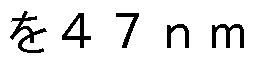 とし、
とし、
 バッファ層の膜 厚 2を〇〜 4 7 n
 まで変化させたときの、 吸収体膜の表面での巳 II V光 の反射率 (%) を示す図である。
[図 5]〇 「 1\1吸収層の膜厚を 1、 丁 3巳〇バッファ層の膜厚を 2とし、 バ ッファ層の膜厚 ¢1 2を 2〜 2 0 の範囲で変化させたときの、 吸収体膜の
\¥0 2020/175354 8 卩(:171? 2020 /007002
膜厚 0 (= 1 + 0^ 2、 n m) と、 吸収体膜の表面での巳 II V光の反射率 ( %) との関係を示す図である。
[図 6]〇 「 1\1吸収層の膜厚を 1、 丁 3巳〇バッファ層の膜厚を 2とし、 吸 収体膜の膜厚口 (= 1 + 2)
 とし、 丁 3巳〇バッファ層の膜 厚 2を〇〜 4 7 n
 まで変化させたときの、 吸収体膜の表面での巳 II V光 の反射率 (%) を示す図である。
[図 7]シミュレーションによって得られた吸収体膜 (吸収層/バッファ層) の 膜厚 0 (= 1 + 2) と、 吸収体膜の表面での巳 II V光の反射率 (%) と の関係を示す図である。
発明を実施するための形態
[0031] 以下、 本発明の実施形態について、 図面を参照しながら具体的に説明する 。 なお、 以下の実施形態は、 本発明を具体化する際の一形態であって、 本発 明をその範囲内に限定するものではない。 なお、 図中、 同一又は相当する部 分には同一の符号を付してその説明を簡略化ないし省略することがある。 [0032] <反射型マスクブランク 1 0 0の構成及びその製造方法 >
図 1は、 本発明の実施形態の反射型マスクブランク 1 〇〇の構成を説明す るための要部断面模式図である。 同図に示されるように、 反射型マスクブラ ンク 1 0 0は、 基板 1 と、 第 1主面 (表面) 側に形成された露光光である巳 II V光を反射する多層反射膜 2と、 当該多層反射膜 2を保護するために設け られる保護膜 3と、 巳 II V光を吸収する吸収体膜 4と、 エッチングマスク膜 6とを有し、 これらがこの順で積層される。 本実施形態の反射型マスクブラ ンク 1 0 0では、 吸収体膜 4が、 バッファ層 4 2と、 バッファ層 4 2の上に 設けられた吸収層 4 4とを有する。 また、 基板 1の第 2主面 (裏面) 側には 、 静電チャック用の裏面導電膜 5が形成される。
[0033] また、 上記反射型マスクブランク 1 0 0は、 裏面導電膜 5が形成されてい ない構成を含む。 更に、 上記反射型マスクブランク 1 〇〇は、 エッチングマ スク膜 6の上にレジスト膜 1 1 を形成したレジスト膜付きマスクブランクの 構成を含む。
\¥0 2020/175354 9 卩(:171? 2020 /007002
[0034] 本明細書において、 例えば、 「基板 1の主表面の上に形成された多層反射 膜 2」 との記載は、 多層反射膜 2が、 基板 1の表面に接して配置されること を意味する場合の他、 基板 1 と、 多層反射膜 2との間に他の膜を有すること を意味する場合も含む。 他の膜についても同様である。 また、 本明細書にお いて、 例えば 「膜八が膜巳の上に接して配置される」 とは、 膜八と膜巳との 間に他の膜を介さずに、 膜八と膜巳とが直接、 接するように配置されている ことを意味する。
[0035] 以下、 反射型マスクブランク 1 0 0の各構成について具体的に説明をする
[0036] «基板 1 >>
基板 1は、 巳 II V光による露光時の熱による吸収体パターン 4 3の歪みを 防止するため、 0 ± 5 匕/°〇の範囲内の低熱膨張係数を有するものが好 ましく用いられる。 この範囲の低熱膨張係数を有する素材としては、 例えば . 3 I 〇2 _丁 丨 〇2系ガラス、 多成分系ガラスセラミックス等を用いること ができる。
[0037] 基板 1の転写パターン (後述の吸収体膜 4をパターニングしたものがこれ を構成する) が形成される側の第 1主面は、 少なくともパターン転写精度、 位置精度を得る観点から高平坦度となるように表面加工されている。 巳 II V 露光の場合、

の領域において、 平坦度が 0 . 1 以下であることが好ましく
、 更に好ましくは〇. 0 5 以下、 特に好ましくは〇. 0 3 以下であ る。 また、 吸収体膜 4が形成される側と反対側の第 2主面は、 露光装置にセ ッ トするときに静電チヤックされる面であって、 1 4 2 01 111 X 1 4 2〇1 111の 領域において、 平坦度が〇. 1 以下であることが好ましく、 更に好まし くは〇. 0 5 〇1以下、 特に好ましくは〇. 0 3 〇1以下である。
[0038] また、 基板 1の表面平滑度の高さも極めて重要な項目である。 転写用吸収 体パターン 4 3が形成される基板 1の第 1主面の表面粗さは、 二乗平均平方 根粗さ
 で 0 . 1 n 以下であることが好ましい。 なお、 表面平滑
\¥0 2020/175354 10 卩(:171? 2020 /007002
で 0 . 1 n 以下であることが好ましい。 なお、 表面平滑
\¥0 2020/175354 10 卩(:171? 2020 /007002
度は、 原子間力顕微鏡で測定することができる。
[0039] 更に、 基板 1は、 その上に形成される膜 (多層反射膜 2など) の膜応力に よる変形を防止するために、 高い剛性を有しているものが好ましい。 特に、
6 5◦ 3以上の高いヤング率を有しているものが好ましい。
[0040] «多層反射膜 2 »
多層反射膜 2は、 反射型マスク 2 0 0において、 巳 II V光を反射する機能 を付与するものであり、 屈折率の異なる元素を主成分とする各層が周期的に 積層された多層膜の構成となっている。
[0041 ] 一般的には、 高屈折率材料である軽元素又はその化合物の薄膜 (高屈折率 層) と、 低屈折率材料である重元素又はその化合物の薄膜 (低屈折率層) と が交互に 4 0から 6 0周期程度積層された多層膜が、 多層反射膜 2として用 いられる。 多層膜は、 基板 1側から高屈折率層と低屈折率層をこの順に積層 した高屈折率層/低屈折率層の積層構造を 1周期として複数周期積層しても よい。 また、 多層膜は、 基板 1側から低屈折率層と高屈折率層をこの順に積 層した低屈折率層/高屈折率層の積層構造を 1周期として複数周期積層して もよい。 なお、 多層反射膜 2の最表面の層、 即ち多層反射膜 2の基板 1 と反 対側の表面層は、 高屈折率層とすることが好ましい。 上述の多層膜において 、 基板 1から高屈折率層と低屈折率層をこの順に積層した高屈折率層/低屈 折率層の積層構造を 1周期として複数周期積層する場合は最上層が低屈折率 層となる。 この場合、 低屈折率層が多層反射膜 2の最表面を構成すると容易 に酸化されてしまい反射型マスク 2 0 0の反射率が減少する。 そのため、 最 上層の低屈折率層上に高屈折率層を更に形成して多層反射膜 2とすることが 好ましい。 一方、 上述の多層膜において、 基板 1側から低屈折率層と高屈折 率層をこの順に積層した低屈折率層/高屈折率層の積層構造を 1周期として 複数周期積層する場合は、 最上層が高屈折率層となるので、 そのままでよい
[0042] 本実施形態において、 高屈折率層としては、 ケイ素 (3 丨) を含む層が採 用される。 3 丨 を含む材料としては、 3 丨単体の他に、 3 丨 に、 ボロン (巳
\¥0 2020/175354 1 1 卩(:171? 2020 /007002
) 、 炭素 (<3) 、 窒素 (1\1) 、 及び酸素 (〇) を含む 3 丨化合物でもよい。
3 丨 を含む層を高屈折率層として使用することによって、
 光の反射率 に優れた
 リソグラフィ用反射型マスク 2 0 0が得られる。 また、 本実 施形態において基板 1 としてはガラス基板が好ましく用いられる。 3 丨 はガ ラス基板との密着性においても優れている。 また、 低屈折率層としては、 モ リブデン (1\/1〇) 、 ルテニウム ([¾リ) 、 ロジウム
 及び白金 ( 1:) から選ばれる金属単体、 又はこれらの合金が用いられる。 例えば波長 1 3 n mから 1 4 n の巳 II V光に対する多層反射膜 2としては、 好ましくは !\/!〇膜と 3 丨膜を交互に 4 0から 6 0周期程度積層した IV!〇/ 3 丨周期積層 膜が用いられる。 なお、 多層反射膜 2の最上層である高屈折率層をケイ素 ( 3 I) で形成し、 当該最上層 (3 丨) と リ系保護膜 3との間に、 ケイ素と 酸素とを含むケイ素酸化物層を形成するようにしてもよい。 これにより、 マ スク洗浄耐性を向上させることができる。
[0043] このような多層反射膜 2の単独での反射率は通常 6 5 %以上であり、 上限 は通常 7 3 %である。 なお、 多層反射膜 2の各構成層の厚み及び周期は、 露 光波長により適宜選択すればよく、 ブラッグ反射の法則を満たすように選択 される。 多層反射膜 2において高屈折率層及び低屈折率層はそれぞれ複数存 在する。 高屈折率層同士、 そして低屈折率層同士の厚みが同じでなくてもよ い。 また、 多層反射膜 2の最表面の 3 丨層の膜厚は、 反射率を低下させない 範囲で調整することができる。 最表面の 3 丨 (高屈折率層) の膜厚は、 3 n
 とすることができる。
[0044] 多層反射膜 2の形成方法は当該技術分野において公知である。 例えばイオ ンビームスパッタリング法により、 多層反射膜 2の各層を成膜することで形 成できる。 上述した
 丨周期多層膜の場合、 例えばイオンビームスパ ッタリング法により、 先ず 3 丨 夕ーゲッ トを用いて厚さ 4 n 程度の 3 丨膜 を基板 1上に成膜し、 その後 IV!〇夕ーゲッ トを用いて厚さ 3 n 程度の 1\/1〇 月莫を成膜し、 これを 1周期として、 4 0から 6 0周期積層して、 多層反射膜 2を形成する (最表面の層は 3 丨層とする) 。 また、 多層反射膜 2の成膜の
\¥0 2020/175354 12 卩(:17 2020 /007002
丨周期多層膜の場合、 例えばイオンビームスパ ッタリング法により、 先ず 3 丨 夕ーゲッ トを用いて厚さ 4 n 程度の 3 丨膜 を基板 1上に成膜し、 その後 IV!〇夕ーゲッ トを用いて厚さ 3 n 程度の 1\/1〇 月莫を成膜し、 これを 1周期として、 4 0から 6 0周期積層して、 多層反射膜 2を形成する (最表面の層は 3 丨層とする) 。 また、 多層反射膜 2の成膜の
\¥0 2020/175354 12 卩(:17 2020 /007002
際に、 イオン源からクリプトン ([< !〇 イオン粒子を供給して、 イオンビー 厶スパッタリングを行うことにより多層反射膜 2を形成することが好ましい
[0045] «保護膜 3 »
本実施形態の反射型マスクブランク 1 〇〇は、 多層反射膜 2と吸収体膜 4 との間に、 保護膜 3を有することが好ましい。 多層反射膜 2上に保護膜 3が 形成されていることにより、 反射型マスクブランク 1 0 0を用いて反射型マ スク 2 0 0 (巳 II Vマスク) を製造する際の多層反射膜 2表面へのダメージ を抑制することができるので、 巳 II V光に対する反射率特性が良好となる。
[0046] 保護膜 3は、 後述する反射型マスク 2 0 0の製造工程におけるドライエッ チング及び洗浄から多層反射膜 2を保護するために、 多層反射膜 2の上に形 成される。 また、 電子線 (巳巳) を用いた吸収体パターン 4 3の黒欠陥修正 の際の多層反射膜 2の保護も兼ね備える。 保護膜 3は、 エッチャント、 及び 洗浄液等に対して耐性を有する材料で形成される。 ここで、 図 1では保護膜 3が 1層の場合を示しているが、 3層以上の積層構造とすることもできる。 例えば、 最下層と最上層を、 上記[^ 1·!を含有する物質からなる層とし、 最下 層と最上層との間に、
 以外の金属、 若しくは合金を介在させた保護膜 3 としても構わない。 例えば、 保護膜 3は、 ルテニウムを主成分として含む材 料により構成されることもできる。 すなわち、 保護膜 3の材料は、 [¾リ金属 単体でもよいし、 [¾リにチタン (丁 丨) 、 ニオブ
 モリブデン (IV! 〇) 、 ジルコニウム ( 〇 、 イッ トリウム (丫) 、 ホウ素 (巳) 、 ランタ ン (1 - 3) 、 コバルト (〇〇) 、 及びレニウム
 などから選択される 少なくとも 1種の金属を含有した 8リ合金であってよく、 窒素を含んでいて も構わない。 このような保護膜 3は、 特に、 吸収体膜 4のうちのバッファ層 4 2を、 塩素系ガス (〇 I系ガス) のドライエッチングでバターニングする 場合に有効である。 保護膜 3は、 塩素系ガスを用いたドライエッチングにお ける保護膜 3に対する吸収体膜 4のエッチング選択比 (吸収体膜 4のエッチ ング速度/保護膜 3のエッチング速度) が 1 . 5以上、 好ましくは 3以上と
\¥0 2020/175354 13 卩(:171? 2020 /007002
などから選択される 少なくとも 1種の金属を含有した 8リ合金であってよく、 窒素を含んでいて も構わない。 このような保護膜 3は、 特に、 吸収体膜 4のうちのバッファ層 4 2を、 塩素系ガス (〇 I系ガス) のドライエッチングでバターニングする 場合に有効である。 保護膜 3は、 塩素系ガスを用いたドライエッチングにお ける保護膜 3に対する吸収体膜 4のエッチング選択比 (吸収体膜 4のエッチ ング速度/保護膜 3のエッチング速度) が 1 . 5以上、 好ましくは 3以上と
\¥0 2020/175354 13 卩(:171? 2020 /007002
なる材料で形成されることが好ましい。
[0047] この リ合金の リ含有量は 5 0原子%以上 1 0 0原子%未満、 好ましく は 8 0原子%以上 1 0 0原子%未満、 更に好ましくは 9 5原子%以上 1 0 0 原子%未満である。 特に、
 リ合金の リ含有量が 9 5原子%以上 1 0 0原 子%未満の場合は、 保護膜 3への多層反射膜 2構成元素 (ケイ素) の拡散を 抑えつつ、
 光の反射率を十分確保することができる。 更に、 この保護 膜 3の場合は、 マスク洗浄耐性、 吸収体膜 4 (具体的には、 バッファ層 4 2 ) をエッチング加工したときのエッチングストッパー機能、 及び多層反射膜 2の経時変化防止の保護膜機能を兼ね備えることが可能となる。
[0048] 巳 II Vリソグラフイでは、 露光光に対して透明な物質が少ないので、 マス クパターン面への異物付着を防止する巳 II Vペリクルが技術的に簡単ではな い。 このことから、 ペリクルを用いないペリクルレス運用が主流となってい る。 また、 巳 11 リソグラフイでは、 巳 II V露光によってマスクに力ーボン 膜が堆積したり、 酸化膜が成長したりするといった露光コンタミネーション が起こる。 そのため、 巳 II V反射型マスク 2 0 0を半導体装置の製造に使用 している段階で、 度々洗浄を行ってマスク上の異物やコンタミネーションを 除去する必要がある。 このため、 巳 II V反射型マスク 2 0 0では、 光リソグ ラフイ用の透過型マスクに比べて桁違いのマスク洗浄耐性が要求されている 。 丁 丨 を含有した リ系保護膜 3を用いると、 硫酸、 硫酸過水 (3 1\/1) 、 アンモニア、 アンモニア過水 (八 1\/1) 、 〇1~1ラジカル洗浄水、 又は濃度が 1 〇 以下のオゾン水などの洗浄液に対する洗浄耐性が特に高く、 マス ク洗浄耐性の要求を満たすことが可能となる。
[0049] このような リ又はその合金などにより構成される保護膜 3の厚みは、 そ の保護膜 3としての機能を果たすことができる限り特に制限されない。 巳 II V光の反射率の観点から、 保護膜 3の厚みは、 好ましくは、 1 . O n mから 8 . 0门〇1、 より好ましくは、 ·! . 5 1^ 111から 6 . 0门 である。
[0050] 保護膜 3の形成方法としては、 公知の膜形成方法と同様のものを特に制限 なく採用することができる。 具体例としては、 スパッタリング法及びイオン
\¥0 2020/175354 14 卩(:171? 2020 /007002
ビームスパッタリング法が挙げられる。
[0051 ] «吸収体膜 4 »
本実施形態の反射型マスクブランク 1 〇〇では、 多層反射膜 2又は保護膜 3の上に、 日 II V光を吸収する吸収体膜 4が形成される。 吸収体膜 4は、 巳 II V光を吸収する機能を有する。 本実施形態の吸収体膜 4は、 バッファ層 4 2と、 バッファ層 4 2の上 (基板 1 とは反対側) に設けられた吸収層 4 4と を有する。 本実施形態の反射型マスクブランク 1 0 0は、 タンタル (丁
 又はケイ素 (3 丨) を含有する材料からなるバッファ層 4 2及びクロム (〇 「) を含有する材料からなる吸収層 4 4を含む吸収体膜 4、 並びに後述する 所定の材料のエッチングマスク膜 6を含むことにより、 レジスト膜 1 1及び 吸収体膜 4の薄膜化が可能となる。
[0052] 後述するように、 本実施形態の吸収体膜 4のうち、 吸収層 4 4は、
 を 含有する材料からなる。
 を含有する薄膜が、 [¾リを主材料とする保護膜 3の表面に接して配置される場合、 吸収層 4 4と保護膜 3のエッチング選択 比が高くないという問題が生じる。 そのため、 本実施形態の吸収体膜 4では 、 吸収層 4 4と保護膜 3との間に、 所定の材料のバッファ層 4 2を配置する ことにした。
[0053] 本実施形態の反射型マスクブランク 1 〇〇の吸収体膜 4を構成するバッフ ァ層 4 2及び吸収層 4 4の膜厚を得るために、 図 3〜 6に示すようなシミュ レーシヨンを行なつた。 巳 II V光における吸収体膜 4の反射率が 2 %以下で あれば、 半導体装置のリソグラフィのための反射型マスク 2 0 0として用い ることができる。
[0054] 図 3〜 6に示すシミュレーシヨンに用いた構造は、

周期膜の多層反射膜 2、 及びルテニウムを材料とする保護膜 3 (膜厚: 3 . 5门〇〇 が形成され、 さらにその上にバッファ層 4 2 (膜厚: 2) 及び吸 収層 4 4 (膜厚: 1) を形成した構造である。 IV!〇/ 3 丨周期膜の多層反 射膜 2は、 3 丨層の膜厚を 4 . 2 n m、 1\/1〇層の膜厚を 2 . 8 n とし、 基 板 1の上に単層の 3 丨層及び単層の IV!〇層を 1周期として 4 0周期積層し、
\¥0 2020/175354 15 卩(:171? 2020 /007002
最上層として膜厚が 4 . 0 n の 3 丨層を配置した構造とした。 また、 吸収 体膜 4 (吸収層 4 4 /バッファ層 4 2) の膜厚を口 (= 6 ^ + 6 2) とした 。 なお、 本構造は、 反射型マスク 2 0 0を製造したときの、 吸収体膜 4の反 射率と、 バッファ層 4 2及び吸収層 4 4の膜厚との関係を考察するものなの で、 エッチングマスク膜 6は配置されない構造とした。 反射型マスク 2 0 0 を製造する際には、 エッチングマスク膜 6は最終的に除去されるからである
[0055] 図 3に、 吸収層 4 4 (材料:
 の膜厚を 1、 バッファ層 4 2 (材 料: 丁 3巳 1\!) の膜厚を 2とし、 バッファ層 4 2の膜厚 2を 2〜 2 0 n の範囲で変化させたときの、 吸収体膜 4の膜厚口 (=〇1 1 +〇1 2、 1^ 01) と、 吸収体膜 4の表面での巳 II V光の反射率 (%) との関係を示す。 図 3に 示すように、 膜厚口に伴う巳 II V光の干渉のため、 反射率は、 膜厚口の変化 に対して振動的な振る舞いを示す。 また、 図 3から明らかなように、 〇 「 の吸収層 4 4及び丁 3巳 1\1のバッファ層 4 2を有する吸収体膜 4の場合には 、 吸収体膜 4が 4 7 n 付近になったときに巳 II V光の反射率が 2 %以下と なる極小値、 5 5 n 付近になったときに反射率が 1 %以下となる極小値を 取ることが理解できる。 なお、 図 3に用いた構造の場合には、 2 %以下の巳 リ 光の反射率を得るために、 吸収体膜 4の膜厚 0は、 少なくとも 4 6 n 程度以上必要であることが理解できる。
[0056] 図 3において、 吸収体膜 4が 4 7 n 付近になったときに反射率が 2 %以 下となる極小値を取ることから、 さらに吸収体膜 4の膜厚が 4 7 n の場合 について、 考察する。 図 4は、 吸収体膜 4の膜厚 0 (= 6 ^ + 6 2) を 4 7 バッファ層 4 2 (材料: 丁 3巳 1\1) の膜厚 2を〇〜 4 7门〇1ま で変化させたときの、 吸収体膜 4の表面での巳 II V光の反射率 (%) を示す 。 なお、 バッファ層 4 2の膜厚 2の変化に伴い、 吸収層 4 4 (材料:
 ) の膜厚 ¢1 1は、
 まで変化することになる。 図 4に示すよう に、 吸収体膜 4の膜厚 0 (= 6 ^ + 6 2) を 4 7 n mとした場合、 バッファ 層 4 2 (材料: 丁 3巳 1\1) の膜厚 2が〇〜 2 4 n 付近 (概ね膜厚 2が
\¥0 2020/175354 16 卩(:171? 2020 /007002
まで変化することになる。 図 4に示すよう に、 吸収体膜 4の膜厚 0 (= 6 ^ + 6 2) を 4 7 n mとした場合、 バッファ 層 4 2 (材料: 丁 3巳 1\1) の膜厚 2が〇〜 2 4 n 付近 (概ね膜厚 2が
\¥0 2020/175354 16 卩(:171? 2020 /007002
〇〜 2 5 n m付近) までの範囲で、 巳 II V光の反射率が 2 %以下となること が理解できる。 したがって、 丁 3巳 1\1のバッファ層 4 2の膜厚 2が 2 5门 以下であれば、 巳 II V光の反射率が 2 %以下という要求を満足することが できる。
[0057] 図 5に、 バッファ層 4 2の材料を丁 3巳〇とした他は、 図 3の場合と同様 の、 吸収体膜 4の膜厚 0
 と、 吸収体膜 4の表面での巳 II V光の反射 率 (%) との関係を示す。 すなわち、 図 5に、 吸収層 4 4 (材料: 〇 「 1\1) の膜厚を 1、 バッファ層 4 2 (材料: 丁 3巳〇) の膜厚を 2とし、 バッ
 の範囲で変化させたときの、 吸収体膜
4の膜厚口 (= 6 ^ + 6 2. n m) と、 吸収体膜 4の表面での巳 II V光の反 射率 (%) との関係を示す。 図 3と同様に、 図 5では、

光の干渉のため、 反射率は、 膜厚口の変化に対して振動的な振る舞いを示す 。 また、 図 5から明らかなように、 〇 「 1\1の吸収層 4 4及び丁 8巳〇のバッ ファ層 4 2を有する吸収体膜 4の場合には、 吸収体膜 4が 4 7 n 付近にな ったときに巳 II V光の反射率が 2 %以下となる極小値、
 付近になっ たときに反射率が 1 %以下となる極小値を取ることが理解できる。 なお、 図 5に用いた構造の場合には、 2 %以下の巳 II V光の反射率を得るために、 丁 3巳〇バッファ層の膜厚が 1 0 n
 以下のときに、 吸収体膜 4の膜厚 0は、 少なくとも 4 6 n 程度以上必要であることが理解できる。
[0058] 図 5において、 吸収体膜 4が 4 7 n 付近になったときに反射率が 2 %以 下となる極小値を取ることから、 図 4の場合と同様に、 さらに吸収体膜 4の 膜厚が
 の場合について、 考察する。 図 4の場合と同様に、 図 6は、 吸収体膜 4の膜厚 0 (= 1 + 2) を 4 7 n mとし、 バッファ層 4 2 (材 料: 丁 3巳〇)
 まで変化させたときの、 吸収体膜 4の表面での巳 II V光の反射率 (%) を示す。 なお、 バッファ層 4 2の膜厚 2の変化に伴い、 吸収層 4 4 (材料: 0 「 1\1) の膜厚 1は、 4 7 ~ 0 n まで変化することになる。 図 6に示すように、 吸収体膜 4の膜厚 0 (= 1 + 2)
 した場合、 バッファ層 4 2 (材料: 丁 3巳〇) の膜
\¥0 2020/175354 17 卩(:171? 2020 /007002
した場合、 バッファ層 4 2 (材料: 丁 3巳〇) の膜
\¥0 2020/175354 17 卩(:171? 2020 /007002
厚 2が〇〜 1 4 n 付近 (概ね〇〜 付近) までの範囲で、 º II V 光の反射率が 2 %以下となることが理解できる。 したがって、 丁 3巳〇のバ ッファ層 4 2の膜厚 2が 1 5 n 以下であれば、 巳 II V光の反射率が 2 % 以下という要求を満足することができる。
[0059] 図 7に、 シミュレーションによって得られた吸収体膜 4 (吸収層 4 4 /バ ッファ層 4 2) の膜厚 0 (= 1 +〇^ 2) と、 吸収体膜

光の反射率 (〇/〇) との関係を示す。 シミュレーションに用いた構造は、 基板 1
 丨周期膜の多層反射膜 2、 及びルテニウムを材料とする保護 膜 3 (3 . 5 n m) が形成され、 さらにその上にバッファ層 4 2 (膜厚: 2 = 2 n m) 及び吸収層 4 4 (膜厚: 1) を形成した構造である。 なお、 IV!〇/ 3 丨周期膜の多層反射膜 2は、 上述の図 3〜 6のシミュレーションと 同様の構造とした。 バッファ層 4 2の材料は、 丁 3巳 1\1及び丁 3巳〇とした 。 参考のために、 バッファ層 4 2を有しない、 従来の構造である丁 3巳 1\1膜 単層の吸収体膜 4の膜厚 0と、 吸収体膜 4の表面での日 II V光の反射率 (% ) との関係を示す。 図 7から、 0 「 1\1吸収層 4 4を有する吸収体膜 4 (吸収 層 4 4 /バッファ層 4 2) の場合には、 従来の丁 3巳 1\1膜単層の吸収体膜 4 と比べて、 巳 II V光の反射率 (%) が大きく低下していることが見て取れる 。 したがって、 本実施形態の吸収体膜 4を用いることにより、 従来より薄い 吸収体膜 4の場合であっても 2 %以下の反射率を達成できることが理解でき る。
[0060] また、 バッファ層 4 2として機能を有するためには、 バッファ層 4 2の膜 厚が〇. 5 n 以上であることが必要である。 したがって、 本実施形態の反 射型マスクブランク 1 0 0において、 バッファ層 4 2が、 タンタル (丁 8) を含有する材料からなる場合には、 2 %以下の反射率を達成するために、 バ ッファ層 4 2の膜厚を 0 .
 以下にすることが必要である といえる。
[0061 ] 以上のシミュレーションの結果から、 バッファ層 4 2の材料として丁 3巳
!\1及び丁 3巳〇を用いた場合に、 所定の膜厚の範囲であれば、 従来より薄い
\¥0 2020/175354 18 卩(:171? 2020 /007002
吸収体膜 4の場合であっても 2 %以下の反射率を達成できることについて説 明した。 同様のシミュレーションを、 バッファ層 4 2の材料としてケイ素 ( 3 丨) を含有する材料を用いた場合について行い、 同様の結果を得た。
[0062] すなわち、 上述と同様のシミュレーションにより、 本実施形態の反射型マ スクブランク 1 0 0において、 バッファ層 4 2が、 ケイ素 (3 丨) を含有す る材料からなる場合にも、 2 %以下の反射率を達成するために、 バッファ層 4 2の膜厚を〇.

を得た。 また、 バッファ層 4 2が、 ケイ素 (3 丨) を含有する材料からなる 場合にも、 2 %以下の巳 II V光の反射率を得るために、 吸収体膜 4の膜厚 0 は、 少なくとも 4 6
 程度以上必要であるとの結果を得た。
[0063] 次に、 バッファ層 4 2がタンタル (丁 3) を含有する材料からなる場合に ついて、 さらに説明する。
[0064] 本実施形態の反射型マスクブランク 1 0 0は、 バッファ層 4 2の材料が、 タンタル
 と、 酸素 (〇) 、 窒素 (1\!) 、 炭素 (〇 、 ホウ素 (巳) 及び水素 (|~|) から選らばれる 1以上の元素とを含有する材料であることが 好ましい。 また、 バッファ層 4 2の材料は、 タンタル
 と、 酸素 (〇 ) 、 窒素 (1\〇 、 ホウ素 (巳) 及び水素 (1~1) から選らばれる 1以上の元素 とを含有する材料であることがより好ましい。 上述のシミュレーション結果 から明らかなように、 バッファ層 4 2の材料を、 所定のタンタル (丁 3) 系 材料とすることにより、 従来より薄い吸収体膜 4の場合であっても 2 %以下 の反射率を達成できる。
[0065] また、 バッファ層 4 2の材料が所定のタンタル (丁 3) を含む材料である ことにより、 クロム (〇 「) を含有する材料からなる吸収層 4 4のエッチン グの際に、 バッファ層 4 2のエッチングが実質的になされないエッチングガ スを選択することができる。
[0066] 本実施形態の反射型マスクブランク 1 0 0は、 バッファ層 4 2の材料が、 タンタル (丁
 と、 窒素 (1\!) 及びホウ素 (巳) から選ばれる少なくとも —つの元素とを含み、 バッファ層
 以下であることが好
\¥0 2020/175354 19 卩(:171? 2020 /007002
以下であることが好
\¥0 2020/175354 19 卩(:171? 2020 /007002
ましい。 また、 図 4に示すように、 バッファ層 4 2の膜厚が薄い方が、 巳 II V光反射率をより低くすることができると共に、 膜厚に対する振動を小さく することができる。 そのため、 バッファ層 4 2の膜厚は、 1 5 n m以下がよ り好ましく、 1 〇门 以下がさらに好ましく、 4 n 未満が特に好ましい。 なお、 バッファ層 4 2の材料は、 タンタル (丁
 及び窒素 (1\1) を含み、 ホウ素 (巳) を含まないようにしてもよい。 また、 バッファ層 4 2の材料は 、 タンタル (丁
 及びホウ素 (巳) を含み、 窒素 (1\1) を含まないように してもよい。 バッファ層 4 2の材料をタンタル
 と、 窒素 (1\1) 及び ホウ素 (巳) から選ばれる少なくとも一つの元素とを含む材料とすることに より、 吸収層 4 4がクロム (〇 〇 を含有する材料からなる層である場合で も、 保護膜 3と、 吸収層 4 4との間のエッチング選択比に関する問題を回避 し、 適切なエッチングガスを選択することができる。 また、 吸収体膜 4の膜 厚を薄くすることができるので、 反射型マスク 2 0 0のシャドーイング効果 をより低減することができる。
[0067] バッファ層 4 2中のタンタル含有量は、 5 0原子%以上であることが好ま しく、 7 0原子%以上であることがより好ましい。 バッファ層 4 2中のタン タル含有量は、 9 5原子%以下であることが好ましい。 バッファ層 4 2中の 窒素とホウ素の合計含有量は、 5 0原子%以下であることが好ましく、 3 0 原子%以下であることがより好ましい。 バッファ層 4 2中の窒素とホウ素の 合計含有量は、 5原子%以上であることが好ましい。 窒素の含有量はホウ素 の含有量よりも少ない方が好ましい。 窒素の含有量が少ない方が塩素ガスで のエッチングレートが速くなり、 バッファ層 4 2を除去しやすいからである 。 バッファ層 4 2中の水素含有量は、 〇. 1原子%以上であることが好まし く、 5原子%以下であることが好ましく、 3原子%以下であることがより好 ましい。
[0068] タンタル (丁
 と、 窒素 (1\!) 及びホウ素 (巳) から選ばれる少なくと も一つの元素とを含有する材料からなる本実施形態のバッファ層 4 2は、 フ ッ素系ガス又は酸素を含まない塩素系ガスによりエッチングすることができ
\¥0 2020/175354 20 卩(:17 2020 /007002
と、 窒素 (1\!) 及びホウ素 (巳) から選ばれる少なくと も一つの元素とを含有する材料からなる本実施形態のバッファ層 4 2は、 フ ッ素系ガス又は酸素を含まない塩素系ガスによりエッチングすることができ
\¥0 2020/175354 20 卩(:17 2020 /007002
る。
[0069] フッ素系ガスとしては、 〇 4、 〇1~1 3、 〇2 6、 〇3 6、 〇4 6、 〇4
8、 〇1~1 2 2、 〇1~1 3 、 〇3 8、 3 6、 及び 1= 2等を用いることができる 〇 塩素系ガスとしては、 〇 丨 2、 3 I 0 I 4, 〇1~1〇 丨 3、 〇〇 丨 4、 及び巳〇 I 3等を用いることができる。 また、 これらのエッチングガスは、 必要に応じ て、 更に、 1~1 6及び/又は八 「などの不活性ガスを含むことができる。
[0070] 本実施形態の反射型マスクブランク 1 0 0は、 バッファ層 4 2の材料が、 タンタル (丁 3) 及び酸素 (〇) を含み、 バッファ層 4 2の膜厚が 1 5 n m 以下であることが好ましい。 また、 図 6に示すように、 バッファ層 4 2の膜 厚が薄い方が、
 光反射率をより低くすることができると共に、 膜厚に 対する振動を小さくすることができるため、 バッファ層 4 2の膜厚は、 1 0 门 以下がより好ましく、 4 n 未満がさらに好ましい。 なお、 バッファ層 4 2の材料は、 タンタル (丁
 及び酸素 (〇) の他、 ホウ素 (巳) 及び/ 又は水素 (1~1) を含むことができる。 バッファ層 4 2の材料をタンタル (丁 a) 及び酸素 (〇) を含む材料とすることにより、 吸収層 4 4がクロム (〇 「) を含有する材料からなる層である場合でも、 保護膜 3と、 吸収層 4 4と の間のエッチング選択比に関する問題を回避し、 適切なエッチングガスを選 択することができる。 また、 吸収体膜 4の膜厚を薄くすることができるので 、 反射型マスク 2 0 0のシャドーイング効果をより低減することができる。
[0071 ] バッファ層 4 2中のタンタル含有量は、 5 0原子%以上であることが好ま しく、 7 0原子%以上であることがより好ましい。 バッファ層 4 2中のタン タル含有量は、 9 5原子%以下であることが好ましい。 バッファ層 4 2中の 酸素含有量は、 7 0原子%以下であることが好ましく、 6 0原子%以下であ ることがより好ましい。 バッファ層 4 2中の窒素含有量は、 エッチング容易 性の観点から 1 〇原子%以上であることが好ましい。 バッファ層 4 2中の水 素含有量は、 〇. 1原子%以上であることが好ましく、 5原子%以下である ことが好ましく、 3原子%以下であることがより好ましい。
[0072] タンタル (丁
 及び酸素 (〇) を含有する材料からなる本実施形態のバ
\¥0 2020/175354 21 卩(:171? 2020 /007002
及び酸素 (〇) を含有する材料からなる本実施形態のバ
\¥0 2020/175354 21 卩(:171? 2020 /007002
ッファ層 4 2は、 上述のフッ素系ガスによりエッチングすることができる。
[0073] 次に、 バッファ層 4 2がケイ素を含有する材料からなる場合について説明 する。
[0074] 本実施形態の反射型マスクブランク 1 0 0は、 バッファ層 4 2の材料が、 ケイ素、 ケイ素化合物、 ケイ素及び金属を含む金属ケイ素、 又はケイ素化合 物及び金属を含む金属ケイ素化合物の材料であり、 ケイ素化合物の材料が、 ケイ素と、 酸素 (〇) 、 窒素 (1\〇 、 炭素 (〇 及び水素 (! !) から選ばれ る少なくとも一つの元素とを含むことが好ましい。 また、 エッチングマスク 膜 6の材料のうちケイ素化合物の材料が、 ケイ素と、 酸素 (〇) 及び窒素 ( 1\〇 から選ばれる少なくとも一つの元素とを含むことがより好ましい。
[0075] ケイ素を含む材料として、 具体的には、 3 I 0 , 3 丨 1\1、 3 丨 〇1\1、 3 I 〇、 3 I 0 0 , 3 丨 〇1\1、 3 丨 〇〇1\1、 1\/1〇 3 丨、 1\/1〇 3 丨 〇、 1\/1〇 3 丨 、 及び 1\/1〇 3 丨 〇 1\!等を挙げることができる。 ケイ素を含む材料として、 3 I 0 , 3 I 1\1又は 3 丨 〇 1\!を用いることが好ましい。 なお、 材料は、 本発明 の効果が得られる範囲で、 ケイ素以外の半金属又は金属を含有することがで きる。 また、 金属ケイ素化合物としては、 モリブデンシリサイ ドを用いるこ とができる。
[0076] 上述のタンタル系材料のバッファ層 4 2の場合と同様に、 バッファ層 4 2 がケイ素系の材料である場合にも、 保護膜 3と、 吸収層 4 4との間のエッチ ング選択比に関する問題を回避して、 吸収体膜 4の膜厚を薄くすることがで きる。 そのため、 反射型マスク 2 0 0のシャドーイング効果をより低減する ことができる。
[0077] バッファ層 4 2は、 後述するエッチングマスク膜 6と同じ材料で形成する ことが好ましい。 この結果、 バッファ層 4 2をバターニングしたときにエッ チングマスク膜 6を同時に除去できる。 また、 バッファ層 4 2とエッチング マスク膜 6とを同じ材料で形成し、 組成比を互いに異ならせてもよい。 また 、 バッファ層 4 2はタンタルを含有する材料で形成し、 エッチングマスク膜 6はケイ素を含有する材料で形成してもよい。 また、 バッファ層 4 2はケイ
\¥0 2020/175354 22 卩(:171? 2020 /007002
素を含有する材料で形成し、 エッチングマスク膜 6はタンタルを含有する材 料で形成してもよい。
[0078] バッファ層 4 2の膜厚は、 吸収体膜 4のエッチングの際に保護膜 3にダメ —ジを与えて光学特性が変わることを抑制する観点から、 〇. 5 n 以上で あり、 好ましくは 1 门 以上であり、 より好ましくは 2 n 以上である。 ま た、 バッファ層 4 2の膜厚は、 吸収体膜 4とバッファ層 4 2の合計膜厚を薄 くする、 即ち吸収体パターン 4 3の高さを低くする観点から、 2 5 n m以下 であることが好ましく、 1 5 n 以下がより好ましく、 1 0 n
 以下がさら に好ましく、 4
 未満であることが特に好ましい。
[0079] また、 バッファ層 4 2の消衰係数は、 〇. 0 1以上〇. 0 3 5未満とする ことができる。
[0080] また、 バッファ層 4 2及びエッチングマスク膜 6を同時にエッチングする 場合には、 バッファ層 4 2の膜厚は、 エッチングマスク膜 6の膜厚と同じで あること、 又はエッチングマスク膜 6の膜厚より薄いことが好ましい。 更に 、 (バッファ層 4 2の膜厚) £ (エッチングマスク膜 6の膜厚) の場合には 、 (バッファ層 4 2のエッチング速度) £ (エッチングマスク膜 6のエッチ ング速度) の関係を満たすことが好ましい。
[0081 ] ケイ素を含有する材料からなるバッファ層 4 2は、 フッ素系ガスによりエ ッチングすることができる。
[0082] 次に、 本実施形態の吸収体膜 4に含まれる吸収層 4 4について説明する。
[0083] 実施形態の反射型マスクブランク 1 0 0では、 巳 II V光の吸収を、 主に吸 収層 4 4において行う。 そのため、 吸収層 4 4の材料は、 消衰係数が比較的 大きいクロム (〇 〇 を含有する材料からなる。 そのため、 吸収層 4 4の材 料は、 バッファ層 4 2よりも巳 II V光に対する消衰係数が大きい。 吸収層 4 4の消衰係数は、 〇. 0 3 5以上が好ましい。
[0084] 吸収層 4 4の材料は、 クロム (<3 〇 と、 窒素 (1\!) 及び炭素 (〇 から 選ばれる少なくとも一つの元素とを含む材料あることが好ましい。 なお、 吸 収層 4 4の材料は、 消衰係数 !<に対して悪影響を与えない範囲で、 クロム (
\¥0 2020/175354 23 卩(:171? 2020 /007002
〇 〇 、 窒素 (1\1) 及び炭素 (<3) 以外の成分、 例えば酸素 (0) 及び/又 は水素 (! !) 等を含むことができる。 消衰係数 1<が大きいクロム ((3 〇 を 含む所定の材料で吸収層 4 4を形成することにより、 タンタル (丁
 を含 む材料よりも消衰係数 1<が大きい吸収層 4 4を得ることができる。 そのため 、 吸収体膜 4の膜厚を薄くすることができるので、 反射型マスク 2 0 0のシ ャドーイング効果をより低減することができる。
[0085] 吸収層 4 4の材料は、 クロム (<3 〇 と、 窒素 (1\1) 及び炭素 (〇 から 選ばれる少なくとも一つの元素とを含むクロム化合物である。 クロム化合物 としては、 例えば、 〇 「 1\1、 〇 「〇、 〇 「〇 1\1、 〇 「〇〇、 〇 「〇 1\1、 〇 「 〇〇1\1、 〇 「巳1\1、 〇 巳〇、 〇 「巳〇1\1、 〇 「巳〇1\1及び〇 「巳〇〇1\1等 が挙げられる。 吸収層 4 4の消衰係数を大きくするためには、 酸素を含まな い材料とすることが好ましい。 この場合、 塩素系ガスに対するエッチング選 択比を上げることも可能である。 酸素を含まないクロム化合物として、 例え
 〇 「巳1\1、 〇 「巳〇及び〇 「巳〇 1\1等が挙げ られる。 クロム化合物の〇 「含有量は、 5 0原子%以上 1 0 0原子%未満で あることが好ましく、 8 0原子%以上 1 0 0原子%未満であることがより好 ましい。 クロム化合物の窒素 (1\!) 含有量は、 5原子%以上が好ましく、 2 0原子%以下が好ましく、 1 5原子%以下がより好ましい。 また、 本明細書 において、 「酸素を含まない」 とは、 クロム化合物における酸素の含有量が 1 〇原子%以下、 好ましくは 5原子%以下であるものが該当する。 なお、 材 料は、 本発明の効果が得られる範囲で、 クロム以外の金属を含有することが できる。
[0086] 本実施形態の反射型マスクブランク 1 0 0では、 吸収層 4 4の材料が、 ク ロム (<3 〇 及び窒素 (1\!) を含み、 吸収層 4 4の膜厚が 2 5 n 以上 6 0 〇!未満であることが好ましい。 また、 吸収層 4 4の膜厚の上限は、 5 0 1^ 未満であることがより好ましい。 また、 吸収層 4 4の膜厚の下限は、 3 5 门 以上であることがより好ましく、 4 5 n
 以上であることがさらに好ま しい。 吸収層 4 4の材料をクロム (<3 〇 及び窒素 (1\1) を含む材料とする
\¥0 2020/175354 24 卩(:171? 2020 /007002
以上であることがさらに好ま しい。 吸収層 4 4の材料をクロム (<3 〇 及び窒素 (1\1) を含む材料とする
\¥0 2020/175354 24 卩(:171? 2020 /007002
ことにより、 吸収層 4 4の膜厚を上記の膜厚にすることができるので、 吸収 体膜 4の膜厚を従来より薄くすることができる。 そのため、 反射型マスク 2 0 0のシャドーイング効果をより低減することができる。
[0087] クロム (〇 〇 を含有する材料からなる本実施形態の吸収層 4 4は、 上述 の塩素系ガス及び酸素ガスの混合ガスによりエッチングすることができる。
[0088] 巳 II V光の吸収を目的とした吸収体膜 4の場合、 吸収体膜 4に対する巳 II V光の反射率が 2 %以下、 好ましくは 1 %以下となるように、 膜厚が設定さ れる。 また、 シャドーイング効果を抑制するために、 吸収体膜 4の膜厚は、
6 0 n 未満、 好ましくは 5 0 n 以下とすることが求められる。
[0089] また、 吸収体膜 4 (吸収層 4 4) の表面には、 酸化層を形成してもよい。
吸収体膜 4 (吸収層 4 4) の表面に酸化層を形成することにより、 得られる 反射型マスク 2 0 0の吸収体パターン 4 3の洗浄耐性を向上させることがで きる。 酸化層の厚さは、 1 . 0 1·!〇!以上が好ましく、 1 .
 以上がより 好ましい。 また、 酸化層の厚さは、 5 n 以下が好ましく、 3 n 以下がよ り好ましい。 酸化層の厚さが 1 . 〇门 未満の場合には薄すぎて効果が期待 できず、 5 n を超えるとマスク検査光に対する表面反射率に与える影響が 大きくなり、 所定の表面反射率を得るための制御が難しくなる。
[0090] 酸化層の形成方法は、 吸収体膜 4 (吸収層 4 4) が成膜された後のマスク ブランクに対して、 温水処理、 オゾン水処理、 酸素を含有する気体中での加 熱処理、 酸素を含有する気体中での紫外線照射処理及び 0 2プラズマ処理等を 行うことなどが挙げられる。 また、 吸収体膜 4 (吸収層 4 4) を成膜後に吸 収体膜 4 (吸収層 4 4) の表面が大気に晒される場合、 表層に自然酸化によ る酸化層が形成されることがある。 特に、 場合によっては、 膜厚が 1〜 2 n の酸化層が形成される。
[0091 ] «エッチングマスク膜 6 »
本実施形態の反射型マスクブランク 1 0 0のエッチングマスク膜 6は、 夕 ンタル (丁
 又はケイ素 (3 丨) を含有する材料からなる。 また、 エッチ ングマスク膜 6の膜厚は〇. 5 n m以上1 4 n 以下である。
\¥0 2020/175354 25 卩(:171? 2020 /007002
又はケイ素 (3 丨) を含有する材料からなる。 また、 エッチ ングマスク膜 6の膜厚は〇. 5 n m以上1 4 n 以下である。
\¥0 2020/175354 25 卩(:171? 2020 /007002
[0092] 適切なエッチングマスク膜 6を有することにより、 反射型マスク 2 0 0の シャドーイング効果をより低減するとともに、 微細で高精度な吸収体バター ンを形成できる反射型マスクブランク 1 0 0を得ることができる。
[0093] 図 1 に示すように、 エッチングマスク膜 6は、 吸収体膜 4の上に形成され る。 エッチングマスク膜 6の材料としては、 エッチングマスク膜 6に対する 吸収層 4 4のエッチング選択比が高い材料を用いる。 ここで、 「八に対する 巳のエッチング選択比」 とは、 エッチングを行いたくない層 (マスクとなる 層) である八とエッチングを行いたい層である巳とのエッチングレートの比 をいう。 具体的には 「八に対する巳のエッチング選択比 =巳のエッチング速 度/八のエッチング速度」 の式によって特定される。 また、 「選択比が高い 」 とは、 比較対象に対して、 上記定義の選択比の値が大きいことをいう。 エ ッチングマスク膜 6に対する吸収層 4 4のエッチング選択比は、 1 . 5以上 が好ましく、 3以上が更に好ましい。
[0094] 本実施形態の反射型マスクブランク 1 0 0は、 エッチングマスク膜 6の材 料が、 タンタル
 と、 酸素 (〇) 、 窒素 (1\!) 、 炭素 (〇 、 ホウ素 (巳) 及び水素 (1~1) から選らばれる 1以上の元素とを含有する材料である ことが好ましい。 また、 エッチングマスク膜 6の材料は、 タンタル (丁 3) と、 酸素 (〇) 、 窒素 (1\〇 、 ホウ素 (巳) 及び水素 (|~|) から選らばれる 1以上の元素とを含有する材料であることがより好ましい。 エッチングマス ク膜 6の材料が、 タンタル (丁 3) を含む所定の材料であることにより、 ク ロム (〇 〇 を含有する材料からなる吸収層 4 4のエッチングガスに対して 、 耐性のあるエッチングマスク膜 6を形成することができる。
[0095] エッチングマスク膜 6中のタンタル含有量は、 5 0原子%以上であること が好ましく、 7 0原子%以上であることがより好ましい。 エッチングマスク 膜 6中のタンタル含有量は、 9 5原子%以下であることが好ましい。 エッチ ングマスク膜 6中の酸素含有量は、 7 0原子%以下であることが好ましく、
6 0原子%以下であることがより好ましい。 エッチングマスク膜 6中の窒素 含有量は、 エッチング容易性の観点から 1 0原子%以上であることが好まし
\¥0 2020/175354 26 卩(:171? 2020 /007002
い。 エッチングマスク膜 6中の水素含有量は、 〇. 1原子%以上であること が好ましく、 5原子%以下であることが好ましく、 3原子%以下であること がより好ましい。
[0096] 本実施形態の反射型マスクブランク 1 0 0は、 エッチングマスク膜 6の材 料が、 タンタル
 と、 窒素 (1\!) 、 炭素 (〇 、 ホウ素 (巳) 及び水 素 (1~1) から選らばれる 1以上の元素とを含有し、 酸素 (〇) を含有しない 材料であることが好ましい。 また、 エッチングマスク膜 6の材料は、 タンタ ル と、 窒素 (1\!) 、 ホウ素 (巳) 及び水素 (|~|) から選らばれる 1 以上の元素とを含有し、 酸素 (〇) を含有しない材料であることがより好ま しい。 エッチングマスク膜 6の材料が、 タンタル (丁
 を含み、 酸素 (〇 ) を含有しない所定の材料であることにより、 より品質が安定性したエッチ ングマスク膜 6を得ることができる。 なお、 本明細書において、 「酸素を含 まない」 とは、 タンタル化合物における酸素の含有量が 1 0原子%以下、 好 ましくは 5原子%以下であるものが該当する。
[0097] エッチングマスク膜 6中のタンタル含有量は、 5 0原子%以上であること が好ましく、 7 0原子%以上であることがより好ましい。 エッチングマスク 膜 6中のタンタル含有量は、 9 5原子%以下であることが好ましい。 エッチ ングマスク膜 6中の窒素とホウ素の合計含有量は、 5 0原子%以下であるこ とが好ましく、 3 0原子%以下であることがより好ましい。 エッチングマス ク膜 6中の窒素とホウ素の合計含有量は、 5原子%以上であることが好まし い。 窒素の含有量はホウ素の含有量よりも少ない方が好ましい。 窒素の含有 量が少ない方が塩素ガスでのエッチングレートが速くなり、 エッチングマス ク膜 6を除去しやすいからである。 エッチングマスク膜 6中の水素含有量は 、 〇 . 1原子%以上であることが好ましく、 5原子%以下であることが好ま しく、 3原子%以下であることがより好ましい。
[0098] なお、 エッチングマスク膜 6の表面近傍の部分 (表層) は、 酸素 (〇) を 含むことができる。 エッチングマスク膜 6の形成の際には、 酸素 (〇) を含 有しない材料を用いた場合でも、 エッチングマスク膜 6の表層が、 自然酸化
\¥0 2020/175354 27 卩(:171? 2020 /007002
膜由来の酸素を含む場合がある。 エッチングマスク膜 6の形成の際には、 酸 素 (〇) を含有しない材料を用いることが好ましい。 エッチングマスク膜 6 の表層以外の部分が酸素 (〇) を含有しないことにより、 より品質が安定性 したエッチングマスク膜 6を得ることができる。
[0099] タンタル (丁
 を含有する材料からなる本実施形態のエッチングマスク 膜 6は、 上述のフッ素系ガス又は酸素を含まない塩素系ガスによりエッチン グすることができる。 また、 酸素を含まないタンタル (丁
 を含有する材 料からなる本実施形態のエッチングマスク膜 6は、 酸素を含まない上述の塩 素系ガスによってエッチングすることができる。
[0100] 本実施形態のエッチングマスク膜 6の材料は、 ケイ素を含有する材料を用 いることができる。 ケイ素を含有する材料は、 ケイ素、 ケイ素化合物、 ケイ 素及び金属を含む金属ケイ素、 又はケイ素化合物及び金属を含む金属ケイ素 化合物の材料であり、 ケイ素化合物の材料が、 ケイ素と、 酸素 (〇) 、 窒素 (!\1) 、 炭素 (〇) 及び水素 (1~1) から選ばれる少なくとも一つの元素とを 含む材料であることが好ましい。 また、 エッチングマスク膜 6の材料のうち ケイ素化合物の材料が、 ケイ素と、 酸素 (〇) 及び窒素 (1\〇 から選ばれる 少なくとも一つの元素とを含む材料であることがより好ましい。 エッチング マスク膜 6の材料が、 ケイ素 (3 丨) を含む所定の材料であることにより、 クロム (〇 〇 を含有する材料からなる吸収層 4 4のエッチングガスに対し て、 耐性のあるエッチングマスク膜 6を形成することができる。
[0101 ] ケイ素を含む材料として、 具体的には、 3 I 0 , 3 丨 1\1、 3 丨 〇1\1、 3 I 〇、 3 I 0 0 , 3 丨 〇1\1、 3 丨 〇〇1\1、 1\/1〇 3 丨、 1\/1〇 3 丨 〇、 1\/1〇 3 丨 、 及び 1\/1〇 3 丨 〇 1\1等を挙げることができる。 ケイ素を含む材料として、 3 I 0 , 3 I 1\1又は 3 丨 〇 1\1を用いることが好ましい。 なお、 材料は、 本発明 の効果が得られる範囲で、 ケイ素以外の半金属又は金属を含有することがで きる。 また、 金属ケイ素化合物としては、 モリブデンシリサイ ドを用いるこ とができる。
[0102] ケイ素を含有する材料からなるエッチングマスク膜 6は、 フッ素系ガスに
よりエッチングすることができる。
[0103] エッチングマスク膜 6の膜厚は、 転写パターンを精度よく吸収体膜 4に形 成するエッチングマスクとしての機能を得る観点から、 0 . 5 n m以上であ り、 1 n m以上であることが好ましく、 2 n m以上であることがより好まし く、 3 n m以上であることがさらに好ましい。 また、 レジスト膜 1 1の膜厚 を薄くする観点から、 エッチングマスク膜 6の膜厚は、 1 4 n m以下であり 、 1 2 n m以下であることが好ましく、 1 0 n m以下がより好ましい。
[0104] エッチングマスク膜 6とバッファ層 4 2とは、 同じ材料としてもよい。 ま た、 エッチングマスク膜 6とバッファ層 4 2とは、 同じ金属を含む組成比が 異なる材料としてもよい。 エッチングマスク膜 6及びバッファ層 4 2がタン タルを含む場合、 エッチングマスク膜 6のタンタル含有量がバッファ層 4 2 のタンタル含有量より多く、 かつエッチングマスク膜 6の膜厚をバッファ層 4 2の膜厚よりも厚く してもよい。 エッチングマスク膜 6及びバッファ層 4 2が水素を含む場合、 エッチングマスク膜 6の水素含有量が/ ッファ層 4 2 の水素含有量よりも多くてもよい。
[0105] «レジスト膜 1 1 >>
本実施形態の反射型マスクブランク 1 〇〇は、 エッチングマスク膜 6の上 にレジスト膜 1 1 を有することができる。 本実施形態の反射型マスクブラン ク 1 0 0には、 レジスト膜 1 1 を有する形態も含まれる。 本実施形態の反射 型マスクブランク 1 0 0では、 適切な材料及び/又は適切な膜厚の吸収体膜 4 (バッファ層 4 2及び吸収層 4 4) 及びエッチングガスを選択することに より、 レジスト膜 1 1の薄膜化も可能である。
[0106] レジスト膜 1 1の材料としては、 例えば化学増幅型レジスト (CAR : chem i c a l ly-amp l i f i ed res i st) を用いることができる。 レジスト膜 1 1 をバターニ ングし、 吸収体膜 4 (バッファ層 4 2及び吸収層 4 4) をエッチングするこ とにより、 所定の転写/《ターンを有する反射型マスク 2 0 0を製造すること ができる。
[0107] «裏面導電膜 5 »
\¥02020/175354 29 卩(:171? 2020 /007002
基板 1の第 2主面 (裏面) 側 (多層反射膜 2形成面の反対側) には、 一般 的に、 静電チャック用の裏面導電膜 5が形成される。 静電チャック用の裏面 導電膜 5に求められる電気的特性 (シート抵抗) は通常 1 000/□ (Q/S 9 1^) 以下である。 裏面導電膜 5の形成方法は、 例えばマグネトロンスパッ タリング法やイオンビームスパッタリング法により、 クロム、 又はタンタル 等の金属、 並びにそれらの合金の夕ーゲッ トを使用して形成することができ る。
[0108] 裏面導電膜 5のクロム (〇 〇 を含む材料は、 〇 「にホウ素、 窒素、 酸素 、 及び炭素から選択した少なくとも一つを含有した〇 「化合物であることが 好ましい。
 化合物としては、 例えば、
 〇 |^〇〇1\1、 〇 「巳1\1、 〇 「巳〇1\1、 〇 「巳〇1\1及び〇 「巳〇〇1\1などを挙げ ることができる。
[0109] 裏面導電膜 5のタンタル (丁
 を含む材料としては、 丁 3 (タンタル)
、 丁 3を含有する合金、 又はこれらの何れかにホウ素、 窒素、 酸素及び炭素 の少なくとも一つを含有した丁 3化合物を用いることが好ましい。 丁 3化合 物としては、 例えば、 7 a Bs 丁 31\1、 7 aOs 丁 3〇1\1、 丁 3〇〇 1\1、 丁 3巳1\1、 7 a BOs 丁 3巳〇1\1、 丁 3巳〇〇1\1、 丁 31~11:、 7 a l·\ ^ 0% 7 31~1干 1\1、 丁 31~11:〇1\1、 丁 31~11:〇〇1\1、 丁 33 し 丁 33 丨 〇、 I 33 1 1\1、
 及び丁
及び丁

[0110] タンタル (丁 3) 又はクロム (〇 〇 を含む材料としては、 その表層に存 在する窒素 (1\〇 が少ないことが好ましい。 具体的には、 タンタル (丁 3) 又はクロム (<3 〇 を含む材料の裏面導電膜 5の表層の窒素の含有量は、 5 原子%未満であることが好ましく、 実質的に表層に窒素を含有しないことが より好ましい。 タンタル (丁
 又はクロム (<3 〇 を含む材料の裏面導電 膜 5において、 表層の窒素の含有量が少ない方が、 耐摩耗性が高くなるため である。
[0111] 裏面導電膜 5は、 タンタル及びホウ素を含む材料からなることが好ましい 。 裏面導電膜 5が、 タンタル及びホウ素を含む材料からなることにより、 耐
\¥0 2020/175354 30 卩(:171? 2020 /007002 摩耗性及び薬液耐性を有する導電膜 2 3を得ることができる。 裏面導電膜 5 が、 タンタル (丁
 及びホウ素 (巳) を含む場合、 巳含有量は 5〜 3 0原 子%であることが好ましい。 裏面導電膜 5の成膜に用いるスパッタリングタ —ゲッ ト中の丁 3及び巳の比率 (丁 3 : 巳) は 9 5 : 5〜 7 0 : 3 0である ことが好ましい。
[01 12] 裏面導電膜 5の厚さは、 静電チャック用としての機能を満足する限り特に 限定されない。 裏面導電膜 5の厚さは、
 である 。 また、 この裏面導電膜 5はマスクブランク 1 0 0の第 2主面側の応力調整 も兼ね備えている。 すなわち、 裏面導電膜 5は、 第 1主面側に形成された各 種膜からの応力とバランスをとって、 平坦な反射型マスクブランク 1 〇〇が 得られるように調整されている。
[01 13] <反射型マスク 2 0 0及びその製造方法>
本実施形態の反射型マスク 2 0 0は、 上述の反射型マスクブランク 1 0 0 における吸収体膜 4がパターニングされた吸収体パターン 4 3を有する。
[01 14] 反射型マスク 2 0 0の吸収体パターン 4 3が日 II V光を吸収し、 吸収体パ ターン 4 3の開口部で巳 II V光を反射することができる。 そのため、 所定の 光学系を用いて巳 II V光を反射型マスク 2 0 0に照射することにより、 所定 の微細な転写パターンを被転写物に対して転写することができる。
[01 15] 本実施形態の反射型マスクブランク 1 0 0を使用して、 反射型マスク 2 0
0を製造する。 ここでは概要説明のみを行い、 後に実施例において図面を参 照しながら詳細に説明する。
[01 16] 反射型マスクブランク 1 0 0を準備する。 反射型マスクブランク 1 0 0の 第 1主面の吸収体膜 4の上に形成されたエッチングマスク膜 6の上に、 レジ スト膜 1 1 を形成する (反射型マスクブランク 1 0 0としてレジスト膜 1 1 を備えている場合は不要) 。 このレジスト膜 1 1 に所望のパターンを描画 ( 露光) し、 更に現像、 リンスすることによって所定のレジストパターン 1 1 3を形成する。
[01 17] 反射型マスクブランク 1 0 0の場合は、 このレジストバターン 1 1 3をマ
\¥0 2020/175354 31 卩(:171? 2020 /007002
スクとしてエッチングマスク膜 6をエッチングして、 エッチングマスクパタ —ン 6 3を形成する。 レジストパターン 1 1 3を酸素アッシング又は熱硫酸 などのウエッ ト処理で剥離する。 次に、 エッチングマスクバターン 6 8をマ スクとして吸収層 4 4をエッチングすることにより、 吸収層パターン 4 4 3 が形成される。 次に、 露出したエッチングマスクパターン 6 3及び吸収層パ 夕ーン 4 4 8をマスクとしてバッファ層 4 2をエッチングしてバッファ層パ 夕ーン 4 2 3を形成する。 エッチングマスクバターン 6 3を除去して、 吸収 層パターン 4 4 8及びバッファ層パターン 4 2 8からなる吸収体パターン 4 3を形成する。 最後に、 酸性やアルカリ性の水溶液を用いたウエッ ト洗浄を 行ぅ。
[01 18] なお、 エッチングマスクバターン6 8の除去は、 バッファ層 4 2のバター ニングの際に、 バッファ層 4 2と同時にエッチングして除去することも可能 である。
[01 19] 本実施形態の反射型マスク 2 0 0では、 エッチングマスクバターン 6 3を 除去せずに、 吸収体パターン 4 3の上に残すことができる。 ただし、 その場 合、 エッチングマスクバターン 6 3を均一な薄膜として残す必要がある。 エ ッチングマスクパターン 6 3の薄膜としての不均一性を避ける点から、 本実 施形態の反射型マスク 2 0 0では、 エッチングマスクバターン 6 3を配置せ ず、 除去することが好ましい。
[0120] 本実施形態の反射型マスク 2 0 0の製造方法は、 上述の本実施形態の反射 型マスクブランク 1 0 0のエッチングマスク膜 6を、 フッ素系ガスを含むド ライエッチングによってパターニングすることが好ましい。 タンタル (丁 3 ) を含有するエッチングマスク膜 6の場合には、 フッ素系ガスを用いて好適 にドライエッチングをすることができる。 また、 吸収層 4 4を、 塩素系ガス と酸素ガスとを含むドライエッチングガスによってバターニングすることが 好ましい。 クロム (〇 〇 を含有する材料からなる吸収層は、 塩素系ガスと 酸素ガスとを含むドライエッチングガスを用いて好適にドライエッチングを することができる。 また、 バッファ層 4 2を、 塩素系ガスを含むドライエッ
\¥0 2020/175354 32 卩(:171? 2020 /007002
チングガスによってパターニングすることが好ましい。 タンタル (丁 3) を 含有するバッファ層 4 2の場合には、 塩素系ガスを含むドライェッチングガ スを用いて好適にドライエッチングをすることができる。 このようにして、 反射型マスク 2 0 0の吸収体パターン 4 3を形成することできる。
[0121 ] 以上の工程により、 シャドーイング効果が少ない高精度微細パターンを有 する反射型マスク 2 0 0が得られる。
[0122] <半導体装置の製造方法>
本実施形態の半導体装置の製造方法は、 巳 II V光を発する露光光源を有す る露光装置に、 本実施形態の反射型マスク 2 0 0をセッ トし、 被転写基板上 に形成されているレジスト膜に転写パターンを転写する工程を有する。
[0123] 本実施形態の半導体装置の製造方法によれば、 吸収体膜 4の膜厚を薄くす ることができて、 シャドーイング効果を低減でき、 且つ微細で高精度な吸収 体膜 4を形成した反射型マスク 2 0 0を、 半導体装置の製造のために用いる ことができる。 そのため、 微細で且つ高精度の転写パターンを有する半導体 装置を製造することができる。
[0124] 上記本実施形態の反射型マスク 2 0 0を使用して巳 II V露光を行うことに より、 半導体基板上に反射型マスク 2 0 0上の吸収体パターン 4 3に基づく 所望の転写パターンを、 シャドーイング効果による転写寸法精度の低下を抑 えて形成することができる。 また、 吸収体バターン4 3が、 側壁ラフネスの 少ない微細で高精度なバターンであるため、 高い寸法精度で所望のパターン を半導体基板上に形成できる。 このリソグラフィエ程に加え、 被加工膜のェ ッチング、 絶縁膜及び導電膜の形成、 ドーパントの導入、 並びにアニールな ど種々の工程を経ることで、 所望の電子回路が形成された半導体装置を製造 することができる。
[0125] より詳しく説明すると、 巳 II V露光装置は、 巳 II V光を発生するレーザー プラズマ光源、 照明光学系、 マスクステージ系、 縮小投影光学系、 ウェハス テージ系、 及び真空設備等から構成される。 光源にはデブリ トラップ機能と 露光光以外の長波長の光をカッ トするカッ トフィルタ及び真空差動排気用の
\¥0 2020/175354 33 卩(:171? 2020 /007002
設備等が備えられている。 照明光学系と縮小投影光学系は反射型ミラーから 構成される。 巳 II V露光用反射型マスク 2 0 0は、 その第 2主面に形成され た導電膜により静電吸着されてマスクステージに載置される。
[0126] 巳 II V光源の光は、 照明光学系を介して反射型マスク 2 0 0垂直面に対し て 6 ° から 8 ° 傾けた角度で反射型マスク 2 0 0に照射される。 この入射光 に対する反射型マスク 2 0 0からの反射光は、 入射とは逆方向にかつ入射角 度と同じ角度で反射 (正反射) し、 通常 1 / 4の縮小比を持つ反射型投影光 学系に導かれ、 ウェハステージ上に載置されたウェハ (半導体基板) 上のレ ジストへの露光が行われる。 この間、 少なくとも巳 II V光が通る場所は真空 排気される。 また、 この露光にあたっては、 マスクステージとウェハステー ジを縮小投影光学系の縮小比に応じた速度で同期させてスキャンし、 スリツ 卜を介して露光を行うスキャン露光が主流となっている。 そして、 この露光 済レジスト膜を現像することによって、 半導体基板上にレジストパターンを 形成することができる。 本発明では、 シャドーイング効果の小さな薄膜で、 しかも側壁ラフネスの少ない高精度な吸収体バターン 4 3を持つマスクが用 いられている。 このため、 半導体基板上に形成されたレジストバターンは高 い寸法精度を持つ所望のものとなる。 そして、 このレジストバターンをマス クとして使用してェツチング等を実施することにより、 例えば半導体基板上 に所定の配線パターンを形成することができる。 このような露光工程や被加 エ膜加工工程、 絶縁膜や導電膜の形成工程、 ドーパント導入工程、 あるいは アニールエ程等その他の必要な工程を経ることで、 半導体装置が製造される
実施例
[0127] 以下、 実施例について図面を参照しつつ説明する。 なお、 実施例において 同様の構成要素については同一の符号を使用し、 説明を簡略化若しくは省略 する。
[0128] [実施例 1 ]
実施例 1の反射型マスクブランク 1 〇〇は、 図 1 に示すように、 裏面導電
\¥02020/175354 34 卩(:171? 2020 /007002
膜 5と、 基板 1 と、 多層反射膜 2と、 保護膜 3と、 吸収体膜 4と、 エッチン グマスク膜 6とを有する。 吸収体膜 4はバッファ層 42及び吸収層 44から なる。 そして、 図 2 (a) に示されるように、 吸収体膜 4上にレジスト膜 1 1 を形成する。 図 2 (a) から (6) は、 反射型マスクブランク 1 00から 反射型マスク 200を作製する工程を示す要部断面模式図である。
[0129] 下記の説明において、 成膜した薄膜の元素組成は、 ラザフォード後方散乱 分析法により測定した。
[0130] 先ず、 実施例 1 (実施例 1 _ 1から 1 _5) の反射型マスクブランク 1 0
0について説明する。
[0131] 第 1主面及び第 2主面の両主表面が研磨された 6025サイズ (約 1 52 111111X 1 52111111X6. 35〇1〇1) の低熱膨張ガラス基板である 3 丨 〇 2 _丁 I 〇 2系ガラス基板を準備し基板 1 とした。 平坦で平滑な主表面となるように 、 粗研磨加工工程、 精密研磨加工工程、 局所加工工程、 及びタッチ研磨加工 工程よりなる研磨を行った。
[0132] 3 丨 〇2_丁 丨 〇2系ガラス基板 1の第 2主面 (裏面) に、

る裏面導電膜 5をマグネトロンスパッタリング (反応性スパッタリング) 法 により下記の条件にて形成した。
裏面導電膜 5の形成条件: 〇 「ターゲッ ト、 八 「と 1\12の混合ガス雰囲気 (

[0133] 次に、 裏面導電膜 5が形成された側と反対側の基板 1の主表面 (第 1主面 ) 上に、 多層反射膜 2を形成した。 基板 1上に形成される多層反射膜 2は、 波長 1 3.
 V光に適した多層反射膜 2とするために、 1\/1〇と 3 Iからなる周期多層反射膜 2とした。 多層反射膜 2は、 IV!〇夕ーゲッ トと 3 | 夕—ゲッ トを使用し、 八 「ガス雰囲気中でイオンビームスパッタリング法 により基板 1上に IV!〇層及び 3 丨層を交互に積層して形成した。 先ず、 3 I 膜を 4.
 の厚みで成膜し、 続いて、 IV!〇膜を 2. 81^ 01の厚みで成膜 した。 これを 1周期とし、 同様にして 40周期積層し、 最後に 3 丨膜を 4. 0 n mの厚みで成膜し、 多層反射膜 2を形成した。 ここでは 40周期とした
\¥0 2020/175354 35 卩(:171? 2020 /007002
の厚みで成膜し、 続いて、 IV!〇膜を 2. 81^ 01の厚みで成膜 した。 これを 1周期とし、 同様にして 40周期積層し、 最後に 3 丨膜を 4. 0 n mの厚みで成膜し、 多層反射膜 2を形成した。 ここでは 40周期とした
\¥0 2020/175354 35 卩(:171? 2020 /007002
が、 これに限るものではなく、 例えば 6 0周期でも良い。 6 0周期とした場 合、 4 0周期よりも工程数は増えるが、 巳 II V光に対する反射率を高めるこ とができる。
[0134] 引き続き、 八 「ガス雰囲気中で、
 リターゲッ トを使用したイオンビーム スパッタリング法により リ膜からなる保護膜 3を 3 . 5 n の膜厚で成膜 した。
[0135] 次に、 保護膜 3の上にバッファ層 4 2及び吸収層 4 4からなる吸収体膜 4 を形成した。 なお、 表 1 に、 実施例 1の保護膜 3、 バッファ層 4 2、 吸収層 4 4、 エッチングマスク膜 6の材料、 消衰係数、 材料の組成比、 エッチング ガス及び膜厚を示す。
[0136] 具体的には、 まず、 〇〇マグネトロンスパッタリング法により、 丁 3巳 膜からなるバッファ層 4 2を形成した。
 膜は、 丁 3巳混合焼結夕一 ゲッ トを用いて、 八 「ガスと 1\1 2ガスの混合ガス雰囲気にて反応性スパッタリ ングで、 表 1 に示すように、 2〜 2 0
 の膜厚で成膜した。
[0137] 表 1 に示すように、 実施例 1 _ 1から 1 _ 5の丁 3巳 1\1膜の元素比率は、 丁 3が 7 5原子%、 巳が 1 2原子%、 1\1が 1 3原子%であった。 また、 表 1 に示すように、 丁 8巳 1\1膜 (バッファ層 4 2) の波長 1 3 . 5
 における 消衰係数 1<は 0 . 0 3 0であった。
[0138] 次に、 マグネトロンスパッタリング法により、
 膜からなる吸収層 4 4を形成した。
 膜は、
膜は、
 夕ーゲッ トを用いて、 八 「ガスと 1\1 2ガスの 混合ガス雰囲気にて、 反応性スパッタリングで、 表 1 に示すように、 2 7〜 の膜厚で成膜した。
[0139] 表 1 に示すように、 実施例 1 _ 1から 1 _ 5の(3 「 1\1膜の元素比率は、 〇 「が 9 0原子%、 1\!が 1 0原子%であった。 また、 表 1 に示すように、

!\!膜 (吸収層 4 4) の波長 1 3 . 5 n における消衰係数 1<は 0 . 0 3 8で あった。
[0140] 次に、 〇〇マグネトロンスパッタリング法により、 吸収層 4 4の上に、 丁
3巳〇膜からなるエッチングマスク膜 6を形成した。 丁 3巳〇膜は、 丁 3巳
\¥0 2020/175354 36 卩(:171? 2020 /007002
夕ーゲッ トを用いて、 八 「ガスと〇 2ガスの混合ガス雰囲気にて反応性スパッ タリングで、 表 1 に示すように、 の膜厚で成膜した。
[0141 ] 表 1 に示すように、 実施例 1 _ 1から 1 _ 5の丁 3巳〇膜の元素比率は、 丁 3が 4 1原子%、 巳が 6原子%、 〇が 5 3原子%であった。
[0142] 以上のようにして、 実施例 1 _ 1から 1 _ 5の反射型マスクブランク 1 0 〇を製造した。
[0143] 次に、 上記実施例 1 - 1から 1 - 5の反射型マスクブランク 1 0 0を用い て、 実施例 1の反射型マスク 2 0 0を製造した。
[0144] 反射型マスクブランク 1 0 0のエッチングマスク膜 6の上に、 レジスト膜
1 1 を 8 0 n の厚さで形成した (図 2 (3) ) 。 レジスト膜 1 1の形成に は、 化学増幅型レジスト (〇八 を用いた。 このレジスト膜 1 1 に所望のバタ —ンを描画 (露光) し、 更に現像、 リンスすることによって所定のレジスト バターン 1 1 3を形成した (図 2 (13) ) 。 次に、 レジストバターン 1 1 3 をマスクにして、 丁 3巳〇膜 (エッチングマスク膜 6) のドライエッチング を、 〇 4ガスと 1~1 6ガスの混合ガス (〇 4 + 1~1 6ガス) を用いて行うこと で、 エッチングマスクバターン 6 3を形成した (図 2 (〇) ) 。 レジストパ 夕ーン 1 1 8を酸素アッシングで剥離した。 エッチングマスクバターン 6 8 をマスクにして、
 膜 (吸収層 4 4) のドライエッチングを、 〇 丨 2ガス と〇2ガスの混合ガス (〇 I 2 +〇2ガス) を用いて行うことで、 吸収層バター ン 4 4 3を形成した (図 2 (〇1) ) 。
[0145] その後、 〇 丨 2ガスを用いたドライエッチングにより、 バッファ層 4 2をパ 夕ーニングした。 丁 3〇系の薄膜は、 塩素系ガスのドライエッチングに対す る耐性が高く、 実施例 1 — 1から 1 — 5のエッチングマスク膜 6は丁 3巳〇 膜 (丁 3〇系の薄膜) なので、 バッファ層 4 2を〇 丨 2ガスでドライエッチン グしたときに、 6
 のエッチングマスク膜 6は十分なエッチング耐性を有 していた。 その後、 エッチングマスクバターン6 3を〇 4ガスと 1~1 6ガスの 混合ガスにより除去した (図 2 (6) ) 。 最後に純水 (口 I ) を用いたウ エツ ト洗浄を行って、 実施例 1 _ 1から 1 _ 5の反射型マスク 2 0 0を製造
\¥0 2020/175354 37 卩(:171? 2020 /007002
のエッチングマスク膜 6は十分なエッチング耐性を有 していた。 その後、 エッチングマスクバターン6 3を〇 4ガスと 1~1 6ガスの 混合ガスにより除去した (図 2 (6) ) 。 最後に純水 (口 I ) を用いたウ エツ ト洗浄を行って、 実施例 1 _ 1から 1 _ 5の反射型マスク 2 0 0を製造
\¥0 2020/175354 37 卩(:171? 2020 /007002
した。
[0146] なお、 必要に応じてウェッ ト洗浄後マスク欠陥検査を行い、 マスク欠陥修 正を適宜行うことができる。
[0147] 上述のようにして製造した実施例 1 - 1から 1 - 5の反射型マスク 2 0 0 に対して、 波長 1 3 .
 における吸収体パターン 4 8の巳リ \/光反射率 を測定した。 表 1 の 「巳 II V光反射率」 欄に、 実施例 1 _ 1から 1 _ 5の巳 リ V光反射率を示す。
[0148] 実施例 1 _ 1から 1 _ 5の反射型マスク 2 0 0では、 バッファ層 4 2及び 吸収層 4 4からなる吸収体パターン
 従 来の丁 3系材料で形成された吸収体膜 4よりも薄くすることができ、 シャド —イング効果を低減することができた。 また、 実施例 1 _ 1から 1 _ 5の吸 収体膜 4の巳 II V光反射率は 2 %以下だった。
[0149] 実施例 1 - 1から 1 - 5で作製した反射型マスク 2 0 0を巳 II Vスキャナ にセッ トし、 半導体基板上に被加工膜とレジスト膜が形成されたウェハに対 して巳 II V露光を行った。 そして、 この露光済レジスト膜を現像することに よって、 被加工膜が形成された半導体基板上にレジストパターンを形成した
[0150] このレジストバターンをェッチングにより被加工膜に転写し、 また、 絶縁 膜及び導電膜の形成、 ドーパントの導入、 並びにアニールなど種々の工程を 経ることで、 所望の特性を有する半導体装置を製造することができた。
[0151 ] [実施例 2 (実施例 2 _ 1から 2 _ 3) 及び参考例 1 (参考例 1 _ 1及び 1 _
2) ]
表 2に、 実施例 2及び参考例 1の保護膜 3、 バッファ層 4 2、 吸収層 4 4 、 ェッチングマスク膜 6の材料、 消衰係数、 材料の組成比、 ェッチングガス 及び膜厚を示す。 実施例 2及び参考例 1は、 バッファ層 4 2を丁 3巳〇膜、 ェッチングマスク膜 6を丁 3巳 !\1膜とした場合の実施例であって、 膜厚を表 2に示すようにした以外は、 基本的に実施例 1 と同様である。 バッファ層 4 2の丁 3巳〇膜の成膜は、 実施例 1のェッチングマスク膜 6の丁 3巳〇膜の
\¥0 2020/175354 38 卩(:171? 2020 /007002
成膜と同様に行った。 表 2に示すように、 丁 3巳〇膜 (バッファ層 4 2) の 波長 1 3 .
 における消衰係数 1<は 0 . 0 2 3であった。 また、 エッチ ングマスク膜 6の丁 3巳 1\1膜の成膜は、 実施例 1のバッファ層 4 2の丁 3巳 !\!膜の成膜と同様に行った。
[0152] 次に、 上記実施例 2及び参考例 1の反射型マスクブランク 1 0 0を用いて 、 実施例 1の場合と同様に、 実施例 2及び参考例 1の反射型マスク 2 0 0を 製造した。 表 2に、 実施例 2及び参考例 1の反射型マスク 2 0 0を製造の際 に、 バッファ層 4 2、 吸収層 4 4及びエッチングマスク膜 6のエッチングの ために用いたエッチングガスの種類を示す。 なお、 丁 3 1\1系の薄膜は、 フッ 素系ガスのドライエッチングによりエッチングが可能である。 実施例 2及び 参考例 1のエッチングマスク膜 6は丁 3巳 1\1膜 (丁
 系の薄膜) なので、 バッファ層 4 2を〇 4ガス及び 1~1 6ガスの混合ガスでドライエッチングした ときに、 同時にエッチングされる。 そのために、 実施例 2及び参考例 1では 、 表 2に示すように、 エッチングマスク膜 6の膜厚を、 バッファ層 4 2より も厚く した。
[0153] 上述のようにして製造した実施例 2 _ 1から 2— 3並びに参考例 1 _ 1及 び 1 _ 2の反射型マスク 2 0 0に対して、 波長 1 3 .
 における吸収体 パターン 4 3の巳 II V光反射率を測定した。 表 2の 「巳 II V光反射率」 欄に 、 実施例 2 _ 1から 2 _ 3並びに参考例 1 _ 1及び 1 _ 2の巳 II V光反射率 を示す。
[0154] 表 2に示すように、 実施例 2 _ 1から 2— 3の巳 II V光反射率は 2 %以下 だった。 これに対して参考例 1 _ 1及び 2 _ 2では、 巳 II V光反射率が 2 % を超えていた。 参考例 1 _ 1及び 1 _ 2では、 消衰係数の大きい吸収層 4 4 の膜厚が 3 2 n
 以下になり、 吸収層 4 4における巳 II V光の吸収が十分に 行えず、 反射率が高くなったものと考えられる。 実施例 2及び参考例 1のよ うにバッファ層 4 2の消衰係数が 0 . 0 2 5以下の材料を用いた場合には、 吸収層 4 4は、 少なくとも は必要であるといえる。
[0155] 実施例 2— 1から 2— 3の反射型マスク 2 0 0では、 バッファ層 4 2及び
\¥0 2020/175354 39 卩(:171? 2020 /007002
吸収層 4 4からなる吸収体パターン 4 8の膜厚は 4 7〜 4 8 01であり、 従 来の丁 3系材料で形成された吸収体膜 4よりも薄くすることができ、 シャド —イング効果を低減することができた。
[0156] 実施例 2 - 1から 2 - 3で作製した反射型マスク 2 0 0を巳 II Vスキャナ にセッ トし、 半導体基板上に被加工膜とレジスト膜が形成されたウェハに対 して巳 II V露光を行った。 そして、 この露光済レジスト膜を現像することに よって、 被加工膜が形成された半導体基板上にレジストパターンを形成した
[0157] このレジストバターンをェッチングにより被加工膜に転写し、 また、 絶縁 膜及び導電膜の形成、 ドーパントの導入、 並びにアニールなど種々の工程を 経ることで、 所望の特性を有する半導体装置を製造することができた。
[0158] [実施例 3 ]
表 3に、 実施例 3の保護膜 3、 バッファ層 4 2、 吸収層 4 4、 ェッチング マスク膜 6の材料、 消衰係数、 材料の組成比、 ェッチングガス及び膜厚を示 す。 実施例 3は、 バッファ層 4 2を丁 3巳〇膜とした場合の実施例であって 、 膜厚を表 3に示すようにした以外は、 基本的に実施例 1 と同様である。 バ ッファ層 4 2の丁
 〇膜の成膜は、 実施例 1のェッチングマスク膜 6の丁 3巳〇膜の成膜と同様に行った。
[0159] 次に、 上記実施例 3の反射型マスクブランク 1 0 0を用いて、 実施例 1の 場合と同様に、 実施例 3の反射型マスク 2 0 0を製造した。 表 3に、 実施例 3の反射型マスク 2 0 0を製造の際に、 バッファ層 4 2、 吸収層 4 4及びェ ッチングマスク膜 6のェッチングのために用いたェッチングガスの種類を示 す。 実施例 3では、 バッファ層 4 2をバターニングするとともに、 ェッチン グマスクパターン 6 3を同時に除去した。
[0160] 上述のようにして製造した実施例 3の反射型マスク 2 0 0に対して、 波長
1 3 . 5 n における吸収体パターン 4 3の巳 II V光反射率を測定した。 表 3の 「巳 II V光反射率」 欄に、 実施例 3の巳 II V光反射率を示す。
[0161 ] 表 3に示すように、 実施例 光反射率は 1 . 4 %であり、 2 %以
\¥0 2020/175354 40 卩(:171? 2020 /007002 /こった。
[0162] 実施例 3の反射型マスク 2 0 0では、 バッファ層 4 2及び吸収層 4 4から なる吸収体バターン 4 3の膜厚は 4 8 n であり、 従来の丁 3系材料で形成 された吸収体膜 4よりも薄くすることができ、 シャドーイング効果を低減す ることができた。
[0163] 実施例 3で作製した反射型マスク 2 0 0を巳 II Vスキャナにセッ トし、 半 導体基板上に被加工膜とレジスト膜が形成されたウェハに対して日 II V露光 を行った。 そして、 この露光済レジスト膜を現像することによって、 被加工 膜が形成された半導体基板上にレジストパターンを形成した。
[0164] このレジストバターンをェッチングにより被加工膜に転写し、 また、 絶縁 膜及び導電膜の形成、 ドーパントの導入、 並びにアニールなど種々の工程を 経ることで、 所望の特性を有する半導体装置を製造することができた。
[0165] [実施例 4 (実施例 4 _ 1から 4 _ 4) ]
表 4に、 実施例 4 (実施例 4 _ 1から 4 _ 4) の保護膜 3、 バッファ層 4 2、 吸収層 4 4、 ェッチングマスク膜 6の材料、 消衰係数、 材料の組成比、 ェッチングガス及び膜厚を示す。 実施例 4は、 ェッチングマスク膜 6を丁 3 巳 1\1膜とした場合の実施例であって、 膜厚を表 4に示すようにした以外は、 基本的に実施例 1 と同様である。 ェッチングマスク膜 6の丁 3巳 1\1膜の成膜 は、 実施例 1のバッファ層
 膜の成膜と同様に行った。
[0166] 次に、 上記実施例 4の反射型マスクブランク 1 0 0を用いて、 実施例 1の 場合と同様に、 実施例 4の反射型マスク 2 0 0を製造した。 表 4に、 実施例 4の反射型マスク 2 0 0を製造の際に、 バッファ層 4 2、 吸収層 4 4及びェ ッチングマスク膜 6のェッチングのために用いたェッチングガスの種類を示 す。 表 4に示すように、 実施例 4では、 ェッチングマスク膜 6 (丁 3巳1\1膜 ) のェッチングのために、 実施例 4— 1から 4— 4で異なったェッチングガ スを用いた。 なお、 レジスト膜 1 1は、 フッ素系ガスのドライエッチングに 対する耐性が高い。 そのため、 実施例 4 - 2から 4 - 4のように、 ェッチン グマスク膜 6をフッ素系ガスによってドライェッチングする場合には、 レジ
\¥0 2020/175354 41 卩(:171? 2020 /007002
スト膜 1 1の膜厚を薄くすることが可能である。 具体的には、 実施例 4— 1 で 8 0门 程度であったレジスト膜 1 1の膜厚を、
 にするこ とができるので、 より微細パターンを形成することができる。
[0167] 上述のようにして製造した実施例 4の反射型マスク 2 0 0に対して、 波長
1 3 . 5 n における吸収体パターン 4 3の巳 II V光反射率を測定した。 表 4の 「巳 II V光反射率」 欄に、 実施例 4の巳 II V光反射率を示す。
[0168] 表 4に示すように、 実施例 4の巳 II V光反射率はすべて〇. 6 %であり、 すべて 2 %以下だった。
[0169] 実施例 4の反射型マスク 2 0 0では、 バッファ層 4 2及び吸収層 4 4から なる吸収体バターン 4 3の膜厚は 5 5 n であり、 従来の丁 3系材料で形成 された吸収体膜 4よりも薄くすることができ、 シャドーイング効果を低減す ることができた。
[0170] 実施例 4で作製した反射型マスク 2 0 0を巳 II Vスキャナにセッ トし、 半 導体基板上に被加工膜とレジスト膜が形成されたウェハに対して日 II V露光 を行った。 そして、 この露光済レジスト膜を現像することによって、 被加工 膜が形成された半導体基板上にレジストパターンを形成した。
[0171 ] このレジストバターンをェッチングにより被加工膜に転写し、 また、 絶縁 膜及び導電膜の形成、 ドーパントの導入、 並びにアニールなど種々の工程を 経ることで、 所望の特性を有する半導体装置を製造することができた。
[0172] [実施例 5 ]
表 5に、 実施例 5の保護膜 3、 バッファ層 4 2、 吸収層 4 4、 ェッチング マスク膜 6の材料、 消衰係数、 材料の組成比、 ェッチングガス及び膜厚を示 す。 実施例 5は、 バッファ層 4 2及びェッチングマスク膜 6を 3 丨 〇2膜とし た場合の実施例であって、 膜厚を表 5に示すようにした以外は、 基本的に実 施例 1 と同様である。 バッファ層 4 2及びェッチングマスク膜 6の 3 丨 〇2膜 の成膜は、 次のようにして行った。
[0173] 実施例 5のバッファ層 4 2及びェッチングマスク膜 6の形成のための 3 I 〇 2膜の成膜は、
 マグネトロンスパッタリング法により行った。 具体的に
\¥0 2020/175354 42 卩(:171? 2020 /007002
マグネトロンスパッタリング法により行った。 具体的に
\¥0 2020/175354 42 卩(:171? 2020 /007002
は、 八 「ガス雰囲気中で 3 丨 〇 2夕ーゲッ トを用いて、 表 5に示すように、 バ ッファ層 4 2を 3 . 5 |^〇1、 及びェッチングマスク膜 6を 6
 の膜厚で成 膜した。 それ以外の成膜については、 実施例 1 と同様である。
[0174] 次に、 上記実施例 5の反射型マスクブランク 1 0 0を用いて、 実施例 1の 場合と同様に、 実施例 5の反射型マスク 2 0 0を製造した。 表 5に、 実施例 5の反射型マスク 2 0 0を製造の際に、 バッファ層 4 2、 吸収層 4 4及びェ ッチングマスク膜 6のェッチングのために用いたェッチングガスの種類を示 す。
[0175] 上述のようにして製造した実施例 5の反射型マスク 2 0 0に対して、 波長
1 3 . 5 n における吸収体パターン 4 3の巳 II V光反射率を測定した。 表 5の 「巳 II V光反射率」 欄に、 実施例 5の巳 II V光反射率を示す。
[0176] 表 5に示すように、 実施例 5の巳リ 光反射率は 1 . 8 %であり、 2 %以 下だった。
[0177] 実施例 5の反射型マスク 2 0 0では、 バッファ層 4 2及び吸収層 4 4から なる吸収体バターン 4 3の膜厚は 4 7 .
 従来の丁 3系材料で 形成された吸収体膜 4よりも薄くすることができ、 シャドーイング効果を低 減することができた。
[0178] 実施例 5で作製した反射型マスク 2 0 0を巳 II Vスキャナにセッ トし、 半 導体基板上に被加工膜とレジスト膜が形成されたウェハに対して日 II V露光 を行った。 そして、 この露光済レジスト膜を現像することによって、 被加工 膜が形成された半導体基板上にレジストパターンを形成した。
[0179] このレジストバターンをェッチングにより被加工膜に転写し、 また、 絶縁 膜及び導電膜の形成、 ドーパントの導入、 並びにアニールなど種々の工程を 経ることで、 所望の特性を有する半導体装置を製造することができた。
[0180] [比較例 1 ]
比較例 1 として、 従来の丁 3巳 膜を吸収体膜 4とするマスクブランクを 製造した。 表 6に、 比較例 1の保護膜 3、 吸収体膜 4の材料、 消衰係数、 材 料の組成比、 ェッチングガス及び膜厚を示す。 比較例 1は、 吸収体膜 4を丁
\¥0 2020/175354 43 卩(:171? 2020 /007002
3巳1\1膜 (単層膜) とし、 エッチングマスク膜 6を形成しなかった以外は、 基本的に実施例 1 と同様である。 吸収体膜 4の丁 3巳 1\1膜の成膜は、 実施例 1のバッファ層 4 2の丁 3巳 1\1膜と同様にして行った。
[0181 ] 次に、 上記比較例 1の反射型マスクブランク 1 0 0を用いて、 実施例 1の 場合と同様に、 比較例 1の反射型マスク 2 0 0を製造した。 表 6に、 比較例 1の反射型マスク 2 0 0を製造の際に、 吸収体膜 4のエッチングのために用 いたエッチングガスの種類を示す。
[0182] 上述のようにして製造した比較例 1の反射型マスク 2 0 0に対して、 波長
1 3 . 5 n における吸収体パターン 4 3の巳 II V光反射率を測定した。 表 6の 「巳 11 光反射率」 欄に、 比較例 1の巳 II V光反射率を示す。
[0183] 表 6に示すように、 比較例 1の巳 II V光反射率は 1 . 4 %であり、 2 %以 下だった。
[0184] 比較例 1の反射型マスク 2 0 0では、 従来の丁 3系材料で形成された吸収 体バターン 4 3の膜厚は 6 2
 であり、 シャドーイング効果を低減するこ とができなかった。
[0185] [表 1 ]

[0186]
\¥0 2020/175354 44 卩(:17 2020 /007002
[表 2]

[0187] [表 3]

[0188] [表 4]
 \¥0 2020/175354 45 卩(:171? 2020 /007002
[0189] [表 5]

[0190] [表 6]

符号の説明
[0191 ] 1 基板
2 多層反射膜
3 保護膜
4 吸収体膜
4 3 吸収体パターン
5 裏面導電膜
6 エッチングマスク膜
6 3 エッチングマスクパターン
1 1 レジスト膜
レジストパターン
\¥02020/175354 46 卩(:171? 2020 /007002
42 バッファ層
423 バッファ層パターン
44 吸収層
443 吸収層パターン
1 00 反射型マスクブランク
200 反射型マスク
Claims
[請求項 1 ] 基板上に、 多層反射膜、 吸収体膜及びエッチングマスク膜をこの順 で有する反射型マスクブランクであって、
前記吸収体膜が、 バッファ層と、 バッファ層の上に設けられた吸収 層とを有し、
前記バッファ層が、 タンタル (丁
 又はケイ素 (3 丨) を含有す る材料からなり、 前記バッファ層の膜厚が〇. 5 〇!以上 2 5
 〇1以 下であり、
前記吸収層が、 クロム (<3 「) を含有する材料からなり、 前記バッ ファ層の日 II V光に対する消衰係数よりも前記吸収層の消衰係数が大 ぎ
前記エッチングマスク膜が、 タンタル (丁 3) 又はケイ素 (3 1) を含有する材料からなり、 前記エッチングマスク膜の膜厚が〇. 5
 1 4 n 以下であることを特徴とする反射型マスクブランク。
[請求項 2] 前記バッファ層の材料が、 タンタル (丁
 と、 酸素 (〇) 、 窒素
(1\1) 及びホウ素 (巳) から選らばれる 1以上の元素とを含有する材 料であることを特徴とする、 請求項 1 に記載の反射型マスクブランク
[請求項 3] 前記バッファ層の材料が、 タンタル (丁 3) と、 窒素 (1\!) 及びホ ウ素 (巳) から選ばれる少なくとも一つの元素とを含み、 前記バッフ ァ層の膜厚が 2 5 n 以下であることを特徴とする請求項 1又は 2に 記載の反射型マスクブランク。
[請求項 4] 前記バッファ層の材料が、 タンタル (丁
 及び酸素 (〇) を含み
、 前記バッファ層の膜厚が 1 5
 以下であるであることを特徴とす る請求項 1又は 2に記載の反射型マスクブランク。
[請求項 5] 前記吸収層の材料が、 クロム (<3 〇 と、 窒素 (1\1) 及び炭素 (〇
) から選ばれる少なくとも一つの元素とを含む材料あることを特徴と する請求項 1乃至 4の何れか 1項に記載の反射型マスクブランク。
\¥0 2020/175354 48 卩(:171? 2020 /007002
[請求項 6] 前記吸収層の材料が、 クロム (<3 〇 及び窒素 (1\1) を含み、 前記 吸収層の膜厚が 2 5 n 以上 6 0 n 未満であることを特徴とする請 求項 1乃至 5の何れか 1項に記載の反射型マスクブランク。
[請求項 7] エッチングマスク膜の材料が、 タンタル (丁
 と、 酸素 (〇) 、 窒素 (1\〇 及びホウ素 (巳) から選らばれる 1以上の元素とを含有す る材料であることを特徴とする請求項 1乃至 6の何れか 1項に記載の 反射型マスクブランク。
[請求項8] 前記エッチングマスク膜の材料が、 タンタル (丁 3) と、 窒素 (
) 及びホウ素 (巳) から選らばれる 1以上の元素とを含有し、 酸素 ( 〇) を含有しない材料であることを特徴とする請求項 1乃至 6の何れ か 1項に記載の反射型マスクブランク。
[請求項 9] 前記エッチングマスク膜の材料が、 ケイ素と、 酸素 (〇) 及び窒素
(1\!) から選ばれる少なくとも一つの元素とを含む材料であることを 特徴とする請求項 1乃至 6の何れか 1項に記載の反射型マスクブラン ク。
[請求項 10] 前記バッファ層の材料が、 ケイ素と、 酸素 (〇) 及び窒素 (!\1) か ら選ばれる少なくとも一つの元素とを含む材料であることを特徴とす る請求項 9に記載の反射型マスクブランク。
[請求項 1 1 ] 前記多層反射膜と前記吸収体膜との間に、 保護膜を有することを特 徴とする請求項 1乃至 1 0の何れか 1項に記載の反射型マスクブラン ク。
[請求項 12] 前記エッチングマスク膜の上にレジスト膜を有することを特徴とす る請求項 1乃至 1 1の何れか 1項に記載の反射型マスクブランク。
[請求項 13] 請求項 1乃至 1 2の何れか 1項に記載の反射型マスクブランクにお ける前記吸収体膜が/《ターニングされた吸収体/《ターンを有すること を特徴とする反射型マスク。
[請求項 14] 請求項 1乃至 1 2の何れか 1項に記載の反射型マスクブランクの前 記エッチングマスク膜を、 フッ素系ガスを含むドライエッチングによ
\¥0 2020/175354 49 卩(:171? 2020 /007002
ってパターニングし、 前記吸収層を、 塩素系ガスと酸素ガスとを含む ドライエッチングガスによってバターニングし、 前記バッファ層を、 塩素系ガスを含むドライエッチングガスによってバターニングして吸 収体パターンを形成することを特徴とする反射型マスクの製造方法。
[請求項 15] 日 II V光を発する露光光源を有する露光装置に、 請求項 1 3に記載 の反射型マスクをセッ トし、 被転写基板上に形成されているレジスト 膜に転写パターンを転写する工程を有することを特徴とする半導体装 置の製造方法。
Priority Applications (5)
| Application Number | Priority Date | Filing Date | Title |
|---|---|---|---|
| US17/431,700 US20220121102A1 (en) | 2019-02-28 | 2020-02-21 | Reflective mask blank, reflective mask, method for producing same, and method for producing semiconductor device |
| SG11202109240PA SG11202109240PA (en) | 2019-02-28 | 2020-02-21 | Reflective mask blank, reflective mask and method of manufacturing the same, and method of manufacturing semiconductor device |
| JP2021502175A JP7018162B2 (ja) | 2019-02-28 | 2020-02-21 | 反射型マスクブランク、反射型マスク及びその製造方法、並びに半導体装置の製造方法 |
| KR1020217025299A KR20210126592A (ko) | 2019-02-28 | 2020-02-21 | 반사형 마스크 블랭크, 반사형 마스크 및 그 제조 방법, 그리고 반도체 장치의 제조 방법 |
| JP2022011849A JP7268211B2 (ja) | 2019-02-28 | 2022-01-28 | 反射型マスクブランク、反射型マスク及びその製造方法、並びに半導体装置の製造方法 |
Applications Claiming Priority (2)
| Application Number | Priority Date | Filing Date | Title |
|---|---|---|---|
| JP2019-035300 | 2019-02-28 | ||
| JP2019035300 | 2019-02-28 |
Publications (1)
| Publication Number | Publication Date |
|---|---|
| WO2020175354A1 true WO2020175354A1 (ja) | 2020-09-03 |
Family
ID=72239553
Family Applications (1)
| Application Number | Title | Priority Date | Filing Date |
|---|---|---|---|
| PCT/JP2020/007002 Ceased WO2020175354A1 (ja) | 2019-02-28 | 2020-02-21 | 反射型マスクブランク、反射型マスク及びその製造方法、並びに半導体装置の製造方法 |
Country Status (6)
| Country | Link |
|---|---|
| US (1) | US20220121102A1 (ja) |
| JP (2) | JP7018162B2 (ja) |
| KR (1) | KR20210126592A (ja) |
| SG (1) | SG11202109240PA (ja) |
| TW (1) | TWI865492B (ja) |
| WO (1) | WO2020175354A1 (ja) |
Cited By (7)
| Publication number | Priority date | Publication date | Assignee | Title |
|---|---|---|---|---|
| WO2022138170A1 (ja) * | 2020-12-22 | 2022-06-30 | Hoya株式会社 | 反射型マスクブランク、反射型マスク、反射型マスクの製造方法、及び半導体デバイスの製造方法 |
| US11619875B2 (en) | 2020-06-29 | 2023-04-04 | Taiwan Semiconductor Manufacturing Co., Ltd. | EUV photo masks and manufacturing method thereof |
| WO2024048387A1 (ja) * | 2022-08-30 | 2024-03-07 | Hoya株式会社 | 反射型マスクブランク、反射型マスク及びその製造方法、並びに半導体装置の製造方法 |
| WO2024247713A1 (ja) * | 2023-05-31 | 2024-12-05 | Agc株式会社 | 反射型マスクブランク、反射型マスク、反射型マスクブランクの製造方法、及び反射型マスクの製造方法 |
| JP2025010633A (ja) * | 2021-03-29 | 2025-01-22 | Hoya株式会社 | 反射型マスクブランク、反射型マスク、反射型マスクの製造方法、及び半導体装置の製造方法 |
| JP2025508973A (ja) * | 2022-03-01 | 2025-04-10 | カール・ツァイス・エスエムティー・ゲーエムベーハー | マスク修復のための方法および装置 |
| US12535740B2 (en) | 2021-07-09 | 2026-01-27 | Taiwan Semiconductor Manufacturing Co., Ltd. | Interstitial type absorber for extreme ultraviolet mask |
Families Citing this family (3)
| Publication number | Priority date | Publication date | Assignee | Title |
|---|---|---|---|---|
| WO2022118762A1 (ja) * | 2020-12-03 | 2022-06-09 | Agc株式会社 | Euvリソグラフィ用反射型マスクブランク、euvリソグラフィ用反射型マスク、およびそれらの製造方法 |
| JP7506114B2 (ja) * | 2022-07-01 | 2024-06-25 | アルバック成膜株式会社 | マスクブランクスの製造方法及びマスクブランクス、フォトマスク |
| KR102851718B1 (ko) | 2022-10-13 | 2025-09-02 | 주식회사 에스앤에스텍 | 극자외선 리소그래피용 위상반전 블랭크마스크 및 포토마스크 |
Citations (6)
| Publication number | Priority date | Publication date | Assignee | Title |
|---|---|---|---|---|
| JP2007273678A (ja) * | 2006-03-31 | 2007-10-18 | Hoya Corp | 反射型マスクブランクス及び反射型マスク並びに半導体装置の製造方法 |
| JP2011151202A (ja) * | 2010-01-21 | 2011-08-04 | Dainippon Printing Co Ltd | 遮光枠を有する反射型マスクおよびその製造方法 |
| JP2011176127A (ja) * | 2010-02-24 | 2011-09-08 | Dainippon Printing Co Ltd | 反射型マスクおよびその製造方法 |
| JP2015103810A (ja) * | 2013-11-22 | 2015-06-04 | 台湾積體電路製造股▲ふん▼有限公司Taiwan Semiconductor Manufacturing Company,Ltd. | 極端紫外線リソグラフィプロセスおよび低減されたシャドウ効果および向上した強度を有するマスク |
| JP2016063020A (ja) * | 2014-09-17 | 2016-04-25 | Hoya株式会社 | 反射型マスクブランク及びその製造方法、反射型マスクの製造方法、並びに半導体装置の製造方法 |
| WO2018159785A1 (ja) * | 2017-03-02 | 2018-09-07 | Hoya株式会社 | 反射型マスクブランク、反射型マスク及びその製造方法、並びに半導体装置の製造方法 |
Family Cites Families (18)
| Publication number | Priority date | Publication date | Assignee | Title |
|---|---|---|---|---|
| JP3989367B2 (ja) * | 2002-02-22 | 2007-10-10 | Hoya株式会社 | 露光用反射型マスクブランク、その製造方法及び露光用反射型マスク |
| JP4212025B2 (ja) | 2002-07-04 | 2009-01-21 | Hoya株式会社 | 反射型マスクブランクス及び反射型マスク並びに反射型マスクの製造方法 |
| US6777137B2 (en) * | 2002-07-10 | 2004-08-17 | International Business Machines Corporation | EUVL mask structure and method of formation |
| US20060115744A1 (en) * | 2004-08-06 | 2006-06-01 | Lutz Aschke | Method of producing a mask blank for photolithographic applications, and mask blank |
| DE102005027697A1 (de) * | 2005-06-15 | 2006-12-28 | Infineon Technologies Ag | EUV-Reflexionsmaske und Verfahren zu deren Herstellung |
| DE102007028800B4 (de) * | 2007-06-22 | 2016-11-03 | Advanced Mask Technology Center Gmbh & Co. Kg | Maskensubstrat, Photomaske und Verfahren zur Herstellung einer Photomaske |
| JP4602430B2 (ja) | 2008-03-03 | 2010-12-22 | 株式会社東芝 | 反射型マスク及びその作製方法 |
| WO2009122972A1 (ja) | 2008-03-31 | 2009-10-08 | Hoya株式会社 | 反射型マスクブランク、反射型マスク及びその製造方法 |
| KR20110050427A (ko) * | 2008-07-14 | 2011-05-13 | 아사히 가라스 가부시키가이샤 | Euv 리소그래피용 반사형 마스크 블랭크 및 euv 리소그래피용 반사형 마스크 |
| JP5638769B2 (ja) * | 2009-02-04 | 2014-12-10 | Hoya株式会社 | 反射型マスクブランクの製造方法及び反射型マスクの製造方法 |
| JP2011187746A (ja) * | 2010-03-09 | 2011-09-22 | Dainippon Printing Co Ltd | 反射型マスクブランクス、反射型マスク、およびその製造方法 |
| US8679707B2 (en) * | 2012-08-01 | 2014-03-25 | Taiwan Semiconductor Manufacturing Company, Ltd. | Method of fabricating a lithography mask |
| WO2014129527A1 (ja) * | 2013-02-22 | 2014-08-28 | Hoya株式会社 | 反射型マスクブランクの製造方法、及び反射型マスクの製造方法 |
| JP6287099B2 (ja) * | 2013-05-31 | 2018-03-07 | 旭硝子株式会社 | Euvリソグラフィ用反射型マスクブランク |
| JP6301127B2 (ja) * | 2013-12-25 | 2018-03-28 | Hoya株式会社 | 反射型マスクブランク及び反射型マスク、並びに半導体装置の製造方法 |
| JP6855190B2 (ja) * | 2016-08-26 | 2021-04-07 | Hoya株式会社 | 反射型マスク、並びに反射型マスクブランク及び半導体装置の製造方法 |
| CN106169416B (zh) * | 2016-08-29 | 2019-11-12 | 复旦大学 | 一种极紫外掩模的制造方法 |
| US10838295B2 (en) * | 2017-05-04 | 2020-11-17 | Taiwan Semiconductor Manufacturing Company, Ltd. | Photomask and fabrication method therefor |
-
2020
- 2020-02-21 JP JP2021502175A patent/JP7018162B2/ja active Active
- 2020-02-21 US US17/431,700 patent/US20220121102A1/en active Pending
- 2020-02-21 KR KR1020217025299A patent/KR20210126592A/ko active Pending
- 2020-02-21 WO PCT/JP2020/007002 patent/WO2020175354A1/ja not_active Ceased
- 2020-02-21 SG SG11202109240PA patent/SG11202109240PA/en unknown
- 2020-02-25 TW TW109106009A patent/TWI865492B/zh active
-
2022
- 2022-01-28 JP JP2022011849A patent/JP7268211B2/ja active Active
Patent Citations (6)
| Publication number | Priority date | Publication date | Assignee | Title |
|---|---|---|---|---|
| JP2007273678A (ja) * | 2006-03-31 | 2007-10-18 | Hoya Corp | 反射型マスクブランクス及び反射型マスク並びに半導体装置の製造方法 |
| JP2011151202A (ja) * | 2010-01-21 | 2011-08-04 | Dainippon Printing Co Ltd | 遮光枠を有する反射型マスクおよびその製造方法 |
| JP2011176127A (ja) * | 2010-02-24 | 2011-09-08 | Dainippon Printing Co Ltd | 反射型マスクおよびその製造方法 |
| JP2015103810A (ja) * | 2013-11-22 | 2015-06-04 | 台湾積體電路製造股▲ふん▼有限公司Taiwan Semiconductor Manufacturing Company,Ltd. | 極端紫外線リソグラフィプロセスおよび低減されたシャドウ効果および向上した強度を有するマスク |
| JP2016063020A (ja) * | 2014-09-17 | 2016-04-25 | Hoya株式会社 | 反射型マスクブランク及びその製造方法、反射型マスクの製造方法、並びに半導体装置の製造方法 |
| WO2018159785A1 (ja) * | 2017-03-02 | 2018-09-07 | Hoya株式会社 | 反射型マスクブランク、反射型マスク及びその製造方法、並びに半導体装置の製造方法 |
Cited By (16)
| Publication number | Priority date | Publication date | Assignee | Title |
|---|---|---|---|---|
| US11619875B2 (en) | 2020-06-29 | 2023-04-04 | Taiwan Semiconductor Manufacturing Co., Ltd. | EUV photo masks and manufacturing method thereof |
| DE102020129846B4 (de) * | 2020-06-29 | 2025-10-30 | Taiwan Semiconductor Manufacturing Co., Ltd. | Euv-fotomasken und herstellungsverfahren dafür |
| US12147154B2 (en) | 2020-06-29 | 2024-11-19 | Taiwan Semiconductor Manufacturing Company, Ltd. | EUV photo masks and manufacturing method thereof |
| JP7612408B2 (ja) | 2020-12-22 | 2025-01-14 | Hoya株式会社 | 反射型マスクブランク、反射型マスク、反射型マスクの製造方法、及び半導体デバイスの製造方法 |
| JP2022098729A (ja) * | 2020-12-22 | 2022-07-04 | Hoya株式会社 | 反射型マスクブランク、反射型マスク、反射型マスクの製造方法、及び半導体デバイスの製造方法 |
| TWI911353B (zh) * | 2020-12-22 | 2026-01-11 | 日商Hoya股份有限公司 | 反射型遮罩基底、反射型遮罩、反射型遮罩之製造方法、及半導體元件之製造方法 |
| WO2022138170A1 (ja) * | 2020-12-22 | 2022-06-30 | Hoya株式会社 | 反射型マスクブランク、反射型マスク、反射型マスクの製造方法、及び半導体デバイスの製造方法 |
| JP2025010633A (ja) * | 2021-03-29 | 2025-01-22 | Hoya株式会社 | 反射型マスクブランク、反射型マスク、反射型マスクの製造方法、及び半導体装置の製造方法 |
| JP7743590B2 (ja) | 2021-03-29 | 2025-09-24 | Hoya株式会社 | 反射型マスクブランク、反射型マスク、反射型マスクの製造方法、及び半導体装置の製造方法 |
| US12535740B2 (en) | 2021-07-09 | 2026-01-27 | Taiwan Semiconductor Manufacturing Co., Ltd. | Interstitial type absorber for extreme ultraviolet mask |
| KR102948602B1 (ko) * | 2021-07-09 | 2026-04-03 | 타이완 세미콘덕터 매뉴팩쳐링 컴퍼니 리미티드 | 극자외선 마스크를 위한 격자간 유형 흡수제 |
| JP2025508973A (ja) * | 2022-03-01 | 2025-04-10 | カール・ツァイス・エスエムティー・ゲーエムベーハー | マスク修復のための方法および装置 |
| KR20250053862A (ko) | 2022-08-30 | 2025-04-22 | 호야 가부시키가이샤 | 반사형 마스크 블랭크, 반사형 마스크 및 그 제조 방법, 그리고 반도체 장치의 제조 방법 |
| JP7459399B1 (ja) * | 2022-08-30 | 2024-04-01 | Hoya株式会社 | 反射型マスクブランク、反射型マスク及びその製造方法、並びに半導体装置の製造方法 |
| WO2024048387A1 (ja) * | 2022-08-30 | 2024-03-07 | Hoya株式会社 | 反射型マスクブランク、反射型マスク及びその製造方法、並びに半導体装置の製造方法 |
| WO2024247713A1 (ja) * | 2023-05-31 | 2024-12-05 | Agc株式会社 | 反射型マスクブランク、反射型マスク、反射型マスクブランクの製造方法、及び反射型マスクの製造方法 |
Also Published As
| Publication number | Publication date |
|---|---|
| JP7018162B2 (ja) | 2022-02-09 |
| KR20210126592A (ko) | 2021-10-20 |
| JP2022064956A (ja) | 2022-04-26 |
| SG11202109240PA (en) | 2021-09-29 |
| US20220121102A1 (en) | 2022-04-21 |
| TWI865492B (zh) | 2024-12-11 |
| JP7268211B2 (ja) | 2023-05-02 |
| JPWO2020175354A1 (ja) | 2021-12-23 |
| TW202038001A (zh) | 2020-10-16 |
Similar Documents
| Publication | Publication Date | Title |
|---|---|---|
| KR102698817B1 (ko) | 반사형 마스크 블랭크, 반사형 마스크 및 그 제조 방법, 그리고 반도체 장치의 제조 방법 | |
| US11187972B2 (en) | Reflective mask blank, method of manufacturing reflective mask and method of manufacturing semiconductor device | |
| TWI732801B (zh) | 遮罩基底用基板、具多層反射膜之基板、反射型遮罩基底及反射型遮罩以及半導體裝置之製造方法 | |
| WO2020175354A1 (ja) | 反射型マスクブランク、反射型マスク及びその製造方法、並びに半導体装置の製造方法 | |
| JP2024153940A (ja) | 反射型マスクブランク、反射型マスク、並びに反射型マスク及び半導体装置の製造方法 | |
| KR102868783B1 (ko) | 반사형 마스크 블랭크, 반사형 마스크 및 그 제조 방법, 그리고 반도체 장치의 제조 방법 | |
| WO2018135468A1 (ja) | 導電膜付き基板、多層反射膜付き基板、反射型マスクブランク、反射型マスク及び半導体装置の製造方法 | |
| JP6475400B2 (ja) | 反射型マスクブランク、反射型マスク及びその製造方法、並びに半導体装置の製造方法 | |
| JP2026020264A (ja) | 反射型マスクブランク、反射型マスク、及び半導体装置の製造方法 | |
| JP6845122B2 (ja) | 反射型マスクブランク、反射型マスク及びその製造方法、並びに半導体装置の製造方法 | |
| WO2020184473A1 (ja) | 反射型マスクブランク、反射型マスク及びその製造方法、並びに半導体装置の製造方法 | |
| JP7118962B2 (ja) | 多層反射膜付き基板、反射型マスクブランク及び反射型マスク、並びに半導体装置の製造方法 | |
| JP2020034666A5 (ja) | ||
| TW202113462A (zh) | 反射型遮罩基底、反射型遮罩、以及反射型遮罩及半導體裝置之製造方法 | |
| JP6440996B2 (ja) | 反射型マスクブランク及びその製造方法、反射型マスクの製造方法、並びに半導体装置の製造方法 | |
| JP2016046370A5 (ja) | ||
| TW202331406A (zh) | 反射型光罩基底、反射型光罩、反射型光罩之製造方法 | |
| TW202113102A (zh) | 反射型遮罩基底、反射型遮罩、以及反射型遮罩及半導體裝置之製造方法 |
Legal Events
| Date | Code | Title | Description |
|---|---|---|---|
| 121 | Ep: the epo has been informed by wipo that ep was designated in this application |
Ref document number: 20762814 Country of ref document: EP Kind code of ref document: A1 |
|
| ENP | Entry into the national phase |
Ref document number: 2021502175 Country of ref document: JP Kind code of ref document: A |
|
| NENP | Non-entry into the national phase |
Ref country code: DE |
|
| 122 | Ep: pct application non-entry in european phase |
Ref document number: 20762814 Country of ref document: EP Kind code of ref document: A1 |