WO2020175170A1 - 金属配線を形成する方法 - Google Patents
金属配線を形成する方法 Download PDFInfo
- Publication number
- WO2020175170A1 WO2020175170A1 PCT/JP2020/005689 JP2020005689W WO2020175170A1 WO 2020175170 A1 WO2020175170 A1 WO 2020175170A1 JP 2020005689 W JP2020005689 W JP 2020005689W WO 2020175170 A1 WO2020175170 A1 WO 2020175170A1
- Authority
- WO
- WIPO (PCT)
- Prior art keywords
- control layer
- wettability control
- metal
- metal wiring
- coating
- Prior art date
- Legal status (The legal status is an assumption and is not a legal conclusion. Google has not performed a legal analysis and makes no representation as to the accuracy of the status listed.)
- Ceased
Links
Classifications
-
- H—ELECTRICITY
- H05—ELECTRIC TECHNIQUES NOT OTHERWISE PROVIDED FOR
- H05K—PRINTED CIRCUITS; CASINGS OR CONSTRUCTIONAL DETAILS OF ELECTRIC APPARATUS; MANUFACTURE OF ASSEMBLAGES OF ELECTRICAL COMPONENTS
- H05K3/00—Apparatus or processes for manufacturing printed circuits
- H05K3/46—Manufacturing multilayer circuits
- H05K3/4644—Manufacturing multilayer circuits by building the multilayer layer by layer, i.e. build-up multilayer circuits
- H05K3/4664—Adding a circuit layer by thick film methods, e.g. printing techniques or by other techniques for making conductive patterns by using pastes, inks or powders
-
- H—ELECTRICITY
- H10—SEMICONDUCTOR DEVICES; ELECTRIC SOLID-STATE DEVICES NOT OTHERWISE PROVIDED FOR
- H10P—GENERIC PROCESSES OR APPARATUS FOR THE MANUFACTURE OR TREATMENT OF DEVICES COVERED BY CLASS H10
- H10P14/00—Formation of materials, e.g. in the shape of layers or pillars
- H10P14/40—Formation of materials, e.g. in the shape of layers or pillars of conductive or resistive materials
- H10P14/46—Formation of materials, e.g. in the shape of layers or pillars of conductive or resistive materials using a liquid
Definitions
- the present invention relates to a method for forming metal wiring on a substrate.
- Non-Patent Document 1 for example, Fig. 1 (1), a hydrophobic polyethylene naphthalate (N) substrate is irradiated with vacuum ultraviolet rays having a wavelength of 185 nm through a mask to expose the irradiation site. It is disclosed that after making hydrophilic, silver colloid ink is applied to form silver wiring.
- N polyethylene naphthalate
- Non-Patent Document 1 for example, FIG. 1 (2), a monomolecular film (3 8 1 ⁇ / ⁇ ) made of a hydrophobic fluoroalkylsilane (8 3) is formed on a substrate by a gas phase reaction.
- vacuum ultraviolet rays having a wavelength of 185 n are irradiated through a mask to make the irradiation site hydrophilic, and then silver colloid ink is applied and silver wiring is performed. There is.
- Non-Patent Document 2 a fluorine-containing polymer, Cytop, is formed into a film by coating, and the surface thereof is irradiated with vacuum ultraviolet rays of wavelength 17 2 n through a mask. It is disclosed that after making the metal hydrophilic, gold colloid ink is applied to form gold wiring.
- Non-Patent Document 3 hydrophobic parylene is vapor-deposited on a substrate of 1 day by chemical vapor deposition ( ⁇ ), and a wavelength of 150 It discloses that a vacuum ultraviolet ray of up to 200 n is irradiated to make the irradiated region hydrophilic, and then a gold colloid ink is applied and gold wiring is performed. ⁇ 2020/175 170 2 ⁇ (:171? 2020 /005689
- Non-Patent Document 1, Non-Patent Document 2 and Non-Patent Document 3 each disclose a technique for controlling wettability of a hydrophobic material to perform metal wiring, but have the following problems.
- the Cytop of Non-Patent Document 2 is used as the hydrophobic material, the subsequent process has a large restriction because the Cyto surface has no lipophilicity.
- an expensive device such as XX is required. It is desirable to be able to provide a hydrophobic and lipophilic material by a simpler technique such as coating.
- Patent Document 1 a step of forming a first wettability changing layer containing a material whose surface energy is changed by application of energy on the substrate, and in the first wettability changing layer or The step of forming the first conductive layer on the first wettability changing layer, and the surface energy is changed by applying energy on the first wettability changing layer on which the first conductive layer is formed.
- thermosetting type polyimide and the second wettability changing layer is 1%/1% of the polyimide containing a dendrimer in the side chain.
- the solution is applied by spin coating, and in addition to this, polyamidimide, (meth)acrylic acid polymer, etc. are disclosed.
- Patent Document 1 the film thickness is reduced by laser abrasion. Further improvement is required because it is not possible to obtain a wire, it takes a long time in the process, and it is not possible to obtain a wiring having a narrow line width of less than 10 m.
- Patent Document 1 Japanese Patent Laid-Open No. 201 5-01 5378
- Non-Patent Document 1 Ma s a t a k a K a n o et al., A p p l .P h y s. E x p r e s s 3 (201 0) 05 1 601
- Non-Patent Document 2 T a k e O M i n a r i et al., Ad v. F a n c t .Ma t e r. 201 4, 24, 4886-4892
- Non-Patent Document 3 X u y i n g L i u et al., Ad v. Mater. 201 6, 2 8, 6568-6573.
- an object of the present invention is to provide a method for easily forming a metal wiring having a line width of 10 Mm or less, further less than 10 Mm, and further,
- a method for forming a metal wiring according to the present invention is a step of forming a wettability control layer on a substrate, which comprises a group consisting of cycloolefin polymer, polylactic acid, and derivatives thereof, and polysilazane.
- a polymer solution containing a polymer material selected from at least one of the following is applied to the substrate and dried, and the wettability control layer is irradiated with vacuum ultraviolet light having a wavelength of 200 nm or less.
- a step of applying a metal ink on the wettability control layer ⁇ 2020/175 170 4 ⁇ (:171? 2020 /005689
- the metal ink may be a composition in which metal nanoparticles are dispersed in a dispersion medium.
- the metal nanoparticles include gold (1_1), silver (9), copper ((3), platinum (I), Nickel (1 ⁇ 1 ⁇ ), tin (3 n), zinc (n), lead (spoon), palladium (hundred, aluminum (eight ⁇ ), and made of a metal selected from the group consisting of alloys
- the dispersion medium may contain at least water.
- the content of the water in the dispersion medium may be 80% by volume or more.
- the vacuum ultraviolet ray may have a wavelength in the range of 150 nm or more and 200 n or less.
- the vacuum ultraviolet rays are
- the vacuum ultraviolet ray may be irradiated for 5 seconds or more and 100 seconds or less.
- a photomask or a metal mask may be used in the step of irradiating the vacuum ultraviolet ray.
- the concentration of the metal nanoparticles in the metal ink may be in the range of 1% or more and 60 ⁇ /t% or less.
- the application is a spin coating method, a spray coating method, a dip coating method, a slit coating method, a slot coating method, a bar coating method, a mouth coating method, a force coating method, an ink jet method, And may be performed by a method selected from the group consisting of screen printing methods.
- the metal ink may be applied on the wettability control layer and dried.
- the coating is a spin coating method, a spray coating method, a dip coating method, a slit coating method, a slot coating method. 20/175 170 5 ⁇ (: 171? 2020 /005689
- the drying may be performed by heating the applied polymer solution in a temperature range of 30°° or more and 200°° or less. ..
- the concentration of the polymer material in the polymer solution may be in the range of 0.1% I% or more and 50% I% or less.
- the concentration of the polymer material in the polymer solution may be in the range of 0.5% I% or more and 30% I% or less.
- the solvent of the polymer solution is xylene, hexafluoro-2-propanol, benzene, toluene, mesitylene, cyclohexane, dichloromethane, chloroform, carbon tetrachloride, propylene glycol monomethyl ether acetate, methyl ether, ethyl ether, propyl ether. And at least one kind may be selected from the group consisting of petroleum ether.
- the method may further include applying a metal ink on the layer and the recess.
- an ultraviolet laser may be irradiated.
- the method may further include a step of peeling the wettability control layer from the substrate.
- a method for forming a metal wiring of the present invention comprises a step of forming a wettability control layer on a substrate, a step of irradiating the wettability control layer with vacuum ultraviolet light having a wavelength of 200 n or less, Applying a metallic ink on the wettability control layer.
- the wettability control layer is made of polymer materials selected from the group consisting of cycloolefin polymers, polylactic acid, and their derivatives, and polysilican, among polymer materials having various hydrophobic properties. It is easily obtained by simply applying the polymer solution containing it. By irradiating this with vacuum ultraviolet light having a wavelength of 200 000 or less, it is possible to clarify the difference in wettability between the portion irradiated with ultraviolet light and the portion not irradiated. as a result,
- a hydrophilic region having a line width of 10 or less can be formed, and a thin metal wire having a line width of 10 or less can be formed.
- the wettability control layer made of the above-mentioned polymer material has lipophilicity as well as being hydrophobic, various layers can be formed thereon by a coating method using an organic solvent.
- the wettability control layer since the wettability control layer may be applied by an existing application method without using a special apparatus, the manufacturing cost can be suppressed.
- the wettability control layer on which the metal wiring is formed can be peeled off from the substrate depending on the selection of the high molecular weight material forming the wettability control layer. Applicable.
- Fig. 1 is a flowchart showing steps of a method for forming a metal wiring of the present invention.
- FIG. 2 is a schematic diagram showing a procedure for forming the metal wiring of the present invention. ⁇ 0 2020/175 170 7 (: 17 2020 /005689
- FIG. 3 is a flow diagram showing the steps of a further method of forming the metal wiring of the present invention.
- FIG. 4 is a schematic view showing a further procedure for forming the metal wiring of the present invention.
- FIG. 5 An optical microscope image showing the metal wiring of Example 1.
- FIG. 6 is an optical microscope image showing the metal wiring of Example 2.
- FIG. 7 This is the wetting control layer of Example 11 1.
- (1) is the spectrum of the wettability control layer after applying the polymer solution to the substrate, and (2) is the spectrum of the wettability control layer after drying. ..
- Example 1 1 of the wettability control layer (3 ⁇ 2 film).
- Snake 1 ⁇ 1 substrate (left) is a schematic view showing a step of forming a wettability control layer of a three-layer structure of Example 1 6 (3 ⁇ 2 film) (right).
- FIG. 13 is an optical microscope image showing the metal wiring of Example 17.
- FIG. 14 ( 3 ) An optical microscope image showing the metal wiring of Example 18. ( ⁇ ) ( 3 ) It is an enlarged image of the part surrounded by the dotted line. ( ⁇ ) It is a schematic diagram which shows the structure of the part shown to (b).
- a method of forming a two-dimensional metal wiring on the substrate according to the present invention ⁇ 2020/175 170 8 ⁇ (:171? 2020 /005689
- FIG. 1 is a flow chart showing steps of a method for forming a metal wiring according to the present invention.
- FIG. 2 is a schematic diagram showing a procedure for forming the metal wiring of the present invention.
- Step 3 110 Form the wettability control layer 220 on the substrate 210. Specifically, a polymer solution containing a cycloolefin polymer, polylactic acid, and derivatives thereof, and a polymer material selected from at least one selected from the group consisting of polysilasane is applied to the substrate 210, It is dried to form the wettability control layer 220 made of the selected polymer material.
- the substrate 210 is not limited in material as long as the wettability control layer 220 is formed, but a polymer substrate, a three-dimensional wafer, glass, a metal plate, paper or the like can be used.
- the polymer substrate may include polyester resins represented by polyethylene terephthalate and polyethylene naphthalate, polyimide, polycarbonate, polyethylene sulfone, polyethylene, and (meth)acrylic resin.
- paper in addition to general wood pulp as a raw material, there are papers that use cellulose nanofibers as a raw material (cellulose nanovapor).
- the substrate is not limited to the plate shape, and may have a surface having a curvature. Further, the substrate may be a self-supporting film.
- a base layer such as a semiconductor film, a metal film, a dielectric film, or an organic film may be formed on the surface of the substrate.
- the wettability control layer 220 preferably has hydrophobicity and lipophilicity. Accordingly, a new layer (for example, a further wettability control layer described later) can be formed on the wettability control layer 220, so that a three-dimensional structure can be produced.
- “having hydrophobicity and having lipophilicity” means having wettability when anisole, which is one of typical organic solvents, is dropped.
- having wettability means that the static contact angle of anisole at room temperature is 0 ° £ 0 £ 30 ° .
- the wettability control layer 220 is preferably in the range of 10 n or more and 100 0 or less. ⁇ 2020/175 170 9 boxes (: 171-1? 2020 /005689
- the wettability control layer 220 is more preferably
- the wettability control layer 220 is even more preferably 10
- the polymer material that constitutes the wettability control layer 220 having such hydrophobic and lipophilic properties is selected from the group consisting of cycloolefin polymer, polylactic acid, and their derivatives, and polysilasan. At least one is selected.
- Cycloolefin polymer intends a resin obtained by polymerizing a cycloolefin monomer.
- the cycloolefin monomer include a bicyclic compound such as norbornene and norbornadiene, a tricyclic compound such as dicyclopentadiene and hydroxydicyclopentagen, a tetracyclic compound such as tetracyclododecene, and a cyclopentadiene trimer.
- Examples thereof include pentacyclic compounds such as isomers, heptacyclic compounds such as tetracyclopentadiene, and derivatives thereof.
- Derivatives include these alkyl (methyl, ethyl, propyl, butyl, etc.) substitution products, alkenyl (vinyl, etc.) substitution products, alkylidene (ethylidene, etc.) substitution products, aryl (phenyl, tolyl, naphthyl, etc.) substitution products, etc. There is. Further, any of these may be a homopolymer,
- It may be a copolymer combining two or more.
- Polylactic acid is! --Lactic acid, 0-lactic acid or a resin obtained by polymerizing a derivative thereof is intended.
- polylactic acid is! _ _ Lactic acid or a single polymer of lactic acid, or! It may be a copolymer of lactic acid and oral lactic acid, or a mixture of these homopolymers and copolymers.
- Derivatives include alkyl (methyl, ethyl, propyl, butyl, etc.) substitution products, alkenyl (vinyl, etc.) substitution products, alkylidene (ethylidene, etc.) substitution products, aryl (phenyl, tolyl, naphthyl, etc.) substitution products, etc. is there.
- Polysilasan intends a polymeric compound having a 3 I-N-3 I bond.
- polysilasan is a polymer having a repeating unit of the following formula: [3 ⁇ ([ ⁇ ] ([3 ⁇ 4 2 ) — ([3 ⁇ 4 3 )] )]. ⁇ 2020/175 170 10 (:171? 2020 /005689
- Polysilasan is Both 2 and 3 may be an inorganic polysilazane that is a hydrogen atom, , and It may be an organic polysilazane in which at least one of the groups is a group other than a hydrogen atom.
- the former is also called perhydropolysilazane (1 to 1 to 3), and the latter is also called organoborisilazane.
- Organoborisilazane is, for example, polymethylhydrosilazane (1 ⁇ /1 1 to 1 3), poly 1 ⁇ 1 _methyl silasan, poly 1 ⁇ 1 _ (triethylsilyl) allyl silasan, poly 1 ⁇ 1 _ ( Dimethylamino) cyclohexylsilazane, phenylpolysilazane and the like.
- polysilisan may be used, or a mixture of two or more types may be used.
- the polymer solution is prepared by dissolving these polymer materials in an arbitrary solvent that dissolves them.
- the solvent is not particularly limited, but xylene, hexafluoro_2-propanol, benzene, toluene, mesitylene, cyclohexane, dichloromethane, chloroform, carbon tetrachloride, propylene glycol monomethyl ether acetate, methyl ether, ethyl ether, propyl ether. Selected from the group consisting of ter and butyl ether. These solvents are readily available and can dissolve the polymeric materials mentioned above.
- the concentration of the polymer material in the polymer solution is preferably 0.1% 1% or more and 50% or more.
- the concentration of the polymer material is in the range of 0.51% or more and 301% or less. Within this range, the wettability control layer 220 having the above-mentioned thickness can be formed. Still more preferably, the concentration of the polymer material is in the range of 5 I% or more and 2 51% or less. When two or more polymer materials are used, it is sufficient that their total is within the above concentration range.
- the application of the polymer solution to the substrate 210 is not particularly limited as long as a film can be formed, but examples include spin coating, spray coating, dip coating, slit coating, and slot coating.
- the method selected from the group consisting of a printing method, a bar coating method, a mouth coating method, a force coating method, an ink jet method, and a screen printing method is adopted. By using these, a uniform wettability control layer 220 can be obtained. ⁇ 2020/175 170 1 1 ⁇ (: 171? 2020/005689
- the spin coating method is preferable because it is simple.
- the wettability control layer 220 is obtained by drying the polymer solution applied to the substrate 210, but the drying is preferably performed at a temperature of not less than 30 °O and not more than 200 °O. It is done by heating in a range. As a result, a uniform wettability control layer 220 is obtained. Drying is more preferably carried out by heating at 4 0 ° ⁇ As 1 0 0 ° ⁇ following temperature range. There is no time limit for drying, but for example,
- drying a hot plate, a constant temperature bath, a heater or the like can be used.
- the drying may be carried out plural times under different conditions, if necessary. For example, preliminary drying may be performed for 1 minute or more and 10 minutes or less in the above preferable temperature range, and then main drying may be performed for 10 minutes or more and 24 hours or less in the same temperature range. By such preliminary drying, it is possible to suppress the generation of pores and cracks when the solvent is removed from the polymer solution, and a more uniform wettability control layer 220 is obtained. Further, the drying may be carried out under the condition of controlling the relative humidity, if necessary.
- Relative humidity is, for example, 40 or less, 40% [3 ⁇ 4 1 to 1 or more and 70% [[1 to 1 range, 70% RH or more and 90% RH or less range, 90% [ 3 ⁇ 4 1 to 1 or more.
- polysilazane when polysilazane is used as the polymer material, by drying it under a moist condition of 90% [3 ⁇ 4 1 to 1 or more, the cross-linking reaction of polysilazane proceeds using water molecules as a catalyst, and the wetting control layer As 2 20, 30 2 films can be obtained.
- To control the relative humidity use an oven with adjustable humidity, or use a hot plate, a thermostat, etc. in an environment where the relative humidity can be measured.
- Step 3120 The wettability control layer 220 is irradiated with vacuum ultraviolet light having a wavelength of 200 n or less. As a result, in the wettability control layer 220, only the portion 230 exposed to the vacuum ultraviolet ray becomes hydrophilic.
- a photomask, a metal mask, or the like having a predetermined opening corresponding to the shape of a metal wiring pattern or the like is arranged on the wettability control layer 220.
- the area 230 is irradiated in a pattern corresponding to the metal wiring pattern.
- the pattern of the pattern 2300 becomes hydrophilic as described below, ⁇ 0 2020/175 170 12 (: 17 2020 /005689
- a wettability changing film formed in the wettability control layer 220 It may be referred to as a wettability changing film formed in the wettability control layer 220.
- a metal wiring having a line width of 10 or less is possible, so that a photomask or a metal mask having an opening of 10 or less can be used.
- the vacuum ultraviolet rays preferably have a wavelength of not less than 150 n and not more than 200 n.
- a light source that emits such vacuum ultraviolet rays has a wavelength of 193 Argon Fluoride Laser, Wavelength 1 7 2
- a xenon excimer lamp that emits light, a fluorine laser that emits a wave length of 157 n, or the like can be used.
- the polymer material forming the wettability control layer 220 becomes hydrophilic by cutting the bond only at the irradiated portion 230.
- the vacuum ultraviolet ray preferably has a wavelength of 1600! or more and 1800! or less. If the energy is in this range, only the efficiently irradiated site 230 can be made hydrophilic.
- vacuum ultraviolet rays are preferably 1
- the bond of the polymer material at the portion 230 irradiated with light can be broken.
- the vacuum ultraviolet radiation is preferably
- the irradiation time of the vacuum ultraviolet ray is in the range of 5 seconds or more and 100 seconds or less.
- the irradiation time is more preferably in the range of 15 seconds or more and 600 seconds or less, and further preferably in the range of 30 seconds or more and 150 seconds or less.
- Step 3130 A metal ink is applied onto the wettability control layer 220. As a result, the metal ink remains only on the hydrophilic portion 230 on the wettability control layer 220, and this becomes the metal wiring 240.
- the thickness of the metal wiring 2 40 is preferably 30 The range is as follows. This functions as a metal wiring.
- the application of the metal ink to the hydrophilic portion 230 is particularly limited if a film can be formed. ⁇ 2020/175 170 13 ⁇ (:171? 2020/005689
- Examples include, but are not limited to, spin coating method, spray coating method, dip coating method, slit coating method, slot coating method, bar coating method, mouth coating method, force coating method, ink jet method, and screen method.
- a method selected from the group consisting of printing methods is adopted. If these are used, the metal wiring 240 having a uniform thickness can be formed.
- the slit coating method is preferable because it is simple.
- the metal ink is a composition in which metal nanoparticles are dispersed in a dispersion medium, and is not particularly limited as long as it can be located only in the hydrophilic position, but gold (Hari) is preferable. , Silver (89), copper ( ⁇ ), platinum (I), Nickel (1 ⁇ 1 ⁇ ), tin (3 n ), zinc ( n ), lead ( ⁇ ), palladium (), aluminum (8 ⁇ ), and metal nanoparticles selected from the group consisting of alloys thereof. And a dispersion medium containing at least water.
- the term "metal nanoparticles” refers to particles made of the above-mentioned metals and having a particle diameter of 1 nm or more and 1 or less.
- the particle size is measured by, for example, a laser diffraction/scattering method (microtrack method).
- the metal nanoparticles have a particle size in the range of 1 mouth or more and 100 n or less, and more preferably a particle size in the range of 1 0 1!! Have.
- the metal ink is a composition in which metal nanoparticles are dispersed in a dispersion medium containing at least water, but may be dispersed in alcohols such as methanol, ethanol, and isopropanol in addition to water.
- the content of water in the dispersion medium is preferably 80% by volume or more. This allows the metal ink to be selectively positioned only on the hydrophilic portion 230, so that the metal wiring has a line width of 10 or less.
- the concentration of the metal nanoparticles in the metal ink is preferably 11% or more and 60% or more.
- metal wiring 2400 It is in the range of 1% or less. Within this range, metal wiring 2400 can be obtained.
- the concentration of metal nanoparticles is more preferably in the range of 1 51% to 2 51%. As a result, the metal wiring 240 having the above-mentioned thickness is obtained.
- the metal ink may further include an organic additive such as a binder or a ligand.
- an organic additive such as a binder or a ligand.
- the binder is advantageous in controlling the viscosity of the metal ink, and examples thereof include glycerin and propylene glycol.
- the ligand is provided to disperse the metal nanoparticles in the dispersion medium, and examples thereof include an alkyl compound, phthalocyanine, and porphyrin.
- metal nanoparticles of gold, silver, copper, etc. can be arranged densely with each other only by coating, and easily form metal wiring.
- the content of the above-mentioned organic additives is large (for example, more than 1%), or when the surface of the metal nanoparticles is oxidized, firing by heating or light irradiation using a flash lamp, etc. Firing may be performed. Thereby, the metal wiring can be easily formed.
- the content of the organic additive in the applied metal ink is 1 I% or less, the application amount for forming the fine line is extremely small, and thus the film is easily dried naturally, and Since the content of the organic additive is small, the conductivity is exhibited even if the organic additive is not removed. Therefore, drying by heating or the like is not essential.
- the metal ink applied to the portion 230 may be dried by heating, light baking, or the like. As a result, the dispersion medium and the organic additives in the metal ink can be baked and removed, and the metal nanoparticles can be sintered together.
- the material may be air-dried, it may be heated to a temperature of 60° ⁇ or more and 200°C or less for gold and silver, and a temperature of 80°° or more and 300°C or less for copper.
- a hot plate, a photo-baking machine, a constant temperature bath, etc. can be used for drying.
- the wettability control layer 220 has a thickness of a self-supporting film, the wettability control layer 220 may be peeled from the substrate 210. This allows electronic circuits to be manufactured on extremely thin substrates.
- FIG. 3 is a flow chart showing the steps of a further method of forming the metal wiring of the present invention. ⁇ 2020/175 170 15 ⁇ (:171? 2020 /005689
- FIG. 4 is a schematic view showing a further procedure for forming the metal wiring of the present invention.
- Step 3310 Following Step 3130, a further wettability control layer 410 is formed on the two-dimensional metal wiring.
- the polymer solution containing the cycloolefin polymer 1, polylactic acid, and their derivatives, and the polymer material selected from at least one selected from the group consisting of polysilazanes is applied to the wettability control layer 220 and the metal. Apply on the metal wiring 240 obtained by applying ink and dry. Specific conditions are the same as those in step 3110 described with reference to FIGS.
- Step 3320 A recess 420 is formed in the further wettability control layer 410 to expose at least a part of the metal wiring 240. Any means can be used for forming the recessed portion 420 as long as the wettability control layer 410 can be mechanically or chemically etched, but preferably,
- an ultraviolet laser It may be irradiated with an ultraviolet laser.
- An example of such an ultraviolet laser is a 0.8 laser. As a result, it is possible to break the bond of the high molecular weight material at the site 420 irradiated with light.
- the ultraviolet laser is applied only to the portion to be the concave portion, the wettability control layer 41 0 other than the concave portion 4 20 is not scraped to cause a step. Further, since the ultraviolet laser need only be applied to the portion that should be the concave portion, the process time can be shortened.
- an electrode pad may be formed in advance at a portion to be a recess.
- Such an electrode pad has a mask having an opening in the shape of an electrode pad when the wettability control layer 220 is irradiated with vacuum ultraviolet light having a wavelength of 200 n or less in step 3120. Then, the electrode pad is formed by applying a metal ink in step 3130. ⁇ 2020/175 170 16 ⁇ (:171? 2020/005689
- Step 3330 Irradiate a vacuum ultraviolet ray having a wavelength of 200 n or less to an arbitrary region on the further wettability control layer 410 where electrical wiring is desired to be formed.
- the region irradiated with the vacuum ultraviolet ray includes the concave portion 420 formed in the further wettability control layer 410.
- the portion 430 irradiated with vacuum ultraviolet rays becomes hydrophilic.
- Step 3340 A metal ink is applied on the further wettability control layer 410 and the recess 420. Step 3340 is the same as step 3 1 described with reference to Figure 1 and Figure 2, except that the metal ink is also applied to the recess 420.
- the metallic ink When the metallic ink is applied, the metallic ink remains only on the hydrophilic portion 430 and the concave portion 420 on the further wettability control layer 410. As a result, the three-dimensional metal wiring partly connected to the metal wiring 2440 in the concave portion 420 on the substrate 210.
- the wettability control layer 410 also functions as an interlayer insulating layer between the metal wiring 2440 and the metal wiring 440. Also in this case, when the wettability control layer 220 has a thickness of a self-supporting film, the wettability control layer 220 may be peeled from the substrate 210.
- Steps 3310 to 3340 may be repeated until the desired three-dimensional structure is obtained.
- the wettability control layer 220 is made of a high molecular weight material having hydrophobicity and lipophilicity, a further wettability control layer 4 10 is formed on the wettability control layer 2 20. Since it can be done, it is easy to make the metal wiring three-dimensional. Further, since the wettability control layer 410 has not only hydrophobicity but lipophilicity, various layers can be formed thereon by a coating method using an organic solvent. Of the present invention ⁇ 2020/175 170 17 ⁇ (:171? 2020/005689
- the flexible multilayer wiring board, the semiconductor package, and the organic transistor can be provided at low cost.
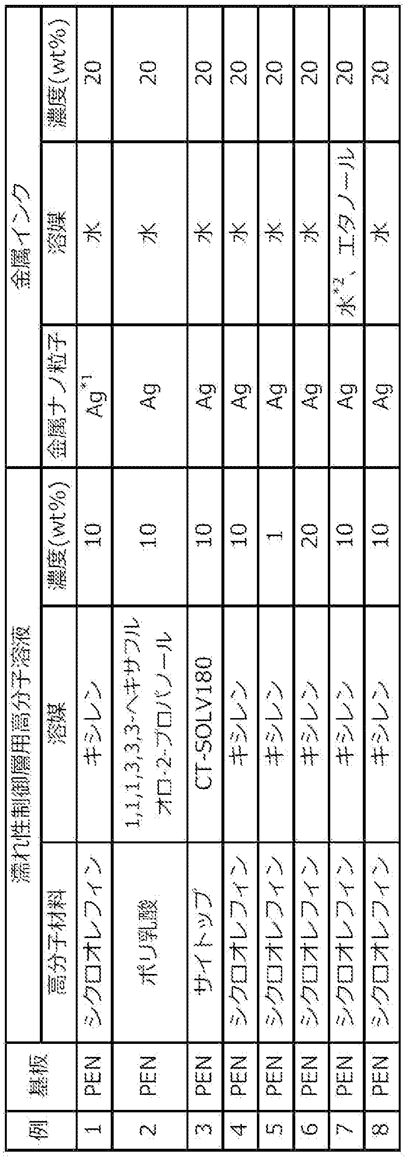
- Table 1 collectively shows the raw materials used in Examples 1 to 8.
- polymeric materials Sikuguchi olefin (manufactured by Zeon Corporation, Zeonex), polylactic acid (manufactured by Sigma-Aldrich, model number 7 6 7 3 4 4), Cytop (registered trademark) (manufactured by 8000, ⁇ Cho!_ — 8 0 9 1 ⁇ /1, and 0 0 1 30 [-V 180] was used as a diluting solvent.
- xylene manufactured by Wako Pure Chemical Industries
- 1, 1, 1, 1, 3, 3, 3, 3-hexafluoro-2-propanol manufactured by Sigma-Aldrich, model number 10 5 2 28
- ethanol manufactured by Wako Pure Chemical Industries
- Cytop has a structure different from that of cycloolefin polymer and polylactic acid.
- An ink containing metal nanoparticles was synthesized with reference to Non-Patent Document 2.
- It was modified to full Taroshianin as ligands in silver (eight 9) particles having a. It was prepared by using water so that the concentrations shown in Table 1 and ethanol were used if necessary.
- the substrate is polyethylene naphthalate (Min 1 ⁇ 1, manufactured by Teijin DuPont, Was used.
- Yuka (Mikasa,! ⁇ /!3100) was used to form the wettability control layer at the number of revolutions of 200 to 300", and then the wettability control layer was formed.
- the solvent was removed under the conditions shown below, and the thickness of the wettability control layer thus obtained was measured by a fine shape measuring instrument (Kosaka Laboratory, Model No. 200).
- the contact angle when anisole, which is a typical organic solvent, that the obtained wettability control layer satisfies hydrophobicity and lipophilicity was dropped was measured and confirmed, and the results are shown in Table 2.
- Cytop (registered trademark), which is a fluorine-based resin, does not satisfy the hydrophobic and lipophilic conditions as described in the detailed description of the present application.
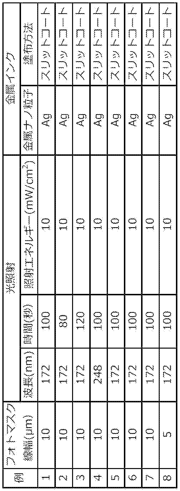
- a photomask having a line width of 10 or 5 was placed on the wettability control layers obtained in Examples 1 to 3 and Examples 5 to 8, and wavelengths of 20 It was irradiated with vacuum ultraviolet rays of 0 1 ⁇ or less (step 3120 in Fig. 1).
- the photomask having a line width of 10 further had 20 openings in the shape of a rectangular electrode pad at 100 1 intervals at the openings having a line width of 10.
- a xenon excimer lamp manufactured by Ushio, II II 1 ⁇ /1 2 0 _ 1 7 2 that emits a wavelength of 17 2 n was used for vacuum ultraviolet rays.
- the irradiation conditions are shown in Table 3. On the wettability control layer obtained in Example 4, a wavelength of 2 48 n is emitted. "I radiated an excimer laser.
- metal ink was applied onto the wettability control layer of Examples 1 to 8 irradiated with vacuum ultraviolet rays (step 3130 in Fig. 1).
- the metal ink was applied by the slit coating method.
- a slit coat type coating device Mitsubishi Chemical Vapor Company (3 _ 3)
- apply the coating speed was applied under the conditions.
- Fig. 5 is an optical microscope image showing the metal wiring of Example 1.
- FIG. 6 is an optical microscope image showing the metal wiring of Example 2.
- the bright lines in gray scale represent the metal wiring.
- the metal wiring in Examples 1 and 2 is ⁇ 2020/175 170 23 ⁇ (:171? 2020/005689
- the metal wirings of Examples 5 and 6 similarly had the line width of the photomask. From this, the thickness of the wettability control layer does not significantly affect the effect of the present invention, and the wettability control layer can be applied to 10 n or more and 100 or less, preferably 100 n or more. It was shown that a value of 10 or less is sufficient. Furthermore, in Example 6, when the wettability control layer was peeled from the Tami 1 ⁇ 1 substrate, it was found to function as a film-shaped two-dimensional metal wiring.
- Example 7 also had the line width of the photomask, but as compared with Examples 1 and 2, there were places where the boundary between the metal wiring and other portions was not clear. It was From this, it was shown that the solvent of the metal ink preferably contains 80% by volume or more of water.
- the metal wiring of Example 8 also had the line width (5) of the photomask. From this, it was confirmed that by using the method of the present invention, it is possible to easily form a metal thin wire having a line width of 10 or less, and further less than 10.
- the line width of the metal wiring (not shown) of Example 3 did not reach 10. From this, it was shown that the fluoropolymer does not function well as the wettability control layer.
- the line width of the metal wiring (not shown) in Example 4 was over 10. From this, it was shown that vacuum ultraviolet rays having a wavelength of 200 n or less are preferable for controlling the wettability of the wettability control layer made of the polymer material used in the present invention.
- the width of the metal wiring is the same as the width of the mask, and the boundary between the mouth and the metal wiring is very clear.
- the line width of the metal wiring exceeds the width of the mask (, ⁇ / reaches the width of the mask and does not exist.
- Example 9 to Example 10 three-dimensional metal wiring was formed using the two-dimensional metal wiring obtained in Example 1 to Example 2.
- the polymer solution was applied under the conditions of Table 1 and Table 2 to form a further wettability control layer.
- Step 3 3 10 in Figure 3 a recess was formed in the electrode pad shown in FIGS. 5 and 6 to expose the metal wiring (step 3320 in FIG. 3).
- the concave portion was formed by irradiating an ultraviolet ray laser with a wavelength of 2 66 11 01 (manufactured by Buoy Technology, model number V I--0 30).
- an organic semiconductor was prepared by the coating method using anisole as the organic solvent on the metal wiring of Example 3. The solution of pentacene was applied, but the organic semiconductor solution was not uniformly applied, and the organic semiconductor layer could not be formed. On the other hand, when an organic semiconductor was similarly applied to the metal wirings of Example 1 and Example 2, a uniform organic semiconductor layer could be formed. From this, it was shown that a wettability control layer having hydrophobicity and lipophilicity is important for forming an element such as an organic transistor.
- Example 11 polysilazane was used as the polymer material, a wettability control layer was formed on the substrate, and its characteristics were evaluated.
- polysilazane perhydropolysilazane Electronic Materials Co., Ltd., 8 1 2 0-2 0-8) was used. Butyl ether (diether Butyl ether) to prepare a polymer solution for the wettability control layer by adjusting the concentration of 1 to 13 to be 201%. Using this polymer solution, a wettability control layer was applied to the same substrate as in Examples 1 to 8 (manufactured by Teijin DuPont Co., Ltd., thickness 125, size 4 x 40) by spin coating. Formed (step 3 110 in Figure 1). For more information, visit Spinco ⁇ 2020/175 170 26 ⁇ (:171? 2020 /005689
- FIG. 7 shows Example 1 It is a spectrum.
- the thickness of the thus-obtained 3 x 2 film was measured by a fine shape measuring instrument (manufactured by Kosaka Laboratory, model number: 200) and was found to be 0.4 (400 nm). Further, the contact angle 0 at the time of dropwise anisole 3 ⁇ 2 film obtained is 0 °, the contact angle 0 when water was added dropwise was 90 °.
- Fig. 8 shows the measurement results of the light transmittance of the wettability control layer (Example 2 ) film. ⁇ 2020/175 170 27 ⁇ (:171? 2020/005689
- FIG. 8 3 ⁇ 2 film obtained in Example 1 1, be used as a material for a very high transparency as comparable to glass, to produce a transparent device It turned out to be fully expected.
- FIG. 9 is a eight IV! Image of Example 1 1 of the wettability control layer (3 ⁇ 2 film).
- FIG. 1 0 (3) is a Ding, M. IV! Image of wettability control layer formed on a 3 ⁇ wafer (3 ⁇ 2 film).
- Figure 10 (13) is the 3H8B pattern obtained for two regions in the same field of view as in Figure 10 (8).
- Example 1 1 obtained in wettability control layer (3 ⁇ 2 film), any of the case of using only and 3 ⁇ wafer substrate was subjected to drying treatment at lower than conventional methods temperature It is a thing. Therefore, according to the method of the present invention, the wettability control layer can be easily formed on a substrate such as a plastic which is likely to be thermally deformed under high temperature conditions. This is also costly.
- Example 12 polysilazane was used as the polymer material, and the wettability control layer was formed on various substrates by the spin coating method in the same procedure as in Example 11.
- the substrates used in Examples 12 to 15 were glass, cellulose nanovapor, 3 wafers, and Mitsumi, respectively.
- the glass and 3 I wafer were ultrasonically cleaned for 5 minutes each in the order of acetone, isopropanol, and distilled water before the polymer solution was applied by the spin coating method.
- Table 5 shows the materials and sizes of the substrates used in Examples 11 to 15.
- Table 5 A list of handwoven fabrics and properties for forming wettability control layers of Examples 11 to 15
- Example 1 2 With the formed on a smooth glass substrate wettability control layer I ⁇ 2 film), it was confirmed root mean square roughness is 0. 2 1 n.
- Example 1 In 3 on rough cellulose nano base supermarkets of the surface, the wettability control layer (3 I ⁇ 2 film) that is well formed, and root-mean-square roughness of the resultant 3 ⁇ 2 film was confirmed.
- a wettability control layer can be formed using a wide variety of materials as substrates, regardless of whether they are organic materials or inorganic materials, and a large area Can be applied to.
- Example 16 polysilazane was used as the polymer material, and the step of forming the wettability control layer by the spin coating method was repeated three times in the same procedure as in Example 11 so that the three-layer structure was formed on the M! A wettability control layer was formed.
- Figure 1 2 is a schematic drawing illustrating the analytic results of scanning white light interference microscope equipment of the wettability control layer Example 1 6 (3 I ⁇ 2 film).
- the spin coater rotation speed that is, the speed of the spin coating is changed to form the film on the substrate.
- the thickness of the wettability control layer is (S i ⁇ 2 film) can be controlled in the order of nanometers.
- this is also successful in the theoretical relational expression expressed by using the concentration of the polymer material in the polymer solution and the rotation speed of the spin coater, and the result of the preliminary experiment separately conducted by the inventors. Match.
- glass, silicon, nanovapor, or polymer can be used under lower temperature conditions. It is possible to easily form an extremely smooth S i O 2 film by using various materials such as the above as a substrate, and thereby the surface of the substrate material can be modified. In particular, it can be formed by layer by layer wettability control layer of the multilayer structure in a manner (Layer-by-Layer fashion) which are stacked in this order (S i ⁇ 2 film) solution process, advantageous to form a three-dimensional metal wire Is.
- Example 1 7 with Example 1 1 obtained in wettability control layer (S i ⁇ 2 film) was formed a two-dimensional metal wire.
- a photomask having a line width of 1 Ogm was placed on the wettability control layer (Si 0 2 film) obtained in Example 11 and irradiated with vacuum ultraviolet rays having a wavelength of 200 nm or less ( Step S120 of Figure 1).
- the photomask with the structure has a structure in which an opening having a line width of 10 Mm extends in one direction, is folded back by 180 ° at the end and extends in the opposite direction, and is further folded back by 180 ° at the opposite end.
- the opening had a continuous structure (pattern) as a whole.
- a xenon excimer lamp (Ushio Denki, U EM20-172) that emits a wavelength of 172 nm was used, and the irradiation time was 80 seconds. ⁇ 2020/175 170 32 ⁇ (:171? 2020 /005689
- Inks containing metal nanoparticles were synthesized with reference to Non-Patent Documents 2 and 3. Specifically, gold particles having a diameter of about 30 nm were prepared with water to a concentration of 25 I %. The metal ink was applied by the slit coating method. Using a slit coat type coating device (Mitsui Denki Seiki, Ding (3 _ 3), apply a coating speed of 5 Was applied under the conditions
- the state of the obtained metal wiring was observed with an optical microscope (manufactured by Nikon).
- FIG. 13 is an optical microscope image showing the metal wiring of Example 17.
- Fig. 13 bright lines (patterns) shown in gray scale represent metal wiring.
- the metal wiring of Example 17 has the line width (10) of the photomask, and the wiring/ ⁇ turn is obtained in which the structure of the opening of the photomask is reflected with high accuracy. I understood that it was done.
- Example 1 8 using a wettability control layer obtained in Example 1 1 (3 I ⁇ 2 film) was formed a three-dimensional metal wire.
- a rectangular electrode pad-shaped opening of 2 0 is further provided at an interval of 100 at an opening having a line width of 10. the same procedure as example 1 7 except for using things, to form a two-dimensional metal wiring on the wettability control layer (3 ⁇ 2 film).
- the polymer solution was applied under the same conditions as Example 1 1, further wettability control thereby forming a layer (3 ⁇ 2 film) (step 3 3 1 0 in FIG. 3).
- a recess was formed in the electrode pad to expose the metal wiring (step 3320 in FIG. 3).
- the concave portion was formed by irradiating an ultraviolet ray laser with a wavelength of 2666 n (manufactured by Buit Technology Co., Ltd., model number 1_-030).
- a photomask having a pad-shaped opening was placed, and vacuum ultraviolet rays of 200 n or less were irradiated under the same conditions as in Example 17 (step 3330 of FIG. 3). At this time, the photomask was arranged with its direction changed by 90 ° from that when the first-layer metal wiring was formed. Then, examples under the same conditions as 1 7, vacuum ultraviolet rays and the metallic ink is applied to a further wettability control layer (3 ⁇ 2 film) and recesses irradiated (Step 3 3 4 0 in FIG. 3). In this way, a three-dimensional metal wiring having a two-layer structure was formed.
- FIG. 14 ( 3 ) is an optical microscope image showing the metal wiring of Example 18.
- Fig. 14 ( 3 ) is an optical microscope image showing the metal wiring of Example 18.
- Figure 13 is an enlarged image of the part surrounded by the dotted line in Figure 14 (a).
- Fig. 14 ( ⁇ ) is a schematic diagram showing the structure of the portion shown in Fig. 14 ( ⁇ ).
- Fig. 14 (a) the bright lines in gray scale represent the metal wiring.
- the metal wiring of Example 18 had a line width (10) of the photomask.
- the part surrounded by the dotted line in Fig. 14 (a) one of the rectangular areas that exceeds the line width of the metal wiring is enlarged, and as shown in Fig. 14 ( ⁇ ) It was found that a three-dimensional metal wiring was obtained in which the metal wiring was bonded with the electrode pad. This is schematically shown in Fig. 14 ( ⁇ ).
Landscapes
- Engineering & Computer Science (AREA)
- Manufacturing & Machinery (AREA)
- Microelectronics & Electronic Packaging (AREA)
- Manufacturing Of Printed Wiring (AREA)
- Electrodes Of Semiconductors (AREA)
- Internal Circuitry In Semiconductor Integrated Circuit Devices (AREA)
Abstract
Description









Claims


Priority Applications (3)
| Application Number | Priority Date | Filing Date | Title |
|---|---|---|---|
| JP2021501926A JP7117047B2 (ja) | 2019-02-27 | 2020-02-14 | 金属配線を形成する方法 |
| KR1020217019793A KR102629707B1 (ko) | 2019-02-27 | 2020-02-14 | 금속 배선을 형성하는 방법 |
| CN202080015760.3A CN113454757A (zh) | 2019-02-27 | 2020-02-14 | 形成金属布线的方法 |
Applications Claiming Priority (2)
| Application Number | Priority Date | Filing Date | Title |
|---|---|---|---|
| JP2019-034506 | 2019-02-27 | ||
| JP2019034506 | 2019-02-27 |
Publications (1)
| Publication Number | Publication Date |
|---|---|
| WO2020175170A1 true WO2020175170A1 (ja) | 2020-09-03 |
Family
ID=72238278
Family Applications (1)
| Application Number | Title | Priority Date | Filing Date |
|---|---|---|---|
| PCT/JP2020/005689 Ceased WO2020175170A1 (ja) | 2019-02-27 | 2020-02-14 | 金属配線を形成する方法 |
Country Status (4)
| Country | Link |
|---|---|
| JP (1) | JP7117047B2 (ja) |
| KR (1) | KR102629707B1 (ja) |
| CN (1) | CN113454757A (ja) |
| WO (1) | WO2020175170A1 (ja) |
Cited By (1)
| Publication number | Priority date | Publication date | Assignee | Title |
|---|---|---|---|---|
| JP2024073157A (ja) * | 2022-11-17 | 2024-05-29 | 本田技研工業株式会社 | 導電層形成方法、および導電層形成装置 |
Citations (5)
| Publication number | Priority date | Publication date | Assignee | Title |
|---|---|---|---|---|
| JP2006108506A (ja) * | 2004-10-07 | 2006-04-20 | Seiko Epson Corp | 膜パターンの形成方法及び基板の製造方法 |
| JP2007150258A (ja) * | 2005-10-27 | 2007-06-14 | Seiko Epson Corp | パターン形成方法、膜構造体、電気光学装置及び電子機器 |
| JP2007300012A (ja) * | 2006-05-02 | 2007-11-15 | Seiko Epson Corp | 金属配線形成方法、アクティブマトリクス基板の製造方法、デバイス及び電気光学装置並びに電子機器 |
| WO2009044659A1 (ja) * | 2007-10-05 | 2009-04-09 | Konica Minolta Holdings, Inc. | パターン形成方法 |
| JP2013214649A (ja) * | 2012-04-03 | 2013-10-17 | Asahi Glass Co Ltd | 半導体装置およびその製造方法 |
Family Cites Families (2)
| Publication number | Priority date | Publication date | Assignee | Title |
|---|---|---|---|---|
| CN101189923B (zh) * | 2005-05-20 | 2010-10-06 | 富士胶片株式会社 | 图案形成方法及多层布线结构形成方法 |
| JP6197418B2 (ja) | 2013-07-05 | 2017-09-20 | 株式会社リコー | 積層配線の形成方法、積層配線、及び電子素子 |
-
2020
- 2020-02-14 WO PCT/JP2020/005689 patent/WO2020175170A1/ja not_active Ceased
- 2020-02-14 JP JP2021501926A patent/JP7117047B2/ja active Active
- 2020-02-14 CN CN202080015760.3A patent/CN113454757A/zh active Pending
- 2020-02-14 KR KR1020217019793A patent/KR102629707B1/ko active Active
Patent Citations (5)
| Publication number | Priority date | Publication date | Assignee | Title |
|---|---|---|---|---|
| JP2006108506A (ja) * | 2004-10-07 | 2006-04-20 | Seiko Epson Corp | 膜パターンの形成方法及び基板の製造方法 |
| JP2007150258A (ja) * | 2005-10-27 | 2007-06-14 | Seiko Epson Corp | パターン形成方法、膜構造体、電気光学装置及び電子機器 |
| JP2007300012A (ja) * | 2006-05-02 | 2007-11-15 | Seiko Epson Corp | 金属配線形成方法、アクティブマトリクス基板の製造方法、デバイス及び電気光学装置並びに電子機器 |
| WO2009044659A1 (ja) * | 2007-10-05 | 2009-04-09 | Konica Minolta Holdings, Inc. | パターン形成方法 |
| JP2013214649A (ja) * | 2012-04-03 | 2013-10-17 | Asahi Glass Co Ltd | 半導体装置およびその製造方法 |
Cited By (2)
| Publication number | Priority date | Publication date | Assignee | Title |
|---|---|---|---|---|
| JP2024073157A (ja) * | 2022-11-17 | 2024-05-29 | 本田技研工業株式会社 | 導電層形成方法、および導電層形成装置 |
| JP7881122B2 (ja) | 2022-11-17 | 2026-06-29 | 本田技研工業株式会社 | 導電層形成方法、および導電層形成装置 |
Also Published As
| Publication number | Publication date |
|---|---|
| KR20210100125A (ko) | 2021-08-13 |
| CN113454757A (zh) | 2021-09-28 |
| KR102629707B1 (ko) | 2024-01-29 |
| JP7117047B2 (ja) | 2022-08-12 |
| JPWO2020175170A1 (ja) | 2021-09-30 |
Similar Documents
| Publication | Publication Date | Title |
|---|---|---|
| JP7267624B2 (ja) | 複雑な金属酸化物構造のパターン形成 | |
| JP6366577B2 (ja) | 導電パターンの製造方法及び導電パターン形成基板 | |
| US20160205775A1 (en) | Transparent electrode and method for producing same | |
| TW200908024A (en) | Transparent conductive materials and coatings, methods of production and uses thereof | |
| CN104246974B (zh) | 利用激光蚀刻的图案形成方法 | |
| CN104735917B (zh) | 一种柱状嵌入式柔性电路的制备方法及应用 | |
| WO2008018392A1 (fr) | PROCÉDÉ DE FABRICATION DE composant de circuit électronique | |
| TWI719032B (zh) | 用於在製造一多層可印刷電子裝置對準金屬層之方法 | |
| TW201521984A (zh) | 使用熱層壓轉移來製造掩埋式可撓性電極膜之方法 | |
| CN1671805A (zh) | 烧结温度低的导电纳米油墨及其制备方法 | |
| CN102365713A (zh) | 增强光和/或激光烧结的缓冲层 | |
| JP2007182547A (ja) | 高導電性インク組成物および金属導電パターンの作製方法 | |
| Kirikova et al. | Direct-write printing of reactive oligomeric alkoxysilanes as an affordable and highly efficient route for promoting local adhesion of silver inks on polymer substrates | |
| JP2016110691A (ja) | 導電性基板の製造方法、及び導電性基板 | |
| EP2245212A2 (en) | Process for manufacturing conductive tracks | |
| Zhu et al. | Additive preparation of conductive circuit based on template transfer process using a reusable photoresist | |
| JP7117047B2 (ja) | 金属配線を形成する方法 | |
| Aminuzzaman et al. | Fabrication of conductive silver micropatterns on an organic–inorganic hybrid film by laser direct writing | |
| Tsujioka et al. | Selective noble-metal deposition modulation on photocurable polydimethylsiloxane films for electronics device applications | |
| CN107835974B (zh) | 包括通孔的电子设备以及形成此类电子设备的方法 | |
| Dawaymeh et al. | Exploring cyclic olefin copolymer (COC) for flexible silver nanowire electrode | |
| TW201601250A (zh) | 配線形成方法 | |
| Oh et al. | Selective multi-nanosoldering for fabrication of advanced solution-processed micro/nanoscale metal grid structures | |
| JP2018181677A (ja) | 透明導電配線パターン、透明導電配線基板及びその製造方法 | |
| TWI747607B (zh) | 形成絕緣層的墨水組成物、方法和觸控面板 |
Legal Events
| Date | Code | Title | Description |
|---|---|---|---|
| 121 | Ep: the epo has been informed by wipo that ep was designated in this application |
Ref document number: 20762312 Country of ref document: EP Kind code of ref document: A1 |
|
| ENP | Entry into the national phase |
Ref document number: 2021501926 Country of ref document: JP Kind code of ref document: A |
|
| ENP | Entry into the national phase |
Ref document number: 20217019793 Country of ref document: KR Kind code of ref document: A |
|
| NENP | Non-entry into the national phase |
Ref country code: DE |
|
| 122 | Ep: pct application non-entry in european phase |
Ref document number: 20762312 Country of ref document: EP Kind code of ref document: A1 |