WO2020170825A1 - トレンチキャパシタ及びトレンチキャパシタの製造方法 - Google Patents
トレンチキャパシタ及びトレンチキャパシタの製造方法 Download PDFInfo
- Publication number
- WO2020170825A1 WO2020170825A1 PCT/JP2020/004396 JP2020004396W WO2020170825A1 WO 2020170825 A1 WO2020170825 A1 WO 2020170825A1 JP 2020004396 W JP2020004396 W JP 2020004396W WO 2020170825 A1 WO2020170825 A1 WO 2020170825A1
- Authority
- WO
- WIPO (PCT)
- Prior art keywords
- trench
- wafer
- trench capacitor
- capacitor
- conductive layer
- Prior art date
- Legal status (The legal status is an assumption and is not a legal conclusion. Google has not performed a legal analysis and makes no representation as to the accuracy of the status listed.)
- Ceased
Links
Images






Classifications
-
- H—ELECTRICITY
- H01—ELECTRIC ELEMENTS
- H01G—CAPACITORS; CAPACITORS, RECTIFIERS, DETECTORS, SWITCHING DEVICES, LIGHT-SENSITIVE OR TEMPERATURE-SENSITIVE DEVICES OF THE ELECTROLYTIC TYPE
- H01G4/00—Fixed capacitors; Processes of their manufacture
- H01G4/30—Stacked capacitors
-
- H—ELECTRICITY
- H01—ELECTRIC ELEMENTS
- H01G—CAPACITORS; CAPACITORS, RECTIFIERS, DETECTORS, SWITCHING DEVICES, LIGHT-SENSITIVE OR TEMPERATURE-SENSITIVE DEVICES OF THE ELECTROLYTIC TYPE
- H01G4/00—Fixed capacitors; Processes of their manufacture
- H01G4/33—Thin- or thick-film capacitors (thin- or thick-film circuits; capacitors without a potential-jump or surface barrier specially adapted for integrated circuits, details thereof, multistep manufacturing processes therefor)
Definitions
- the present invention relates to a trench capacitor and a method for manufacturing the trench capacitor.
- a thin film capacitor that includes an MIM structure formed by a thin film process and that generates a capacitance by this MIM structure is known.
- the thin film capacitor it is required to improve the generated capacity per unit area in order to reduce the size and increase the capacity.
- a trench capacitor is known as a thin film capacitor that can improve the generated capacity per unit area.
- the trench capacitor includes a base material on which a large number of concave-convex structures called trenches are formed, and an MIM structure provided such that a part of the base material extends along the trench.
- the MIM structure is provided also in the trench extending in the thickness direction of the base material, so that the capacitance per unit area can be improved.
- Conventional trench capacitors are disclosed in Patent Documents 1 and 2, for example.
- a plurality of trench capacitors are formed on a single substrate, and then the substrate is cut by dicing to obtain individual trench capacitors.
- the trench capacitors may be damaged due to cutting by the dicing blade.
- An object of the present invention is to provide a trench capacitor in which damage due to cutting is suppressed and a method for manufacturing the trench capacitor.
- a trench capacitor according to one embodiment of the present invention has an upper surface, a lower surface opposite to the upper surface, a side surface connecting the upper surface and the lower surface, and a trench provided with a trench extending from the upper surface in the vertical direction. And a first conductive layer, a second conductive layer, and a dielectric layer sandwiched between the first conductive layer and the second conductive layer, and provided along the wall surface defining the upper surface and the trench. And a plurality of side surface scallops from the upper end to the lower end of the side surface of the base material.
- a plurality of scallops are formed side by side from the upper end to the lower end of the side surface on at least a part of the side surface of the base material of this trench capacitor.
- the side surface scallops formed by etching using the Bosch process are formed on the side surfaces of the base material, the trench capacitors are singulated by etching. Therefore, damage to the trench capacitor due to cutting by the dicing blade can be suppressed.
- a plurality of sidewall scallops are formed from an upper end to a lower end of a sidewall that defines a trench and extends in the up-down direction.
- the n-th sidewall scallop from the upper side is formed.
- the shape of the nth side face scallop from the upper side among the plurality of side face scallops may be similar.
- the manufacturing process of the trench capacitor can be simplified. Therefore, the trench capacitor can be easily manufactured.
- the base material may be L-shaped, T-shaped, cross-shaped, or circular when viewed from above and below.
- the trench capacitor according to the embodiment of the present invention is singulated by etching, it is possible to singulate the trench capacitor into a shape other than the rectangular shape. Therefore, by using the trench capacitor, the degree of freedom in designing a circuit board or the like can be improved.
- One embodiment of the present invention relates to a circuit board including any one of the above trench capacitors.
- One embodiment of the present invention relates to an electronic device including the above circuit board.
- a method for manufacturing a trench capacitor according to an embodiment of the present invention is a method for manufacturing a plurality of trench capacitors by dividing a wafer having an upper surface and a lower surface opposite to the upper surface into individual wafers.
- a MIM structure having a second step, a first conductive layer, a second conductive layer, and a dielectric layer sandwiched between the first conductive layer and the second conductive layer is formed on a wall surface and an upper surface defining a trench. It includes a third step of providing the wafer along with a fourth step of thinning the wafer from the lower surface side to divide the wafer into individual pieces.
- the trench capacitors are separated into individual pieces without using dicing, so that damage to the trench capacitors due to cutting with a dicing blade can be suppressed. Further, in the method of manufacturing the trench capacitor, the boundary groove and the trench for separating the plurality of trench capacitors are formed by the same etching process, so that the manufacturing process of the trench capacitor can be simplified. Therefore, the trench capacitor can be easily manufactured.
- the wafer in the second step, may be etched using a Bosch process, and the trench and the boundary groove may be formed by utilizing a microloading effect.
- the wafer may be diced by performing etching and grinding in the fourth step.
- the lower surface of the base material of the trench capacitor can be made smoother than in the case where the wafer is singulated only by grinding.
- the thickness of the wafer to be removed can be controlled with high accuracy as compared with the case where the wafer is singulated only by grinding.
- the wafer may be diced by grinding in the fourth step. According to this configuration, the processing time of the fourth step can be shortened as compared with the case where the wafer is divided into individual pieces by etching.
- a trench capacitor and a method of manufacturing the trench capacitor capable of improving the yield.
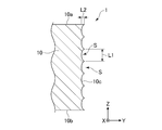
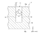
- FIG. 2 is a cross-sectional view schematically showing a cross section of the trench capacitor of FIG. 1 taken along the line II. It is sectional drawing which expands and shows the trench part of the trench capacitor of FIG. It is sectional drawing which shows the shape of the side surface of a base material roughly. It is sectional drawing which shows roughly the shape of the side wall which defines a trench.
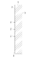
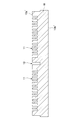
- FIG. 6 is a diagram for explaining a manufacturing process of the trench capacitor of FIG. 1.
- FIG. 6 is a diagram for explaining a manufacturing process of the trench capacitor of FIG. 1.
- FIG. 6 is a diagram for explaining a manufacturing process of the trench capacitor of FIG. 1.
- FIG. 6 is a diagram for explaining a manufacturing process of the trench capacitor of FIG. 1.
- FIG. 6 is a diagram for explaining a manufacturing process of the trench capacitor of FIG.
- FIG. 6 is a diagram for explaining a manufacturing process of the trench capacitor of FIG. 1.
- FIG. 6 is a diagram for explaining a manufacturing process of the trench capacitor of FIG. 1.
- FIG. 6 is a diagram for explaining a manufacturing process of the trench capacitor of FIG. 1.
- FIG. 6 is a diagram for explaining a manufacturing process of the trench capacitor of FIG. 1.
- FIG. 6 is a diagram for explaining a manufacturing process of the trench capacitor of FIG. 1.
- FIG. 6 is a diagram for explaining a manufacturing process of the trench capacitor of FIG. 1.
- FIG. 1 is a schematic plan view of the trench capacitor 1
- FIG. 2 is a sectional view schematically showing a cross section of the trench capacitor 1 taken along the line II.
- FIG. 3 is an enlarged sectional view showing a trench portion of the trench capacitor.
- the trench capacitor 1 includes a base material 10, an MIM structure 20 provided on the base material 10, and a protective layer 40 provided so as to cover the MIM structure 20. ..
- the outer electrode 2 and the outer electrode 3 are provided outside the protective layer 40.
- the external electrodes 2 and 3 are electrically connected to the electrode layers forming the MIM structure 20, as will be described later in detail.
- the trench capacitor 1 is mounted on the circuit board by bonding the external electrode 2 and the external electrode 3 to a land provided on the circuit board.
- This circuit board can be mounted on various electronic devices.
- the electronic device including the circuit board on which the trench capacitor 1 is mounted includes a smart phone, a mobile phone, a tablet terminal, a game console, and any other electronic device that can include a circuit board on which the trench capacitor 1 is mounted. included.
- the X direction, the Y direction, and the Z direction that are orthogonal to each other are shown.
- the directions and arrangements of the constituent members of the trench capacitor 1 may be described with reference to the X direction, the Y direction, and the Z direction shown in these drawings.
- the “width” direction, the “length” direction, and the “thickness” direction of the thin film capacitor 1 are respectively the directions along the X axis and the Y axis of FIG.
- the direction along the Z-axis when referring to the vertical direction of the trench capacitor 1 and its constituent members, the positive direction of the Z-axis is the upward direction of the trench capacitor 1 and the negative direction of the Z-axis, unless otherwise understood in the context.
- the direction is the downward direction of the trench capacitor 1.
- the base material 10 is made of an insulating material such as Si.
- the base material 10 is formed in a substantially rectangular parallelepiped shape, and the dimension in the width direction (X axis direction) is, for example, 50 ⁇ m to 5000 ⁇ m, and the dimension in the length direction (Y axis direction) is.
- the thickness is, for example, 50 ⁇ m to 5000 ⁇ m, and the dimension in the thickness direction (Z-axis direction) is, for example, 5 ⁇ m to 500 ⁇ m.
- the dimensions of the base material 10 specifically shown in the present specification are merely examples, and the base material 10 can have any dimensions.
- the base material 10 has an upper surface 10a, a lower surface 10b opposite to the upper surface 10a, and a side surface 10c connecting the upper surface 10a and the lower surface 10b.
- the base material 10 has a substantially rectangular parallelepiped shape, and in the present specification, the four surfaces that connect the upper surface 10a and the lower surface 10b of the base material 10 are collectively referred to as a side surface 10c.
- the base material 10 has a plurality of trenches 11 extending from the top surface 10a thereof along the Z-axis direction. Each of the plurality of trenches 11 is formed so as to have a predetermined depth in the Z-axis direction. In this specification, the Z-axis direction may be referred to as the depth direction of the trench 11.
- each of the plurality of trenches 11 has a substantially rectangular shape in plan view defined by a side extending along the X-axis direction and a side extending along the Y-axis direction. Is formed. In the illustrated embodiment, each of the plurality of trenches 11 is formed such that a side extending along the X-axis direction is shorter than a side extending along the Y-axis direction in a plan view.
- each of the plurality of trenches 11 is formed to have a high aspect ratio in order to realize a high capacity per unit area. That is, each of the plurality of trenches 11 is formed such that the ratio of the depth (dimension in the Z-axis direction) to the width (for example, the length of the side in the X-axis direction) is large.
- the width (dimension in the X-axis direction) of each of the plurality of trenches 11 is, for example, 0.1 ⁇ m to 5 ⁇ m, and the depth (dimension in the Z-axis direction) is, for example, 1 ⁇ m to 100 ⁇ m.
- the dimensions of the trench 11 specifically shown in the present specification are merely examples, and the trench 11 can have any dimensions.
- the shape of the trench 11 in plan view is not limited to the rectangular shape, and the trench 11 can have any shape.
- the trench 11 has a depth (dimension in the Z-axis direction) of 40 ⁇ m and a width (dimension in the X-axis direction) of 1.0 ⁇ m.
- the trench 11 can be formed, for example, by forming a mask having an opening corresponding to the pattern of the trench 11 on the surface of the Si substrate and then etching the Si substrate by etching.
- the etching process of the trench 11 may be performed by a reactive ion etching method such as deep RIE (deep reactive etching) using the Bosch process.
- Adjacent trenches 11 of the plurality of trenches 11 are separated by a sidewall 12.
- the sidewall 12 is part of the substrate 10 and is configured to separate adjacent trenches 11 from each other.
- the MIM structure 20 will be described. As described above, the MIM structure 20 is provided on the base material 10. As shown in the figure, the base material 10 is provided so that a part thereof is embedded in each of the trenches 11.
- the MIM structure 20 is configured to have a shape that follows the upper surface 10 a of the base material 10 and the trench 11.
- the MIM structure 20 has a first conductive layer, a second conductive layer, and a dielectric layer sandwiched between the first conductive layer and the second conductive layer. That is, the MIM structure 20 is a laminated body in which conductive layers and conductor layers are alternately laminated.
- the MIM structure 20 according to the embodiment is provided with a lower electrode layer 22 (first conductive layer), a dielectric layer 21 provided on the lower electrode layer 22, and a dielectric layer 21 provided on the dielectric layer 21. And an upper electrode layer 23 (second conductive layer).
- the base material 10 is not the vertical direction along the Z-axis direction but the vertical direction along the Z-axis direction in order to be consistent with the commonly used names of the lower electrode and the upper electrode.
- the side closer to is referred to as “lower”, and the side farther from the substrate 10 is referred to as “upper”.
- the MIM structure 20 may include two or more MIM layers.
- the second layer is formed on the first MIM layer composed of the lower electrode layer 22, the dielectric layer 21, and the upper electrode layer 23.
- the MIM layer of the eye is formed.
- the second MIM layer can include a dielectric layer provided on the upper electrode layer 23 and an electrode layer provided on the dielectric layer.
- the upper electrode layer 23 has both a function as an electrode layer above the first MIM layer and a function as an electrode layer below the second MIM layer.
- BST barium strontium titanate
- BTO barium titanate
- STO strontium titanate
- ZrO2 zirconia
- Al2O3 zirconia
- Al2O3 zirconia
- hafnium oxide hafO2
- TiO2 titanium oxide
- dielectric materials other than these can be used.
- the material of the dielectric layer 21 is not limited to those explicitly described herein.
- the dielectric layer 21 is formed by, for example, an ALD (atomic layer deposition) method, a sputtering method, a CVD method, a vapor deposition method, a plating method, or a known method other than these.
- the dielectric layer 21 is formed to have a film thickness of, for example, 1 nm to 500 nm. In one embodiment, the thickness of the dielectric layer 21 is 30 nm.
- Ni nickel (Ni), copper (Cu), palladium (Pd), platinum (Pt), silver (Ag), gold (Au), ruthenium (Ru), tungsten (W).
- Molybdenum (Mo) titanium (Ti), conductive silicon, or a metal material other than these, an alloy material containing one or more of these metal elements, and a compound of the metal element can be used.
- titanium nitride (TiN) is used as the material of the lower electrode layer 22 and the upper electrode layer 23.
- the materials of the lower electrode layer 22 and the upper electrode layer 23 are not limited to those explicitly described in this specification.
- the lower electrode layer 22 and the upper electrode layer 23 are formed by, for example, an ALD (atomic layer deposition) method, a sputtering method, a vapor deposition method, a plating method, or a known method other than these.
- the lower electrode layer 22 is formed to have a film thickness of, for example, 1 nm to 500 nm.
- the upper electrode 23 is formed to have a film thickness of, for example, 1 nm to 500 nm.
- the thicknesses of the lower electrode layer 22 and the upper electrode layer 23 are each 30 nm.
- the film thicknesses of the lower electrode layer 22 and the upper electrode layer 23 are each 30 nm.
- the film thicknesses of the lower electrode layer 22 and the upper electrode layer 23 are not limited to those explicitly described in this specification.
- the protective layer 40 is provided to cover the MIM structure 20 and the base material 10 in order to protect the MIM structure 20 from the external environment.
- the protective layer 40 is provided so as to protect the MIM structure 20 from mechanical damage such as impact from the outside.
- a resin material such as polyimide, silicon oxide (SiO2), silicon nitride (SiN), silicon oxynitride (SiON), or an insulating material other than these can be used.
- the protective layer 40 is formed, for example, by applying a photosensitive polyimide by a spin coating method and exposing, developing, and curing the applied polyimide.
- the protective layer 40 is formed to have a film thickness of, for example, 200 nm to 5000 nm. In one embodiment, the protective layer 40 has a thickness of 3000 nm. The material and film thickness of the protective layer 40 are not limited to those explicitly described in this specification.
- a barrier layer (not shown) may be provided between the protective layer 40 and the MIM structure 20 (or the base material 10).
- the barrier layer is provided mainly on the MIM structure 20 in order to improve the weather resistance of the trench capacitor 1.
- the barrier layer is provided between the MIM structure 20 and the protective layer 40 so that moisture released from the protective layer 40 or moisture in the atmosphere does not reach the MIM structure 20.
- the barrier layer may be a thin film having an excellent hydrogen gas barrier property.
- As the material of the barrier layer alumina (Al2O3), silicon oxide (SiO2), silicon oxynitride (SiON), zirconia (ZrO2), and other insulating materials can be used.
- the barrier layer is formed by, for example, a sputtering method, a CVD method, or a known method other than these.
- the barrier layer is formed to have a film thickness of, for example, 5 nm to 500 nm. In one embodiment, the barrier layer thickness is 50 nm.
- the barrier layer material and thickness are not limited to those explicitly described herein.
- the external electrodes 2 and 3 are provided on the upper side of the protective layer 40 so as to be separated from each other in the Y-axis direction.
- the external electrodes 2 and 3 are formed by applying a conductor paste containing a metal material to the outside of the protective layer 40.
- the material of the external electrodes 2 and 3 is copper (Cu), nickel (Ni), tin (Sn), palladium (Pd), platinum (Pt), silver (Ag), gold (Au), or other materials.
- a metal material or an alloy material containing one or more of these metal elements can be used.
- At least one of a solder barrier layer and a solder leak layer may be formed on the external electrode 2 and the external electrode 3 as necessary.
- a groove 41 is provided near the Y-axis negative direction end of the protective layer 40, and a groove 42 is provided near the Y-axis positive direction end thereof. Both the groove 41 and the groove 42 are provided so as to extend along the X-axis direction and penetrate the protective layer 40 in the Z-axis direction.
- the extraction electrode 2a is provided in the groove 41, and the extraction electrode 3a is provided in the groove 42.
- the upper end of the extraction electrode 2a is connected to the external electrode 2, and the lower end of the extraction electrode 2a is connected to the lower electrode layer 22 of the MIM structure 20.
- the upper end of the extraction electrode 3a is connected to the external electrode 3, and the lower end of the extraction electrode 3a is connected to the upper electrode 23 of the MIM structure 20.
- the material of the extraction electrodes 2a and 3a copper (Cu), nickel (Ni), tin (Sn), palladium (Pd), platinum (Pt), silver (Ag), gold (Au), or a metal material other than these Alternatively, an alloy material containing one or more of these metal elements can be used.
- the extraction electrodes 2a and 3a are formed by a vapor deposition method, a sputtering method, a plating method, or any other known method.
- FIG. 4a is a sectional view schematically showing the shape of the side surface 10c of the base material 10.
- FIG. 4 b is a cross-sectional view schematically showing the shape of the side wall 12 that defines the trench 11.
- a plurality of side surface scallops S are formed from the upper end to the lower end of the side surface 10c.
- the plurality of side surface scallops S are formed by etching using the Bosch process.
- a cycle including a step of etching the base material and a step of forming a protective film on the surface of the base material is continuously repeated a plurality of times. By carrying out such a cycle once, one scallop is formed. Therefore, the number of side surface scallops S formed on the side surface 10c corresponds to the number of etching cycles using the Bosch process.
- each side surface scallop S is a U-shaped groove that extends along a plane (that is, a plane along the X axis and the Y axis) that intersects with the thickness direction (that is, the Z axis direction) of the base material 10. That is, the side surface 10c is composed of a plurality of curved concave surfaces arranged along the Z-axis direction. In the embodiment of FIG.
- the side surface scallop S has a plurality of side surface scallops S formed from the upper end to the lower end on the entire surface of the side surface 10c (that is, the four surfaces connecting the upper surface 10a and the lower surface 10b of the base material 10). ing.
- FIG. 4a for convenience of explanation, an embodiment in which seven side surface scallops S are formed on the side surface 10c is shown, but in reality, a larger number of side surface scallops S may be formed on the side surface 10c.
- the number of scallops S formed on the side surface 10c is not particularly limited.
- the side face scallops S may be formed side by side from the upper end to the lower end only on a part of the side face 10c.
- each of the plurality of scallops S has substantially the same shape as each other.
- the dimension L1 of the scallop S in the Z-axis direction can be, for example, 1 nm or more and 500 nm or less.
- the dimension L2 of the scallop S in the direction intersecting the Z-axis direction can be, for example, 0.5 nm or more and 250 nm or less.
- the sidewall 12 defining the trench 11 is formed with a plurality of sidewall scallops S'.
- the side wall 12 is a wall surface that extends along the Z-axis direction among the wall surfaces that define the trench 11.
- the plurality of side wall scallops S′ are formed side by side from the upper end to the lower end of the side wall 12.
- Each side wall scallop S′ is a U-shaped groove extending along a direction (that is, the X-axis direction or the Y-axis direction) that intersects with the thickness direction (that is, the Z-axis direction) of the base material 10, similarly to the side-face scallop S. is there.
- the side wall 12 is composed of a plurality of curved concave surfaces arranged along the axial direction.
- FIG. 4 b for convenience of explanation, an embodiment is shown in which seven sidewall scallops S′ are formed on the sidewall 12.
- each of the plurality of sidewall scallops S' has a substantially identical shape.
- the dimension L1' of the sidewall scallop S'in the Z-axis direction can be, for example, 1 nm or more and 500 nm or less.
- the dimension L2' of the sidewall scallop S'in the direction intersecting the Z-axis direction can be set to, for example, 0.5 nm or more and 250 nm or less.
- the scallop provided on the side surface 10c of the base material 10 may be referred to as a "side surface scallop S".
- the side surface scallop S formed on the side surface 10c of the base material 10 and the side wall scallop S'formed on the side wall 12 are formed by the same etching process. Since the number of scallops is determined by the number of cycles in the Bosch process, the number of side face scallops S formed on the side face 10c and the number of side wall scallops S'formed on the side wall 12 are the same. In addition, in the manufacturing process of the trench capacitor 1, due to the difference between the area of the region to be the trench 12 (trench region described later) and the area of the region etched (boundary region described later) when the side surface 10c is formed, Due to the loading effect, the side face scallop S and the side wall scallop S′ have similar shapes.
- the side face scallop S and the side wall scallop S′ are similar to each other means that, if the shape of one scallop is enlarged or reduced evenly, it becomes the same as the shape of the other scallop.
- the ratio of the dimension L1′ of the side wall scallop S′ to the dimension L1 of the side surface scallop S and the ratio of the dimension L2′ of the side wall scallop S′ to the dimension L2 of the side surface scallop S are For example, it is 10% or more and 300% or less.
- similarity When the term “similarity” is used in this specification, it is not used in a mathematically strict sense, and a shape shift caused by a manufacturing error and/or a measurement error is allowed.
- the determination of “similarity” can be made by the following method, for example. First, an image of the cross-sectional shape of the side surface 10c corresponding to FIG. 4a and the cross-sectional shape of the side wall 12 corresponding to FIG. 4b are acquired using SEM or the like. Next, the cross-sectional shape of the sidewall 12 is uniformly enlarged so that the dimension of the sidewall 12 in the Z-axis direction (that is, the dimension from the upper end to the lower end of the sidewall 12) becomes the same as the dimension of the side surface 10c in the Z-axis direction.
- the upper and lower ends of the side surface 10c are arranged so as to overlap with the upper and lower ends of the side wall 12, respectively.
- the deviation between the dimension L1 of the side surface scallop S and the dimension L1′ of the side wall scallop S′ is about 1% to 30% of the dimension L1
- the dimension L2 of the side surface scallop S and the dimension L2′ of the side wall scallop S′ are If the deviation is about 1% to 30% of the dimension L2, it is regarded as “similar”.
- the shapes of the plurality of side surface scallops S are all substantially the same.
- the shapes of the plurality of side surface scallops S formed on the side surface 10c may not all be substantially the same.
- the shapes of the plurality of side wall scallops S'formed on the side wall 12 may not all be substantially the same.
- at least the shape of the sidewall scallop S′ located at the n-th (n is a natural number) from the upper side of the plurality of sidewall scallops S′ and the side-face scallop S located at the n-th side of the plurality of side-face scallops S. It suffices if it is similar to the shape of. That is, only the shape of the side surface scallop S and the shape of the side wall scallop S′ formed by the same cycle in the Bosch process need to be similar.
- FIGS. 5 and 6a to 6i are views for explaining a manufacturing process of the trench capacitor according to the embodiment.
- a wafer-shaped wafer W having an upper surface 10a' and a lower surface 10b' is prepared.
- a plurality of capacitor regions R1 in which the trench capacitors 1 are formed are adjacent to the upper surface 10a′ of the wafer W in the wafer shape and in the first direction along the upper surface 10a′.
- a mask M1 having a boundary region R13 located between the matching capacitor regions R1 and a trench region R11 provided in the capacitor region R1 and having a trench formed therein is formed (first step).
- the patterns of the plurality of trench regions R11 correspond to the positions of the plurality of trenches 11 shown in FIG.
- the boundary region R13 is a region located between the regions R1 in which the trench capacitors 1 are formed in the direction along the upper surface 10a'.
- the boundary region R13 becomes a rectangular region, and the short side of the boundary region R13 has a dimension of the adjacent regions R1 in the X-axis direction.
- the size of the long side of the boundary region R13 corresponds to the space between the two, and the size of the long side of the boundary region R13 corresponds to the size of the region R1 in the Y-axis direction.
- the dimension of the short side of the boundary region R13 corresponds to the interval between the regions R1 adjacent to each other in the Y-axis direction, and the length of the long side of the boundary region R13.
- the dimension corresponds to the dimension of the region R1 in the X-axis direction.
- FIG. 5 shows the boundary region R13 when the direction along the upper surface 10a is the X-axis direction.
- the size of the short side of the boundary region R13 can be about 1 ⁇ m to 100 ⁇ m
- the size of the long side of the boundary region R13 can be about 100 ⁇ m to 10 mm.
- the ratio of the area of the boundary region R13 to the area of one trench region R11 can be about 0.0001% to 10%.
- the trench 11 extending from the upper surface 10a′ along the Z-axis direction is formed in the trench region R11, and the boundary groove 13 is formed in the boundary region R13.
- the etching of the wafer W is performed by dry etching using, for example, the Bosch process. Since the boundary region R13 has a larger area than each trench region R11, the boundary groove 13 is etched deeper than the trench 11 due to the microloading effect.
- the Bosch process is used in this step, a plurality of sidewall scallops S′ are formed on the sidewall 12 that defines the trench 11.
- a plurality of side surface scallops S are formed on the side wall that defines the boundary groove 13 (that is, the wall surface that will be the side surface 10c later).
- the mask M1 is removed from the wafer-shaped wafer W (see FIG. 6c). Thereafter, as shown in FIG. 6d, an MIM structure 20 including a plurality of lower electrode layers 22, a dielectric layer 21, and an upper electrode layer 23 is formed inside the upper surface 10a′ of the wafer W and the trench 11. Third step).
- the MIM structure 20 is formed along the wall surface that defines the upper surface 10 a ′, the trench 11, and the boundary groove 13.
- the dielectric layer 21 may be formed of, for example, zirconia, and the lower electrode layer 22 and the upper electrode layer 23 may be formed of TiN.
- Each layer (that is, the lower electrode layer 22, the dielectric layer 21, and the upper electrode layer 23) included in the MIM structure 20 can be formed by the ALD method.
- the material of the dielectric layer 22 is not limited to zirconia, and the materials of the lower electrode layer 22 and the upper electrode layer 23 are not limited to TiN.
- the lower electrode layer 22, the dielectric layer 21, and the upper electrode layer 23 may be formed by various known methods other than the ALD method.
- a mask M2 that integrally covers the plurality of trenches 11 when viewed from the Z-axis direction is formed, and the MIM structure 20 is etched using this mask M2.
- the MIM structure 20 formed inside the boundary groove 13 is removed (see FIGS. 6e and 6f).
- a protective layer 40 is formed on the MIM structure 20.
- the grooves 41 and 42 are provided near each of both ends in the Y-axis direction of the portion of the protective layer 40 provided on the upper side of the MIM structure 20.
- the extraction electrodes 2a and 3a are formed inside the grooves 41 and 42 by a plating method or the like, and the external electrodes 2 and 3 are formed on the surface of the protective layer 40 (see FIG. 6g).
- the wafer W is thinned from the lower surface 10b' side to divide the wafer W into individual substrates 10 (fourth step).
- the thinning of the wafer W can be performed by removing a part of the lower surface 10b' of the wafer W by, for example, etching, grinding, or a method using etching and grinding in combination.
- the lower surface 10b of the base material 10 of the trench capacitor 1 is made smoother than when the wafer W is singulated by only grinding. You can In addition, the thickness of the wafer W to be removed can be controlled with high accuracy as compared with the case where the wafer W is singulated only by grinding. When the wafer W is singulated only by grinding, the processing time can be shortened as compared with the case where the wafer W is singulated by etching. Through the above steps, a plurality of trench capacitors 1 are obtained.
- the etching is performed at the timing when the position of the etching surface in the vertical direction coincides with the bottom surface of the boundary groove 13 (that is, the timing when the bottom surface of the boundary groove 13 is removed). Stop.
- the number of the side surface scallops S formed on the side surface 10c and the number of the side wall scallops S'formed on the side wall 12 are the same.
- the etching may be stopped at the timing when the position of the etching surface in the vertical direction exceeds the bottom surface of the boundary groove 13. In this case, the number of scallops S formed on the side surface 10c and the number of scallops S'formed on the side wall 12 may not be the same.
- a plurality of side surface scallops S are formed side by side from the upper end to the lower end of the side surface 10c on at least a part of the side surface 10c of the base material 10 of the trench capacitor 1.
- the side surface scallop S formed by the etching using the Bosch process is formed on the side surface 10c of the base material, the trench capacitor 1 is singulated by the etching. Therefore, damage to the trench capacitor 1 due to cutting by the dicing blade can be suppressed, and the yield can be improved.
- a plurality of side wall scallops S are arranged side by side from the upper end to the lower end of the side wall 12 defining the trench 11 and extending in the vertical direction, and the upper side of the plurality of side wall scallops S′ is formed.
- the shape of the side wall scallop S′ from the nth to the side is similar to the shape of the side surface scallop S from the upper side of the plurality of side surface scallops S.
- the manufacturing process of the trench capacitor 1 can be simplified. Therefore, the trench capacitor 1 can be easily manufactured.
- the trench capacitors 1 are separated into individual pieces by etching, so that the damage of the trench capacitors 1 due to the cutting by the dicing blade can be suppressed.
- the base material is etched by using the Bosch process to form the trench by utilizing the microloading effect, and the boundary groove deeper than the trench is formed. Since the boundary groove 13 and the trench 11 for separating the plurality of trench capacitors 1 can be formed in the same etching process as described above, the manufacturing process of the trench capacitor 1 can be simplified. Therefore, the trench capacitor 1 can be easily manufactured.
- the shape of the base material 10 is not limited to a rectangular shape when viewed from the Z-axis direction (that is, the vertical direction), and can be changed as appropriate.
- the base material 10 may have an L shape, a T shape, a cross shape, or a circular shape when viewed from the Z-axis direction.
- the trench capacitor 1 is singulated by etching, it is possible to singulate the trench capacitor 1 into a shape other than the rectangular shape. Therefore, by using the trench capacitor 1, the degree of freedom in designing a circuit board or the like can be improved.
- each component described herein is not limited to those explicitly described in the embodiments, and each component may be included in the scope of the present invention. Can be modified to have different dimensions, materials, and configurations.
- components that are not explicitly described in this specification may be added to the described embodiments, or some of the components described in each embodiment may be omitted.
- the one object when it is described that one object is provided “above”, “upper surface”, “below”, or “lower surface” of another object, the one object is referred to as the other object. It may be in direct contact, or may be in indirect contact via another layer or film.
- SYMBOLS 1 Trench capacitor, 10... Base material, 10a... Top surface, 10c... Side surface, 11... Trench, 12... Side wall, 13... Boundary groove, 20... MIM structure, R11... Trench region, R13... Boundary region, S... Side surface Scallop, S'... Sidewall scallop.
Landscapes
- Engineering & Computer Science (AREA)
- Power Engineering (AREA)
- Microelectronics & Electronic Packaging (AREA)
- Manufacturing & Machinery (AREA)
- Semiconductor Integrated Circuits (AREA)
- Ceramic Capacitors (AREA)
- Fixed Capacitors And Capacitor Manufacturing Machines (AREA)
Abstract
歩留まりの向上を図ることが可能なトレンチキャパシタ及びトレンチキャパシタの製造方法を提供する。トレンチキャパシタ1は、上面10aと、上面10aとは反対側の下面10bと、上面10a及び下面10bを接続する側面10cとを有し、上下方向に沿って上面10aから延びるトレンチ11が設けられた基材10と、下部電極層22と、上部電極層23と、下部電極層22と上部電極層23とに挟まれた誘電体層21とを有し、上面10a及びトレンチ11を画定する壁面に沿って設けられたMIM構造体20と、を備え、基材10の側面10cの上端から下端まで複数の側面スキャロップSが形成されている。
Description
相互参照
本出願は、日本国特許出願2019-027286(2019年2月19日出願)に基づく優先権を主張し、その内容は参照により全体として本明細書に組み込まれる。
本発明は、トレンチキャパシタ及びトレンチキャパシタの製造方法に関する。
本出願は、日本国特許出願2019-027286(2019年2月19日出願)に基づく優先権を主張し、その内容は参照により全体として本明細書に組み込まれる。
本発明は、トレンチキャパシタ及びトレンチキャパシタの製造方法に関する。
キャパシタの一種として、薄膜プロセスにより形成されたMIM構造体を備え、このMIM構造体により容量を発生させる薄膜キャパシタが知られている。薄膜キャパシタにおいては、小型化又は高容量化のために、単位面積あたりの発生容量を向上させることが求められている。
単位面積あたりの発生容量を向上させることが可能な薄膜キャパシタとして、トレンチキャパシタが知られている。トレンチキャパシタは、トレンチと呼ばれる凹凸構造が多数形成された基材と、その一部がトレンチに沿って延伸するように設けられたMIM構造体と、を備えている。トレンチキャパシタにおいては、基材の厚さ方向に延びるトレンチ内にもMIM構造体が設けられるため、単位面積当たりの容量を向上させることができる。従来のトレンチキャパシタは、例えば、特許文献1及び2に開示されている。
従来の製造工程においては、一枚の基板上に複数のトレンチキャパシタを形成し、その後、ダイシングによって当該基板を切削することで、個片化されたトレンチキャパシタが得られる。しかしながら、ダイシングによって個片化を行う場合、ダイシングブレードによる切削に起因して、トレンチキャパシタが破損する可能性がある。
本発明は、切削による破損が抑制されたトレンチキャパシタ及びトレンチキャパシタの製造方法を提供することを目的とする。
本発明の一実施形態に係るトレンチキャパシタは、上面と、上面とは反対側の下面と、上面及び下面を接続する側面とを有し、上下方向に沿って上面から延びるトレンチが設けられた基材と、第1導電層と、第2導電層と、第1導電層と第2導電層とに挟まれた誘電体層とを有し、上面及びトレンチを画定する壁面に沿って設けられたMIM構造体と、を備え、基材の側面の上端から下端まで複数の側面スキャロップが形成されている。
このトレンチキャパシタの基材の側面の少なくとも一部に、複数のスキャロップが当該側面の上端から下端まで並んで形成されている。このように、ボッシュプロセスを用いたエッチングによって形成される側面スキャロップが基材の側面に形成されているので、当該トレンチキャパシタはエッチングによって個片化されている。したがって、ダイシングブレードによる切削に起因するトレンチキャパシタの破損を抑制できる。
本発明の一実施形態において、トレンチを画定する壁面のうち上下方向に沿って延びる側壁の上端から下端まで複数の側壁スキャロップが形成されており、複数の側壁スキャロップのうち上側からn番目の側壁スキャロップの形状と、前記複数の側面スキャロップのうち上側からn番目の側面スキャロップの形状とは相似していてもよい。この場合、ボッシュプロセスを用いた同一のエッチング工程によってトレンチの側壁及びトレンチキャパシタの側面が形成されているので、トレンチキャパシタの製造工程を簡略化することができる。したがって、トレンチキャパシタを容易に製造することが可能である。
本発明の一実施形態において、上下方向から見て、基材はL字状、T字状、十字状、又は円形状であってもよい。ダイシングによってトレンチキャパシタを個片化する場合、矩形状以外の形状にトレンチキャパシタを個片化することは困難である。これに対し、本発明の一実施形態に係るトレンチキャパシタはエッチングによって個片化されるので、矩形状以外の形状にトレンチキャパシタを個片化することが可能である。したがって、当該トレンチキャパシタを用いることにより、回路基板等における設計の自由度の向上を図ることができる。
本発明の一実施形態は、上記の何れかのトレンチキャパシタを備える回路基板に関する。
本発明の一実施形態は、上記の回路基板を備える電子機器に関する。
本発明の一実施形態に係るトレンチキャパシタの製造方法は、上面と、上面とは反対側の下面とを有するウェハを個片化して複数のトレンチキャパシタを製造する方法であって、ウェハの上面に、トレンチキャパシタが形成される複数のキャパシタ領域と、複数のキャパシタ領域のうち上面に沿った第1方向において隣り合うキャパシタ領域同士の間に位置する境界領域と、キャパシタ領域内に設けられ、トレンチが形成されるトレンチ領域とを有するマスクを形成する第1工程と、ウェハをエッチングしてトレンチ領域に上下方向に沿って上面から延びるトレンチを形成すると共に、境界領域にトレンチより深い境界溝を形成する第2工程と、第1導電層と、第2導体層と、第1導電層と第2導体層とに挟まれた誘電体層とを有するMIM構造体を、トレンチを画定する壁面及び上面に沿って設ける第3工程と、ウェハを下面側から薄化することによりウェハを個片化する第4工程とを含む。
このトレンチキャパシタの製造方法では、ダイシングを用いずにトレンチキャパシタが個片化されるので、ダイシングブレードによる切削に起因するトレンチキャパシタの破損を抑制できる。また、このトレンチキャパシタの製造方法では、複数のトレンチキャパシタを分離するための境界溝及びトレンチを同一のエッチング工程によって形成するので、トレンチキャパシタの製造工程を簡略化することができる。したがって、トレンチキャパシタを容易に製造することが可能である。
本発明の一実施形態では、第2工程において、ボッシュプロセスを用いてウェハをエッチングし、マイクロローディング効果を利用して前記トレンチ及び前記境界溝を形成してもよい。
本発明の一実施形態では、第4工程において、エッチング及び研削を行うことによりウェハを個片化してもよい。この構成によれば、研削のみによってウェハを個片化する場合に比べ、トレンチキャパシタの基材の下面をより平滑にすることができる。また、研削のみによってウェハを個片化する場合に比べ、除去されるウェハの厚さを高精度に制御できる。
本発明の一実施形態では、第4工程において、研削を行うことによりウェハを個片化してもよい。この構成によれば、エッチングによってウェハを個片化する場合に比べ、第4工程の処理時間の短縮を図ることができる。
本発明によれば、歩留まりの向上を図ることが可能なトレンチキャパシタ及びトレンチキャパシタの製造方法が提供される。
以下、適宜図面を参照し、本発明の様々な実施形態を説明する。なお、複数の図面において共通する構成要素には当該複数の図面を通じて同一の参照符号が付される。各図面は、説明の便宜上、必ずしも正確な縮尺で記載されているとは限らない点に留意されたい。特に、後述する電極層や誘電体層は、実際には非常に薄い膜であるが、各図面においては、説明の便宜のために視認できる程度の厚さを有するように記載されている。
図1~図3を参照して、一実施形態によるトレンチキャパシタ1について説明する。これらの図に示されているトレンチキャパシタ1は、薄膜プロセスにより作製されたMIM構造体を有する薄膜キャパシタである。図1は、トレンチキャパシタ1の模式的な平面図であり、図2は、トレンチキャパシタ1をI-I線で切断した断面を模式的に示す断面図である。図3は、トレンチキャパシタのトレンチ部分を拡大して示す断面図である。
図示のように、一実施形態によるトレンチキャパシタ1は、基材10と、基材10に設けられたMIM構造体20と、MIM構造体20を覆うように設けられた保護層40と、を備える。保護層40の外側には、外部電極2及び外部電極3が設けられる。外部電極2及び外部電極3は、詳しくは後述するように、MIM構造体20を構成する電極層と電気的に接続される。
トレンチキャパシタ1は、外部電極2及び外部電極3を回路基板に設けられたランドに接合することにより、当該回路基板に実装される。この回路基板は、様々な電子機器に搭載され得る。トレンチキャパシタ1が実装された回路基板を備える電子機器には、スマートフォン、携帯電話、タブレット端末、ゲームコンソール、及びこれら以外のトレンチキャパシタ1が実装された回路基板を備えることができる任意の電子機器が含まれる。
図1及び図2においては、互い直交するX方向、Y方向、及びZ方向が示されている。本明細書においては、これらの図に示されているX方向、Y方向、及びZ方向を基準としてトレンチキャパシタ1の構成部材の向きや配置を説明することがある。具体的には、文脈上別に解される場合を除き、薄膜キャパシタ1の「幅」方向、「長さ」方向、及び「厚さ」方向はそれぞれ、図1のX軸に沿う方向、Y軸に沿う方向、及びZ軸に沿う方向とする。本明細書においてトレンチキャパシタ1及びその構成部材の上下方向に言及する際には、文脈上別に解される場合を除き、Z軸の正方向がトレンチキャパシタ1の上方向とされ、Z軸の負方向がトレンチキャパシタ1の下方向とされる。
一実施形態において、基材10は、Si等の絶縁材料から成る。一実施形態において、基材10は、概ね直方体の形状に形成されており、その幅方向(X軸方向)の寸法は例えば50μm~5000μmとされ、その長さ方向(Y軸方向)の寸法は例えば50μm~5000μmとされ、その厚さ方向(Z軸方向)の寸法は例えば5μm~500μmとされる。本明細書において具体的に示される基材10の寸法は例示に過ぎず、基材10は任意の寸法をとることができる。
基材10は、上面10aと、当該上面10aとは反対側の下面10bと、上面10aと下面10bとを接続する側面10cとを有する。図1の実施形態において基材10は略直方体状であり、本明細書中では、当該基材10の上面10aと下面10bとを接続する4つの面をまとめて側面10cという。基材10には、その上面10aからZ軸方向に沿って延伸する複数のトレンチ11が形成されている。複数のトレンチ11の各々は、Z軸方向に所定の深さを有するように形成される。本明細書においては、Z軸方向をトレンチ11の深さ方向と呼ぶことがある。図1に示されているように、複数のトレンチ11の各々は、その平面視の形状が、X軸方向に沿って延びる辺とY軸方向に沿って延びる辺とで画定されるほぼ長方形となるように形成されている。図示の実施形態において、複数のトレンチ11の各々は、平面視において、X軸方向に沿って延びる辺がY軸方向に沿って延びる辺よりも短くなるように形成されている。
一実施形態において、複数のトレンチ11の各々は、単位面積あたりの高容量化を実現するために、高アスペクト比を有するように形成される。つまり、複数のトレンチ11の各々は、その幅(例えば、X軸方向の辺の長さ)に対する深さ(Z軸方向の寸法)の比が大きくなるように形成される。複数のトレンチ11の各々の幅(X軸方向における寸法)は例えば0.1μm~5μmとされ、その深さ(Z軸方向における寸法)は例えば1μm~100μmとされる。本明細書において具体的に示されるトレンチ11の寸法は例示に過ぎず、トレンチ11は任意の寸法をとることができる。また、トレンチ11の平面視における形状は長方形形状に限られず、トレンチ11は任意の形状をとることができる。一実施形態において、トレンチ11は、その深さ(Z軸方向における寸法)が40μmであり、その幅(X軸方向における寸法)が1.0μmとなるように構成される。
トレンチ11は、例えばSi基板の表面にトレンチ11のパターンに対応する開口が形成されたマスクを形成した後、エッチングにより当該Si基板をエッチングすることで形成され得る。トレンチ11のエッチング加工は、ボッシュプロセスを用いた深掘りRIE(深掘り反応性エッチング)等の反応性イオンエッチング法により行われ得る。
複数のトレンチ11のうち隣接するトレンチ11同士は側壁12によって隔てられている。言い換えると、側壁12は、基材10の一部であり、隣接するトレンチ11を互いから離隔させるように構成される。
続いて、MIM構造体20について説明する。前述のように、基材10には、MIM構造体20が設けられる。図示のように、その一部がトレンチ11の各々に埋め込まれるように、基材10に設けられている。
MIM構造体20は、基材10の上面10a及びトレンチ11に追従する形状を有するように構成される。MIM構造体20は、第1導電層と、第2導電層と、第1導電層と第2導電層とに挟まれた誘電体層とを有する。すなわち、MIM構造体20は、導電層と導体層とが交互に積層された積層体である。一実施形態におけるMIM構造体20は、下部電極層22(第1導電層)と、当該下部電極層22の上に設けられた誘電体層21と、当該誘電体層21の上に設けられた上部電極層23(第2導電層)と、を有する。本明細書においてMIM構造体20における上下方向に言及する場合には、下部電極及び上部電極という慣用されている名称と整合性をとるために、Z軸方向に沿う上下方向ではなく、基材10により近い側を「下」とし、基材10からより遠い側を「上」として説明がなされることがある。MIM構造体20は、2層以上のMIM層を含んでもよい。例えば、MIM構造体20が2層のMIM層を有する場合には、下部電極層22、誘電体層21、及び上部電極層23から構成される第1層目のMIM層の上に第2層目のMIM層が形成される。例えば、第2層目のMIM層は、上部電極層23の上に設けられた誘電体層と、この誘電体層の上に設けられた電極層と、を備えることができる。この場合、上部電極層23は、第1層目のMIM層の上側の電極層としての機能と、第2層目のMIM層の下側の電極層としての機能を兼ねる。
誘電体層21の材料として、BST(チタン酸バリウムストロンチウム)、BTO(チタン酸バリウム)、チタン酸ストロンチウム(STO)、ジルコニア(ZrO2)、アルミナ(Al2O3)、酸化ハフニウム(HfO2)、酸化チタン(TiO2)、及びこれら以外の誘電体材料を用いることができる。誘電体層21の材料は、本明細書で明示的に説明されたものには限定されない。
誘電体層21は、例えば、ALD(原子層堆積)法、スパッタ法、CVD法、蒸着法、めっき法、又はこれら以外の公知の方法により形成される。誘電体層21は、その膜厚が例えば1nm~500nmとなるように形成される。一実施形態において、誘電体層21の膜厚は、30nmとされる。
下部電極22及び上部電極23の材料として、ニッケル(Ni)、銅(Cu)、パラジウム(Pd)、白金(Pt)、銀(Ag)、金(Au)、ルテニウム(Ru)、タングステン(W)、モリブデン(Mo)、チタン(Ti)、導電性シリコン、もしくはこれら以外の金属材料、これらの金属元素の一又は複数を含む合金材料、及び前記金属元素の化合物を用いることができる。一実施形態においては、下部電極層22及び上部電極層23の材料として、窒化チタン(TiN)が用いられる。下部電極層22及び上部電極層23の材料は、本明細書で明示的に説明されたものには限定されない。
下部電極層22及び上部電極層23は、例えば、ALD(原子層堆積)法、スパッタ法、蒸着法、めっき法、又はこれら以外の公知の方法により形成される。一実施形態において、下部電極層22は、その膜厚が例えば1nm~500nmとなるように形成される。一実施形態において、上部電極23は、その膜厚が例えば1nm~500nmとなるように形成される。一実施形態において、下部電極層22及び上部電極層23の膜厚はそれぞれ30nmとされる。下部電極層22及び上部電極層23の膜厚はそれぞれ30nmとされる。下部電極層22及び上部電極層23の膜厚は、本明細書で明示的に説明されたものに限定されない。
続いて、保護層40について説明する。保護層40は、外部環境からMIM構造体20を保護するために、MIM構造体20及び基材10を覆うように設けられる。保護層40は、例えば、外部から受ける衝撃等の機械的ダメージからMIM構造体20を保護するように設けられる。保護層40の材料として、ポリイミド等の樹脂材料、酸化シリコン(SiO2)、窒化シリコン(SiN)、酸窒化シリコン(SiON)、及びこれら以外の絶縁材料を用いることができる。保護層40は、例えば、スピンコート法により感光性ポリイミドを塗布し、この塗布されたポリイミドを露光、現像、及びキュアすることにより形成される。保護層40は、その膜厚が例えば200nm~5000nmとなるように形成される。一実施形態において、保護層40の膜厚は3000nmとされる。保護層40の材料及び膜厚は、本明細書で明示的に説明されたものには限定されない。
保護層40とMIM構造体20(又は基材10)との間には、不図示のバリア層が設けられていてもよい。バリア層は、トレンチキャパシタ1の耐候性を向上させるために、主にMIM構造体20の上に設けられる。一実施形態において、バリア層は、保護層40から放出される水分や大気中の水分がMIM構造体20に到達しないように、MIM構造体20と保護層40との間に設けられる。バリア層は、水素ガスバリア性に優れた薄膜であってもよい。バリア層の材料として、アルミナ(Al2O3)、酸化シリコン(SiO2)、酸窒化シリコン(SiON)、ジルコニア(ZrO2)、及びこれら以外の絶縁材料を用いることができる。バリア層は、例えば、スパッタ法、CVD法、又はこれら以外の公知の方法により形成される。バリア層は、その膜厚が例えば5nm~500nmとなるように形成される。一実施形態において、バリア層の膜厚は50nmとされる。バリア層の材料及び膜厚は、本明細書で明示的に説明されたものには限定されない。
続いて、外部電極2及び外部電極3について説明する。外部電極2及び外部電極3は、保護層40の上側に、Y軸方向において互いから離間するように設けられる。外部電極2及び外部電極3は、保護層40の外側に金属材料を含む導体ペーストを塗布することにより形成される。外部電極2及び外部電極3の材料として、銅(Cu)、ニッケル(Ni)、スズ(Sn)、パラジウム(Pd)、白金(Pt)、銀(Ag)、金(Au)、もしくはこれら以外の金属材料、又は、これらの金属元素の一又は複数を含む合金材料を用いることができる。外部電極2及び外部電極3には、必要に応じて、半田バリア層及び半田漏れ層の少なくとも一方が形成されてもよい。
保護層40のY軸負方向の端の近くには溝41が設けられており、Y軸正方向の端の近くには溝42が設けられている。溝41及び溝42はいずれも、X軸方向に沿って延伸するとともに保護層40をZ軸方向に貫通する用に設けられている。溝41には引出電極2aが設けられ、溝42には引出電極3aが設けられている。
引出電極2aの上端は外部電極2に接続され、引出電極2aの下端はMIM構造体20の下部電極層22に接続される。引出電極3aの上端は外部電極3に接続され、引出電極3aの下端はMIM構造体20の上部電極23に接続される。
引出電極2a、3aの材料として、銅(Cu)、ニッケル(Ni)、スズ(Sn)、パラジウム(Pd)、白金(Pt)、銀(Ag)、金(Au)、もしくはこれら以外の金属材料、又は、これらの金属元素の一又は複数を含む合金材料を用いることができる。引出電極2a、3aは、蒸着法、スパッタ法、メッキ法、又はこれら以外の公知の方法により形成される。
次に図4a及び図4bを参照して、基材10の側面10c及び側壁12の形状について詳細に説明する。図4aは、基材10の側面10cの形状を概略的に示す断面図である。
図4bは、トレンチ11を画定する側壁12の形状を概略的に示す断面図である。図4aに示されるように、基材10の側面10cには、複数の側面スキャロップSが当該側面10cの上端から下端まで形成されている。複数の側面スキャロップSは、ボッシュプロセスを用いたエッチングによって形成されている。ボッシュプロセスでは、基材のエッチングを行う工程と、基材の表面に保護膜を形成する工程とを含むサイクルを連続して複数回繰り返す。このようなサイクルを1回行うことにより、1つのスキャロップが形成される。このため、側面10cに形成される側面スキャロップSの数は、ボッシュプロセスを用いたエッチングのサイクル数に対応する。また、ボッシュプロセスのサイクルが連続して繰り返されることにより、Z軸方向において隣り合う側面スキャロップSは互いに連続する。それぞれの側面スキャロップSは、基材10の厚さ方向(すなわちZ軸方向)に交差する平面(すなわちX軸及びY軸に沿った平面)に沿って延びるU字溝である。すなわち、側面10cは、Z軸方向に沿って並んだ複数の湾曲した凹面によって構成されている。図4aの実施形態では、側面スキャロップSは、側面10cの全面(すなわち、基材10の上面10aと下面10bとを接続する4つの面)において、上端から下端まで複数の側面スキャロップSが形成されている。図4aでは、説明の便宜上、側面10cに7つの側面スキャロップSが形成されている実施形態を示しているが、実際には、更に多数の側面スキャロップSが側面10cに形成されていてもよい。側面10cに形成されるスキャロップSの数は特に限定されない。また、側面スキャロップSは、側面10cの一部のみにおいて、上端から下端まで並んで形成されていてもよい。図4aの実施形態では、複数のスキャロップSのぞれぞれは、互いに略同一の形状を有している。Z軸方向におけるスキャロップSの寸法L1は、例えば1nm以上500nm以下とすることができる。Z軸方向に交差する方向におけるスキャロップSの寸法L2は、例えば0.5nm以上250nm以下とすることができる。
図4bに示されるように、トレンチ11を画定する側壁12には、複数の側壁スキャロップS’が形成されている。ここで、側壁12とは、トレンチ11を画定する壁面のうち、Z軸方向に沿って延びる壁面である。複数の側壁スキャロップS’は、側壁12の上端から下端まで並んで形成されている。それぞれの側壁スキャロップS’は、側面スキャロップSと同様に、基材10の厚さ方向(すなわちZ軸方向)に交差する方向(すなわちX軸方向又はY軸方向)に沿って延びるU字溝である。すなわち、側壁12は、軸方向に沿って並んだ複数の湾曲した凹面によって構成されている。図4bでは、説明の便宜上、側壁12に7つの側壁スキャロップS’が形成されている実施形態を示している。図4bの実施形態では、複数の側壁スキャロップS’のそれぞれは、略同一の形状を有している。Z軸方向における側壁スキャロップS’の寸法L1’は、例えば1nm以上500nm以下とすることができる。Z軸方向に交差する方向における側壁スキャロップS’の寸法L2’は、例えば0.5nm以上250nm以下とすることができる。本明細書においては、基材10の側面10cに設けられるスキャロップを「側面スキャロップS」ということがある。
後述するように、基材10の側面10cに形成された側面スキャロップSと、側壁12に形成された側壁スキャロップS’とは、同一のエッチング工程によって形成されている。スキャロップの数は、ボッシュプロセスにおけるサイクル数によって決まるので、側面10cに形成された側面スキャロップSの数と、側壁12に形成された側壁スキャロップS’の数とは同一である。また、トレンチキャパシタ1の製造過程においてトレンチ12となる領域(後述のトレンチ領域)の面積と、側面10cが形成される際にエッチングされる領域(後述の境界領域)の面積との違いから、マイクロローディング効果により側面スキャロップSと側壁スキャロップS’とは相似した形状となっている。本明細書において、側面スキャロップSと側壁スキャロップS’とが相似しているとは、一方のスキャロップの形状を均等に拡大又は縮小すると、他方のスキャロップの形状と同一となることをいう。図4a及び図4bに示される例においては、側面スキャロップSの寸法L1に対する側壁スキャロップS’の寸法L1’の比率、及び、側面スキャロップSの寸法L2に対する側壁スキャロップS’の寸法L2’の比率は、例えば10%以上300%以下である。
本明細書において「相似」という用語を使用するときには数学的に厳密な意味で使用するものではなく、製造誤差及び/又は計測誤差等に起因する形状のずれは許容されるものとする。「相似」の判断は、例えば、下記の方法によってなされ得る。まず、SEM等を用いて図4aに相当する側面10cの断面形状、及び図4bに相当する側壁12の断面形状の画像を取得する。次に、側壁12のZ軸方向の寸法(すなわち、側壁12の上端から下端までの寸法)が側面10cのZ軸方向の寸法と同一となるように側壁12の断面形状を均等に拡大し、側面10cの上端及び下端が、それぞれ、側壁12の上端及び下端と重なるように配置する。このとき、側面スキャロップSの寸法L1と側壁スキャロップS’の寸法L1’とのずれが寸法L1の1%~30%程度、且つ、側面スキャロップSの寸法L2と側壁スキャロップS’の寸法L2’とのずれが寸法L2の1%~30%程度であれば、「相似」であるとする。
ボッシュプロセスにおけるそれぞれのサイクルが全て同じ条件で行われる場合には、複数の側面スキャロップS(又は複数の側壁スキャロップS’)のそれぞれの形状は、全て略同一となる。一方、ボシュプロセスにおけるそれぞれのサイクルが互いに異なる条件で行われる場合には、側面10cに形成された複数の側面スキャロップSのそれぞれの形状は、全て略同一でなくてもよい。また、側壁12に形成された複数の側壁スキャロップS’のそれぞれの形状は、全て略同一でなくてもよい。この場合、少なくとも、複数の側壁スキャロップS’のうち上側からn番目(nは自然数)に位置する側壁スキャロップS’の形状と、複数の側面スキャロップSのうち上側からn番目に位置する側面スキャロップSの形状とが相似していればよい。すなわち、ボッシュプロセスにおける同一のサイクルによって形成された側面スキャロップSの形状と側壁スキャロップS’の形状のみが相似していればよい。
次に、図5及び図6a~図6iを参照して、トレンチキャパシタ1の製造方法について説明する。図5及び図6a~図6iは、一実施形態に係るトレンチキャパシタの製造工程を説明するための図である。
まず、上面10a’及び下面10b’を有するウェハ状のウェハWを準備する。次に、図5及び図6aに示されるように、ウェハ状のウェハWの上面10a’に、トレンチキャパシタ1が形成される複数のキャパシタ領域R1と、上面10a’に沿った第1方向において隣り合うキャパシタ領域R1同士の間に位置する境界領域R13と、キャパシタ領域R1内に設けられ、トレンチが形成されるトレンチ領域R11とを有するマスクM1を形成する(第1工程)。複数のトレンチ領域R11のパターンは、図1に示されている複数のトレンチ11の位置に対応している。
境界領域R13は、上面10a’に沿った方向においてトレンチキャパシタ1が形成される領域R1同士の間に位置する領域である。例えば、上面10a’に沿った第1方向をX軸方向とした場合には、境界領域R13は矩形状の領域となり、境界領域R13の短辺の寸法はX軸方向において隣り合う領域R1同士の間の間隔に相当し、境界領域R13の長辺の寸法はY軸方向における領域R1の寸法に相当する。上面10a’に沿った方向をY軸方向とした場合には、境界領域R13の短辺の寸法はY軸方向において隣り合う領域R1同士の間の間隔に相当し、境界領域R13の長辺の寸法はX軸方向における領域R1の寸法に相当する。図5においては、上面10aに沿った方向をX軸方向とした場合の境界領域R13が示されている。一例として、境界領域R13の短辺の寸法は、1um~100um程度であり、境界領域R13の長辺の寸法は、100um~10mm程度とすることができる。また、1つのトレンチ領域R11の面積に対する境界領域R13の面積の比率は、0.0001%~10%程度とすることができる。
次に、図6bに示されるように、ウェハWをエッチングすることにより、トレンチ領域R11に、Z軸方向に沿って上面10a’から延びるトレンチ11が形成されると共に、境界領域R13に境界溝13を形成する(第2工程)。ウェハWのエッチングは、例えばボッシュプロセスを用いたドライエッチングによってなされる。境界領域R13は、各々のトレンチ領域R11より大きな面積を有しているので、マイクロローディング効果により、境界溝13はトレンチ11より深くエッチングされる。また、この工程ではボッシュプロセスを用いているので、トレンチ11を画定する側壁12に複数の側壁スキャロップS’が形成される。同様に、境界溝13を画定する側壁(すなわち、後に側面10cとなる壁面)に複数の側面スキャロップSが形成される。
次に、ウェハ状のウェハWからマスクM1を除去する(図6c参照)。その後、図6dに示されるように、ウェハWの上面10a’及びトレンチ11の内部に、複数の下部電極層22、誘電体層21、及び上部電極層23を含むMIM構造体20を形成する(第3工程)。MIM構造体20は、上面10a’、トレンチ11、及び境界溝13を画定する壁面に沿って形成される。誘電体層21は、例えばジルコニアから形成され、下部電極層22及び上部電極層23はTiNから形成され得る。MIM構造体20に含まれる各層(すなわち、下部電極層22、誘電体層21、及び上部電極層23)は、ALD法によって形成され得る。誘電体層22の材料はジルコニアには限られず、下部電極層22及び上部電極層23の材料はTiNには限られない。下部電極層22、誘電体層21、及び上部電極層23は、ALD法以外の様々な公知の方法により形成されてもよい。
次に、Z軸方向から見て複数のトレンチ11を一体に覆うマスクM2を形成し、このマスクM2を用いてMIM構造体20をエッチングする。この工程により、境界溝13の内部に形成されたMIM構造体20が除去される(図6e及び図6f参照)。
次に、図6fに示されるように、MIM構造体20の上に保護層40を形成する。このとき、保護層40のうちMIM構造体20の上側に設けられている部分のY軸方向の両端の各々の近くに溝41,42がそれぞれ設けられる。
次に、めっき法等により、溝41,42の内部に引出電極2a,3aがそれぞれ形成され、保護層40の表面に外部電極2及び外部電極3が形成される(図6g参照)。最後に、ウェハ状のウェハWの下面10b’側から薄化することにより、ウェハWを各々の基材10に個片化する(第4工程)。ウェハWの薄化は、例えばエッチング、研削、又はエッチングと研削とを併用した方法により、ウェハWの下面10b’側の一部を除去することによって行われ得る。エッチングと研削とを併用した方法によりウェハWを個片化する場合には、研削のみによってウェハWを個片化する場合に比べ、トレンチキャパシタ1の基材10の下面10bをより平滑にすることができる。また、研削のみによってウェハWを個片化する場合に比べ、除去されるウェハWの厚さを高精度に制御できる。研削のみによってウェハWを個片化する場合には、エッチングによってウェハWを個片化する場合に比べ、処理時間の短縮を図ることができる。以上の工程により、複数のトレンチキャパシタ1が得られる。
ウェハWを各々の基材10に個片化する工程では、上下方向におけるエッチング面の位置が境界溝13の底面と一致したタイミング(すなわち、境界溝13の底面が除去されたタイミング)でエッチングを停止させる。この場合、図4a及び図4bに示される実施形態のように、側面10cに形成された側面スキャロップSの数と、側壁12に形成された側壁スキャロップS’の数とは同一となる。ウェハWを各々の基材10に個片化する工程では、上下方向におけるエッチング面の位置が境界溝13の底面を超えたタイミングでエッチングを停止させてもよい。この場合、側面10cに形成されたスキャロップSの数と、側壁12に形成されたスキャロップS’の数とは同一でなくてもよい。
以上説明したように、トレンチキャパシタ1の基材10の側面10cの少なくとも一部に、複数の側面スキャロップSが当該側面10cの上端から下端まで並んで形成されている。このように、ボッシュプロセスを用いたエッチングによって形成される側面スキャロップSが基材の側面10cに形成されているので、当該トレンチキャパシタ1はエッチングによって個片化されている。したがって、ダイシングブレードによる切削に起因するトレンチキャパシタ1の破損を抑制でき、歩留まりの向上を図ることができる。
また、トレンチキャパシタ1では、トレンチ11を画定する壁面のうち上下方向に沿って延びる側壁12の上端から下端まで複数の側壁スキャロップSが並んで形成されており、複数の側壁スキャロップS’のうち上側からn番目の側壁スキャロップS’の形状と、複数の側面スキャロップSのうち上側からn番目の側面スキャロップSの形状とは相似している。この場合、ボッシュプロセスを用いた同一のエッチング工程によってトレンチ11の側壁12及びトレンチキャパシタ1の側面10cが形成されているので、トレンチキャパシタ1の製造工程を簡略化することができる。したがって、トレンチキャパシタ1を容易に製造することが可能である。
また、本実施形態に係るトレンチキャパシタの製造方法では、エッチングによってトレンチキャパシタ1が個片化されるので、ダイシングブレードによる切削に起因するトレンチキャパシタ1の破損を抑制できる。また、このトレンチキャパシタ1の製造方法では、ボッシュプロセスを用いて基材をエッチングし、マイクロローディング効果を利用してトレンチを形成すると共に、トレンチより深い境界溝を形成する。このように複数のトレンチキャパシタ1を分離するための境界溝13及びトレンチ11を同一のエッチング工程によって形成することができるので、トレンチキャパシタ1の製造工程を簡略化することができる。したがって、トレンチキャパシタ1を容易に製造することが可能である。
一実施形態において、Z軸方向(すなわち上下方向)から見て、基材10の形状は矩形状に限定されず、適宜変更可能である。例えば、Z軸方向から見て、基材10はL字状、T字状、十字状、又は円形状であってもよい。ダイシングによってトレンチキャパシタを個片化する場合、矩形状以外の形状にトレンチキャパシタを個片化することは困難である。これに対し、トレンチキャパシタ1はエッチングによって個片化されるので、矩形状以外の形状に当該トレンチキャパシタ1を個片化することが可能である。したがって、当該トレンチキャパシタ1を用いることにより、回路基板等における設計の自由度の向上を図ることができる。
本明細書で説明された各構成要素の寸法、材料、及び配置は、実施形態中で明示的に説明されたものに限定されず、この各構成要素は、本発明の範囲に含まれうる任意の寸法、材料、及び配置を有するように変形することができる。また、本明細書において明示的に説明していない構成要素を、説明した実施形態に付加することもできるし、各実施形態において説明した構成要素の一部を省略することもできる。
本明細書において、一の物体が他の物体の「上」、「上面」、「下」、又は「下面」に設けられると説明される場合には、当該一の物体は当該他の物体と直接接していても良く、別の層や膜を介して間接的に接していても良い。
1…トレンチキャパシタ、10…基材、10a…上面、10c…側面、11…トレンチ、12…側壁、13…境界溝、20…MIM構造体、R11…トレンチ領域、R13…境界領域、S…側面スキャロップ、S’…側壁スキャロップ。
Claims (9)
- 上面と、前記上面とは反対側の下面と、前記上面及び前記下面を接続する側面とを有し、上下方向に沿って前記上面から延びるトレンチが設けられた基材と、
第1導電層と、第2導電層と、前記第1導電層と前記第2導電層とに挟まれた誘電体層とを有し、前記上面及び前記トレンチを画定する壁面に沿って設けられたMIM構造体と、を備え、
前記基材の前記側面の上端から下端まで複数の側面スキャロップが形成されている、トレンチキャパシタ。 - 前記トレンチを画定する壁面のうち上下方向に沿って延びる側壁の上端から下端まで複数の側壁スキャロップが形成されており、
前記複数の側壁スキャロップのうち上側からn番目の側壁スキャロップの形状と、前記複数の側面スキャロップのうち上側からn番目の側面スキャロップの形状とは相似している、請求項1に記載のトレンチキャパシタ。 - 前記上下方向から見て、前記基材はL字状、T字状、十字状、又は円形状である、請求項1又は2に記載のトレンチキャパシタ。
- 請求項1~3の何れか一項に記載のトレンチキャパシタを備える回路基板。
- 請求項4に記載の回路基板を備える電子機器。
- 上面と、前記上面とは反対側の下面とを有するウェハを個片化して複数のトレンチキャパシタを製造する方法であって、
前記ウェハの前記上面に、前記トレンチキャパシタが形成される複数のキャパシタ領域と、前記複数のキャパシタ領域のうち前記上面に沿った第1方向において隣り合う前記キャパシタ領域同士の間に位置する境界領域と、前記キャパシタ領域内に設けられ、トレンチが形成されるトレンチ領域とを有するマスクを形成する第1工程と、
前記ウェハをエッチングし、前記トレンチ領域に上下方向に沿って前記上面から延びる前記トレンチを形成すると共に、前記境界領域に前記トレンチより深い境界溝を形成する第2工程と、
第1導電層と、第2導体層と、前記第1導電層と前記第2導体層とに挟まれた誘電体層とを有するMIM構造体を、前記トレンチを画定する壁面及び前記上面に沿って設ける第3工程と、
前記下面側から前記ウェハを薄化することにより前記ウェハを個片化する第4工程とを含む、トレンチキャパシタの製造方法。 - 前記第2工程において、ボッシュプロセスを用いて前記ウェハをエッチングし、
マイクロローディング効果を利用して前記トレンチ及び前記境界溝を形成する、請求項6に記載のトレンチキャパシタの製造方法。 - 前記第4工程において、エッチング及び研削を行うことにより前記ウェハを個片化する、請求項6又は7に記載のトレンチキャパシタの製造方法。
- 前記第4工程において、研削を行うことにより前記ウェハを個片化する、請求項6又は7に記載のトレンチキャパシタの製造方法。
Applications Claiming Priority (2)
| Application Number | Priority Date | Filing Date | Title |
|---|---|---|---|
| JP2019027286A JP2020136455A (ja) | 2019-02-19 | 2019-02-19 | トレンチキャパシタ及びトレンチキャパシタの製造方法 |
| JP2019-027286 | 2019-02-19 |
Publications (1)
| Publication Number | Publication Date |
|---|---|
| WO2020170825A1 true WO2020170825A1 (ja) | 2020-08-27 |
Family
ID=72144471
Family Applications (1)
| Application Number | Title | Priority Date | Filing Date |
|---|---|---|---|
| PCT/JP2020/004396 Ceased WO2020170825A1 (ja) | 2019-02-19 | 2020-02-05 | トレンチキャパシタ及びトレンチキャパシタの製造方法 |
Country Status (2)
| Country | Link |
|---|---|
| JP (1) | JP2020136455A (ja) |
| WO (1) | WO2020170825A1 (ja) |
Families Citing this family (1)
| Publication number | Priority date | Publication date | Assignee | Title |
|---|---|---|---|---|
| WO2026038539A1 (ja) * | 2024-08-13 | 2026-02-19 | Tdk株式会社 | キャパシタおよびキャパシタの製造方法 |
Citations (3)
| Publication number | Priority date | Publication date | Assignee | Title |
|---|---|---|---|---|
| JP2003158002A (ja) * | 2001-11-22 | 2003-05-30 | Matsushita Electric Ind Co Ltd | チップ型電子部品とその製造方法 |
| JP2008251972A (ja) * | 2007-03-30 | 2008-10-16 | Tdk Corp | 薄膜コンデンサ |
| JP2018195701A (ja) * | 2017-05-17 | 2018-12-06 | 株式会社デンソー | 半導体装置の製造方法 |
-
2019
- 2019-02-19 JP JP2019027286A patent/JP2020136455A/ja active Pending
-
2020
- 2020-02-05 WO PCT/JP2020/004396 patent/WO2020170825A1/ja not_active Ceased
Patent Citations (3)
| Publication number | Priority date | Publication date | Assignee | Title |
|---|---|---|---|---|
| JP2003158002A (ja) * | 2001-11-22 | 2003-05-30 | Matsushita Electric Ind Co Ltd | チップ型電子部品とその製造方法 |
| JP2008251972A (ja) * | 2007-03-30 | 2008-10-16 | Tdk Corp | 薄膜コンデンサ |
| JP2018195701A (ja) * | 2017-05-17 | 2018-12-06 | 株式会社デンソー | 半導体装置の製造方法 |
Also Published As
| Publication number | Publication date |
|---|---|
| JP2020136455A (ja) | 2020-08-31 |
Similar Documents
| Publication | Publication Date | Title |
|---|---|---|
| JP7160594B2 (ja) | キャパシタ | |
| US11101072B2 (en) | Capacitor with limited substrate capacitance | |
| US9620581B2 (en) | Multilayer electrical device | |
| CN101116174B (zh) | 晶片结合的金属氧化物半导体去耦电容器 | |
| JP7178187B2 (ja) | トレンチキャパシタ | |
| CN109256334B (zh) | 用于制造侧向绝缘的集成电路芯片的方法 | |
| TWI654781B (zh) | 壓電式層裝置的製造方法以及相關的壓電式層裝置 | |
| US20140240939A1 (en) | Method for producing a microelectronic device | |
| KR102224847B1 (ko) | 반도체 소자의 제조방법 | |
| US9202654B2 (en) | MEMS device and manufacturing method thereof | |
| JP4323137B2 (ja) | 基板埋め込み用キャパシタ、基板埋め込み用キャパシタを埋め込んだ回路基板及び基板埋め込み用キャパシタの製造方法 | |
| WO2020170825A1 (ja) | トレンチキャパシタ及びトレンチキャパシタの製造方法 | |
| CN110098054B (zh) | 电容器组件 | |
| JP7197311B2 (ja) | キャパシタおよびキャパシタの製造方法 | |
| WO2020080291A1 (ja) | トレンチキャパシタおよびトレンチキャパシタの製造方法 | |
| KR101411734B1 (ko) | 관통 전극을 갖는 반도체 디바이스의 제조 방법 및 이에 따른 반도체 디바이스 | |
| JP7421880B2 (ja) | トレンチキャパシタ | |
| US10199166B2 (en) | Capacitor | |
| WO2021085573A1 (ja) | トレンチキャパシタ及びトレンチキャパシタの製造方法 | |
| KR100508861B1 (ko) | 박막 커패시터 및 그 제조 방법 | |
| WO2019208221A1 (ja) | キャパシタ集合体 | |
| EP4510157A2 (en) | Capacitor and method for manufacturing the same | |
| US10699845B2 (en) | Capacitor component and method of manufacturing the same | |
| KR102777924B1 (ko) | 커패시터 구조물 및 이를 포함하는 반도체 패키지 | |
| CN121264190A (zh) | 半导体装置 |
Legal Events
| Date | Code | Title | Description |
|---|---|---|---|
| 121 | Ep: the epo has been informed by wipo that ep was designated in this application |
Ref document number: 20759197 Country of ref document: EP Kind code of ref document: A1 |
|
| NENP | Non-entry into the national phase |
Ref country code: DE |
|
| 122 | Ep: pct application non-entry in european phase |
Ref document number: 20759197 Country of ref document: EP Kind code of ref document: A1 |