WO2020166515A1 - 半導体光集積素子 - Google Patents
半導体光集積素子 Download PDFInfo
- Publication number
- WO2020166515A1 WO2020166515A1 PCT/JP2020/004876 JP2020004876W WO2020166515A1 WO 2020166515 A1 WO2020166515 A1 WO 2020166515A1 JP 2020004876 W JP2020004876 W JP 2020004876W WO 2020166515 A1 WO2020166515 A1 WO 2020166515A1
- Authority
- WO
- WIPO (PCT)
- Prior art keywords
- electrode
- semiconductor
- passive waveguide
- waveguide
- layer
- Prior art date
- Legal status (The legal status is an assumption and is not a legal conclusion. Google has not performed a legal analysis and makes no representation as to the accuracy of the status listed.)
- Ceased
Links
Images



Classifications
-
- G—PHYSICS
- G02—OPTICS
- G02B—OPTICAL ELEMENTS, SYSTEMS OR APPARATUS
- G02B6/00—Light guides; Structural details of arrangements comprising light guides and other optical elements, e.g. couplings
- G02B6/10—Light guides; Structural details of arrangements comprising light guides and other optical elements, e.g. couplings of the optical waveguide type
- G02B6/12—Light guides; Structural details of arrangements comprising light guides and other optical elements, e.g. couplings of the optical waveguide type of the integrated circuit kind
- G02B6/12004—Combinations of two or more optical elements
-
- H—ELECTRICITY
- H01—ELECTRIC ELEMENTS
- H01S—DEVICES USING THE PROCESS OF LIGHT AMPLIFICATION BY STIMULATED EMISSION OF RADIATION [LASER] TO AMPLIFY OR GENERATE LIGHT; DEVICES USING STIMULATED EMISSION OF ELECTROMAGNETIC RADIATION IN WAVE RANGES OTHER THAN OPTICAL
- H01S5/00—Semiconductor lasers
- H01S5/06—Arrangements for controlling the laser output parameters, e.g. by operating on the active medium
- H01S5/062—Arrangements for controlling the laser output parameters, e.g. by operating on the active medium by varying the potential of the electrodes
- H01S5/0625—Arrangements for controlling the laser output parameters, e.g. by operating on the active medium by varying the potential of the electrodes in multi-section lasers
- H01S5/06255—Controlling the frequency of the radiation
- H01S5/06256—Controlling the frequency of the radiation with DBR-structure
-
- H—ELECTRICITY
- H01—ELECTRIC ELEMENTS
- H01S—DEVICES USING THE PROCESS OF LIGHT AMPLIFICATION BY STIMULATED EMISSION OF RADIATION [LASER] TO AMPLIFY OR GENERATE LIGHT; DEVICES USING STIMULATED EMISSION OF ELECTROMAGNETIC RADIATION IN WAVE RANGES OTHER THAN OPTICAL
- H01S5/00—Semiconductor lasers
- H01S5/06—Arrangements for controlling the laser output parameters, e.g. by operating on the active medium
- H01S5/068—Stabilisation of laser output parameters
- H01S5/06817—Noise reduction
-
- H—ELECTRICITY
- H01—ELECTRIC ELEMENTS
- H01S—DEVICES USING THE PROCESS OF LIGHT AMPLIFICATION BY STIMULATED EMISSION OF RADIATION [LASER] TO AMPLIFY OR GENERATE LIGHT; DEVICES USING STIMULATED EMISSION OF ELECTROMAGNETIC RADIATION IN WAVE RANGES OTHER THAN OPTICAL
- H01S5/00—Semiconductor lasers
- H01S5/10—Construction or shape of the optical resonator, e.g. extended or external cavity, coupled cavities, bent-guide, varying width, thickness or composition of the active region
- H01S5/1092—Multi-wavelength lasing
-
- H—ELECTRICITY
- H01—ELECTRIC ELEMENTS
- H01S—DEVICES USING THE PROCESS OF LIGHT AMPLIFICATION BY STIMULATED EMISSION OF RADIATION [LASER] TO AMPLIFY OR GENERATE LIGHT; DEVICES USING STIMULATED EMISSION OF ELECTROMAGNETIC RADIATION IN WAVE RANGES OTHER THAN OPTICAL
- H01S5/00—Semiconductor lasers
- H01S5/10—Construction or shape of the optical resonator, e.g. extended or external cavity, coupled cavities, bent-guide, varying width, thickness or composition of the active region
- H01S5/12—Construction or shape of the optical resonator, e.g. extended or external cavity, coupled cavities, bent-guide, varying width, thickness or composition of the active region the resonator having a periodic structure, e.g. in distributed feedback [DFB] lasers
- H01S5/1206—Construction or shape of the optical resonator, e.g. extended or external cavity, coupled cavities, bent-guide, varying width, thickness or composition of the active region the resonator having a periodic structure, e.g. in distributed feedback [DFB] lasers having a non constant or multiplicity of periods
- H01S5/1209—Sampled grating
-
- H—ELECTRICITY
- H01—ELECTRIC ELEMENTS
- H01S—DEVICES USING THE PROCESS OF LIGHT AMPLIFICATION BY STIMULATED EMISSION OF RADIATION [LASER] TO AMPLIFY OR GENERATE LIGHT; DEVICES USING STIMULATED EMISSION OF ELECTROMAGNETIC RADIATION IN WAVE RANGES OTHER THAN OPTICAL
- H01S5/00—Semiconductor lasers
- H01S5/10—Construction or shape of the optical resonator, e.g. extended or external cavity, coupled cavities, bent-guide, varying width, thickness or composition of the active region
- H01S5/14—External cavity lasers
- H01S5/141—External cavity lasers using a wavelength selective device, e.g. a grating or etalon
- H01S5/142—External cavity lasers using a wavelength selective device, e.g. a grating or etalon which comprises an additional resonator
-
- H—ELECTRICITY
- H01—ELECTRIC ELEMENTS
- H01S—DEVICES USING THE PROCESS OF LIGHT AMPLIFICATION BY STIMULATED EMISSION OF RADIATION [LASER] TO AMPLIFY OR GENERATE LIGHT; DEVICES USING STIMULATED EMISSION OF ELECTROMAGNETIC RADIATION IN WAVE RANGES OTHER THAN OPTICAL
- H01S5/00—Semiconductor lasers
- H01S5/20—Structure or shape of the semiconductor body to guide the optical wave ; Confining structures perpendicular to the optical axis, e.g. index or gain guiding, stripe geometry, broad area lasers, gain tailoring, transverse or lateral reflectors, special cladding structures, MQW barrier reflection layers
- H01S5/2004—Confining in the direction perpendicular to the layer structure
- H01S5/2018—Optical confinement, e.g. absorbing-, reflecting- or waveguide-layers
-
- G—PHYSICS
- G02—OPTICS
- G02B—OPTICAL ELEMENTS, SYSTEMS OR APPARATUS
- G02B6/00—Light guides; Structural details of arrangements comprising light guides and other optical elements, e.g. couplings
- G02B6/10—Light guides; Structural details of arrangements comprising light guides and other optical elements, e.g. couplings of the optical waveguide type
- G02B6/12—Light guides; Structural details of arrangements comprising light guides and other optical elements, e.g. couplings of the optical waveguide type of the integrated circuit kind
- G02B2006/12083—Constructional arrangements
- G02B2006/12121—Laser
-
- G—PHYSICS
- G02—OPTICS
- G02B—OPTICAL ELEMENTS, SYSTEMS OR APPARATUS
- G02B6/00—Light guides; Structural details of arrangements comprising light guides and other optical elements, e.g. couplings
- G02B6/10—Light guides; Structural details of arrangements comprising light guides and other optical elements, e.g. couplings of the optical waveguide type
- G02B6/12—Light guides; Structural details of arrangements comprising light guides and other optical elements, e.g. couplings of the optical waveguide type of the integrated circuit kind
- G02B2006/12133—Functions
- G02B2006/12142—Modulator
-
- G—PHYSICS
- G02—OPTICS
- G02B—OPTICAL ELEMENTS, SYSTEMS OR APPARATUS
- G02B6/00—Light guides; Structural details of arrangements comprising light guides and other optical elements, e.g. couplings
- G02B6/10—Light guides; Structural details of arrangements comprising light guides and other optical elements, e.g. couplings of the optical waveguide type
- G02B6/12—Light guides; Structural details of arrangements comprising light guides and other optical elements, e.g. couplings of the optical waveguide type of the integrated circuit kind
-
- H—ELECTRICITY
- H01—ELECTRIC ELEMENTS
- H01S—DEVICES USING THE PROCESS OF LIGHT AMPLIFICATION BY STIMULATED EMISSION OF RADIATION [LASER] TO AMPLIFY OR GENERATE LIGHT; DEVICES USING STIMULATED EMISSION OF ELECTROMAGNETIC RADIATION IN WAVE RANGES OTHER THAN OPTICAL
- H01S2301/00—Functional characteristics
- H01S2301/17—Semiconductor lasers comprising special layers
- H01S2301/176—Specific passivation layers on surfaces other than the emission facet
-
- H—ELECTRICITY
- H01—ELECTRIC ELEMENTS
- H01S—DEVICES USING THE PROCESS OF LIGHT AMPLIFICATION BY STIMULATED EMISSION OF RADIATION [LASER] TO AMPLIFY OR GENERATE LIGHT; DEVICES USING STIMULATED EMISSION OF ELECTROMAGNETIC RADIATION IN WAVE RANGES OTHER THAN OPTICAL
- H01S5/00—Semiconductor lasers
- H01S5/02—Structural details or components not essential to laser action
- H01S5/026—Monolithically integrated components, e.g. waveguides, monitoring photo-detectors, drivers
- H01S5/0265—Intensity modulators
-
- H—ELECTRICITY
- H01—ELECTRIC ELEMENTS
- H01S—DEVICES USING THE PROCESS OF LIGHT AMPLIFICATION BY STIMULATED EMISSION OF RADIATION [LASER] TO AMPLIFY OR GENERATE LIGHT; DEVICES USING STIMULATED EMISSION OF ELECTROMAGNETIC RADIATION IN WAVE RANGES OTHER THAN OPTICAL
- H01S5/00—Semiconductor lasers
- H01S5/04—Processes or apparatus for excitation, e.g. pumping, e.g. by electron beams
- H01S5/042—Electrical excitation ; Circuits therefor
- H01S5/0425—Electrodes, e.g. characterised by the structure
- H01S5/04256—Electrodes, e.g. characterised by the structure characterised by the configuration
-
- H—ELECTRICITY
- H01—ELECTRIC ELEMENTS
- H01S—DEVICES USING THE PROCESS OF LIGHT AMPLIFICATION BY STIMULATED EMISSION OF RADIATION [LASER] TO AMPLIFY OR GENERATE LIGHT; DEVICES USING STIMULATED EMISSION OF ELECTROMAGNETIC RADIATION IN WAVE RANGES OTHER THAN OPTICAL
- H01S5/00—Semiconductor lasers
- H01S5/06—Arrangements for controlling the laser output parameters, e.g. by operating on the active medium
- H01S5/0607—Arrangements for controlling the laser output parameters, e.g. by operating on the active medium by varying physical parameters other than the potential of the electrodes, e.g. by an electric or magnetic field, mechanical deformation, pressure, light, temperature
- H01S5/0612—Arrangements for controlling the laser output parameters, e.g. by operating on the active medium by varying physical parameters other than the potential of the electrodes, e.g. by an electric or magnetic field, mechanical deformation, pressure, light, temperature controlled by temperature
-
- H—ELECTRICITY
- H01—ELECTRIC ELEMENTS
- H01S—DEVICES USING THE PROCESS OF LIGHT AMPLIFICATION BY STIMULATED EMISSION OF RADIATION [LASER] TO AMPLIFY OR GENERATE LIGHT; DEVICES USING STIMULATED EMISSION OF ELECTROMAGNETIC RADIATION IN WAVE RANGES OTHER THAN OPTICAL
- H01S5/00—Semiconductor lasers
- H01S5/10—Construction or shape of the optical resonator, e.g. extended or external cavity, coupled cavities, bent-guide, varying width, thickness or composition of the active region
- H01S5/1003—Waveguide having a modified shape along the axis, e.g. branched, curved, tapered, voids
- H01S5/1007—Branched waveguides
-
- H—ELECTRICITY
- H01—ELECTRIC ELEMENTS
- H01S—DEVICES USING THE PROCESS OF LIGHT AMPLIFICATION BY STIMULATED EMISSION OF RADIATION [LASER] TO AMPLIFY OR GENERATE LIGHT; DEVICES USING STIMULATED EMISSION OF ELECTROMAGNETIC RADIATION IN WAVE RANGES OTHER THAN OPTICAL
- H01S5/00—Semiconductor lasers
- H01S5/10—Construction or shape of the optical resonator, e.g. extended or external cavity, coupled cavities, bent-guide, varying width, thickness or composition of the active region
- H01S5/1039—Details on the cavity length
-
- H—ELECTRICITY
- H01—ELECTRIC ELEMENTS
- H01S—DEVICES USING THE PROCESS OF LIGHT AMPLIFICATION BY STIMULATED EMISSION OF RADIATION [LASER] TO AMPLIFY OR GENERATE LIGHT; DEVICES USING STIMULATED EMISSION OF ELECTROMAGNETIC RADIATION IN WAVE RANGES OTHER THAN OPTICAL
- H01S5/00—Semiconductor lasers
- H01S5/20—Structure or shape of the semiconductor body to guide the optical wave ; Confining structures perpendicular to the optical axis, e.g. index or gain guiding, stripe geometry, broad area lasers, gain tailoring, transverse or lateral reflectors, special cladding structures, MQW barrier reflection layers
- H01S5/22—Structure or shape of the semiconductor body to guide the optical wave ; Confining structures perpendicular to the optical axis, e.g. index or gain guiding, stripe geometry, broad area lasers, gain tailoring, transverse or lateral reflectors, special cladding structures, MQW barrier reflection layers having a ridge or stripe structure
- H01S5/227—Buried mesa structure ; Striped active layer
-
- H—ELECTRICITY
- H01—ELECTRIC ELEMENTS
- H01S—DEVICES USING THE PROCESS OF LIGHT AMPLIFICATION BY STIMULATED EMISSION OF RADIATION [LASER] TO AMPLIFY OR GENERATE LIGHT; DEVICES USING STIMULATED EMISSION OF ELECTROMAGNETIC RADIATION IN WAVE RANGES OTHER THAN OPTICAL
- H01S5/00—Semiconductor lasers
- H01S5/30—Structure or shape of the active region; Materials used for the active region
- H01S5/32—Structure or shape of the active region; Materials used for the active region comprising PN junctions, e.g. hetero- or double- heterostructures
- H01S5/323—Structure or shape of the active region; Materials used for the active region comprising PN junctions, e.g. hetero- or double- heterostructures in AIIIBV compounds, e.g. AlGaAs-laser, InP-based laser
- H01S5/3235—Structure or shape of the active region; Materials used for the active region comprising PN junctions, e.g. hetero- or double- heterostructures in AIIIBV compounds, e.g. AlGaAs-laser, InP-based laser emitting light at a wavelength longer than 1000 nm, e.g. InP-based 1300 nm and 1500 nm lasers
-
- H—ELECTRICITY
- H01—ELECTRIC ELEMENTS
- H01S—DEVICES USING THE PROCESS OF LIGHT AMPLIFICATION BY STIMULATED EMISSION OF RADIATION [LASER] TO AMPLIFY OR GENERATE LIGHT; DEVICES USING STIMULATED EMISSION OF ELECTROMAGNETIC RADIATION IN WAVE RANGES OTHER THAN OPTICAL
- H01S5/00—Semiconductor lasers
- H01S5/50—Amplifier structures not provided for in groups H01S5/02 - H01S5/30
Definitions
- the present invention relates to a semiconductor optical integrated device in which a forward bias optical device and a semiconductor laser are monolithically integrated.
- DBR distributed Bragg reflector
- Patent Documents 1 and 2 a semiconductor optical amplifier (SOA: Semiconductor Optical Amplifier) is provided outside the laser cavity, but the leakage current from the semiconductor optical amplifier flows into the waveguide section of the adjacent DBR mirror, There is a problem that the spectral line width becomes broad due to the change in the refractive index of the DBR mirror.
- SOA Semiconductor Optical Amplifier
- the present invention has been made in view of the above, and is a semiconductor optical integrated device that can prevent leakage current from a forward bias optical element such as a semiconductor optical amplifier from flowing into a mirror and prevent broadening of a spectral line width.
- the purpose is to provide a device.
- a semiconductor optical integrated device is a semiconductor optical integrated device in which a forward bias optical device and a semiconductor laser are monolithically integrated on the upper surface of a semiconductor substrate. And a passive waveguide section arranged between the forward bias optical element and the semiconductor laser, and a ground electrode arranged on the lower surface of the semiconductor substrate, wherein the semiconductor laser is a mirror having a length.
- the forward-biased optical element On the side of the forward-biased optical element, the forward-biased optical element has a forward-biased optical-element electrode on the side opposite to the side in contact with the semiconductor substrate, and the passive waveguide section is on the side in contact with the semiconductor substrate.
- the forward bias optical device is a semiconductor optical amplifier.
- the length of the passive waveguide electrode is shorter than the length of the passive waveguide portion.
- the passive waveguide electrode is arranged in the passive waveguide portion so as to avoid a position right above the optical waveguide layer.
- the length of the forward bias optical device electrode is shorter than the length of the active core layer of the forward bias optical device, and the forward bias optical device electrode is the active bias layer. It is not disposed on the end of the core layer on the side of the passive waveguide portion.
- the passive waveguide section has a groove section on the forward bias optical element side with respect to the passive waveguide electrode.
- the semiconductor laser is a wavelength tunable laser, and includes two mirrors having the lengths, a gain waveguide section, and a phase adjustment waveguide section. ..
- At least one of the mirrors having the two lengths is a distributed Bragg reflector.
- the mirrors having the two lengths are the distributed Bragg reflector and the ring resonator filter.
- the mirror having the length arranged on the forward bias optical device side is controlled by the heater.
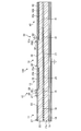
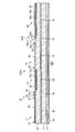
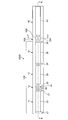
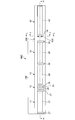
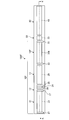
- FIG. 1 is a schematic top view of the wavelength tunable laser element according to the first embodiment.
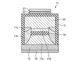
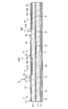
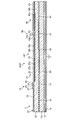
- FIG. 2 is a sectional view of the wavelength tunable laser element shown in FIG. 1 taken along the line AA.
- FIG. 3 is a sectional view of the wavelength tunable laser element shown in FIG. 1 taken along line BB.
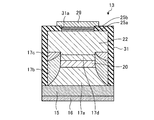
- FIG. 4 is a sectional view taken along line CC of the wavelength tunable laser element shown in FIG.
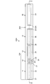
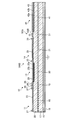
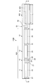
- FIG. 5 is a schematic top view of the wavelength tunable laser element according to the second embodiment.
- FIG. 6 is a sectional view taken along the line DD of the wavelength tunable laser element shown in FIG.
- FIG. 7 is a schematic top view of the wavelength tunable laser element according to the third embodiment.
- FIG. 1 is a schematic top view of the wavelength tunable laser element according to the first embodiment.
- FIG. 2 is a sectional view of the wavelength tunable laser element shown in FIG. 1 taken along the line AA.
- FIG. 3 is
- FIG. 8 is a sectional view taken along the line EE of the wavelength tunable laser element shown in FIG.
- FIG. 9 is a sectional view taken along line FF of the wavelength tunable laser element shown in FIG.
- FIG. 10 is a schematic top view of the wavelength tunable laser element according to the fourth embodiment.
- FIG. 11 is a sectional view taken along the line GG of the wavelength tunable laser element shown in FIG.
- FIG. 12 is a schematic top view of the wavelength tunable laser element according to the fifth embodiment.
- FIG. 13 is a sectional view taken along the line HH of the wavelength tunable laser element shown in FIG.
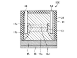
- FIG. 14A is a sectional view taken along the line JJ of the wavelength tunable laser element shown in FIG. FIG.
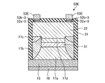
- FIG. 14B is a sectional view taken along line LL of the wavelength tunable laser element shown in FIG.
- FIG. 15 is a schematic top view of the wavelength tunable laser device according to the sixth embodiment.
- FIG. 16 is a sectional view taken along line KK of the wavelength tunable laser element shown in FIG.
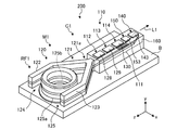
- FIG. 17 is a schematic perspective view of the wavelength tunable laser device according to the seventh embodiment.
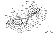
- FIG. 18 is a schematic perspective view of the wavelength tunable laser element according to the eighth embodiment.
- FIG. 1 is a schematic top view of the wavelength tunable laser element 100 according to the first embodiment
- FIG. 2 is a sectional view taken along the line AA of the wavelength tunable laser element 100 shown in FIG. 1
- FIG. 3 is shown in FIG. 4 is a sectional view of the wavelength tunable laser element 100 taken along line BB
- FIG. 4 is a sectional view of the wavelength tunable laser element 100 taken along line CC of FIG.
- illustration of a part of the configuration (protective film, spacer layer) is omitted.
- the wavelength tunable laser device 100 is a semiconductor optical integrated device in which a semiconductor laser 10, a semiconductor optical amplifier (SOA) 40 which is a forward bias optical device, and a passive waveguide portion 50 are monolithically integrated on the upper surface of a semiconductor substrate 15. .
- the forward-biased optical element means a device in which a current is passed from the electrode placed above the forward-bias electrode to the electrode placed below.
- the semiconductor laser 10 has a first SG-DBR (Sampled Grating Distributed Bragg Reflector) 11, which is a mirror having a length, a phase adjusting unit 12, a gain unit 13, and a second SG-DBR 14.
- the first SG-DBR 11, the phase adjustment unit 12, the gain unit 13, and the second SG-DBR 14 are connected in this order.
- the first SG-DBR 11 is one in which the second reflecting section and the wavelength filter are integrally configured.
- the first SG-DBR 11 includes, for example, a lower cladding layer 17a made of n-type InP and an optical waveguide layer 18 having a DBR-type diffraction grating layer on the main surface of a semiconductor substrate 15 made of n-type InP.
- a spacer layer 17d made of p-type InP and an upper cladding layer 22 made of p-type InGaAsP are sequentially stacked, and a micro-heater 23 which is a resistance heater containing Ti and AuZn are provided above the protective film 31 made of SiN or the like.
- the pad electrode 27 including is disposed.
- the wavelength characteristic of the first SG-DBR 11 can be adjusted by changing the refractive index of the optical waveguide layer 18 due to the heating of the micro heater 23.
- the optical waveguide layer 18 and the spacer layer 17d have a stripe mesa structure having a width (for example, 1.8 ⁇ m) suitable for optically guiding the 1.55 ⁇ m band light in a single mode by etching or the like.
- the striped mesa structure has a buried structure having a current blocking structure composed of a p-type InP buried layer 17b and an n-type InP current blocking layer 17c on both sides (left and right in the drawing).
- the optical waveguide layer 18 has a structure in which a sampling diffraction grating is formed in the p-type InGaAsP layer along the z direction, and the groove of the diffraction grating is filled with InP.
- the grating spacing of the diffraction grating is constant but is sampled, so that a reflection response substantially periodic with respect to the wavelength is exhibited.
- the phase adjustment unit 12 is provided between the first SG-DBR 11 and the second SG-DBR 14.
- a lower clad layer 17a, an optical waveguide layer 19 made of InGaAsP, a spacer layer 17d, and an upper clad layer 22 are sequentially laminated on the main surface of the semiconductor substrate 15, and the lower clad layer 17a, the spacer layer 17d, and the upper clad layer 22 are sequentially stacked on the main surface.
- a micro-heater 24 which is a resistance heater containing Ti and a pad electrode 28 containing AuZn are arranged.
- the cross section of the phase adjusting portion has a structure in which the optical waveguide layer 18 having the DBR type diffraction grating layer of the first SG-DBR 11 shown in FIG.
- the gain unit 13 is provided between the first SG-DBR 11 and the second SG-DBR 14 and exerts an optical amplification function by being supplied with a drive current.
- the gain section 13 includes a lower clad layer 17a, an active core layer 20 made of InGaAsP, a spacer layer 17d, and an upper clad layer 22, which are sequentially stacked on the main surface of the semiconductor substrate 15, and the upper clad layer is formed.
- a pad electrode 29 containing AuZn is arranged on the upper part of the electrode 22 via a contact layer 25a and an ohmic electrode 25b.
- the contact layer 25a and the ohmic electrode 25b are provided in the opening 31a formed in the protective film 31.
- the active core layer 20 and the spacer layer 17d have a stripe mesa structure having a width (for example, 1.8 ⁇ m) suitable for optical waveguide of 1.55 ⁇ m band light in a single mode by etching or the like. Both sides (in the left-right direction of the paper) have a buried structure having a current blocking structure composed of a p-type InP buried layer 17b and an n-type InP current blocking layer 17c.
- the second SG-DBR 14 is configured by integrally forming a first reflecting portion that outputs laser light and a wavelength filter.
- the second SG-DBR 14 has a lower clad layer 17a, an optical waveguide layer 21 having a DBR type diffraction grating layer, a spacer layer 17d, and an upper clad layer 22, which are sequentially stacked on the main surface of the semiconductor substrate 15, and is made of SiN or the like for protection.
- a micro-heater 26, which is a resistance heater containing Ti, and a pad electrode 30 containing AuZn are arranged on the upper part of the film 31.
- the optical waveguide layer 21 has a configuration in which a sampling diffraction grating is formed in the p-type InGaAsP layer along the z direction, and the groove of the diffraction grating is filled with InP.
- the cross section of the second SG-DBR 14 is similar to that of the first SG-DBR 11 of FIG.
- the diffraction grating has a constant grating interval, but is sampled, and this shows a reflection response that is substantially periodic with respect to the wavelength.
- the wavelength characteristic of the second SG-DBR 14 can be adjusted by changing the refractive index of the optical waveguide layer 21 due to the heating of the micro heater 26.
- the first SG-DBR 11 and the second SG-DBR 14 form a laser resonator.
- the first SG-DBR 11 and the second SG-DBR 14 have periodic reflection peaks having different wavelength intervals as wavelength characteristics.
- the SOA 40 is provided on the semiconductor substrate 15 on the laser light output side of the second SG-DBR 14 via a passive waveguide section 50 described later.
- a lower clad layer 17a, an active core layer 41, a spacer layer 17d, and an upper clad layer 22 are sequentially stacked on the main surface of the semiconductor substrate 15, and a contact layer 42a and an ohmic electrode 42b are formed on the upper clad layer 22.
- the pad electrode 43 containing AuZn is disposed therethrough.
- the contact layer 42a and the ohmic electrode 42b are provided in the opening 31a formed in the protective film 31 made of SiN or the like.
- the cross section of the SOA 40 is similar to that of the gain section 13 shown in FIG. When the SOA 40 is supplied with the drive current, the SOA 40 amplifies the laser light output from the second SG-DBR 14 and outputs it as high-power laser light from the end face of the tunable laser element 100.
- the wavelength of laser light is, for example, in the range of 1.55 ⁇ m wavelength band.
- the end face be coated with an antireflection coating.
- the antireflection coating may be applied only to the end surface on the SOA 40 side, the number of coating steps can be reduced.
- the active core layer 41 of the SOA 40 be tilted in the vicinity of the end face with respect to the normal line of the end face by several degrees, typically 7°.
- the passive waveguide section 50 is provided between the second SG-DBR 14 and the SOA 40, and connects the semiconductor laser 10 and the SOA 40 with the optical waveguide layer 51.
- a lower clad layer 17a made of n-type InP, an optical waveguide layer 51 made of InGaAsP, a spacer layer 17d, and an upper clad layer 22 are sequentially laminated on the main surface of the semiconductor substrate 15, and the upper clad layer is formed.
- a passive waveguide electrode 53 containing AuZn is arranged on the upper part of 22 via a contact layer 52a and an ohmic electrode 52b.
- the contact layer 52a and the ohmic electrode 52b are provided in the opening 31a formed in the protective film 31 made of SiN or the like.
- the cross section of the passive waveguide portion 50 has a structure in which the active core layer 20 of the gain portion 13 shown in FIG. 4 is replaced with an optical waveguide layer 51.
- the ground electrode 16 is configured to include AuGeNi, for example, and is in ohmic contact with the semiconductor substrate 15.
- the pad electrode 29 of the gain section 13, the pad electrode 43 of the SOA 40, and the passive waveguide electrode 53 are p-side electrodes, and the passive waveguide electrode 53 is electrically connected to the ground electrode 16.
- the wavelength of the laser light can be adjusted by adjusting the wavelength characteristics of the first SG-DBR 11 and the second SG-DBR 14 by the micro heaters 24 and 26, and functions as a vernier type wavelength tunable laser. To do.
- the leakage current from the SOA 40 through the upper clad layer 22 flows to the optical waveguide layer 21 of the second SG-DBR 14. Since the refractive index of the optical waveguide layer 21 changes, the reflection phase of the second SG-DBR 14 may change and the spectral line width may become broad. Further, in the wavelength tunable laser device 100 including the SOA 40, since the optical output is adjusted using the SOA, the leakage current amount may be increased or decreased by the optical output, and the spectral line width may be changed by the optical output. Furthermore, when the current injected into the active core layer 41 of the SOA 40 fluctuates due to an external factor, the amount of leakage current also changes and the spectral line width becomes broad.
- the passive waveguide section 50 is arranged between the second SG-DBR 14 and the SOA 40, and the leakage current from the SOA 40 can be passed to the ground electrode 16 via the passive waveguide electrode 53, so that the leakage occurs. It is possible to suppress the broadening of the spectral line width due to the electric current.
- the SOA is described as an example of the forward bias optical element, but the present invention is not limited to this.
- a current injection type filter can be used instead of the SOA.
- FIG. 5 is a schematic top view of the wavelength tunable laser element 100A according to the second embodiment
- FIG. 6 is a sectional view taken along line DD of the wavelength tunable laser element 100A shown in FIG.
- illustration of a part of the structure (protective film, spacer layer) is omitted.
- the passive waveguide electrode 53A of the passive waveguide portion 50A is formed shorter than the length of the passive waveguide portion 50A.
- the contact layer 52a-1 and the ohmic electrode 52b-1 are also formed short like the passive waveguide electrode 53A.
- the passive waveguide section 50 is arranged between the second SG-DBR 14 and the SOA 40, and the leakage current from the SOA 40 is extracted to suppress the broadening of the spectral line width. Since the contact layer 52a made of P-type InGaAsP having a high doping concentration is provided on the upper portion, light loss occurs due to light absorption of the contact layer 52a. In the second embodiment, the length of the passive waveguide electrode 53A is made shorter than the length of the passive waveguide portion 50A, thereby reducing the light loss due to the contact layer 52a-1.
- the passive waveguide electrode 53 is provided over the entire length of the passive waveguide portion 50 except for the electrically insulating gap (usually about 10 ⁇ m each) from the second SG-DBR 14 and the SOA 40.
- the second passive waveguide electrode 53A has a length of 80% or less of the length of the passive waveguide portion 50A, preferably 10% or more and 50% or less of the length of the passive waveguide portion 50A.
- the length of the passive waveguide portion 50A does not include an electrically insulating gap.
- the passive waveguide electrode 53A is preferably installed on the SOA 40 side.
- the passive waveguide electrode 53A similarly to the first embodiment, by extracting the leakage current from the SOA 40 by the passive waveguide electrode 53A, it is possible to suppress the broadening of the spectral line width due to the leakage current and to increase the length of the passive waveguide electrode 53A. Is short, it is possible to reduce light loss.
- FIG. 7 is a schematic top view of the wavelength tunable laser element 100B according to the third embodiment
- FIG. 8 is a sectional view taken along line EE of the wavelength tunable laser element 100B shown in FIG. 7, and
- FIG. 8 is a cross-sectional view taken along the line FF of the wavelength tunable laser element 100B shown in FIG.
- illustration of part of the structure (protective film, spacer layer) is omitted.
- the passive waveguide electrode 53B of the passive waveguide portion 50B is arranged so as not to be directly above the optical waveguide layer 51.
- the contact layer 52a-2 and the ohmic electrode 52b-2 are also arranged so as not to be directly above the optical waveguide layer 51.
- providing the contact layer 52a on the optical waveguide layer 51 causes light loss due to light absorption of the contact layer 52a.
- two contact layers 52a-2, an ohmic electrode 52b-2, and a passive waveguide electrode 53B are formed in parallel with the optical waveguide layer 51 of the passive waveguide portion 50B, and the layer immediately above the optical waveguide layer 51 is formed. Avoid it.
- the passive waveguide electrode 53A similarly to the first embodiment, by extracting the leakage current from the SOA 40 by the passive waveguide electrode 53A, it is possible to suppress the broadening of the spectral line width due to the leakage current, and the passive waveguide electrode 53B is used as the optical waveguide. Since it is arranged so as not to be directly above the layer 51, it is possible to reduce light loss.
- FIG. 10 is a schematic top view of the wavelength tunable laser element 100D according to the fourth embodiment
- FIG. 11 is a sectional view taken along the line GG of the wavelength tunable laser element 100D shown in FIG.
- illustration of a part of the structure (protective film, spacer layer) is omitted.
- the pad electrode 43D of the SOA 40D is formed to have a length shorter than that of the active core layer 41.
- the contact layer 42a-1 and the ohmic electrode 42b-1 are also formed short like the pad electrode 43D.
- the leakage current from the pad electrode 43 of the SOA 40 is extracted by the passive waveguide electrode 53 of the passive waveguide section 50, thereby suppressing the broadening of the spectrum line width.
- the amount of leakage current from the pad electrode 43 of the SOA 40 is reduced to further suppress the broadening of the spectral line width.
- the length r1 of the pad electrode 43 of the SOA 40D is shorter than the length r2 of the active core layer 41, and the pad electrode 43D is located on the end of the active core layer 41 on the passive waveguide section 50 side. Not placed.
- the length of the portion of the active core layer 41 where the pad electrode 43D is not disposed (excluding the electrical insulation gap). ) Is preferably 10 ⁇ m or less.
- the leakage current from the SOA 40 is extracted by the passive waveguide electrode 53A, so that broadening of the spectral line width due to the leakage current can be suppressed, and leakage from the pad electrode 43D of the SOA 40D can be suppressed. Since the amount of current is reduced, it is possible to further broaden the spectral line width.
- the same passive waveguide section 50 as in the first embodiment is adopted, but the passive waveguide section 50A of the second embodiment and the passive waveguide section 50B of the third embodiment are also adopted. Good.
- FIG. 5 is a schematic top view of the wavelength tunable laser element 100E according to the fifth embodiment
- FIG. 13 is a sectional view taken along the line HH of the wavelength tunable laser element 100E shown in FIG. 12
- FIG. 14A is FIG. 13 is a cross-sectional view (cross section at groove 54) of the wavelength tunable laser element 100E shown in FIG.
- FIG. 14B is a cross-sectional view (cross section at the passive waveguide electrode 53E) of the wavelength tunable laser element shown in FIG. 12, taken along the line LL.
- illustration of a part of the structure (protective film, spacer layer) is omitted.
- the wavelength tunable laser device 100E according to the fifth embodiment has the groove 54 on the SOA 40 side with respect to the passive waveguide electrode 53E.
- the groove portion 54 is formed on the SOA 40 side of the passive waveguide electrode 53E.
- Two grooves 54, the contact layer 52a-3, the ohmic electrode 52b-3, and the passive waveguide electrode 53E are formed in parallel with the optical waveguide layer 51 of the passive waveguide portion 50E, and are formed directly above the optical waveguide layer 51. Avoid it.
- the contact layer 52a-3, the ohmic electrode 52b-3, and the passive waveguide electrode 53E are shorter than the passive waveguide portion 50E, and are arranged adjacent to the groove portion 54.
- the groove 54 reduces the injection of the leakage current from the SOA 40 into the passive waveguide electrode 53E. Since the leak current flows through the upper clad layer 22, it is preferable that the groove 54 be provided up to the n-type InP current blocking layer 17c through the p-type InP buried layer 17b.
- the width of the passive waveguide electrode 53E (length in the direction orthogonal to the optical waveguide layer 51) is made longer than the width of the groove 54, thereby improving the amount of leakage current drawn by the passive waveguide electrode 53E.
- the length may be the same as that of the groove 54.
- the fifth embodiment similarly to the first embodiment, by extracting the leakage current from the SOA 40 by the passive waveguide electrode 53E, it is possible to suppress the broadening of the spectral line width due to the leakage current, and the groove 54 allows the pad electrode 43 of the SOA 40 to be suppressed. Since the amount of leakage current that can be injected from the device can be reduced, it is possible to further broaden the spectral line width.
- FIG. 15 is a schematic top view of the wavelength tunable laser element 100F according to the fifth embodiment
- FIG. 16 is a sectional view taken along the line KK of the wavelength tunable laser element 100F shown in FIG.
- illustration of a part of the structure (protective film, spacer layer) is omitted.
- the second SG-DBR 14F is a current injection type.
- the second SG-DBR 14F is a pad electrode containing AuZn via the contact layer 32a and the ohmic electrode 32b on the upper clad layer 22 instead of the micro heater 26 and the pad electrode 30 in the second SG-DBR 14 of the first embodiment. 33 are arranged.
- the contact layer 32a and the ohmic electrode 32b are provided in the opening formed in the protective film 31 made of SiN or the like.
- current is injected from the ground electrode 16 and the pad electrode 33 into the optical waveguide layer 21 having the diffraction grating layer.
- the concentration of electrons and holes in the optical waveguide layer 21 forming the distributed reflector changes.
- the refractive index changes due to the carrier plasma effect, and the wavelength characteristics can be changed.
- the second SG-DBR 14F is a current injection type, it is possible to suppress the broadening of the spectrum line width due to the leakage current by extracting the leakage current from the SOA 40 by the passive waveguide electrode 53.
- FIG. 17 is a schematic perspective view of the wavelength tunable laser device 200 according to the seventh embodiment.
- the mirrors having two lengths are the SG-DBR 114 and the ring resonator filter RF1.
- the wavelength tunable laser element 200 is configured to oscillate in the 1.55 ⁇ m band and output a laser beam L1.
- the wavelength tunable laser element 200 includes a first waveguide section 110 and a second waveguide section 120 formed on a common semiconductor substrate B.
- the semiconductor substrate B is, for example, an n-type InP substrate.
- a ground electrode is formed on the back surface of the semiconductor substrate B.
- the ground electrode is made of, for example, AuGeNi and is in ohmic contact with the semiconductor substrate B.
- the first waveguide section 110 includes a phase adjustment section 112, a gain section 113, an SG-DBR 114, a passive waveguide section 150, and an SOA 140. Further, the first waveguide section 110 includes a micro-heater 128, a pad electrode 129, a micro-heater 130, a passive waveguide on the phase adjusting section 112, the gain section 113, the SG-DBR 114, the passive waveguide section 150, and the SOA 140. It has an electrode 153 and a pad electrode 143.
- the waveguide section 111 to which the layer and the active core layer of the SOA 140 are connected is arranged.
- the semiconductor laminated portion 160 is configured by laminating semiconductor layers, and has the function of a clad portion with respect to the waveguide portion 111.
- the microheater 128, the pad electrode 129, the microheater 130, the passive waveguide electrode 153, and the pad electrode 143 are arranged on the semiconductor laminated portion 160 along the waveguide portion 111.
- a SiN x protective film is formed on the semiconductor laminated portion 160, and the pad electrode 129, the passive waveguide electrode 153, and the pad electrode 143 are provided on the semiconductor laminated portion 160 via the openings formed in the SiN x protective film. Is in contact with.
- the second waveguide section 120 includes a bifurcating section 121, two arm sections 122 and 123, a ring-shaped waveguide 124, and a micro heater 125 made of Ti.
- the 2-branching part 121 is configured by a 1 ⁇ 2 type branching waveguide including a 1 ⁇ 2 type multimode interference (MMI) waveguide 121a, and the 2-port side is connected to each of the two arm parts 122 and 123. At the same time, the 1-port side is connected to the first waveguide section 110 side.
- MMI multimode interference
- the arm portions 122 and 123 both extend in the z direction and are arranged so as to sandwich the ring-shaped waveguide 124.
- the arm portions 122 and 123 are close to the ring-shaped waveguide 124, and both are optically coupled to the ring-shaped waveguide 124 with the same coupling coefficient ⁇ .
- the value of ⁇ is 0.2, for example.
- the arm portions 122 and 123 and the ring-shaped waveguide 124 form a ring resonance filter RF1.
- the ring resonance type filter RF1 and the bifurcating part 121 form a reflection mirror M1.
- the reflection mirror M1 exhibits a reflection response that is substantially periodic with respect to the wavelength.
- the microheaters 125a and 125b as heating units for heating the optical waveguide are ring-shaped.
- the micro heater 125a is arranged on the outer peripheral side of the ring-shaped waveguide 124, and the micro heater 125b is arranged on the inner peripheral side.
- the microheaters 125a and 125b are provided on a dielectric layer as a protective film formed so as to cover the ring-shaped waveguide 124.
- the first waveguide section 110 and the second waveguide section 120 are optically connected to each other, and the waveguide layer having the diffraction grating layer of the waveguide section 111 and the reflection mirror M1 constitute a laser resonator C1. doing. Further, the phase adjusting unit 112, the gain unit 113, the SG-DBR 114, and the second waveguide unit 120 form a semiconductor laser.
- the ring-shaped waveguide 124 has a high-mesa waveguide structure. The width of the high mesa waveguide structure is about 2 ⁇ m.
- the wavelength of the laser light can be adjusted by adjusting the wavelength characteristics of the SG-DBR 114 and the reflection mirror M1 by the microheaters 130 and 125, and the wavelength tunable laser element functions as a vernier type wavelength tunable laser.
- the passive waveguide electrode 153 of the passive waveguide unit 150 can extract the leakage current from the SOA 140, so that broadening of the spectral line width can be prevented.
- the passive waveguide section 150 between the SOA 140 and the SG-DBR 114, leakage occurs. It is possible to suppress the broadening of the spectral line width due to the electric current.
- FIG. 18 is a schematic perspective view of the wavelength tunable laser element 200G according to the eighth embodiment.
- the mirrors having two lengths are the SG-DBR 114 and the ring resonator filter RF2
- the phase adjusting unit 112 includes the two arm units 122 and 123G of the second waveguide unit 120. It is provided on one of the arm portions 123G.
- the wavelength tunable laser device 200G is configured to oscillate in the 1.55 ⁇ m band and output a laser beam L1.
- the wavelength tunable laser device 200G includes a first waveguide section 110G and a second waveguide section 120G formed on a common semiconductor substrate S1.
- the semiconductor substrate S1 is, for example, an n-type InP substrate.
- a ground electrode is formed on the back surface of the semiconductor substrate S1.
- the ground electrode is made of, for example, AuGeNi, and makes ohmic contact with the semiconductor substrate S1.
- the first waveguide section 110G includes a gain section 113, an SG-DBR 114, a passive waveguide section 150, and an SOA 140. Further, the first waveguide section 110G has a pad electrode 129, a micro heater 130, a passive waveguide electrode 153, and a pad electrode 143 on the gain section 113, SG-DBR 114, passive waveguide section 150, and SOA 140. doing. Inside the first waveguide section 110G, the active core layer of the gain section 113, the waveguide layer having the diffraction grating layer of the SG-DBR 114, the waveguide layer of the passive waveguide section 150, and the active core layer of the SOA 140 are provided. The connected waveguide section 111G is arranged.
- the semiconductor laminated portion 160 is formed by laminating semiconductor layers, and has a function of a cladding portion and the like with respect to the waveguide portion 111G.
- the pad electrode 129, the micro heater 130, the passive waveguide electrode 153, and the pad electrode 143 are arranged on the semiconductor laminated portion 160 along the waveguide portion 111G.
- a SiN x protective film is formed on the semiconductor laminated portion 160, and the pad electrode 129, the passive waveguide electrode 153, and the pad electrode 143 are provided on the semiconductor laminated portion 160 via the openings formed in the SiN x protective film. Is in contact with.
- the second waveguide section 120G includes a bifurcating section 121, two arm sections 122 and 123G, a ring-shaped waveguide 124, and a micro heater 125 made of Ti.
- the 2-branching part 121 is configured by a 1 ⁇ 2 type branching waveguide including a 1 ⁇ 2 type multimode interference (MMI) waveguide 121a, and the 2-port side is connected to each of the two arm parts 122 and 123G. In addition, the 1-port side is connected to the first waveguide section 110G side.
- MMI multimode interference
- the arm portions 122 and 123G and the ring-shaped waveguide 124 form a ring resonance type filter RF2.
- the ring resonance type filter RF2 and the two-branching part 121 form a reflection mirror M2.
- Each of the arm portions 122 and 123G extends in the z direction and is arranged so as to sandwich the ring-shaped waveguide 124.
- the phase adjuster 112 is arranged on the arm 123G.
- a micro heater 128 is formed on the phase adjustment unit 112.
- the arm portion 123G is configured by laminating a lower clad layer made of n-type InP, an optical waveguide layer made of InGaAsP, and an upper clad layer made of p-type InP on the semiconductor substrate S1 in this order. Has a high mesa waveguide structure.
- the SiN protective film is formed so as to cover the arm portion 123G.
- the micro-heater 128 is arranged on the SiN protective film along the optical waveguide layer of the phase adjusting unit 112.
- the second branch portion 121, the arm portion 122, and the ring-shaped waveguide 124, which are other components of the second waveguide portion 120G, also have a high-mesa waveguide structure and are covered with the SiN protective film.
- the micro-heater 125 has a ring shape and is disposed on the SiN protective film formed so as to cover the ring-shaped waveguide 124.
- the first waveguide section 110G and the second waveguide section 120G are optically connected to each other, and the waveguide layer having the diffraction grating layer of the waveguide section 111G and the reflection mirror M2 constitute a laser resonator C2. doing. Further, the gain section 113, the SG-DBR 114, and the second waveguide section 120G form a semiconductor laser.
- the passive waveguide electrode 153 of the passive waveguide unit 150 can extract the leakage current from the SOA 140, and thus the broadening of the spectral line width can be prevented.
- the passive waveguide section 150 is arranged between the SOA 140 and the SG-DBR 114 to prevent leakage. It is possible to suppress the broadening of the spectral line width due to the electric current.
- the present invention is not limited to the above embodiment.
- the present invention also includes those configured by appropriately combining the above-described components. Further, further effects and modified examples can be easily derived by those skilled in the art. Therefore, the broader aspects of the present invention are not limited to the above embodiments, and various modifications can be made.
- the semiconductor optical integrated device according to the present invention is useful for an optical device used for optical communication and the like.
Landscapes
- Physics & Mathematics (AREA)
- General Physics & Mathematics (AREA)
- Optics & Photonics (AREA)
- Condensed Matter Physics & Semiconductors (AREA)
- Electromagnetism (AREA)
- Geometry (AREA)
- Engineering & Computer Science (AREA)
- Microelectronics & Electronic Packaging (AREA)
- Semiconductor Lasers (AREA)
- Optical Integrated Circuits (AREA)
Abstract
半導体光増幅器等の順バイアス光素子からの漏れ電流のミラーへの流入を抑制し、スペクトル線幅のブロード化を防止しうる半導体光集積素子を提供することを目的とする。半導体光集積素子は、半導体基板の上面に、順バイアス光素子と半導体レーザがモノリシック集積された半導体光集積素子であって、前記順バイアス光素子と前記半導体レーザの間に配置される受動導波路部と、前記半導体基板の下面に配置される接地電極と、を備え、前記半導体レーザは、長さを有するミラーを前記順バイアス光素子側に有し、前記順バイアス光素子は、前記半導体基板と接する側と反対側に順バイアス光素子電極を有し、前記受動導波路部は、前記半導体基板と接する側と反対側に受動導波路電極を有し、前記受動導波路電極は、前記接地電極と電気的に接続されている。
Description
本発明は、順バイアス光素子と半導体レーザがモノリシック集積された半導体光集積素子に関する。
コヒーレント光通信の普及に伴って、発振したレーザ光が狭スペクトル線幅である波長可変レーザ素子の需要が高まっている。波長可変レーザ素子の1つに標本化回折格子(Sampled Grating)を用い、かつバーニア効果を利用した分布ブラッグ反射(DBR:Distributed Bragg Reflector)型波長可変レーザがある(たとえば特許文献1および2参照)。この波長可変レーザ素子においては、半導体素子内に回折格子の一部が標本化されたDBRミラーを2つ用いる。この2つのDBRミラーの反射スペクトルは、周期がわずかに異なる櫛状のピークを有する形状をしている。また、DBRミラーに電流注入または加熱により屈折率変化を起して、その反射波長特性を可変にできる。2つのDBRミラーの反射ピークを重ね合わせることにより、この重ね合わせた波長で共振器を形成することができる。このとき、共振器長を適切に設計すれば、共振器モードである縦モードの間隔が2つのDBRミラーによる反射ピークの帯域と同程度となり、1つの共振器モードだけが選択され、単一モード発振が実現される。
特許文献1,2においては、レーザーキャビティの外に半導体光増幅器(SOA:Semiconductor Optical Amplifier)を備えているが、半導体光増幅器からのリーク電流が隣接するDBRミラーの導波路部に流入して、DBRミラーの屈折率が変動するためにスペクトル線幅がブロード化してしまうという問題を有していた。
本発明は、上記に鑑みてなされたものであって、半導体光増幅器等の順バイアス光素子からの漏れ電流のミラーへの流入を抑制し、スペクトル線幅のブロード化を防止しうる半導体光集積素子を提供することを目的とする。
上述した課題を解決し、目的を達成するために、本発明の一態様に係る半導体光集積素子は、半導体基板の上面に、順バイアス光素子と半導体レーザがモノリシック集積された半導体光集積素子であって、前記順バイアス光素子と前記半導体レーザの間に配置される受動導波路部と、前記半導体基板の下面に配置される接地電極と、を備え、前記半導体レーザは、長さを有するミラーを前記順バイアス光素子側に有し、前記順バイアス光素子は、前記半導体基板と接する側と反対側に順バイアス光素子電極を有し、前記受動導波路部は、前記半導体基板と接する側と反対側に受動導波路電極を有し、前記受動導波路電極は、前記接地電極と電気的に接続されている。
また、本発明の一態様に係る半導体光集積素子は、前記順バイアス光素子は、半導体光増幅器である。
また、本発明の一態様に係る半導体光集積素子は、前記受動導波路電極の長さは、前記受動導波路部の長さより短い。
また、本発明の一態様に係る半導体光集積素子は、前記受動導波路電極は、前記受動導波路部に光導波路層の直上を避けて配置されている。
また、本発明の一態様に係る半導体光集積素子は、前記順バイアス光素子電極の長さは、前記順バイアス光素子の活性コア層の長さより短く、前記順バイアス光素子電極は、前記活性コア層の前記受動導波路部側の端部上に配置されていない。
また、本発明の一態様に係る半導体光集積素子は、受動導波路部は、前記受動導波路電極より順バイアス光素子側に溝部を有する。
また、本発明の一態様に係る半導体光集積素子は、前記半導体レーザは波長可変レーザであり、2つの前記長さを有するミラーと、利得導波路部と、位相調整導波路部と、を有する。
また、本発明の一態様に係る半導体光集積素子は、前記2つの長さを有するミラーのうち、少なくとも1つは分布ブラッグ反射器である。
また、本発明の一態様に係る半導体光集積素子は、前記2つの長さを有するミラーは、前記分布ブラッグ反射器とリング共振器フィルタである。
また、本発明の一態様に係る半導体光集積素子は、前記2つの長さを有するミラーのうち、順バイアス光素子側に配置される長さを有するミラーはヒータにより制御される。
本発明によれば、半導体光増幅器等からの漏れ電流のミラーへの流入を抑制し、狭スペクトル線幅の半導体光集積素子を実現できるという効果を奏する。
以下に、図面を参照して実施形態を詳細に説明する。なお、この実施形態によりこの発明が限定されるものではない。また、各図面において、同一または対応する要素には適宜同一の符号を付している。さらに、図面は模式的なものであり、各要素の寸法の関係、各要素の比率などは、現実のものとは異なる場合があることに留意する必要がある。図面の相互間においても、互いの寸法の関係や比率が異なる部分が含まれている場合がある。また、一部の図中においては、適宜xyz座標軸を示し、これにより方向を説明する。
(実施形態1)
図1は、実施形態1に係る波長可変レーザ素子100の模式的な上面図、図2は、図1に示す波長可変レーザ素子100のA-A線断面図、図3は、図1に示す波長可変レーザ素子100のB-B線断面図、図4は、図1に示す波長可変レーザ素子100のC-C線断面図である。なお、図2では、一部構成(保護膜、スペーサ層)の図示を省略している。
図1は、実施形態1に係る波長可変レーザ素子100の模式的な上面図、図2は、図1に示す波長可変レーザ素子100のA-A線断面図、図3は、図1に示す波長可変レーザ素子100のB-B線断面図、図4は、図1に示す波長可変レーザ素子100のC-C線断面図である。なお、図2では、一部構成(保護膜、スペーサ層)の図示を省略している。
波長可変レーザ素子100は、半導体基板15の上面に、半導体レーザ10と、順バイアス光素子である半導体光増幅器(SOA)40と、受動導波路部50がモノシリック集積された半導体光集積素子である。なお、本明細書において、順バイアス光素子とは、順バイアス電極の上部に設置された電極から下部に設置された電極に電流を流すデバイスを意味する。
半導体レーザ10は、長さを有するミラーである第1SG-DBR(Sampled Grating Distributed Bragg Reflector)11と、位相調整部12と、利得部13と、第2SG-DBR14とを有する。第1SG-DBR11、位相調整部12、利得部13、および第2SG-DBR14は、この順番に接続されている。
第1SG-DBR11は、第2反射部と波長フィルタとが一体に構成されたものである。第1SG-DBR11は、図3に示すように、たとえば、n型InPからなる半導体基板15の主面上に、n型InPからなる下部クラッド層17a、DBR型回折格子層を有する光導波路層18、p型InPからなるスペーサ層17d、p型InGaAsPからなる上部クラッド層22が順次積層され、SiN等からなる保護膜31を介して、上部にTiを含む抵抗ヒータであるマイクロヒータ23と、AuZnを含むパッド電極27が配置されている。第1SG-DBR11は、マイクロヒータ23の加熱による光導波路層18の屈折率の変化によって、波長特性を調整可能である。
光導波路層18およびスペーサ層17dは、エッチング等により、1.55μm帯の光をシングルモードで光導波するのに適した幅(例えば1.8μm)にされたストライプメサ構造とされている。ストライプメサ構造の両脇(紙面左右方向)は、p型InP埋め込み層17bおよびn型InP電流ブロッキング層17cからなる電流ブロッキング構造を有した埋込み構造となっている。光導波路層18は、p型InGaAsP層にz方向に沿って標本化回折格子が形成され、回折格子の溝はInPで埋め込まれた構成を有する。光導波路層18において回折格子の格子間隔は一定であるが標本化されており、これにより波長に対し略周期的な反射応答を示す。
位相調整部12は、第1SG-DBR11と第2SG-DBR14との間に設けられている。位相調整部12は、半導体基板15の主面上に、下部クラッド層17a、InGaAsPからなる光導波路層19、スペーサ層17d、上部クラッド層22が順次積層され、保護膜31を介して、上部にTiを含む抵抗ヒータであるマイクロヒータ24と、AuZnを含むパッド電極28が配置されている。位相調整部の断面は、図3に示す第1SG-DBR11のDBR型回折格子層を有する光導波路層18が、光導波路層19に置き換えられた構造である。
利得部13は、第1SG-DBR11と第2SG-DBR14との間に設けられており、駆動電流を供給されることによって光増幅機能を発揮する。利得部13は、図4に示すように、半導体基板15の主面上に、下部クラッド層17a、InGaAsPからなる活性コア層20、スペーサ層17d、上部クラッド層22が順次積層され、上部クラッド層22の上部にコンタクト層25aおよびオーミック電極25bを介して、AuZnを含むパッド電極29が配置されている。コンタクト層25aおよびオーミック電極25bは、保護膜31に形成された開口部31aに設けられている。活性コア層20およびスペーサ層17dは、エッチング等により、1.55μm帯の光をシングルモードで光導波するのに適した幅(例えば1.8μm)にされたストライプメサ構造とされ、ストライプメサ構造の両脇(紙面左右方向)は、p型InP埋め込み層17bおよびn型InP電流ブロッキング層17cからなる電流ブロッキング構造を有した埋込み構造となっている。
第2SG-DBR14は、レーザ光が出力される第1反射部と波長フィルタとが一体に構成されたものである。第2SG-DBR14は、半導体基板15の主面上に、下部クラッド層17a、DBR型回折格子層を有する光導波路層21、スペーサ層17d、上部クラッド層22が順次積層され、SiN等からなる保護膜31を介して、上部にTiを含む抵抗ヒータであるマイクロヒータ26と、AuZnを含むパッド電極30が配置されている。光導波路層21は、光導波路層18と同様に、p型InGaAsP層にz方向に沿って標本化回折格子が形成され、回折格子の溝はInPで埋め込まれた構成を有する。第2SG-DBR14の断面は、図3の第1SG-DBR11と同様である。光導波路層21において回折格子の格子間隔は一定であるが標本化されており、これにより波長に対し略周期的な反射応答を示す。第2SG-DBR14は、マイクロヒータ26の加熱による光導波路層21の屈折率の変化によって、波長特性を調整可能である。第1SG-DBR11と第2SG-DBR14とがレーザ共振器を構成している。第1SG-DBR11と第2SG-DBR14とは、波長特性として、互いに波長間隔が異なる周期的な反射ピークを有している。
SOA40は、半導体基板15上において、後述する受動導波路部50を介して、第2SG-DBR14のレーザ光出力側に設けられている。SOA40は、半導体基板15の主面上に、下部クラッド層17a、活性コア層41、スペーサ層17d、上部クラッド層22が順次積層され、上部クラッド層22の上部にコンタクト層42aおよびオーミック電極42bを介して、AuZnを含むパッド電極43が配置されている。コンタクト層42aおよびオーミック電極42bは、SiN等からなる保護膜31に形成された開口部31aに設けられている。SOA40の断面は、図4に示す利得部13と同様である。SOA40は、駆動電流が供給されることによって、第2SG-DBR14から出力されたレーザ光を増幅して、波長可変レーザ素子100の端面から高出力のレーザ光として出力させる。
レーザ光の波長は、たとえば、1.55μm波長帯の範囲にある。なお、レーザ光の端面反射を抑制するために、端面に反射防止コートが施されていることが好ましい。波長可変レーザ素子100では、SOA40側の端面のみに反射防止コートを施せばよいので、コーティング工程の回数を少なくできる。また、端面反射のさらなる抑制のためには、SOA40の活性コア層41が端面付近で端面の法線に対して数度、典型的には7°傾斜していることが好ましい。
受動導波路部50は、第2SG-DBR14とSOA40との間に設けられ、半導体レーザ10とSOA40を光導波路層51により接続している。受動導波路部50は、半導体基板15の主面上に、n型InPからなる下部クラッド層17a、InGaAsPからなる光導波路層51、スペーサ層17d、上部クラッド層22が順次積層され、上部クラッド層22の上部にコンタクト層52aおよびオーミック電極52bを介して、AuZnを含む受動導波路電極53が配置されている。コンタクト層52aおよびオーミック電極52bは、SiN等からなる保護膜31に形成された開口部31aに設けられている。受動導波路部50の断面は、図4に示す利得部13の活性コア層20が、光導波路層51に置き換えられた構造である。
半導体基板15の裏面には、n側電極である接地電極16が形成されている。接地電極16は、たとえば、AuGeNiを含んで構成され、半導体基板15とオーミック接触している。利得部13のパッド電極29、SOA40のパッド電極43、及ぶ受動導波路電極53は、p側電極であり、受動導波路電極53は、接地電極16と電気的に接続されている。以上の構成により、接地電極16およびパッド電極29から利得部13の活性コア層20への電流注入、接地電極16およびパッド電極43からSOA40の活性コア層41への電流注入が可能になっている。
波長可変レーザ素子100では、マイクロヒータ24,26により第1SG-DBR11および第2SG-DBR14の波長特性を調製することで、レーザ光の波長を調製することができ、バーニア型の波長可変レーザとして機能する。
SOA40では、接地電極16およびパッド電極43から活性コア層41に電流が注入されるが、上部クラッド層22を通ってSOA40からの漏れ電流が、第2SG-DBR14の光導波路層21に流れることより光導波路層21の屈折率が変化するため、第2SG-DBR14の反射位相が変化してスペクトル線幅がブロード化するおそれがある。また、SOA40を備えた波長可変レーザ素子100では、SOAを用いて光出力の調整を行うので、光出力により漏れ電流量も増減し、光出力によりスペクトル線幅も変化するおそれがある。さらに、SOA40の活性コア層41に注入する電流が外的要因で揺らいだ場合に、漏れ電流量も変化し、スペクトル線幅がブロード化してしまう。
実施形態1では、第2SG-DBR14とSOA40との間に受動導波路部50を配置し、SOA40からの漏れ電流を、受動導波路電極53を介して接地電極16に流すことができるので、漏れ電流によるスペクトル線幅のブロード化を抑制することができる。
実施形態1では、順バイアス光素子としてSOAを例に説明しているが、これに限定するものではない。順バイアス光素子としては、SOAに代えて電流注入型フィルタを使用することもできる。
(実施形態2)
図5は、実施形態2に係る波長可変レーザ素子100Aの模式的な上面図であり、図6は、図5に示す波長可変レーザ素子100AのD-D線断面図である。図6では、一部構成(保護膜、スペーサ層)の図示を省略している。実施形態2に係る波長可変レーザ素子100Aでは、受動導波路部50Aの受動導波路電極53Aは、受動導波路部50Aの長さより短く形成されている。コンタクト層52a-1およびオーミック電極52b-1も受動導波路電極53Aと同様に短く形成されている。
図5は、実施形態2に係る波長可変レーザ素子100Aの模式的な上面図であり、図6は、図5に示す波長可変レーザ素子100AのD-D線断面図である。図6では、一部構成(保護膜、スペーサ層)の図示を省略している。実施形態2に係る波長可変レーザ素子100Aでは、受動導波路部50Aの受動導波路電極53Aは、受動導波路部50Aの長さより短く形成されている。コンタクト層52a-1およびオーミック電極52b-1も受動導波路電極53Aと同様に短く形成されている。
実施形態1では、第2SG-DBR14とSOA40との間に受動導波路部50を配置し、SOA40からの漏れ電流を引き抜いてスペクトル線幅のブロード化を抑制しているが、光導波路層51の上部にドーピング濃度が高いP型InGaAsPを材料とするコンタクト層52aを設けているため、コンタクト層52aの光吸収による光の損失が発生してしまう。実施形態2では、受動導波路電極53Aの長さを、受動導波路部50Aの長さより短くすることにより、コンタクト層52a-1による光の損失を低減する。実施形態1では、受動導波路電極53は、第2SG-DBR14およびSOA40との電気的絶縁ギャップ(それぞれ通常10μm程度)を除いて、受動導波路部50の全長にわたって設けられているが、実施形態2の受動導波路電極53Aは、受動導波路部50Aの長さの80%以下、好ましくは受動導波路部50Aの長さの10%以上50%以下の長さとする。ここで、受動導波路部50Aの長さには、電気的絶縁ギャップを含まないものとする。また、漏れ電流を効率的に引き抜くために、受動導波路電極53Aは、SOA40側に設置することが好ましい。
実施形態2では、実施形態1と同様に、SOA40からの漏れ電流を受動導波路電極53Aにより引き抜くことにより、漏れ電流によるスペクトル線幅のブロード化を抑制できるとともに、受動導波路電極53Aの長さが短いため、光の損失を低減することが可能となる。
(実施形態3)
図7は、実施形態3に係る波長可変レーザ素子100Bの模式的な上面図であり、図8は、図7に示す波長可変レーザ素子100BのE-E線断面図であり、図9は、図7に示す波長可変レーザ素子100BのF-F線断面図である。図9では、一部構成(保護膜、スペーサ層)の図示を省略している。実施形態3に係る波長可変レーザ素子100Bでは、受動導波路部50Bの受動導波路電極53Bは、光導波路層51の直上を避けて配置されている。コンタクト層52a-2およびオーミック電極52b-2も受動導波路電極53Bと同様に、光導波路層51の直上を避けて配置されている。
図7は、実施形態3に係る波長可変レーザ素子100Bの模式的な上面図であり、図8は、図7に示す波長可変レーザ素子100BのE-E線断面図であり、図9は、図7に示す波長可変レーザ素子100BのF-F線断面図である。図9では、一部構成(保護膜、スペーサ層)の図示を省略している。実施形態3に係る波長可変レーザ素子100Bでは、受動導波路部50Bの受動導波路電極53Bは、光導波路層51の直上を避けて配置されている。コンタクト層52a-2およびオーミック電極52b-2も受動導波路電極53Bと同様に、光導波路層51の直上を避けて配置されている。
実施形態2で説明したように、光導波路層51の上部にコンタクト層52aを設けることにより、コンタクト層52aの光吸収による光の損失が発生してしまう。実施形態3では、コンタクト層52a-2、オーミック電極52b-2、および受動導波路電極53Bを、受動導波路部50Bの光導波路層51に平行に2つ形成し、光導波路層51の直上を避けて配置している。
実施形態3では、実施形態1と同様に、SOA40からの漏れ電流を受動導波路電極53Aにより引き抜くことにより、漏れ電流によるスペクトル線幅のブロード化を抑制できるとともに、受動導波路電極53Bを光導波路層51の直上を避けて配置しているため、光の損失を低減することが可能となる。
(実施形態4)
図10は、実施形態4に係る波長可変レーザ素子100Dの模式的な上面図であり、図11は、図10に示す波長可変レーザ素子100DのG-G線断面図である。図11では、一部構成(保護膜、スペーサ層)の図示を省略している。実施形態4に係る波長可変レーザ素子100Dでは、SOA40Dのパッド電極43Dの長さは、活性コア層41の長さより短く形成されている。コンタクト層42a-1およびオーミック電極42b-1もパッド電極43Dと同様に短く形成されている。
図10は、実施形態4に係る波長可変レーザ素子100Dの模式的な上面図であり、図11は、図10に示す波長可変レーザ素子100DのG-G線断面図である。図11では、一部構成(保護膜、スペーサ層)の図示を省略している。実施形態4に係る波長可変レーザ素子100Dでは、SOA40Dのパッド電極43Dの長さは、活性コア層41の長さより短く形成されている。コンタクト層42a-1およびオーミック電極42b-1もパッド電極43Dと同様に短く形成されている。
実施形態1では、SOA40のパッド電極43からの漏れ電流を受動導波路部50の受動導波路電極53で引き抜くことにより、スペクトル線幅のブロード化を抑制する。実施形態4では、SOA40のパッド電極43からの漏れ電流量を低減することにより、スペクトル線幅のブロード化をさらに抑制する。波長可変レーザ素子100Dでは、SOA40Dのパッド電極43の長さr1は、活性コア層41の長さr2より短く、パッド電極43Dは、活性コア層41の受動導波路部50側の端部上に配置されない。ただし、活性コア層41のパッド電極43Dが配置されていない部分は、光吸収層となるため、活性コア層41のパッド電極43Dが配置されていない部分の長さ(電気的絶縁ギャップを含まない)は、10μm以下とすることが好ましい。
実施形態4では、実施形態1と同様に、SOA40からの漏れ電流を受動導波路電極53Aにより引き抜くことにより、漏れ電流によるスペクトル線幅のブロード化を抑制できるとともに、SOA40Dのパッド電極43Dからの漏れ電流量を低減するため、さらなるスペクトル線幅のブロード化が可能となる。
なお、実施形態4では、実施形態1と同様の受動導波路部50を採用しているが、実施形態2の受動導波路部50Aや、実施形態3の受動導波路部50Bを採用してもよい。
(実施形態5)
図12は、実施形態5に係る波長可変レーザ素子100Eの模式的な上面図であり、図13は、図12に示す波長可変レーザ素子100EのH-H線断面図であり、図14Aは、図12に示す波長可変レーザ素子100EのJ-J線断面図(溝部54での断面)である。図14Bは、図12に示す波長可変レーザ素子のL-L線断面図(受動導波路電極53Eでの断面)である。図13では、一部構成(保護膜、スペーサ層)の図示を省略している。実施形態5に係る波長可変レーザ素子100Eでは、受動導波路電極53EよりSOA40側に溝部54を有する。
図12は、実施形態5に係る波長可変レーザ素子100Eの模式的な上面図であり、図13は、図12に示す波長可変レーザ素子100EのH-H線断面図であり、図14Aは、図12に示す波長可変レーザ素子100EのJ-J線断面図(溝部54での断面)である。図14Bは、図12に示す波長可変レーザ素子のL-L線断面図(受動導波路電極53Eでの断面)である。図13では、一部構成(保護膜、スペーサ層)の図示を省略している。実施形態5に係る波長可変レーザ素子100Eでは、受動導波路電極53EよりSOA40側に溝部54を有する。
実施形態5では、SOA40から第2SG-DBR14に注入しうる漏れ電流量を低減するために、受動導波路電極53EよりSOA40側に溝部54を形成している。なお、溝部54、コンタクト層52a-3、オーミック電極52b-3、および受動導波路電極53Eは、受動導波路部50Eの光導波路層51に平行に2つ形成し、光導波路層51の直上を避けて配置している。また、コンタクト層52a-3、オーミック電極52b-3、および受動導波路電極53Eの長さは、受動導波路部50Eの長さより短く、溝部54に隣接して配置している。溝部54を設けることにより、SOA40からの漏れ電流の受動導波路電極53Eへの注入が低減する。漏れ電流は、上部クラッド層22を流れるため、溝部54は、p型InP埋め込み層17bを貫通して、n型InP電流ブロッキング層17cまで設けることが好ましい。実施形態5では、受動導波路電極53Eの幅(光導波路層51と直交する方向の長さ)は、溝部54の幅より長くすることにより、受動導波路電極53Eによる漏れ電流の引き抜き量を向上させているが、溝部54と同じ長さとしてもよい。
実施形態5では、実施形態1と同様に、SOA40からの漏れ電流を受動導波路電極53Eにより引き抜くことにより、漏れ電流によるスペクトル線幅のブロード化を抑制できるとともに、溝部54によりSOA40のパッド電極43から注入されうる漏れ電流量を低減できるため、さらなるスペクトル線幅のブロード化が可能となる。
(実施形態6)
図15は、実施形態5に係る波長可変レーザ素子100Fの模式的な上面図であり、図16は、図15に示す波長可変レーザ素子100FのK-K線断面図である。図1では、一部構成(保護膜、スペーサ層)の図示を省略している。実施形態6に係る波長可変レーザ素子100Fでは、第2SG-DBR14Fは電流注入型である。
図15は、実施形態5に係る波長可変レーザ素子100Fの模式的な上面図であり、図16は、図15に示す波長可変レーザ素子100FのK-K線断面図である。図1では、一部構成(保護膜、スペーサ層)の図示を省略している。実施形態6に係る波長可変レーザ素子100Fでは、第2SG-DBR14Fは電流注入型である。
第2SG-DBR14Fは、実施形態1の第2SG-DBR14において、マイクロヒータ26およびパッド電極30に換えて、上部クラッド層22の上部にコンタクト層32aおよびオーミック電極32bを介して、AuZnを含むパッド電極33が配置されている。コンタクト層32aおよびオーミック電極32bは、SiN等からなる保護膜31に形成された開口部に設けられている。第2SG-DBR14Fでは、接地電極16およびパッド電極33から回折格子層を有する光導波路層21に電流が注入される。光導波路層21に注入される電流が変化すると、分布反射器を構成する光導波路層21中の電子および正孔の濃度が変化する。その結果、キャリアプラズマ効果により、屈折率が変化し、波長特性を変更しうる。
第2SG-DBR14Fが電流注入型である場合にも、SOA40からの漏れ電流を受動導波路電極53により引き抜くことにより、漏れ電流によるスペクトル線幅のブロード化を抑制できる。
(実施形態7)
図17は、実施形態7に係る波長可変レーザ素子200の模式的な斜視図である。波長可変レーザ素子200は、2つの長さを有するミラーは、SG-DBR114とリング共振器フィルタRF1である。
図17は、実施形態7に係る波長可変レーザ素子200の模式的な斜視図である。波長可変レーザ素子200は、2つの長さを有するミラーは、SG-DBR114とリング共振器フィルタRF1である。
図17に示すように、波長可変レーザ素子200は、1.55μm帯でレーザ発振し、レーザ光L1を出力するように構成されている。波長可変レーザ素子200は、共通の半導体基板B上に形成された、第1の導波路部110と第2の導波路部120とを備える。半導体基板Bはたとえばn型InP基板からなる。なお、半導体基板Bの裏面には接地電極が形成されている。接地電極は、たとえばAuGeNiを含んで構成され、半導体基板Bとオーミック接触する。
第1の導波路部110は、位相調整部112、利得部113、SG-DBR114、受動導波路部150、およびSOA140を備える。また、第1の導波路部110は、位相調整部112、利得部113、SG-DBR114、受動導波路部150、およびSOA140上に、マイクロヒータ128、パッド電極129、マイクロヒータ130、受動導波路電極153、およびパッド電極143を有している。第1の導波路部110の内部には、位相調整部112の導波路層、利得部113の活性コア層、SG-DBR114の回折格子層を有する導波路層、受動導波路部150の導波路層、およびSOA140の活性コア層が接続された導波路部111が配置されている。半導体積層部160は、半導体層が積層して構成されており、導波路部111に対してクラッド部の機能等を備える。
マイクロヒータ128、パッド電極129、マイクロヒータ130、受動導波路電極153、およびパッド電極143は、半導体積層部160上において、導波路部111に沿うように配置されている。なお、半導体積層部160にはSiNx保護膜が形成されており、パッド電極129、受動導波路電極153、およびパッド電極143はSiNx保護膜に形成された開口部を介して半導体積層部160に接触している。
第2の導波路部120は、2分岐部121、2つのアーム部122,123、リング状導波路124、およびTiからなるマイクロヒータ125を備える。2分岐部121は、1×2型の多モード干渉型(MMI)導波路121aを含む1×2型の分岐型導波路で構成され、2ポート側が2つのアーム部122,123のそれぞれに接続されるとともに1ポート側が第1の導波路部110側に接続されている。2分岐部121により、2つのアーム部122,123は、その一端が統合され、導波路部111と光学的に結合される。
アーム部122,123は、いずれもz方向に延伸し、リング状導波路124を挟むように配置されている。アーム部122,123はリング状導波路124と近接し、いずれも同一の結合係数κでリング状導波路124と光学的に結合している。κの値はたとえば0.2である。アーム部122,123とリング状導波路124とは、リング共振型フィルタRF1を構成している。また、リング共振型フィルタRF1と2分岐部121とは、反射ミラーM1を構成している。反射ミラーM1は波長に対し略周期的な反射応答を示す。光導波路の加熱を行う加熱部としてのマイクロヒータ125a,125bはリング状である。リング状導波路124の外周側にマイクロヒータ125aが配置され、内周側にマイクロヒータ125bが配置されている。マイクロヒータ125a,125bは、リング状導波路124を覆うように形成された保護膜としての誘電体層上に設けられている。
第1の導波路部110と第2の導波路部120は、互いに光学的に接続され、導波路部111の回折格子層を有する導波路層と反射ミラーM1とによって、レーザ共振器C1を構成している。また、位相調整部112、利得部113、SG-DBR114、および第2の導波路部120によって、半導体レーザが構成される。リング状導波路124は、ハイメサ導波路構造を有する。ハイメサ導波路構造の幅は約2μmである。
波長可変レーザ素子200では、マイクロヒータ130、125によりSG-DBR114および反射ミラーM1の波長特性を調製することで、レーザ光の波長を調製することができ、バーニア型の波長可変レーザとして機能する。
波長可変レーザ素子200において、受動導波路部150の受動導波路電極153は、SOA140からの漏れ電流を引き抜くことができるため、スペクトル線幅のブロード化を防止することができる。
2つの長さを有するミラーが、SG-DBR114とリング共振器フィルタRF1である波長可変レーザ素子200においても、受動導波路部150を、SOA140とSG-DBR114との間に配置することにより、漏れ電流によるスペクトル線幅のブロード化を抑制できる。
(実施形態8)
図18は、実施形態8に係る波長可変レーザ素子200Gの模式的な斜視図である。波長可変レーザ素子200Gは、2つの長さを有するミラーは、SG-DBR114とリング共振器フィルタRF2であり、位相調整部112は、第2の導波路部120の2つのアーム部122,123Gのうちのアーム部123Gに設けられている。
図18は、実施形態8に係る波長可変レーザ素子200Gの模式的な斜視図である。波長可変レーザ素子200Gは、2つの長さを有するミラーは、SG-DBR114とリング共振器フィルタRF2であり、位相調整部112は、第2の導波路部120の2つのアーム部122,123Gのうちのアーム部123Gに設けられている。
図18に示すように、波長可変レーザ素子200Gは、1.55μm帯でレーザ発振し、レーザ光L1を出力するように構成されている。波長可変レーザ素子200Gは、共通の半導体基板S1上に形成された、第1の導波路部110Gと第2の導波路部120Gとを備える。半導体基板S1はたとえばn型InP基板からなる。なお、半導体基板S1の裏面には接地電極が形成されている。接地電極は、たとえばAuGeNiを含んで構成され、半導体基板S1とオーミック接触する。
第1の導波路部110Gは、利得部113、SG-DBR114、受動導波路部150、およびSOA140を備える。また、第1の導波路部110Gは、利得部113、SG-DBR114、受動導波路部150、およびSOA140上に、パッド電極129、マイクロヒータ130、受動導波路電極153、およびパッド電極143を有している。第1の導波路部110Gの内部には、利得部113の活性コア層、SG-DBR114の回折格子層を有する導波路層、受動導波路部150の導波路層、およびSOA140の活性コア層が接続された導波路部111Gが配置されている。半導体積層部160は、半導体層が積層して構成されており、導波路部111Gに対してクラッド部の機能等を備える。
パッド電極129、マイクロヒータ130、受動導波路電極153、およびパッド電極143は、半導体積層部160上において、導波路部111Gに沿うように配置されている。なお、半導体積層部160にはSiNx保護膜が形成されており、パッド電極129、受動導波路電極153、およびパッド電極143はSiNx保護膜に形成された開口部を介して半導体積層部160に接触している。
第2の導波路部120Gは、2分岐部121、2つのアーム部122、123G、リング状導波路124、およびTiからなるマイクロヒータ125を備える。2分岐部121は、1×2型の多モード干渉型(MMI)導波路121aを含む1×2型の分岐型導波路で構成され、2ポート側が2つのアーム部122,123Gのそれぞれに接続されるとともに1ポート側が第1の導波路部110G側に接続されている。2分岐部121により、2つのアーム部122,123Gは、その一端が統合され、導波路部111Gと光学的に結合される。アーム部122,123Gとリング状導波路124とは、リング共振型フィルタRF2を構成している。また、リング共振型フィルタRF2と2分岐部121とは、反射ミラーM2を構成している。
アーム部122,123Gは、いずれもz方向に延伸し、リング状導波路124を挟むように配置されている。アーム部123Gには位相調整部112が配置されている。位相調整部112上に、マイクロヒータ128が形成されている。アーム部123Gは、図示していないが、半導体基板S1上に、n型InPからなる下部クラッド層、InGaAsPからなる光導波層、およびp型InPからなる上部クラッド層がこの順で積層して構成されたハイメサ導波路構造を有している。SiN保護膜はアーム部123Gを覆うように形成されている。マイクロヒータ128はSiN保護膜上において、位相調整部112の光導波路層に沿うように配置されている。なお、第2の導波路部120Gのその他の構成要素である2分岐部121、アーム部122、リング状導波路124も同様にハイメサ導波路構造を有しており、SiN保護膜で覆われている。マイクロヒータ125はリング状であり、リング状導波路124を覆うように形成されたSiN保護膜上に配置されている。
第1の導波路部110Gと第2の導波路部120Gは、互いに光学的に接続され、導波路部111Gの回折格子層を有する導波路層と反射ミラーM2とによって、レーザ共振器C2を構成している。また、利得部113、SG-DBR114、および第2の導波路部120Gによって、半導体レーザが構成される。
波長可変レーザ素子200Gにおいて、受動導波路部150の受動導波路電極153は、SOA140からの漏れ電流を引き抜くことができるため、スペクトル線幅のブロード化を防止することができる。
2つの長さを有するミラーが、SG-DBR114とリング共振器フィルタRF2である波長可変レーザ素子200Gにおいても、受動導波路部150を、SOA140とSG-DBR114との間に配置することにより、漏れ電流によるスペクトル線幅のブロード化を抑制できる。
上記実施形態により本発明が限定されるものではない。上述した各構成要素を適宜組み合わせて構成したものも本発明に含まれる。また、さらなる効果や変形例は、当業者によって容易に導き出すことができる。よって、本発明のより広範な態様は、上記の実施形態に限定されるものではなく、様々な変更が可能である。
本発明に係る半導体光集積素子は、光通信等に用いられる光デバイスに有用である。
10 半導体レーザ
11 第1SG-DBR
12,112 位相調整部
13,113 利得部
14 第2SG-DBR
15,B,S1 半導体基板
16 接地電極
17a 下部クラッド層
17b p型InP埋め込み層
17c n型InP電流ブロッキング層
17d スペーサ層
18,19,21,51 光導波路層
20,41 活性コア層
22 上部クラッド層
23,24,26,128,130 マイクロヒータ
25a,42a,52a,32a コンタクト層
25b,42b,52b,32b オーミック電極
27,28,29,30,33,43,43D,129,143 パッド電極
31 保護膜
31a 開口部
40,140 半導体光増幅器
50,150 受動導波路部
53,153 受動導波路電極
54 溝部
110,110G 第1の導波路部
111,111G 導波路部
114 SG-DBR
120,120G 第2の導波路部
122,123,123G アーム部
124 リング状導波路
160 半導体積層部
100,100A,100B,100D,100E,100F,200,200G 波長可変レーザ素子
C1,C2 レーザ共振器
L1 レーザ光
M1,M2 反射ミラー
RF1,RF2 リング共振器フィルタ
Claims (10)
- 半導体基板の上面に、順バイアス光素子と半導体レーザがモノリシック集積された半導体光集積素子であって、
前記順バイアス光素子と前記半導体レーザの間に配置される受動導波路部と、
前記半導体基板の下面に配置される接地電極と、
を備え、
前記半導体レーザは、長さを有するミラーを前記順バイアス光素子側に有し、
前記順バイアス光素子は、前記半導体基板と接する側と反対側に順バイアス光素子電極を有し、
前記受動導波路部は、前記半導体基板と接する側と反対側に受動導波路電極を有し、前記受動導波路電極は、前記接地電極と電気的に接続されている
半導体光集積素子。 - 前記順バイアス光素子は、半導体光増幅器である
請求項1に記載の半導体光集積素子。 - 前記受動導波路電極の長さは、前記受動導波路部の長さより短い
請求項1または2に記載の半導体光集積素子。 - 前記受動導波路電極は、前記受動導波路部に前記光導波路層の直上を避けて配置されている
請求項1~3のいずれか一つに記載の半導体光集積素子。 - 前記順バイアス光素子電極の長さは、前記順バイアス光素子の活性コア層の長さより短く、前記順バイアス光素子電極は、前記活性コア層の前記受動導波路部側の端部上に配置されていない
請求項1または2に記載の半導体光集積素子。 - 受動導波路部は、前記受動導波路電極より順バイアス光素子側に溝部を有する
請求項1~3のいずれか一つに記載の半導体光集積素子。 - 前記半導体レーザは波長可変レーザであり、2つの前記長さを有するミラーと、利得部と、位相調整部と、を有する
請求項1~6のいずれか一つに記載の半導体光集積素子。 - 前記2つの長さを有するミラーのうち、少なくとも1つは分布ブラッグ反射器である
請求項7に記載の半導体光集積素子。 - 前記2つの長さを有するミラーは、前記分布ブラッグ反射器とリング共振器フィルタである
請求項8に記載の半導体光集積素子。 - 前記2つの長さを有するミラーのうち、順バイアス光素子側に配置される長さを有するミラーはヒータにより制御される
請求項7~9のいずれか一つに記載の半導体光集積素子。
Priority Applications (3)
| Application Number | Priority Date | Filing Date | Title |
|---|---|---|---|
| CN202080013809.1A CN113424378B (zh) | 2019-02-14 | 2020-02-07 | 半导体光集成元件 |
| JP2020572223A JPWO2020166515A1 (ja) | 2019-02-14 | 2020-02-07 | 半導体光集積素子 |
| US17/401,190 US12308608B2 (en) | 2019-02-14 | 2021-08-12 | Semiconductor optical integrated device |
Applications Claiming Priority (2)
| Application Number | Priority Date | Filing Date | Title |
|---|---|---|---|
| JP2019-024939 | 2019-02-14 | ||
| JP2019024939 | 2019-02-14 |
Related Child Applications (1)
| Application Number | Title | Priority Date | Filing Date |
|---|---|---|---|
| US17/401,190 Continuation US12308608B2 (en) | 2019-02-14 | 2021-08-12 | Semiconductor optical integrated device |
Publications (1)
| Publication Number | Publication Date |
|---|---|
| WO2020166515A1 true WO2020166515A1 (ja) | 2020-08-20 |
Family
ID=72044423
Family Applications (1)
| Application Number | Title | Priority Date | Filing Date |
|---|---|---|---|
| PCT/JP2020/004876 Ceased WO2020166515A1 (ja) | 2019-02-14 | 2020-02-07 | 半導体光集積素子 |
Country Status (4)
| Country | Link |
|---|---|
| US (1) | US12308608B2 (ja) |
| JP (1) | JPWO2020166515A1 (ja) |
| CN (1) | CN113424378B (ja) |
| WO (1) | WO2020166515A1 (ja) |
Families Citing this family (3)
| Publication number | Priority date | Publication date | Assignee | Title |
|---|---|---|---|---|
| KR102368959B1 (ko) * | 2020-04-07 | 2022-03-04 | 한국전자통신연구원 | 파장선택 레이저 다이오드 및 그를 포함하는 광통신 장치 |
| CN114284867A (zh) * | 2021-12-27 | 2022-04-05 | 苏州鼎芯光电科技有限公司 | 一种宽谱可调谐半导体激光器 |
| CN115621840B (zh) * | 2022-11-18 | 2023-03-10 | 吉光半导体科技有限公司 | 宽调谐快速扫频半导体激光器芯片 |
Citations (4)
| Publication number | Priority date | Publication date | Assignee | Title |
|---|---|---|---|---|
| JP2016178283A (ja) * | 2015-03-20 | 2016-10-06 | 古河電気工業株式会社 | 波長可変レーザ素子およびレーザモジュール |
| JP2017028231A (ja) * | 2015-07-28 | 2017-02-02 | 日本電信電話株式会社 | 波長可変半導体レーザ |
| JP2017527121A (ja) * | 2014-09-08 | 2017-09-14 | オクラロ テクノロジー リミテッド | モノリシック集積された波長可変半導体レーザー |
| US20180090576A1 (en) * | 2014-02-18 | 2018-03-29 | Samsung Electronics Co., Ltd. | Laser device integrated with semiconductor optical amplifier on silicon substrate |
Family Cites Families (9)
| Publication number | Priority date | Publication date | Assignee | Title |
|---|---|---|---|---|
| KR100701006B1 (ko) * | 2005-05-31 | 2007-03-29 | 한국전자통신연구원 | 포물선 도파로형 평행광 렌즈 및 이를 포함한 파장 가변외부 공진 레이저 다이오드 |
| CN2904401Y (zh) * | 2006-05-26 | 2007-05-23 | 武汉华工正源光子技术有限公司 | 高线性度AlGaInAs BH激光器 |
| JP4850757B2 (ja) * | 2007-03-08 | 2012-01-11 | 日本電信電話株式会社 | 波長可変半導体レーザ素子及びその制御装置、制御方法 |
| US9209601B2 (en) * | 2011-08-26 | 2015-12-08 | Oclaro Technology Ltd | Monolithically integrated tunable semiconductor laser |
| JP5916414B2 (ja) * | 2012-02-09 | 2016-05-11 | 日本オクラロ株式会社 | 光半導体装置 |
| JPWO2013151145A1 (ja) * | 2012-04-06 | 2015-12-17 | 古河電気工業株式会社 | 光半導体装置、半導体レーザモジュールおよび光ファイバ増幅器 |
| JP6667325B2 (ja) | 2016-03-11 | 2020-03-18 | 古河電気工業株式会社 | 半導体光素子 |
| CN107275925A (zh) * | 2017-07-31 | 2017-10-20 | 青岛海信宽带多媒体技术有限公司 | 激光芯片及其制备方法、光模块 |
| JP7107180B2 (ja) * | 2018-06-05 | 2022-07-27 | 日本電信電話株式会社 | 多波長光送信機 |
-
2020
- 2020-02-07 WO PCT/JP2020/004876 patent/WO2020166515A1/ja not_active Ceased
- 2020-02-07 JP JP2020572223A patent/JPWO2020166515A1/ja active Pending
- 2020-02-07 CN CN202080013809.1A patent/CN113424378B/zh active Active
-
2021
- 2021-08-12 US US17/401,190 patent/US12308608B2/en active Active
Patent Citations (4)
| Publication number | Priority date | Publication date | Assignee | Title |
|---|---|---|---|---|
| US20180090576A1 (en) * | 2014-02-18 | 2018-03-29 | Samsung Electronics Co., Ltd. | Laser device integrated with semiconductor optical amplifier on silicon substrate |
| JP2017527121A (ja) * | 2014-09-08 | 2017-09-14 | オクラロ テクノロジー リミテッド | モノリシック集積された波長可変半導体レーザー |
| JP2016178283A (ja) * | 2015-03-20 | 2016-10-06 | 古河電気工業株式会社 | 波長可変レーザ素子およびレーザモジュール |
| JP2017028231A (ja) * | 2015-07-28 | 2017-02-02 | 日本電信電話株式会社 | 波長可変半導体レーザ |
Also Published As
| Publication number | Publication date |
|---|---|
| JPWO2020166515A1 (ja) | 2021-12-09 |
| CN113424378A (zh) | 2021-09-21 |
| US20210376558A1 (en) | 2021-12-02 |
| CN113424378B (zh) | 2024-10-18 |
| US12308608B2 (en) | 2025-05-20 |
Similar Documents
| Publication | Publication Date | Title |
|---|---|---|
| JP6684094B2 (ja) | 波長可変レーザ素子およびレーザモジュール | |
| JP5597029B2 (ja) | 波長可変半導体レーザ | |
| JP7145765B2 (ja) | 光導波路構造 | |
| JP4954992B2 (ja) | 半導体光反射素子及び該半導体光反射素子を用いる半導体レーザ及び該半導体レーザを用いる光トランスポンダ | |
| US11527866B2 (en) | Semiconductor optical device | |
| JP2009244868A (ja) | 回折格子デバイス、半導体レーザ及び波長可変フィルタ | |
| CN111699597B (zh) | 反射滤波器元件以及波长可变激光元件 | |
| US12308608B2 (en) | Semiconductor optical integrated device | |
| JP6510391B2 (ja) | 半導体レーザ | |
| JP7269185B2 (ja) | 波長可変レーザおよび光モジュール | |
| WO2014126261A1 (ja) | 半導体レーザ素子、集積型半導体レーザ素子、および、半導体レーザ素子の製造方法 | |
| JP2019008179A (ja) | 半導体光素子 | |
| WO2016152274A1 (ja) | 波長可変レーザ素子およびレーザモジュール | |
| JP6186864B2 (ja) | 半導体レーザ | |
| US7242699B2 (en) | Wavelength tunable semiconductor laser apparatus | |
| JP5001239B2 (ja) | 半導体波長可変レーザ | |
| JP5272859B2 (ja) | 半導体レーザ素子 | |
| JP5987251B2 (ja) | 半導体レーザー | |
| JP5058087B2 (ja) | 波長可変半導体レーザ | |
| JP2004356571A (ja) | 分布帰還型半導体レーザ装置 | |
| JP2012156414A (ja) | 半導体レーザ素子および半導体レーザ装置 | |
| WO2021149647A1 (ja) | 半導体素子 | |
| JP2017216353A (ja) | 分布帰還型レーザ | |
| JP3989939B2 (ja) | 光増幅器、ビーム操縦器及び凹回折格子が集積された波長可変光源素子 | |
| JP2008227010A (ja) | 光源装置 |
Legal Events
| Date | Code | Title | Description |
|---|---|---|---|
| 121 | Ep: the epo has been informed by wipo that ep was designated in this application |
Ref document number: 20756060 Country of ref document: EP Kind code of ref document: A1 |
|
| ENP | Entry into the national phase |
Ref document number: 2020572223 Country of ref document: JP Kind code of ref document: A |
|
| NENP | Non-entry into the national phase |
Ref country code: DE |
|
| 122 | Ep: pct application non-entry in european phase |
Ref document number: 20756060 Country of ref document: EP Kind code of ref document: A1 |