WO2020166460A1 - 光導波路回路 - Google Patents
光導波路回路 Download PDFInfo
- Publication number
- WO2020166460A1 WO2020166460A1 PCT/JP2020/004433 JP2020004433W WO2020166460A1 WO 2020166460 A1 WO2020166460 A1 WO 2020166460A1 JP 2020004433 W JP2020004433 W JP 2020004433W WO 2020166460 A1 WO2020166460 A1 WO 2020166460A1
- Authority
- WO
- WIPO (PCT)
- Prior art keywords
- waveguide
- ring
- waveguides
- shaped
- curved
- Prior art date
- Legal status (The legal status is an assumption and is not a legal conclusion. Google has not performed a legal analysis and makes no representation as to the accuracy of the status listed.)
- Ceased
Links
Images

Classifications
-
- G—PHYSICS
- G02—OPTICS
- G02B—OPTICAL ELEMENTS, SYSTEMS OR APPARATUS
- G02B6/00—Light guides; Structural details of arrangements comprising light guides and other optical elements, e.g. couplings
- G02B6/10—Light guides; Structural details of arrangements comprising light guides and other optical elements, e.g. couplings of the optical waveguide type
- G02B6/12—Light guides; Structural details of arrangements comprising light guides and other optical elements, e.g. couplings of the optical waveguide type of the integrated circuit kind
- G02B6/12007—Light guides; Structural details of arrangements comprising light guides and other optical elements, e.g. couplings of the optical waveguide type of the integrated circuit kind forming wavelength selective elements, e.g. multiplexer, demultiplexer
-
- G—PHYSICS
- G02—OPTICS
- G02B—OPTICAL ELEMENTS, SYSTEMS OR APPARATUS
- G02B6/00—Light guides; Structural details of arrangements comprising light guides and other optical elements, e.g. couplings
- G02B6/10—Light guides; Structural details of arrangements comprising light guides and other optical elements, e.g. couplings of the optical waveguide type
- G02B6/12—Light guides; Structural details of arrangements comprising light guides and other optical elements, e.g. couplings of the optical waveguide type of the integrated circuit kind
- G02B2006/12083—Constructional arrangements
- G02B2006/121—Channel; buried or the like
-
- G—PHYSICS
- G02—OPTICS
- G02B—OPTICAL ELEMENTS, SYSTEMS OR APPARATUS
- G02B6/00—Light guides; Structural details of arrangements comprising light guides and other optical elements, e.g. couplings
- G02B6/10—Light guides; Structural details of arrangements comprising light guides and other optical elements, e.g. couplings of the optical waveguide type
- G02B6/12—Light guides; Structural details of arrangements comprising light guides and other optical elements, e.g. couplings of the optical waveguide type of the integrated circuit kind
- G02B6/122—Basic optical elements, e.g. light-guiding paths
- G02B6/125—Bends, branchings or intersections
-
- G—PHYSICS
- G02—OPTICS
- G02B—OPTICAL ELEMENTS, SYSTEMS OR APPARATUS
- G02B6/00—Light guides; Structural details of arrangements comprising light guides and other optical elements, e.g. couplings
- G02B6/24—Coupling light guides
- G02B6/26—Optical coupling means
- G02B6/28—Optical coupling means having data bus means, i.e. plural waveguides interconnected and providing an inherently bidirectional system by mixing and splitting signals
- G02B6/293—Optical coupling means having data bus means, i.e. plural waveguides interconnected and providing an inherently bidirectional system by mixing and splitting signals with wavelength selective means
- G02B6/29331—Optical coupling means having data bus means, i.e. plural waveguides interconnected and providing an inherently bidirectional system by mixing and splitting signals with wavelength selective means operating by evanescent wave coupling
- G02B6/29335—Evanescent coupling to a resonator cavity, i.e. between a waveguide mode and a resonant mode of the cavity
- G02B6/29338—Loop resonators
Definitions
- the present invention relates to an optical waveguide circuit including a ring-shaped waveguide.
- An optical waveguide circuit that is used in optical communication and that has a ring-shaped waveguide and that outputs while maintaining the polarization state of input light is known.
- This type of optical waveguide circuit includes a ring waveguide, an optical multiplexer/demultiplexer, an input connection waveguide, and an output connection waveguide.
- the ring-shaped waveguide is composed of an arcuate curved waveguide.
- the optical transmission intensity of this type of optical waveguide circuit shows wavelength dependence with a periodic interval (FSR: Free Spectral Range).
- the FSR can be set freely by adjusting the length of the ring-shaped waveguide.
- Optical filters having various transmission characteristics are used for optical communication, and some of them can be realized by applying a ring resonator.
- Polarization multiplex signals are used in recent optical communication technology, and optical waveguide circuits are required to have the characteristic of maintaining the input polarization and outputting (maintaining polarization). However, in an actual optical waveguide circuit, the polarization maintaining property may be lost for the following reason.
- the optical waveguide formed on the substrate has anisotropic stress with respect to the waveguide cross section. This is because the structure consisting of the clad and the core spreads horizontally in the horizontal direction on the substrate surface, but is generally thinner than the horizontal direction in the vertical direction to the substrate surface. This is because the stress applied to the waveguide is different. Further, when the substrate, the lower clad, the core, and the upper clad constituting the waveguide have different coefficients of thermal expansion, if a high temperature heat treatment of, for example, 1000° C. or higher is performed in the process of manufacturing the waveguide, the waveguide is heated during the cooling process. Stress is generated.
- the manufacturing method of the upper clad is the FHD (Flame Hydrolysis Deposition) method
- the volume of the porous body made of fine particles is greatly changed in the process of transparent vitrification, and in some cases a large stress that deforms the core is generated. appear.
- These stresses have anisotropy and cause the vibration plane of each polarization mode (the vibration direction is called the polarization main axis and the vibration plane is called the polarization plane) to be inclined with respect to the substrate surface.
- TM Transverse Magnetic
- the TM polarized wave means a polarized wave in a direction perpendicular to the substrate surface. That is, TM polarized light that did not exist at the time of input is generated, and the intensity of TE polarized light decreases.
- This phenomenon is called polarization coupling, and in this case, it can be represented by the polarization mode coupling amount obtained by dividing the TM component intensity by the TE polarization component intensity. In applications where polarization is maintained, higher polarization retention is more preferable. That is, the smaller the polarization mode coupling amount is, the more preferable, and generally, -20 dB or less is desired.
- Patent Document 1 discloses a technique for canceling rotations of polarization planes of light generated at a bending portion by combining bending portions having opposite positive and negative curvatures, an equal radius of curvature, and an equal arc angle.
- the present invention has been made in view of the above, and is an optical waveguide circuit capable of achieving both a high degree of freedom in designing an FSR of a ring resonator and a low bending loss while maintaining high polarization retention.
- the purpose is to provide.
- an optical waveguide circuit includes a ring-shaped waveguide, an input connection waveguide, an output connection waveguide, and the ring-shaped waveguide.
- the absolute value is The same and opposite signs, and the rotation of the polarization plane of the light generated in the ring-shaped waveguide and the rotation of the polarization plane of the light generated in the plurality of curved waveguides cancel each other.
- the optical waveguide circuit according to one aspect of the present invention is characterized in that the radius of curvature of the plurality of curved waveguides is different from the radius of curvature of the ring-shaped waveguide.
- the optical waveguide circuit according to one aspect of the present invention is characterized in that the absolute value of the sum of the products of the curvature sign and the bending angle of the plurality of curved waveguides is 360 degrees.
- the optical waveguide circuit according to one aspect of the present invention is characterized in that each of the plurality of curved waveguides has a radius of curvature such that an optical loss due to waveguide is 1.0 dB/cm or less.
- the optical multiplexer/demultiplexer has two optical multiplexers/demultiplexers, and one of the input connection waveguides and one of the output connection waveguides are the same. It is characterized by extending to the side.
- An optical waveguide circuit includes a plurality of the ring-shaped waveguides, and the input connection waveguide has at least one branch portion and the plurality of rings branched from the at least one branch portion.
- An optical waveguide circuit includes a plurality of the ring-shaped waveguides, and the input connection waveguide has at least one branch portion and the plurality of rings branched from the at least one branch portion.
- a plurality of branch paths optically connected to each of the waveguides, the plurality of branch paths having the plurality of curved waveguides at two or more locations, and the plurality of ring-shaped waveguides are optical waveguides. It is characterized in that it includes ring-shaped waveguides whose winding directions are different from each other.
- the optical waveguide circuit according to one aspect of the present invention is characterized in that the sums of products of the curvature sign and the bending angle of the curved waveguide in each of the branch paths are different from each other.
- An optical waveguide circuit includes a plurality of ring-shaped waveguides, and the plurality of ring-shaped waveguides include ring-shaped waveguides having different waveguide lengths.
- the optical waveguide circuit when light of a single polarization of TE polarization or TM polarization is input from the input connection waveguide, polarization of light output from the output connection waveguide is obtained.
- the feature is that the amount of mode coupling is ⁇ 25 dB or less.
- the input connection waveguide, the ring-shaped waveguide, the output connection waveguide, and the optical multiplexing/demultiplexing unit are configured by a core, and the core is embedded by a clad. It is characterized in that it is an embedded waveguide.
- the optical waveguide circuit according to one aspect of the present invention is characterized in that the relative refractive index difference between the core and the clad is 4.5% or more.
- the optical waveguide circuit according to one aspect of the present invention is characterized in that the core contains ZrO 2 .
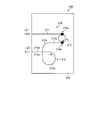
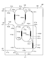
- FIG. 1 is a schematic diagram of an optical waveguide circuit according to the first embodiment.
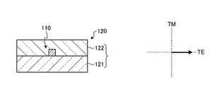
- FIG. 2 is a sectional view of a part of the optical waveguide circuit shown in FIG.
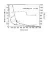
- FIG. 3 is a diagram showing an example of the relationship between the bending radius, the bending loss, and the FSR.
- FIG. 4 is a schematic diagram of the optical waveguide circuit according to the second embodiment.
- FIG. 5 is a schematic diagram of the optical waveguide circuit according to the third embodiment.
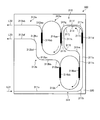
- FIG. 6 is a schematic diagram of the optical waveguide circuit according to the fourth embodiment.
- FIG. 1 is a schematic diagram of an optical waveguide circuit according to the first embodiment.
- the optical waveguide circuit 100 is composed of a PLC (Planar Lightwave Circuit) having an optical waveguide 110 composed of a core and a clad 120.
- PLC Planar Lightwave Circuit
- FIG. 2 is a sectional view of a part of the optical waveguide circuit 100.
- the clad 120 surrounds the optical waveguide 110 and includes a lower clad 121 and an upper clad 122.
- the clad 120 is formed on, for example, a silicon substrate or a glass substrate.
- the clad 120 is made of a quartz glass material.
- the TE polarized wave is a polarized wave parallel to the substrate surface
- the TM polarized wave is a polarized wave perpendicular to the substrate surface.
- the optical waveguide 110 is made of a silica glass material having a refractive index higher than that of the clad 120.
- a silica-based glass material having a high refractive index for example, silica glass containing germania (GeO 2 ) or zirconia (ZrO 2 ) as a dopant for increasing the refractive index can be used.
- SiO 2 —ZrO 2 -based material which is silica glass containing zirconia
- the relative refractive index difference of the optical waveguide 110 with respect to the cladding 120 can be increased to, for example, 4.5% or more, and thus the optical waveguide circuit 100 can be used. It is preferable for downsizing.
- the optical waveguide 110 composed of a core is a buried waveguide filled with a clad 120.
- the relative refractive index difference of the optical waveguide 110 with respect to the clad 120 is 4.5%.
- the optical waveguide 110 includes an input connection waveguide 111, an output connection waveguide 112, a ring-shaped waveguide 113, and an optical multiplexer/demultiplexer 114 that is an optical multiplexer/demultiplexer.
- the ring-shaped waveguide 113 has a circular shape with a constant radius.
- the input connection waveguide 111 includes a plurality of curved waveguides. Specifically, the input connection waveguide 111 includes a straight waveguide 111a, a curved waveguide 111b, a straight waveguide 111c, a curved waveguide 111d, and a straight waveguide 111e. One of the input connection waveguides 111 extends to the side surface of the optical waveguide circuit 100 on the left side of the drawing.
- the output connection waveguide 112 is composed of a straight waveguide. One of the output connection waveguides 112 extends to the side surface on the right side of the drawing of the optical waveguide circuit 100.
- the optical multiplexer/demultiplexer 114 optically connects the ring-shaped waveguide 113 and the input connection waveguide 111, and the ring-shaped waveguide 113 and the output connection waveguide 112.
- the optical multiplexer/demultiplexer 114 is a 2 ⁇ 2 type having two ports on the input side and two ports on the output side, and is, for example, a directional coupling type or multimode optical interference (MMI) type.
- MMI multimode optical interference
- the radius of curvature of the curved waveguide 111b and the curved waveguide 111d is different from the radius of curvature of the ring-shaped waveguide 113.
- the radius of curvature of the curved waveguide 111b and the curved waveguide 111d is 250 ⁇ m.
- the radius of curvature of the ring-shaped waveguide 113 is 206 ⁇ m.
- the light guiding direction is counterclockwise as shown by the arrow, and the curvature sign is negative.
- the bending angle ⁇ 11 of the curved waveguide 111b is 270 degrees.
- the bending angle ⁇ 11 of the curved waveguide 111d is 90 degrees. Therefore, the sum of the products of the curvature sign and the bending angle of the curved waveguides 111b and 111d is -360 degrees.
- the light guiding direction is clockwise as shown by the arrow, and the curvature sign is positive.
- the bending angle of the ring-shaped waveguide 113 is 360 degrees. Therefore, the sum of products of the curvature sign and the bending angle of the ring-shaped waveguide 113 is 360 degrees.
- the sum of the products of the curvature sign and the bending angle of the ring-shaped waveguide 113 is not the sum from the input-side optical multiplexer/demultiplexer to the output-side optical multiplexer/demultiplexer, but the entire ring-shaped waveguide 113 (one round Min) of the curvature code and the bending angle.
- the sum of products of the curvature code and the bending angle of the curved waveguides 111b and 111d and the sum of the products of the curvature code and the bending angle of the ring-shaped waveguide 113 have the same absolute value.
- the signs are opposite.
- the rotation of the polarization plane of light generated in the ring-shaped waveguide 113 and the rotation of the polarization plane of light generated in the curved waveguides 111b and 111d cancel each other out.
- the light L11 input from the input connection waveguide 111 is a single polarization light of TE polarization
- the light L12 output from the output connection waveguide 112 is also a light of TE polarization, and is high.
- the polarization maintaining property is maintained.
- the light L11 is TM-polarized light
- the light L12 is substantially TM-polarized light, and high polarization maintaining property is maintained.
- FIG. 3 is a diagram showing an example of the relationship among the bending radius (Radius), the bending loss (Bending Loss), and the FSR.
- the curvature radii of the curved waveguide 111b and the curved waveguide 111d are different from the curvature radii of the ring-shaped waveguide 113, each can have an optimum value.
- the radius of curvature of the ring-shaped waveguide 113 it is possible to design the FSR to be 150 GHz.
- the optical loss (mainly bending loss) due to the waveguide can be reduced to about 1 dB/cm or less, and the optical waveguide circuit 100 Can be downsized.
- FIG. 3 is a diagram showing an example of the relationship among bending radius (Radius), bending loss (Bending Loss), and FSR.
- the curvature radii of the curved waveguide 111b and the curved waveguide 111d are set to 250 ⁇ m.
- the radius of curvature of the ring-shaped waveguide 113 also needs to be 250 ⁇ m.
- the bending loss can be 1 dB/cm, but the FSR is fixed at 124 GHz.
- the radius of curvature of the ring-shaped waveguide 113 is set to 206 ⁇ m so that the FSR becomes 150 GHz
- the radius of curvature of the curved waveguides 111b and 111d also needs to be 206 ⁇ m.
- the optical loss increases more than when the radius of curvature of the curved waveguides 111b and 111d is 250 ⁇ m, and the bending loss exceeds 1 dB/cm.
- the optical waveguide circuit 100 it is possible to achieve both a high degree of freedom in designing the FSR of the ring-shaped waveguide 113 and a low bending loss while maintaining high polarization retention.
- the above-mentioned radius of curvature and bending angle are examples, and can be freely set according to the requirements of bending loss and FSR.
- the optical waveguide circuit 100 can be manufactured by the following steps, for example. First, fine particles of silica glass are deposited on the substrate by the FHD method, and the fine glass particles are heated into transparent glass to form the lower clad 121. Next, a silica-based glass fine particle layer serving as a core is deposited on the lower clad 121 by a sputtering method. At this time, ZrO 2 is added to SiO 2 so that the refractive index of the silica-based glass fine particle layer serving as the core is higher than that of the cladding so that the relative refractive index difference between the core and the cladding becomes 4.5%.
- an etching mask made of a resist is formed by photolithography using a photomask having the circuit pattern of the optical waveguide 110 of the optical waveguide circuit 100.
- an etching gas such as a fluorine-based gas is used to dry-etch the silica-based glass fine particle layer not covered with the etching mask.
- fine particles of silica glass are deposited by the FHD method, and this is heated to make the glass fine particles into transparent glass to form the upper clad 122 that constitutes the upper part of the clad 120.
- Example 1 an optical waveguide circuit having the configuration of the optical waveguide circuit 100 was manufactured by the above manufacturing method.
- the FSR was 150 GHz.
- TE polarized light was input from the input connection waveguide and the amount of polarization mode coupling was measured, a suitable value of -25 dB or less was obtained.
- the curved waveguide portion of the input connection waveguide was diced and the optical loss was measured, it was a suitable value of 0.95 dB/cm or less.
- an optical waveguide circuit having the same configuration as that of Example 1 was manufactured except that the radius of curvature of each of the two curved waveguides of the input connection waveguide and the ring-shaped waveguide was 250 ⁇ m.
- the amount of wave mode coupling was a suitable value of -25 dB or less, but the FSR was 124 GHz, which was not the desired 150 GHz.
- each of the input connection waveguide and the output connection waveguide is provided with one S-shaped curved waveguide between two straight waveguides, and the S-shaped curved waveguide and the ring-shaped waveguide are provided.
- An optical waveguide circuit having the same configuration as in Example 1 was manufactured except that the curvature radius of each of the waveguides was 250 ⁇ m. In this case, the rotation of the polarization plane of the light generated in each of the input connection waveguide and the output connection waveguide is canceled in the S-shaped curved waveguide.
- the polarization mode coupling amount was -13 dB, which was an unsuitable value for practical use.
- FIG. 4 is a schematic diagram of the optical waveguide circuit according to the second embodiment.
- the optical waveguide circuit 200 is composed of a PLC having an optical waveguide 210 composed of a core and a clad 220.
- the cross-sectional structure of the optical waveguide circuit 200, the materials of the optical waveguide 210 and the clad 220, and the relative refractive index difference may be the same as the corresponding elements of the optical waveguide circuit 100 according to the first embodiment.
- the optical waveguide 210 includes an input connection waveguide 211, an output connection waveguide 212, a ring-shaped waveguide 213, and two optical multiplexers/demultiplexers 214a and 214b forming an optical multiplexer/demultiplexer.
- the ring-shaped waveguide 213 has a circular shape with a constant radius.
- the input connection waveguide 211 is composed of a straight waveguide. One of the input connection waveguides 211 extends to the side surface of the optical waveguide circuit 200 on the left side of the drawing.
- the output connection waveguide 212 includes a plurality of curved waveguides. Specifically, the output connection waveguide 212 includes a straight waveguide 212a, a curved waveguide 212b, a straight waveguide 212c, a curved waveguide 212d, and a straight waveguide 212e.
- One of the output connection waveguides 212 extends to the side surface of the optical waveguide circuit 100 on the left side of the drawing. That is, one of the input connection waveguides 211 and one of the output connection waveguides 212 extend to the same side surface.
- the optical multiplexer/demultiplexer 214a optically connects the ring-shaped waveguide 213 and the input connection waveguide 211.
- the optical multiplexer/demultiplexer 214b optically connects the ring-shaped waveguide 213 and the output connection waveguide 212.
- the optical multiplexer/demultiplexers 214a and 214b are of a 2 ⁇ 2 type, for example, a directional coupling type or an MMI type.
- the radius of curvature of the curved waveguide 212b and the curved waveguide 212d is different from the radius of curvature of the ring-shaped waveguide 213.
- the radius of curvature of the curved waveguide 212b and the curved waveguide 212d is 250 ⁇ m.
- the radius of curvature of the ring-shaped waveguide 213 is 206 ⁇ m.
- the light guiding direction is counterclockwise as indicated by the arrow, and the curvature sign is negative.
- the bending angle of the curved waveguide 212b is 90 degrees.
- the bending angle of the curved waveguide 212d is 270 degrees. Therefore, the sum of the products of the curvature sign and the bending angle of the curved waveguides 212b and 212d is -360 degrees.
- the light guiding direction is clockwise as indicated by the arrow, and the curvature sign is positive.
- the bending angle of the ring-shaped waveguide 213 is 360 degrees. Therefore, the sum of the products of the curvature sign and the bending angle of the ring-shaped waveguide 213 is 360 degrees.
- the sum of products of the curvature code and the bending angle of the curved waveguides 212 b and 212 d and the sum of the products of the curvature code and the bending angle of the ring-shaped waveguide 213 have the same absolute value.
- the signs are opposite.
- the rotation of the polarization plane of light generated in the ring-shaped waveguide 213 and the rotation of the polarization plane of light generated in the curved waveguides 212b and 212d cancel each other out.
- the input light L21 is TE polarized light or TM polarized light
- each can be set to an optimum value.
- the FSR can be designed to be 150 GHz.
- the optical loss mainly bending loss due to the waveguide can be reduced to about 1 dB/cm or less, and the optical waveguide circuit 200 Can be downsized.
- the optical waveguide circuit 200 it is possible to achieve both a high degree of freedom in designing the FSR of the ring-shaped waveguide 213 and low bending loss while maintaining high polarization retention.
- the above-mentioned radius of curvature and bending angle are examples, and can be freely set according to the requirements of bending loss and FSR.
- the optical waveguide circuit 200 since one of the input connection waveguides 211 and one of the output connection waveguides 212 extend to the same side surface, it is easy to connect with the optical fiber array or another optical waveguide circuit.
- Example 2 an optical waveguide circuit having the configuration of the optical waveguide circuit 200 was manufactured by the above manufacturing method.
- the FSR was 150 GHz.
- TE polarized light was input from the input connection waveguide and the amount of polarization mode coupling was measured, a suitable value of -25 dB or less was obtained.
- the curved waveguide portion of the output connection waveguide was diced and the optical loss was measured, it was a suitable value of 0.95 dB/cm or less.
- FIG. 5 is a schematic diagram of the optical waveguide circuit according to the third embodiment.
- the optical waveguide circuit 300 is composed of a PLC having an optical waveguide 310 composed of a core and a clad 320.
- the sectional structure of the optical waveguide circuit 300, the material of the optical waveguide 310 and the clad 320, and the relative refractive index difference may be the same as the corresponding elements of the optical waveguide circuit 100 according to the first embodiment.
- the optical waveguide 310 includes a plurality of input connection waveguides 311, two output connection waveguides 312a and 312b, and two ring-shaped waveguides 313a and 313b in the present embodiment, and an optical multiplexer/demultiplexer.
- the four optical multiplexers/demultiplexers 314aa, 314ab, 314ba, and 314bb are provided.
- the ring-shaped waveguides 313a and 313b are configured to include curved waveguides having a fixed radius and a bending angle of 90 degrees, and are elliptical including the optical multiplexers/demultiplexers 314aa, 314ab, 314ba, and 314bb.
- the waveguide lengths of the ring-shaped waveguides 313a and 313b are equal to each other, and the circulation directions of light are also equal to each other as indicated by arrows.
- the input connection waveguide 311 includes a plurality of curved waveguides and a branch section. Specifically, the input connection waveguide 311 includes a straight waveguide 311a, a curved waveguide 311b, a straight waveguide 311c, a branching portion 311d, a curved waveguide 311e, a straight waveguide 311f, a curved waveguide 311g, and a curved waveguide 311h. , Straight waveguide 311i, curved waveguide 311j, straight waveguide 311k, curved waveguide 311l, curved waveguide 311m, and straight waveguide 311n.
- One of the input connection waveguides 311 extends to the side surface of the optical waveguide circuit 300 on the left side of the drawing.
- the branching unit 311d branches the input connection waveguide 311.
- the curved waveguide 311e, the straight waveguide 311f, and the curved waveguide 311g constitute a first branch path branched from the branch section 311d and optically connected to the ring-shaped waveguide 313a.
- the first branch has two curved waveguides 311e and 311g.
- the curved waveguide 311h, the straight waveguide 311i, the curved waveguide 311j, the straight waveguide 311k, the curved waveguide 311l, the curved waveguide 311m, and the straight waveguide 311n are branched from the branch portion 311d to the ring-shaped waveguide 313b.
- a second branch path that is electrically connected.
- the second branch path has three curved waveguides 311h, 311j, 311l, 311m.
- the branching ratio of light in the branching unit 311d is, for example, 1:1 but is not particularly limited.
- the branching portion 311d is a 1 ⁇ 2 type, for example, a directional coupling type or an MMI type.
- the curved waveguide 311l and the curved waveguide 311m are continuous, but since the signs of their curvatures are different, they can be regarded as separate curved waveguides. In the present specification, even if two curved waveguides are continuous, if the signs of curvature or the radii of curvature differ, they are regarded as separate curved waveguides.
- the output connection waveguide 312a is composed of a curved waveguide 312aa and a straight waveguide 312ab.
- the output connection waveguide 312b includes a curved waveguide 312ba, a straight waveguide 312bb, a curved waveguide 312bc, a straight waveguide 312bd, a curved waveguide 312be, and a straight waveguide 312bf.
- One of the output connection waveguides 312a and 312b extends to the side surface on the left side of the drawing of the optical waveguide circuit 300. That is, one of the input connection waveguides 311 and one of the output connection waveguides 312a and 312b extend to the same side surface.
- the optical multiplexer/demultiplexer 314aa optically connects the ring-shaped waveguide 313a and the curved waveguide 311g forming the first branch in the input connection waveguide 311.
- the optical multiplexer/demultiplexer 314ab optically connects the ring-shaped waveguide 313a and the curved waveguide 312aa of the output connection waveguide 312a.
- the optical multiplexer/demultiplexer 314ba optically connects the ring-shaped waveguide 313b and the straight waveguide 311n forming the second branch in the input connection waveguide 311.
- the optical multiplexer/demultiplexer 314bb optically connects the ring-shaped waveguide 313b and the curved waveguide 312ba of the output connection waveguide 312b.
- the optical multiplexer/demultiplexers 314aa, 314ab, 314ba, 314bb are 2 ⁇ 2 type, for example, directional coupling type or MMI type.
- the curvature radii of the curved waveguides of the input connection waveguide 311 and the output connection waveguides 312a and 312b are different from the curvature radii of the curved waveguides of the ring-shaped waveguides 313a and 313b.
- the curvature radius of each curved waveguide of the input connection waveguide 311 and the output connection waveguides 312a and 312b is 250 ⁇ m.
- the radius of curvature of the curved waveguides of the ring-shaped waveguides 313a and 313b is 412 ⁇ m.
- the light guiding direction is counterclockwise and the curvature sign is negative.
- the bending angles of the curved waveguides 311b, 311e, and 311g are 90 degrees, respectively. Therefore, the sum of the products of the curvature sign and the bending angle of the curved waveguides 311b, 311e, and 311g is -270 degrees.
- the waveguide direction of light is clockwise as shown by the arrow, and the curvature sign is positive.
- the bending angle of the curved waveguide of the ring-shaped waveguide 313a is 360 degrees. Therefore, the sum of products of the curvature sign and the bending angle in the ring-shaped waveguide 313a is 360 degrees.
- the waveguide direction of light is counterclockwise, the curvature sign is negative, and the bending angle is 90 degrees. Therefore, the product of the curvature sign and the bending angle of the curved waveguide 312aa is ⁇ 90 degrees.
- the sum of products of the curvature code and the bending angle of the curved waveguides 311b, 311e, 311g, and 312aa and the sum of the products of the curvature code and the bending angle of the ring-shaped waveguide 313a have the same absolute value.
- the signs are opposite.
- the rotation of the polarization plane of the light generated in the ring-shaped waveguide 313a and the rotation of the polarization plane of the light generated in the curved waveguides 311b, 311e, 311g, and 312aa cancel each other out.
- the input light L31 is TE polarized light or TM polarized light
- the light L32 is output in a state where high polarization maintaining property is maintained.
- the light guiding direction is counterclockwise or clockwise, and The sign is negative or positive.
- the bending angles of the curved waveguides 311b, 311h, 311j, 311l, 311m are 90 degrees, respectively. Therefore, the sum of the products of the curvature sign and the bending angle of the curved waveguides 311b, 311h, 311j, 311l, 311m is -270 degrees.
- the sums of the products of the curvature sign and the bending angle of the curved waveguide in each of the first branch path and the second branch path are equal to each other.
- the waveguide direction of light is clockwise as shown by the arrow, and the curvature sign is positive.
- the bending angle of the curved waveguide of the ring-shaped waveguide 313b is 360 degrees. Therefore, the sum of products of the curvature sign and the bending angle in the ring-shaped waveguide 313b is 360 degrees.
- the light guiding direction is counterclockwise or clockwise
- the curvature sign is negative or positive
- the bending angle is 90 degrees. .. Therefore, the sum of the products of the curvature sign and the bending angle of the curved waveguides 312ba, 312bc, 312be is ⁇ 90 degrees.
- the absolute values are the same and the signs are opposite. Accordingly, the rotation of the polarization plane of the light generated in the ring-shaped waveguide 313b and the rotation of the polarization plane of the light generated in the curved waveguides 311b, 311h, 311j, 311l, 311m, 312ba, 312bc, and 312be cancel each other out. ..
- the input light L31 is TE polarized light or TM polarized light
- the light L33 is output in a state where high polarization maintaining property is maintained.
- the curvature radii of the curved waveguides in the input connection waveguide 311 and the output connection waveguides 312a and 312b are different from the curvature radii of the ring-shaped waveguides 313a and 313b. It can be a value.
- the FSR can be designed to be 75 GHz.
- the optical loss due to the waveguide can be reduced and the optical waveguide circuit 300 can be miniaturized.
- the optical waveguide circuit 200 it is possible to achieve both a high degree of freedom in FSR design and a low bending loss while maintaining a high polarization maintaining property.
- the above-mentioned radius of curvature and bending angle are examples, and can be freely set according to the requirements of bending loss and FSR.
- one of the input connection waveguides 311 and one of the output connection waveguides 312a and 312b extend to the same side face, so that they are connected to the optical fiber array or another optical waveguide circuit. easy.
- an optical waveguide circuit having the configuration of the optical waveguide circuit 300 was manufactured by the above manufacturing method.
- the FSR of the ring resonator including the two ring waveguides was 75 GHz.
- a suitable value of -25 dB or less was obtained.
- the curved waveguide portions of the input connection waveguide and the output connection waveguide were diced and the optical loss was measured, it was a suitable value of 0.95 dB/cm or less.
- FIG. 6 is a schematic diagram of the optical waveguide circuit according to the fourth embodiment.
- the optical waveguide circuit 400 is composed of a PLC having an optical waveguide 410 composed of a core and a clad 420.
- the cross-sectional structure of the optical waveguide circuit 400, the material of the optical waveguide 410 and the clad 420, and the relative refractive index difference may be the same as the corresponding elements of the optical waveguide circuit 100 according to the first embodiment.
- the optical waveguide 410 includes a plurality of input connection waveguides 411, two output connection waveguides 412a and 412b, and two ring-shaped waveguides 413a and 413b in this embodiment, and an optical multiplexer/demultiplexer.
- the four optical multiplexers/demultiplexers 414aa, 414ab, 414ba, 414bb are provided.
- the ring-shaped waveguides 413a and 413b are configured to include curved waveguides having a constant radius and a bending angle of 90 degrees, and are elliptical including the optical multiplexers/demultiplexers 314aa, 314ab, 314ba, and 314bb.
- the ring-shaped waveguide 413b also includes a linear waveguide.
- the waveguide lengths of the ring-shaped waveguides 413a and 413b are different from each other, and the light circulation directions are also different from each other as indicated by arrows.
- the input connection waveguide 411 includes a plurality of curved waveguides and a branch portion. Specifically, the input connection waveguide 411 includes the straight waveguide 411a, the curved waveguide 411b, the curved waveguide 411c, the straight waveguide 411d, the curved waveguide 411e, the branching portion 411f, the straight waveguide 411g, and the curved waveguide 411h. , Straight waveguide 411i, curved waveguide 411j, straight waveguide 411k, straight waveguide 411l, straight waveguide 411m, straight waveguide 411n.
- One of the input connection waveguides 411 extends to the side surface on the left side of the drawing of the optical waveguide circuit 400.
- the branching unit 411f branches the input connection waveguide 411.
- the straight waveguide 411g, the curved waveguide 411h, the straight waveguide 411i, and the curved waveguide 411j constitute a first branch that is branched from the branch portion 411f and is optically connected to the ring-shaped waveguide 413a.
- the first branch path has two curved waveguides 411h and 411j.
- the straight waveguide 411k, the curved waveguide 411l, the curved waveguide 411m, and the straight waveguide 411n constitute a second branch path branched from the branch portion 411f and optically connected to the ring-shaped waveguide 413b.
- the second branch has two curved waveguides 411l and 411m.
- the branching ratio of light in the branching section 411f is, for example, 1:1 but is not particularly limited.
- the branching portion 411f is a 1 ⁇ 2 type, for example, a directional coupling type or an MMI type
- the output connection waveguide 412a is composed of a curved waveguide 412aa and a straight waveguide 412ab.
- the output connection waveguide 412b is a curved waveguide 412ba, a straight waveguide 412bb, a curved waveguide 412bc, a straight waveguide 412bd, a curved waveguide 412be, a straight waveguide 412bf, a curved waveguide 412bg, a straight waveguide 412bh, a curved waveguide. 412bi, a straight waveguide 412bj, a curved waveguide 412bk, and a straight waveguide 412bl.
- One of the output connection waveguides 412a and 412b extends to the side surface on the left side of the drawing of the optical waveguide circuit 400. That is, one of the input connection waveguides 411 and one of the output connection waveguides 412a and 412b extend to the same side surface.
- the optical multiplexer/demultiplexer 414aa optically connects the ring-shaped waveguide 413a and the curved waveguide 411j forming the first branch in the input connection waveguide 411.
- the optical multiplexer/demultiplexer 414ab optically connects the ring-shaped waveguide 413a and the curved waveguide 412aa of the output connection waveguide 412a.
- the optical multiplexer/demultiplexer 414ba optically connects the ring-shaped waveguide 413b and the linear waveguide 411n forming the second branch in the input connection waveguide 411.
- the optical multiplexer/demultiplexer 414bb optically connects the ring-shaped waveguide 413b and the curved waveguide 412ba of the output connection waveguide 412b.
- the optical multiplexer/demultiplexers 414aa, 414ab, 414ba, 414bb are 2 ⁇ 2 type, for example, directional coupling type or MMI type.
- the curvature radii of the curved waveguides of the input connection waveguide 411 and the output connection waveguides 412a, 412b are different from the curvature radii of the curved waveguides of the ring-shaped waveguides 413a, 413b.
- the radius of curvature of each curved waveguide of the input connection waveguide 411 and the output connection waveguides 412a and 412b is 250 ⁇ m.
- the radius of curvature of the curved waveguides of the ring-shaped waveguides 413a and 413b is 412 ⁇ m.
- the length of the straight waveguide of the ring-shaped waveguide 413b is 1244 ⁇ m.
- the light guiding direction is counterclockwise or counterclockwise.
- the curvature sign is negative or positive, and the bending angle is 60 degrees or 90 degrees.
- the sum of products of the curvature sign and the bending angle of the curved waveguides 411b, 411c, 411e, 411h, 411j is -270 degrees.
- the light guiding direction is clockwise as indicated by the arrow, and the curvature sign is positive.
- the bending angle of the curved waveguide of the ring-shaped waveguide 413a is 360 degrees. Therefore, the sum of products of the curvature sign and the bending angle in the ring-shaped waveguide 413a is 360 degrees.
- the waveguide direction of light is counterclockwise, the curvature sign is negative, and the bending angle is 90 degrees. Therefore, the product of the curvature sign and the bending angle of the curved waveguide 412aa is ⁇ 90 degrees.
- the sum of the products of the curvature code and the bending angle of the curved waveguides 411b, 411c, 411e, 411h, 411j, and 412aa and the sum of the products of the curvature code and the bending angle of the ring-shaped waveguide 413a are absolute.
- the values are the same, but the signs are opposite. This cancels the rotation of the polarization plane of the light generated in the ring-shaped waveguide 413a and the rotation of the polarization plane of the light generated in the curved waveguides 411b, 411c, 411e, 411h, 411j, and 412aa.
- the input light L41 is TE polarized light or TM polarized light
- the light L42 is output in a state where high polarization maintaining property is maintained.
- the light guiding direction is counterclockwise or clockwise, and The sign is negative or positive, and the bending angle is 60 degrees or 90 degrees.
- the sum of the products of the curvature sign and the bending angle of the curved waveguides 411b, 411c, 411e, 411l, 411m is -90 degrees.
- the sums of the products of the curvature sign and the bending angle of the curved waveguides in the first branch path and the second branch path are different from each other.
- the light guiding direction is counterclockwise as shown by the arrow, and the curvature sign is negative.
- the bending angle of the curved waveguide of the ring-shaped waveguide 413b is 360 degrees. Therefore, the sum of products of the curvature sign and the bending angle in the ring-shaped waveguide 413b is ⁇ 360 degrees.
- the light guiding direction is counterclockwise or clockwise, and the curvature sign is negative or positive,
- the bending angle is 90 degrees or 180 degrees.
- the sum of the products of the curvature sign and the bending angle of the curved waveguides 412ba, 412bc, 412be, 412bg, 412bi, 412bk is 450 degrees.
- the sum of the products ( ⁇ 90+450 360) of the curvature code and the bending angle of the curved waveguides 411b, 411c, 411e, 411l, 411m, 412ba, 412bc, 412be, 412bg, 412bi, and 412bk, and the ring-shaped waveguide 413b.
- the sum of products of the curvature sign and the bending angle at is the same in absolute value but opposite in sign.
- the rotation of the polarization plane of the light generated in the ring-shaped waveguide 413b and the polarization plane of the light generated in the curved waveguides 411b, 411c, 411e, 411l, 411m, 412ba, 412bc, 412be, 412bg, 412bi, and 412bk The rotation of and cancel each other out.
- the input light L41 is TE polarized light or TM polarized light
- the light L43 is output in a state where high polarization maintaining property is maintained.
- the curvature radii of the curved waveguides in the input connection waveguide 411 and the output connection waveguides 412a, 412b are different from the curvature radii of the ring-shaped waveguides 413a, 413b. It can be a value. Furthermore, since the waveguide lengths of the ring-shaped waveguides 413a and 413b are different from each other, different FSRs can be obtained. For example, the FSR of the ring waveguide 413a can be designed to be 75 GHz, and the FSR of the ring waveguide 413b can be designed to be 50 GHz.
- each curved waveguide in the input connection waveguide 411 and the output connection waveguides 412a and 412b is set to 250 ⁇ m, it is possible to reduce the optical loss due to the waveguide and to downsize the optical waveguide circuit 400. Further, in the optical waveguide circuit 400, since the light circulation directions of the ring-shaped waveguides 413a and 413b can be made opposite to each other, the degree of freedom in design is high.
- the optical waveguide circuit 400 it is possible to achieve both a high degree of freedom in FSR design and a low bending loss while maintaining high polarization retention.
- the above-mentioned radius of curvature and bending angle are merely examples, and can be freely set according to the requirements of bending loss and FSR.
- one of the input connection waveguides 411 and one of the output connection waveguides 412a and 412b extend to the same side face, so that they are connected to the optical fiber array or another optical waveguide circuit. easy.
- Example 4 an optical waveguide circuit having the configuration of the optical waveguide circuit 400 was manufactured by the above manufacturing method.
- the FSR of the ring resonator including the two ring-shaped waveguides was 75 GHz and 50.2 GHz.
- TE polarized light was input from the input connection waveguide and the amount of polarization mode coupling was measured, a suitable value of -25 dB or less was obtained.
- the curved waveguide portions of the input connection waveguide and the output connection waveguide were diced and the optical loss was measured, it was a suitable value of 0.95 dB/cm or less.
- the present invention is not limited to the above embodiment.
- the number of ring-shaped waveguides may be 3 or more
- the number of branch portions may be 2 or more
- the number of branch paths may be 3 or more.
- the present invention also includes those configured by appropriately combining the above-described components. Further, further effects and modified examples can be easily derived by those skilled in the art. Therefore, the broader aspects of the present invention are not limited to the above embodiments, and various modifications can be made.
- the present invention can be applied to an optical waveguide circuit.
- Optical waveguide circuit 110 210, 310, 410 Optical waveguide 111, 211, 311, 411 Input connection waveguide 111a, 111c, 111e, 212a, 212c, 212e, 311a, 311c, 311f, 311i, 311k, 311n, 312ab, 312bb, 312bd, 312bf, 411a, 411d, 411g, 411i, 411k, 411n, 412ab, 412bb, 412bd, 412bf, 412bh, 412bj, 412bl linear waveguides 111b, 111d, 212b, 212d, 311b.
Landscapes
- Physics & Mathematics (AREA)
- Engineering & Computer Science (AREA)
- Microelectronics & Electronic Packaging (AREA)
- General Physics & Mathematics (AREA)
- Optics & Photonics (AREA)
- Optical Integrated Circuits (AREA)
Abstract
光導波路回路は、リング状導波路と、入力接続導波路と、出力接続導波路と、前記リング状導波路と前記入力接続導波路、および前記リング状導波路と前記出力接続導波路とを光学的に接続する光合分波部と、を備え、前記入力接続導波路および前記出力接続導波路の少なくともいずれか一方は、複数の曲線導波路を含み、前記複数の曲線導波路の曲率符号と屈曲角度との積の総和と、前記リング状導波路の曲率符号と屈曲角度との積の総和は、絶対値が同じで符号が反対であり、前記リング状導波路において発生した光の偏波面の回転と、前記複数の曲線導波路において発生した光の偏波面の回転とが打ち消し合う。
Description
本発明は、リング状導波路を備える光導波路回路に関するものである。
光通信で用いられ、リング状導波路を有し、入力光の偏波状態を保持して出力する光導波回路が知られている。この種の光導波路回路は、リング状導波路、光合分波器、入力接続導波路、出力接続導波路から構成される。リング状導波路は円弧状の曲線導波路からなる。この種の光導波路回路の光透過強度は周期的な間隔(FSR: Free Spectral Range)もつ波長依存性を示す。FSRは、光速c、リング状導波路の導波路長L、リング状導波路の実効屈折率nを用いて、FSR=c/nLと表される。リング状導波路長を調整すれば自在にFSRを設定できる。光通信には様々な透過特性をもつ光フィルタが使用されており、その一部はリング共振器を適用して実現することが可能である。
近年の光通信技術には偏波多重信号が用いられており、光導波路回路には入力した偏波を維持したまま出力する特性(偏波保持性と呼ぶ)が求められる。しかしながら、実際の光導波路回路では下記の理由で偏波保持性が失われていることがある。
基板上に形成された光導波路には導波路断面に対し非等方的な応力が存在する。これは、基板面に水平方向にはクラッドとコアからなる構造が平面状に広がっているが、基板面に垂直方向には一般的に水平方向よりも薄い構造となっており、それぞれの方向に対して導波路にかかる応力が異なるためである。また、導波路を構成する基板、下部クラッド、コア、上部クラッドの熱膨張係数が異なるとき、導波路の作製工程にて例えば1000℃以上の高温熱処理があると、その冷却過程で導波路に熱応力が発生する。さらに上部クラッドの製法がFHD(Flame Hydrolysis Deposition)法である場合、微粒子からなる多孔質体を堆積し透明ガラス化させる過程でその体積が大きく変化し場合によってはコアを変形させるほどの大きな応力が発生する。これらの応力は異方性をもち、各偏波モードの振動面(振動方向を偏波主軸、振動面を偏波面と呼ぶ)が基板面に対して傾く原因となる。これは入力された偏波を維持して出力するといった偏波保持性を要求される光導波路回路において課題となる。
したがって、光導波路回路に、TE(Transverse Electric)偏波(基板面と平行方向の偏波)の光を入力した際に、TM(Transverse Magnetic)偏波の光が発生する場合がある。ここでTM偏波とは基板面と垂直方向の偏波を指す。つまり入力時で存在しなかったTM偏波の光が発生し、TE偏波の光の強度は減少する。この現象は、偏波結合と呼び、この場合TM成分強度をTE偏波成分強度で割った偏波モード結合量で示すことが出来る。偏波を維持する用途において、偏波保持性が高いほど好ましい。つまり、偏波モード結合量が小さいほど好ましく、一般的に-20dB以下が望まれる。
特許文献1には、曲率の正負が逆で曲率半径が等しく、かつ弧の角度が等しい屈曲部を組み合わせ、屈曲部で発生する光の偏波面の回転を打ち消しあう技術が開示されている。
しかしながら、高い偏波保持性を実現するために、リング状導波路、光合分波器、入力接続導波路、出力接続導波路を備える光導波路回路において、曲率の正負が逆で曲率半径が等しく、かつ弧の角度が等しい屈曲部を組み合わせると、以下の問題が生じる。すなわち、屈曲部の特性として、曲率の正負、曲率半径、弧の角度の組み合わせが限定されてしまうため、リング共振器のFSRを自由に設計できない可能性がある。一方、リング共振器のFSRを所望の値とするために屈曲部の特性を決定すると、それに応じて入力接続導波路、出力接続導波路に屈曲部を設ける必要があるが、屈曲部に過度の曲げ損失が生じる可能性がある。
本発明は、上記に鑑みてなされたものであって、高い偏波保持性を維持しながら、リング共振器のFSRの設計の自由度の高さと低い曲げ損失との両立を実現できる光導波路回路を提供することを目的とする。
上述した課題を解決し、目的を達成するために、本発明の一態様に係る光導波路回路は、リング状導波路と、入力接続導波路と、出力接続導波路と、前記リング状導波路と前記入力接続導波路、および前記リング状導波路と前記出力接続導波路とを光学的に接続する光合分波部と、を備え、前記入力接続導波路および前記出力接続導波路の少なくともいずれか一方は、複数の曲線導波路を含み、前記複数の曲線導波路の曲率符号と屈曲角度との積の総和と、前記リング状導波路の曲率符号と屈曲角度との積の総和は、絶対値が同じで符号が反対であり、前記リング状導波路において発生した光の偏波面の回転と、前記複数の曲線導波路において発生した光の偏波面の回転とが打ち消し合うことを特徴とする。
本発明の一態様に係る光導波路回路は、前記複数の曲線導波路の曲率半径と、前記リング状導波路の曲率半径とが異なっていることを特徴とする。
本発明の一態様に係る光導波路回路は、前記複数の曲線導波路の曲率符号と屈曲角度との積の総和の絶対値は、360度であることを特徴とする。
本発明の一態様に係る光導波路回路は、前記複数の曲線導波路のそれぞれは、導波による光損失が1.0dB/cm以下となる曲率半径であることを特徴とする。
本発明の一態様に係る光導波路回路は、前記光合分波部は、2つの光合分波器を有し、前記入力接続導波路の一方と、前記出力接続導波路の一方とが、同一の側面へ延びていることを特徴とする。
本発明の一態様に係る光導波路回路は、複数の前記リング状導波路を備え、前記入力接続導波路は、少なくとも1つの分岐部と、前記少なくとも1つの分岐部から分岐されて前記複数のリング状導波路のそれぞれに光学的に接続する複数の分岐路とを有し、前記複数の分岐路は、前記複数の曲線導波路を2箇所以上有し、前記分岐路のそれぞれにおける曲線導波路の曲率符号と屈曲角度との積の総和が、互いに等しいことを特徴とする。
本発明の一態様に係る光導波路回路は、複数の前記リング状導波路を備え、前記入力接続導波路は、少なくとも1つの分岐部と、前記少なくとも1つの分岐部から分岐されて前記複数のリング状導波路のそれぞれに光学的に接続する複数の分岐路とを有し、前記複数の分岐路は、前記複数の曲線導波路を2箇所以上有し、前記複数のリング状導波路は、光の周回方向が互いに異なるリング状導波路を含むことを特徴とする。
本発明の一態様に係る光導波路回路は、前記分岐路のそれぞれにおける曲線導波路の曲率符号と屈曲角度との積の総和が、互いに異なることを特徴とする。
本発明の一態様に係る光導波路回路は、複数の前記リング状導波路を備え、前記複数のリング状導波路は、導波路長が互いに異なるリング状導波路を含むことを特徴とする。
本発明の一態様に係る光導波路回路は、前記入力接続導波路からTE偏波またはTM偏波の単一偏波の光を入力した場合、前記出力接続導波路から出力された光における偏波モード結合量が-25dB以下であることを特徴とする。
本発明の一態様に係る光導波路回路は、前記入力接続導波路、前記リング状導波路、前記出力接続導波路、および前記光合分波部はコアによって構成され、前記コアはクラッドによって埋め込まれた埋め込み導波路であることを特徴とする。
本発明の一態様に係る光導波路回路は、前記クラッドに対する前記コアの比屈折率差が4.5%以上であることを特徴とする。
本発明の一態様に係る光導波路回路は、前記コアはZrO2を含むことを特徴とする。
本発明によれば、高い偏波保持性を維持しながら、リング共振器のFSRの設計の自由度の高さと低い曲げ損失との両立を実現できるという効果を奏する。
以下に、図面を参照して実施形態について説明する。なお、この実施形態によりこの発明が限定されるものではない。また、図面の記載において、同一または対応する要素には適宜同一の符号を付している。また、図面は模式的なものであり、各要素の寸法の関係、各要素の比率などは、現実と異なる場合があることに留意する必要がある。図面の相互間においても、互いの寸法の関係や比率が異なる部分が含まれている場合がある。
(実施形態1)
図1は、実施形態1に係る光導波路回路の模式図である。光導波路回路100は、コアで構成されている光導波路110とクラッド120とを有するPLC(Planar Lightwave Circuit)で構成されている。
図1は、実施形態1に係る光導波路回路の模式図である。光導波路回路100は、コアで構成されている光導波路110とクラッド120とを有するPLC(Planar Lightwave Circuit)で構成されている。
図2は、光導波路回路100の一部の断面図である。クラッド120は、光導波路110を取り囲んでおり、下部クラッド121と、上部クラッド122とを備えている。クラッド120は、例えばシリコン基板やガラス基板上に形成されている。クラッド120は、石英系ガラス材料で構成されている。なお、図示するように、TE偏波は基板面と平行方向の偏波であり、TM偏波は基板面と垂直方向の偏波である。
光導波路110は、クラッド120の屈折率よりも高い屈折率を有する石英系ガラス材料で構成されている。このような屈折率が高い石英系ガラス材料として、たとえば屈折率を高めるドーパントとしてのゲルマニア(GeO2)やジルコニア(ZrO2)を含む石英ガラスを用いることができる。特に、ジルコニアを含む石英ガラスであるいわゆるSiO2-ZrO2系材料であれば、クラッド120に対する光導波路110の比屈折率差を、たとえば4.5%以上と高くできるので、光導波路回路100を小型化する場合には好ましい。コアで構成されている光導波路110はクラッド120によって埋め込まれた埋め込み導波路である。
本実施形態では、クラッド120に対する光導波路110の比屈折率差が4.5%であるとする。
図1に戻って、光導波路110は、入力接続導波路111と、出力接続導波路112と、リング状導波路113と、光合分波部である光合分波器114とを備えている。
リング状導波路113は、一定の半径を有する円状である。入力接続導波路111は、複数の曲線導波路を含む。具体的には、入力接続導波路111は、直線導波路111a、曲線導波路111b、直線導波路111c、曲線導波路111d、直線導波路111e、とで構成されている。入力接続導波路111の一方は光導波路回路100の図面左側の側面へ延びている。
出力接続導波路112は、直線導波路で構成されている。出力接続導波路112の一方は、光導波路回路100の図面右側の側面へ延びている。
光合分波器114は、リング状導波路113と入力接続導波路111、およびリング状導波路113と出力接続導波路112とを光学的に接続する。光合分波器114は、入力側が2ポート、出力側が2ポートの2×2型であり、たとえば方向性結合型や多モード光干渉(MMI)型のものである。
曲線導波路111b、曲線導波路111dの曲率半径と、リング状導波路113の曲率半径とは異なっている。例えば、曲線導波路111b、曲線導波路111dの曲率半径は250μmである。リング状導波路113の曲率半径は206μmである。
また、曲線導波路111b、曲線導波路111dは、光の導波方向が矢印で示すように反時計回りであり、曲率符号が負である。曲線導波路111bの屈曲角度θ11は270度である。曲線導波路111dの屈曲角度θ11は90度である。したがって、曲線導波路111b、曲線導波路111dの曲率符号と屈曲角度との積の総和は-360度である。
一方、リング状導波路113は、光の導波方向が矢印で示すように時計回りであり、曲率符号が正である。リング状導波路113の屈曲角度は360度である。したがって、リング状導波路113の曲率符号と屈曲角度との積の総和は360度である。なお、リング状導波路113の曲率符号と屈曲角度との積の総和は、入力側の光合分波部から出力側の光合分波部までの総和でなく、リング状導波路113の全体(一周分)の曲率符号と屈曲角度との積の総和であるものとする。
このように、曲線導波路111b、曲線導波路111dの曲率符号と屈曲角度との積の総和と、リング状導波路113の曲率符号と屈曲角度との積の総和とが、絶対値が同じで符号が反対となっている。これによって、リング状導波路113において発生した光の偏波面の回転と、曲線導波路111b、曲線導波路111dにおいて発生した光の偏波面の回転とが打ち消し合う。
したがって、入力接続導波路111から入力される光L11がTE偏波の単一偏波の光であるとすると、出力接続導波路112から出力される光L12も略TE偏波の光となり、高い偏波保持性が維持される。同様に、光L11がTM偏波の光の場合も光L12が略TM偏波の光となり、高い偏波保持性が維持される。
また、図3は、曲げ半径(Radius)と曲げ損失(Bending Loss)およびFSRとの関係の一例を示す図である。光導波路回路100では、曲線導波路111b、曲線導波路111dの曲率半径と、リング状導波路113の曲率半径とは異なっているので、それぞれを最適な値とできる。たとえば、リング状導波路113の曲率半径を206μmとすることで、FSRを150GHzとなるように設計できる。また、曲線導波路111b、曲線導波路111dの曲率半径を250μmとすることで、導波による光損失(主には曲げ損失)を1dB/cm程度またはそれ以下に低減でき、かつ光導波路回路100を小型化できる。
たとえば、図3は、曲げ半径(Radius)と曲げ損失(Bending Loss)およびFSRとの関係の一例を示す図である。
特許文献1のように、曲率の正負が逆で曲率半径が等しく、かつ弧の角度が等しい屈曲部を組み合わせた技術の場合は、曲線導波路111b、曲線導波路111dの曲率半径を250μmとした場合は、リング状導波路113の曲率半径も250μmとする必要がある。この場合、曲げ損失を1dB/cmとできるが、FSRは124GHzに固定されてしまう。一方、FSRを150GHzとなるようにリング状導波路113の曲率半径を206μmとすると、曲線導波路111b、曲線導波路111dの曲率半径も206μmとする必要がある。この場合、曲線導波路111b、曲線導波路111dの曲率半径を250μmとした場合よりも光損失が増加してしまい、曲げ損失が1dB/cmを超えてしまう。
以上説明したように、光導波路回路100では、高い偏波保持性を維持しながら、リング状導波路113のFSRの設計の自由度の高さと低い曲げ損失との両立を実現できる。なお、上記の曲率半径や屈曲角度は例示であって、曲げ損失やFSRの要求に応じて自由に設定できる。
光導波路回路100は、たとえば以下のような工程で製造できる。まず、FHD法により、基板上に石英系ガラスの微粒子を堆積し、これを加熱してガラス微粒子を透明ガラス化し、下部クラッド121を形成する。つぎに、下部クラッド121上にスパッタ法によって、コアとなる石英系ガラス微粒子層を堆積する。この際、コアとクラッドの比屈折率差が4.5%となるように、ZrO2をSiO2に添加してコアとなる石英系ガラス微粒子層の屈折率をクラッドよりも高くする。つぎに、光導波路回路100の光導波路110の回路パターンをもつフォトマスクを使ったフォトリソグラフィにより、レジストからなるエッチングマスクを形成する。続いて、フッ素系ガスなどのエッチングガスを用いて、エッチングマスクで覆われていない石英系ガラス微粒子層のドライエッチングを行う。最後に、FHD法により石英系ガラスの微粒子を堆積し、これを加熱してガラス微粒子を透明ガラス化し、クラッド120の上部を構成する上部クラッド122を形成する。以上により、光導波路回路100を製造できる。
実施例1として、上記製造方法にて光導波路回路100の構成を有する光導波路回路を製造した。製造した光導波路回路の特性を測定したところ、FSRは150GHzであった。また、入力接続導波路からTE偏波の光を入力して、その偏波モード結合量を測定したところ、-25dB以下の好適な値が得られた。また、入力接続導波路の曲線導波路部をダイシングしてその光損失を測定したところ、0.95dB/cm以下の好適な値であった。
なお、比較例1として、入力接続導波路の2つの曲線導波路とリング状導波路とのいずれの曲率半径も250μmとした以外は実施例1と同じ構成の光導波路回路を製造したところ、偏波モード結合量が-25dB以下の好適な値であったが、FSRは124GHzであり、所望の150GHzとはできなかった。
また、比較例2として、入力接続導波路と出力接続導波路とのそれぞれを、2つの直線導波路の間に1つのS字の曲線導波路を設け、S字の曲線導波路とリング状導波路とのいずれの曲率半径も250μmとした以外は実施例1と同じ構成の光導波路回路を製造した。この場合、入力接続導波路と出力接続導波路とのそれぞれにおいて発生した光の偏波面の回転は、S字の曲線導波路内で打ち消させる。しかしながら、光導波路回路の特性を測定したところ、偏波モード結合量が-13dBとなり、実用上不適当な値であった。
(実施形態2)
図4は、実施形態2に係る光導波路回路の模式図である。光導波路回路200は、コアで構成されている光導波路210とクラッド220とを有するPLCで構成されている。
図4は、実施形態2に係る光導波路回路の模式図である。光導波路回路200は、コアで構成されている光導波路210とクラッド220とを有するPLCで構成されている。
光導波路回路200の断面構造や、光導波路210やクラッド220の材料や比屈折率差は、実施形態1に係る光導波路回路100の対応する要素と同じであってよい。
光導波路210は、入力接続導波路211と、出力接続導波路212と、リング状導波路213と、光合分波部を構成する2つの光合分波器214a、214bとを備えている。
リング状導波路213は、一定の半径を有する円状である。入力接続導波路211は、直線導波路で構成されている。入力接続導波路211の一方は、光導波路回路200の図面左側の側面へ延びている。
出力接続導波路212は、複数の曲線導波路を含む。具体的には、出力接続導波路212は、直線導波路212a、曲線導波路212b、直線導波路212c、曲線導波路212d、直線導波路212e、とで構成されている。出力接続導波路212の一方は光導波路回路100の図面左側の側面へ延びている。すなわち、入力接続導波路211の一方と、出力接続導波路212の一方とが、同一の側面へ延びている。
光合分波器214aは、リング状導波路213と入力接続導波路211とを光学的に接続する。光合分波器214bは、リング状導波路213と出力接続導波路212とを光学的に接続する。光合分波器214a、214bは、2×2型であり、たとえば方向性結合型やMMI型のものである。
曲線導波路212b、曲線導波路212dの曲率半径と、リング状導波路213の曲率半径とは異なっている。例えば、曲線導波路212b、曲線導波路212dの曲率半径は250μmである。リング状導波路213の曲率半径は206μmである。
また、曲線導波路212b、曲線導波路212dは、光の導波方向が矢印で示すように反時計回りであり、曲率符号が負である。曲線導波路212bの屈曲角度は90度である。曲線導波路212dの屈曲角度は270度である。したがって、曲線導波路212b、曲線導波路212dの曲率符号と屈曲角度との積の総和は-360度である。
一方、リング状導波路213は、光の導波方向が矢印で示すように時計回りであり、曲率符号が正である。リング状導波路213の屈曲角度は360度である。したがって、リング状導波路213の曲率符号と屈曲角度との積の総和は360度である。
このように、曲線導波路212b、曲線導波路212dの曲率符号と屈曲角度との積の総和と、リング状導波路213の曲率符号と屈曲角度との積の総和とが、絶対値が同じで符号が反対となっている。これによって、リング状導波路213において発生した光の偏波面の回転と、曲線導波路212b、曲線導波路212dにおいて発生した光の偏波面の回転とが打ち消し合う。その結果、入力された光L21がTE偏波、TM偏波のいずれにであっても、高い偏波保持性が維持された状態で、光L22が出力される。
光導波路回路200では、曲線導波路212b、曲線導波路212dの曲率半径と、リング状導波路213の曲率半径とは異なっているので、それぞれを最適な値とできる。たとえば、リング状導波路213の曲率半径を206μmとすることで、FSRを150GHzとなるように設計できる。また、曲線導波路212b、曲線導波路212dの曲率半径を250μmとすることで、導波による光損失(主には曲げ損失)を1dB/cm程度またはそれ以下に低減でき、かつ光導波路回路200を小型化できる。
以上説明したように、光導波路回路200では、高い偏波保持性を維持しながら、リング状導波路213のFSRの設計の自由度の高さと低い曲げ損失との両立を実現できる。なお、上記の曲率半径や屈曲角度は例示であって、曲げ損失やFSRの要求に応じて自由に設定できる。また、光導波路回路200では、入力接続導波路211の一方と、出力接続導波路212の一方とが、同一の側面へ延びているので、光ファイバアレイや他の光導波路回路と接続し易い。
実施例2として、上記製造方法にて光導波路回路200の構成を有する光導波路回路を製造した。製造した光導波路回路の特性を測定したところ、FSRは150GHzであった。また、入力接続導波路からTE偏波の光を入力して、その偏波モード結合量を測定したところ、-25dB以下の好適な値が得られた。また、出力接続導波路の曲線導波路部をダイシングしてその光損失を測定したところ、0.95dB/cm以下の好適な値であった。
(実施形態3)
図5は、実施形態3に係る光導波路回路の模式図である。光導波路回路300は、コアで構成されている光導波路310とクラッド320とを有するPLCで構成されている。
図5は、実施形態3に係る光導波路回路の模式図である。光導波路回路300は、コアで構成されている光導波路310とクラッド320とを有するPLCで構成されている。
光導波路回路300の断面構造や、光導波路310やクラッド320の材料や比屈折率差は、実施形態1に係る光導波路回路100の対応する要素と同じであってよい。
光導波路310は、入力接続導波路311と、2つの出力接続導波路312a、312bと、複数であり、本実施形態では2つであるリング状導波路313a、313bと、光合分波部を構成する4つの光合分波器314aa、314ab、314ba、314bbとを備えている。
リング状導波路313a、313bは、一定の半径を有する屈曲角度90度の曲線導波路を含んで構成されており、光合分波器314aa、314ab、314ba、314bbも含めて長円状である。リング状導波路313a、313bのそれぞれの導波路長は互いに等しく、また光の周回方向も矢印で示すように互いに等しい。
入力接続導波路311は、複数の曲線導波路と分岐部とを含む。具体的には、入力接続導波路311は、直線導波路311a、曲線導波路311b、直線導波路311c、分岐部311d、曲線導波路311e、直線導波路311f、曲線導波路311g、曲線導波路311h、直線導波路311i、曲線導波路311j、直線導波路311k、曲線導波路311l、曲線導波路311m、直線導波路311nとで構成されている。入力接続導波路311の一方は光導波路回路300の図面左側の側面へ延びている。分岐部311dは、入力接続導波路311を分岐する。曲線導波路311e、直線導波路311f、曲線導波路311gは、分岐部311dから分岐されてリング状導波路313aに光学的に接続する第1分岐路を構成している。第1分岐路は2箇所の曲線導波路311e、311gを有する。曲線導波路311h、直線導波路311i、曲線導波路311j、直線導波路311k、曲線導波路311l、曲線導波路311m、直線導波路311nは、分岐部311dから分岐されてリング状導波路313bに光学的に接続する第2分岐路を構成している。第2分岐路は3箇所の曲線導波路311h、311j、311l、311mを有する。分岐部311dにおける光の分岐比は、たとえば1:1であるが、特に限定はされない。また、分岐部311dは1×2型であり、たとえば方向性結合型やMMI型のものである。
ここで、曲線導波路311l、曲線導波路311mは、連続しているが、その曲率の符号が異なるので、別個の曲線導波路とみなせる。なお、本明細書においては、2つの曲線導波路が連続していても、曲率の符号または曲率半径が異なれば、別個の曲線導波路とみなす。
出力接続導波路312aは、曲線導波路312aa、直線導波路312ab、とで構成されている。出力接続導波路312bは、曲線導波路312ba、直線導波路312bb、曲線導波路312bc、直線導波路312bd、曲線導波路312be、直線導波路312bf、とで構成されている。出力接続導波路312a、312bの一方は光導波路回路300の図面左側の側面へ延びている。すなわち、入力接続導波路311の一方と出力接続導波路312a、312bの一方とが、同一の側面へ延びている。
光合分波器314aaは、リング状導波路313aと入力接続導波路311において第1分岐路を構成する曲線導波路311gとを光学的に接続する。光合分波器314abは、リング状導波路313aと出力接続導波路312aの曲線導波路312aaとを光学的に接続する。光合分波器314baは、リング状導波路313bと入力接続導波路311において第2分岐路を構成する直線導波路311nとを光学的に接続する。光合分波器314bbは、リング状導波路313bと出力接続導波路312bの曲線導波路312baとを光学的に接続する。光合分波器314aa、314ab、314ba、314bbは、2×2型であり、たとえば方向性結合型やMMI型のものである。
入力接続導波路311、出力接続導波路312a、312bの各曲線導波路の曲率半径と、リング状導波路313a、313bの曲線導波路の曲率半径とは異なっている。例えば、入力接続導波路311、出力接続導波路312a、312bの各曲線導波路の曲率半径は250μmである。リング状導波路313a、313bの曲線導波路の曲率半径は412μmである。
ここで、入力接続導波路311においてリング状導波路313aに到るまでの曲線導波路311b、311e、311gについては、光の導波方向が反時計回りであり、曲率符号が負である。曲線導波路311b、311e、311gの屈曲角度はそれぞれ90度である。したがって、曲線導波路311b、311e、311gの曲率符号と屈曲角度との積の総和は-270度である。
一方、リング状導波路313aの曲線導波路は、光の導波方向が矢印で示すように時計回りであり、曲率符号が正である。リング状導波路313aの曲線導波路の屈曲角度は360度である。したがって、リング状導波路313aにおける曲率符号と屈曲角度との積の総和は360度である。
さらに、出力接続導波路312aにおける曲線導波路312aaについては、光の導波方向が反時計回りであり、曲率符号が負であり、屈曲角度は90度である。したがって、曲線導波路312aaの曲率符号と屈曲角度との積は-90度である。
その結果、曲線導波路311b、311e、311g、312aaの曲率符号と屈曲角度との積の総和と、リング状導波路313aの曲率符号と屈曲角度との積の総和とが、絶対値が同じで符号が反対となっている。これによって、リング状導波路313aにおいて発生した光の偏波面の回転と、曲線導波路311b、311e、311g、312aaにおいて発生した光の偏波面の回転とが打ち消し合う。その結果、入力された光L31がTE偏波、TM偏波のいずれにであっても、高い偏波保持性が維持された状態で、光L32が出力される。
同様に、入力接続導波路311においてリング状導波路313bに到るまでの曲線導波路311b、311h、311j、311l、311mについては、光の導波方向が反時計回りまたは時計周りであり、曲率符号が負または正である。曲線導波路311b、311h、311j、311l、311mの屈曲角度はそれぞれ90度である。したがって、曲線導波路311b、311h、311j、311l、311mの曲率符号と屈曲角度との積の総和は-270度である。
すなわち、第1分岐路と第2分岐路とのそれぞれにおける曲線導波路の曲率符号と屈曲角度との積の総和が、互いに等しい。
一方、リング状導波路313bの曲線導波路は、光の導波方向が矢印で示すように時計回りであり、曲率符号が正である。リング状導波路313bの曲線導波路の屈曲角度は360度である。したがって、リング状導波路313bにおける曲率符号と屈曲角度との積の総和は360度である。
さらに、出力接続導波路312bにおける曲線導波路312ba、312bc、312beについては、光の導波方向が反時計回りまたは時計周りであり、曲率符号が負または正であり、屈曲角度は90度である。したがって、曲線導波路312ba、312bc、312beの曲率符号と屈曲角度との積の総和は-90度である。
その結果曲線導波路311b、311h、311j、311l、311m、312ba、312bc、312beの曲率符号と屈曲角度との積の総和と、リング状導波路313bにおける曲率符号と屈曲角度との積の総和とが、絶対値が同じで符号が反対となっている。これによって、リング状導波路313bにおいて発生した光の偏波面の回転と、曲線導波路311b、311h、311j、311l、311m、312ba、312bc、312beにおいて発生した光の偏波面の回転とが打ち消し合う。その結果、入力された光L31がTE偏波、TM偏波のいずれにであっても、高い偏波保持性が維持された状態で、光L33が出力される。
光導波路回路300では、入力接続導波路311、出力接続導波路312a、312bにおける各曲線導波路の曲率半径と、リング状導波路313a、313bの曲率半径とは異なっているので、それぞれを最適な値とできる。たとえば、リング状導波路313a、313bの曲率半径を412μmとすることで、FSRを75GHzとなるように設計できる。また、入力接続導波路311、出力接続導波路312a、312bにおける各曲線導波路の曲率半径を250μmとすることで、導波による光損失を低減でき、かつ光導波路回路300を小型化できる。
以上説明したように、光導波路回路200では、高い偏波保持性を維持しながらFSRの設計の自由度の高さと低い曲げ損失との両立を実現できる。なお、上記の曲率半径や屈曲角度は例示であって、曲げ損失やFSRの要求に応じて自由に設定できる。また、光導波路回路300では、入力接続導波路311の一方と、出力接続導波路312a、312bの一方とが、同一の側面へ延びているので、光ファイバアレイや他の光導波路回路と接続し易い。
実施例3として、上記製造方法にて光導波路回路300の構成を有する光導波路回路を製造した。製造した光導波路回路の特性を測定したところ、2つのリング状導波路によるリング共振器のFSRは75GHzであった。また、入力接続導波路からTE偏波の光を入力して、その偏波モード結合量を測定したところ、-25dB以下の好適な値が得られた。また、入力接続導波路および出力接続導波路の曲線導波路の部分をダイシングしてその光損失を測定したところ、0.95dB/cm以下の好適な値であった。
(実施形態4)
図6は、実施形態4に係る光導波路回路の模式図である。光導波路回路400は、コアで構成されている光導波路410とクラッド420とを有するPLCで構成されている。
図6は、実施形態4に係る光導波路回路の模式図である。光導波路回路400は、コアで構成されている光導波路410とクラッド420とを有するPLCで構成されている。
光導波路回路400の断面構造や、光導波路410やクラッド420の材料や比屈折率差は、実施形態1に係る光導波路回路100の対応する要素と同じであってよい。
光導波路410は、入力接続導波路411と、2つの出力接続導波路412a、412bと、複数であり、本実施形態では2つであるリング状導波路413a、413bと、光合分波部を構成する4つの光合分波器414aa、414ab、414ba、414bbとを備えている。
リング状導波路413a、413bは、一定の半径を有する屈曲角度90度の曲線導波路を含んで構成されており、光合分波器314aa、314ab、314ba、314bbも含めて長円状である。また、リング状導波路413bには直線導波路も含まれている。また、リング状導波路413a、413bのそれぞれの導波路長は互いに異なり、また光の周回方向も矢印で示すように互いに異なる。
入力接続導波路411は、複数の曲線導波路と分岐部とを含む。具体的には、入力接続導波路411は、直線導波路411a、曲線導波路411b、曲線導波路411c、直線導波路411d、曲線導波路411e、分岐部411f、直線導波路411g、曲線導波路411h、直線導波路411i、曲線導波路411j、直線導波路411k、曲線導波路411l、曲線導波路411m、直線導波路411nとで構成されている。入力接続導波路411の一方は光導波路回路400の図面左側の側面へ延びている。分岐部411fは、入力接続導波路411を分岐する。直線導波路411g、曲線導波路411h、直線導波路411i、曲線導波路411jは、分岐部411fから分岐されてリング状導波路413aに光学的に接続する第1分岐路を構成している。第1分岐路は2箇所の曲線導波路411h、411jを有する。直線導波路411k、曲線導波路411l、曲線導波路411m、直線導波路411nは、分岐部411fから分岐されてリング状導波路413bに光学的に接続する第2分岐路を構成している。第2分岐路は2箇所の曲線導波路411l、411mを有する。分岐部411fにおける光の分岐比は、たとえば1:1であるが、特に限定はされない。また、分岐部411fは1×2型であり、たとえば方向性結合型やMMI型のものである。
出力接続導波路412aは、曲線導波路412aa、直線導波路412ab、とで構成されている。出力接続導波路412bは、曲線導波路412ba、直線導波路412bb、曲線導波路412bc、直線導波路412bd、曲線導波路412be、直線導波路412bf、曲線導波路412bg、直線導波路412bh、曲線導波路412bi、直線導波路412bj、曲線導波路412bk、直線導波路412bl、とで構成されている。出力接続導波路412a、412bの一方は光導波路回路400の図面左側の側面へ延びている。すなわち、入力接続導波路411の一方と出力接続導波路412a、412bの一方とが、同一の側面へ延びている。
光合分波器414aaは、リング状導波路413aと入力接続導波路411において第1分岐路を構成する曲線導波路411jとを光学的に接続する。光合分波器414abは、リング状導波路413aと出力接続導波路412aの曲線導波路412aaとを光学的に接続する。光合分波器414baは、リング状導波路413bと入力接続導波路411において第2分岐路を構成する直線導波路411nとを光学的に接続する。光合分波器414bbは、リング状導波路413bと出力接続導波路412bの曲線導波路412baとを光学的に接続する。光合分波器414aa、414ab、414ba、414bbは、2×2型であり、たとえば方向性結合型やMMI型のものである。
入力接続導波路411、出力接続導波路412a、412bの各曲線導波路の曲率半径と、リング状導波路413a、413bの曲線導波路の曲率半径とは異なっている。例えば、入力接続導波路411、出力接続導波路412a、412bの各曲線導波路の曲率半径は250μmである。リング状導波路413a、413bの曲線導波路の曲率半径は412μmである。リング状導波路413bの直線導波路の長さは1244μmである。
ここで、入力接続導波路411においてリング状導波路413aに到るまでの曲線導波路411b、411c、411e、411h、411jについては、光の導波方向が反時計回りまたは反時計周りであり、曲率符号が負または正であり、屈曲角度は60度または90度である。曲線導波路411b、411c、411e、411h、411jの曲率符号と屈曲角度との積の総和は-270度である。
一方、リング状導波路413aの曲線導波路は、光の導波方向が矢印で示すように時計回りであり、曲率符号が正である。リング状導波路413aの曲線導波路の屈曲角度は360度である。したがって、リング状導波路413aにおける曲率符号と屈曲角度との積の総和は360度である。
さらに、出力接続導波路412aにおける曲線導波路412aaについては、光の導波方向が反時計回りであり、曲率符号が負であり、屈曲角度は90度である。したがって、曲線導波路412aaの曲率符号と屈曲角度との積は-90度である。
その結果、曲線導波路411b、411c、411e、411h、411j、412aaの曲率符号と屈曲角度との積の総和と、リング状導波路413aの曲率符号と屈曲角度との積の総和とが、絶対値が同じで符号が反対となっている。これによって、リング状導波路413aにおいて発生した光の偏波面の回転と、曲線導波路411b、411c、411e、411h、411j、412aaにおいて発生した光の偏波面の回転とが打ち消し合う。その結果、入力された光L41がTE偏波、TM偏波のいずれにであっても、高い偏波保持性が維持された状態で、光L42が出力される。
同様に、入力接続導波路411においてリング状導波路413bに到るまでの曲線導波路411b、411c、411e、411l、411mについては、光の導波方向が反時計回りまたは時計周りであり、曲率符号が負または正であり、屈曲角度は60度または90度である。曲線導波路411b、411c、411e、411l、411mの曲率符号と屈曲角度との積の総和は-90度である。
すなわち、第1分岐路と第2分岐路とのそれぞれにおける曲線導波路の曲率符号と屈曲角度との積の総和は、互いに異なる。
一方、リング状導波路413bの曲線導波路は、光の導波方向が矢印で示すように反時計回りであり、曲率符号が負である。リング状導波路413bの曲線導波路の屈曲角度は360度である。したがって、リング状導波路413bにおける曲率符号と屈曲角度との積の総和は-360度である。
さらに、出力接続導波路412bにおける曲線導波路412ba、412bc、412be、412bg、412bi、412bk、については、光の導波方向が反時計回りまたは時計周りであり、曲率符号が負または正であり、屈曲角度は90度または180度である。曲線導波路412ba、412bc、412be、412bg、412bi、412bkの曲率符号と屈曲角度との積の総和は450度である。
その結果曲線導波路411b、411c、411e、411l、411m、412ba、412bc、412be、412bg、412bi、412bkの曲率符号と屈曲角度との積の総和(-90+450=360)と、リング状導波路413bにおける曲率符号と屈曲角度との積の総和とが、絶対値が同じで符号が反対となっている。これによって、リング状導波路413bにおいて発生した光の偏波面の回転と、曲線導波路411b、411c、411e、411l、411m、412ba、412bc、412be、412bg、412bi、412bkにおいて発生した光の偏波面の回転とが打ち消し合う。その結果、入力された光L41がTE偏波、TM偏波のいずれにであっても、高い偏波保持性が維持された状態で、光L43が出力される。
光導波路回路400では、入力接続導波路411、出力接続導波路412a、412bにおける各曲線導波路の曲率半径と、リング状導波路413a、413bの曲率半径とは異なっているので、それぞれを最適な値とできる。さらに、リング状導波路413a、413bとで導波路長が互いに異なるので、異なるFSRとできる。たとえば、リング状導波路413aのFSRを75GHzとし、リング状導波路413bのFSRを50GHzなるように設計できる。また、入力接続導波路411、出力接続導波路412a、412bにおける各曲線導波路の曲率半径を250μmとすることで、導波による光損失を低減でき、かつ光導波路回路400を小型化できる。また、光導波路回路400では、リング状導波路413a、413bの光の周回方向を互いに逆にできるので、設計の自由度が高い。
以上説明したように、光導波路回路400では、高い偏波保持性を維持しながらFSRの設計の自由度の高さと低い曲げ損失との両立を実現できる。なお、上記の曲率半径や屈曲角度は例示であって、曲げ損失やFSRの要求に応じて自由に設定できる。また、光導波路回路400では、入力接続導波路411の一方と、出力接続導波路412a、412bの一方とが、同一の側面へ延びているので、光ファイバアレイや他の光導波路回路と接続し易い。
実施例4として、上記製造方法にて光導波路回路400の構成を有する光導波路回路を製造した。製造した光導波路回路の特性を測定したところ、2つのリング状導波路によるリング共振器のFSRは75GHz、50.2GHzであった。また、入力接続導波路からTE偏波の光を入力して、その偏波モード結合量を測定したところ、-25dB以下の好適な値が得られた。また、入力接続導波路および出力接続導波路の曲線導波路の部分をダイシングしてその光損失を測定したところ、0.95dB/cm以下の好適な値であった。
なお、上記実施形態により本発明が限定されるものではない。たとえば、実施形態3、4において、リング状導波路は3以上であってもよいし、分岐部は2以上であってもよいし、分岐路は3以上であってもよい。また、上述した各構成要素を適宜組み合わせて構成したものも本発明に含まれる。また、さらなる効果や変形例は、当業者によって容易に導き出すことができる。よって、本発明のより広範な態様は、上記の実施形態に限定されるものではなく、様々な変更が可能である。
本発明は、光導波路回路に利用することができる。
100、200、300、400 光導波路回路
110、210、310、410 光導波路
111、211、311、411 入力接続導波路
111a、111c、111e、212a、212c、212e、311a、311c、311f、311i、311k、311n、312ab、312bb、312bd、312bf、411a、411d、411g、411i、411k、411n、412ab、412bb、412bd、412bf、412bh、412bj、412bl 直線導波路
111b、111d、212b、212d、311b、311f、311g、311h、311j、311l、311m、312aa、312ba、312bc、312be、411b、411c、411e、411h、411j、411l、411m、412aa、412ba、412bc、412be、412bg、412bi、412bk 曲線導波路
112、212、312a、312b、412a、412b 出力接続導波路
113、213、313a、313b、413a、413b リング状導波路
114、214a、214b、314aa、314ab、314ba、314bb、414aa、414ab、414ba、414bb 光合分波器
120、220、320、420 クラッド
121 下部クラッド
122 上部クラッド
311d、411f 分岐部
Claims (13)
- リング状導波路と、
入力接続導波路と、
出力接続導波路と、
前記リング状導波路と前記入力接続導波路、および前記リング状導波路と前記出力接続導波路とを光学的に接続する光合分波部と、
を備え、
前記入力接続導波路および前記出力接続導波路の少なくともいずれか一方は、複数の曲線導波路を含み、
前記複数の曲線導波路の曲率符号と屈曲角度との積の総和と、前記リング状導波路の曲率符号と屈曲角度との積の総和は、絶対値が同じで符号が反対であり、
前記リング状導波路において発生した光の偏波面の回転と、前記複数の曲線導波路において発生した光の偏波面の回転とが打ち消し合う
ことを特徴とする光導波路回路。 - 前記複数の曲線導波路の曲率半径と、前記リング状導波路の曲率半径とが異なっている
ことを特徴とする請求項1に記載の光導波路回路。 - 前記複数の曲線導波路の曲率符号と屈曲角度との積の総和の絶対値は、360度である
ことを特徴とする請求項1または2に記載の光導波路回路。 - 前記複数の曲線導波路のそれぞれは、導波による光損失が1.0dB/cm以下となる曲率半径である
ことを特徴とする請求項1~3のいずれか一つに記載の光導波路回路。 - 前記光合分波部は、2つの光合分波器を有し、
前記入力接続導波路の一方と、前記出力接続導波路の一方とが、同一の側面へ延びている
ことを特徴とする請求項1~4のいずれか一つに記載の光導波路回路。 - 複数の前記リング状導波路を備え、
前記入力接続導波路は、少なくとも1つの分岐部と、前記少なくとも1つの分岐部から分岐されて前記複数のリング状導波路のそれぞれに光学的に接続する複数の分岐路とを有し、
前記複数の分岐路は、前記複数の曲線導波路を2箇所以上有し、
前記分岐路のそれぞれにおける曲線導波路の曲率符号と屈曲角度との積の総和が、互いに等しい
ことを特徴とする請求項1~5のいずれか一つに記載の光導波路回路。 - 複数の前記リング状導波路を備え、
前記入力接続導波路は、少なくとも1つの分岐部と、前記少なくとも1つの分岐部から分岐されて前記複数のリング状導波路のそれぞれに光学的に接続する複数の分岐路とを有し、
前記複数の分岐路は、前記複数の曲線導波路を2箇所以上有し、
前記複数のリング状導波路は、光の周回方向が互いに異なるリング状導波路を含む
ことを特徴とする請求項1~5のいずれか一つに記載の光導波路回路。 - 前記分岐路のそれぞれにおける曲線導波路の曲率符号と屈曲角度との積の総和が、互いに異なる
ことを特徴とする請求項7に記載の光導波路回路。 - 複数の前記リング状導波路を備え、
前記複数のリング状導波路は、導波路長が互いに異なるリング状導波路を含む
ことを特徴とする請求項1~8のいずれか一つに記載の光導波路回路。 - 前記入力接続導波路からTE偏波またはTM偏波の単一偏波の光を入力した場合、前記出力接続導波路から出力された光における偏波モード結合量が-25dB以下である
ことを特徴とする請求項1~9のいずれか一つに記載の光導波路回路。 - 前記入力接続導波路、前記リング状導波路、前記出力接続導波路、および前記光合分波部はコアによって構成され、前記コアはクラッドによって埋め込まれた埋め込み導波路である
ことを特徴とする請求項1~10のいずれか一つに記載の光導波路回路。 - 前記クラッドに対する前記コアの比屈折率差が4.5%以上である
ことを特徴とする請求項11に記載の光導波路回路。 - 前記コアはZrO2を含む
ことを特徴とする請求項11または12に記載の光導波路回路。
Priority Applications (2)
| Application Number | Priority Date | Filing Date | Title |
|---|---|---|---|
| CN202080014013.8A CN113424086B (zh) | 2019-02-14 | 2020-02-05 | 光波导电路 |
| US17/401,175 US11835759B2 (en) | 2019-02-14 | 2021-08-12 | Optical waveguide circuit |
Applications Claiming Priority (2)
| Application Number | Priority Date | Filing Date | Title |
|---|---|---|---|
| JP2019-024922 | 2019-02-14 | ||
| JP2019024922A JP7042763B2 (ja) | 2019-02-14 | 2019-02-14 | 光導波路回路 |
Related Child Applications (1)
| Application Number | Title | Priority Date | Filing Date |
|---|---|---|---|
| US17/401,175 Continuation US11835759B2 (en) | 2019-02-14 | 2021-08-12 | Optical waveguide circuit |
Publications (1)
| Publication Number | Publication Date |
|---|---|
| WO2020166460A1 true WO2020166460A1 (ja) | 2020-08-20 |
Family
ID=72044720
Family Applications (1)
| Application Number | Title | Priority Date | Filing Date |
|---|---|---|---|
| PCT/JP2020/004433 Ceased WO2020166460A1 (ja) | 2019-02-14 | 2020-02-05 | 光導波路回路 |
Country Status (4)
| Country | Link |
|---|---|
| US (1) | US11835759B2 (ja) |
| JP (1) | JP7042763B2 (ja) |
| CN (1) | CN113424086B (ja) |
| WO (1) | WO2020166460A1 (ja) |
Families Citing this family (2)
| Publication number | Priority date | Publication date | Assignee | Title |
|---|---|---|---|---|
| JP2024090116A (ja) * | 2022-12-22 | 2024-07-04 | 古河電気工業株式会社 | デポラライザ、デポラライザの調整方法、およびデポラライザの製造方法 |
| CN116539275B (zh) * | 2023-04-24 | 2026-04-21 | 北方集成电路技术创新中心(北京)有限公司 | 一种波导测试结构、波导测试晶圆及波导测试方法 |
Citations (5)
| Publication number | Priority date | Publication date | Assignee | Title |
|---|---|---|---|---|
| JPS4737460B1 (ja) * | 1969-04-25 | 1972-09-21 | ||
| JPH04241304A (ja) * | 1991-01-14 | 1992-08-28 | Nippon Telegr & Teleph Corp <Ntt> | 偏波無依存導波型光デバイス |
| JP2005242141A (ja) * | 2004-02-27 | 2005-09-08 | Koshin Kogaku Kogyo Kk | 光導波路型波長フィルタおよび波長合分波器 |
| US20080123188A1 (en) * | 2006-11-29 | 2008-05-29 | Univsersiteit Twente | Device Comprising a Polarization-Independent Micro-Resonator |
| WO2008129571A1 (en) * | 2007-04-20 | 2008-10-30 | Pgt Photonics S.P.A. | Method and device.for tunable optical filtering using vernier effect |
Family Cites Families (7)
| Publication number | Priority date | Publication date | Assignee | Title |
|---|---|---|---|---|
| DE2936248A1 (de) * | 1979-09-07 | 1981-03-19 | Siemens AG, 1000 Berlin und 8000 München | Verfahren zum betrieb eines ringinterferometers als rotationssensor |
| JP3112193B2 (ja) * | 1992-01-06 | 2000-11-27 | 日本電信電話株式会社 | 光リング共振器 |
| JPH05323390A (ja) * | 1992-05-20 | 1993-12-07 | Nippon Telegr & Teleph Corp <Ntt> | 周波数多重型光スイッチ及び周波数多重型光スイッチマトリクス |
| JP2003066253A (ja) | 2001-08-28 | 2003-03-05 | Yokohama Tlo Co Ltd | 波長分波器 |
| JP5684131B2 (ja) | 2009-09-07 | 2015-03-11 | 古河電気工業株式会社 | Plc型復調器及び光伝送システム |
| JP5959505B2 (ja) | 2011-03-28 | 2016-08-02 | 古河電気工業株式会社 | 光導波路回路 |
| JP6706859B2 (ja) | 2016-04-13 | 2020-06-10 | 古河電気工業株式会社 | 光学モジュール |
-
2019
- 2019-02-14 JP JP2019024922A patent/JP7042763B2/ja active Active
-
2020
- 2020-02-05 WO PCT/JP2020/004433 patent/WO2020166460A1/ja not_active Ceased
- 2020-02-05 CN CN202080014013.8A patent/CN113424086B/zh active Active
-
2021
- 2021-08-12 US US17/401,175 patent/US11835759B2/en active Active
Patent Citations (5)
| Publication number | Priority date | Publication date | Assignee | Title |
|---|---|---|---|---|
| JPS4737460B1 (ja) * | 1969-04-25 | 1972-09-21 | ||
| JPH04241304A (ja) * | 1991-01-14 | 1992-08-28 | Nippon Telegr & Teleph Corp <Ntt> | 偏波無依存導波型光デバイス |
| JP2005242141A (ja) * | 2004-02-27 | 2005-09-08 | Koshin Kogaku Kogyo Kk | 光導波路型波長フィルタおよび波長合分波器 |
| US20080123188A1 (en) * | 2006-11-29 | 2008-05-29 | Univsersiteit Twente | Device Comprising a Polarization-Independent Micro-Resonator |
| WO2008129571A1 (en) * | 2007-04-20 | 2008-10-30 | Pgt Photonics S.P.A. | Method and device.for tunable optical filtering using vernier effect |
Also Published As
| Publication number | Publication date |
|---|---|
| CN113424086A (zh) | 2021-09-21 |
| US11835759B2 (en) | 2023-12-05 |
| CN113424086B (zh) | 2023-05-30 |
| JP7042763B2 (ja) | 2022-03-28 |
| US20210373234A1 (en) | 2021-12-02 |
| JP2020134601A (ja) | 2020-08-31 |
Similar Documents
| Publication | Publication Date | Title |
|---|---|---|
| US20130330042A1 (en) | Optical branching element and optical branching circuit | |
| JPWO2001059495A1 (ja) | 導波路型光干渉計 | |
| WO2001059495A1 (fr) | Interferometre optique a guide d'ondes | |
| US12541145B2 (en) | Photomask, optical-waveguide, optical circuit and method of manufacturing an optical-waveguide | |
| WO2017179352A1 (ja) | 光学モジュール | |
| CN113424086B (zh) | 光波导电路 | |
| JP3878012B2 (ja) | 光導波回路 | |
| JP7233488B2 (ja) | リング共振器フィルタ素子 | |
| WO2003038501A2 (en) | Arrayed waveguide grating | |
| JP2804363B2 (ja) | 光方向性結合器 | |
| JP4263027B2 (ja) | 導波路型光信号処理器 | |
| JP7178328B2 (ja) | 合分波素子および光源モジュール | |
| WO2019117313A1 (ja) | 光偏波素子およびその製造方法 | |
| JP4273020B2 (ja) | 光導波路型波長フィルタおよび波長合分波器 | |
| JP7698220B2 (ja) | 光合分波回路およびrgbカプラ | |
| JP2013044805A (ja) | 平面光波回路素子の製造方法 | |
| JP7097332B2 (ja) | 合分波素子および光源モジュール | |
| JP2013041146A (ja) | 波長選択性多モード干渉導波路デバイス | |
| JP2003014958A (ja) | 導波路型光合分波回路 | |
| JP3345849B2 (ja) | 光合波回路 | |
| JP2004101995A (ja) | 光合分岐素子 | |
| JP4585990B2 (ja) | 導波型光回路 | |
| JP4799602B2 (ja) | 導波路型光信号処理器 | |
| JP4091944B2 (ja) | 光回路 | |
| WO2011078033A1 (ja) | 平面光波回路及び平面光波回路の製造方法 |
Legal Events
| Date | Code | Title | Description |
|---|---|---|---|
| 121 | Ep: the epo has been informed by wipo that ep was designated in this application |
Ref document number: 20755553 Country of ref document: EP Kind code of ref document: A1 |
|
| NENP | Non-entry into the national phase |
Ref country code: DE |
|
| 122 | Ep: pct application non-entry in european phase |
Ref document number: 20755553 Country of ref document: EP Kind code of ref document: A1 |