WO2020166439A1 - サーミスタの製造方法、及び、サーミスタ - Google Patents
サーミスタの製造方法、及び、サーミスタ Download PDFInfo
- Publication number
- WO2020166439A1 WO2020166439A1 PCT/JP2020/004213 JP2020004213W WO2020166439A1 WO 2020166439 A1 WO2020166439 A1 WO 2020166439A1 JP 2020004213 W JP2020004213 W JP 2020004213W WO 2020166439 A1 WO2020166439 A1 WO 2020166439A1
- Authority
- WO
- WIPO (PCT)
- Prior art keywords
- electrode layer
- thermistor
- layer
- base electrode
- cover
- Prior art date
- Legal status (The legal status is an assumption and is not a legal conclusion. Google has not performed a legal analysis and makes no representation as to the accuracy of the status listed.)
- Ceased
Links
Images
Classifications
-
- H—ELECTRICITY
- H01—ELECTRIC ELEMENTS
- H01C—RESISTORS
- H01C1/00—Details
- H01C1/14—Terminals or tapping points specially adapted for resistors; Arrangements of terminals or tapping points on resistors
-
- B—PERFORMING OPERATIONS; TRANSPORTING
- B41—PRINTING; LINING MACHINES; TYPEWRITERS; STAMPS
- B41M—PRINTING, DUPLICATING, MARKING, OR COPYING PROCESSES; COLOUR PRINTING
- B41M3/00—Printing processes to produce particular kinds of printed work, e.g. patterns
- B41M3/006—Patterns of chemical products used for a specific purpose, e.g. pesticides, perfumes, adhesive patterns; use of microencapsulated material; Printing on smoking articles
-
- C—CHEMISTRY; METALLURGY
- C23—COATING METALLIC MATERIAL; COATING MATERIAL WITH METALLIC MATERIAL; CHEMICAL SURFACE TREATMENT; DIFFUSION TREATMENT OF METALLIC MATERIAL; COATING BY VACUUM EVAPORATION, BY SPUTTERING, BY ION IMPLANTATION OR BY CHEMICAL VAPOUR DEPOSITION, IN GENERAL; INHIBITING CORROSION OF METALLIC MATERIAL OR INCRUSTATION IN GENERAL
- C23C—COATING METALLIC MATERIAL; COATING MATERIAL WITH METALLIC MATERIAL; SURFACE TREATMENT OF METALLIC MATERIAL BY DIFFUSION INTO THE SURFACE, BY CHEMICAL CONVERSION OR SUBSTITUTION; COATING BY VACUUM EVAPORATION, BY SPUTTERING, BY ION IMPLANTATION OR BY CHEMICAL VAPOUR DEPOSITION, IN GENERAL
- C23C14/00—Coating by vacuum evaporation, by sputtering or by ion implantation of the coating forming material
- C23C14/06—Coating by vacuum evaporation, by sputtering or by ion implantation of the coating forming material characterised by the coating material
- C23C14/10—Glass or silica
-
- C—CHEMISTRY; METALLURGY
- C23—COATING METALLIC MATERIAL; COATING MATERIAL WITH METALLIC MATERIAL; CHEMICAL SURFACE TREATMENT; DIFFUSION TREATMENT OF METALLIC MATERIAL; COATING BY VACUUM EVAPORATION, BY SPUTTERING, BY ION IMPLANTATION OR BY CHEMICAL VAPOUR DEPOSITION, IN GENERAL; INHIBITING CORROSION OF METALLIC MATERIAL OR INCRUSTATION IN GENERAL
- C23C—COATING METALLIC MATERIAL; COATING MATERIAL WITH METALLIC MATERIAL; SURFACE TREATMENT OF METALLIC MATERIAL BY DIFFUSION INTO THE SURFACE, BY CHEMICAL CONVERSION OR SUBSTITUTION; COATING BY VACUUM EVAPORATION, BY SPUTTERING, BY ION IMPLANTATION OR BY CHEMICAL VAPOUR DEPOSITION, IN GENERAL
- C23C14/00—Coating by vacuum evaporation, by sputtering or by ion implantation of the coating forming material
- C23C14/22—Coating by vacuum evaporation, by sputtering or by ion implantation of the coating forming material characterised by the process of coating
- C23C14/34—Sputtering
-
- C—CHEMISTRY; METALLURGY
- C23—COATING METALLIC MATERIAL; COATING MATERIAL WITH METALLIC MATERIAL; CHEMICAL SURFACE TREATMENT; DIFFUSION TREATMENT OF METALLIC MATERIAL; COATING BY VACUUM EVAPORATION, BY SPUTTERING, BY ION IMPLANTATION OR BY CHEMICAL VAPOUR DEPOSITION, IN GENERAL; INHIBITING CORROSION OF METALLIC MATERIAL OR INCRUSTATION IN GENERAL
- C23C—COATING METALLIC MATERIAL; COATING MATERIAL WITH METALLIC MATERIAL; SURFACE TREATMENT OF METALLIC MATERIAL BY DIFFUSION INTO THE SURFACE, BY CHEMICAL CONVERSION OR SUBSTITUTION; COATING BY VACUUM EVAPORATION, BY SPUTTERING, BY ION IMPLANTATION OR BY CHEMICAL VAPOUR DEPOSITION, IN GENERAL
- C23C18/00—Chemical coating by decomposition of either liquid compounds or solutions of the coating forming compounds, without leaving reaction products of surface material in the coating; Contact plating
- C23C18/02—Chemical coating by decomposition of either liquid compounds or solutions of the coating forming compounds, without leaving reaction products of surface material in the coating; Contact plating by thermal decomposition
- C23C18/08—Chemical coating by decomposition of either liquid compounds or solutions of the coating forming compounds, without leaving reaction products of surface material in the coating; Contact plating by thermal decomposition characterised by the deposition of metallic material
-
- C—CHEMISTRY; METALLURGY
- C25—ELECTROLYTIC OR ELECTROPHORETIC PROCESSES; APPARATUS THEREFOR
- C25D—PROCESSES FOR THE ELECTROLYTIC OR ELECTROPHORETIC PRODUCTION OF COATINGS; ELECTROFORMING; APPARATUS THEREFOR
- C25D17/00—Constructional parts, or assemblies thereof, of cells for electrolytic coating
- C25D17/16—Apparatus for electrolytic coating of small objects in bulk
-
- C—CHEMISTRY; METALLURGY
- C25—ELECTROLYTIC OR ELECTROPHORETIC PROCESSES; APPARATUS THEREFOR
- C25D—PROCESSES FOR THE ELECTROLYTIC OR ELECTROPHORETIC PRODUCTION OF COATINGS; ELECTROFORMING; APPARATUS THEREFOR
- C25D17/00—Constructional parts, or assemblies thereof, of cells for electrolytic coating
- C25D17/16—Apparatus for electrolytic coating of small objects in bulk
- C25D17/18—Apparatus for electrolytic coating of small objects in bulk having closed containers
- C25D17/20—Horizontal barrels
-
- C—CHEMISTRY; METALLURGY
- C25—ELECTROLYTIC OR ELECTROPHORETIC PROCESSES; APPARATUS THEREFOR
- C25D—PROCESSES FOR THE ELECTROLYTIC OR ELECTROPHORETIC PRODUCTION OF COATINGS; ELECTROFORMING; APPARATUS THEREFOR
- C25D3/00—Electroplating: Baths therefor
- C25D3/02—Electroplating: Baths therefor from solutions
- C25D3/12—Electroplating: Baths therefor from solutions of nickel or cobalt
-
- C—CHEMISTRY; METALLURGY
- C25—ELECTROLYTIC OR ELECTROPHORETIC PROCESSES; APPARATUS THEREFOR
- C25D—PROCESSES FOR THE ELECTROLYTIC OR ELECTROPHORETIC PRODUCTION OF COATINGS; ELECTROFORMING; APPARATUS THEREFOR
- C25D3/00—Electroplating: Baths therefor
- C25D3/02—Electroplating: Baths therefor from solutions
- C25D3/30—Electroplating: Baths therefor from solutions of tin
-
- C—CHEMISTRY; METALLURGY
- C25—ELECTROLYTIC OR ELECTROPHORETIC PROCESSES; APPARATUS THEREFOR
- C25D—PROCESSES FOR THE ELECTROLYTIC OR ELECTROPHORETIC PRODUCTION OF COATINGS; ELECTROFORMING; APPARATUS THEREFOR
- C25D5/00—Electroplating characterised by the process; Pretreatment or after-treatment of workpieces
- C25D5/10—Electroplating with more than one layer of the same or of different metals
- C25D5/12—Electroplating with more than one layer of the same or of different metals at least one layer being of nickel or chromium
-
- H—ELECTRICITY
- H01—ELECTRIC ELEMENTS
- H01C—RESISTORS
- H01C1/00—Details
- H01C1/14—Terminals or tapping points specially adapted for resistors; Arrangements of terminals or tapping points on resistors
- H01C1/148—Terminals or tapping points specially adapted for resistors; Arrangements of terminals or tapping points on resistors the terminals embracing or surrounding the resistive element
-
- H—ELECTRICITY
- H01—ELECTRIC ELEMENTS
- H01C—RESISTORS
- H01C17/00—Apparatus or processes specially adapted for manufacturing resistors
- H01C17/28—Apparatus or processes specially adapted for manufacturing resistors adapted for applying terminals
-
- H—ELECTRICITY
- H01—ELECTRIC ELEMENTS
- H01C—RESISTORS
- H01C17/00—Apparatus or processes specially adapted for manufacturing resistors
- H01C17/28—Apparatus or processes specially adapted for manufacturing resistors adapted for applying terminals
- H01C17/281—Apparatus or processes specially adapted for manufacturing resistors adapted for applying terminals by thick film techniques
-
- H—ELECTRICITY
- H01—ELECTRIC ELEMENTS
- H01C—RESISTORS
- H01C7/00—Non-adjustable resistors formed as one or more layers or coatings; Non-adjustable resistors made from powdered conducting material or powdered semi-conducting material with or without insulating material
- H01C7/008—Thermistors
-
- H—ELECTRICITY
- H01—ELECTRIC ELEMENTS
- H01C—RESISTORS
- H01C7/00—Non-adjustable resistors formed as one or more layers or coatings; Non-adjustable resistors made from powdered conducting material or powdered semi-conducting material with or without insulating material
- H01C7/02—Non-adjustable resistors formed as one or more layers or coatings; Non-adjustable resistors made from powdered conducting material or powdered semi-conducting material with or without insulating material having positive temperature coefficient
-
- H—ELECTRICITY
- H01—ELECTRIC ELEMENTS
- H01C—RESISTORS
- H01C7/00—Non-adjustable resistors formed as one or more layers or coatings; Non-adjustable resistors made from powdered conducting material or powdered semi-conducting material with or without insulating material
- H01C7/04—Non-adjustable resistors formed as one or more layers or coatings; Non-adjustable resistors made from powdered conducting material or powdered semi-conducting material with or without insulating material having negative temperature coefficient
-
- B—PERFORMING OPERATIONS; TRANSPORTING
- B41—PRINTING; LINING MACHINES; TYPEWRITERS; STAMPS
- B41M—PRINTING, DUPLICATING, MARKING, OR COPYING PROCESSES; COLOUR PRINTING
- B41M1/00—Inking and printing with a printer's forme
- B41M1/12—Stencil printing; Silk-screen printing
-
- B—PERFORMING OPERATIONS; TRANSPORTING
- B41—PRINTING; LINING MACHINES; TYPEWRITERS; STAMPS
- B41M—PRINTING, DUPLICATING, MARKING, OR COPYING PROCESSES; COLOUR PRINTING
- B41M1/00—Inking and printing with a printer's forme
- B41M1/26—Printing on other surfaces than ordinary paper
- B41M1/34—Printing on other surfaces than ordinary paper on glass or ceramic surfaces
-
- C—CHEMISTRY; METALLURGY
- C23—COATING METALLIC MATERIAL; COATING MATERIAL WITH METALLIC MATERIAL; CHEMICAL SURFACE TREATMENT; DIFFUSION TREATMENT OF METALLIC MATERIAL; COATING BY VACUUM EVAPORATION, BY SPUTTERING, BY ION IMPLANTATION OR BY CHEMICAL VAPOUR DEPOSITION, IN GENERAL; INHIBITING CORROSION OF METALLIC MATERIAL OR INCRUSTATION IN GENERAL
- C23C—COATING METALLIC MATERIAL; COATING MATERIAL WITH METALLIC MATERIAL; SURFACE TREATMENT OF METALLIC MATERIAL BY DIFFUSION INTO THE SURFACE, BY CHEMICAL CONVERSION OR SUBSTITUTION; COATING BY VACUUM EVAPORATION, BY SPUTTERING, BY ION IMPLANTATION OR BY CHEMICAL VAPOUR DEPOSITION, IN GENERAL
- C23C18/00—Chemical coating by decomposition of either liquid compounds or solutions of the coating forming compounds, without leaving reaction products of surface material in the coating; Contact plating
- C23C18/02—Chemical coating by decomposition of either liquid compounds or solutions of the coating forming compounds, without leaving reaction products of surface material in the coating; Contact plating by thermal decomposition
- C23C18/12—Chemical coating by decomposition of either liquid compounds or solutions of the coating forming compounds, without leaving reaction products of surface material in the coating; Contact plating by thermal decomposition characterised by the deposition of inorganic material other than metallic material
- C23C18/1204—Chemical coating by decomposition of either liquid compounds or solutions of the coating forming compounds, without leaving reaction products of surface material in the coating; Contact plating by thermal decomposition characterised by the deposition of inorganic material other than metallic material inorganic material, e.g. non-oxide and non-metallic such as sulfides, nitrides based compounds
- C23C18/1208—Oxides, e.g. ceramics
- C23C18/1212—Zeolites, glasses
Definitions
- the present invention relates to a thermistor manufacturing method for manufacturing a thermistor including a thermistor body and an electrode portion formed on an end face of the thermistor body, and a thermistor.
- the present application claims priority based on Japanese Patent Application No. 2019-025313, filed in Japan on February 15, 2019, the contents of which are incorporated herein by reference.
- the above-mentioned thermistor has a characteristic that its electric resistance changes according to temperature, and is applied to temperature compensation of various electronic devices, temperature sensors, and the like.
- a chip type thermistor mounted on a circuit board has been widely used.
- the thermistor described above has a structure in which a thermistor element body and a pair of electrode portions are formed at both ends of the thermistor element body.
- the thermistor body is vulnerable to acids and alkalis and has the property of being easily reduced. Then, if the composition changes, the characteristics may change. Therefore, for example, as shown in Patent Document 1, a technique of forming a protective film on the surface of the thermistor element body has been proposed.
- the protective film is required to have resistance to a plating solution, environment resistance, insulation, etc. in order to suppress deterioration of the thermistor element body in the subsequent steps and during use.
- a protective film made of thick glass is formed by applying a glass paste to the surface of the thermistor element body and baking it. Further, since the electrode portions are formed on both ends of the thermistor element body, the protective film is not formed on the end surface of the thermistor on which the electrode portions are formed.
- the electrode portion is formed by applying a conductive paste containing a conductive material such as Ag to both ends of the thermistor body and firing the applied paste. Further, a Ni plating layer or a Sn plating layer is formed on the surface of the electrode portion made of the fired body.
- Patent Document 1 when an electrode portion made of a fired body of a conductive paste is formed on an end face of a thermistor element body, due to uneven coating of the conductive paste or mixing of foreign matter into the conductive paste, There were cases where holes were formed in the electrode portion, resulting in a porous structure.
- the plating solution may penetrate into the electrode part, and the thermistor element body and the plating solution may come into contact with each other, which may deteriorate the thermistor element body. ..
- the plating metal may be deposited on the interface between the thermistor element body and the electrode portion, and the resistance value may significantly change before and after plating.
- the present invention has been made in view of the above-mentioned circumstances, and even when a plating layer is formed on the surface of the electrode portion, it is possible to suppress the penetration of the plating solution into the electrode portion, and
- An object of the present invention is to provide a thermistor manufacturing method capable of manufacturing a thermistor having stable characteristics, and a thermistor manufactured by the thermistor manufacturing method having stable characteristics.
- a method for manufacturing a thermistor of the present invention is a thermistor manufacturing method for manufacturing a thermistor including a thermistor element body and an electrode portion formed on an end surface of the thermistor element body.
- An oxide layer forming step of forming an oxide layer on the surface of the electrode layer, and a conductive paste (hereinafter, sometimes referred to as “second conductive paste”) is applied to the surface of the oxide layer and baked.
- the electrode portion is formed by the base electrode layer forming step, the oxide layer forming step, the cover electrode layer forming step, and the conduction heat treatment step. Therefore, the electrode portion has a two-layer structure of the base electrode layer and the cover electrode layer, and the holes in the base electrode layer and the holes in the cover electrode layer do not communicate with each other. It is blocked at the interface between the layer and the base electrode layer, and it is possible to suppress contact between the thermistor element body and the plating solution. Further, it is possible to suppress the plating metal from being deposited on the interface between the thermistor element body and the electrode portion.
- a conduction heat treatment step of performing heat treatment so that the base electrode layer and the cover electrode layer are electrically conducted is provided, an oxide layer is formed between the base electrode layer and the cover electrode layer. Also, the base electrode layer and the cover electrode layer can be electrically connected to each other, and the characteristics of the electrode portion can be secured. Note that the oxide layer formed in the oxide layer formation step may remain at the interface between the base electrode layer and the cover electrode layer as long as conduction between the base electrode layer and the cover electrode layer is sufficient, It may completely disappear in the conduction heat treatment step.
- the underlying electrode layer forming step forms the underlying electrode layer by applying and firing a glass-containing metal paste containing metal powder and glass powder. It may be configured. That is, in the method for manufacturing a thermistor of the present invention, the first conductive paste may be a glass-containing metal paste containing metal powder and glass powder. In this case, since the base electrode layer is formed by firing a metal paste containing glass as the first paste, the adhesion between the thermistor element body and the base electrode layer can be improved.
- the cover electrode layer forming step forms the cover electrode layer by applying and firing a glass-containing metal paste containing metal powder and glass powder.
- the second conductive paste may be a glass-containing metal paste containing metal powder and glass powder.
- the cover electrode layer is formed by firing the glass-containing metal paste as the second conductive paste, the glass and the oxide layer react with each other in the conduction heat treatment step, so that the oxide layer is formed. It is possible to efficiently eliminate at least a part of the above, and it is possible to make the base electrode layer and the cover electrode layer sufficiently conductive.
- the oxide layer is made of silicon oxide.
- the oxide layer is composed of silicon oxide, it has excellent environmental resistance, and the cover electrode layer can be reliably formed on the surface of this oxide layer, and the base electrode layer and the cover electrode can be formed.
- the two-layer structure electrode portion of the layer can be stably formed.
- a thermistor of the present invention is a thermistor including a thermistor body and an electrode portion formed on an end face of the thermistor body, wherein the electrode portion is a base electrode formed on the end face of the thermistor body. Layer, and a cover electrode layer to be laminated on the base electrode layer, a metal plating layer is formed on the surface of this electrode portion, the metal plating layer forming the metal plating layer to the electrode portion The penetration depth is less than the thickness of the electrode portion.
- the electrode portion has a two-layer structure of the base electrode layer and the cover electrode layer, and the penetration depth of the plating metal forming the metal plating layer into the electrode portion is Since the thickness of the thermistor body is less than that of the thermistor, contact between the plating solution and the thermistor body during plating is suppressed. In addition, deposition of plating metal on the interface between the thermistor element and the electrode portion is also suppressed. Therefore, a thermistor having various stable characteristics can be provided.
- the present invention even when a plating layer is formed on the surface of the electrode part, it is possible to suppress the invasion of the plating solution into the electrode part, and to manufacture a thermistor having stable thermistor element properties. It is possible to provide a thermistor having a stable characteristic, which is manufactured by the method for manufacturing the thermistor and the method for manufacturing the thermistor.
- FIG. 6 is an enlarged explanatory view of the vicinity of an electrode portion of the thermistor according to the present embodiment. It is a flowchart which shows the manufacturing method of the thermistor which concerns on this embodiment.
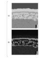
- 3 is an observation photograph of an electrode portion of the thermistor of Example 1 of the present invention in Example.
- 5 is an observation photograph of an electrode portion of the thermistor of Comparative Example 1 in Example.
- the thermistor 10 has, for example, a prism shape, and has a thermistor body 11, a protective film 15 formed on the surface of the thermistor body 11, and a thermistor body. 11 and electrode portions 20 respectively formed at both end portions of the electrode 11.
- the protective film 15 is not formed on both end surfaces of the thermistor element body 11, and the electrode portion 20 is configured to directly contact the thermistor element body 11.
- the thermistor body 11 has a characteristic that its electric resistance changes according to temperature.
- the thermistor body 11 has low resistance to acids and alkalis, and its composition may change due to a reduction reaction or the like, resulting in a large change in characteristics. Therefore, in this embodiment, the protective film 15 for protecting the thermistor element body 11 is formed.
- the protective film 15 is required to have resistance to a plating solution, environment resistance, and insulation. Therefore, in the present embodiment, the protective film 15 may be made of silicon oxide, specifically, SiO 2 . Further, in the present embodiment, the thickness of the protective film 15 is preferably 100 nm or more, and more preferably 300 nm or more in order to prevent the film from becoming a discontinuous film. On the other hand, the upper limit of the thickness of the protective film 15 can be arbitrarily set by selecting an appropriate protective film forming method, but is preferably 3000 nm or less.
- the electrode portion 20 has a two-layer structure including a base electrode layer 21 formed on the end surface of the thermistor element body 11 and a cover electrode layer 22 laminated on the base electrode layer 21.
- the base electrode layer 21 is formed by firing a conductive paste (first conductive paste), and in the present embodiment, may be made of a fired body of Ag. In this case, holes are present inside the base electrode layer 21.
- the cover electrode layer 22 is also formed by firing a conductive paste (second conductive paste) as described later, and in the present embodiment, may be made of a fired body of Ag. In this case, holes also exist inside the cover electrode layer 22.
- the thickness t1 of the base electrode layer 21 is preferably in the range of 2 ⁇ m or more and 20 ⁇ m or less.
- the thickness t1 of the base electrode layer 21 is preferably in the range of 2 ⁇ m or more and 20 ⁇ m or less.
- the lower limit of the thickness t1 of the base electrode layer 21 is preferably 3 ⁇ m or more, more preferably 5 ⁇ m or more.
- the upper limit of the thickness t1 of the base electrode layer 21 is preferably 15 ⁇ m or less, and more preferably 10 ⁇ m or less.
- the thickness t2 of the cover electrode layer 22 is preferably within the range of 3 ⁇ m or more and 20 ⁇ m or less.
- the thickness t2 of the cover electrode layer 22 is set to 3 ⁇ m or more, the amount of glass is secured, and the protective film 15 is appropriately eroded. Further, it is not necessary to increase the glass amount more than necessary to ensure the erosion of the protective film 15, and it is possible to suppress the increase in the resistance value by the percolation of the conductive particles.
- the thickness t2 of the cover electrode layer 22 by setting the thickness t2 of the cover electrode layer 22 to 20 ⁇ m or less, it is possible to suppress material loss and to prevent the element shape from greatly bulging only in the electrode portion.
- the lower limit of the thickness t2 of the cover electrode layer 22 is preferably 4 ⁇ m or more, more preferably 5 ⁇ m or more.
- the upper limit of the thickness t2 of the cover electrode layer 22 is preferably 15 ⁇ m or less, more preferably 10 ⁇ m or less.
- a Ni plating layer 31 is formed on the surface of the electrode portion 20, and a Sn plating layer 32 is formed so as to be stacked on the Ni plating layer 31. Further, in the present embodiment, the penetration depth D of Ni of the Ni plating layer 31 into the electrode portion 20 is set to be less than the thickness t of the electrode portion 20. That is, Ni of the Ni plating layer 31 does not reach the junction interface between the thermistor element body 11 and the electrode portion 20 (base electrode layer 21).
- the thermistor element body 11 having a prismatic shape is manufactured.
- the thermistor element body 11 is manufactured by cutting a plate material made of the thermistor material into strips.
- the protective film 15 is formed on the surface of the thermistor element body 11 described above.
- the thermistor body 11 is immersed in a reaction solution containing silicon alkoxide, water, an organic solvent, and an alkali, and the silicon alkoxide is hydrolyzed and polycondensed to cause a silicon oxide (on the surface of the thermistor body 11).
- the protective film 15 may be formed by depositing (SiO 2 ). Since the chip is cut into a predetermined chip size after the protective film 15 is formed, the protective film 15 is not formed on both end surfaces of the thermistor element body 11 at this stage.
- the base electrode layers 21 are formed on both ends of the thermistor element body 11.
- the protective film 15 is not formed on both end surfaces of the thermistor element body 11, and the base electrode layer 21 is formed so as to directly contact the thermistor element body 11.
- the base electrode layer 21 is formed by applying a conductive paste containing Ag powder and glass powder as the first conductive paste to both ends of the thermistor element body 11 and firing it.
- the electrode layer 21 is composed of a fired body of Ag.
- an oxide layer is formed on the surface of the base electrode layer 21.
- an oxide layer made of silicon oxide is formed by barrel sputtering.
- the thickness of the oxide layer formed is preferably in the range of 0.1 ⁇ m or more and 3 ⁇ m or less.
- the lower limit of the thickness of the oxide layer is preferably 0.2 ⁇ m or more, more preferably 0.3 ⁇ m or more.
- the upper limit of the thickness of the oxide layer is preferably 2 ⁇ m or less, more preferably 1.5 ⁇ m or less.
- the cover electrode layer 22 is formed on the surface of the above oxide layer.
- the cover electrode layer 22 is formed by applying a conductive paste containing Ag powder and glass powder as the second conductive paste onto the surface of the oxide layer and baking the conductive paste. 22 is composed of a fired body of Ag.
- Conduction heat treatment step S06 Next, heat treatment is performed so that the base electrode layer 21 and the cover electrode layer 22 are electrically connected. In this conduction heat treatment step S06, at least a part of the oxide layer disappears, so that the base electrode layer 21 and the cover electrode layer 22 become conductive.
- the heating temperature is equal to or higher than the melting points of both the glass frit in the base electrode layer 21 and the glass frit in the cover electrode layer 22. That is, although the optimum temperature changes depending on the glass frit used, it is preferably higher than the melting point of the glass frit in the cover electrode layer 22 by 50° C. or more, from the viewpoint of sintering Ag powder in the cover electrode layer 22.
- the upper limit of the heating temperature is preferably 900° C. or lower from the viewpoint of the glass floating on the surface of the cover electrode layer 22.
- the melting point of the glass frit in the cover electrode layer 22 is preferably higher than the melting point of the glass frit in the base electrode layer 21.
- the base electrode layer forming step S03 By the base electrode layer forming step S03, the oxide layer forming step S04, the cover electrode layer forming step S05, and the conduction heat treatment step S06, the two-layer structure electrode portion 20 including the base electrode layer 21 and the cover electrode layer 22 is formed. Will be done.
- a metal plating layer is formed on the surface of the electrode portion 20.
- the Ni plating layer 31 is formed on the surface of the electrode portion 20, and then the Sn plating layer 32 is formed so as to be stacked on the Ni plating layer 31.
- the Ni plating layer 31 and the Sn plating layer 32 described above are formed by wet barrel plating.
- the plating solution penetrates into the pores of the electrode portion 20.
- the holes inside the base electrode layer 21 and the holes inside the cover electrode layer 22 do not communicate with each other, the penetration of the plating solution at the bonding interface between the base electrode layer 21 and the cover electrode layer 22 is prevented. Will be suppressed.
- the penetration depth D of Ni of the Ni plating layer 31 into the electrode portion 20 becomes less than the thickness t of the electrode portion 20.
- the thermistor 10 according to the present embodiment is manufactured by the above process.
- the conduction heat treatment step S06 is performed to perform heat treatment so that the base electrode layer 21 and the cover electrode layer 22 are electrically conducted, a space between the base electrode layer 21 and the cover electrode layer 22 is provided. Even if the oxide layer is formed on the base electrode layer 21, the base electrode layer 21 and the cover electrode layer 22 are electrically connected to each other, and the characteristics of the electrode portion 20 can be secured.
- the glass frit and the oxide included in one or both of the base electrode layer 21 and the cover electrode layer 22 are included.
- the base electrode layer 21 and the cover electrode layer 22 are electrically connected by the reaction and erosion of the layers. Therefore, at least one of the base electrode layer 21 and the cover electrode layer 22 needs to include the glass frit, and it is preferable that the glass frit be included in both of them.
- a glass-containing metal paste containing Ag powder and glass powder as the first conductive paste is applied to the end surface of the thermistor element body 11 and baked.
- the adhesion between the thermistor element body 11 and the base electrode layer 21 can be improved.
- the cover electrode layer forming step S05 a metal paste containing glass containing Ag powder and glass powder as the second conductive paste is applied and baked on the surface of the oxide layer.
- the cover electrode layer 22 since the cover electrode layer 22 is formed, the glass and the oxide layer react with each other in the conduction heat treatment step S06, whereby at least a part of the oxide layer can be efficiently eliminated, and the base electrode layer 21 and the cover electrode layer 22 can be sufficiently conducted.
- the oxide formed between the base electrode layer 21 and the cover electrode layer 22 is composed of silicon oxide, it becomes an oxide layer having excellent environment resistance,
- the cover electrode layer 22 can be reliably formed on the surface of the oxide layer, and the electrode portion 20 having a two-layer structure of the base electrode layer 21 and the cover electrode layer 22 can be stably formed. it can.
- the electrode portion 20 has a two-layer structure including the base electrode layer 21 and the cover electrode layer 22, and the Ni forming the Ni plating layer 31 enters the electrode portion 20. Since the depth D is less than the thickness t of the electrode portion 20, contact between the plating solution and the thermistor element body 11 in the plating step S07 is suppressed. Further, Ni is also prevented from being deposited at the interface between the thermistor element body 11 and the electrode portion 20 (base electrode layer 21). Therefore, the thermistor 10 having various stable characteristics can be provided.
- the present invention is not limited to this, and can be appropriately modified without departing from the technical idea of the invention.
- the description has been made assuming that the thermistor body is immersed in the reaction solution to form the protective film, but the present invention is not limited to this, and the protective film may be formed by other means.
- a glass paste may be applied and baked to form a protective film.
- the base electrode layer is formed on the end surface of the thermistor element body, but the invention is not limited to this, and the end surface of the thermistor element body is not limited to this.
- an oxide film may be formed on the entire surface of the thermistor element body on which the base electrode layer is formed, and the oxide layer and the protective film may be formed at the same time. That is, the protective film forming step and the oxide layer forming step may be performed at the same time.
- the base electrode layer and the cover electrode layer are described as being formed of a fired body of Ag in the present embodiment, the present invention is not limited to this, and for example, an Ag alloy such as an Ag—Pd alloy or Au. , Pt, Rh, Ir, Ru oxide, and a fired body composed of a mixture thereof may be used.
- the base electrode layer and the cover electrode layer may be made of different materials.
- the oxide layer is described as being composed of silicon oxide, but the oxide layer is not limited to this, and may be composed of other oxides such as alumina and titania. ..
- Example 2 A silicon oxide film (protective film and oxide layer) was formed in the same manner as in Example 1 of the present invention except that the film thickness was 0.1 ⁇ m and the cover electrode layer was formed of Au paste.
- the base electrode layer and the cover electrode layer are formed by using a conductive paste containing a metal powder of Ag-5 mass% Pd, and the thickness of the silicon oxide film (protective film and oxide layer) is set to 0.5 ⁇ m. Except for the above, it was prepared in the same manner as in Example 1 of the present invention.
- RuO 2 powder of high purity chemical was used as a raw material on both sides of a thermistor wafer having a size of 38 ⁇ 55 mm and a thickness of 0.36 mm, and a RuO 2 concentration of 10 wt. % Ethanol dispersion was spin-coated to form a RuO 2 intermediate layer. Further, a glass frit-containing Ag paste was printed on both surfaces of the wafer by screen printing and baked under the conditions of 800° C. and 10 minutes in the atmosphere to form a base electrode layer. The thermistor wafer having the underlying electrode layer thus formed was attached to a dicing tape and cut into chips of 0.18 mm square by dicing with a diamond blade.
- the thermistor chip prepared as described above is placed in a water-ethanol mixed solvent, and ethyl orthosilicate and an aqueous NaOH solution are added with stirring to hydrolyze or polycondense the ethyl orthosilicate to thereby obtain 0.5 ⁇ m silicon oxide.
- a material film (protective film and oxide layer) was formed. After that, the same procedure as in Inventive Example 1 was performed.
- Example 6 A base electrode layer was formed by Au paste, and the same process as in Example 5 of the present invention was performed except that the silicon oxide film (protective film and oxide layer) had a thickness of 1.0 ⁇ m.
- the underlayer electrode layer was formed of Pt paste, and the film was prepared in the same manner as Example 5 of the present invention, except that the silicon oxide film (protective film and oxide layer) had a thickness of 1.2 ⁇ m.
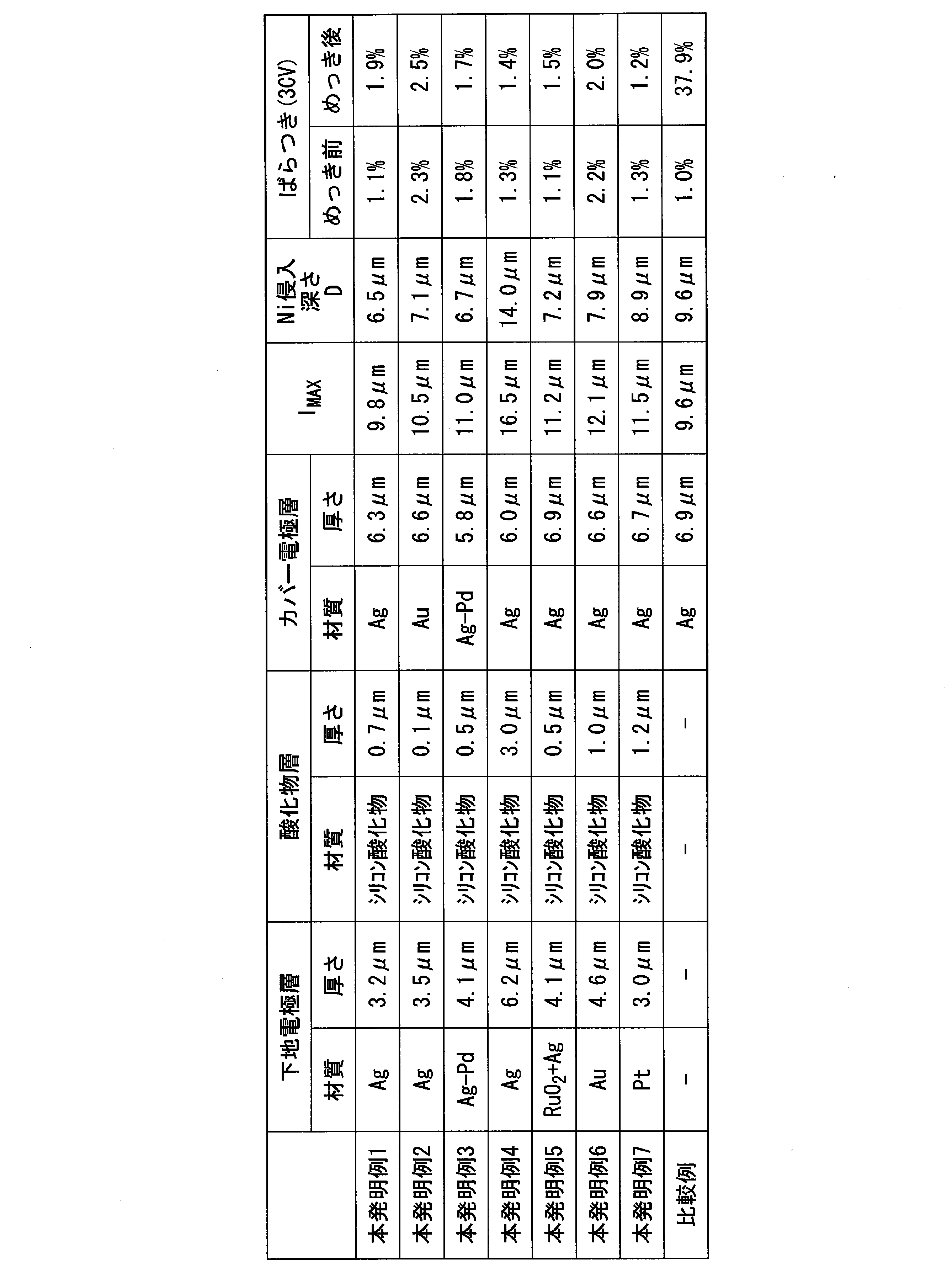
- the distance from the point where the component of the plating layer was detected to the thermistor element was defined as d, and its minimum value was defined as d MIN .
- the value of l MAX ⁇ d MIN was defined as the penetration depth D of the plating layer.
- the thickness of the electrode part was set to 1 MAX .
- example 1-7 in which the electrode portion has a two-layer structure and the penetration depth D of Ni is less than the thickness of the electrode portion as shown in FIG. There was no significant change, and the characteristics of the thermistor body were sufficiently stable.
- the thermistor element has stable characteristics. It has been confirmed that it is possible to provide a thermistor manufacturing method for manufacturing a thermistor, and a thermistor manufactured by this thermistor manufacturing method and having stable characteristics.
Landscapes
- Engineering & Computer Science (AREA)
- Chemical & Material Sciences (AREA)
- Microelectronics & Electronic Packaging (AREA)
- Chemical Kinetics & Catalysis (AREA)
- Materials Engineering (AREA)
- Metallurgy (AREA)
- Organic Chemistry (AREA)
- Electrochemistry (AREA)
- Physics & Mathematics (AREA)
- Electromagnetism (AREA)
- Mechanical Engineering (AREA)
- Manufacturing & Machinery (AREA)
- General Chemical & Material Sciences (AREA)
- Life Sciences & Earth Sciences (AREA)
- Pest Control & Pesticides (AREA)
- Thermal Sciences (AREA)
- Ceramic Engineering (AREA)
- Thermistors And Varistors (AREA)
- Apparatuses And Processes For Manufacturing Resistors (AREA)
- Details Of Resistors (AREA)
Abstract
サーミスタ素体の端面に導電性ペーストを塗布して焼成し、下地電極層を形成する下地電極層形成工程(S03)と、前記下地電極層の表面に酸化物層を形成する酸化物層形成工程(S04)と、前記酸化物層の表面に導電性ペーストを塗布して焼成し、カバー電極層を形成するカバー電極層形成工程(S05)と、前記下地電極層と前記カバー電極層とが電気的に導通するように熱処理を行う導通熱処理工程(S06)と、を有し、前記下地電極層と前記カバー電極層とを有する前記電極部を形成するとともに、導通熱処理工程(S06)後に、前記カバー電極層の表面に金属めっき層を形成するめっき工程(S07)を備えている。
Description
この発明は、サーミスタ素体と、前記サーミスタ素体の端面に形成された電極部と、を備えたサーミスタを製造するサーミスタの製造方法、及び、サーミスタに関するものである。
本願は、2019年2月15日に日本に出願された、特願2019-025313号に基づき優先権主張し、その内容をここに援用する。
本願は、2019年2月15日に日本に出願された、特願2019-025313号に基づき優先権主張し、その内容をここに援用する。
上述のサーミスタにおいては、温度に応じて電気抵抗が変化する特性を有しており、各種電子機器の温度補償や温度センサ等に適用されている。特に、最近では、回路基板に実装されるチップ型サーミスタが広く使用されている。
上述のサーミスタは、サーミスタ素体と、このサーミスタ素体の両端に一対の電極部を形成した構造としている。
上述のサーミスタは、サーミスタ素体と、このサーミスタ素体の両端に一対の電極部を形成した構造としている。
サーミスタ素体は、酸やアルカリに弱く、かつ、還元しやすい性質を有している。そして、組成が変化すると特性が変動してしまうおそれがあった。このため、例えば特許文献1に示すように、サーミスタ素体の表面に保護膜を成膜する技術が提案されている。なお、保護膜には、その後の工程や使用時におけるサーミスタ素体の劣化を抑制するために、めっき液への耐性、耐環境性、絶縁性、等が要求される。
ここで、特許文献1においては、サーミスタ素体の表面にガラスペーストを塗布して焼成することにより、厚膜のガラスからなる保護膜を成膜している。
また、サーミスタ素体の両端に電極部を形成することになるため、電極部が形成されるサーミスタの端面には保護膜が形成されてない。ここで、電極部は、サーミスタ素体の両端に、例えばAg等の導電性材料を含む導電性ペーストを塗布して焼成することによって形成される。また、焼成体からなる電極部の表面には、Niめっき層やSnめっき層が形成される。
また、サーミスタ素体の両端に電極部を形成することになるため、電極部が形成されるサーミスタの端面には保護膜が形成されてない。ここで、電極部は、サーミスタ素体の両端に、例えばAg等の導電性材料を含む導電性ペーストを塗布して焼成することによって形成される。また、焼成体からなる電極部の表面には、Niめっき層やSnめっき層が形成される。
ところで、特許文献1に示すように、サーミスタ素体の端面に導電性ペーストの焼成体からなる電極部を形成した場合には、導電性ペーストの塗布ムラや導電性ペーストへの異物の混入により、電極部に空孔が生じてポーラスな構造となることがあった。このような電極部に対してめっき層を形成した場合には、電極部の内部にめっき液が侵入し、サーミスタ素体とめっき液とが接触して、サーミスタ素体が劣化するおそれがあった。また、サーミスタ素体と電極部の界面にめっき金属が析出し、めっきの前後で抵抗値が大きく変化してしまうおそれがあった。
この発明は、前述した事情に鑑みてなされたものであって、電極部の表面にめっき層を形成した場合であっても、電極部内部へのめっき液の侵入を抑制でき、サーミスタ素体の特性が安定したサーミスタを製造することが可能なサーミスタの製造方法、及び、このサーミスタの製造方法により製造され、特性の安定したサーミスタを提供することを目的とする。
上記課題を解決するために、本発明のサーミスタの製造方法は、サーミスタ素体と、前記サーミスタ素体の端面に形成された電極部と、を備えたサーミスタを製造するサーミスタの製造方法であって、前記サーミスタ素体の端面に導電性ペースト(以下、「第1の導電性ペースト」という場合がある。)を塗布して焼成し、下地電極層を形成する下地電極層形成工程と、前記下地電極層の表面に酸化物層を形成する酸化物層形成工程と、前記酸化物層の表面に導電性ペースト(以下、「第2の導電性ペースト」という場合がある。)を塗布して焼成し、カバー電極層を形成するカバー電極層形成工程と、前記下地電極層と前記カバー電極層とが電気的に導通するように熱処理を行う導通熱処理工程と、を有し、前記下地電極層と前記カバー電極層とを有する前記電極部を形成するとともに、前記導通熱処理工程後に、前記カバー電極層の表面に金属めっき層を形成するめっき工程を備えていることを特徴としている。
本発明のサーミスタの製造方法によれば、上述のように、下地電極層形成工程と、酸化物層形成工程と、カバー電極層形成工程と、導通熱処理工程と、によって電極部を形成しているので、電極部が下地電極層とカバー電極層の2層構造となり、下地電極層内の空孔とカバー電極層の空孔とが連通することなく、めっき工程において、めっき液の侵入がカバー電極層と下地電極層との界面において阻止されることになり、サーミスタ素体とめっき液との接触を抑制することが可能となる。また、サーミスタ素体と電極部の界面にめっき金属が析出することを抑制できる。
また、前記下地電極層と前記カバー電極層とが電気的に導通するように熱処理を行う導通熱処理工程を備えているので、下地電極層とカバー電極層との間に酸化物層を形成しても、下地電極層とカバー電極層とを電気的に導通させることができ、電極部としての特性を確保することが可能となる。なお、酸化物層形成工程で形成された酸化物層は、下地電極層とカバー電極層との導通が十分であれば、下地電極層とカバー電極層の界面に残存していてもよいし、導通熱処理工程において完全に消失してもよい。
ここで、本発明のサーミスタの製造方法においては、前記下地電極層形成工程は、金属粉とガラス粉とを含有するガラス入り金属ペーストを塗布して焼成することにより、前記下地電極層を形成する構成としてもよい。すなわち、本発明のサーミスタの製造方法においては、前記第1の導電性ペーストが、金属粉とガラス粉とを含有するガラス入り金属ペーストである構成としてもよい。
この場合、前記第1のペーストとしてガラス入り金属ペーストを焼成することによって下地電極層を形成しているので、サーミスタ素体との下地電極層との密着性を向上させることができる。
この場合、前記第1のペーストとしてガラス入り金属ペーストを焼成することによって下地電極層を形成しているので、サーミスタ素体との下地電極層との密着性を向上させることができる。
また、本発明のサーミスタの製造方法においては、前記カバー電極層形成工程は、金属粉とガラス粉とを含有するガラス入り金属ペーストを塗布して焼成することにより、前記カバー電極層を形成する構成としてもよい。すなわち、本発明のサーミスタの製造方法においては、前記第2の導電性ペーストが、金属粉とガラス粉とを含有するガラス入り金属ペーストである構成としてもよい。
この場合、前記第2の導電性ペーストとしてガラス入り金属ペーストを焼成することによってカバー電極層を形成しているので、導通熱処理工程において、ガラスと酸化物層とが反応することで、酸化物層の少なくとも一部を効率良く消滅させることができ、下地電極層とカバー電極層とを十分に導通させることが可能となる。
この場合、前記第2の導電性ペーストとしてガラス入り金属ペーストを焼成することによってカバー電極層を形成しているので、導通熱処理工程において、ガラスと酸化物層とが反応することで、酸化物層の少なくとも一部を効率良く消滅させることができ、下地電極層とカバー電極層とを十分に導通させることが可能となる。
さらに、本発明のサーミスタの製造方法においては、前記酸化物層は、シリコン酸化物で構成されていることが好ましい。
この場合、酸化物層がシリコン酸化物で構成されているので、耐環境性に優れており、この酸化物層の表面に確実にカバー電極層を形成することができ、下地電極層とカバー電極層の2層構造電極部を安定して形成することができる。
この場合、酸化物層がシリコン酸化物で構成されているので、耐環境性に優れており、この酸化物層の表面に確実にカバー電極層を形成することができ、下地電極層とカバー電極層の2層構造電極部を安定して形成することができる。
本発明のサーミスタは、サーミスタ素体と、前記サーミスタ素体の端面に形成された電極部と、を備えたサーミスタであって、前記電極部は、前記サーミスタ素体の端面に形成された下地電極層と、前記下地電極層に積層するカバー電極層と、を備えており、この電極部の表面に金属めっき層が形成されており、前記金属めっき層を構成するめっき金属の前記電極部への侵入深さが、前記電極部の厚さ未満とされていることを特徴としている。
この構成のサーミスタによれば、電極部が下地電極層とカバー電極層との2層構造とされており、金属めっき層を構成するめっき金属の前記電極部への侵入深さが、前記電極部の厚さ未満とされているので、めっき時におけるめっき液とサーミスタ素体との接触が抑制されている。また、サーミスタ素体と電極部の界面にめっき金属が析出することも抑制されている。よって、各種特性が安定したサーミスタを提供することができる。
本発明によれば、電極部の表面にめっき層を形成した場合であっても、電極部内部へのめっき液の侵入を抑制でき、サーミスタ素体の特性が安定したサーミスタを製造することが可能なサーミスタの製造方法、及び、このサーミスタの製造方法により製造され、特性の安定したサーミスタを提供することができる。
以下に、本発明の実施形態について添付した図面を参照して説明する。なお、以下に示す各実施形態は、発明の趣旨をより良く理解させるために具体的に説明するものであり、特に指定のない限り、本発明を限定するものではない。また、以下の説明で用いる図面は、本発明の特徴をわかりやすくするために、便宜上、要部となる部分を拡大して示している場合があり、各構成要素の寸法比率などが実際と同じであるとは限らない。
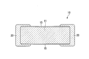
本実施形態に係るサーミスタ10は、図1に示すように、例えば、角柱状をなしており、サーミスタ素体11と、このサーミスタ素体11の表面に形成された保護膜15と、サーミスタ素体11の両端部にそれぞれ形成された電極部20と、を備えている。
ここで、図1に示すように、保護膜15は、サーミスタ素体11の両端面には形成されておらず、電極部20は、サーミスタ素体11に直接接触するように構成されている。
ここで、図1に示すように、保護膜15は、サーミスタ素体11の両端面には形成されておらず、電極部20は、サーミスタ素体11に直接接触するように構成されている。
サーミスタ素体11は、温度に応じて電気抵抗が変化する特性を有している。このサーミスタ素体11は、酸やアルカリに対する耐性が低く、還元反応等によって組成が変化し、特性が大きく変動してしまうおそれがある。よって、本実施形態では、サーミスタ素体11を保護するための保護膜15が形成されている。
ここで、保護膜15には、めっき液に対する耐性、耐環境性、絶縁性が求められる。そこで、本実施形態では、保護膜15は、シリコン酸化物、具体的には、SiO2で構成されていてもよい。
また、本実施形態においては、保護膜15の厚さは、不連続膜となることを抑制するために100nm以上とすることが好ましく、300nm以上とすることがさらに好ましい。一方、保護膜15の厚さの上限は、適当な保護膜の形成方法を選定することで、任意に設定することができるが、3000nm以下とすることが好ましい。
また、本実施形態においては、保護膜15の厚さは、不連続膜となることを抑制するために100nm以上とすることが好ましく、300nm以上とすることがさらに好ましい。一方、保護膜15の厚さの上限は、適当な保護膜の形成方法を選定することで、任意に設定することができるが、3000nm以下とすることが好ましい。
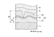
電極部20は、図2に示すように、サーミスタ素体11の端面に形成された下地電極層21と、この下地電極層21に積層配置されたカバー電極層22と、を備えた2層構造とされている。
下地電極層21は、後述するように、導電性ペースト(第1の導電性ペースト)を焼成して形成されており、本実施形態では、Agの焼成体で構成されていてもよい。この場合、下地電極層21の内部には、空孔が存在することになる。
また、カバー電極層22も、後述するように、導電性ペースト(第2の導電性ペースト)を焼成して形成されており、本実施形態では、Agの焼成体で構成されていてもよい。この場合、カバー電極層22の内部にも、空孔が存在することになる。
下地電極層21は、後述するように、導電性ペースト(第1の導電性ペースト)を焼成して形成されており、本実施形態では、Agの焼成体で構成されていてもよい。この場合、下地電極層21の内部には、空孔が存在することになる。
また、カバー電極層22も、後述するように、導電性ペースト(第2の導電性ペースト)を焼成して形成されており、本実施形態では、Agの焼成体で構成されていてもよい。この場合、カバー電極層22の内部にも、空孔が存在することになる。
ここで、下地電極層21の厚さt1は、2μm以上20μm以下の範囲内とすることが好ましい。
下地電極層21の厚さt1を2μm以上とすることでガラス量が確保され、適格に保護膜15の浸食が起こる。また、保護膜15の浸食を担保するためにガラス量を必要以上に増加する必要がなく、導電性粒子のパーコレーションにより、抵抗値の上昇を抑制することができる。一方、下地電極層21の厚さt1を20μm以下とすることで、材料のロスを抑制することができる。
なお、下地電極層21の厚さt1の下限は、3μm以上とすることが好ましく、5μm以上とすることがさらに好ましい。一方、下地電極層21厚さt1の上限は、15μm以下とすることが好ましく、10μm以下とすることがさらに好ましい。
下地電極層21の厚さt1を2μm以上とすることでガラス量が確保され、適格に保護膜15の浸食が起こる。また、保護膜15の浸食を担保するためにガラス量を必要以上に増加する必要がなく、導電性粒子のパーコレーションにより、抵抗値の上昇を抑制することができる。一方、下地電極層21の厚さt1を20μm以下とすることで、材料のロスを抑制することができる。
なお、下地電極層21の厚さt1の下限は、3μm以上とすることが好ましく、5μm以上とすることがさらに好ましい。一方、下地電極層21厚さt1の上限は、15μm以下とすることが好ましく、10μm以下とすることがさらに好ましい。
また、カバー電極層22の厚さt2は、3μm以上20μm以下の範囲内とすることが好ましい。
カバー電極層22の厚さt2を3μm以上とすることでガラス量が確保され、適格に保護膜15の浸食が起こる。また、保護膜15の浸食を担保するためにガラス量を必要以上に増加する必要がなく、導電性粒子のパーコレーションにより、抵抗値の上昇を抑制することができる。一方、カバー電極層22の厚さt2を20μm以下とすることで、材料のロスを抑制することができるとともに、素子形状が電極部分のみ大きく膨らむことを抑制できる。
なお、カバー電極層22の厚さt2の下限は、4μm以上とすることが好ましく、5μm以上とすることがさらに好ましい。一方、カバー電極層22の厚さt2の上限は、15μm以下とすることが好ましく、10μm以下とすることがさらに好ましい。
カバー電極層22の厚さt2を3μm以上とすることでガラス量が確保され、適格に保護膜15の浸食が起こる。また、保護膜15の浸食を担保するためにガラス量を必要以上に増加する必要がなく、導電性粒子のパーコレーションにより、抵抗値の上昇を抑制することができる。一方、カバー電極層22の厚さt2を20μm以下とすることで、材料のロスを抑制することができるとともに、素子形状が電極部分のみ大きく膨らむことを抑制できる。
なお、カバー電極層22の厚さt2の下限は、4μm以上とすることが好ましく、5μm以上とすることがさらに好ましい。一方、カバー電極層22の厚さt2の上限は、15μm以下とすることが好ましく、10μm以下とすることがさらに好ましい。
また、電極部20の表面には、Niめっき層31が形成され、このNiめっき層31に積層するようにSnめっき層32が形成されている。
そして、本実施形態においては、Niめっき層31のNiの電極部20への侵入深さDが、電極部20の厚さt未満とされている。すなわち、Niめっき層31のNiが、サーミスタ素体11と電極部20(下地電極層21)との接合界面にまで達していないのである。
そして、本実施形態においては、Niめっき層31のNiの電極部20への侵入深さDが、電極部20の厚さt未満とされている。すなわち、Niめっき層31のNiが、サーミスタ素体11と電極部20(下地電極層21)との接合界面にまで達していないのである。
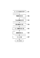
次に、上述した本実施形態であるサーミスタ10の製造方法について、図3のフロー図を用いて説明する。
(サーミスタ素体形成工程S01)
まず、角柱状をなすサーミスタ素体11を製造する。本実施形態においては、サーミスタ材料からなる板材を短冊状に切断することにより、上述のサーミスタ素体11を製造している。
まず、角柱状をなすサーミスタ素体11を製造する。本実施形態においては、サーミスタ材料からなる板材を短冊状に切断することにより、上述のサーミスタ素体11を製造している。
(保護膜形成工程S02)
次に、上述のサーミスタ素体11の表面に保護膜15を成膜する。本実施形態では、サーミスタ素体11を、シリコンアルコキシドと水と有機溶媒とアルカリを含む反応液に浸漬し、シリコンアルコキシドの加水分解及び重縮合反応により、サーミスタ素体11の表面にシリコン酸化物(SiO2)を析出させることにより、保護膜15を成膜してもよい。
なお、保護膜15の形成後に所定のチップサイズに切断するため、この段階では、サーミスタ素体11の両端面には、保護膜15は形成されない。
次に、上述のサーミスタ素体11の表面に保護膜15を成膜する。本実施形態では、サーミスタ素体11を、シリコンアルコキシドと水と有機溶媒とアルカリを含む反応液に浸漬し、シリコンアルコキシドの加水分解及び重縮合反応により、サーミスタ素体11の表面にシリコン酸化物(SiO2)を析出させることにより、保護膜15を成膜してもよい。
なお、保護膜15の形成後に所定のチップサイズに切断するため、この段階では、サーミスタ素体11の両端面には、保護膜15は形成されない。
(下地電極層形成工程S03)
次に、サーミスタ素体11の両端部に下地電極層21を形成する。なお、サーミスタ素体11の両端面には保護膜15が形成されておらず、サーミスタ素体11に直接接触するように、下地電極層21を形成することになる。
本実施形態では、第1の導電性ペーストとしてAg粉とガラス粉を含む導電性ペーストをサーミスタ素体11の両端部に塗布して焼成することにより、下地電極層21を形成しており、下地電極層21は、Agの焼成体で構成されることになる。
次に、サーミスタ素体11の両端部に下地電極層21を形成する。なお、サーミスタ素体11の両端面には保護膜15が形成されておらず、サーミスタ素体11に直接接触するように、下地電極層21を形成することになる。
本実施形態では、第1の導電性ペーストとしてAg粉とガラス粉を含む導電性ペーストをサーミスタ素体11の両端部に塗布して焼成することにより、下地電極層21を形成しており、下地電極層21は、Agの焼成体で構成されることになる。
(酸化物層形成工程S04)
次に、下地電極層21の表面に酸化物層を形成する。本実施形態では、バレルスパッタによって、シリコン酸化物からなる酸化物層を形成する。
ここで、形成される酸化物層の厚さは、0.1μm以上3μm以下の範囲内とすることが好ましい。なお、酸化物層の厚さの下限は、0.2μm以上であることが好ましく、0.3μm以上であることがさらに好ましい。一方、酸化物層の厚さの上限は、2μm以下であることが好ましく、1.5μm以下であることがさらに好ましい。
次に、下地電極層21の表面に酸化物層を形成する。本実施形態では、バレルスパッタによって、シリコン酸化物からなる酸化物層を形成する。
ここで、形成される酸化物層の厚さは、0.1μm以上3μm以下の範囲内とすることが好ましい。なお、酸化物層の厚さの下限は、0.2μm以上であることが好ましく、0.3μm以上であることがさらに好ましい。一方、酸化物層の厚さの上限は、2μm以下であることが好ましく、1.5μm以下であることがさらに好ましい。
(カバー電極層形成工程S05)
次に、上述の酸化物層の表面にカバー電極層22を形成する。
本実施形態では、第2の導電性ペーストとしてAg粉とガラス粉を含む導電性ペーストを酸化物層の表面に塗布して焼成することにより、カバー電極層22を形成しており、カバー電極層22は、Agの焼成体で構成されることになる。
次に、上述の酸化物層の表面にカバー電極層22を形成する。
本実施形態では、第2の導電性ペーストとしてAg粉とガラス粉を含む導電性ペーストを酸化物層の表面に塗布して焼成することにより、カバー電極層22を形成しており、カバー電極層22は、Agの焼成体で構成されることになる。
(導通熱処理工程S06)
次に、下地電極層21とカバー電極層22とが電気的に導通するように熱処理を実施する。この導通熱処理工程S06においては、酸化物層の少なくとも一部が消失することにより、下地電極層21とカバー電極層22とが導通することになる。
ここで、導通熱処理工程S06においては、加熱温度が下地電極層21中のガラスフリットとカバー電極層22中のガラスフリット両方の融点以上であることが必要である。つまり、使用するガラスフリットによって最適温度は変化することになるが、カバー電極層22中のガラスフリットの融点より50℃以上高いことが好ましく、カバー電極層22中のAg粉の焼結の観点から700℃以上であることがさらに好ましい。加熱温度の上限はカバー電極層22の表面へのガラスの浮きの観点から900℃以下であることが好ましい。また、下地電極層21中のガラスフリットの融点よりも、カバー電極層22中のガラスフリットの融点が高いことが好ましい。
次に、下地電極層21とカバー電極層22とが電気的に導通するように熱処理を実施する。この導通熱処理工程S06においては、酸化物層の少なくとも一部が消失することにより、下地電極層21とカバー電極層22とが導通することになる。
ここで、導通熱処理工程S06においては、加熱温度が下地電極層21中のガラスフリットとカバー電極層22中のガラスフリット両方の融点以上であることが必要である。つまり、使用するガラスフリットによって最適温度は変化することになるが、カバー電極層22中のガラスフリットの融点より50℃以上高いことが好ましく、カバー電極層22中のAg粉の焼結の観点から700℃以上であることがさらに好ましい。加熱温度の上限はカバー電極層22の表面へのガラスの浮きの観点から900℃以下であることが好ましい。また、下地電極層21中のガラスフリットの融点よりも、カバー電極層22中のガラスフリットの融点が高いことが好ましい。
これら下地電極層形成工程S03、酸化物層形成工程S04、カバー電極層形成工程S05、導通熱処理工程S06により、下地電極層21とカバー電極層22とを備えた2層構造の電極部20が形成されることになる。
(めっき工程S07)
次に、電極部20の表面に金属めっき層を形成する。本実施形態では、電極部20の表面にNiめっき層31を形成し、その後、Niめっき層31に積層するようにSnめっき層32を形成する。なお、本実施形態では、湿式のバレルめっきによって、上述のNiめっき層31及びSnめっき層32を形成している。
次に、電極部20の表面に金属めっき層を形成する。本実施形態では、電極部20の表面にNiめっき層31を形成し、その後、Niめっき層31に積層するようにSnめっき層32を形成する。なお、本実施形態では、湿式のバレルめっきによって、上述のNiめっき層31及びSnめっき層32を形成している。
ここで、Niめっき層31を形成する際に、電極部20の空孔内部にめっき液が侵入することになる。本実施形態では、下地電極層21内部の空孔とカバー電極層22の内部の空孔とが連通していないため、下地電極層21とカバー電極層22の接合界面において、めっき液の侵入が抑制されることになる。
これにより、Niめっき層31のNiの電極部20への侵入深さDが、電極部20の厚さt未満となる。
これにより、Niめっき層31のNiの電極部20への侵入深さDが、電極部20の厚さt未満となる。
以上の工程により、本実施形態であるサーミスタ10が製造されることになる。
以上のような構成とされた本実施形態であるサーミスタ10の製造方法によれば、下地電極層形成工程S03と、酸化物層形成工程S04と、カバー電極層形成工程S05と、導通熱処理工程S06と、によって電極部20を形成しているので、電極部20が下地電極層21とカバー電極層22の2層構造となり、下地電極層21内の空孔とカバー電極層22の空孔とが連通することなく、その後のめっき工程S07において、めっき液の侵入がカバー電極層22と下地電極層21との界面において阻止されることになり、サーミスタ素体11とめっき液との接触を抑制することが可能となる。また、サーミスタ素体11と電極部20の界面にNiが析出することを抑制できる。
また、本実施形態においては、下地電極層21とカバー電極層22とが電気的に導通するように熱処理を行う導通熱処理工程S06を備えているので、下地電極層21とカバー電極層22の間に酸化物層を形成した場合であっても、下地電極層21とカバー電極層22とが電気的に導通することになり、電極部20としての特性を確保することが可能となる。
なお、下地電極層21とカバー電極層22とが電気的に導通するように熱処理を行う導通熱処理工程S06では、下地電極層21及びカバー電極層22の一方または両方に含まれるガラスフリットと酸化物層が反応、浸食されることによって下地電極層21とカバー電極層22が導通することになる。このため、少なくとも下地電極層21及びカバー電極層22のいずれか一方にガラスフリットが含まれている必要があり、両方に含まれることが好ましい。
なお、下地電極層21とカバー電極層22とが電気的に導通するように熱処理を行う導通熱処理工程S06では、下地電極層21及びカバー電極層22の一方または両方に含まれるガラスフリットと酸化物層が反応、浸食されることによって下地電極層21とカバー電極層22が導通することになる。このため、少なくとも下地電極層21及びカバー電極層22のいずれか一方にガラスフリットが含まれている必要があり、両方に含まれることが好ましい。
さらに、本実施形態においては、下地電極層形成工程S03において、サーミスタ素体11の端面に、第1の導電性ペーストとしてAg粉とガラス粉とを含有するガラス入り金属ペーストを塗布して焼成することにより、下地電極層21を形成しているので、サーミスタ素体11との下地電極層21との密着性を向上させることができる。
また、本実施形態においては、カバー電極層形成工程S05において、酸化物層の表面に、第2の導電性ペーストとしてAg粉とガラス粉とを含有するガラス入り金属ペーストを塗布して焼成することにより、カバー電極層22を形成しているので、導通熱処理工程S06において、ガラスと酸化物層とが反応することで、酸化物層の少なくとも一部を効率良く消滅させることができ、下地電極層21とカバー電極層22とを十分に導通させることが可能となる。
さらに、本実施形態においては、下地電極層21とカバー電極層22との間に形成される酸化物が、シリコン酸化物で構成されているので、耐環境性に優れた酸化物層となり、カバー電極層形成工程S05において酸化物層の表面に確実にカバー電極層22を形成することができ、下地電極層21とカバー電極層22の2層構造の電極部20を安定して形成することができる。
さらに、本実施形態であるサーミスタ10においては、電極部20が下地電極層21とカバー電極層22との2層構造とされており、Niめっき層31を構成するNiの電極部20への侵入深さDが、電極部20の厚さt未満とされているので、めっき工程S07におけるめっき液とサーミスタ素体11との接触が抑制される。また、サーミスタ素体11と電極部20(下地電極層21)の界面にNiが析出することも抑制されている。よって、各種特性が安定したサーミスタ10を提供することができる。
以上、本発明の一実施形態について説明したが、本発明はこれに限定されることはなく、その発明の技術的思想を逸脱しない範囲で適宜変更可能である。
例えば、本実施形態では、サーミスタ素体を反応液に浸漬して保護膜を成膜するものとして説明したが、これに限定されることはなく、その他の手段によって保護膜を成膜してもよい。例えばガラスペーストを塗布して焼成して保護膜を成膜してもよい。
例えば、本実施形態では、サーミスタ素体を反応液に浸漬して保護膜を成膜するものとして説明したが、これに限定されることはなく、その他の手段によって保護膜を成膜してもよい。例えばガラスペーストを塗布して焼成して保護膜を成膜してもよい。
また、本実施形態では、サーミスタ素体に保護膜を形成した後、サーミスタ素体の端面に下地電極層を形成するものとして説明したが、これに限定されることはなく、サーミスタ素体の端面に下地電極層を形成した後に、下地電極層を形成したサーミスタ素体の全面に酸化物膜を成膜し、酸化物層と保護膜とを同時に形成してもよい。すなわち、保護膜形成工程と酸化物層形成工程を同時に実施してもよい。
さらに、本実施形態では、下地電極層及びカバー電極層をAgの焼成体で構成したものとして説明したが、これに限定されることはなく、例えば、Ag-Pd合金等のAg合金や、Au,Pt,Rh,Ir,Ru酸化物、及び、これらの混合物からなる焼成体で構成したものであってもよい。また、下地電極層とカバー電極層とを、異なる材質で構成してもよい。
また、本実施形態では、酸化物層をシリコン酸化物で構成したものとして説明したが、これに限定されることはなく、アルミナ、チタニア等の他の酸化物で構成したものであってもよい。
本発明の有効性を確認するために行った確認実験について説明する。
(本発明例1)
38×55mm、厚さ0.36mmのサーミスタウェハ両面に、スクリーン印刷によってガラスフリット入りのAgペーストを前記ウェハ両面に印刷、焼き付けることで、下地電極層を形成した。このように下地電極層を形成したサーミスタウェハをダイシングテープに貼り付け、ダイヤモンドブレードを用いたダイシングによって0.18mm角に切断、チップ化した。
上記のように作製したサーミスタチップにバレルスパッタによって0.7μmのシリコン酸化物膜(保護膜及び酸化物層)を形成した。
酸化物層の表面にAgペーストをディッピング、焼き付けを行うことでカバー電極層を形成した。
次に、雰囲気:大気、加熱温度:700℃、加熱温度での保持時間:10分の条件で導通熱処理を実施した。
その後、湿式のバレルめっきによってカバー電極層上にNiめっき層を形成し、さらに、Niめっき層上にSnめっき層を形成した。
38×55mm、厚さ0.36mmのサーミスタウェハ両面に、スクリーン印刷によってガラスフリット入りのAgペーストを前記ウェハ両面に印刷、焼き付けることで、下地電極層を形成した。このように下地電極層を形成したサーミスタウェハをダイシングテープに貼り付け、ダイヤモンドブレードを用いたダイシングによって0.18mm角に切断、チップ化した。
上記のように作製したサーミスタチップにバレルスパッタによって0.7μmのシリコン酸化物膜(保護膜及び酸化物層)を形成した。
酸化物層の表面にAgペーストをディッピング、焼き付けを行うことでカバー電極層を形成した。
次に、雰囲気:大気、加熱温度:700℃、加熱温度での保持時間:10分の条件で導通熱処理を実施した。
その後、湿式のバレルめっきによってカバー電極層上にNiめっき層を形成し、さらに、Niめっき層上にSnめっき層を形成した。
(本発明例2)
シリコン酸物膜(保護膜及び酸化物層)の膜厚を0.1μmとし、カバー電極層をAuペーストによって形成した以外は、本発明例1と同様に作製した。
シリコン酸物膜(保護膜及び酸化物層)の膜厚を0.1μmとし、カバー電極層をAuペーストによって形成した以外は、本発明例1と同様に作製した。
(本発明例3)
下地電極層およびカバー電極層を、Ag-5mass%Pdからなる金属粉を含有する導電性ペーストを用いて形成し、シリコン酸物膜(保護膜及び酸化物層)の膜厚を0.5μmとした以外は、本発明例1と同様に作製した。
下地電極層およびカバー電極層を、Ag-5mass%Pdからなる金属粉を含有する導電性ペーストを用いて形成し、シリコン酸物膜(保護膜及び酸化物層)の膜厚を0.5μmとした以外は、本発明例1と同様に作製した。
(本発明例4)
38×55mm、厚さ0.15mmのサーミスタウェハ両面に、スクリーン印刷によってガラスペーストを印刷、焼き付け後、ダイヤモンドブレードを用いたダイシングによって0.15mm幅の短冊状に切断した。さらに、切断面両面にスクリーン印刷によってガラスペーストを印刷、焼き付け後、ダイヤモンドブレードを用いたダイシングによって0.36mm幅に切断、チップ化した。
このチップの両端面にAgペーストをディッピング、焼き付けを行うことで下地電極層を形成した。
その後、膜厚3μmのシリコン酸化物膜(保護膜及び酸化物層)を形成する以外は、本発明例1と同様に作製した。
38×55mm、厚さ0.15mmのサーミスタウェハ両面に、スクリーン印刷によってガラスペーストを印刷、焼き付け後、ダイヤモンドブレードを用いたダイシングによって0.15mm幅の短冊状に切断した。さらに、切断面両面にスクリーン印刷によってガラスペーストを印刷、焼き付け後、ダイヤモンドブレードを用いたダイシングによって0.36mm幅に切断、チップ化した。
このチップの両端面にAgペーストをディッピング、焼き付けを行うことで下地電極層を形成した。
その後、膜厚3μmのシリコン酸化物膜(保護膜及び酸化物層)を形成する以外は、本発明例1と同様に作製した。
38×55mm、厚さ0.36mmのサーミスタウェハ両面に、高純度化学製のRuO2粉末を原料とし、ペイントシェーカを用いて作製したRuO2濃度10wt.%のエタノール分散液をスピンコートしてRuO2中間層を形成した。さらに、スクリーン印刷によってガラスフリット入りのAgペーストを前記ウェハ両面に印刷、大気中、800℃、10分の条件で焼き付けることで、下地電極層を形成した。
このように下地電極層を形成したサーミスタウェハをダイシングテープに貼り付け、ダイヤモンドブレードを用いたダイシングによって0.18mm角に切断、チップ化した。
上記のように作製したサーミスタチップを、水-エタノールの混合溶媒に入れ、撹拌しながら正珪酸エチルとNaOH水溶液を加えて正珪酸エチルを加水分解、重縮合させることでよって0.5μmのシリコン酸化物膜(保護膜及び酸化物層)を形成した。
その後は本発明例1と同様に行った。
このように下地電極層を形成したサーミスタウェハをダイシングテープに貼り付け、ダイヤモンドブレードを用いたダイシングによって0.18mm角に切断、チップ化した。
上記のように作製したサーミスタチップを、水-エタノールの混合溶媒に入れ、撹拌しながら正珪酸エチルとNaOH水溶液を加えて正珪酸エチルを加水分解、重縮合させることでよって0.5μmのシリコン酸化物膜(保護膜及び酸化物層)を形成した。
その後は本発明例1と同様に行った。
(本発明例6)
下地電極層をAuペーストによって形成し、シリコン酸物膜(保護膜及び酸化物層)の膜厚を1.0μmとした以外、本発明例5と同様に作製した。
下地電極層をAuペーストによって形成し、シリコン酸物膜(保護膜及び酸化物層)の膜厚を1.0μmとした以外、本発明例5と同様に作製した。
(本発明例7)
下地電極層をPtペーストによって形成し、シリコン酸物膜(保護膜及び酸化物層)の膜厚を1.2μmとした以外、本発明例5と同様に作製した。
下地電極層をPtペーストによって形成し、シリコン酸物膜(保護膜及び酸化物層)の膜厚を1.2μmとした以外、本発明例5と同様に作製した。
(比較例)
下地電極層及び酸化物層を形成しなかったこと以外、本発明例4と同様に作製した。
下地電極層及び酸化物層を形成しなかったこと以外、本発明例4と同様に作製した。
上述のようにして得られたサーミスタについて、以下の項目について評価した。
(Niの侵入深さD)
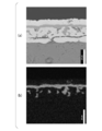
また、本発明例1の電極部の断面を観察した結果を図4に、比較例の電極部の断面を観察した結果を図5に示す。図4及び図5中、(a)がSEM像、(b)がNiマッピング図である。
視野中にサーミスタ素体から電極まで納まるように倍率を設定し、2500倍でSEM‐EDSによる元素マッピング像を撮影した。このマッピング像において、電極表面側でカバー電極層の成分が検出された点からサーミスタ素体までの距離をlとし、視野中でlの最大値をlMAXとした。次に、めっき層の成分が検出された点からサーミスタ素体までの距離をdとし、その最小値をdMINとした。lMAX-dMINの値をめっき層の侵入深さDとした。なお、lMAXを電極部の厚さとした。
また、本発明例1の電極部の断面を観察した結果を図4に、比較例の電極部の断面を観察した結果を図5に示す。図4及び図5中、(a)がSEM像、(b)がNiマッピング図である。
視野中にサーミスタ素体から電極まで納まるように倍率を設定し、2500倍でSEM‐EDSによる元素マッピング像を撮影した。このマッピング像において、電極表面側でカバー電極層の成分が検出された点からサーミスタ素体までの距離をlとし、視野中でlの最大値をlMAXとした。次に、めっき層の成分が検出された点からサーミスタ素体までの距離をdとし、その最小値をdMINとした。lMAX-dMINの値をめっき層の侵入深さDとした。なお、lMAXを電極部の厚さとした。
(電気特性)
25℃における抵抗値の分布(3CV)をめっき前後で比較した。めっき前後の素子を測定用の治具に充てんし、治具ごと防水袋にいれ、25.00℃に調節された恒温水槽に15分間浸漬し、温度が安定した後にデジタルマルチメーターを用いて素子20個の抵抗値を測定した。測定した抵抗値について、不偏分散平方根を平均値で割った変動係数CVを3倍することで、ばらつきの指標としての3CVを算出した。
25℃における抵抗値の分布(3CV)をめっき前後で比較した。めっき前後の素子を測定用の治具に充てんし、治具ごと防水袋にいれ、25.00℃に調節された恒温水槽に15分間浸漬し、温度が安定した後にデジタルマルチメーターを用いて素子20個の抵抗値を測定した。測定した抵抗値について、不偏分散平方根を平均値で割った変動係数CVを3倍することで、ばらつきの指標としての3CVを算出した。
電極部を1層で構成した比較例においては、図5に示すように、Niがサーミスタ素体と電極部との接合界面にまで侵入していた。このため、めっき前後で9%以上の3CVの増加が認められた。サーミスタ素体とめっき液とが接触し、サーミスタ素体が劣化したためと推測される。
これに対して、電極部を2層構造とし、図4に示すように、Niの侵入深さDが電極部の厚さ未満とされた本発明例1-7においては、めっき前後で3CVが大きく変化しておらず、サーミスタ素体の特性が十分に安定していた。
以上のように、本発明例によれば、電極部の表面にめっき層を形成した場合であっても、電極部内部へのめっき液の侵入を抑制でき、サーミスタ素体の特性が安定したサーミスタを製造するサーミスタの製造方法、及び、このサーミスタの製造方法により製造され、特性の安定したサーミスタを提供可能であることが確認された。
10 サーミスタ
11 サーミスタ素体
15 保護膜
20 電極部
21 下地電極層
22 カバー電極層
11 サーミスタ素体
15 保護膜
20 電極部
21 下地電極層
22 カバー電極層
Claims (5)
- サーミスタ素体と、前記サーミスタ素体の端面に形成された電極部と、を備えたサーミスタを製造するサーミスタの製造方法であって、
前記サーミスタ素体の端面に導電性ペーストを塗布して焼成し、下地電極層を形成する下地電極層形成工程と、
前記下地電極層の表面に酸化物層を形成する酸化物層形成工程と、
前記酸化物層の表面に導電性ペーストを塗布して焼成し、カバー電極層を形成するカバー電極層形成工程と、
前記下地電極層と前記カバー電極層とが電気的に導通するように熱処理を行う導通熱処理工程と、
を有し、前記下地電極層と前記カバー電極層とを有する前記電極部を形成するとともに、
前記導通熱処理工程後に、前記カバー電極層の表面に金属めっき層を形成するめっき工程を備えていることを特徴とするサーミスタの製造方法。 - 前記下地電極層形成工程は、金属粉とガラス粉とを含有するガラス入り金属ペーストを塗布して焼成することにより、前記下地電極層を形成することを特徴とする請求項1に記載のサーミスタの製造方法。
- 前記カバー電極層形成工程は、金属粉とガラス粉とを含有するガラス入り金属ペーストを塗布して焼成することにより、前記カバー電極層を形成することを特徴とする請求項1又は請求項2に記載のサーミスタの製造方法。
- 前記酸化物層は、シリコン酸化物で構成されていることを特徴とする請求項1から請求項3のいずれか一項に記載のサーミスタの製造方法。
- サーミスタ素体と、前記サーミスタ素体の端面に形成された電極部と、を備えたサーミスタであって、
前記電極部は、前記サーミスタ素体の端面に形成された下地電極層と、前記下地電極層に積層するカバー電極層と、を備えており、前記電極部の表面に金属めっき層が形成されており、
前記金属めっき層を構成するめっき金属の前記電極部への侵入深さが、前記電極部の厚さ未満とされていることを特徴とするサーミスタ。
Priority Applications (2)
| Application Number | Priority Date | Filing Date | Title |
|---|---|---|---|
| CN202080014059.XA CN113424277A (zh) | 2019-02-15 | 2020-02-05 | 热敏电阻的制造方法及热敏电阻 |
| US17/429,080 US20220139599A1 (en) | 2019-02-15 | 2020-02-05 | Method for manufacturing thermistor, and thermistor |
Applications Claiming Priority (2)
| Application Number | Priority Date | Filing Date | Title |
|---|---|---|---|
| JP2019025313A JP2020136384A (ja) | 2019-02-15 | 2019-02-15 | サーミスタの製造方法、及び、サーミスタ |
| JP2019-025313 | 2019-02-15 |
Publications (1)
| Publication Number | Publication Date |
|---|---|
| WO2020166439A1 true WO2020166439A1 (ja) | 2020-08-20 |
Family
ID=72044687
Family Applications (1)
| Application Number | Title | Priority Date | Filing Date |
|---|---|---|---|
| PCT/JP2020/004213 Ceased WO2020166439A1 (ja) | 2019-02-15 | 2020-02-05 | サーミスタの製造方法、及び、サーミスタ |
Country Status (5)
| Country | Link |
|---|---|
| US (1) | US20220139599A1 (ja) |
| JP (1) | JP2020136384A (ja) |
| CN (1) | CN113424277A (ja) |
| TW (1) | TW202046345A (ja) |
| WO (1) | WO2020166439A1 (ja) |
Families Citing this family (1)
| Publication number | Priority date | Publication date | Assignee | Title |
|---|---|---|---|---|
| WO2022244313A1 (ja) | 2021-05-18 | 2022-11-24 | 株式会社村田製作所 | 電子部品及びその製造方法 |
Citations (2)
| Publication number | Priority date | Publication date | Assignee | Title |
|---|---|---|---|---|
| JPH06295803A (ja) * | 1993-04-07 | 1994-10-21 | Mitsubishi Materials Corp | チップ型サーミスタ及びその製造方法 |
| JP2017199797A (ja) * | 2016-04-27 | 2017-11-02 | Tdk株式会社 | 電子部品 |
Family Cites Families (4)
| Publication number | Priority date | Publication date | Assignee | Title |
|---|---|---|---|---|
| US5339068A (en) * | 1992-12-18 | 1994-08-16 | Mitsubishi Materials Corp. | Conductive chip-type ceramic element and method of manufacture thereof |
| JP2003068508A (ja) * | 2001-08-24 | 2003-03-07 | Murata Mfg Co Ltd | 積層チップバリスタの製造方法 |
| CN2501164Y (zh) * | 2001-09-26 | 2002-07-17 | 成都宏明电子股份有限公司 | 单层片式热敏电阻器 |
| TWI628678B (zh) * | 2016-04-21 | 2018-07-01 | Tdk 股份有限公司 | 電子零件 |
-
2019
- 2019-02-15 JP JP2019025313A patent/JP2020136384A/ja active Pending
-
2020
- 2020-02-05 CN CN202080014059.XA patent/CN113424277A/zh active Pending
- 2020-02-05 WO PCT/JP2020/004213 patent/WO2020166439A1/ja not_active Ceased
- 2020-02-05 US US17/429,080 patent/US20220139599A1/en not_active Abandoned
- 2020-02-10 TW TW109104005A patent/TW202046345A/zh unknown
Patent Citations (2)
| Publication number | Priority date | Publication date | Assignee | Title |
|---|---|---|---|---|
| JPH06295803A (ja) * | 1993-04-07 | 1994-10-21 | Mitsubishi Materials Corp | チップ型サーミスタ及びその製造方法 |
| JP2017199797A (ja) * | 2016-04-27 | 2017-11-02 | Tdk株式会社 | 電子部品 |
Also Published As
| Publication number | Publication date |
|---|---|
| US20220139599A1 (en) | 2022-05-05 |
| TW202046345A (zh) | 2020-12-16 |
| CN113424277A (zh) | 2021-09-21 |
| JP2020136384A (ja) | 2020-08-31 |
Similar Documents
| Publication | Publication Date | Title |
|---|---|---|
| JP3555563B2 (ja) | 積層チップバリスタの製造方法および積層チップバリスタ | |
| US9959975B2 (en) | Ceramic electronic component | |
| CN104969307B (zh) | 陶瓷电子部件及其制造方法 | |
| KR101741132B1 (ko) | 세라믹 전자 부품 및 그 제조 방법 | |
| JP5142090B2 (ja) | セラミック積層電子部品およびその製造方法 | |
| CN104871270B (zh) | 层叠陶瓷电子部件及其制造方法 | |
| JP4506066B2 (ja) | チップ型電子部品及びチップ型電子部品の製造方法 | |
| JPWO2009096333A1 (ja) | チップ型半導体セラミック電子部品 | |
| JP7534987B2 (ja) | セラミック電子部品 | |
| JP7268393B2 (ja) | サーミスタの製造方法 | |
| US20220139599A1 (en) | Method for manufacturing thermistor, and thermistor | |
| JP2016063079A (ja) | 抵抗素子およびその製造方法 | |
| WO2023140054A1 (ja) | サーミスタ素子及びその製造方法 | |
| TW202019822A (zh) | 熱敏電阻及熱敏電阻之製造方法 | |
| JPH10144501A (ja) | チップ抵抗器及びその製造方法 | |
| JPH08236306A (ja) | チップ型サーミスタとその製造方法 | |
| JP2003068508A (ja) | 積層チップバリスタの製造方法 | |
| JP2011151250A (ja) | 電子部品および電子部品の製造方法 | |
| JP2012216699A (ja) | チップptcサーミスタ | |
| JP2010040560A (ja) | チップ型ptcサーミスタおよびその製造方法 | |
| JPWO2015198615A1 (ja) | Ptcサーミスタおよびその製造方法 |
Legal Events
| Date | Code | Title | Description |
|---|---|---|---|
| 121 | Ep: the epo has been informed by wipo that ep was designated in this application |
Ref document number: 20755047 Country of ref document: EP Kind code of ref document: A1 |
|
| NENP | Non-entry into the national phase |
Ref country code: DE |
|
| 122 | Ep: pct application non-entry in european phase |
Ref document number: 20755047 Country of ref document: EP Kind code of ref document: A1 |