WO2020162464A1 - 感光性樹脂組成物、感光性エレメント、レジストパターンの形成方法及びプリント配線板の製造方法 - Google Patents
感光性樹脂組成物、感光性エレメント、レジストパターンの形成方法及びプリント配線板の製造方法 Download PDFInfo
- Publication number
- WO2020162464A1 WO2020162464A1 PCT/JP2020/004182 JP2020004182W WO2020162464A1 WO 2020162464 A1 WO2020162464 A1 WO 2020162464A1 JP 2020004182 W JP2020004182 W JP 2020004182W WO 2020162464 A1 WO2020162464 A1 WO 2020162464A1
- Authority
- WO
- WIPO (PCT)
- Prior art keywords
- resin composition
- photosensitive resin
- photosensitive
- meth
- mass
- Prior art date
- Legal status (The legal status is an assumption and is not a legal conclusion. Google has not performed a legal analysis and makes no representation as to the accuracy of the status listed.)
- Ceased
Links
Classifications
-
- G—PHYSICS
- G03—PHOTOGRAPHY; CINEMATOGRAPHY; ANALOGOUS TECHNIQUES USING WAVES OTHER THAN OPTICAL WAVES; ELECTROGRAPHY; HOLOGRAPHY
- G03F—PHOTOMECHANICAL PRODUCTION OF TEXTURED OR PATTERNED SURFACES, e.g. FOR PRINTING, FOR PROCESSING OF SEMICONDUCTOR DEVICES; MATERIALS THEREFOR; ORIGINALS THEREFOR; APPARATUS SPECIALLY ADAPTED THEREFOR
- G03F7/00—Photomechanical, e.g. photolithographic, production of textured or patterned surfaces, e.g. printing surfaces; Materials therefor, e.g. comprising photoresists; Apparatus specially adapted therefor
- G03F7/004—Photosensitive materials
- G03F7/027—Non-macromolecular photopolymerisable compounds having carbon-to-carbon double bonds, e.g. ethylenic compounds
- G03F7/028—Non-macromolecular photopolymerisable compounds having carbon-to-carbon double bonds, e.g. ethylenic compounds with photosensitivity-increasing substances, e.g. photoinitiators
-
- C—CHEMISTRY; METALLURGY
- C08—ORGANIC MACROMOLECULAR COMPOUNDS; THEIR PREPARATION OR CHEMICAL WORKING-UP; COMPOSITIONS BASED THEREON
- C08F—MACROMOLECULAR COMPOUNDS OBTAINED BY REACTIONS ONLY INVOLVING CARBON-TO-CARBON UNSATURATED BONDS
- C08F2/00—Processes of polymerisation
- C08F2/44—Polymerisation in the presence of compounding ingredients, e.g. plasticisers, dyestuffs, fillers
-
- C—CHEMISTRY; METALLURGY
- C08—ORGANIC MACROMOLECULAR COMPOUNDS; THEIR PREPARATION OR CHEMICAL WORKING-UP; COMPOSITIONS BASED THEREON
- C08F—MACROMOLECULAR COMPOUNDS OBTAINED BY REACTIONS ONLY INVOLVING CARBON-TO-CARBON UNSATURATED BONDS
- C08F2/00—Processes of polymerisation
- C08F2/46—Polymerisation initiated by wave energy or particle radiation
- C08F2/48—Polymerisation initiated by wave energy or particle radiation by ultraviolet or visible light
- C08F2/50—Polymerisation initiated by wave energy or particle radiation by ultraviolet or visible light with sensitising agents
-
- C—CHEMISTRY; METALLURGY
- C08—ORGANIC MACROMOLECULAR COMPOUNDS; THEIR PREPARATION OR CHEMICAL WORKING-UP; COMPOSITIONS BASED THEREON
- C08F—MACROMOLECULAR COMPOUNDS OBTAINED BY REACTIONS ONLY INVOLVING CARBON-TO-CARBON UNSATURATED BONDS
- C08F257/00—Macromolecular compounds obtained by polymerising monomers on to polymers of aromatic monomers as defined in group C08F12/00
- C08F257/02—Macromolecular compounds obtained by polymerising monomers on to polymers of aromatic monomers as defined in group C08F12/00 on to polymers of styrene or alkyl-substituted styrenes
-
- C—CHEMISTRY; METALLURGY
- C08—ORGANIC MACROMOLECULAR COMPOUNDS; THEIR PREPARATION OR CHEMICAL WORKING-UP; COMPOSITIONS BASED THEREON
- C08F—MACROMOLECULAR COMPOUNDS OBTAINED BY REACTIONS ONLY INVOLVING CARBON-TO-CARBON UNSATURATED BONDS
- C08F265/00—Macromolecular compounds obtained by polymerising monomers on to polymers of unsaturated monocarboxylic acids or derivatives thereof as defined in group C08F20/00
- C08F265/04—Macromolecular compounds obtained by polymerising monomers on to polymers of unsaturated monocarboxylic acids or derivatives thereof as defined in group C08F20/00 on to polymers of esters
- C08F265/06—Polymerisation of acrylate or methacrylate esters on to polymers thereof
-
- C—CHEMISTRY; METALLURGY
- C08—ORGANIC MACROMOLECULAR COMPOUNDS; THEIR PREPARATION OR CHEMICAL WORKING-UP; COMPOSITIONS BASED THEREON
- C08F—MACROMOLECULAR COMPOUNDS OBTAINED BY REACTIONS ONLY INVOLVING CARBON-TO-CARBON UNSATURATED BONDS
- C08F290/00—Macromolecular compounds obtained by polymerising monomers on to polymers modified by introduction of aliphatic unsaturated end or side groups
- C08F290/02—Macromolecular compounds obtained by polymerising monomers on to polymers modified by introduction of aliphatic unsaturated end or side groups on to polymers modified by introduction of unsaturated end groups
- C08F290/06—Polymers provided for in subclass C08G
-
- G—PHYSICS
- G03—PHOTOGRAPHY; CINEMATOGRAPHY; ANALOGOUS TECHNIQUES USING WAVES OTHER THAN OPTICAL WAVES; ELECTROGRAPHY; HOLOGRAPHY
- G03F—PHOTOMECHANICAL PRODUCTION OF TEXTURED OR PATTERNED SURFACES, e.g. FOR PRINTING, FOR PROCESSING OF SEMICONDUCTOR DEVICES; MATERIALS THEREFOR; ORIGINALS THEREFOR; APPARATUS SPECIALLY ADAPTED THEREFOR
- G03F7/00—Photomechanical, e.g. photolithographic, production of textured or patterned surfaces, e.g. printing surfaces; Materials therefor, e.g. comprising photoresists; Apparatus specially adapted therefor
- G03F7/004—Photosensitive materials
-
- G—PHYSICS
- G03—PHOTOGRAPHY; CINEMATOGRAPHY; ANALOGOUS TECHNIQUES USING WAVES OTHER THAN OPTICAL WAVES; ELECTROGRAPHY; HOLOGRAPHY
- G03F—PHOTOMECHANICAL PRODUCTION OF TEXTURED OR PATTERNED SURFACES, e.g. FOR PRINTING, FOR PROCESSING OF SEMICONDUCTOR DEVICES; MATERIALS THEREFOR; ORIGINALS THEREFOR; APPARATUS SPECIALLY ADAPTED THEREFOR
- G03F7/00—Photomechanical, e.g. photolithographic, production of textured or patterned surfaces, e.g. printing surfaces; Materials therefor, e.g. comprising photoresists; Apparatus specially adapted therefor
- G03F7/004—Photosensitive materials
- G03F7/027—Non-macromolecular photopolymerisable compounds having carbon-to-carbon double bonds, e.g. ethylenic compounds
- G03F7/032—Non-macromolecular photopolymerisable compounds having carbon-to-carbon double bonds, e.g. ethylenic compounds with binders
- G03F7/033—Non-macromolecular photopolymerisable compounds having carbon-to-carbon double bonds, e.g. ethylenic compounds with binders the binders being polymers obtained by reactions only involving carbon-to-carbon unsaturated bonds, e.g. vinyl polymers
-
- G—PHYSICS
- G03—PHOTOGRAPHY; CINEMATOGRAPHY; ANALOGOUS TECHNIQUES USING WAVES OTHER THAN OPTICAL WAVES; ELECTROGRAPHY; HOLOGRAPHY
- G03F—PHOTOMECHANICAL PRODUCTION OF TEXTURED OR PATTERNED SURFACES, e.g. FOR PRINTING, FOR PROCESSING OF SEMICONDUCTOR DEVICES; MATERIALS THEREFOR; ORIGINALS THEREFOR; APPARATUS SPECIALLY ADAPTED THEREFOR
- G03F7/00—Photomechanical, e.g. photolithographic, production of textured or patterned surfaces, e.g. printing surfaces; Materials therefor, e.g. comprising photoresists; Apparatus specially adapted therefor
- G03F7/20—Exposure; Apparatus therefor
-
- H—ELECTRICITY
- H05—ELECTRIC TECHNIQUES NOT OTHERWISE PROVIDED FOR
- H05K—PRINTED CIRCUITS; CASINGS OR CONSTRUCTIONAL DETAILS OF ELECTRIC APPARATUS; MANUFACTURE OF ASSEMBLAGES OF ELECTRICAL COMPONENTS
- H05K3/00—Apparatus or processes for manufacturing printed circuits
- H05K3/02—Apparatus or processes for manufacturing printed circuits in which the conductive material is applied to the surface of the insulating support and is thereafter removed from such areas of the surface which are not intended for current conducting or shielding
- H05K3/06—Apparatus or processes for manufacturing printed circuits in which the conductive material is applied to the surface of the insulating support and is thereafter removed from such areas of the surface which are not intended for current conducting or shielding the conductive material being removed chemically or electrolytically, e.g. by photo-etch process
-
- H—ELECTRICITY
- H05—ELECTRIC TECHNIQUES NOT OTHERWISE PROVIDED FOR
- H05K—PRINTED CIRCUITS; CASINGS OR CONSTRUCTIONAL DETAILS OF ELECTRIC APPARATUS; MANUFACTURE OF ASSEMBLAGES OF ELECTRICAL COMPONENTS
- H05K3/00—Apparatus or processes for manufacturing printed circuits
- H05K3/10—Apparatus or processes for manufacturing printed circuits in which conductive material is applied to the insulating support in such a manner as to form the desired conductive pattern
- H05K3/18—Apparatus or processes for manufacturing printed circuits in which conductive material is applied to the insulating support in such a manner as to form the desired conductive pattern using precipitation techniques to apply the conductive material
-
- H—ELECTRICITY
- H10—SEMICONDUCTOR DEVICES; ELECTRIC SOLID-STATE DEVICES NOT OTHERWISE PROVIDED FOR
- H10P—GENERIC PROCESSES OR APPARATUS FOR THE MANUFACTURE OR TREATMENT OF DEVICES COVERED BY CLASS H10
- H10P76/00—Manufacture or treatment of masks on semiconductor bodies, e.g. by lithography or photolithography
Definitions
- the present invention relates to a photosensitive resin composition, a photosensitive element, a resist pattern forming method, and a printed wiring board manufacturing method.
- a photosensitive resin composition As a resist material used for etching treatment, plating treatment, etc., a photosensitive resin composition, and a support and a layer formed using the photosensitive resin composition on the support ( Hereinafter, a photosensitive element (laminate) including a "photosensitive layer”) is widely used.
- a printed wiring board using a photosensitive element When manufacturing a printed wiring board using a photosensitive element, first laminate the photosensitive layer of the photosensitive element on the circuit-forming board. Next, after peeling and removing the support, an actinic ray is irradiated to a predetermined portion of the photosensitive layer to cure the exposed portion. After that, a resist pattern is formed on the substrate by removing the unexposed portion of the photosensitive layer with a developing solution. Next, using this resist pattern as a mask, the substrate on which the resist pattern has been formed is subjected to etching or plating to form a circuit pattern on the substrate, and finally the cured portion (resist pattern) of the photosensitive layer is peeled off from the substrate. Remove.
- the photosensitive resin layer is pattern-exposed through a mask film or the like.
- a projection exposure method has been used in which an actinic ray on which an image of a photomask is projected is applied to a photosensitive resin layer through a lens to expose the active layer.
- An ultra-high pressure mercury lamp is used as a light source used in the projection exposure method.
- an exposing machine using i-ray monochromatic light (365 nm) as an exposure wavelength is often used, but an exposure wavelength of h-ray monochromatic light (405 nm) or ihg mixed line may also be used.
- the projection exposure method is an exposure method that can ensure higher resolution and higher alignment than the contact exposure method. For this reason, the projection exposure method has received a great deal of attention in these days when miniaturization of circuit formation in a printed wiring board is required.
- the photosensitive resin composition has a finer resist pattern having a line width and a space width of 5 ⁇ m or less, and a line width and a space width of 1 ⁇ m or less. Is desired to be formed.
- the present disclosure has been made in view of the problems of the above-described conventional technology, is excellent in resolution and adhesion, and is a photosensitive resin composition capable of forming a fine resist pattern, and a photosensitive resin composition using the same.
- An object is to provide an element, a method for forming a resist pattern, and a method for manufacturing a printed wiring board.
- One aspect of the present disclosure is a photosensitive resin composition containing a binder polymer, a photopolymerizable compound, and a photopolymerization initiator, wherein the binder polymer has a dicyclopentanyl group (meth).
- the present invention relates to a photosensitive resin composition containing a structural unit derived from an acrylate compound.
- the content of the structural unit derived from the (meth)acrylate compound having a dicyclopentanyl group is 1 to 50 mass based on the total mass of the structural units derived from the polymerizable monomer constituting the binder polymer. May be %.
- the above photosensitive resin composition may further contain a sensitizing dye having an absorption maximum at 340 nm to 430 nm.
- Another aspect of the present disclosure also relates to a photosensitive element including a support and a photosensitive layer formed on the support using the photosensitive resin composition.
- Another aspect of the present disclosure is also a photosensitive layer forming step of laminating a photosensitive layer containing the photosensitive resin composition, or the photosensitive layer of the photosensitive element on a substrate, and an actinic ray to a predetermined portion of the photosensitive layer.
- the present invention relates to a method for forming a resist pattern, which includes an exposure step of irradiating to form a photo-cured portion and a developing step of removing a region other than a predetermined portion of a photosensitive layer from a substrate.
- Another aspect of the present disclosure also relates to a method for manufacturing a printed wiring board, including a step of forming a conductor pattern by etching or plating a substrate on which a resist pattern has been formed by the above method for forming a resist pattern. ..
- a photosensitive resin composition having excellent resolution and adhesiveness and capable of forming a fine resist pattern, a photosensitive element using the same, a method for forming a resist pattern, and manufacturing of a printed wiring board.
- a method can be provided.
- the term “step” is included in this term as long as the intended action of the step is achieved not only as an independent step but also when it cannot be clearly distinguished from other steps. Be done.
- the term “layer” includes not only the structure of the shape formed on the entire surface but also the structure of the shape partially formed when observed as a plan view.
- (meth)acrylic acid means at least one of “acrylic acid” and “methacrylic acid” corresponding thereto. The same applies to other similar expressions such as (meth)acrylate.
- the numerical range indicated by using “to” indicates the range including the numerical values before and after “to” as the minimum value and the maximum value, respectively.
- the upper limit value or the lower limit value of the numerical range of a certain stage may be replaced with the upper limit value or the lower limit value of the numerical range of another stage.
- the upper limit value or the lower limit value of the numerical range may be replaced with the value shown in the examples.
- the amount of each component in the composition when there are a plurality of substances corresponding to each component in the composition, the plurality of substances present in the composition unless otherwise specified. Means the total amount of.
- the photosensitive resin composition of the present embodiment contains (A) component: binder polymer, (B) component: photopolymerizable compound, and (C) component: photopolymerization initiator.
- the binder polymer includes a structural unit derived from a (meth)acrylate compound having a dicyclopentanyl group.
- the photosensitive resin composition may further contain (D) component: a sensitizing dye having an absorption maximum at 340 nm to 430 nm, a hydrogen donor or other components, if necessary.
- D component: a sensitizing dye having an absorption maximum at 340 nm to 430 nm, a hydrogen donor or other components, if necessary.
- component (C) binder polymer
- the photosensitive resin composition of the present embodiment by containing the components (A) to (C), it is possible to form a fine resist pattern with excellent resolution and adhesion.
- the use of a binder polymer containing a structural unit derived from a (meth)acrylate compound having a dicyclopentanyl group could improve the resolution and the adhesion.
- the component (A) can be produced, for example, by radically polymerizing a polymerizable monomer containing a (meth)acrylate compound having a dicyclopentanyl group.
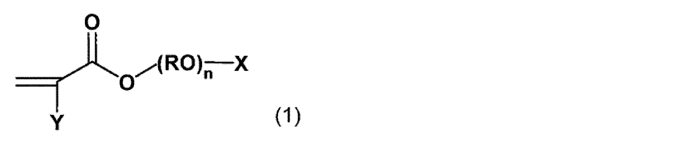
- a compound represented by the following formula (1) may be used as the (meth)acrylate compound having a dicyclopentanyl group.
- Y represents a hydrogen atom or a methyl group
- R represents an alkylene group having 1 to 4 carbon atoms
- X represents a dicyclopentanyl group
- n represents an integer of 0 to 2. Show.
- Examples of the (meth)acrylate compound having a dicyclopentanyl group include dicyclopentanyl (meth)acrylate, dicyclopentanyloxyethyl (meth)acrylate, and dicyclopentanyloxypropyl (meth)acrylate. , And dicyclopentanyloxypropyloxyethyl (meth)acrylate. From the viewpoint of further increasing the hydrophobicity of the binder polymer, dicyclopentanyl (meth)acrylate may be used.
- a structural unit derived from a (meth)acrylate compound having a dicyclopentanyl group (hereinafter, also referred to as “dicyclopentanyl-based structural unit”). Content of 1) to 50% by mass, 3 to 40% by mass, 5 to 30% by mass based on the total mass of the structural units derived from the polymerizable monomer constituting the binder polymer (100% by mass). It may be% by weight, or 6-25% by weight.
- the component (A) may further include a structural unit derived from (meth)acrylic acid, and from the viewpoint of improving the resolution and adhesion and reducing the amount of resist skirts generated, It may further include a structural unit derived from styrene or a styrene derivative (hereinafter, also referred to as “styrene-based structural unit”).
- a compound represented by the following formula (2) may be used as styrene or a styrene derivative.
- R 11 represents a hydrogen atom or a methyl group
- R 12 independently represents a hydrogen atom, an alkyl group, a (meth)acryloyl group, a phenyl group or a derivative thereof
- n is an integer of 1 to 5.
- styrene derivative examples include vinyltoluene, ⁇ -methylstyrene, p-methylstyrene, and p-ethylstyrene.
- the content of the dicyclopentanyl structural unit and the styrene structural unit is derived from the polymerizable monomer that constitutes the binder polymer. It may be 50% by mass or more, 55% by mass or more, or 58% by mass or more based on the total mass of the structural unit.
- the content of the dicyclopentanyl-based structural unit and the styrene-based structural unit is 85% by mass or less, 80% by mass or less, or 75% by mass or less from the viewpoint that the development time is appropriately shortened and the residual development is less likely to occur. May be
- the content of the structural unit derived from (meth)acrylic acid is derived from the polymerizable monomer that constitutes the binder polymer, from the viewpoint of improving the resolution, adhesion, and suppression of resist skirt generation. It may be 10-40% by weight, 15-35% by weight, or 20-30% by weight, based on the total weight of the structural units.
- the component (A) may further include a structural unit derived from a polymerizable monomer other than the above (hereinafter also referred to as “other monomer”).
- other monomer examples include benzyl (meth)acrylate or a derivative thereof, cycloalkyl (meth)acrylate, furfuryl (meth)acrylate, tetrahydrofurfuryl (meth)acrylate, and isobornyl (meth)acrylate.
- the weight average molecular weight (Mw) of the component (A) may be 10,000 to 80,000, 15,000 to 70,000, 20,000 to 50,000, 23,000 to 40,000, or 25,000 to 35,000. When Mw is 80,000 or less, resolution and developability tend to be improved, and when Mw is 10,000 or more, flexibility of the cured film is improved and chipping and peeling of a resist pattern are less likely to occur. There is a tendency.
- the dispersity (Mw/Mn) of the component (A) may be 1.0 to 3.0, or 1.0 to 2.3. The resolution tends to improve as the degree of dispersion decreases.
- the weight average molecular weight of the binder polymer is measured by gel permeation chromatography (GPC) (converted by a calibration curve using standard polystyrene).
- the acid value of the component (A) may be 100 to 250 mgKOH/g, 120 to 240 mgKOH/g, 140 to 230 mgKOH/g, or 150 to 230 mgKOH/g.
- the acid value of the component (A) is 100 mgKOH/g or more, it is possible to sufficiently suppress the development time from becoming long, and when it is 250 mgKOH/g or less, the developer resistance of the cured product of the photosensitive resin composition is high. It becomes easy to improve the property (adhesion).
- the acid value of the component (A) can be measured as follows. First, 1 g of a binder polymer whose acid value is to be measured is precisely weighed. 30 g of acetone is added to the precisely weighed binder polymer, and this is uniformly dissolved. Next, an appropriate amount of phenolphthalein, which is an indicator, is added to the solution, and titration is performed using a 0.1N potassium hydroxide (KOH) aqueous solution. The acid value is determined by calculating the mg number of KOH required to neutralize the acetone solution of the binder polymer that is the measurement target.
- KOH potassium hydroxide
- Vf represents the titration amount (mL) of the KOH aqueous solution
- Wp represents the measured mass (g) of the solution containing the binder polymer
- I represents the ratio of the nonvolatile content in the solution containing the measured binder polymer. (Mass %) is shown.
- the binder polymer When the binder polymer is mixed in a state where it is mixed with volatile components such as a synthetic solvent and a diluting solvent, it is volatilized by heating at a temperature higher than the boiling point of volatile components by 10° C. or more for 1 to 4 hours before the precise weighing.
- volatile components such as a synthetic solvent and a diluting solvent
- the acid value can be measured after removing the components.
- one type of binder polymer may be used alone, or two or more types of binder polymers may be used in any combination.
- the binder polymer in the case of using two or more kinds in combination include, for example, two or more kinds of binder polymers composed of different copolymerization components (containing different monomer units as copolymerization components), and two or more kinds of binder polymers having different Mw. , Two or more binder polymers having different dispersities.
- the content of the component (A) in the photosensitive resin composition of the present embodiment is 20 to 90% by mass, 30 to 80% by mass, or 40 to 65% by mass based on the total solid content of the photosensitive resin composition. May be When the content of the component (A) is 20% by mass or more, the film moldability tends to be excellent, and when it is 90% by mass or less, the sensitivity and resolution tend to be excellent.
- the component (B) is not particularly limited as long as it is a photopolymerizable compound having at least one ethylenically unsaturated bond.
- the component (B) preferably contains at least one bisphenol-type (meth)acrylate from the viewpoint of improving alkali developability, resolution, and peeling properties after curing, and the bisphenol-type (meth)acrylate Above all, it is more preferable to contain bisphenol A type (meth)acrylate.
- the bisphenol A type (meth)acrylate include 2,2-bis(4-((meth)acryloxypolyethoxy)phenyl)propane and 2,2-bis(4-((meth)acryloxypolypropoxy).
- Phenyl)propane 2,2-bis(4-((meth)acryloxypolybutoxy)phenyl)propane, and 2,2-bis(4-((meth)acryloxypolyethoxypolypropoxy)phenyl)propane.
- 2,2-bis(4-((meth)acryloxypolyethoxy)phenyl)propane is preferable from the viewpoint of further improving the resolution and the peeling property.
- commercially available products include, for example, 2,2-bis(4-((meth)acryloxydipropoxy)phenyl)propane, which is BPE-200 (Shin-Nakamura Chemical Co., Ltd.).
- BPE-200 Shin-Nakamura Chemical Co., Ltd.
- BPE-500 Shin-Nakamura Chemical Co., Ltd.
- FA-321M Heitachi Chemical Co., Ltd.
- the refractive index of BPE-200 is 1.512
- the refractive index of BPE-500 is 1.532.
- the content of the bisphenol type (meth)acrylate may be 40 to 98% by mass, 50 to 97% by mass, 60 to 95% by mass, or 70 to 90% by mass based on the total amount of the component (B). ..
- the content is 40% by mass or more, the resolution, adhesion, and resist skirt generation suppression property are better, and when the content is 98% by mass or less, the development time is appropriately shortened, and the development The rest is less likely to occur.
- the component (B) other than the bisphenol type (meth)acrylate from the viewpoint of improving the flexibility of the cured product (cured film), at least one of a (poly)oxyethylene chain and a (poly)oxypropylene chain in the molecule.
- the content of the polyalkylene glycol di(meth)acrylate may be 2 to 40% by mass, 3 to 30% by mass, or 5 to 20% by mass based on the total mass of the component (B).
- polyalkylene glycol di(meth)acrylate examples include FA-023M (manufactured by Hitachi Chemical Co., Ltd., trade name), FA-024M (manufactured by Hitachi Chemical Co., Ltd., trade name), and NK ester HEMA-9P. (Shin-Nakamura Chemical Co., Ltd., trade name). You may use these individually by 1 type or in combination of 2 or more types.
- nonylphenoxy polyethyleneoxy acrylate, phthalic acid compound, (meth)acrylic acid polyol ester, (meth)acrylic acid alkyl ester and the like may be used.
- the component (B) contains at least one selected from nonylphenoxy polyethyleneoxy acrylate and a phthalic acid compound from the viewpoint of improving the balance of the resolution, adhesion, resist shape and peeling property after curing. Good.
- the content thereof is 5 to 50% by mass, 5 to 40% by mass in the total mass of the component (B) from the viewpoint of improving the resolution. Alternatively, it may be 10 to 30% by mass.
- nonylphenoxypolyethyleneoxy acrylate examples include nonylphenoxytriethyleneoxyacrylate, nonylphenoxytetraethyleneoxyacrylate, nonylphenoxypentaethyleneoxyacrylate, nonylphenoxyhexaethyleneoxyacrylate, nonylphenoxyheptaethyleneoxyacrylate, nonylphenoxyoctaethyleneoxyacrylate.
- Examples of the phthalic acid compound include ⁇ -chloro- ⁇ -hydroxypropyl- ⁇ ′-(meth)acryloyloxyethyl-o-phthalate and ⁇ -hydroxyethyl- ⁇ ′-(meth)acryloyloxyethyl-o-phthalate. , And ⁇ -hydroxypropyl- ⁇ ′-(meth)acryloyloxyethyl-o-phthalate, among which ⁇ -chloro- ⁇ -hydroxypropyl- ⁇ ′-(meth)acryloyloxyethyl-o-phthalate. May be.
- ⁇ -Chloro- ⁇ -hydroxypropyl- ⁇ '-methacryloyloxyethyl-o-phthalate is commercially available as FA-MECH (trade name, manufactured by Hitachi Chemical Co., Ltd.).
- the component (B) may include (meth)acrylic acid polyol.
- the (meth)acrylic acid polyol ester include trimethylolpropane polyethoxytri(meth)acrylate, trimethylolpropane polypropoxytri(meth)acrylate, trimethylolpropane polybutoxytri(meth)acrylate, trimethylolpropane polyethoxy.
- the content of the component (B) is preferably 20 to 60 parts by mass, more preferably 30 to 55 parts by mass, based on 100 parts by mass of the total amount of the components (A) and (B). More preferably, it is from 35 to 50 parts by mass.
- the content of the component (B) is in this range, the photosensitivity and the coating property are further improved in addition to the resolution and adhesiveness of the photosensitive resin composition and the resist skirt generation property.
- Component (C) photopolymerization initiator
- the component (C) is not particularly limited, but a hexaarylbiimidazole derivative or an acridine compound having one or more acridinyl groups may be used from the viewpoint of improving the balance of sensitivity and resolution.
- the component (C) may contain an acridine compound having one or more acridinyl groups, from the viewpoint of sensitivity and adhesion.
- hexaarylbiimidazole derivative examples include 2-(o-chlorophenyl)-4,5-diphenylbiimidazole and 2,2',5-tris-(o-chlorophenyl)-4-(3,4-dimethoxyphenyl).
- 2-(o-chlorophenyl)-4,5-diphenylimidazole dimer is preferable from the viewpoint of sensitivity and resolution.
- 2-(o-chlorophenyl)-4,5-diphenylimidazole dimer includes 2,2'-bis(2-chlorophenyl)-4,4',5,5'-tetraphenyl-1,2-bi Imidazole is commercially available under the trade name “B-CIM” manufactured by Hodogaya Chemical Co., Ltd.
- acridine compound examples include 9-phenylacridine, 9-(p-methylphenyl)acridine, 9-(m-methylphenyl)acridine, 9-(p-chlorophenyl)acridine, 9-(m-chlorophenyl)acridine, 9-aminoacridine, 9-dimethylaminoacridine, 9-diethylaminoacridine, 9-pentylaminoacridine, 1,2-bis(9-acridinyl)ethane, 1,4-bis(9-acridinyl)butane, 1,6- Bis(9-acridinyl)hexane, 1,8-bis(9-acridinyl)octane, 1,10-bis(9-acridinyl)decane, 1,12-bis(9-acridinyl)dodecane, 1,14-bis( Bis(9-acridinyl)alkane
- photopolymerization initiators include, for example, benzophenones such as 4,4′-bis(diethylamino)benzophenone; 2-benzyl-2-dimethylamino-1-(4-morpholinophenyl)-butanone-1,2- Aromatic ketones such as methyl-1-[4-(methylthio)phenyl]-2-morpholino-propanone-1; quinones such as alkylanthraquinones; benzoin ether compounds such as benzoin alkyl ethers; benzoin compounds such as benzoin and alkylbenzoins Benzyl derivatives such as benzyl dimethyl ketal, N-phenylglycine, N-phenylglycine derivatives; 2,4,6-trimethylbenzoyl-diphenyl-phosphine oxide, bis(2,4,6-trimethylbenzoyl)-phenylphosphine Acylphosphine oxide-based photopolymerization initiators such as oxides; 1,
- the content of the component (C) may be 0.1 to 10% by mass, 1 to 5% by mass, or 2 to 4.5% by mass based on the total solid content of the photosensitive resin composition.
- the content of the component (C) is within the above range, it tends to be easy to improve both photosensitivity and resolution in a well-balanced manner.
- the content of the component (C) is 0.5 to 10 parts by mass and 1 to 8 parts by mass based on 100 parts by mass of the total amount of the components (A) and (B). It may be parts by weight, or 1.5 to 5 parts by weight.
- the photosensitive resin composition of this embodiment may further contain a sensitizer. This further improves the photosensitivity of the photosensitive resin composition.
- the sensitizer include dialkylaminobenzophenone compounds, pyrazoline compounds, anthracene compounds, coumarin compounds, xanthone compounds, oxazole compounds, benzoxazole compounds, thiazole compounds, benzothiazole compounds, triazole compounds, stilbene compounds, triazine compounds, thiophene compounds. , Naphthalimide compounds, and triarylamine compounds. These are used alone or in combination of two or more.
- the component (D) may contain a sensitizing dye having an absorption maximum at 340 to 430 nm.
- At least one selected from the group consisting of a pyrazoline compound, an anthracene compound, a coumarin compound and a triarylamine compound is selected from the viewpoint of sensitivity and adhesion.
- it may contain at least one selected from the group consisting of a pyrazoline compound, an anthracene compound and a triarylamine compound.
- the content of the component (D) is 0.01 to 10% by mass and 0.05 to 5% by mass based on the total solid content of the photosensitive resin composition. It may be mass %, or 0.1 to 3 mass %.
- the content of the component (D) is 0.01% by mass or more, the sensitivity and resolution are further improved, and when it is 10% by mass or less, the resist shape is prevented from becoming an inverted trapezoid. , The adhesion is further improved.
- the content of the component (D) is 0.05 to 5 parts by mass, 0.1 to 5 parts by mass based on 100 parts by mass of the total amount of the components (A) and (B). It may be parts by weight, or 0.5 to 3 parts by weight.
- the photosensitive resin composition may further contain a hydrogen donor. This further improves the sensitivity of the photosensitive resin composition.
- hydrogen donors include bis[4-(dimethylamino)phenyl]methane, bis[4-(diethylamino)phenyl]methane, N-phenylglycine, and leuco crystal violet. These are used alone or in combination of two or more.
- the photosensitive resin composition contains a hydrogen donor
- the content thereof is 0.01 to 10% by mass, 0.05 to 5% by mass, or 0.1% by mass based on the total solid content of the photosensitive resin composition. It may be 1 to 2% by mass.
- the content of the hydrogen donor is 0.01% by mass or more, the sensitivity can be further improved, and when the content is 10% by mass or less, an excessive hydrogen donor can be deposited as a foreign substance after the film formation. Suppressed.
- the photosensitive resin composition may further contain other components, if necessary.
- Other components include, for example, a photopolymerizable compound (oxetane compound or the like) having at least one cationically polymerizable cyclic ether group in the molecule, a cationic polymerization initiator, a dye (malachite green or the like), tribromophenyl sulfone, Photo-coloring agent, thermal coloring inhibitor, plasticizer (p-toluenesulfonamide, etc.), polymerization inhibitor (tert-butylcatechol, etc.), silane coupling agent, pigment, filler, defoaming agent, flame retardant, stabilizer Adhesion imparting agents (benzotriazole and the like), leveling agents, peeling accelerators, antioxidants, fragrances, imaging agents, thermal crosslinking agents and the like. These are used alone or in combination of two or more.
- the content of each of the other components may be about 0.01 to 20% by mass.
- the photosensitive resin composition may contain at least one organic solvent in order to improve the handling property of the photosensitive composition and adjust the viscosity and storage stability.
- the organic solvent a commonly used organic solvent can be used without particular limitation.
- the organic solvent include methanol, ethanol, acetone, methyl ethyl ketone, methyl cellosolve, ethyl cellosolve, toluene, N,N-dimethylformamide, propylene glycol monomethyl ether, and mixed solvents thereof.
- the component (A), the component (B), and the component (C) are dissolved in an organic solvent and used as a solution having a solid content of about 30 to 60% by mass (hereinafter referred to as “coating liquid”). You can In addition, solid content means the remaining component except the volatile component from the solution of the photosensitive resin composition.
- the photosensitive element of the present embodiment includes a support and a photosensitive layer formed on the support and containing the photosensitive resin composition.
- the photosensitive layer may be laminated on the substrate and then exposed without peeling the support.
- a polymer film (support film) having heat resistance and solvent resistance such as polyester such as polyethylene terephthalate (PET), polyolefin such as polypropylene and polyethylene, can be used.
- PET film may be used because it is easily available and is excellent in handleability (particularly, heat resistance, heat shrinkage ratio, breaking strength) in the manufacturing process.
- the haze of the support may be 0.01-1.0%, or 0.01-0.5%.
- haze means the degree of haze.
- the haze in the present disclosure refers to a value measured using a commercially available haze meter (turbidity meter) according to the method specified in JIS K7105. The haze can be measured with a commercially available turbidimeter such as NDH-5000 (manufactured by Nippon Denshoku Industries Co., Ltd.).
- the number of particles having a diameter of 5 ⁇ m or more contained in the support is 5 particles/mm 2 or less, and the support may contain particles. This improves the slipperiness of the surface of the support, balances the suppression of light scattering during exposure, and improves the resolution and adhesion.
- the average particle size of the particles may be 5 ⁇ m or less, 1 ⁇ m or less, or 0.1 ⁇ m or less.
- the lower limit of the average particle diameter is not particularly limited, but may be 0.001 ⁇ m or more.
- Such commercially available supports include, for example, "QS-48” (Toray Industries, Inc.), which is a biaxially oriented PET film having a three-layer structure containing particles in the outermost layer.
- FB-40 Toray Industries, Inc.
- HVF-01 Teijin DuPont Films Ltd.
- A-1517 biaxially oriented PET film "A-1517” having a two-layer structure having a layer containing particles on one surface.
- the thickness of the support may be 1-100 ⁇ m, 5-50 ⁇ m, or 5-30 ⁇ m. When the thickness is 1 ⁇ m or more, it is possible to prevent the support from breaking when peeling the support, and when it is 100 ⁇ m or less, it is possible to prevent the resolution from being lowered.
- the photosensitive element may further comprise a protective layer, if desired.
- a protective layer a film having a smaller adhesive force between the photosensitive layer and the protective layer than the adhesive force between the photosensitive layer and the support may be used, and a film having a low fish eye may be used. You may use. Specific examples include those that can be used as the support described above. From the viewpoint of releasability from the photosensitive layer, a polyethylene film may be used.
- the thickness of the protective layer may vary depending on the use, but may be about 1 to 100 ⁇ m.
- the photosensitive element can be manufactured, for example, as follows.
- a method for producing a coating liquid comprising: preparing the coating liquid described above; coating the coating liquid on a support to form a coating layer; and drying the coating layer to form a photosensitive layer.
- You can The coating of the coating liquid on the support can be carried out by a known method such as roll coating, comma coating, gravure coating, air knife coating, die coating or bar coating.
- the drying of the coating layer is not particularly limited as long as at least a part of the organic solvent can be removed from the coating layer.
- the drying may be performed, for example, at 70 to 150° C. for about 5 to 30 minutes.
- the amount of the remaining organic solvent in the photosensitive layer may be 2% by mass or less from the viewpoint of preventing the diffusion of the organic solvent in a subsequent step.
- the thickness of the photosensitive layer in the photosensitive element can be appropriately selected depending on the application, but the thickness after drying may be 1 to 100 ⁇ m, 1 to 50 ⁇ m, 1 to 40 ⁇ m, or 5 to 20 ⁇ m.
- the thickness of the photosensitive layer is 1 ⁇ m or more, industrial coating becomes easy and productivity is improved, and when it is 100 ⁇ m or less, the adhesion and resolution are further improved.
- the transmittance of the photosensitive layer for ultraviolet light may be 5 to 75%, 10 to 65%, or 15 to 55% for ultraviolet light having a wavelength of 365 nm.
- the transmittance can be measured by a UV spectrometer. Examples of the UV spectrometer include a 228A W-beam spectrophotometer (Hitachi, Ltd.).
- the photosensitive element can be suitably used, for example, in a resist pattern forming method described later. Among them, from the viewpoint of resolution, it is suitable for application to a manufacturing method of forming a conductor pattern by plating.
- Method of forming resist pattern The method of forming a resist pattern of the present embodiment, a photosensitive layer containing the photosensitive resin composition, or a photosensitive layer forming step of laminating the photosensitive layer of the photosensitive element on a substrate, and actinic rays on a predetermined portion of the photosensitive layer. And an exposure step of forming a photo-cured portion by irradiating the substrate, and a development step of removing a region other than a predetermined portion of the photosensitive layer from the substrate.
- the method for forming a resist pattern may include other steps as necessary.
- the resist pattern can be called a photo-cured product pattern or a relief pattern of the photosensitive resin composition. Further, the method of forming a resist pattern can be said to be a method of manufacturing a substrate with a resist pattern.
- Photosensitive layer forming step As a method for forming a photosensitive layer on a substrate, for example, a photosensitive resin composition may be applied and dried, or after removing the protective layer from the photosensitive element, the photosensitive layer of the photosensitive element is heated. However, it may be pressure bonded to the substrate. When the photosensitive element is used, a laminate is obtained which comprises a substrate, a photosensitive layer and a support, and these are sequentially laminated.
- the substrate is not particularly limited, a circuit forming substrate including an insulating layer and a conductor layer formed on the insulating layer, or a die pad (lead frame base material) such as an alloy base material is usually used.
- a photosensitive element When a photosensitive element is used, it is preferably performed under reduced pressure from the viewpoint of adhesion and followability.
- the heating of the photosensitive layer and/or the substrate during the pressure bonding may be performed at a temperature of 70 to 130°C.
- the pressure bonding may be performed under a pressure of about 0.1 to 1.0 MPa (about 1 to 10 kgf/cm 2 ), but these conditions are appropriately selected as necessary. If the photosensitive layer is heated to 70 to 130° C., it is not necessary to preheat the substrate in advance, but the substrate may be preheated in order to further improve the adhesion and the followability.
- the exposure step by irradiating at least a part of the photosensitive layer formed on the substrate with an actinic ray, the part irradiated with the actinic ray is photocured to form a latent image.
- the actinic rays can be irradiated through the support, but when the support is light-shielding, After removing the support, the photosensitive resin layer is irradiated with actinic rays.
- a method (mask exposure method) of irradiating an actinic ray into an image through a negative or positive mask pattern called an artwork can be mentioned. Further, a method of irradiating an image with an active ray by a projection exposure method may be adopted.
- the light source of the actinic ray a known light source can be used, and examples thereof include a carbon arc lamp, a mercury vapor arc lamp, a high pressure mercury lamp, a xenon lamp, a gas laser such as an argon laser, a solid laser such as a YAG laser, and a semiconductor laser. Those that effectively radiate ultraviolet rays and visible light are used.
- the wavelength of actinic radiation may be in the range of 340 nm to 430 nm.
- a resist pattern is formed on the substrate by removing at least a part of the photosensitive layer other than the photo-cured portion from the substrate.
- the support is present on the photosensitive layer, the support is removed, and then the region (also referred to as an unexposed portion) other than the photocured portion is removed (developed).
- the developing method includes wet development and dry development, but wet development is widely used.
- wet development it is developed by a known development method using a developing solution compatible with the photosensitive resin composition.
- the developing method include a method using a dip method, a paddle method, a spray method, brushing, slapping, scrubbing, rocking dipping, etc. From the viewpoint of improving resolution, a high pressure spray method may be used. .. You may develop by combining these 2 or more types of methods.
- composition of the developing solution is appropriately selected according to the composition of the photosensitive resin composition.
- examples include alkaline aqueous solutions and organic solvent developers.
- ⁇ Alkaline aqueous solution may be used as the developer from the viewpoints of safety, stability, and good operability.
- Examples of the base of the alkaline aqueous solution include alkali hydroxides such as lithium, sodium or potassium hydroxides; alkali carbonates such as lithium, sodium, potassium or ammonium carbonates or bicarbonates; potassium phosphate, sodium phosphate and the like.
- Alkali metal phosphates sodium pyrophosphate, potassium pyrophosphate, and other alkali metal pyrophosphates; borax, sodium metasilicate, tetramethylammonium hydroxide, ethanolamine, ethylenediamine, diethylenetriamine, 2-amino-2-hydroxymethyl- 1,3-Propanediol, 1,3-diaminopropanol-2, morpholine and the like are used.
- the alkaline aqueous solution used for the development a dilute solution of 0.1 to 5 mass% sodium carbonate, a dilute solution of 0.1 to 5 mass% potassium carbonate, a dilute solution of 0.1 to 5 mass% sodium hydroxide, and 0.1.
- a dilute solution of 1 to 5 mass% sodium tetraborate or the like can be used.
- the pH of the alkaline aqueous solution used for development may be in the range of 9 to 11, and the temperature can be adjusted according to the alkali developability of the photosensitive layer.
- the alkaline aqueous solution may be mixed with, for example, a surface active agent, a defoaming agent, a small amount of an organic solvent for promoting development, or the like.
- Examples of the organic solvent used in the alkaline aqueous solution include acetone, ethyl acetate, alkoxyethanol having an alkoxy group having 1 to 4 carbon atoms, ethyl alcohol, isopropyl alcohol, butyl alcohol, diethylene glycol monomethyl ether, diethylene glycol monoethyl ether, And diethylene glycol monobutyl ether.
- Examples of the organic solvent used in the organic solvent developer include 1,1,1-trichloroethane, N-methylpyrrolidone, N,N-dimethylformamide, cyclohexanone, methyl isobutyl ketone and ⁇ -butyrolactone.
- water may be added to these organic solvents in an amount of 1 to 20% by mass to prepare an organic solvent developer.
- the method for manufacturing a printed wiring board according to the present embodiment includes a step of forming a conductor pattern by etching or plating a substrate on which a resist pattern has been formed by the above method for forming a resist pattern.
- the method for manufacturing a printed wiring board may include other steps such as a resist pattern removing step, if necessary.
- the conductor pattern provided on the substrate is plated using the resist pattern formed on the substrate as a mask.
- the resist pattern may be formed by removing the resist by removing the resist pattern described later and further etching the conductor layer covered with the resist.
- the method of plating may be electrolytic plating or electroless plating, or electroless plating.
- the conductor pattern provided on the substrate is removed by etching using the resist pattern formed on the substrate as a mask to form a conductor pattern.
- the etching method is appropriately selected according to the conductor layer to be removed. Examples of the etching solution include cupric chloride solution, ferric chloride solution, alkali etching solution, and hydrogen peroxide-based etching solution.
- the resist pattern on the substrate may be removed.
- the resist pattern can be removed by, for example, peeling with an aqueous solution having a stronger alkaline property than the alkaline solution used in the developing step.
- an aqueous solution having a stronger alkaline property for example, 1 to 10 mass% sodium hydroxide aqueous solution, 1 to 10 mass% potassium hydroxide aqueous solution, etc. are used.
- the conductor layer covered with the resist is further etched by the etching process to form the conductor pattern, whereby a desired printed wiring board can be manufactured.
- the method of etching treatment at this time is appropriately selected according to the conductor layer to be removed. For example, the above-mentioned etching solution can be applied.
- the method for manufacturing a printed wiring board according to this embodiment is applicable not only to a single-layer printed wiring board but also to a multilayer printed wiring board, and also to a printed wiring board having a small diameter through hole. It is possible.
- a solution a was prepared by mixing 95 g of methacrylic acid, which is a polymerizable monomer (monomer), 232 g of styrene, 26 g of dicyclopentanyl methacrylate, and 4 g of azobisisobutyronitrile. Furthermore, 0.4 g of azobisisobutyronitrile was mixed with a mixed solution (mass ratio 3:2) of 11 g of 1-methoxy-2-propanol and 6 g of toluene to prepare a solution b.
- a flask equipped with a stirrer, a reflux condenser, a thermometer, a dropping funnel and a nitrogen gas introducing tube was charged with 17 g of a mixed solution of 11 g of 1-methoxy-2-propanol and 6 g of toluene (mass ratio 3:2). Then, stirring was performed while blowing nitrogen gas into the flask, and the temperature was raised to 80° C. by heating.
- the solution a was added dropwise to the mixed solution in the flask over 4 hours and then stirred at 80° C. for 2 hours. Then, the above solution b was added dropwise to the solution in the flask over 10 minutes, and then stirred at 80° C. for 2 hours. Further, the solution in the flask was heated to 95° C. over 30 minutes while continuing stirring. Next, the solution b was newly added dropwise over 10 minutes and then stirred at 95° C. for 3 hours. Then, the stirring was stopped and the mixture was cooled to room temperature to obtain a solution of binder polymer (A-1). In addition, in this specification, room temperature means 25 degreeC.
- the Mw of the binder polymer (A-1) was 29800. Mw was measured by gel permeation chromatography (GPC) and derived by converting using a calibration curve of standard polystyrene. The conditions of GPC are shown below.
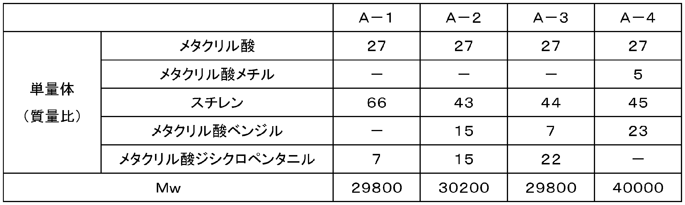
- Binder polymer (A-2) and (A-3) As the polymerizable monomer, methacrylic acid, styrene, benzyl methacrylate, and dicyclopentanyl methacrylate were used in the mass ratio shown in Table 1 in the same manner as in obtaining the solution of the binder polymer (A-1). To obtain a solution of binder polymers (A-2) and (A-3).
- Binder polymer (A-4) As the polymerizable monomer, methacrylic acid, methyl methacrylate, styrene, and benzyl methacrylate were used in the mass ratio shown in Table 1, except that the binder polymer (A-1) solution was obtained in the same manner as described above. A solution of polymer (A-4) was obtained.
- Table 1 shows the mass ratio (%) and Mw of the polymerizable monomers for the binder polymers (A-1) to (A-4).
- Examples 1 to 3 and Comparative Example 1 ⁇ Preparation of photosensitive resin composition>
- the binder polymers (A-1) to (A-4) are mixed in the blending amounts (parts by mass) shown in Table 2 below, (B) a photopolymerizable compound, (C) a photopolymerization initiator, and (D) a sensitizer. , And other components, and a solvent were mixed to prepare photosensitive resin compositions of Examples and Comparative Examples, respectively.
- the compounding amount of the binder polymer shown in Table 2 is the mass (solid content) of the nonvolatile content.
- the solution of the photosensitive resin composition was uniformly applied on a 16 ⁇ m thick polyethylene terephthalate film (trade name “FB40” manufactured by Toray Industries, Inc.) and dried for 10 minutes by a hot air convection dryer at 90° C., It was protected with a polyethylene film (Tama Poly Co., Ltd., trade name "NF-15A") to obtain a photosensitive resin composition laminate (photosensitive element).
- the film thickness of the photosensitive layer after drying was 5 ⁇ m.
- a copper sputtered wafer (trade name “AMT”) was washed with water, pickled and washed with water, and then dried with an air stream. Then, the copper sputtered wafer was heated to 80° C., and the photosensitive element was laminated on the copper surface of the copper sputtered wafer. The lamination was carried out by peeling off the protective layer so that the photosensitive layer of the photosensitive element was in contact with the copper surface of the copper sputtered wafer and using a heat roll at 110° C., a pressure of 0.4 MPa and a pressure of 1.0 m/min. At a roll speed of. Thus, a laminated body was obtained in which the copper sputtered wafer, the photosensitive layer, and the support were laminated in this order. The obtained laminated body was used as a test piece for the following test.
- the support is peeled off to expose the photosensitive layer, and a 1% by mass sodium carbonate aqueous solution at 30° C. is sprayed for a time twice as long as the shortest development time (the shortest time for removing the unexposed portion) to unexpose.
- the part was removed (development process).
- the energy amount (mJ/cm 2 ) at which the step number of the step tablets of the photo-cured film formed on the substrate was 10.0 steps was obtained, and the photosensitivity of the photosensitive resin composition was evaluated.
- Table 2 The results are shown in Table 2. The smaller this value is, the higher the sensitivity is.
- a glass chrome type photo tool (resolution negative: line width/space width x/x (x: 1 to 18, unit: ⁇ m ), the adhesive negative: a line width/space width x/x (x: 1 to 18, unit: ⁇ m) wiring pattern) is used to develop a Hitachi 41-step step tablet. Exposure was performed with an energy amount such that the number of remaining step steps after the afterimage was 10.0. After the exposure, the film was developed as in the photosensitivity test.
Landscapes
- Chemical & Material Sciences (AREA)
- Physics & Mathematics (AREA)
- Engineering & Computer Science (AREA)
- General Physics & Mathematics (AREA)
- Chemical Kinetics & Catalysis (AREA)
- Health & Medical Sciences (AREA)
- Microelectronics & Electronic Packaging (AREA)
- Manufacturing & Machinery (AREA)
- Medicinal Chemistry (AREA)
- Polymers & Plastics (AREA)
- Organic Chemistry (AREA)
- Spectroscopy & Molecular Physics (AREA)
- Materials For Photolithography (AREA)
- Manufacturing Of Printed Circuit Boards (AREA)
- Exposure And Positioning Against Photoresist Photosensitive Materials (AREA)
- Manufacturing Of Printed Wiring (AREA)
Abstract
Description
本実施形態の感光性樹脂組成物は、(A)成分:バインダーポリマーと、(B)成分:光重合性化合物と、(C)成分:光重合開始剤と、を含有する。バインターポリマーは、ジシクロペンタニル基を有する(メタ)アクリレート化合物に由来する構造単位を含む。上記感光性樹脂組成物は、必要に応じて、(D)成分:340nm~430nmに吸収極大を有する増感色素、水素供与体又はその他の成分を更に含有してもよい。以下、本実施形態の感光性樹脂組成物で用いられる各成分についてより詳細に説明する。
本実施形態の感光性樹脂組成物によれば、上記(A)~(C)成分を含有することにより、解像性及び密着性に優れ、微細なレジストパターンを形成することが可能である。特に、ジシクロペンタニル基を有する(メタ)アクリレート化合物に由来する構造単位を含むバインターポリマーを用いることにより、解像性及び密着性をより高めることができたものと推察する。

酸価=0.1×Vf×56.1/(Wp×I/100)
式中、VfはKOH水溶液の滴定量(mL)を示し、Wpは測定したバインダーポリマーを含有する溶液の質量(g)を示し、Iは測定したバインダーポリマーを含有する溶液中の不揮発分の割合(質量%)を示す。
なお、バインダーポリマーを合成溶媒、希釈溶媒等の揮発分と混合した状態で配合する場合は、精秤前に予め、揮発分の沸点よりも10℃以上高い温度で1~4時間加熱し、揮発分を除去してから酸価を測定することもできる。
(B)成分としては、エチレン性不飽和結合の少なくとも1つを有し、光重合可能な化合物であれば特に限定されない。(B)成分としては、アルカリ現像性、解像性、及び硬化後の剥離特性を向上させる観点から、ビスフェノール型(メタ)アクリレートの少なくとも1種を含むことが好ましく、ビスフェノール型(メタ)アクリレートの中でもビスフェノールA型(メタ)アクリレートを含むことがより好ましい。ビスフェノールA型(メタ)アクリレートとしては、例えば、2,2-ビス(4-((メタ)アクリロキシポリエトキシ)フェニル)プロパン、2,2-ビス(4-((メタ)アクリロキシポリプロポキシ)フェニル)プロパン、2,2-ビス(4-((メタ)アクリロキシポリブトキシ)フェニル)プロパン、及び2,2-ビス(4-((メタ)アクリロキシポリエトキシポリプロポキシ)フェニル)プロパンが挙げられる。中でも、解像性、及び剥離特性を更に向上させる観点から2,2-ビス(4-((メタ)アクリロキシポリエトキシ)フェニル)プロパンが好ましい。
(C)成分としては、特に制限はないが、感度及び解像性をバランスよく向上する点で、ヘキサアリールビイミダゾール誘導体、又は、アクリジニル基を1つ以上有するアクリジン化合物を用いてよい。特に、390nm~420nmの活性光線を用いて感光層の露光を行う場合には、感度及び密着性の観点から、(C)成分は、アクリジニル基を1つ以上有するアクリジン化合物を含んでよい。
本実施形態の感光性樹脂組成物は、増感剤を更に含有してよい。これにより、感光性樹脂組成物の光感度が更に良好となる。増感剤としては、例えば、ジアルキルアミノベンゾフェノン化合物、ピラゾリン化合物、アントラセン化合物、クマリン化合物、キサントン化合物、オキサゾール化合物、ベンゾオキサゾール化合物、チアゾール化合物、ベンゾチアゾール化合物、トリアゾール化合物、スチルベン化合物、トリアジン化合物、チオフェン化合物、ナフタルイミド化合物、及びトリアリールアミン化合物が挙げられる。これらは1種単独で又は2種以上を組み合わせて使用される。(D)成分は、340~430nmに吸収極大を有する増感色素を含んでよい。340~430nmの活性光線を用いて感光層の露光を行う場合には、感度及び密着性の観点から、ピラゾリン化合物、アントラセン化合物、クマリン化合物及びトリアリールアミン化合物からなる群より選ばれる少なくとも1種を含んでよく、中でもピラゾリン化合物、アントラセン化合物及びトリアリールアミン化合物からなる群より選ばれる少なくとも1種を含んでよい。
感光性樹脂組成物は、水素供与体を更に含有してよい。これにより、感光性樹脂組成物の感度が更に良好となる。水素供与体としては、例えば、ビス[4-(ジメチルアミノ)フェニル]メタン、ビス[4-(ジエチルアミノ)フェニル]メタン、N-フェニルグリシン、及びロイコクリスタルバイオレットが挙げられる。これらは1種単独で又は2種以上を組み合わせて使用される。
感光性樹脂組成物は、必要に応じて、その他の成分を更に含有することができる。その他の成分としては、例えば、分子内に少なくとも1つのカチオン重合可能な環状エーテル基を有する光重合性化合物(オキセタン化合物等)、カチオン重合開始剤、染料(マラカイトグリーン等)、トリブロモフェニルスルホン、光発色剤、熱発色防止剤、可塑剤(p-トルエンスルホンアミド等)、重合禁止剤(tert-ブチルカテコール等)、シランカップリング剤、顔料、充填剤、消泡剤、難燃剤、安定剤、密着性付与剤(ベンゾトリアゾール等)、レベリング剤、剥離促進剤、酸化防止剤、香料、イメージング剤、熱架橋剤等が挙げられる。これらは1種単独で又は2種以上を組み合わせて使用される。その他の成分の含有量は、それぞれ0.01~20質量%程度であってもよい。
本実施形態の感光性エレメントは、支持体と、該支持体上に形成された上記感光性樹脂組成物を含む感光層と、を備える。本実施形態の感光性エレメントを用いる場合には、感光層を基板上にラミネートした後、支持体を剥離することなく露光してもよい。
支持体しては、ポリエチレンテレフタレート(PET)等のポリエステル、ポリプロピレン、ポリエチレン等のポリオレフィンなどの耐熱性及び耐溶剤性を有する重合体フィルム(支持フィルム)を用いることができる。中でも、入手し易く、かつ、製造工程におけるハンドリング性(特に、耐熱性、熱収縮率、破断強度)に優れる点で、PETフィルムであってもよい。
感光性エレメントは、必要に応じて保護層を更に備えてもよい。保護層としては、感光層と支持体との間の接着力よりも、感光層と保護層との間の接着力が小さくなるようなフィルムを用いてもよく、また、低フィッシュアイのフィルムを用いてもよい。具体的には、例えば、上述する支持体として用いることができるものが挙げられる。感光層からの剥離性の見地から、ポリエチレンフィルムであってもよい。保護層の厚さは、用途により異なるが、1~100μm程度であってよい。
感光性エレメントは、例えば、以下のようにして製造することができる。上述する塗布液を調製することと、塗布液を支持体上に塗布して塗布層を形成することと、塗布層を乾燥して感光層を形成することと、を含む製造方法で製造することができる。塗布液の支持体上への塗布は、例えば、ロールコート、コンマコート、グラビアコート、エアーナイフコート、ダイコート、バーコート等の公知の方法により行うことができる。
本実施形態のレジストパターンの形成方法は、上記感光性樹脂組成物を含む感光層、又は上記感光性エレメントの感光層を基板上に積層する感光層形成工程と、感光層の所定部分に活性光線を照射して光硬化部を形成する露光工程と、感光層の所定部分以外の領域を基板上から除去する現像工程と、を有する。レジストパターンの形成方法は、必要に応じてその他の工程を有してもよい。なお、レジストパターンとは、感光性樹脂組成物の、光硬化物パターンともいえ、レリーフパターンともいえる。また、レジストパターンの形成方法は、レジストパターン付き基板の製造方法ともいえる。
基板上に感光層を形成する方法としては、例えば、感光性樹脂組成物を塗布及び乾燥してもよく、又は、感光性エレメントから保護層を除去した後、感光性エレメントの感光層を加熱しながら上記基板に圧着してもよい。感光性エレメントを用いた場合、基板と感光層と支持体とからなり、これらが順に積層された積層体が得られる。基板としては特に制限されないが、通常、絶縁層と絶縁層上に形成された導体層とを備えた回路形成用基板、又は合金基材等のダイパッド(リードフレーム用基材)が用いられる。
露光工程においては、基板上に形成された感光層の少なくとも一部に活性光線を照射することで、活性光線が照射された部分が光硬化して、潜像が形成される。この際、感光性樹脂層上に存在する支持体が活性光線に対して透過性である場合には、支持体を通して活性光線を照射することができるが、支持体が遮光性の場合には、支持体を除去した後に感光性樹脂層に活性光線を照射する。
現像工程においては、感光層の光硬化部以外の少なくとも一部が基板上から除去されることで、レジストパターンが基板上に形成される。感光層上に支持体が存在している場合には、支持体を除去してから、上記光硬化部以外の領域(未露光部分ともいえる)の除去(現像)を行う。現像方法には、ウェット現像とドライ現像とがあるが、ウェット現像が広く用いられている。
本実施形態のプリント配線板の製造方法は、上記レジストパターンの形成方法によりレジストパターンが形成された基板をエッチング処理又はめっき処理して、導体パターンを形成する工程を含む。プリント配線板の製造方法は、必要に応じて、レジストパターン除去工程等のその他の工程を含んでもよい。
重合性単量体(モノマー)であるメタクリル酸95g、スチレン232g、ジシクロペンタニルメタクリレート26g、及びアゾビスイソブチロニトリル4gを混合して、溶液aを調製した。また、1-メトキシ2-プロパノール11g及びトルエン6gの混合液(質量比3:2)にアゾビスイソブチロニトリル0.4gを混合して、溶液bを調製した。
カラム:Gelpack GL-R440、Gelpack GL-R450及びGelpack GL-R400M(以上、日立化成(株))を連結
溶離液:テトラヒドロフラン
測定温度:40℃
流量:2.05mL/分
検出器:日立 L-2490型RI((株)日立製作所)
重合性単量体として、表1に示す質量比でメタクリル酸、スチレン、メタクリル酸ベンジル、及びジシクロペンタニルメタクリレートを用いた以外は、バインダーポリマー(A-1)の溶液を得るのと同様にしてバインダーポリマー(A-2)及び(A-3)の溶液を得た。
重合性単量体として、表1に示す質量比でメタクリル酸、メタクリル酸メチル、スチレン、及びメタクリル酸ベンジルを用いた以外は、バインダーポリマー(A-1)の溶液を得るのと同様にしてバインダーポリマー(A-4)の溶液を得た。
<感光性樹脂組成物の調製>
下記表2に示す配合量(質量部)で、バインダーポリマー(A-1)~(A-4)を、(B)光重合性化合物、(C)光重合開始剤、(D)増感剤、その他の成分、及び溶剤と混合することにより、実施例及び比較例の感光性樹脂組成物をそれぞれ調製した。なお、表2に示すバインダーポリマーの配合量は、不揮発分の質量(固形分量)である。
FA-024M:(PO)(EO)(PO)変性ポリエチレングリコールジメタクリレート(EO平均6mol及びPO平均12mol変性)(日立化成(株)製、商品名)
FA-321M:2,2-ビス(4-(メタクリロキシペンタエトキシ)フェニル)プロパン(日立化成(株)製、商品名)
BPE-200:エトキシ化ビスフェノールAジメタクリレート(EO平均4mol変性)(新中村化学工業(株)製、商品名)
((C)光重合開始剤)
B-CIM:2,2’-ビス(2-クロロフェニル)-4,4’,5,5’-テトラフェニル-1,2-ビイミダゾール(保土ヶ谷化学工業(株)製、商品名)
((D)増感剤)
PZ―501D:1-フェニル-3-(4―メトキシスチリル)-5-(4-メトキシフェニル)ピラゾリン((株)日本化学工業所製、商品名)
SF-808H:ベンゾトリアゾール誘導体(サンワ化成(株)製、商品名)
(その他の成分)
LCV:ロイコクリスタルバイオレット(山田化学(株)製、商品名)
MKG:マラカイトグリーン(大阪有機化学工業(株)製、商品名)
TBC:tert-ブチルカテコール(富士フイルム和光純薬(株)製、商品名)
KBM-803:3-メルカプトプロピルトリメトキシシラン(信越化学工業(株)製、商品名)
感光性樹脂組成物の溶液を、16μm厚のポリエチレンテレフタレートフィルム(東レ(株)製、商品名「FB40」)上に均一に塗布し、90℃の熱風対流式乾燥機で10分間乾燥した後、ポリエチレンフィルム(タマポリ(株)製、商品名「NF-15A」)で保護し感光性樹脂組成物積層体(感光性エレメント)を得た。感光層の乾燥後の膜厚は、5μmであった。
銅スパッタウエハ(商品名「AMT」)を水洗、酸洗及び水洗後、空気流で乾燥した。その後、銅スパッタウエハを80℃に加温し、感光性エレメントを銅スパッタウエハの銅表面にラミネート(積層)した。ラミネートは、保護層を剥離しながら、感光性エレメントの感光層が銅スパッタウエハの銅表面に接するようにして、110℃のヒートロールを用いて、0.4MPaの圧着圧力、1.0m/分のロール速度で行った。こうして、銅スパッタウエハと感光層と支持体とがこの順で積層された積層体を得た。得られた積層体は以下に示す試験の試験片として用いた。
試験片の支持体の上に、ネガマスクとして濃度領域0.00~2.00、濃度ステップ0.05、タブレットの大きさが20mm×187mm、各ステップの大きさが3mm×12mmである41段ステップタブレットを有するフォトツール載置した。次いで、波長355nmの半導体レーザを光源とする投影露光装置((株)サーマプレシジョン製、商品名「ASS Mk1.3 Ck-Lens」)を用いて、所定のエネルギー量で感光層を露光した。
試験片の支持体上に、解像性ネガ及び密着性評価用ネガとしてガラスクロムタイプのフォトツール(解像性ネガ:ライン幅/スペース幅がx/x(x:1~18、単位:μm)の配線パターンを有するもの、密着性ネガ:ライン幅/スペース幅がx/x(x:1~18、単位:μm)の配線パターンを有するもの)を使用し、日立41段ステップタブレットの現像後の残像後の残存ステップ段数が10.0となるエネルギー量で露光を行った。露光後、上記光感度測定試験と同様に、現像処理した。

Claims (7)
- バインターポリマーと、光重合性化合物と、光重合開始剤と、を含有する感光性樹脂組成物であって、
前記バインターポリマーが、ジシクロペンタニル基を有する(メタ)アクリレート化合物に由来する構造単位を含む、感光性樹脂組成物。 - 前記ジシクロペンタニル基を有する(メタ)アクリレート化合物に由来する構造単位の含有量が、前記バインターポリマーを構成する重合性単量体に由来する構造単位の全質量を基準として、1~50質量%である、請求項1に記載の感光性樹脂組成物。
- 340~430nmに吸収極大を有する増感色素を更に含有する、請求項1又は2に記載の感光性樹脂組成物。
- 支持体と、該支持体上に形成された請求項1~3のいずれか一項に記載の感光性樹脂組成物を含む感光層と、を備える感光性エレメント。
- 請求項1~3のいずれか一項に記載の感光性樹脂組成物を含む感光層、又は請求項4に記載の感光性エレメントの感光層を基板上に積層する感光層形成工程と、
前記感光層の所定部分に活性光線を照射して光硬化部を形成する露光工程と、
前記感光層の前記所定部分以外の領域を前記基板上から除去する現像工程と、を有するレジストパターンの形成方法。 - 前記活性光線の波長が340nm~430nmの範囲内である、請求項5に記載のレジストパターンの形成方法。
- 請求項5又は請求項6に記載のレジストパターンの形成方法によりレジストパターンが形成された基板をエッチング処理又はめっき処理して、導体パターンを形成する工程を含む、プリント配線板の製造方法。
Priority Applications (5)
| Application Number | Priority Date | Filing Date | Title |
|---|---|---|---|
| JP2020571219A JP7793291B2 (ja) | 2019-02-05 | 2020-02-04 | 感光性樹脂組成物、感光性エレメント、レジストパターンの形成方法及びプリント配線板の製造方法 |
| KR1020217026730A KR20210124281A (ko) | 2019-02-05 | 2020-02-04 | 감광성 수지 조성물, 감광성 엘리먼트, 레지스트 패턴의 형성 방법 및 프린트 배선판의 제조 방법 |
| CN202080012460.XA CN113412289B (zh) | 2019-02-05 | 2020-02-04 | 感光性树脂组合物、感光性元件、抗蚀剂图案的形成方法及印刷线路板的制造方法 |
| CN202410290771.2A CN118131567A (zh) | 2019-02-05 | 2020-02-04 | 感光性树脂组合物、感光性元件、抗蚀剂图案的形成方法及印刷线路板的制造方法 |
| JP2024073674A JP2024096278A (ja) | 2019-02-05 | 2024-04-30 | 感光性樹脂組成物、感光性エレメント、レジストパターンの形成方法及びプリント配線板の製造方法 |
Applications Claiming Priority (2)
| Application Number | Priority Date | Filing Date | Title |
|---|---|---|---|
| JP2019018925 | 2019-02-05 | ||
| JP2019-018925 | 2019-02-05 |
Publications (1)
| Publication Number | Publication Date |
|---|---|
| WO2020162464A1 true WO2020162464A1 (ja) | 2020-08-13 |
Family
ID=71948019
Family Applications (1)
| Application Number | Title | Priority Date | Filing Date |
|---|---|---|---|
| PCT/JP2020/004182 Ceased WO2020162464A1 (ja) | 2019-02-05 | 2020-02-04 | 感光性樹脂組成物、感光性エレメント、レジストパターンの形成方法及びプリント配線板の製造方法 |
Country Status (5)
| Country | Link |
|---|---|
| JP (2) | JP7793291B2 (ja) |
| KR (1) | KR20210124281A (ja) |
| CN (2) | CN118131567A (ja) |
| TW (1) | TWI882983B (ja) |
| WO (1) | WO2020162464A1 (ja) |
Cited By (5)
| Publication number | Priority date | Publication date | Assignee | Title |
|---|---|---|---|---|
| WO2022030053A1 (ja) * | 2020-08-07 | 2022-02-10 | 昭和電工マテリアルズ株式会社 | 感光性樹脂組成物、感光性エレメント、レジストパターンの形成方法、及びプリント配線板の製造方法 |
| JPWO2022191125A1 (ja) * | 2021-03-09 | 2022-09-15 | ||
| WO2023233543A1 (ja) * | 2022-05-31 | 2023-12-07 | 株式会社レゾナック | パターン形成方法及びパターン形成構造 |
| WO2025005146A1 (ja) * | 2023-06-27 | 2025-01-02 | 旭化成株式会社 | 感光性樹脂組成物、感光性樹脂積層体、及びレジストパターンの形成方法等 |
| EP4607279A4 (en) * | 2022-12-23 | 2025-08-27 | Resonac Corp | PHOTOSENSITIVE RESIN COMPOSITION, PHOTOSENSITIVE ELEMENT, METHOD FOR FORMING RESIST PATTERN, AND METHOD FOR PRODUCING PRINTED CIRCUIT BOARD |
Families Citing this family (3)
| Publication number | Priority date | Publication date | Assignee | Title |
|---|---|---|---|---|
| WO2022030052A1 (ja) * | 2020-08-07 | 2022-02-10 | 昭和電工マテリアルズ株式会社 | 感光性樹脂組成物、感光性エレメント、レジストパターンの形成方法、及びプリント配線板の製造方法 |
| WO2022102101A1 (ja) * | 2020-11-13 | 2022-05-19 | 昭和電工マテリアルズ株式会社 | 感光性エレメント、硬化物の製造方法、硬化物パターンの製造方法、及び、配線板の製造方法 |
| WO2022113161A1 (ja) * | 2020-11-24 | 2022-06-02 | 昭和電工マテリアルズ株式会社 | 感光性樹脂組成物、感光性エレメント、レジストパターンの形成方法及びプリント配線板の製造方法 |
Citations (3)
| Publication number | Priority date | Publication date | Assignee | Title |
|---|---|---|---|---|
| JP2001290265A (ja) * | 2000-04-05 | 2001-10-19 | Jsr Corp | 感放射線性樹脂組成物及びこれを用いたフォトリソグラフィ |
| JP2018151489A (ja) * | 2017-03-10 | 2018-09-27 | 東京応化工業株式会社 | 感光性組成物、ドライフィルム、及びパターン化された硬化膜を形成する方法 |
| JP2018204011A (ja) * | 2017-06-08 | 2018-12-27 | Jsr株式会社 | 組成物、硬化膜の製造方法及び電子部品 |
Family Cites Families (13)
| Publication number | Priority date | Publication date | Assignee | Title |
|---|---|---|---|---|
| JP3688949B2 (ja) * | 1999-09-24 | 2005-08-31 | 昭和高分子株式会社 | 感光性樹脂 |
| JP4172209B2 (ja) * | 2002-05-31 | 2008-10-29 | 日立化成工業株式会社 | 感光性樹脂組成物、これを用いた感光性エレメント、レジストパターンの製造方法及びプリント配線板の製造方法 |
| JP2009003366A (ja) * | 2007-06-25 | 2009-01-08 | Jsr Corp | マイクロレンズ形成に用いられる感放射線性樹脂組成物 |
| TWI459131B (zh) * | 2008-05-20 | 2014-11-01 | Toyo Ink Mfg Co | 彩色濾光片用感光性著色組成物及彩色濾光片 |
| JP2010085929A (ja) * | 2008-10-02 | 2010-04-15 | Jsr Corp | 感放射線性樹脂組成物および液晶表示素子用スペーサーとその製造法 |
| CN102070744B (zh) * | 2009-11-19 | 2014-12-17 | Dnp精细化工股份有限公司 | 抗蚀剂墨液用粘结剂树脂和使用其的抗蚀剂墨液 |
| KR20130047656A (ko) * | 2011-10-31 | 2013-05-08 | 히타치가세이가부시끼가이샤 | 감광성 수지 조성물, 감광성 엘리먼트, 레지스트 패턴의 형성 방법 및 인쇄 배선판의 제조 방법 |
| JP6229256B2 (ja) | 2011-10-31 | 2017-11-15 | 日立化成株式会社 | 感光性エレメント、レジストパターンの形成方法及びプリント配線板の製造方法 |
| JP5935337B2 (ja) | 2012-01-16 | 2016-06-15 | 日立化成株式会社 | 液状光硬化性樹脂組成物、光学部材、画像表示用装置及びその製造方法 |
| JP2013195712A (ja) | 2012-03-19 | 2013-09-30 | Hitachi Chemical Co Ltd | 感光性樹脂組成物、感光性エレメント、レジストパターンの形成方法及びプリント配線板の製造方法 |
| JP2015072336A (ja) * | 2013-10-02 | 2015-04-16 | Jnc株式会社 | 感光性組成物及びそれを用いた表示素子 |
| JPWO2016104585A1 (ja) | 2014-12-25 | 2017-10-05 | 日立化成株式会社 | 感光性樹脂組成物、並びにこれを用いた感光性エレメント、レジストパターンの形成方法、及びプリント配線板の製造方法 |
| TWI859361B (zh) * | 2019-11-21 | 2024-10-21 | 日商富士軟片股份有限公司 | 圖案形成方法、光硬化性樹脂組成物、積層體的製造方法及電子元件的製造方法 |
-
2020
- 2020-02-04 TW TW109103400A patent/TWI882983B/zh active
- 2020-02-04 JP JP2020571219A patent/JP7793291B2/ja active Active
- 2020-02-04 KR KR1020217026730A patent/KR20210124281A/ko not_active Ceased
- 2020-02-04 WO PCT/JP2020/004182 patent/WO2020162464A1/ja not_active Ceased
- 2020-02-04 CN CN202410290771.2A patent/CN118131567A/zh active Pending
- 2020-02-04 CN CN202080012460.XA patent/CN113412289B/zh active Active
-
2024
- 2024-04-30 JP JP2024073674A patent/JP2024096278A/ja not_active Withdrawn
Patent Citations (3)
| Publication number | Priority date | Publication date | Assignee | Title |
|---|---|---|---|---|
| JP2001290265A (ja) * | 2000-04-05 | 2001-10-19 | Jsr Corp | 感放射線性樹脂組成物及びこれを用いたフォトリソグラフィ |
| JP2018151489A (ja) * | 2017-03-10 | 2018-09-27 | 東京応化工業株式会社 | 感光性組成物、ドライフィルム、及びパターン化された硬化膜を形成する方法 |
| JP2018204011A (ja) * | 2017-06-08 | 2018-12-27 | Jsr株式会社 | 組成物、硬化膜の製造方法及び電子部品 |
Cited By (8)
| Publication number | Priority date | Publication date | Assignee | Title |
|---|---|---|---|---|
| WO2022030053A1 (ja) * | 2020-08-07 | 2022-02-10 | 昭和電工マテリアルズ株式会社 | 感光性樹脂組成物、感光性エレメント、レジストパターンの形成方法、及びプリント配線板の製造方法 |
| JPWO2022191125A1 (ja) * | 2021-03-09 | 2022-09-15 | ||
| WO2022191125A1 (ja) * | 2021-03-09 | 2022-09-15 | 昭和電工マテリアルズ株式会社 | 感光性フィルム、感光性エレメント、及び、積層体の製造方法 |
| WO2023233543A1 (ja) * | 2022-05-31 | 2023-12-07 | 株式会社レゾナック | パターン形成方法及びパターン形成構造 |
| JPWO2023233543A1 (ja) * | 2022-05-31 | 2023-12-07 | ||
| JP7666741B2 (ja) | 2022-05-31 | 2025-04-22 | 株式会社レゾナック | パターン形成方法及びパターン形成構造 |
| EP4607279A4 (en) * | 2022-12-23 | 2025-08-27 | Resonac Corp | PHOTOSENSITIVE RESIN COMPOSITION, PHOTOSENSITIVE ELEMENT, METHOD FOR FORMING RESIST PATTERN, AND METHOD FOR PRODUCING PRINTED CIRCUIT BOARD |
| WO2025005146A1 (ja) * | 2023-06-27 | 2025-01-02 | 旭化成株式会社 | 感光性樹脂組成物、感光性樹脂積層体、及びレジストパターンの形成方法等 |
Also Published As
| Publication number | Publication date |
|---|---|
| JP2024096278A (ja) | 2024-07-12 |
| JPWO2020162464A1 (ja) | 2021-12-02 |
| JP7793291B2 (ja) | 2026-01-05 |
| TWI882983B (zh) | 2025-05-11 |
| CN118131567A (zh) | 2024-06-04 |
| KR20210124281A (ko) | 2021-10-14 |
| CN113412289A (zh) | 2021-09-17 |
| CN113412289B (zh) | 2024-04-05 |
| TW202040272A (zh) | 2020-11-01 |
Similar Documents
| Publication | Publication Date | Title |
|---|---|---|
| JP7793291B2 (ja) | 感光性樹脂組成物、感光性エレメント、レジストパターンの形成方法及びプリント配線板の製造方法 | |
| JP7593405B2 (ja) | 感光性樹脂組成物、感光性エレメント、レジストパターンの形成方法、及びプリント配線板の製造方法 | |
| JP5626428B2 (ja) | 感光性樹脂組成物、並びにこれを用いた感光性エレメント、レジストパターンの形成方法及びプリント配線板の製造方法 | |
| JP6782417B2 (ja) | 感光性樹脂組成物、感光性エレメント、レジストパターンの形成方法及びプリント配線板の製造方法 | |
| WO2015012272A1 (ja) | 投影露光用感光性樹脂組成物、感光性エレメント、レジストパターンの形成方法、プリント配線板の製造方法及びリードフレームの製造方法 | |
| JP6828546B2 (ja) | 感光性樹脂組成物、感光性エレメント、レジストパターンの形成方法及びプリント配線板の製造方法 | |
| JP7609119B2 (ja) | 感光性樹脂組成物、感光性エレメント、レジストパターンの形成方法及びプリント配線板の製造方法 | |
| JP2017040710A (ja) | 感光性樹脂組成物、感光性エレメント、レジストパターンの形成方法及びプリント配線板の製造方法 | |
| JP2017191171A (ja) | 感光性樹脂組成物、感光性エレメント、レジストパターンの形成方法及びプリント配線板の製造方法 | |
| JP7670060B2 (ja) | 感光性樹脂組成物、感光性エレメント、レジストパターンの形成方法、及びプリント配線板の製造方法 | |
| JP5853588B2 (ja) | 感光性樹脂組成物、感光性エレメント、レジストパターンの形成方法及びプリント配線板の製造方法 | |
| JP2018138962A (ja) | レーザー直描露光用感光性樹脂組成物、感光性エレメント、レジストパターンの形成方法及びプリント配線板の製造方法 | |
| KR20260056311A (ko) | 감광성 수지 조성물, 감광성 엘리먼트, 레지스트 패턴의 형성 방법 및 프린트 배선판의 제조 방법 | |
| WO2024009870A1 (ja) | 感光性樹脂組成物、感光性エレメント、レジストパターンの形成方法、及び、半導体パッケージ基板又はプリント配線板の製造方法 | |
| CN121978867A (en) | Photosensitive resin composition, photosensitive element, method for forming resist pattern, and method for manufacturing printed wiring board | |
| WO2018100640A1 (ja) | 感光性樹脂組成物、感光性エレメント、レジストパターン付き基板の製造方法、及び、プリント配線板の製造方法 | |
| WO2024135574A1 (ja) | 感光性樹脂組成物、感光性エレメント、レジストパターンの形成方法、及びプリント配線板の製造方法 | |
| WO2024134889A1 (ja) | 感光性樹脂組成物、感光性エレメント、レジストパターンの形成方法、及びプリント配線板の製造方法 | |
| WO2025094282A1 (ja) | 感光性エレメント、レジストパターンの形成方法、及びプリント配線板の製造方法 |
Legal Events
| Date | Code | Title | Description |
|---|---|---|---|
| 121 | Ep: the epo has been informed by wipo that ep was designated in this application |
Ref document number: 20752019 Country of ref document: EP Kind code of ref document: A1 |
|
| ENP | Entry into the national phase |
Ref document number: 2020571219 Country of ref document: JP Kind code of ref document: A |
|
| NENP | Non-entry into the national phase |
Ref country code: DE |
|
| ENP | Entry into the national phase |
Ref document number: 20217026730 Country of ref document: KR Kind code of ref document: A |
|
| 32PN | Ep: public notification in the ep bulletin as address of the adressee cannot be established |
Free format text: NOTING OF LOSS OF RIGHTS PURSUANT TO RULE 112(1) EPC (EPO FORM 1205A DATED 05.11.2021) |
|
| 122 | Ep: pct application non-entry in european phase |
Ref document number: 20752019 Country of ref document: EP Kind code of ref document: A1 |
|
| WWR | Wipo information: refused in national office |
Ref document number: 1020217026730 Country of ref document: KR |
|
| WWC | Wipo information: continuation of processing after refusal or withdrawal |
Ref document number: 1020217026730 Country of ref document: KR |