WO2020162451A1 - 光機能素子およびレーザ素子 - Google Patents
光機能素子およびレーザ素子 Download PDFInfo
- Publication number
- WO2020162451A1 WO2020162451A1 PCT/JP2020/004120 JP2020004120W WO2020162451A1 WO 2020162451 A1 WO2020162451 A1 WO 2020162451A1 JP 2020004120 W JP2020004120 W JP 2020004120W WO 2020162451 A1 WO2020162451 A1 WO 2020162451A1
- Authority
- WO
- WIPO (PCT)
- Prior art keywords
- optical
- input
- optical coupler
- width
- output ports
- Prior art date
- Legal status (The legal status is an assumption and is not a legal conclusion. Google has not performed a legal analysis and makes no representation as to the accuracy of the status listed.)
- Ceased
Links
Images


Classifications
-
- H—ELECTRICITY
- H01—ELECTRIC ELEMENTS
- H01S—DEVICES USING THE PROCESS OF LIGHT AMPLIFICATION BY STIMULATED EMISSION OF RADIATION [LASER] TO AMPLIFY OR GENERATE LIGHT; DEVICES USING STIMULATED EMISSION OF ELECTROMAGNETIC RADIATION IN WAVE RANGES OTHER THAN OPTICAL
- H01S5/00—Semiconductor lasers
- H01S5/10—Construction or shape of the optical resonator, e.g. extended or external cavity, coupled cavities, bent-guide, varying width, thickness or composition of the active region
- H01S5/1003—Waveguide having a modified shape along the axis, e.g. branched, curved, tapered, voids
- H01S5/101—Curved waveguide
-
- H—ELECTRICITY
- H01—ELECTRIC ELEMENTS
- H01S—DEVICES USING THE PROCESS OF LIGHT AMPLIFICATION BY STIMULATED EMISSION OF RADIATION [LASER] TO AMPLIFY OR GENERATE LIGHT; DEVICES USING STIMULATED EMISSION OF ELECTROMAGNETIC RADIATION IN WAVE RANGES OTHER THAN OPTICAL
- H01S5/00—Semiconductor lasers
- H01S5/10—Construction or shape of the optical resonator, e.g. extended or external cavity, coupled cavities, bent-guide, varying width, thickness or composition of the active region
- H01S5/14—External cavity lasers
- H01S5/141—External cavity lasers using a wavelength selective device, e.g. a grating or etalon
- H01S5/142—External cavity lasers using a wavelength selective device, e.g. a grating or etalon which comprises an additional resonator
-
- G—PHYSICS
- G02—OPTICS
- G02B—OPTICAL ELEMENTS, SYSTEMS OR APPARATUS
- G02B6/00—Light guides; Structural details of arrangements comprising light guides and other optical elements, e.g. couplings
- G02B6/10—Light guides; Structural details of arrangements comprising light guides and other optical elements, e.g. couplings of the optical waveguide type
- G02B6/12—Light guides; Structural details of arrangements comprising light guides and other optical elements, e.g. couplings of the optical waveguide type of the integrated circuit kind
- G02B6/12007—Light guides; Structural details of arrangements comprising light guides and other optical elements, e.g. couplings of the optical waveguide type of the integrated circuit kind forming wavelength selective elements, e.g. multiplexer, demultiplexer
-
- G—PHYSICS
- G02—OPTICS
- G02B—OPTICAL ELEMENTS, SYSTEMS OR APPARATUS
- G02B6/00—Light guides; Structural details of arrangements comprising light guides and other optical elements, e.g. couplings
- G02B6/24—Coupling light guides
- G02B6/26—Optical coupling means
- G02B6/28—Optical coupling means having data bus means, i.e. plural waveguides interconnected and providing an inherently bidirectional system by mixing and splitting signals
- G02B6/293—Optical coupling means having data bus means, i.e. plural waveguides interconnected and providing an inherently bidirectional system by mixing and splitting signals with wavelength selective means
- G02B6/29331—Optical coupling means having data bus means, i.e. plural waveguides interconnected and providing an inherently bidirectional system by mixing and splitting signals with wavelength selective means operating by evanescent wave coupling
- G02B6/29335—Evanescent coupling to a resonator cavity, i.e. between a waveguide mode and a resonant mode of the cavity
- G02B6/29338—Loop resonators
-
- G—PHYSICS
- G02—OPTICS
- G02B—OPTICAL ELEMENTS, SYSTEMS OR APPARATUS
- G02B6/00—Light guides; Structural details of arrangements comprising light guides and other optical elements, e.g. couplings
- G02B6/24—Coupling light guides
- G02B6/26—Optical coupling means
- G02B6/28—Optical coupling means having data bus means, i.e. plural waveguides interconnected and providing an inherently bidirectional system by mixing and splitting signals
- G02B6/293—Optical coupling means having data bus means, i.e. plural waveguides interconnected and providing an inherently bidirectional system by mixing and splitting signals with wavelength selective means
- G02B6/29344—Optical coupling means having data bus means, i.e. plural waveguides interconnected and providing an inherently bidirectional system by mixing and splitting signals with wavelength selective means operating by modal interference or beating, i.e. of transverse modes, e.g. zero-gap directional coupler, MMI
-
- H—ELECTRICITY
- H01—ELECTRIC ELEMENTS
- H01S—DEVICES USING THE PROCESS OF LIGHT AMPLIFICATION BY STIMULATED EMISSION OF RADIATION [LASER] TO AMPLIFY OR GENERATE LIGHT; DEVICES USING STIMULATED EMISSION OF ELECTROMAGNETIC RADIATION IN WAVE RANGES OTHER THAN OPTICAL
- H01S5/00—Semiconductor lasers
- H01S5/02—Structural details or components not essential to laser action
- H01S5/026—Monolithically integrated components, e.g. waveguides, monitoring photo-detectors, drivers
-
- H—ELECTRICITY
- H01—ELECTRIC ELEMENTS
- H01S—DEVICES USING THE PROCESS OF LIGHT AMPLIFICATION BY STIMULATED EMISSION OF RADIATION [LASER] TO AMPLIFY OR GENERATE LIGHT; DEVICES USING STIMULATED EMISSION OF ELECTROMAGNETIC RADIATION IN WAVE RANGES OTHER THAN OPTICAL
- H01S5/00—Semiconductor lasers
- H01S5/10—Construction or shape of the optical resonator, e.g. extended or external cavity, coupled cavities, bent-guide, varying width, thickness or composition of the active region
- H01S5/1003—Waveguide having a modified shape along the axis, e.g. branched, curved, tapered, voids
- H01S5/1007—Branched waveguides
-
- H—ELECTRICITY
- H01—ELECTRIC ELEMENTS
- H01S—DEVICES USING THE PROCESS OF LIGHT AMPLIFICATION BY STIMULATED EMISSION OF RADIATION [LASER] TO AMPLIFY OR GENERATE LIGHT; DEVICES USING STIMULATED EMISSION OF ELECTROMAGNETIC RADIATION IN WAVE RANGES OTHER THAN OPTICAL
- H01S5/00—Semiconductor lasers
- H01S5/10—Construction or shape of the optical resonator, e.g. extended or external cavity, coupled cavities, bent-guide, varying width, thickness or composition of the active region
- H01S5/12—Construction or shape of the optical resonator, e.g. extended or external cavity, coupled cavities, bent-guide, varying width, thickness or composition of the active region the resonator having a periodic structure, e.g. in distributed feedback [DFB] lasers
-
- H—ELECTRICITY
- H01—ELECTRIC ELEMENTS
- H01S—DEVICES USING THE PROCESS OF LIGHT AMPLIFICATION BY STIMULATED EMISSION OF RADIATION [LASER] TO AMPLIFY OR GENERATE LIGHT; DEVICES USING STIMULATED EMISSION OF ELECTROMAGNETIC RADIATION IN WAVE RANGES OTHER THAN OPTICAL
- H01S5/00—Semiconductor lasers
- H01S5/06—Arrangements for controlling the laser output parameters, e.g. by operating on the active medium
- H01S5/0607—Arrangements for controlling the laser output parameters, e.g. by operating on the active medium by varying physical parameters other than the potential of the electrodes, e.g. by an electric or magnetic field, mechanical deformation, pressure, light, temperature
- H01S5/0612—Arrangements for controlling the laser output parameters, e.g. by operating on the active medium by varying physical parameters other than the potential of the electrodes, e.g. by an electric or magnetic field, mechanical deformation, pressure, light, temperature controlled by temperature
-
- H—ELECTRICITY
- H01—ELECTRIC ELEMENTS
- H01S—DEVICES USING THE PROCESS OF LIGHT AMPLIFICATION BY STIMULATED EMISSION OF RADIATION [LASER] TO AMPLIFY OR GENERATE LIGHT; DEVICES USING STIMULATED EMISSION OF ELECTROMAGNETIC RADIATION IN WAVE RANGES OTHER THAN OPTICAL
- H01S5/00—Semiconductor lasers
- H01S5/06—Arrangements for controlling the laser output parameters, e.g. by operating on the active medium
- H01S5/065—Mode locking; Mode suppression; Mode selection ; Self pulsating
- H01S5/0651—Mode control
- H01S5/0653—Mode suppression, e.g. specific multimode
- H01S5/0654—Single longitudinal mode emission
-
- H—ELECTRICITY
- H01—ELECTRIC ELEMENTS
- H01S—DEVICES USING THE PROCESS OF LIGHT AMPLIFICATION BY STIMULATED EMISSION OF RADIATION [LASER] TO AMPLIFY OR GENERATE LIGHT; DEVICES USING STIMULATED EMISSION OF ELECTROMAGNETIC RADIATION IN WAVE RANGES OTHER THAN OPTICAL
- H01S5/00—Semiconductor lasers
- H01S5/10—Construction or shape of the optical resonator, e.g. extended or external cavity, coupled cavities, bent-guide, varying width, thickness or composition of the active region
- H01S5/12—Construction or shape of the optical resonator, e.g. extended or external cavity, coupled cavities, bent-guide, varying width, thickness or composition of the active region the resonator having a periodic structure, e.g. in distributed feedback [DFB] lasers
- H01S5/1206—Construction or shape of the optical resonator, e.g. extended or external cavity, coupled cavities, bent-guide, varying width, thickness or composition of the active region the resonator having a periodic structure, e.g. in distributed feedback [DFB] lasers having a non constant or multiplicity of periods
- H01S5/1209—Sampled grating
-
- H—ELECTRICITY
- H01—ELECTRIC ELEMENTS
- H01S—DEVICES USING THE PROCESS OF LIGHT AMPLIFICATION BY STIMULATED EMISSION OF RADIATION [LASER] TO AMPLIFY OR GENERATE LIGHT; DEVICES USING STIMULATED EMISSION OF ELECTROMAGNETIC RADIATION IN WAVE RANGES OTHER THAN OPTICAL
- H01S5/00—Semiconductor lasers
- H01S5/10—Construction or shape of the optical resonator, e.g. extended or external cavity, coupled cavities, bent-guide, varying width, thickness or composition of the active region
- H01S5/12—Construction or shape of the optical resonator, e.g. extended or external cavity, coupled cavities, bent-guide, varying width, thickness or composition of the active region the resonator having a periodic structure, e.g. in distributed feedback [DFB] lasers
- H01S5/125—Distributed Bragg reflector [DBR] lasers
Definitions
- the present invention relates to an optical functional device and a laser device.
- An optical functional element having a ring resonator structure composed of a semiconductor waveguide or the like has a light transmission characteristic or a light reflection characteristic that periodically changes with respect to the wavelength.
- Such an optical functional element is used, for example, as a wavelength selection filter or a reflector of a laser resonator in a wavelength tunable laser element (Patent Document 1).
- a multi-mode interferometer (MMI) waveguide type optical coupler is used as the optical coupler of the ring resonator.
- a ring resonator designed using a known MMI waveguide has a problem that its optical characteristics such as FSR (Free Spectral Range) and finesse are less flexible. Further, although the MMI waveguide has no loss in principle, excess loss occurs due to dimensional deviation. Therefore, reduction of excess loss in the MMI waveguide is required for a ring resonator having good characteristics.
- FSR Free Spectral Range
- the present invention has been made in view of the above, and an object thereof is to provide an optical functional element having a high degree of freedom in designing optical characteristics and reducing excess loss, and a laser element using the same. It is in.
- an optical functional element is a multimode interference waveguide portion having a first end portion and a second end portion facing each other in the longitudinal direction,
- a multi-mode interference waveguide type first having two first input/output ports arranged in parallel in the width direction at the first end and two second input/output ports arranged in parallel in the width direction at the second end.
- a multimode interference waveguide part having a first end and a second end in the longitudinal direction, two first input/output ports arranged in the width direction at the first end, and the second
- a second multimode interference waveguide type optical coupler having two second input/output ports arranged in parallel in the width direction at an end thereof; one of the first input/output ports of the first optical coupler;
- a first arc-shaped waveguide that optically connects one of the first input/output ports of a two-optical coupler, one of the second input/output ports of the first optical coupler, and one of the second optical couplers.
- a second arcuate waveguide that optically connects one of the second input/output ports, and the first optical coupler, the second optical coupler, the first arcuate waveguide, and the second arcuate waveguide.
- the two arc-shaped waveguides form a ring resonator, and the multimode interference waveguide portions of the first optical coupler and the second optical coupler are provided at the first end portion and the second end portion, respectively. It is characterized by having a narrow portion having an average width narrower in the longitudinal direction than the width.
- the length of the multimode interference waveguide portion of the first optical coupler or the second optical coupler is L mmi
- the first end portion of the multimode interference waveguide portion is L mmi
- the width of the second end portion is W mmi and the effective refractive index of the multimode interference waveguide portion is n
- the following formula is established at the wavelength ⁇ .
- An optical functional element according to an aspect of the present invention is characterized in that a branching ratio of the first optical coupler and the second optical coupler is more than 0% and less than 50%, or more than 50% and less than 100%. ..
- the optical functional element according to one aspect of the present invention is characterized in that the width of the narrow portion changes continuously or in multiple steps in the longitudinal direction.
- the width of the narrow portion is substantially constant in the longitudinal direction and is 25% or more and less than 100% of the width of the first end portion or the second end portion. It is characterized by
- the optical functional element according to one aspect of the present invention is characterized in that the length of the narrow portion is 10% or more of the length of the multimode interference waveguide portion.
- a laser device is characterized by including the optical functional device.
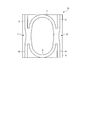
- FIG. 1 is a schematic diagram of an optical functional element according to the first embodiment.
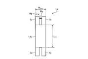
- FIG. 2A is a schematic diagram of the optical coupler shown in FIG.
- FIG. 2B is a schematic diagram of an optical coupler of a comparative form.
- FIG. 3 is a diagram showing an example of characteristics of excess loss.
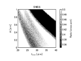
- FIG. 4 is a diagram showing an example of the characteristics of the branching ratio.
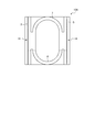
- FIG. 5 is a schematic diagram of an optical functional element according to a comparative form.
- FIG. 6 is a diagram showing an example of the characteristic of the normalized reflection port intensity.
- FIG. 7 is a schematic view of the laser device according to the second embodiment.
- FIG. 1 is a schematic diagram of an optical functional element according to the first embodiment.
- This optical functional element 10 includes the following waveguides formed on a substrate S: an optical coupler 1 which is a first optical coupler, an optical coupler 2 which is a second optical coupler, and optical input/output waveguides 3 and 4. 5 and 6, an arcuate waveguide 7 that is a first arcuate waveguide, and an arcuate waveguide 8 that is a second arcuate waveguide.
- Optical couplers 1 and 2 are 2 ⁇ 2 type, MMI waveguide type optical couplers.
- the arcuate waveguide 7 optically connects one of the input/output ports of the optical coupler 1 and one of the input/output ports of the optical coupler 2.
- the arc-shaped waveguide 8 optically connects another one of the input/output ports of the optical coupler 1 and another one of the input/output ports of the optical coupler 2.
- Optical input/output waveguides 3 and 4 are optically connected to the other two input/output ports of the optical coupler 1.
- Optical input/output waveguides 5 and 6 are optically connected to the other two input/output ports of the optical coupler 2.
- each of the arcuate waveguide 7 and the arcuate waveguide 8 is connected to each of the input/output ports facing each other in the longitudinal direction of the optical coupler 1.
- each of the arcuate waveguide 7 and the arcuate waveguide 8 is connected to each of the input/output ports facing each other in the longitudinal direction of the optical coupler 2.
- Each of the optical input/output waveguides 3 and 4 is connected to each of the input/output ports facing each other in the longitudinal direction of the optical coupler 1.
- each of the optical input/output waveguides 5 and 6 is connected to each of the input/output ports facing each other in the longitudinal direction of the optical coupler 2.
- the optical couplers 1 and 2 and the arcuate waveguides 7 and 8 form a ring resonator. Further, the optical input/output waveguides 3, 4, 5, 6 have a function of inputting/outputting light to/from this ring resonator.
- These waveguides have, for example, a waveguide structure in which an optical waveguide layer made of a semiconductor material having a higher refractive index than InP such as InGaAsP is formed in a cladding region made of InP.
- a high-mesa waveguide structure is provided.
- InP and InGaAsP are adopted for the optical function element 10 to function favorably with respect to light in the wavelength band of 1.55 ⁇ m.
- a semiconductor material corresponding to the wavelength may be appropriately adopted.
- FIG. 2A is a schematic diagram of the optical coupler 1
- FIG. 2B is a schematic diagram of the optical coupler 1A of the comparative form.
- the optical coupler 1 includes two input/output ports 1a and 1b that are first input/output ports, an MMI waveguide portion 1c, and two input/output ports 1d and 1e that are second input/output ports.
- the MMI waveguide portion 1c has end portions 1ca and 1cb that are a first end portion and a second end portion that face each other in the longitudinal direction.
- the input/output ports 1a and 1b are arranged in parallel at the end 1ca in the width direction of the MMI waveguide 1c.
- the input/output ports 1d and 1e are arranged in parallel at the end portion 1cb in the width direction of the MMI waveguide portion 1c.
- the longitudinal direction of the MMI waveguide 1c is the vertical direction in the drawing
- the width direction is the horizontal direction in the drawing orthogonal to the longitudinal direction.
- the light when light of a predetermined wavelength is input in a single mode from the input/output port 1a, the light is input to the MMI waveguide portion 1c from the end 1ca, is split into multiple modes, and is guided. Interfere with each other in the waves. As a result, the guided light is imaged in a single mode with a predetermined branching ratio at the positions connected to the input/output ports 1d and 1e of the end 1cb. As a result, the input light is split at a predetermined split ratio and output from the input/output ports 1d and 1e.
- the light is input from the input/output port 1a and the light is output from the input/output ports 1d and 1e is described here, the light is input from one of the input/output ports 1d and 1e and the input/output is performed. Light may be output from the ports 1a and 1b.
- the MMI waveguide portion 1c is composed of tapered portions 1cc and 1cd and a constant width portion 1ce.
- the tapered portion 1cc is located on the side of the input/output ports 1a and 1b, and its width is continuously reduced toward the side of the input/output ports 1d and 1e in the longitudinal direction of the MMI waveguide portion 1c.
- the tapered portion 1cc has an isosceles trapezoidal shape in a top view.
- the equal width portion 1ce is located adjacent to the input/output ports 1d and 1e of the tapered portion 1cc.
- the width of the equal width portion 1ce is substantially constant in the longitudinal direction, and is substantially the same as the width of the tapered portion 1cc on the input/output port 1d, 1e side.
- the constant width portion 1ce has a rectangular shape in a top view as shown in FIG. 2A.
- the tapered portion 1cd is located adjacent to the input/output ports 1d, 1e side of the constant width portion 1ce, and the width thereof continuously increases in the longitudinal direction of the MMI waveguide portion 1c toward the input/output ports 1d, 1e side. doing.
- the width of the tapered portion 1cd on the input/output port 1a, 1b side is substantially the same as the width of the constant width portion 1ce.
- the width of the tapered portion 1cd on the input/output ports 1d, 1e side (width at the end portion 1cb) is substantially the same as the width of the tapered portion 1cc on the input/output ports 1a, 1b side (width at the end portion 1ca). is there.
- the taper portion 1cd has an isosceles trapezoidal shape in a top view as shown in FIG. 2A.
- the taper portions 1cc and 1cd and the equal width portion 1ce are narrow width portions whose average width in the longitudinal direction is narrower than the width at the end portions 1ca and 1cb.
- the length of the MMI waveguide portion 1c is L mmi
- the width at the end portions 1ca, 1cb is W mmi
- the widths of the input/output ports 1a, 1b, 1d, 1e are Wp
- the input/output ports 1a, 1b are both Wg.
- the lengths of the tapered portions 1cc and 1cd and the equal width portion 1ce are Lt1, Lt2, and Ls, respectively. Further, the difference between W mmi and the width of the equal width portion 1ce is A.
- each of the widthwise ends of the equal width portion 1ce is at a position A/2 from either of the widthwise ends of the end portions 1ca and 1cb.
- the width of the equal width portion 1ce is (W mmi -A), and the average width in the longitudinal direction of the tapered portions 1cc and 1cd is (W mmi -A/2).
- the width (W mmi -A) of the equal width portion 1ce is, for example, 25% or more and less than 100% of W mmi .
- the length Ls of the constant width portion 1ce is, for example, a value of 10% or more of L mmi and a value of less than 100%.
- the optical function element 10 has a high degree of freedom in designing optical characteristics and has reduced excess loss because the MMI waveguide portion 1c has such a narrow width portion.
- the optical coupler 1A has a configuration in which the MMI waveguide portion 1c is replaced with the MMI waveguide portion 1Ac in the configuration of the optical coupler 1.
- the MMI waveguide portion 1Ac is a rectangular waveguide in a top view.
- the length of the MMI waveguide portion 1Ac is L mmi and the width thereof is W mmi .
- the branching ratio of the optical couplers 1 and 1A is defined by the ratio of the power of the branched light output from the input/output port 1e to the power of the input light when the light is input from the input/output port 1a. Then, when the branching ratio of the optical coupler 1A is 50%, the following formula is established. Note that n is the effective refractive index of the MMI waveguide 1Ac, and ⁇ is the wavelength of the input light.
- the relationship between L mmi and W mmi is uniquely determined, and since the FSR and finesse are also determined by this relationship, the degree of freedom in designing optical characteristics is low.
- the finesse is an amount defined by the ratio of the FSR to the full width at half maximum of the transmission peak or the reflection peak when the light transmission characteristic or the light reflection characteristic that changes periodically with respect to the wavelength is provided. The higher the finesse, the sharper the transmission peak or the reflection peak, and the higher the wavelength selectivity, for example.
- the degree of freedom in designing the optical characteristics can be increased by setting the length and width of the narrow portion.
- the degree of freedom in designing the optical characteristics of the optical functional device 10 including the optical couplers 1 and 2 can be increased.
- FIG. 3 is a diagram showing an example of characteristics of excess loss (Loss). Excess loss means that when light is input from the input/output port 1a and light branched from each of the input/output ports 1d and 1e is output, the total power of the output light with respect to the power of the input light is It is shown in dB.
- FIG. 4 is a diagram showing an example of the characteristics of the branching ratio.
- Ratio cross port
- Cross port is a branching ratio, and, for example, when light is input from the input/output port 1a, the output light from the input/output port 1e is branched for the power of the input light. Is the ratio of the power of.
- the following formula can be established while the branching ratio is other than 50%, that is, more than 0% and less than 50%, or more than 50% and less than 100%.
- n is the effective refractive index of the MMI waveguide 1c
- ⁇ is the wavelength of the input light.
- the optical functional element 10 can also be miniaturized.
- the optical characteristics of the optical functional device 10 will be described with reference to the results obtained using BMP analysis.
- the combination of A and L mmi is set so that the branching ratio of the optical couplers 1 and 2 at a predetermined wavelength is 40% for the intersecting ports. did.
- the characteristics of the optical functional element 10 as a reflective element were analyzed. Specifically, light of a predetermined wavelength was input from the optical input/output waveguide 4 of the optical functional device 10, and the power of the light output from the optical input/output waveguide 6 was analyzed. Then, the ratio of the power of the output light to the power of the input light was calculated as the normalized reflection port intensity.
- the optical functional element 10A has a configuration in which the optical couplers 1 and 2 in the configuration of the optical functional element 10 are replaced with an optical coupler 1A having a branching ratio of 50%. Then, the light was input from the optical input/output waveguide 4 of the optical functional element 10A, the power of the light output from the optical input/output waveguide 6 was analyzed, and the normalized reflection port intensity was calculated. The radii of the arcuate waveguides 7 and 8 were adjusted in each of the optical functional element 10A and the optical functional element 10 so that the optical functional element 10A and the optical functional element 10 have the same FSR.
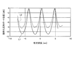
- FIG. 6 is a diagram showing an example of the characteristics of the normalized reflection port strength.
- the horizontal axis is the relative wavelength with reference to a predetermined wavelength in the wavelength band of 1.55 ⁇ m, and the vertical axis is the normalized reflection port intensity in dB.
- the solid line L1 is the reflection characteristic of the optical functional element 10
- the broken line L2 is the reflection characteristic of the optical functional element 10A.
- the optical function element 10 can have a higher finesse than the optical function element 10A. Further, in the optical function element 10, the finesse can be made lower than that of the optical function element 10A by making the branching ratio larger than 50%.
- the optical functional device 10 has a high degree of freedom in designing optical characteristics such as FSR and finesse, and has reduced excess loss.
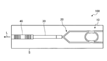
- FIG. 7 is a schematic view of the laser device according to the second embodiment.
- This laser element 100 is configured as a wavelength tunable laser element utilizing the vernier effect as disclosed in Patent Document 1.
- the laser device 100 includes optical functional devices 10, 20, 30, 40 integrated on a common substrate S. It should be noted that in FIG. 7, each heater and electrode, which will be described later, and wirings and electrode pads for supplying a current to each heater and electrode are not shown.
- the optical functional element 10 has the configuration shown in FIG. 1, and is further provided with a heater for heating the ring resonator.
- the optical function element 20 is a 1 ⁇ 2 type MMI waveguide type optical coupler, and an arm portion extending from each of two ports is optically connected to the optical function element 10, and one port is an optical function element. Optically connected to 30.
- the optical functional elements 10 and 20 have a reflection spectrum characteristic having a comb-shaped peak.
- the optical functional elements 10 and 20 constitute one of the reflectors of the laser resonator.
- a heater is provided on a part of the arm of the optical function element 20. By heating the optical waveguide layer in the arm portion with the heater, the optical path length of the optical waveguide layer can be changed. As a result, the cavity length of the laser cavity can be changed.
- the optical functional element 30 has a semiconductor laminated structure including an active layer.
- the active layer is optically connected to the 1-port side of the optical functional device 20 and the optical functional device 40.
- An electric current is supplied to the active layer by an electrode provided in the optical functional element 30 to generate an optical gain.
- the optical functional device 40 has a semiconductor laminated structure including a DBR (Distributed Bragg Reflector) type diffraction grating layer including a sampled diffraction grating (Sampled Grating) and an optical waveguide layer.
- DBR Distributed Bragg Reflector
- Sampled diffraction grating Sampled Grating
- the optical functional element 40 has a comb-shaped peak whose reflection spectrum characteristic is different from that in the optical functional elements 10 and 20, and constitutes the other one of the reflectors of the laser resonator.
- the reflection peak wavelength can be shifted as a whole on the wavelength axis.
- the laser element 100 functions as a wavelength tunable laser element utilizing the vernier effect by adjusting the current supplied to the heater and electrodes.
- the optical function element 40 as a reflector may be replaced with a reflector including the optical function elements 10 and 20.
- the two reflectors configured by the optical function elements 10 and 20 configure a laser resonator. In this case, it is necessary to make the periods of the comb-shaped reflection peaks of the two reflectors different from each other.
- the optical functional element 10 can also be combined with a reflection mirror to form a reflector having a comb-shaped reflection peak. Such a reflector can be used as a reflector in a laser cavity.
- the optical function element 10 can also be used as a wavelength selection filter.
- the width of the tapered portion changes continuously and linearly in the longitudinal direction, but may change continuously and curvilinearly, or may change in multiple steps. Good.
- the first optical coupler and the second optical coupler have substantially the same configuration, but the configurations may be different from each other.
- the MMI waveguide portion is composed of only a plurality of narrow width portions, but the MMI waveguide portion may include a portion that is not the narrow width portion.
- the MMI waveguide portion may include a uniform width portion having a width substantially the same as the width at the end portion of the MMI waveguide portion.
- the present invention is not limited to the above embodiment.
- the present invention also includes those configured by appropriately combining the constituent elements of the above-described embodiments. Further, further effects and modified examples can be easily derived by those skilled in the art. Therefore, the broader aspects of the present invention are not limited to the above embodiments, and various modifications can be made.
- the optical functional element according to the present invention is useful as a reflector of a laser resonator in a wavelength selection filter or a wavelength tunable laser element, and the laser element according to the present invention is useful as a wavelength tunable light source used for optical communication or the like. ..
Landscapes
- Physics & Mathematics (AREA)
- General Physics & Mathematics (AREA)
- Optics & Photonics (AREA)
- Condensed Matter Physics & Semiconductors (AREA)
- Electromagnetism (AREA)
- Engineering & Computer Science (AREA)
- Microelectronics & Electronic Packaging (AREA)
- Optical Integrated Circuits (AREA)
- Optical Couplings Of Light Guides (AREA)
- Semiconductor Lasers (AREA)
Abstract
光学特性の設計の自由度が高く、かつ過剰損失が低減された光機能素子を提供することを目的とする。光機能素子は、長手方向において対向する第1端部および第2端部を有する多モード干渉導波路部と、2つの第1入出力ポートと、2つの第2入出力ポートと、を有する多モード干渉導波路型の第1および第2光カプラと、第1光カプラの第1入出力ポートの一方と、第2光カプラの第1入出力ポートの一方と、を光学的に接続する第1円弧状導波路と、第1光カプラの第2入出力ポートの一方と、第2光カプラの第2入出力ポートの一方と、を光学的に接続する第2円弧状導波路と、を備え、第1光カプラ、第2光カプラ、第1円弧状導波路、および第2円弧状導波路はリング共振器を構成しており、第1光カプラおよび第2光カプラの多モード干渉導波路部は、それぞれ、第1端部または第2端部での幅よりも、長手方向における平均的な幅が狭い狭幅部を有する。
Description
本発明は、光機能素子およびレーザ素子に関する。
半導体導波路などによって構成されたリング共振器構造を有する光機能素子は、波長に対して周期的に変化する光透過特性または光反射特性を有する。このような光機能素子は、たとえば波長選択フィルタや、波長可変レーザ素子におけるレーザ共振器の反射器として用いられている(特許文献1)。リング共振器の光カプラとしては、たとえば多モード干渉(Multi-Mode Interferometer:MMI)導波路型の光カプラが用いられる。
しかしながら、公知のMMI導波路を用いて設計されたリング共振器は、その光学特性、たとえばFSR(Free Spectral Range)やフィネス(Finesse)の設計の自由度が低いという問題がある。また、MMI導波路は原理的には無損失であるが寸法ずれによる過剰損失が発生するため、特性のよいリング共振器のためにはMMI導波路における過剰損失の低減も求められている。
本発明は、上記に鑑みてなされたものであって、その目的は、光学特性の設計の自由度が高く、かつ過剰損失が低減された光機能素子およびこれを用いたレーザ素子を提供することにある。
上述した課題を解決し、目的を達成するために、本発明の一態様に係る光機能素子は、長手方向において対向する第1端部および第2端部を有する多モード干渉導波路部と、前記第1端部において幅方向に並列する2つの第1入出力ポートと、前記第2端部において幅方向に並列する2つの第2入出力ポートと、を有する多モード干渉導波路型の第1光カプラと、長手方向において第1端部および第2端部を有する多モード干渉導波路部と、前記第1端部において幅方向に並列する2つの第1入出力ポートと、前記第2端部において幅方向に並列する2つの第2入出力ポートと、を有する多モード干渉導波路型の第2光カプラと、前記第1光カプラの前記第1入出力ポートの一方と、前記第2光カプラの前記第1入出力ポートの一方と、を光学的に接続する第1円弧状導波路と、前記第1光カプラの前記第2入出力ポートの一方と、前記第2光カプラの前記第2入出力ポートの一方と、を光学的に接続する第2円弧状導波路と、を備え、前記第1光カプラ、前記第2光カプラ、前記第1円弧状導波路、および前記第2円弧状導波路はリング共振器を構成しており、前記第1光カプラおよび前記第2光カプラの多モード干渉導波路部は、それぞれ、前記第1端部または前記第2端部での幅よりも、長手方向における平均的な幅が狭い狭幅部を有することを特徴とする。
本発明の一態様に係る光機能素子は、前記第1光カプラまたは前記第2光カプラの多モード干渉導波路部の長さをLmmi、該多モード干渉導波路部の前記第1端部または前記第2端部の幅をWmmiとし、該多モード干渉導波路部の実効屈折率をnとすると、波長λにおいて以下の式が成り立つことを特徴とする。

本発明の一態様に係る光機能素子は、前記第1光カプラおよび前記第2光カプラの分岐比は0%より大きく50%未満、または50%より大きく100%未満であることを特徴とする。
本発明の一態様に係る光機能素子は、前記狭幅部は、長手方向において幅が連続的または多段階的に変化することを特徴とする。
本発明の一態様に係る光機能素子は、前記狭幅部の幅が、長手方向において略一定であり、前記第1端部または前記第2端部の幅の25%以上100%未満であることを特徴とする。
本発明の一態様に係る光機能素子は、前記狭幅部の長さが前記多モード干渉導波路部の長さの10%以上であることを特徴とする。
本発明の一態様に係るレーザ素子は、前記光機能素子を備えることを特徴とする。
本発明によれば、光学特性の設計の自由度を高く、かつ過剰損失を低減できるという効果を奏する。
以下、添付図面を参照しながら、本発明の実施形態を詳細に説明する。なお、以下に説明する実施形態により本発明が限定されるものではない。また、図面の記載において、同一または対応する要素には適宜同一の符号を付し、重複説明を適宜省略する。また、図面は模式的なものであり、各要素の寸法の関係、各要素の比率等は、現実と異なる場合があることに留意する必要がある。
(実施形態1)
図1は、実施形態1に係る光機能素子の模式図である。この光機能素子10は、基板S上に形成された以下の導波路:第1光カプラである光カプラ1と、第2光カプラである光カプラ2と、光入出力導波路3、4、5、6と、第1円弧状導波路である円弧状導波路7と、第2円弧状導波路である円弧状導波路8と、を備えている。
図1は、実施形態1に係る光機能素子の模式図である。この光機能素子10は、基板S上に形成された以下の導波路:第1光カプラである光カプラ1と、第2光カプラである光カプラ2と、光入出力導波路3、4、5、6と、第1円弧状導波路である円弧状導波路7と、第2円弧状導波路である円弧状導波路8と、を備えている。
光カプラ1、2は、2×2型であり、MMI導波路型の光カプラである。円弧状導波路7は、光カプラ1の入出力ポートの一つと、光カプラ2の入出力ポートの一つとを光学的に接続している。円弧状導波路8は、光カプラ1の入出力ポートの他の一つと、光カプラ2の入出力ポートの他の一つとを光学的に接続している。光カプラ1の他の2つの入出力ポートには光入出力導波路3、4が光学的に接続されている。光カプラ2の他の2つの入出力ポートには光入出力導波路5、6が光学的に接続されている。
具体的には、円弧状導波路7および円弧状導波路8のそれぞれは、光カプラ1の長手方向において対向する入出力ポートのそれぞれに接続している。同様に、円弧状導波路7および円弧状導波路8のそれぞれは、光カプラ2の長手方向において対向する入出力ポートのそれぞれに接続している。また、光入出力導波路3、4のそれぞれは、光カプラ1の長手方向において対向する入出力ポートのそれぞれに接続している。同様に、光入出力導波路5、6のそれぞれは、光カプラ2の長手方向において対向する入出力ポートのそれぞれに接続している。
これにより、光カプラ1、2、円弧状導波路7、8はリング共振器を構成している。また、光入出力導波路3、4、5、6は、このリング共振器に対して光を入出力させる機能を有する。
これらの導波路は、たとえば、InPからなるクラッド領域内にInGaAsPなどのInPよりも屈折率が高い半導体材料からなる光導波層が形成された導波路構造を有しており、たとえばハイメサ導波路構造を有する。なお、InPやInGaAsPは、光機能素子10が波長1.55μm帯の光に対して好適に機能するために採用されている。他の波長帯の光を導波する場合は、その波長に応じた半導体材料を適宜採用すればよい。
つぎに、光カプラ1の具体的構成について説明する。なお、光カプラ2は光カプラ1と略同一の構成なので、説明を省略する。また、以下では、光カプラ1の具体的構成を、比較形態の光カプラと対比して説明する。図2Aは、光カプラ1の模式図であり、図2Bは、比較形態の光カプラ1Aの模式図である。
光カプラ1は、第1入出力ポートである2つの入出力ポート1a、1bと、MMI導波路部1cと、第2入出力ポートである2つの入出力ポート1d、1eとを備えている。MMI導波路部1cは、長手方向において対向する第1端部および第2端部である端部1ca、1cbを有する。入出力ポート1a、1bは、端部1caにおいて、MMI導波路部1cの幅方向に並列して配置されている。入出力ポート1d、1eは、端部1cbにおいて、MMI導波路部1cの幅方向に並列して配置されている。ここで、MMI導波路部1cの長手方向は、図面の上下方向であり、幅方向は、長手方向と直交する図面の左右方向である。
たとえば、入出力ポート1aから所定の波長の光が単一モードで入力されると、当該光はMMI導波路部1cに端部1caから入力して多モードに分離して導波し、かつ導波中に互いに干渉する。その結果、導波した光は、端部1cbの入出力ポート1d、1eのそれぞれに接続する位置にて、所定の分岐比でかつシングルモードで結像する。その結果、入力された光は、所定の分岐比で分岐されて入出力ポート1d、1eから出力される。なお、ここでは、入出力ポート1aから光を入力し、入出力ポート1d、1eから光を出力させる場合について説明しているが、入出力ポート1d、1eの一方から光を入力し、入出力ポート1a、1bから光を出力させてもよい。
ここで、MMI導波路部1cは、テーパ部1cc、1cdと、等幅部1ceとで構成されている。テーパ部1ccは、入出力ポート1a、1b側に位置し、MMI導波路部1cの長手方向において入出力ポート1d、1e側に向かって幅が連続的に減少している。テーパ部1ccは図2Aに示すように上面視で等脚台形状である。
等幅部1ceは、テーパ部1ccの入出力ポート1d、1e側に隣接して位置している。等幅部1ceの幅は長手方向において略一定であり、テーパ部1ccの入出力ポート1d、1e側の幅と略同一である。等幅部1ceは図2Aに示すように上面視で矩形状である。
テーパ部1cdは、等幅部1ceの入出力ポート1d、1e側に隣接して位置し、MMI導波路部1cの長手方向において入出力ポート1d、1e側に向かって、幅が連続的に増加している。テーパ部1cdの入出力ポート1a、1b側の幅は、等幅部1ceの幅と略同一である。また、テーパ部1cdの入出力ポート1d、1e側の幅(端部1cbでの幅)は、テーパ部1ccの入出力ポート1a、1b側の幅(端部1caでの幅)と略同一である。テーパ部1cdは図2Aに示すように上面視で等脚台形状である。
テーパ部1cc、1cd、等幅部1ceは、いずれも、端部1ca、1cbでの幅よりも、長手方向における平均的な幅が狭い狭幅部である。
MMI導波路部1cの長さをLmmiとし、端部1ca、1cbでの幅をWmmiとし、入出力ポート1a、1b、1d、1eの幅をいずれもWpとし、入出力ポート1a、1b間のギャップおよび入出力ポート1d、1eのギャップをいずれもWgとする。また、テーパ部1cc、1cd、等幅部1ceの長さを、それぞれLt1、Lt2、Lsとする。また、Wmmiと等幅部1ceの幅との差をAとする。テーパ部1cc、1cdは等脚台形状なので、等幅部1ceの幅方向両端のそれぞれは、端部1ca、1cbの幅方向両端のいずれかからA/2の位置にある。等幅部1ceの幅は(Wmmi-A)であり、テーパ部1cc、1cdの長手方向における平均的な幅は(Wmmi-A/2)である。
等幅部1ceの幅(Wmmi-A)は、たとえばWmmiの25%以上100%未満である。また、等幅部1ceの長さLsは、たとえばLmmiの10%以上の値であり、100%未満の値である。
光機能素子10は、MMI導波路部1cがこのような狭幅部を有することによって、光学特性の設計の自由度が高く、かつ過剰損失が低減されたものとなる。
以下、図2Bの比較形態1に係る光カプラ1Aと対比して説明する。光カプラ1Aは、光カプラ1の構成において、MMI導波路部1cをMMI導波路部1Acに置き換えた構成を有する。MMI導波路部1Acは上面視で矩形の導波路である。ここで、光カプラ1と同様に、MMI導波路部1Acの長さをLmmi、幅をWmmiとする。
光カプラ1、1Aの分岐比を、たとえば入出力ポート1aから光を入力した場合に、入力した光のパワーに対する、分岐して入出力ポート1eから出力される光のパワーの比で定義する。すると、光カプラ1Aの分岐比が50%の場合、以下の式が成り立つ。なお、nはMMI導波路部1Acの実効屈折率であり、λは入力する光の波長である。

このように、光カプラ1Aでは、LmmiとWmmiとの関係が一義的に決定しており、かつこの関係によってFSRやフィネスも決定するため、光学特性の設計の自由度が低い。なお、フィネスとは、波長に対して周期的に変化する光透過特性または光反射特性を有する場合に、透過ピークまたは反射ピークの半値全幅に対するFSRの比で定義される量である。フィネスが高いほど透過ピークまたは反射ピークが鋭く、たとえば波長選択性が高くなる。
これに対して、光カプラ1では、MMI導波路部1cが狭幅部を有することによって、狭幅部の長さや幅の設定によって光学特性の設計の自由度を高くできる。その結果、光カプラ1、2を備える光機能素子10の光学特性の設計の自由度を高くできる。
BMP(Beam Propagation Method)解析を用いて得た結果を参照して、狭幅部の効果について説明する。以下では、Wmmiを3.15μm、Wpを1.2μm、Wgを0.75μm、Lt1、Lt2をいずれも10μmとして、LmmiとAとの組み合わせを様々に変化させて解析を行った。
図3は、過剰損失(Loss)の特性の一例を示す図である。過剰損失は、入出力ポート1aから光を入力し、入出力ポート1d、1eのそれぞれから分岐された光を出力させた場合、入力した光のパワーに対する、出力された光の合計のパワーを、dB単位で示したものである。
図3において、A=0は比較形態の光カプラ1Aの特性に相当する。図3から、LmmiとAとの組み合わせを適宜選択することによって、光カプラ1Aよりも過剰損失を低減できることが確認できる。特に、Lmmiを小さくするのに従って、Aを小さくすれば、低い過剰損失を維持したままMMI導波路部1cを長手方向に短くでき、光カプラ1を小型化できることが確認できる。
つぎに、図4は、分岐比の特性の一例を示す図である。ここで、Ratio(cross port)とは、分岐比のことであり、たとえば入出力ポート1aから光を入力した場合に、入力した光のパワーに対する、分岐して入出力ポート1eから出力される光のパワーの比である。
図4において、A=0は比較形態の光カプラ1Aの特性に相当する。図3と図4とから、分岐比を一定に維持し、かつ低い過剰損失を維持したまま、MMI導波路部1cを長手方向に短くでき、光カプラ1を小型化できることが確認できる。
以上のことから、光カプラ1では、分岐比を50%以外、すなわち0%より大きく50%未満、または50%より大きく100%未満としつつ、以下の式が成り立つようにできる。なお、nはMMI導波路部1cの実効屈折率であり、λは入力する光の波長である。

このように光カプラ1、および光カプラ2を小型化できるので、光機能素子10も小型化できる。
つぎに、光機能素子10の光学特性について、BMP解析を用いて得た結果を参照して説明する。まず、光機能素子10において、光カプラ1のBMP解析結果に基づき、所定の波長において光カプラ1、2の分岐比が交差するポートについて40%になるようにAとLmmiとの組み合わせを設定した。そして、光機能素子10の反射素子としての特性を解析した。具体的には、光機能素子10の光入出力導波路4から所定の波長の光を入力し、光入出力導波路6から出力された光のパワーを解析した。そして、入力した光のパワーに対する出力された光のパワーの比を、規格化反射ポート強度として算出した。
また、比較形態として、図5に示す構成の光機能素子10Aの特性を解析した。光機能素子10Aは、光機能素子10の構成において、光カプラ1、2を、分岐比を50%とした光カプラ1Aに置き換えた構成を有するものである。そして、光機能素子10Aの光入出力導波路4から光を入力し、光入出力導波路6から出力された光のパワーを解析し、規格化反射ポート強度を算出した。なお、円弧状導波路7、8の半径は、光機能素子10Aと光機能素子10とで同じFSRを有するように、光機能素子10Aと光機能素子10のそれぞれで調整した。
図6は、規格化反射ポート強度の特性の一例を示す図である。横軸は波長1.55μm帯の所定の波長を基準とした相対波長であり、縦軸は規格化反射ポート強度をdB単位で示したものである。実線L1が光機能素子10の反射特性であり、破線L2が光機能素子10Aの反射特性である。図6に示すように、光機能素子10では光機能素子10Aよりもフィネスを高くできることが確認された。また、光機能素子10では、分岐比を50%より大きくすることによって、光機能素子10Aよりもフィネスを低くできる。
以上説明したように、実施形態1に係る光機能素子10は、FSRやフィネスなどの光学特性の設計の自由度が高く、かつ過剰損失が低減されたものである。
(実施形態2)
図7は、実施形態2に係るレーザ素子の模式図である。このレーザ素子100は、特許文献1に開示されるようなバーニア効果を利用した波長可変型のレーザ素子として構成されている。レーザ素子100は、共通の基板S上に集積された光機能素子10、20、30、40を備えている。なお、図7では、後述する各ヒータや電極、および各ヒータや電極に電流を供給するための配線や電極パッドは図示を省略している。
図7は、実施形態2に係るレーザ素子の模式図である。このレーザ素子100は、特許文献1に開示されるようなバーニア効果を利用した波長可変型のレーザ素子として構成されている。レーザ素子100は、共通の基板S上に集積された光機能素子10、20、30、40を備えている。なお、図7では、後述する各ヒータや電極、および各ヒータや電極に電流を供給するための配線や電極パッドは図示を省略している。
光機能素子10は、図1に示す構成を有しており、さらにリング共振器を加熱するヒータが設けられている。光機能素子20は、1×2型のMMI導波路型の光カプラであり、2ポートのそれぞれから延伸するアーム部が光機能素子10に光学的に接続しており、1ポートが光機能素子30に光学的に接続している。光機能素子20の1ポートに光を入力すると、光は光機能素子10、20の機能によって反射されて、光機能素子20の1ポートから出力する。このとき、光機能素子10、20は、櫛形のピークを有する反射スペクトル特性を有している。これにより、光機能素子10、20は、レーザ共振器の反射器の一方を構成する。光機能素子10のリング共振器内の光導波層をヒータにて加熱することによって、反射ピーク波長を波長軸上で全体的にシフトさせることができる。
また、光機能素子20のアーム部の一部にもヒータが設けられている。アーム部内の光導波層をヒータにて加熱することによって、光導波層の光路長を変化させることができる。これによって、レーザ共振器の共振器長を変化させることができる。
光機能素子30は、活性層を含む半導体積層構造を有する。活性層は、光機能素子20の1ポート側と、光機能素子40とに光学的に接続している。活性層は、光機能素子30に設けられた電極によって電流が供給され光利得を発生する。
光機能素子40は、標本化回折格子(Sampled Grating)を含むDBR(Distributed Bragg Reflector)型の回折格子層と、光導波層とを含む半導体積層構造を有する。
この光機能素子40は、反射スペクトル特性が、光機能素子10、20におけるものとは周期が異なる櫛形のピークを有しており、レーザ共振器の反射器の他の一方を構成する。光機能素子40の回折格子層をヒータにて加熱することによって、反射ピーク波長を波長軸上で全体的にシフトさせることができる。
このレーザ素子100は、ヒータや電極に供給する電流を調整することによって、バーニア効果を利用した波長可変レーザ素子として機能する。
なお、レーザ素子100の構成において、反射器としての光機能素子40を、光機能素子10、20により構成される反射器に置き換えてもよい。このように構成されたレーザ素子は、光機能素子10、20により構成される2つの反射器が、レーザ共振器を構成する。この場合、2つの反射器の櫛形の反射ピークの周期を互いに異ならせる必要がある。
また、光機能素子10は、反射ミラーと組み合わせて、櫛形の反射ピークを有する反射器を構成することもできる。このような反射器は、レーザ共振器の反射器として使用することができる。また、光機能素子10は、波長選択フィルタとしても使用することもできる。
なお、上記実施形態では、テーパ部は長手方向において幅が連続的かつ直線的に変化しているが、連続的かつ曲線的に変化していてもよいし、多段階的に変化していてもよい。
また、上記実施形態では、第1光カプラと第2光カプラとが略同一の構成であるが、構成が互いに異なっていてもよい。
また、上記実施形態では、MMI導波路部は複数の狭幅部のみで構成されているが、MMI導波路部が、狭幅部ではない部分を含んでいてもよい。たとえば、MMI導波路部は、MMI導波路部の端部での幅と略同じ幅を有する等幅部を含んでいてもよい。
また、上記実施形態により本発明が限定されるものではない。上述した各実施形態の構成要素を適宜組み合わせて構成したものも本発明に含まれる。また、さらなる効果や変形例は、当業者によって容易に導き出すことができる。よって、本発明のより広範な態様は、上記の実施形態に限定されるものではなく、様々な変更が可能である。
本発明に係る光機能素子は、波長選択フィルタや波長可変レーザ素子におけるレーザ共振器の反射器に有用であり、本発明に係るレーザ素子は、光通信等に用いられる波長可変光源に有用である。
1、2 光カプラ
1a、1b、1d、1e 入出力ポート
1c MMI導波路部
1ca、1cb 端部
1cc、1cd テーパ部
1ce 等幅部
3、4、5、6 光入出力導波路
7、8 円弧状導波路
10、20、30、40 光機能素子
100 レーザ素子
L1 実線
L2 破線
S 基板
1a、1b、1d、1e 入出力ポート
1c MMI導波路部
1ca、1cb 端部
1cc、1cd テーパ部
1ce 等幅部
3、4、5、6 光入出力導波路
7、8 円弧状導波路
10、20、30、40 光機能素子
100 レーザ素子
L1 実線
L2 破線
S 基板
Claims (7)
- 長手方向において対向する第1端部および第2端部を有する多モード干渉導波路部と、前記第1端部において幅方向に並列する2つの第1入出力ポートと、前記第2端部において幅方向に並列する2つの第2入出力ポートと、を有する多モード干渉導波路型の第1光カプラと、
長手方向において第1端部および第2端部を有する多モード干渉導波路部と、前記第1端部において幅方向に並列する2つの第1入出力ポートと、前記第2端部において幅方向に並列する2つの第2入出力ポートと、を有する多モード干渉導波路型の第2光カプラと、
前記第1光カプラの前記第1入出力ポートの一方と、前記第2光カプラの前記第1入出力ポートの一方と、を光学的に接続する第1円弧状導波路と、
前記第1光カプラの前記第2入出力ポートの一方と、前記第2光カプラの前記第2入出力ポートの一方と、を光学的に接続する第2円弧状導波路と、
を備え、前記第1光カプラ、前記第2光カプラ、前記第1円弧状導波路、および前記第2円弧状導波路はリング共振器を構成しており、
前記第1光カプラおよび前記第2光カプラの多モード干渉導波路部は、それぞれ、前記第1端部または前記第2端部での幅よりも、長手方向における平均的な幅が狭い狭幅部を有する
ことを特徴とする光機能素子。 - 前記第1光カプラまたは前記第2光カプラの多モード干渉導波路部の長さをLmmi、該多モード干渉導波路部の前記第1端部または前記第2端部の幅をWmmiとし、該多モード干渉導波路部の実効屈折率をnとすると、波長λにおいて以下の式が成り立つ
ことを特徴とする請求項1に記載の光機能素子。

- 前記第1光カプラおよび前記第2光カプラの分岐比は0%より大きく50%未満、または50%より大きく100%未満である
ことを特徴とする請求項1または2に記載の光機能素子。 - 前記狭幅部は、長手方向において幅が連続的または多段階的に変化する
ことを特徴とする請求項1~3のいずれか一つに記載の光機能素子。 - 前記狭幅部の幅が、長手方向において略一定であり、前記第1端部または前記第2端部の幅の25%以上100%未満である
ことを特徴とする請求項1~4のいずれか一つに記載の光機能素子。 - 前記狭幅部の長さが前記多モード干渉導波路部の長さの10%以上である
ことを特徴とする請求項5に記載の光機能素子。 - 請求項1~6のいずれか一つに記載の光機能素子を備える
ことを特徴とするレーザ素子。
Priority Applications (3)
| Application Number | Priority Date | Filing Date | Title |
|---|---|---|---|
| JP2020571213A JPWO2020162451A1 (ja) | 2019-02-06 | 2020-02-04 | 光機能素子およびレーザ素子 |
| CN202080012607.5A CN113474955A (zh) | 2019-02-06 | 2020-02-04 | 光功能元件以及激光元件 |
| US17/392,899 US12062886B2 (en) | 2019-02-06 | 2021-08-03 | Optical functional device and laser device |
Applications Claiming Priority (2)
| Application Number | Priority Date | Filing Date | Title |
|---|---|---|---|
| JP2019-019541 | 2019-02-06 | ||
| JP2019019541 | 2019-02-06 |
Related Child Applications (1)
| Application Number | Title | Priority Date | Filing Date |
|---|---|---|---|
| US17/392,899 Continuation US12062886B2 (en) | 2019-02-06 | 2021-08-03 | Optical functional device and laser device |
Publications (1)
| Publication Number | Publication Date |
|---|---|
| WO2020162451A1 true WO2020162451A1 (ja) | 2020-08-13 |
Family
ID=71947987
Family Applications (1)
| Application Number | Title | Priority Date | Filing Date |
|---|---|---|---|
| PCT/JP2020/004120 Ceased WO2020162451A1 (ja) | 2019-02-06 | 2020-02-04 | 光機能素子およびレーザ素子 |
Country Status (4)
| Country | Link |
|---|---|
| US (1) | US12062886B2 (ja) |
| JP (1) | JPWO2020162451A1 (ja) |
| CN (1) | CN113474955A (ja) |
| WO (1) | WO2020162451A1 (ja) |
Cited By (2)
| Publication number | Priority date | Publication date | Assignee | Title |
|---|---|---|---|---|
| JPWO2022137330A1 (ja) * | 2020-12-22 | 2022-06-30 | ||
| JP2022123252A (ja) * | 2021-02-12 | 2022-08-24 | 古河電気工業株式会社 | 光半導体装置 |
Citations (10)
| Publication number | Priority date | Publication date | Assignee | Title |
|---|---|---|---|---|
| JP2000241644A (ja) * | 1998-12-22 | 2000-09-08 | Nippon Telegr & Teleph Corp <Ntt> | 多モード干渉光カプラ |
| JP2002514783A (ja) * | 1998-05-08 | 2002-05-21 | ザ トラスティーズ オブ コロンビア ユニヴァーシティ イン ザ シティ オブ ニューヨーク | 小型にした干渉に基づくマルチモードカップラ |
| US20030147432A1 (en) * | 2002-02-06 | 2003-08-07 | Jds Uniphase Corporation | Widely tunable laser |
| JP2003337236A (ja) * | 2002-05-17 | 2003-11-28 | Nec Corp | 光リング共振器、光導波路デバイスならびに光リング共振器の製造方法 |
| JP2006284791A (ja) * | 2005-03-31 | 2006-10-19 | Oki Electric Ind Co Ltd | マルチモード干渉光カプラ |
| JP2008066318A (ja) * | 2006-09-04 | 2008-03-21 | Nippon Telegr & Teleph Corp <Ntt> | 半導体波長可変レーザ |
| JP2011197069A (ja) * | 2010-03-17 | 2011-10-06 | Fujitsu Ltd | 光導波路素子及びそのような光導波路素子を備えた光受信機 |
| JP2013093627A (ja) * | 2013-02-18 | 2013-05-16 | Nippon Telegr & Teleph Corp <Ntt> | 半導体波長可変レーザ |
| JP2013168440A (ja) * | 2012-02-14 | 2013-08-29 | Japan Oclaro Inc | 半導体光変調素子及び光モジュール |
| US20150207291A1 (en) * | 2014-01-20 | 2015-07-23 | Rockley Photonics Limited | Tunable soi laser |
Family Cites Families (4)
| Publication number | Priority date | Publication date | Assignee | Title |
|---|---|---|---|---|
| US6792172B1 (en) * | 1998-05-08 | 2004-09-14 | The Trustees Of Columbia University Of The City Of New York | Reduced size multimode interference based coupler |
| WO2016152274A1 (ja) | 2015-03-20 | 2016-09-29 | 古河電気工業株式会社 | 波長可変レーザ素子およびレーザモジュール |
| JP6684094B2 (ja) | 2015-03-20 | 2020-04-22 | 古河電気工業株式会社 | 波長可変レーザ素子およびレーザモジュール |
| CN105759357B (zh) * | 2016-05-13 | 2019-09-03 | 东南大学 | 一种基于槽式波导的紧凑式模阶数转换器 |
-
2020
- 2020-02-04 CN CN202080012607.5A patent/CN113474955A/zh active Pending
- 2020-02-04 JP JP2020571213A patent/JPWO2020162451A1/ja active Pending
- 2020-02-04 WO PCT/JP2020/004120 patent/WO2020162451A1/ja not_active Ceased
-
2021
- 2021-08-03 US US17/392,899 patent/US12062886B2/en active Active
Patent Citations (10)
| Publication number | Priority date | Publication date | Assignee | Title |
|---|---|---|---|---|
| JP2002514783A (ja) * | 1998-05-08 | 2002-05-21 | ザ トラスティーズ オブ コロンビア ユニヴァーシティ イン ザ シティ オブ ニューヨーク | 小型にした干渉に基づくマルチモードカップラ |
| JP2000241644A (ja) * | 1998-12-22 | 2000-09-08 | Nippon Telegr & Teleph Corp <Ntt> | 多モード干渉光カプラ |
| US20030147432A1 (en) * | 2002-02-06 | 2003-08-07 | Jds Uniphase Corporation | Widely tunable laser |
| JP2003337236A (ja) * | 2002-05-17 | 2003-11-28 | Nec Corp | 光リング共振器、光導波路デバイスならびに光リング共振器の製造方法 |
| JP2006284791A (ja) * | 2005-03-31 | 2006-10-19 | Oki Electric Ind Co Ltd | マルチモード干渉光カプラ |
| JP2008066318A (ja) * | 2006-09-04 | 2008-03-21 | Nippon Telegr & Teleph Corp <Ntt> | 半導体波長可変レーザ |
| JP2011197069A (ja) * | 2010-03-17 | 2011-10-06 | Fujitsu Ltd | 光導波路素子及びそのような光導波路素子を備えた光受信機 |
| JP2013168440A (ja) * | 2012-02-14 | 2013-08-29 | Japan Oclaro Inc | 半導体光変調素子及び光モジュール |
| JP2013093627A (ja) * | 2013-02-18 | 2013-05-16 | Nippon Telegr & Teleph Corp <Ntt> | 半導体波長可変レーザ |
| US20150207291A1 (en) * | 2014-01-20 | 2015-07-23 | Rockley Photonics Limited | Tunable soi laser |
Cited By (4)
| Publication number | Priority date | Publication date | Assignee | Title |
|---|---|---|---|---|
| JPWO2022137330A1 (ja) * | 2020-12-22 | 2022-06-30 | ||
| JP7586194B2 (ja) | 2020-12-22 | 2024-11-19 | 日本電信電話株式会社 | 波長可変レーザ |
| JP2022123252A (ja) * | 2021-02-12 | 2022-08-24 | 古河電気工業株式会社 | 光半導体装置 |
| JP7717466B2 (ja) | 2021-02-12 | 2025-08-04 | 古河電気工業株式会社 | 光半導体装置 |
Also Published As
| Publication number | Publication date |
|---|---|
| US20210367401A1 (en) | 2021-11-25 |
| US12062886B2 (en) | 2024-08-13 |
| JPWO2020162451A1 (ja) | 2021-12-02 |
| CN113474955A (zh) | 2021-10-01 |
Similar Documents
| Publication | Publication Date | Title |
|---|---|---|
| CN113777708B (zh) | 模变换器 | |
| JP5772989B2 (ja) | レーザ素子 | |
| JP5811273B2 (ja) | 光素子、光送信素子、光受信素子、ハイブリッドレーザ、光送信装置 | |
| CN108288818B (zh) | 基于半波耦合部分反射器的可调谐半导体激光器 | |
| JP5458194B2 (ja) | 半導体波長可変レーザ | |
| JP5304158B2 (ja) | 光共振器及び波長可変レーザ | |
| JP4942429B2 (ja) | 半導体波長可変レーザ | |
| WO2013021421A1 (ja) | 半導体光素子 | |
| JP2012098472A (ja) | 光変調器 | |
| WO2019043917A1 (ja) | レーザ装置 | |
| JP2002286952A (ja) | 導波路型光カプラおよび該導波路型光カプラを用いた光合分波器 | |
| JP2013137360A (ja) | 光合分波素子およびマッハツェンダ型光変調器 | |
| US9927676B2 (en) | Optical device with integrated reflector(s) comprising a loop reflector integrating a mach-zehnder interferometer | |
| US12062886B2 (en) | Optical functional device and laser device | |
| JP2010212472A (ja) | 波長可変光源およびその発振波長の調整方法 | |
| WO2017159044A1 (ja) | 光分岐回路 | |
| JP2006284791A (ja) | マルチモード干渉光カプラ | |
| JP7095605B2 (ja) | 波長可変レーザ | |
| JP2000261086A (ja) | 波長可変光源 | |
| JP2023018261A (ja) | 波長フィルタ及びレーザ装置 | |
| JP4554209B2 (ja) | 光フィルタ | |
| JP5375620B2 (ja) | 波長可変光源 | |
| JP7608153B2 (ja) | 光学デバイスおよび光学装置 | |
| JP2750667B2 (ja) | 波長分割マルチプレクシング光通信システム用共振フィルター | |
| JP2014191088A (ja) | 光波長フィルタ |
Legal Events
| Date | Code | Title | Description |
|---|---|---|---|
| 121 | Ep: the epo has been informed by wipo that ep was designated in this application |
Ref document number: 20752813 Country of ref document: EP Kind code of ref document: A1 |
|
| ENP | Entry into the national phase |
Ref document number: 2020571213 Country of ref document: JP Kind code of ref document: A |
|
| NENP | Non-entry into the national phase |
Ref country code: DE |
|
| 122 | Ep: pct application non-entry in european phase |
Ref document number: 20752813 Country of ref document: EP Kind code of ref document: A1 |