WO2020158815A1 - 保護回路 - Google Patents
保護回路 Download PDFInfo
- Publication number
- WO2020158815A1 WO2020158815A1 PCT/JP2020/003223 JP2020003223W WO2020158815A1 WO 2020158815 A1 WO2020158815 A1 WO 2020158815A1 JP 2020003223 W JP2020003223 W JP 2020003223W WO 2020158815 A1 WO2020158815 A1 WO 2020158815A1
- Authority
- WO
- WIPO (PCT)
- Prior art keywords
- protection
- noise
- protection circuit
- battery
- circuit according
- Prior art date
- Legal status (The legal status is an assumption and is not a legal conclusion. Google has not performed a legal analysis and makes no representation as to the accuracy of the status listed.)
- Ceased
Links
Images

Classifications
-
- H—ELECTRICITY
- H02—GENERATION; CONVERSION OR DISTRIBUTION OF ELECTRIC POWER
- H02J—ELECTRIC POWER NETWORKS; CIRCUIT ARRANGEMENTS OR SYSTEMS FOR SUPPLYING OR DISTRIBUTING ELECTRIC POWER; SYSTEMS FOR STORING ELECTRIC ENERGY
- H02J7/00—Circuit arrangements for charging or discharging batteries or for supplying loads from batteries
- H02J7/60—Circuit arrangements for charging or discharging batteries or for supplying loads from batteries including safety or protection arrangements
- H02J7/663—Circuit arrangements for charging or discharging batteries or for supplying loads from batteries including safety or protection arrangements using battery or load disconnect circuits
-
- H—ELECTRICITY
- H01—ELECTRIC ELEMENTS
- H01M—PROCESSES OR MEANS, e.g. BATTERIES, FOR THE DIRECT CONVERSION OF CHEMICAL ENERGY INTO ELECTRICAL ENERGY
- H01M10/00—Secondary cells; Manufacture thereof
- H01M10/42—Methods or arrangements for servicing or maintenance of secondary cells or secondary half-cells
- H01M10/48—Accumulators combined with arrangements for measuring, testing or indicating the condition of cells, e.g. the level or density of the electrolyte
-
- G—PHYSICS
- G01—MEASURING; TESTING
- G01R—MEASURING ELECTRIC VARIABLES; MEASURING MAGNETIC VARIABLES
- G01R31/00—Arrangements for testing electric properties; Arrangements for locating electric faults; Arrangements for electrical testing characterised by what is being tested not provided for elsewhere
- G01R31/36—Arrangements for testing, measuring or monitoring the electrical condition of accumulators or electric batteries, e.g. capacity or state of charge [SoC]
- G01R31/382—Arrangements for monitoring battery or accumulator variables, e.g. SoC
- G01R31/3835—Arrangements for monitoring battery or accumulator variables, e.g. SoC involving only voltage measurements
-
- H—ELECTRICITY
- H01—ELECTRIC ELEMENTS
- H01M—PROCESSES OR MEANS, e.g. BATTERIES, FOR THE DIRECT CONVERSION OF CHEMICAL ENERGY INTO ELECTRICAL ENERGY
- H01M10/00—Secondary cells; Manufacture thereof
- H01M10/42—Methods or arrangements for servicing or maintenance of secondary cells or secondary half-cells
-
- H—ELECTRICITY
- H02—GENERATION; CONVERSION OR DISTRIBUTION OF ELECTRIC POWER
- H02H—EMERGENCY PROTECTIVE CIRCUIT ARRANGEMENTS
- H02H7/00—Emergency protective circuit arrangements specially adapted for specific types of electric machines or apparatus or for sectionalised protection of cable or line systems, and effecting automatic switching in the event of an undesired change from normal working conditions
- H02H7/18—Emergency protective circuit arrangements specially adapted for specific types of electric machines or apparatus or for sectionalised protection of cable or line systems, and effecting automatic switching in the event of an undesired change from normal working conditions for batteries; for accumulators
-
- H—ELECTRICITY
- H02—GENERATION; CONVERSION OR DISTRIBUTION OF ELECTRIC POWER
- H02J—ELECTRIC POWER NETWORKS; CIRCUIT ARRANGEMENTS OR SYSTEMS FOR SUPPLYING OR DISTRIBUTING ELECTRIC POWER; SYSTEMS FOR STORING ELECTRIC ENERGY
- H02J7/00—Circuit arrangements for charging or discharging batteries or for supplying loads from batteries
-
- Y—GENERAL TAGGING OF NEW TECHNOLOGICAL DEVELOPMENTS; GENERAL TAGGING OF CROSS-SECTIONAL TECHNOLOGIES SPANNING OVER SEVERAL SECTIONS OF THE IPC; TECHNICAL SUBJECTS COVERED BY FORMER USPC CROSS-REFERENCE ART COLLECTIONS [XRACs] AND DIGESTS
- Y02—TECHNOLOGIES OR APPLICATIONS FOR MITIGATION OR ADAPTATION AGAINST CLIMATE CHANGE
- Y02E—REDUCTION OF GREENHOUSE GAS [GHG] EMISSIONS, RELATED TO ENERGY GENERATION, TRANSMISSION OR DISTRIBUTION
- Y02E60/00—Enabling technologies; Technologies with a potential or indirect contribution to GHG emissions mitigation
- Y02E60/10—Energy storage using batteries
Definitions
- the present invention relates to a protection circuit, for example, a protection circuit provided in a charge/discharge circuit of a secondary battery.
- a protection circuit for example, a protection circuit provided in a charge/discharge circuit of a secondary battery.
- the present application claims priority based on Japanese Patent Application No. 2019-017085 filed in Japan on February 1, 2019, the content of which is incorporated herein.
- protection circuits have been implemented in mobile devices such as mobile phones and portable computers, and various devices equipped with secondary batteries, such as rechargeable electric devices.
- a protection circuit for a battery pack equipped with a lithium ion secondary battery for example, a configuration is known in which a fuse with a heater including a fuse element and a heater is connected on a charge/discharge circuit of the battery pack.
- the detection element in the event of an abnormality such as overcharging, the detection element rapidly sends an electric current to the heater, causing the heater to generate heat, and the heat causes the fuse element to melt.
- a protection circuit provided with a voltage detection IC when the voltage detection IC detects an overvoltage, a field effect transistor (FET) on the energization path of the heater is turned on, which causes the heater to generate heat,
- FET field effect transistor
- a large-capacity capacitor having a value sufficiently lower than the high-frequency internal impedance of a lithium-ion battery or an assembled battery having a value lower than the high-frequency internal impedance of a lithium-ion battery is used.
- a protection circuit for a lithium-ion battery pack which is configured by connecting in parallel with a lithium-ion battery so that the voltage is equal to or higher than the voltage (Patent Document 2).
- the noise level inside the device is lowered by releasing the noise to the outside of the device, but the noise may adversely affect not only the IC but also the human body. It is desirable to suppress noise inside the device as much as possible.
- the frequency characteristic of the noise absorbing sheet changes due to the magnetic permeability and particle size (particularly particle size) of the magnetic material. Therefore, in order to absorb low-frequency noise of about several hundred kHz, it is necessary to include a magnetic material having a large particle size in the noise absorbing sheet. Therefore, there is a problem that the thickness of the noise absorbing sheet becomes large and the device becomes large.
- An object of the present invention is to provide a protection circuit which can suppress the noise with certainty, realize the downsizing of the device with a simple configuration, and further reduce the influence of the noise on the human body.
- a protective element having a fusible metal body connected on an energization path and a heating element connected to the fusible metal body and capable of fusing the fusible metal body by heating.
- a protection device for detecting an abnormality of a device connected to the energization path, Based on the detection result of the protection device, a switching element that operates to energize the heating element of the protection element, A frequency selection element that is connected in parallel with the switching element and passes noise in a predetermined frequency band, Protection circuit with.
- the device is a battery connected to the energization path, The protection circuit according to [1], wherein the protection device detects the voltage of the battery and determines whether or not an abnormality has occurred in the battery based on the voltage.
- a protective element having a fusible metal body connected on an energization path and a heating element connected to the fusible metal body and capable of fusing the fusible metal body by heating.
- the device is a battery connected to the energization path, The protection circuit according to [6], wherein the protection device detects the voltage of the battery and determines whether or not an abnormality has occurred in the battery based on the voltage.
- the present invention it is possible to realize the miniaturization of the device with a simple configuration while reliably suppressing the noise, and further reduce the influence of the noise on the human body.
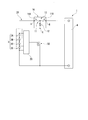
- FIG. 1 is a circuit diagram schematically showing the configuration of a protection circuit according to the first embodiment of the present invention.
- FIG. 2 is a circuit diagram schematically showing the configuration of the protection circuit according to the second embodiment of the present invention.
- FIG. 1 is a circuit diagram schematically showing the configuration of a protection circuit according to the first embodiment of the present invention.
- a battery pack protection circuit implemented in a mobile device such as a mobile phone will be described as an example.
- the protection circuit 2A is connected to the fusible metal body 11 connected to the energization path in the battery pack 1 and the fusible metal body 11, and the fusible metal body 11 can be melted by heating.
- a protection device 20 that detects an abnormality of the battery 3 (device) connected to the energization path.
- a switching element 30 that operates so as to energize 12 and a frequency selection element 40 that is connected in parallel with the switching element 30 and that passes noise in a predetermined frequency band are provided.
- the protection element 10 is connected to the external circuit at the first connection portion A, the second connection portion B, and the third connection portion C, and thereby constitutes a part of the protection circuit 2A.
- the fusible metal body 11 is connected to the energization path (charge/discharge path) of the battery 3 via the first connection portion A and the second connection portion B, and the heating element 12 is connected to the switching element 30. Is connected to the power supply path of the battery 3 via the, and the operation of the protection element 10 is controlled by the protection device 20.
- the protection element 10 is composed of, for example, a fuse with a heater.
- the fusible metal body 11 is composed of, for example, a first fuse element 11A and a second fuse element 11B connected in series on a substrate (not shown).
- the heating element 12 is connected between the first fuse element 11A and the second fuse element 11B.
- the first fuse element 11A and the second fuse element 11B are integrally formed or are formed as separate members.
- the first fuse element 11A and the second fuse element 11B are, for example, flakes or rods.
- the soluble metal body 11 is preferably a laminated body including a low melting point metal layer and a high melting point metal layer formed of a high melting point metal having a higher melting point than the low melting point metal.
- the first fuse element 11A and the second fuse element 11B are also a laminated body including a low melting point metal layer and a high melting point metal layer formed of a high melting point metal having a higher melting point than the low melting point metal.
- the fusible metal body 11 has a coating structure including a low melting point metal layer as an inner layer and a high melting point metal layer as an outer layer that covers the low melting point metal layer as the inner layer.
- the low melting point metal layer As the material forming the low melting point metal layer, various low melting point metals conventionally used as fuse materials can be used. Examples of the low melting point metal include SnSb alloy, BiSnPb alloy, BiPbSn alloy, BiPb alloy, BiSn alloy, SnPb alloy, SnAg alloy, SnAgCu alloy, PbIn alloy, ZnAl alloy, InSn alloy, and PbAgSn alloy.
- the low melting point metal layer does not necessarily have a melting point higher than the reflow temperature and may be melted at about 200°C.
- the material forming the refractory metal layer for example, Ag, Cu, or a metal containing Ag or Cu as a main component can be used.
- This high melting point metal layer has a high melting point that does not melt even when the soluble metal body 11 is mounted on an external circuit board by a reflow furnace.
- the heating element 12 is composed of a heater.
- the heater is, for example, by applying a resistance paste made of a conductive material such as ruthenium oxide or carbon black and an inorganic binder such as water glass or an organic binder such as a thermosetting resin, and firing the paste if necessary. It is formed.
- a thin film of ruthenium oxide, carbon black or the like may be formed through the steps of printing, plating, vapor deposition and sputtering, or may be formed by sticking or laminating these films.
- the protection device 20 detects the voltage of the battery 3 connected to the energization path of the protection element 10, specifically, the voltage of each of the battery cells 3A, 3B, 3C, 3D, and based on the voltage, the battery 3 (battery 3 It is determined whether or not an abnormality such as overcharge occurs in cells 3A to 3D).
- the protection device 20 operates the protection element 10 to cut off the energization path.
- the protection device 20 is connected to the switching element 30 that controls the energization operation to the protection element 10 according to the detection result of the protection device 20, and is further connected to the protection element 10 via the third connection portion C. ing. Then, the protection device 20 outputs a control signal to the switching element 30 according to the abnormality of the battery cells 3A to 3D.
- the switching element 30 is composed of, for example, a field effect transistor (hereinafter, also referred to as FET).
- FET field effect transistor
- the frequency selection element 40 is, for example, a high-pass filter, and passes the noise in the predetermined frequency range.
- the predetermined frequency band is, for example, 1 kHz to 1 GHz, and preferably 1 kHz to 1 MHz.
- the frequency selection element 40 is connected in parallel with the switching element 30 as described above, and noise in a predetermined frequency band propagates through the conduction path and reaches the frequency selection element 40.
- the battery 3 is a primary battery or a secondary battery, and examples thereof include a lithium ion secondary battery.
- a load such as a motor or a converter (not shown) is connected to the external circuit.
- the protection device 20 detects the voltage of each of the battery cells 3A to 3D and outputs a control signal to the switching element 30 when determining that any of the battery cells 3A to 3D has an abnormality such as overcharge.
- the switching element 30 operates so as to energize the heating element 12, and as a result, the heat generated by the heating element 12 causes at least one of the first fuse element 11A and the second fuse element 11B forming the fusible metal body 11. Is blown out. As a result, the power supply path of the battery cells 3A to 3D is cut off.
- noise in a predetermined frequency band propagates through the conduction path and reaches the frequency selection element 40, it passes through the frequency selection element 40 and reaches the heating element 12 of the protection element 10. Then, in the heating element 12, magnetic energy of noise in a predetermined frequency band is converted into heat energy by the heating element 12. At this time, the thermal energy generated by the heating element 12 due to noise is sufficiently lower than the thermal energy generated by the electric power supplied from the battery 3 when the abnormality of the protection device 20 is detected. Will not be blown away.
- the frequency selection element 40 since the frequency selection element 40 is connected in parallel with the switching element 30 and the noise in the predetermined frequency band passes through the frequency selection element 40, the noise that has passed through the frequency selection element 40 Reaches the heating element 12 of the protection element 10, and the noise can be absorbed by the heating element 12. Therefore, it is possible to reliably suppress the noise that adversely affects the protection device 20. Further, by providing the frequency selecting element 40 in the protection circuit 2A, noise can be easily absorbed, and it is not necessary to provide another member such as a noise absorbing sheet. In particular, even when suppressing noise in the low frequency region, it is not necessary to provide a noise absorbing sheet having a large thickness, and the protection circuit 2A and the battery pack 1 can be downsized. Further, the noise that has passed through the frequency selection element 40 is absorbed by the heating element 12, so that the noise can be suppressed inside the mobile device and the influence of the noise on the human body can be reduced.
- FIG. 2 is a circuit diagram schematically showing the configuration of the protection circuit according to the second embodiment of the present invention.
- the protection circuit according to the second embodiment is basically the same as the protection circuit 2A according to the first embodiment, and the same components are denoted by the same reference numerals and the description thereof will be omitted, and mainly different. The part will be described below.
- the protection circuit 2B includes a fusible metal body 11 connected on the energizing path, and a heating element 12 connected to the fusible metal body 11 and capable of fusing the fusible metal body 11 by heating.
- the heating element 12 of the protection element 10 is energized.
- a switching element 50 that operates.
- the switching element 50 is composed of a semiconductor element having frequency selectivity that selectively outputs noise in a predetermined frequency band.
- the predetermined frequency band is, for example, 1 kHz to 1 GHz, and preferably 1 kHz to 1 MHz.
- the semiconductor element is, for example, a FET.
- the FET is not particularly limited, but for example, a junction type FET or a MOS type FET can be used.
- the gate of the FET is connected to the protection device 20, and the drain is connected to the heating element 12.
- the FET When the semiconductor element is a FET, it is preferable that the FET is arranged near the load that is the source of noise.
- a load such as a switching type motor or converter may generate noise during switching. Therefore, by disposing an FET near such a load, it is possible to suppress the noise immediately after the generation.
- the switching element 50 is composed of a semiconductor element having a frequency selection function in addition to the switch function. Therefore, the semiconductor element selectively outputs noise in a predetermined frequency band, the noise output from the switching element 50 reaches the heating element 12 of the protection element 10, and the noise can be absorbed by the heating element 12. .. Therefore, it is possible to reduce the size of the protection circuit 2B and the battery pack 1 with a simple configuration while reliably suppressing noise, and further reduce the influence of noise on the human body. Further, the protection circuit 2B can be made to have a simpler configuration, and the protection circuit 2B and the battery pack 1 can be further downsized.
- the protection circuits 2A and 2B are applied to the battery pack 1 of a lithium ion secondary battery, but are not limited to this, and are applied to various applications that require interruption of the energization path by an electric signal. can do.
- the protection element 10 is mounted on a mobile device such as a mobile phone, the protection device 10 is not limited to this, and may be mounted on various devices including a secondary battery such as a rechargeable electric device. Further, in the protection element 10, the fusible metal body 11 is melted and blown by the heat generated by the heating element 12. However, the present invention is not limited to this. It may be fused by heat). Also with this configuration, the energization paths of the protection element 10 and the battery 3 can be cut off.
- the protection device 20 detects an abnormality of the battery 3 connected to the energization path, but is not limited to this, and may detect another device connected to the energization path.
Landscapes
- Engineering & Computer Science (AREA)
- Manufacturing & Machinery (AREA)
- Chemical & Material Sciences (AREA)
- Chemical Kinetics & Catalysis (AREA)
- Electrochemistry (AREA)
- General Chemical & Material Sciences (AREA)
- Power Engineering (AREA)
- General Physics & Mathematics (AREA)
- Physics & Mathematics (AREA)
- Charge And Discharge Circuits For Batteries Or The Like (AREA)
- Protection Of Static Devices (AREA)
- Fuses (AREA)
- Direct Current Feeding And Distribution (AREA)
- Secondary Cells (AREA)
- Control Of Motors That Do Not Use Commutators (AREA)
- Emergency Protection Circuit Devices (AREA)
- Burglar Alarm Systems (AREA)
Abstract
ノイズを確実に抑制しつつ、簡単な構成で機器の小型化を実現し、更にはノイズの人体への影響を低減することが可能な保護回路を提供する。 保護回路(2A)は、バッテリパック(1)内の通電経路上に接続された可溶金属体(11)と、可溶金属体(11)に接続され、可溶金属体(11)を加熱により溶断可能な発熱体(12)とを有する保護素子(10)と、上記通電経路に接続されたバッテリ(3)の異常を検出する保護デバイス(20)と、保護デバイス(20)の検出結果に基づいて、保護素子(10)の発熱体(12)への通電を行うように動作するスイッチング素子(30)と、スイッチング素子(30)と並列に接続され、所定の周波数帯域におけるノイズを通過させる周波数選択素子(40)とを備える。
Description
本発明は、保護回路に関し、例えば、二次電池の充放電回路に設けられる保護回路に関する。
本願は、2019年2月1日に、日本に出願された特願2019-017085に基づき優先権を主張し、その内容をここに援用する。
本願は、2019年2月1日に、日本に出願された特願2019-017085に基づき優先権を主張し、その内容をここに援用する。
従来、保護回路は、携帯電話や携帯型コンピュータなどのモバイル機器や、充電式の電動機器など、二次電池が搭載された様々な機器に実装されている。リチウムイオン二次電池を搭載したバッテリパックの保護回路として、例えばバッテリパックの充放電回路上に、ヒューズエレメントとヒーターとで構成されるヒーター付ヒューズを接続した構成が知られている。
上記保護回路において、過充電などの異常時には、検知素子がヒーターに急激に電流を流すことでヒーターが発熱し、その熱によってヒューズエレメントが溶断される。例えば、電圧検知用ICが設けられた保護回路において、電圧検知用ICが過電圧を検知したときに、ヒーターの通電経路上の電界効果トランジスタ(FET)がオンとなり、これによりヒーターが発熱し、当該ヒーターの熱によってヒューズエレメントが溶断する構成がある(特許文献1)。
ここで、ICやFETを構成する半導体は、機器内部で発生するノイズや外部から侵入するノイズによって誤動作するリスクがある。例えば、リチウムイオン電池を用いた上記のような保護回路において、過電圧を監視するための電圧検知用ICが誤動作した場合、ヒーター付ヒューズが意図せずに切れてしまい、機器が使用不能に陥る虞がある。よって、ICに悪影響を与える可能性のあるノイズを抑制するための対策を講じる必要がある。
ノイズを抑制する手段として、例えば、リチウムイオン電池の高周波内部インピーダンスよりも充分に低い値の大容量コンデンサ、又は、リチウムイオン電池の高周波内部インピ-ダンスよりも低い値の組電池を、リチウムイオン電池の電圧以上の電圧となるようにリチウムイオン電池と並列に接続して構成されるリチウムイオン電池パックの保護回路が提案されている(特許文献2)。
一般に、ノイズを抑制するための方法としては、以下の(1)~(4)が挙げられる。
(1)磁性体等を分散したノイズ吸収シートに代表される、電磁エネルギーを熱エネルギーに変換する方法
(2)金属シールドに代表される、不要輻射を反射する方法
(3)フィルターに代表される、伝送線路上のノイズを基板GNDへ排出する方法
(4)機器外部へノイズを放出する方法
(1)磁性体等を分散したノイズ吸収シートに代表される、電磁エネルギーを熱エネルギーに変換する方法
(2)金属シールドに代表される、不要輻射を反射する方法
(3)フィルターに代表される、伝送線路上のノイズを基板GNDへ排出する方法
(4)機器外部へノイズを放出する方法
しかし、上記(2),(3)の方法では、ノイズそのもののエネルギーは殆ど減衰されずに維持される為、基板GND等を介して、離れた箇所で発生したノイズが周り込むことがあり、結果的に機器全体としてノイズを抑制することができない場合がある。よって、特許文献2においてコンデンサを設ける構成では、ノイズをGNDに排出するため、ノイズを確実に抑制することができず、また、組電池を設ける構成では、機器が大型化するという問題がある。
また、上記(4)の方法では、ノイズを機器外部へ放出することで機器内部のノイズレベルは低下するが、ノイズはICのみならず、人体に対しても悪影響を及ぼす虞があることから、できる限り機器内部でノイズを抑制することが望ましい。
また、上記(1)の方法、すなわちノイズを熱エネルギーに変換するノイズ吸収シートを用いる方法では、磁性体の透磁率や粒径(特に粒径)に因ってノイズ吸収シートの周波数特性が変わるため、数百kHz程度の低周波ノイズを吸収するためには、粒径の大きい磁性体をノイズ吸収シートに含有させる必要がある。よって、ノイズ吸収シートの厚さが大きくなり、機器が大型化するという問題がある。
本発明の目的は、ノイズを確実に抑制しつつ、簡単な構成で機器の小型化を実現し、更にはノイズの人体への影響を低減することが可能な保護回路を提供することにある。
上記目的を達成するために、本発明は以下の手段を提供する。
[1]通電経路上に接続された可溶金属体と、前記可溶金属体に接続され、前記可溶金属体を加熱により溶断可能な発熱体とを有する保護素子と、
前記通電経路に接続された機器の異常を検出する保護デバイスと、
前記保護デバイスの検出結果に基づいて、前記保護素子の前記発熱体への通電を行うように動作するスイッチング素子と、
前記スイッチング素子と並列に接続され、所定の周波数帯域におけるノイズを通過する周波数選択素子と、
を備える保護回路。
[2]前記所定の周波数帯域は、1kHz~1GHzである、上記[1]に記載の保護回路。
[3]前記所定の周波数帯域におけるノイズの磁気エネルギーが、前記発熱体で熱エネルギーに変換される、上記[1]または[2]に記載の保護回路。
[4]前記周波数選択素子は、ハイパスフィルタである、上記[1]に記載の保護回路。
[5]前記機器は、前記通電経路に接続されたバッテリであり、
前記保護デバイスは、前記バッテリの電圧を検出し、前記電圧に基づいて前記バッテリに異常が生じているか否かを判別する、上記[1]に記載の保護回路。
[6]通電経路上に接続された可溶金属体と、前記可溶金属体に接続され、前記可溶金属体を加熱により溶断可能な発熱体とを有する保護素子と、
前記通電経路に接続された機器の異常を検出する保護デバイスと、
前記保護デバイスの検出結果に基づいて、前記保護素子の前記発熱体への通電を行うように動作するスイッチング素子と、
を備え、
前記スイッチング素子は、所定の周波数帯域のノイズを選択的に出力する周波数選択性を有する半導体素子で構成される、上記[1]に記載の保護回路。
[7]前記所定の周波数帯域は、1kHz~1GHzである、上記[6]に記載の保護回路。
[8]前記所定の周波数帯域におけるノイズの磁気エネルギーが、前記発熱体で熱エネルギーに変換される、上記[6]または[7]に記載の保護回路。
[9]前記半導体素子は、電界効果トランジスタである、上記[6]に記載の保護回路。
[10]前記機器は、前記通電経路に接続されたバッテリであり、
前記保護デバイスは、前記バッテリの電圧を検出し、前記電圧に基づいて前記バッテリに異常が生じているか否かを判別する、上記[6]に記載の保護回路。
[1]通電経路上に接続された可溶金属体と、前記可溶金属体に接続され、前記可溶金属体を加熱により溶断可能な発熱体とを有する保護素子と、
前記通電経路に接続された機器の異常を検出する保護デバイスと、
前記保護デバイスの検出結果に基づいて、前記保護素子の前記発熱体への通電を行うように動作するスイッチング素子と、
前記スイッチング素子と並列に接続され、所定の周波数帯域におけるノイズを通過する周波数選択素子と、
を備える保護回路。
[2]前記所定の周波数帯域は、1kHz~1GHzである、上記[1]に記載の保護回路。
[3]前記所定の周波数帯域におけるノイズの磁気エネルギーが、前記発熱体で熱エネルギーに変換される、上記[1]または[2]に記載の保護回路。
[4]前記周波数選択素子は、ハイパスフィルタである、上記[1]に記載の保護回路。
[5]前記機器は、前記通電経路に接続されたバッテリであり、
前記保護デバイスは、前記バッテリの電圧を検出し、前記電圧に基づいて前記バッテリに異常が生じているか否かを判別する、上記[1]に記載の保護回路。
[6]通電経路上に接続された可溶金属体と、前記可溶金属体に接続され、前記可溶金属体を加熱により溶断可能な発熱体とを有する保護素子と、
前記通電経路に接続された機器の異常を検出する保護デバイスと、
前記保護デバイスの検出結果に基づいて、前記保護素子の前記発熱体への通電を行うように動作するスイッチング素子と、
を備え、
前記スイッチング素子は、所定の周波数帯域のノイズを選択的に出力する周波数選択性を有する半導体素子で構成される、上記[1]に記載の保護回路。
[7]前記所定の周波数帯域は、1kHz~1GHzである、上記[6]に記載の保護回路。
[8]前記所定の周波数帯域におけるノイズの磁気エネルギーが、前記発熱体で熱エネルギーに変換される、上記[6]または[7]に記載の保護回路。
[9]前記半導体素子は、電界効果トランジスタである、上記[6]に記載の保護回路。
[10]前記機器は、前記通電経路に接続されたバッテリであり、
前記保護デバイスは、前記バッテリの電圧を検出し、前記電圧に基づいて前記バッテリに異常が生じているか否かを判別する、上記[6]に記載の保護回路。
本発明によれば、ノイズを確実に抑制しつつ、簡単な構成で機器の小型化を実現し、更にはノイズの人体への影響を低減することができる。
以下、本発明の実施形態について、図面を参照して詳細に説明する。
図1は、本発明の第1実施形態に係る保護回路の構成を概略的に示す回路図である。本実施形態では、携帯電話などのモバイル機器に実装されるバッテリパックの保護回路を例に挙げて説明する。
図1に示すように、保護回路2Aは、バッテリパック1内の通電経路上に接続された可溶金属体11と、可溶金属体11に接続され、可溶金属体11を加熱により溶断可能な発熱体12とを有する保護素子10と、上記通電経路に接続されたバッテリ3(機器)の異常を検出する保護デバイス20と、保護デバイス20の検出結果に基づいて、保護素子10の発熱体12への通電を行うように動作するスイッチング素子30と、スイッチング素子30と並列に接続され、所定の周波数帯域におけるノイズを通過させる周波数選択素子40とを備える。
保護素子10は、第1接続部A、第2接続部Bおよび第3接続部Cで外部回路に接続されており、これにより保護回路2Aの一部を構成している。この保護素子10では、可溶金属体11は、第1接続部Aおよび第2接続部Bを介してバッテリ3の通電経路(充放電経路)に接続されると共に、発熱体12がスイッチング素子30を介してバッテリ3の給電経路に接続されており、保護素子10の動作が保護デバイス20によって制御される。保護素子10は、例えばヒーター付きヒューズで構成されている。
可溶金属体11は、例えば、不図示の基板上で直列接続された第1ヒューズエレメント11Aおよび第2ヒューズエレメント11Bで構成されている。発熱体12は、第1ヒューズエレメント11Aと第2ヒューズエレメント11Bとの間に接続されている。
第1ヒューズエレメント11Aおよび第2ヒューズエレメント11Bは、一体で形成されるか、または別部材で構成されている。第1ヒューズエレメント11Aおよび第2ヒューズエレメント11Bは、例えば薄片状あるいは棒状である。
可溶金属体11は、低融点金属層と、該低融点金属よりも融点の高い高融点金属で構成された高融点金属層とを含む積層体であるのが好ましい。この場合、第1ヒューズエレメント11Aおよび第2ヒューズエレメント11Bも、低融点金属層と、該低融点金属よりも融点の高い高融点金属で構成された高融点金属層とを含む積層体である。また、可溶金属体11は、内層としての低融点金属層と、上記内層としての低融点金属層を被覆する外層としての高融点金属層とで構成される被覆構造を有するのがより好ましい。
上記低融点金属層を構成する材料は、従来からヒューズ材料として使用されている種々の低融点金属を用いることができる。低融点金属としては、SnSb合金、BiSnPb合金、BiPbSn合金、BiPb合金、BiSn合金、SnPb合金、SnAg合金、SnAgCu合金、PbIn合金、ZnAl合金、InSn合金、PbAgSn合金等を挙げることができる。低融点金属層は、必ずしもリフロー温度よりも高い融点を有する必要はなく、200℃程度で溶融してもよい。
上記高融点金属層を構成する材料は、例えば、Ag、Cu、または、Ag若しくはCuを主成分とする金属を用いることができる。この高融点金属層は、可溶金属体11をリフロー炉によって外部回路基板上に実装する場合においても溶融しない高い融点を有する。
発熱体12は、ヒーターで構成される。ヒーターは、例えば、酸化ルテニウムやカーボンブラック等の導電材料と、水ガラス等の無機系バインダや熱硬化性樹脂等の有機系バインダとからなる抵抗ペーストを塗布し、必要に応じて焼成することによって形成される。
また、ヒーターとしては、酸化ルテニウムやカーボンブラック等の薄膜を、印刷、メッキ、蒸着、スパッタの工程を経て形成してもよく、これらフィルムの貼付や積層等によって形成してもよい。
また、ヒーターとしては、酸化ルテニウムやカーボンブラック等の薄膜を、印刷、メッキ、蒸着、スパッタの工程を経て形成してもよく、これらフィルムの貼付や積層等によって形成してもよい。
保護デバイス20は、保護素子10の通電経路に接続されたバッテリ3の電圧、具体的にはバッテリセル3A,3B,3C,3Dの各々の電圧を検出し、該電圧に基づいてバッテリ3(バッテリセル3A~3D)に過充電などの異常が生じたか否かを判別する。バッテリセル3A~3Dで異常が生じた場合には、保護デバイス20は、保護素子10を作動させることにより通電経路を遮断する。
保護デバイス20は、該保護デバイス20の検出結果に応じて保護素子10への通電動作を制御するスイッチング素子30と接続されており、更に、第3接続部Cを介して保護素子10と接続されている。そして、保護デバイス20は、バッテリセル3A~3Dの異常に応じて制御信号をスイッチング素子30に出力する。
保護デバイス20は、該保護デバイス20の検出結果に応じて保護素子10への通電動作を制御するスイッチング素子30と接続されており、更に、第3接続部Cを介して保護素子10と接続されている。そして、保護デバイス20は、バッテリセル3A~3Dの異常に応じて制御信号をスイッチング素子30に出力する。
スイッチング素子30は、例えば電界効果トランジスタ(以下、FETともいう)で構成されている。スイッチング素子30は、保護デバイス20から出力される制御信号によって、バッテリセル3A~3Dの電圧が過放電又は過充電状態を示す所定値以上であるときに、保護素子10に通電させてバッテリ3の通電経路を遮断するように動作する。
周波数選択素子40は、例えばハイパスフィルタであり、上記所定の周波数領域におけるノイズを通過する。所定の周波数帯域は、例えば1kHz~1GHzであり、好ましくは1kHz~1MHzである。周波数選択素子40は、上述のようにスイッチング素子30と並列に接続されており、所定の周波数帯域におけるノイズが通電経路を伝搬して周波数選択素子40に到達する。
上記のように構成される保護回路2Aにおいて、バッテリ3の充電時には、充電装置4から外部回路を介してバッテリ3に電力が供給される。また、バッテリ3の放電時には、バッテリ3から外部回路に電力が供給される。バッテリ3は、一次電池あるいは二次電池であり、例えばリチウムイオン二次電池などが挙げられる。外部回路には、例えば不図示のモーターやコンバータなどの負荷が接続される。
保護デバイス20は、バッテリセル3A~3Dの各々の電圧を検出し、バッテリセル3A~3Dのいずれかに過充電などの異常が生じたと判別したときは、スイッチング素子30へ制御信号を出力する。これにより、スイッチング素子30は発熱体12に通電するように動作し、その結果、発熱体12の発熱によって、可溶金属体11を構成する第1ヒューズエレメント11Aおよび第2ヒューズエレメント11Bの少なくとも一方が溶断される。これにより、バッテリセル3A~3Dの通電経路が遮断される。
また、所定の周波数帯域におけるノイズが通電経路を伝搬して周波数選択素子40に到達すると、周波数選択素子40を通過し、保護素子10の発熱体12に到達する。そして、発熱体12において、所定の周波数帯域におけるノイズの磁気エネルギーが、発熱体12によって熱エネルギーに変換される。このとき、ノイズによって発熱体12で発生する熱エネルギーは、保護デバイス20の異常検出時にバッテリ3から供給される電力によって発生する熱エネルギーよりも十分に低いため、保護素子10の可溶金属体11が溶断されることは無い。
上述したように、本実施形態によれば、周波数選択素子40がスイッチング素子30と並列に接続され、所定の周波数帯域におけるノイズが周波数選択素子40を通過するので、周波数選択素子40を通過したノイズが保護素子10の発熱体12に到達し、当該ノイズを発熱体12で吸収することができる。よって、保護デバイス20に悪影響を及ぼすノイズを確実に抑制することが可能となる。また、保護回路2Aに周波数選択素子40を設けることで簡単にノイズを吸収することができ、ノイズ吸収シート等の他の部材を設ける必要がない。特に、低周波領域におけるノイズを抑制する場合であっても、厚さの大きいノイズ吸収シートを設ける必要が無く、保護回路2Aやバッテリパック1を小型化することが可能となる。更に、周波数選択素子40を通過したノイズが発熱体12で吸収されるので、モバイル機器の内部でノイズを抑制することができ、ノイズの人体への影響を低減することが可能となる。
図2は、本発明の第2実施形態に係る保護回路の構成を概略的に示す回路図である。本第2実施形態に係る保護回路は、第1実施形態に係る保護回路2Aと基本的に同じであり、同一の構成要素には、同一番号を付してその説明を省略し、主に異なる部分を以下に説明する。
図2に示すように、保護回路2Bは、通電経路上に接続された可溶金属体11と、可溶金属体11に接続され、可溶金属体11を加熱により溶断可能な発熱体12とを有する保護素子10と、上記通電経路に接続されたバッテリ3の異常を検出する保護デバイス20と、保護デバイス20の検出結果に基づいて、保護素子10の発熱体12への通電を行うように動作するスイッチング素子50とを備える。
スイッチング素子50は、所定の周波数帯域のノイズを選択的に出力する周波数選択性を有する半導体素子で構成されている。所定の周波数帯域は、例えば1kHz~1GHzであり、好ましくは1kHz~1MHzである。半導体素子は、例えばFETである。FETとしては、特に制限は無いが、例えば接合型FETやMOS型FETを用いることができる。本実施形態では、FETのゲートが保護デバイス20に接続され、ドレインが発熱体12に接続されている。
半導体素子がFETである場合、FETは、ノイズの発生源となる負荷の近傍に配置されるのが好ましい。スイッチング方式のモーターやコンバータなどの負荷は、スイッチング時にノイズが発生する場合があるため、このような負荷の近傍にFETを配置することで、発生直後のノイズを抑制することが可能となる。
本第2実施形態によれば、スイッチング素子50が、スイッチ機能に加えて周波数選択機能を有する半導体素子で構成されている。よって、半導体素子によって所定の周波数帯域のノイズが選択的に出力され、スイッチング素子50から出力されたノイズが保護素子10の発熱体12に到達し、当該ノイズを発熱体12で吸収することができる。したがって、ノイズを確実に抑制しつつ、簡単な構成で保護回路2Bやバッテリパック1の小型化を実現し、更にはノイズの人体への影響を低減することができる。また、保護回路2Bをより簡単な構成とすることができ、保護回路2Bやバッテリパック1を更に小型化することが可能となる。
以上、本発明の実施形態について詳述したが、本発明は上記実施形態に限定されるものではなく、特許請求の範囲内に記載された本発明の要旨の範囲内において、種々の変形・変更が可能である。
例えば、上記実施形態では、保護回路2A,2Bは、リチウムイオン二次電池のバッテリパック1に適用されるが、これに限らず、電気信号による通電経路の遮断を必要とする様々な用途に適用することができる。
保護素子10は、携帯電話などのモバイル機器に実装されるが、これに限らず、充電式の電動機器など、二次電池が搭載された様々な機器に実装されてもよい。
また、保護素子10では、発熱体12の発熱によって可溶金属体11が溶断されるが、これに限らず、通電経路が過電流となった場合に、可溶金属体11が自己発熱(ジュール熱)により溶断されてもよい。本構成によっても、保護素子10やバッテリ3の通電経路を遮断することができる。
また、保護素子10では、発熱体12の発熱によって可溶金属体11が溶断されるが、これに限らず、通電経路が過電流となった場合に、可溶金属体11が自己発熱(ジュール熱)により溶断されてもよい。本構成によっても、保護素子10やバッテリ3の通電経路を遮断することができる。
保護デバイス20は、通電経路に接続されたバッテリ3の異常を検出するが、これに限らず、上記通電経路に接続された他の機器を検出してもよい。
1 バッテリパック
2A 保護回路
2B 保護回路
3 バッテリ
3A バッテリセル
3B バッテリセル
3C バッテリセル
3D バッテリセル
4 充電装置
10 保護素子
11 可溶金属体
11A 第1ヒューズエレメント
11B 第2ヒューズエレメント
12 発熱体
20 保護デバイス
30 スイッチング素子
40 周波数選択素子
50 スイッチング素子
2A 保護回路
2B 保護回路
3 バッテリ
3A バッテリセル
3B バッテリセル
3C バッテリセル
3D バッテリセル
4 充電装置
10 保護素子
11 可溶金属体
11A 第1ヒューズエレメント
11B 第2ヒューズエレメント
12 発熱体
20 保護デバイス
30 スイッチング素子
40 周波数選択素子
50 スイッチング素子
Claims (10)
- 通電経路上に接続された可溶金属体と、前記可溶金属体に接続され、前記可溶金属体を加熱により溶断可能な発熱体とを有する保護素子と、
前記通電経路に接続された機器の異常を検出する保護デバイスと、
前記保護デバイスの検出結果に基づいて、前記保護素子の前記発熱体への通電を行うように動作するスイッチング素子と、
前記スイッチング素子と並列に接続され、所定の周波数帯域におけるノイズを通過する周波数選択素子と、
を備える保護回路。 - 前記所定の周波数帯域は、1kHz~1GHzである、請求項1に記載の保護回路。
- 前記所定の周波数帯域におけるノイズの磁気エネルギーが、前記発熱体で熱エネルギーに変換される、請求項1または2に記載の保護回路。
- 前記周波数選択素子は、ハイパスフィルタである、請求項1に記載の保護回路。
- 前記機器は、前記通電経路に接続されたバッテリであり、
前記保護デバイスは、前記バッテリの電圧を検出し、前記電圧に基づいて前記バッテリに異常が生じているか否かを判別する、請求項1に記載の保護回路。 - 通電経路上に接続された可溶金属体と、前記可溶金属体に接続され、前記可溶金属体を加熱により溶断可能な発熱体とを有する保護素子と、
前記通電経路に接続された機器の異常を検出する保護デバイスと、
前記保護デバイスの検出結果に基づいて、前記保護素子の前記発熱体への通電を行うように動作するスイッチング素子と、
を備え、
前記スイッチング素子は、所定の周波数帯域におけるノイズを選択的に出力する周波数選択性を有する半導体素子で構成される、請求項1に記載の保護回路。 - 前記所定の周波数帯域は、1kHz~1GHzである、請求項6に記載の保護回路。
- 前記所定の周波数帯域におけるノイズの磁気エネルギーが、前記発熱体で熱エネルギーに変換される、請求項6または7に記載の保護回路。
- 前記半導体素子は、電界効果トランジスタである、請求項6に記載の保護回路。
- 前記機器は、前記通電経路に接続されたバッテリであり、
前記保護デバイスは、前記バッテリの電圧を検出し、前記電圧に基づいて前記バッテリに異常が生じているか否かを判別する、請求項6に記載の保護回路。
Priority Applications (2)
| Application Number | Priority Date | Filing Date | Title |
|---|---|---|---|
| CN202080010860.7A CN113366721B (zh) | 2019-02-01 | 2020-01-29 | 保护电路 |
| KR1020217023295A KR102587483B1 (ko) | 2019-02-01 | 2020-01-29 | 보호 회로 |
Applications Claiming Priority (2)
| Application Number | Priority Date | Filing Date | Title |
|---|---|---|---|
| JP2019017085A JP7129355B2 (ja) | 2019-02-01 | 2019-02-01 | 保護回路 |
| JP2019-017085 | 2019-02-01 |
Publications (1)
| Publication Number | Publication Date |
|---|---|
| WO2020158815A1 true WO2020158815A1 (ja) | 2020-08-06 |
Family
ID=71841356
Family Applications (1)
| Application Number | Title | Priority Date | Filing Date |
|---|---|---|---|
| PCT/JP2020/003223 Ceased WO2020158815A1 (ja) | 2019-02-01 | 2020-01-29 | 保護回路 |
Country Status (5)
| Country | Link |
|---|---|
| JP (1) | JP7129355B2 (ja) |
| KR (1) | KR102587483B1 (ja) |
| CN (1) | CN113366721B (ja) |
| TW (1) | TWI813855B (ja) |
| WO (1) | WO2020158815A1 (ja) |
Families Citing this family (1)
| Publication number | Priority date | Publication date | Assignee | Title |
|---|---|---|---|---|
| KR102923815B1 (ko) * | 2022-02-23 | 2026-02-05 | 현대모비스 주식회사 | 배터리 셀 전압 측정 회로 및 그 제어 방법 |
Citations (3)
| Publication number | Priority date | Publication date | Assignee | Title |
|---|---|---|---|---|
| JP2000067928A (ja) * | 1998-08-26 | 2000-03-03 | Sony Corp | 電池保護回路及び電子装置 |
| JP2010200598A (ja) * | 2009-02-24 | 2010-09-09 | Samsung Sdi Co Ltd | バッテリパックおよび過放電保護方法 |
| JP2014102968A (ja) * | 2012-11-20 | 2014-06-05 | Sanyo Electric Co Ltd | 電池パックとその製造方法 |
Family Cites Families (18)
| Publication number | Priority date | Publication date | Assignee | Title |
|---|---|---|---|---|
| JPH0945375A (ja) | 1995-08-01 | 1997-02-14 | Shindengen Electric Mfg Co Ltd | リチウムイオン電池パック |
| JPH1051962A (ja) * | 1996-08-02 | 1998-02-20 | Sony Corp | 過充電保護回路及び方法並びに電池パック |
| WO2005038952A2 (en) * | 2003-10-14 | 2005-04-28 | Black & Decker Inc. | Protection methods, protection circuits and protective devices for secondary batteries, a power tool, charger and battery pack adapted to provide protection against fault conditions in the battery pack |
| JP4207877B2 (ja) * | 2004-10-04 | 2009-01-14 | ソニーケミカル&インフォメーションデバイス株式会社 | 保護回路 |
| JP4682643B2 (ja) * | 2005-02-24 | 2011-05-11 | ミツミ電機株式会社 | 保護回路及び保護方法 |
| US7952330B2 (en) * | 2005-04-20 | 2011-05-31 | Panasonic Corporation | Secondary battery protection circuit, battery pack and thermosensitive protection switch device |
| CN101507112A (zh) * | 2006-08-15 | 2009-08-12 | 沙夫纳Emv股份公司 | 低泄漏emc滤波器 |
| CN101159378A (zh) * | 2007-07-27 | 2008-04-09 | 张庭炎 | 一种变压器及供电线路的防雷方法及装置 |
| KR100938080B1 (ko) * | 2007-09-28 | 2010-01-21 | 삼성에스디아이 주식회사 | 안전 회로 및 이를 이용한 배터리 팩 |
| JP4771096B2 (ja) | 2008-06-02 | 2011-09-14 | ソニーケミカル&インフォメーションデバイス株式会社 | 保護回路 |
| JP5415318B2 (ja) * | 2010-02-19 | 2014-02-12 | デクセリアルズ株式会社 | 保護回路、バッテリ制御装置、及び、バッテリパック |
| EA022682B1 (ru) * | 2010-03-05 | 2016-02-29 | Амбиент Корпорейшн | Оценка уровня помех и избыточного тока в линии электропередачи |
| DE102011076877A1 (de) * | 2011-06-01 | 2012-12-06 | Siemens Aktiengesellschaft | Adaptiver Netzfilter |
| CN202142843U (zh) * | 2011-07-12 | 2012-02-08 | 广州明美电子有限公司 | 一种双节电池电量的计量及保护电路 |
| US8970323B2 (en) * | 2011-07-19 | 2015-03-03 | Infineon Technologies Ag | Circuit arrangement with an antenna switch and a bandstop filter and corresponding method |
| JP6277057B2 (ja) * | 2014-05-13 | 2018-02-07 | デクセリアルズ株式会社 | バッテリパック、バッテリシステム、及び放電方法 |
| CN104538963B (zh) * | 2014-11-13 | 2017-04-19 | 美国环境电力公司 | 自适应滤波器 |
| US10784675B2 (en) * | 2016-07-19 | 2020-09-22 | Drive Creek Llc | Vehicle accessory power switch |
-
2019
- 2019-02-01 JP JP2019017085A patent/JP7129355B2/ja active Active
-
2020
- 2020-01-29 WO PCT/JP2020/003223 patent/WO2020158815A1/ja not_active Ceased
- 2020-01-29 KR KR1020217023295A patent/KR102587483B1/ko active Active
- 2020-01-29 CN CN202080010860.7A patent/CN113366721B/zh active Active
- 2020-01-31 TW TW109103065A patent/TWI813855B/zh active
Patent Citations (3)
| Publication number | Priority date | Publication date | Assignee | Title |
|---|---|---|---|---|
| JP2000067928A (ja) * | 1998-08-26 | 2000-03-03 | Sony Corp | 電池保護回路及び電子装置 |
| JP2010200598A (ja) * | 2009-02-24 | 2010-09-09 | Samsung Sdi Co Ltd | バッテリパックおよび過放電保護方法 |
| JP2014102968A (ja) * | 2012-11-20 | 2014-06-05 | Sanyo Electric Co Ltd | 電池パックとその製造方法 |
Also Published As
| Publication number | Publication date |
|---|---|
| CN113366721A (zh) | 2021-09-07 |
| TW202037028A (zh) | 2020-10-01 |
| JP7129355B2 (ja) | 2022-09-01 |
| KR20210102442A (ko) | 2021-08-19 |
| KR102587483B1 (ko) | 2023-10-11 |
| CN113366721B (zh) | 2024-11-08 |
| JP2020127258A (ja) | 2020-08-20 |
| TWI813855B (zh) | 2023-09-01 |
Similar Documents
| Publication | Publication Date | Title |
|---|---|---|
| US8049469B2 (en) | Safety circuit and battery pack using the same | |
| US5853908A (en) | Protective device for secondary batteries | |
| JP5504193B2 (ja) | 二次電池パック及び二次電池パック用保護回路モジュール | |
| US9640789B2 (en) | Connecting element for secondary battery and secondary battery comprising the same | |
| KR101601135B1 (ko) | 이차전지 및 이에 적용되는 전극 리드 조립체 | |
| US9923362B2 (en) | Protective device | |
| WO2012147598A1 (ja) | 充放電制御装置、バッテリパック、電気機器及び充放電制御方法 | |
| JP5952674B2 (ja) | 保護素子及びバッテリパック | |
| WO2006121290A1 (en) | Protection circuit for secondary battery and secondary battery comprising the same | |
| WO2016017567A1 (ja) | 保護素子及び保護回路 | |
| JP2016073022A (ja) | 二次電池保護回路およびバッテリ装置 | |
| KR102043051B1 (ko) | 보호 소자 | |
| JP7129355B2 (ja) | 保護回路 | |
| WO2016190078A1 (ja) | 保護素子、ヒューズ素子 | |
| TWI233228B (en) | Secondary batteries having a bypass resistance and the protective method of the secondary battery | |
| WO2020189225A1 (ja) | バッテリパック、保護回路 | |
| WO2015037210A1 (ja) | 切替回路 | |
| JP2004103483A (ja) | バッテリパック | |
| US7652860B2 (en) | Polymer PTC device | |
| JP2008171662A (ja) | 電池パック | |
| WO2022181652A1 (ja) | 保護素子及びバッテリパック | |
| JP2003070153A (ja) | 二次電池パックの過昇温防止方法 | |
| JP7334870B2 (ja) | 電池モジュール、電池モジュールの製造方法、電子機器および電動車両 | |
| CN220796636U (zh) | 一种高压熔断器组合 | |
| JP5187725B2 (ja) | 電池パック |
Legal Events
| Date | Code | Title | Description |
|---|---|---|---|
| 121 | Ep: the epo has been informed by wipo that ep was designated in this application |
Ref document number: 20749597 Country of ref document: EP Kind code of ref document: A1 |
|
| ENP | Entry into the national phase |
Ref document number: 20217023295 Country of ref document: KR Kind code of ref document: A |
|
| NENP | Non-entry into the national phase |
Ref country code: DE |
|
| 122 | Ep: pct application non-entry in european phase |
Ref document number: 20749597 Country of ref document: EP Kind code of ref document: A1 |