WO2020153499A1 - 半導体ウェハ加工用紫外線硬化型粘着テープ及び半導体チップの製造方法並びにこのテープの使用方法 - Google Patents
半導体ウェハ加工用紫外線硬化型粘着テープ及び半導体チップの製造方法並びにこのテープの使用方法 Download PDFInfo
- Publication number
- WO2020153499A1 WO2020153499A1 PCT/JP2020/002617 JP2020002617W WO2020153499A1 WO 2020153499 A1 WO2020153499 A1 WO 2020153499A1 JP 2020002617 W JP2020002617 W JP 2020002617W WO 2020153499 A1 WO2020153499 A1 WO 2020153499A1
- Authority
- WO
- WIPO (PCT)
- Prior art keywords
- ultraviolet
- semiconductor wafer
- adhesive tape
- tape
- curable
- Prior art date
- Legal status (The legal status is an assumption and is not a legal conclusion. Google has not performed a legal analysis and makes no representation as to the accuracy of the status listed.)
- Ceased
Links
Images
Classifications
-
- C—CHEMISTRY; METALLURGY
- C09—DYES; PAINTS; POLISHES; NATURAL RESINS; ADHESIVES; COMPOSITIONS NOT OTHERWISE PROVIDED FOR; APPLICATIONS OF MATERIALS NOT OTHERWISE PROVIDED FOR
- C09J—ADHESIVES; NON-MECHANICAL ASPECTS OF ADHESIVE PROCESSES IN GENERAL; ADHESIVE PROCESSES NOT PROVIDED FOR ELSEWHERE; USE OF MATERIALS AS ADHESIVES
- C09J7/00—Adhesives in the form of films or foils
- C09J7/20—Adhesives in the form of films or foils characterised by their carriers
- C09J7/22—Plastics; Metallised plastics
-
- C—CHEMISTRY; METALLURGY
- C09—DYES; PAINTS; POLISHES; NATURAL RESINS; ADHESIVES; COMPOSITIONS NOT OTHERWISE PROVIDED FOR; APPLICATIONS OF MATERIALS NOT OTHERWISE PROVIDED FOR
- C09J—ADHESIVES; NON-MECHANICAL ASPECTS OF ADHESIVE PROCESSES IN GENERAL; ADHESIVE PROCESSES NOT PROVIDED FOR ELSEWHERE; USE OF MATERIALS AS ADHESIVES
- C09J11/00—Features of adhesives not provided for in group C09J9/00, e.g. additives
- C09J11/02—Non-macromolecular additives
- C09J11/06—Non-macromolecular additives organic
-
- C—CHEMISTRY; METALLURGY
- C09—DYES; PAINTS; POLISHES; NATURAL RESINS; ADHESIVES; COMPOSITIONS NOT OTHERWISE PROVIDED FOR; APPLICATIONS OF MATERIALS NOT OTHERWISE PROVIDED FOR
- C09J—ADHESIVES; NON-MECHANICAL ASPECTS OF ADHESIVE PROCESSES IN GENERAL; ADHESIVE PROCESSES NOT PROVIDED FOR ELSEWHERE; USE OF MATERIALS AS ADHESIVES
- C09J201/00—Adhesives based on unspecified macromolecular compounds
-
- C—CHEMISTRY; METALLURGY
- C09—DYES; PAINTS; POLISHES; NATURAL RESINS; ADHESIVES; COMPOSITIONS NOT OTHERWISE PROVIDED FOR; APPLICATIONS OF MATERIALS NOT OTHERWISE PROVIDED FOR
- C09J—ADHESIVES; NON-MECHANICAL ASPECTS OF ADHESIVE PROCESSES IN GENERAL; ADHESIVE PROCESSES NOT PROVIDED FOR ELSEWHERE; USE OF MATERIALS AS ADHESIVES
- C09J7/00—Adhesives in the form of films or foils
- C09J7/30—Adhesives in the form of films or foils characterised by the adhesive composition
- C09J7/38—Pressure-sensitive adhesives [PSA]
-
- H—ELECTRICITY
- H10—SEMICONDUCTOR DEVICES; ELECTRIC SOLID-STATE DEVICES NOT OTHERWISE PROVIDED FOR
- H10P—GENERIC PROCESSES OR APPARATUS FOR THE MANUFACTURE OR TREATMENT OF DEVICES COVERED BY CLASS H10
- H10P52/00—Grinding, lapping or polishing of wafers, substrates or parts of devices
-
- H—ELECTRICITY
- H10—SEMICONDUCTOR DEVICES; ELECTRIC SOLID-STATE DEVICES NOT OTHERWISE PROVIDED FOR
- H10P—GENERIC PROCESSES OR APPARATUS FOR THE MANUFACTURE OR TREATMENT OF DEVICES COVERED BY CLASS H10
- H10P54/00—Cutting or separating of wafers, substrates or parts of devices
-
- H—ELECTRICITY
- H10—SEMICONDUCTOR DEVICES; ELECTRIC SOLID-STATE DEVICES NOT OTHERWISE PROVIDED FOR
- H10P—GENERIC PROCESSES OR APPARATUS FOR THE MANUFACTURE OR TREATMENT OF DEVICES COVERED BY CLASS H10
- H10P72/00—Handling or holding of wafers, substrates or devices during manufacture or treatment thereof
- H10P72/70—Handling or holding of wafers, substrates or devices during manufacture or treatment thereof for supporting or gripping
- H10P72/74—Handling or holding of wafers, substrates or devices during manufacture or treatment thereof for supporting or gripping using temporarily an auxiliary support
- H10P72/7402—Wafer tapes, e.g. grinding or dicing support tapes
-
- H—ELECTRICITY
- H10—SEMICONDUCTOR DEVICES; ELECTRIC SOLID-STATE DEVICES NOT OTHERWISE PROVIDED FOR
- H10P—GENERIC PROCESSES OR APPARATUS FOR THE MANUFACTURE OR TREATMENT OF DEVICES COVERED BY CLASS H10
- H10P72/00—Handling or holding of wafers, substrates or devices during manufacture or treatment thereof
- H10P72/70—Handling or holding of wafers, substrates or devices during manufacture or treatment thereof for supporting or gripping
- H10P72/74—Handling or holding of wafers, substrates or devices during manufacture or treatment thereof for supporting or gripping using temporarily an auxiliary support
- H10P72/7412—Handling or holding of wafers, substrates or devices during manufacture or treatment thereof for supporting or gripping using temporarily an auxiliary support the auxiliary support including means facilitating the separation of a device or wafer from the auxiliary support
-
- H—ELECTRICITY
- H10—SEMICONDUCTOR DEVICES; ELECTRIC SOLID-STATE DEVICES NOT OTHERWISE PROVIDED FOR
- H10P—GENERIC PROCESSES OR APPARATUS FOR THE MANUFACTURE OR TREATMENT OF DEVICES COVERED BY CLASS H10
- H10P72/00—Handling or holding of wafers, substrates or devices during manufacture or treatment thereof
- H10P72/70—Handling or holding of wafers, substrates or devices during manufacture or treatment thereof for supporting or gripping
- H10P72/74—Handling or holding of wafers, substrates or devices during manufacture or treatment thereof for supporting or gripping using temporarily an auxiliary support
- H10P72/7416—Handling or holding of wafers, substrates or devices during manufacture or treatment thereof for supporting or gripping using temporarily an auxiliary support used during dicing or grinding
-
- H—ELECTRICITY
- H10—SEMICONDUCTOR DEVICES; ELECTRIC SOLID-STATE DEVICES NOT OTHERWISE PROVIDED FOR
- H10P—GENERIC PROCESSES OR APPARATUS FOR THE MANUFACTURE OR TREATMENT OF DEVICES COVERED BY CLASS H10
- H10P72/00—Handling or holding of wafers, substrates or devices during manufacture or treatment thereof
- H10P72/70—Handling or holding of wafers, substrates or devices during manufacture or treatment thereof for supporting or gripping
- H10P72/74—Handling or holding of wafers, substrates or devices during manufacture or treatment thereof for supporting or gripping using temporarily an auxiliary support
- H10P72/744—Details of chemical or physical process used for separating the auxiliary support from a device or a wafer
-
- C—CHEMISTRY; METALLURGY
- C09—DYES; PAINTS; POLISHES; NATURAL RESINS; ADHESIVES; COMPOSITIONS NOT OTHERWISE PROVIDED FOR; APPLICATIONS OF MATERIALS NOT OTHERWISE PROVIDED FOR
- C09J—ADHESIVES; NON-MECHANICAL ASPECTS OF ADHESIVE PROCESSES IN GENERAL; ADHESIVE PROCESSES NOT PROVIDED FOR ELSEWHERE; USE OF MATERIALS AS ADHESIVES
- C09J2301/00—Additional features of adhesives in the form of films or foils
- C09J2301/30—Additional features of adhesives in the form of films or foils characterized by the chemical, physicochemical or physical properties of the adhesive or the carrier
- C09J2301/312—Additional features of adhesives in the form of films or foils characterized by the chemical, physicochemical or physical properties of the adhesive or the carrier parameters being the characterizing feature
-
- C—CHEMISTRY; METALLURGY
- C09—DYES; PAINTS; POLISHES; NATURAL RESINS; ADHESIVES; COMPOSITIONS NOT OTHERWISE PROVIDED FOR; APPLICATIONS OF MATERIALS NOT OTHERWISE PROVIDED FOR
- C09J—ADHESIVES; NON-MECHANICAL ASPECTS OF ADHESIVE PROCESSES IN GENERAL; ADHESIVE PROCESSES NOT PROVIDED FOR ELSEWHERE; USE OF MATERIALS AS ADHESIVES
- C09J2301/00—Additional features of adhesives in the form of films or foils
- C09J2301/40—Additional features of adhesives in the form of films or foils characterized by the presence of essential components
- C09J2301/416—Additional features of adhesives in the form of films or foils characterized by the presence of essential components use of irradiation
Definitions
- the present invention relates to a method for manufacturing an ultraviolet curing adhesive tape for semiconductor wafer processing and a semiconductor chip, and a method for using this tape.
- this bumped wafer has large irregularities on its surface, it is difficult to process a thin film, and when backside grinding is performed using an ordinary protective tape, a wafer crack occurs or the wafer thickness accuracy deteriorates. Therefore, a special surface protection tape is used for grinding the bumped wafer (see Reference 1).
- the wafer is ground to a predetermined thickness, and the semiconductor wafer is irradiated with ultraviolet rays from the side of the surface protection tape to improve the adhesion of the surface protection tape.
- a process is used in which the dicing tape is attached to the back surface side of the semiconductor wafer, and then the surface protection tape is peeled off.
- the surface protection tape is not irradiated with ultraviolet light after grinding, but the surface protection tape side is irradiated with ultraviolet light after the dicing tape is attached to reduce the adhesion of the surface protection tape.
- a method can be considered.
- the dicing tape is required to have a property that the adhesive strength of the dicing tape does not decrease when ultraviolet rays are radiated from the surface protection tape side.
- the dicing tape having the above-mentioned properties it is possible to suppress chip flying at the time of dicing by using a tape having a lowered ultraviolet curing reactivity or a non-ultraviolet curing type tape.
- a dicing tape when such a dicing tape is used, it becomes difficult to peel the chip from the dicing tape in the pickup process for taking out the cut and separated chips, and the "chip pickup property" becomes insufficient.
- the present invention can suppress warpage of a thin film wafer due to irradiation of ultraviolet rays on a surface protection tape when used in a semiconductor wafer processing step, and further suppress chip fly during dicing and excellent pickup thereafter. It is an object of the present invention to provide an ultraviolet-curable adhesive tape for semiconductor wafer processing, which is compatible with both properties. Further, the present invention is a semiconductor chip capable of suppressing the warp of the thin film wafer due to the irradiation of the surface protection tape with ultraviolet rays, and moreover, suppressing chip fly at the time of dicing and excellent pickup property thereafter. A manufacturing method is provided.
- the ultraviolet curable surface protection tape can be cured to sufficiently reduce the adhesive strength, and the ultraviolet curable adhesive for semiconductor wafer processing can be sufficiently reduced.
- a UV curable adhesive tape for semiconductor wafer processing which comprises at least a base film and an UV curable adhesive layer provided on the base film, UV curing for semiconductor wafer processing, characterized in that the values of the adhesive strength of the adhesive tape measured by a 90° peeling test method to SUS304 based on JIS Z 0237 satisfy both the following (1) and (2): Type adhesive tape.
- the pressure-sensitive adhesive layer contains a base polymer component and a photopolymerization initiator, and the content of the photopolymerization initiator is 0.1 to 3.0 parts by mass with respect to 100 parts by mass of the base polymer component.
- the ultraviolet curable adhesive tape for semiconductor wafer processing ⁇ 4> The ultraviolet curable adhesive for semiconductor wafer processing according to any one of ⁇ 1> to ⁇ 3>, characterized in that the base polymer is a polymer having an ultraviolet polymerizable carbon-carbon double bond in a side chain. tape.
- ⁇ 5> The ultraviolet curable adhesive tape for semiconductor wafer processing according to any one of ⁇ 1> to ⁇ 4>, wherein the adhesive layer contains an ultraviolet absorber.
- ⁇ 6> The ultraviolet curable adhesive tape for semiconductor wafer processing according to any one of ⁇ 1> to ⁇ 5>, which is used in a step of dicing a semiconductor wafer.
- a method of manufacturing a semiconductor chip comprising the following steps (a) to (e): [Process] (A) a step of grinding the back surface of the semiconductor wafer in a state where an ultraviolet curable surface protection tape is attached to the pattern surface side of the semiconductor wafer having a pattern surface on the surface, (B) a step of adhering the ultraviolet curable adhesive tape for semiconductor wafer processing according to any one of ⁇ 1> to ⁇ 6> on the back surface of the ground semiconductor wafer, and supporting and fixing the adhesive tape on a ring frame; (C) A step of irradiating ultraviolet rays from the surface protection tape side with a first ultraviolet ray irradiation device and then peeling off the surface protection tape, (D) A step of cutting the semiconductor wafer from the pattern surface side of the semiconductor wafer by using
- ⁇ 8> The method of manufacturing a semiconductor chip according to ⁇ 7>, wherein the first ultraviolet irradiation device is an ultraviolet irradiation device using an LED lamp having a wavelength of 365 nm as a light source.
- the second ultraviolet irradiation device is an ultraviolet irradiation device using a high-pressure mercury lamp as a light source.
- An ultraviolet curable surface protection tape is attached to one surface of a semiconductor wafer, and the ultraviolet curable adhesive for semiconductor wafer processing according to any one of ⁇ 1> to ⁇ 6> is attached to the other surface of the semiconductor wafer.
- a method of using an ultraviolet-curable adhesive tape for semiconductor wafer processing comprising the step of irradiating the semiconductor wafer having the tape bonded thereto with ultraviolet light from the ultraviolet-curable surface protection tape side.
- the semiconductor according to ⁇ 12> further comprising a step of irradiating ultraviolet rays from the side of the ultraviolet curable adhesive tape for processing a semiconductor wafer after the step of peeling the ultraviolet curable surface protection tape from the semiconductor wafer.
- Usage of UV curable adhesive tape for wafer processing ⁇ 14>
- An ultraviolet ray curable surface protection tape is attached to one surface of the semiconductor wafer, and the ultraviolet ray for semiconductor wafer processing according to any one of ⁇ 1> to ⁇ 6> is attached to the other surface of the semiconductor wafer.
- (meth)acrylic when simply referred to as “(meth)acrylic”, it means either or both of acrylic and methacrylic. Therefore, when referring to a (meth)acrylic polymer, a polymer of one or more monomers having an acryloyl group, a polymer of one or more monomers having a methacryloyl group, and one species having an acryloyl group Alternatively, it is meant to include a polymer of two or more kinds of monomers and one or more kinds of monomers having a methacryloyl group. Further, in the present invention, the numerical range represented by “to” means a range including the numerical values before and after “to” as the lower limit value and the upper limit value.
- the ultraviolet curable adhesive tape for semiconductor wafer processing of the present invention when used in the processing step of a semiconductor wafer, can suppress the warp of the thin film wafer due to the irradiation of the surface protection tape with ultraviolet light, and further, at the time of dicing. It is possible to achieve both suppression of chip fly and excellent pick-up performance thereafter. Further, the method for manufacturing a semiconductor chip of the present invention can suppress the warp of the thin film wafer due to the irradiation of the surface protection tape with ultraviolet rays, and further achieves both suppression of chip fly during dicing and subsequent pickup. be able to.
- the method of using the ultraviolet curable adhesive tape for semiconductor wafer processing of the present invention is to cure the ultraviolet curable surface protection tape while suppressing the decrease in the adhesive strength of the ultraviolet curable adhesive tape for semiconductor wafer processing of the present invention. , The adhesive strength can be sufficiently reduced.
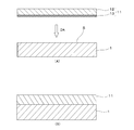
- FIG. 1A shows a state in which a surface protection tape is attached to the surface of a semiconductor wafer
- FIG. 1B shows a semiconductor wafer in which a surface protection tape is attached.
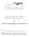
- FIG. 2(A) shows a thinning treatment by backside grinding of a semiconductor wafer
- FIG. 2(B) shows the thinned semiconductor wafer on which the ultraviolet curable adhesive tape for semiconductor wafer processing of the present invention is applied.
- FIG. 2C shows a state in which the semiconductor wafer is fixed to the ring frame.
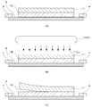
- FIG. 3A shows a state in which the surface protection tape is attached to the front surface of the semiconductor wafer and the ultraviolet curable adhesive tape for semiconductor wafer processing of the present invention is attached to the back surface of the semiconductor wafer.
- FIG. 3B shows a state in which ultraviolet rays from an LED lamp as a light source are irradiated from the surface side to which the surface protection tape is attached, and
- FIG. 3C shows a state in which the surface protection tape is peeled off.
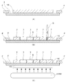
- FIG. 4(A) shows a state after the surface protection tape is peeled off from the semiconductor wafer
- FIG. 4(B) shows a step of dividing into individual chips by a dicing blade and dividing into individual pieces.
- FIG. 4(C) shows a state in which ultraviolet rays are radiated from the side to which the ultraviolet-curable adhesive tape for semiconductor wafer processing of the present invention is attached by a second ultraviolet ray irradiation device using a high pressure mercury lamp as a light source. Indicates.
- the ultraviolet curable adhesive tape for semiconductor wafer processing of the present invention (hereinafter, also referred to as “adhesive tape of the present invention”) 2 is a base film 3 and an ultraviolet curable adhesive layer provided on the base film 3. 4 is a tape having at least 4.
- a release liner also referred to as a separator
- the release liner is peeled off to expose the pressure-sensitive adhesive layer 4 for use.
- the pressure-sensitive adhesive tape 2 of the present invention is a pressure-sensitive adhesive tape in which the value of the adhesive force measured by the 90° peeling test method for SUS304 (stainless steel) based on JIS Z 0237 satisfies both the following (1) and (2). ..
- the adhesive tape of the present invention which has been aged for a long period of time or the like, means the adhesive force in a state of being stored in a state where ultraviolet curing does not occur due to light shielding or the like.
- adhesive strength after ultraviolet irradiation means that after the ultraviolet ray irradiating device using each light source lamp irradiates the unused adhesive tape of the present invention with ultraviolet rays having an integrated light amount of 500 mJ/cm 2. Means the adhesive strength of.
- the specific method for measuring the adhesive force is as described in the section of Examples.
- the above [adhesive strength before UV irradiation] (A 0 ) is preferably 1 N/25 mm to 10 N/25 mm from the viewpoint that the adhesive tape of the present invention before UV irradiation has sufficient adhesiveness to a semiconductor wafer, It is more preferably 1 N/25 mm to 5 N/25 mm.
- a LED / A 0 in the above (1) is preferably 0.60 or more, more preferably 0.70 or more.
- the upper limit of A LED /A 0 in (1) above is not particularly limited, but is preferably 1.30 or less, more preferably 1.20 or less, further preferably 1.10 or less, and 1.00 or less. Particularly preferred.
- a HPM /A 0 in (2) above is preferably 0.40 or less, more preferably 0.30 or less, and further preferably 0.20 or less.
- the lower limit of A HPM /A 0 in (2) above is not particularly limited, but is preferably 0.05 or more, more preferably 0.10 or more.
- Adhesive strength after UV irradiation (hereinafter also abbreviated as “A LED /A HPM ”) is preferably 0.2 to 200, and more preferably 2.0 to 100.
- the adhesive tape 2 of the present invention has a wavelength of 365 nm when A LED /A 0 and A HPM /A 0, which are the ratios of the adhesive strength values before and after irradiation with ultraviolet rays, satisfy the above (1) and (2).
- UV irradiation using an LED lamp (also simply referred to as “LED lamp” in the present specification) as a light source can suppress a decrease in adhesive strength, and ultraviolet irradiation using a high-pressure mercury lamp as a light source can provide sufficient adhesive strength. Can be lowered.
- the adhesive tape 2 of the present invention when used as a dicing tape in a semiconductor wafer processing step, by using an LED lamp as a light source for irradiating the surface protection tape with ultraviolet rays, the surface protection tape is irradiated with ultraviolet rays. With this, it is possible to suppress the decrease in adhesive strength, and it is possible to suppress chip flying during dicing even when the ultraviolet rays of the LED lamp enter the adhesive tape 2 (dicing tape) of the present invention.
- the adhesive tape 2 of the present invention can sufficiently reduce the adhesive force of the adhesive tape 2 of the present invention by irradiation with ultraviolet rays using a high-pressure mercury lamp as a light source, and can exhibit excellent pickup properties.
- the substrate film 3 in the present invention is not particularly limited, and a known resin such as plastic can be used.
- a thermoplastic plastic film is usually used as a base film forming a tape for semiconductor wafer dicing (hereinafter referred to as "dicing tape").
- the resin (material) constituting the base film 3 for example, polyolefin such as polyethylene, polypropylene, ethylene-propylene copolymer and polybutene, styrene-hydrogenated isoprene-styrene block copolymer, styrene-isoprene-styrene copolymer
- Thermoplastic elastomers such as polymer, styrene-hydrogenated butadiene-styrene copolymer and styrene-hydrogenated isoprene/butadiene-styrene copolymer, ethylene-vinyl acetate copolymer, ethylene-(meth)acrylic acid copolymer, Ethylene copolymers such as ethylene-(meth)acrylic acid ester copolymers and ethylene-(meth)acrylic acid metal salt-based ionomers, polyethylene terephthalate, polybuty
- one kind of the resin constitutional unit, (meth)acrylic acid, (meth)acrylic acid ester and (meth)acrylic acid metal salt may be contained in the ethylene copolymer. Two or more kinds may be contained.
- the metal salt of the ethylene-(meth)acrylic acid metal salt-based ionomer is preferably a divalent or higher valent metal salt, and examples thereof include a Zn 2+ metal salt.
- the resin forming the base film 3 one kind or two or more kinds of resins can be used.
- the base film 3 may have a single-layer structure or a multi-layer body in which two or more layers are laminated. The resin forming the base film 3 can be appropriately selected according to the adhesiveness to the pressure-sensitive adhesive layer 4.
- the base film 3 a commercially available film may be used, or a film formed by a conventional method such as a casting method, a T-die method, an inflation method and a calender method may be used.
- the thickness of the base film 3 is not particularly limited, and can be set to the thickness of the base film in an ordinary dicing tape. Generally, it is preferably 30 to 200 ⁇ m, more preferably 50 to 150 ⁇ m.
- the surface of the base film 3 in contact with the pressure-sensitive adhesive layer 4 may be subjected to any surface treatment such as corona treatment or primer treatment in order to improve the adhesion.
- the pressure-sensitive adhesive constituting the pressure-sensitive adhesive layer 4 is an ultraviolet-curable pressure-sensitive adhesive (hereinafter, simply referred to as “pressure-sensitive adhesive”) capable of satisfying the ratio of pressure-sensitive adhesive strength before and after ultraviolet irradiation specified in (1) and (2) above. (Also referred to as “.”) is not particularly limited. Specifically, the pressure-sensitive adhesive layer 4 containing the above-mentioned UV-curable pressure-sensitive adhesive does not cure much when irradiated with UV rays from an LED lamp having a wavelength of 365 nm as a light source, and the adhesive force is less likely to decrease due to this UV irradiation. ..
- the ultraviolet irradiation using a high pressure mercury lamp as a light source causes curing to proceed, the adhesive force can be sufficiently reduced, and peeling from the semiconductor wafer (semiconductor chip) becomes easy. That is, when a high-pressure mercury lamp is used as a light source, light with a wide wavelength distribution including wavelengths such as 254 nm, 313 nm, 365 nm, 405 nm, and 436 nm can be emitted. In comparison, the curing reaction can be made more efficient.
- the pressure-sensitive adhesive layer 4 is an ultraviolet curable layer having different curing reactivity depending on the wavelength range (wavelength distribution) of the ultraviolet rays to be irradiated.
- the polymer contained in the pressure-sensitive adhesive also referred to as “base polymer” in the present specification
- a (meth)acrylic polymer is preferable.
- the content of the base polymer contained in the pressure-sensitive adhesive layer 4 is preferably 50 to 95% by mass, more preferably 70 to 95% by mass.
- the UV-curable pressure-sensitive adhesive may be any pressure-sensitive adhesive that has different curing reactivity depending on the wavelength range of the ultraviolet rays to be irradiated.
- curing by ultraviolet irradiation using a high-pressure mercury lamp as a light source may be one that utilizes the property of three-dimensional reticulation, and is roughly classified into 1) a side chain and an ultraviolet polymerizable carbon-carbon double bond ( An adhesive containing a base polymer having an ethylenic double bond), and 2) at least two UV-polymerizable carbons in the molecule, in contrast to an ordinary rubber-based or (meth)acrylic pressure-sensitive base polymer. It is classified as a pressure-sensitive adhesive containing a low molecular weight compound having a carbon double bond (ethylenic double bond) (hereinafter referred to as an ultraviolet polymerizable low molecular weight compound).
- the pressure-sensitive adhesive tape 2 of the present invention contains a low-molecular weight compound (having a molecular weight of about 1000 or less), the low-molecular-weight compound is changed to a low-molecular-weight compound when the irradiation of ultraviolet rays or picking up is long after the pressure-sensitive adhesive tape is attached to a semiconductor wafer.
- a phenomenon in which the adhesion is increased and the peeling between the adhesive tape and the semiconductor chip at the time of pickup becomes heavy due to the transition to the interface between the semiconductor wafer or the semiconductor chip and the semiconductor wafer.
- the UV-curable pressure-sensitive adhesive is preferably a pressure-sensitive adhesive containing the base polymer having a UV-polymerizable carbon-carbon double bond (ethylenic double bond) in the side chain of the above 1).
- the pressure-sensitive adhesive of 1) may contain a low molecular weight compound, but it is more preferable that the content is such that the phenomenon that the peeling becomes heavy is not observed. It should be noted that the inclusion of a photopolymerization initiator and a curing agent described later is not limited.
- the pressure-sensitive adhesive forming the pressure-sensitive adhesive layer 4 contains a base polymer having a UV-polymerizable carbon-carbon double bond in its side chain
- the pressure-sensitive adhesive layer 4 contains a UV-polymerizable carbon-carbon double bond in its side chain. It is preferable to include a (meth)acrylic polymer having The content of the (meth)acrylic polymer having the UV-polymerizable carbon-carbon double bond in the side chain in the pressure-sensitive adhesive layer 4 is preferably 50% by mass or more, more preferably 80% by mass or more.
- the (meth)acrylic polymer may have a functional group such as an epoxy group or a carboxy group in addition to the UV-polymerizable carbon-carbon double bond (ethylenic double bond) in the side chain.
- the (meth)acrylic polymer having a UV-polymerizable carbon-carbon double bond in its side chain a (meth)acrylic polymer in which at least one kind of constitutional unit of the polymer has an ethylenic carbon-carbon double bond is preferable.
- the (meth)acrylic polymer may be produced by any method, and can be produced by a conventional method.
- a (meth)acrylic polymer having a functional group ( ⁇ ) in the side chain and an ultraviolet-polymerizable carbon-carbon double bond such as a (meth)acryloyl group and the side of this (meth)acrylic polymer Those obtained by reacting a compound having a functional group ( ⁇ ) capable of reacting with the functional group ( ⁇ ) of the chain are preferable.
- the group having a UV-polymerizable carbon-carbon double bond may be any group as long as it has a non-aromatic ethylenic double bond, but a (meth)acryloyl group, a (meth)acryloyloxy group, A (meth)acryloylamino group, an allyl group, a 1-propenyl group, a vinyl group (including styrene or a substituted styrene) are preferable, and a (meth)acryloyl group or a (meth)acryloyloxy group is more preferable.
- the other functional group when one of the functional group ( ⁇ ) and the functional group ( ⁇ ) is a carboxy group, a hydroxyl group, an amino group, a mercapto group, or a cyclic acid anhydride group, the other functional group is , An epoxy group and an isocyanate group, and when one functional group is a cyclic acid anhydride group, the other functional group includes a carboxy group, a hydroxyl group, an amino group and a mercapto group.
- the other functional group may be an epoxy group.
- the (meth)acrylic polymer having a functional group ( ⁇ ) in the side chain is a (meth)acrylic monomer having a functional group ( ⁇ ), preferably a (meth)acrylic acid ester [(particularly, the functional group ( ⁇ ) in the alcohol part is And the like] are used as the monomer component.
- the (meth)acrylic polymer having a functional group ( ⁇ ) on its side chain is preferably a copolymer.
- the copolymerization component with the (meth)acrylic monomer having a functional group ( ⁇ ) in the side chain is a (meth)acrylic acid alkyl ester, especially the functional group ( ⁇ ) in the alcohol part or the UV-polymerizable carbon-carbon.
- a (meth)acrylic acid alkyl ester in which a group having a double bond is not substituted is preferable.
- Examples of the (meth)acrylic acid ester include methyl acrylate, ethyl acrylate, n-propyl acrylate, n-butyl acrylate, isobutyl acrylate, n-pentyl acrylate, n-hexyl acrylate, n-octyl acrylate, isooctyl acrylate, 2-ethylhexyl acrylate, dodecyl acrylate, decyl acrylate hexyl acrylate, and their corresponding methacrylates.
- the (meth)acrylic acid ester may be one type or two or more types, but it is preferable to use the alcohol part having a carbon number of 5 or less and the carbon number of 6 to 12 in combination.
- the glass transition point (Tg) becomes lower as a monomer having a larger number of carbon atoms in the alcohol portion is used, so that a desired glass transition point can be obtained.
- a low molecular weight compound having a carbon-carbon double bond such as vinyl acetate, styrene and acrylonitrile for the purpose of improving compatibility and various performances.
- these monomer components The content of is preferably within the range of 5% by mass or less.
- Examples of the (meth)acrylic monomer having a functional group ( ⁇ ) include acrylic acid, methacrylic acid, cinnamic acid, itaconic acid, fumaric acid, phthalic acid, 2-hydroxyalkyl acrylates, 2-hydroxyalkyl methacrylates, glycol mono.
- Acrylates glycol monomethacrylates, N-methylol acrylamide, N-methylol methacrylamide, allyl alcohol, N-alkylaminoethyl acrylates, N-alkylaminoethyl methacrylates, acrylamides, methacrylamides, maleic anhydride, anhydrous Itaconic acid, fumaric anhydride, phthalic anhydride, glycidyl acrylate, glycidyl methacrylate, allyl glycidyl ether, a monomer having a part of the isocyanate groups of a polyisocyanate compound as a hydroxyl group or a carboxy group and a UV-polymerizable carbon-carbon double bond Examples include those made into urethane.
- acrylic acid, methacrylic acid, 2-hydroxyalkyl acrylates, 2-hydroxyalkyl methacrylates, glycidyl acrylate or glycidyl methacrylate are preferable, and acrylic acid, methacrylic acid, 2-hydroxyalkyl acrylates or 2-hydroxyalkyl methacrylate are preferred. More preferred are 2-hydroxyalkyl acrylates and 2-hydroxyalkyl methacrylates.
- the functional group ( ⁇ ) in the compound having the UV-polymerizable carbon-carbon double bond and the functional group ( ⁇ ) is preferably an isocyanate group, for example, having an isocyanate (—N ⁇ C ⁇ O) group in the alcohol part ( Examples thereof include (meth)acrylic acid ester, and among them, (meth)acrylic acid alkyl ester substituted with an isocyanate (—N ⁇ C ⁇ O) group is preferable. Examples of such a monomer include 2-isocyanatoethyl methacrylate and 2-isocyanatoethyl acrylate. Further, when the functional group ( ⁇ ) is other than an isocyanate group, preferable compounds include the compounds exemplified as the (meth)acrylic monomer having the functional group ( ⁇ ).
- the polymer By reacting a compound having a UV-polymerizable carbon-carbon double bond and a functional group ( ⁇ ) with a (meth)acrylic polymer having a functional group ( ⁇ ) in a side chain, the polymer can be UV-polymerizable carbon-carbon.
- a double bond can be incorporated to form a UV-curable pressure-sensitive adhesive layer.
- ketone-based, ester-based, alcohol-based, aromatic-based ones can be used, among which toluene, ethyl acetate.
- a good solvent of (meth)acrylic polymer such as isopropyl alcohol, benzene methyl cellosolve, ethyl cellosolve, acetone, and methyl ethyl ketone, and a solvent having a boiling point of 60 to 120° C. is preferable.
- a radical generator such as an azobis type such as ⁇ , ⁇ ′-azobisisobutyronitrile or an organic peroxide type such as benzoyl peroxide is usually used.
- a catalyst and a polymerization inhibitor can be used in combination, if necessary, and a (meth)acrylic polymer having a desired molecular weight can be obtained by adjusting the polymerization temperature and the polymerization time.
- a solvent such as mercaptan or carbon tetrachloride. Note that this reaction is not limited to solution polymerization, and other methods such as bulk polymerization and suspension polymerization may be used.
- the mass average molecular weight (Mw) of the base polymer having a UV-polymerizable carbon-carbon double bond in its side chain [preferably (meth)acrylic polymer] is preferably about 200,000 to 1,000,000.
- the adhesive layer 4 does not become brittle and has flexibility even when irradiated with ultraviolet rays, and therefore adhesive residue is less likely to occur on the semiconductor chip surface during peeling.
- the mass average molecular weight is 200,000 or more, the cohesive force before irradiation with ultraviolet rays is not too small and has sufficient adhesive force, so that the semiconductor chip can be sufficiently held during dicing and chip fly hardly occurs. ..
- curing after ultraviolet irradiation is sufficient, and adhesive residue hardly occurs on the semiconductor chip surface during peeling.
- the mass average molecular weight in the present invention is a polystyrene equivalent mass average molecular weight.
- the amount of the UV-polymerizable carbon-carbon double bond introduced into the base polymer having the UV-polymerizable carbon-carbon double bond in the side chain is preferably 0.8 to 1.8 meq/g, and 0.8 to 1 More preferably, it is 0.5 meq/g.
- the introduction amount of the UV-polymerizable carbon-carbon double bond is within the above range, the curing reaction is sufficiently advanced by the UV irradiation from the high-pressure mercury lamp as a light source, and moreover, there is sufficient fluidity, and thus the adhesive residue is left. Will be reduced.
- the glass transition point of the base polymer having a UV-polymerizable carbon-carbon double bond in its side chain is preferably -70 to -35°C, more preferably -70 to -40°C.
- the glass transition temperature of the base polymer used for the pressure-sensitive adhesive layer 4 is a value measured by a differential scanning calorimeter (DSC) at a temperature rising rate of 0.1° C./min.
- DSC differential scanning calorimeter
- the glass transition temperature is the extrapolated glass transition start temperature of JIS K 7121 “Plastic transition temperature measurement method”.
- the acid value of the base polymer having a UV-polymerizable carbon-carbon double bond in the side chain [mg of potassium hydroxide necessary to neutralize free fatty acid present in 1 g of the base polymer] is 0.5 to 30 is preferable, and 1 to 20 is more preferable.
- Hydroxyl value of base polymer having UV-polymerizable carbon-carbon double bond in side chain [mg of potassium hydroxide required to neutralize acetic acid bound to hydroxyl group when 1 g of base polymer is acetylated ] Is preferably 5 to 100, more preferably 10 to 80. By doing so, the adhesive residue prevention effect at the time of peeling the adhesive tape of the present invention is further excellent.
- the acid value and the hydroxyl value are adjusted by using a (meth)acrylic polymer having a functional group ( ⁇ ) in the side chain and an ultraviolet-polymerizable carbon-carbon double bond, and A desired compound can be prepared by leaving an unreacted functional group at the stage of reacting a compound having a functional group ( ⁇ ) capable of reacting with the functional group ( ⁇ ) of the side chain.
- the pressure-sensitive adhesive containing the base polymer having a UV-polymerizable carbon-carbon double bond in its side chain preferably contains a curing agent.
- the curing agent is used to react with the functional groups of the base polymer to adjust the adhesive force and cohesive force.
- the curing agent preferably includes polyisocyanates, melamine-formaldehyde resin and epoxy resin. Among these, polyisocyanates are more preferable in the present invention.
- the polyisocyanate is not particularly limited and includes, for example, 4,4′-diphenylmethane diisocyanate, tolylene diisocyanate, xylylene diisocyanate, 4,4′-diphenyl ether diisocyanate, 4,4′-[2,2-bis(4 -Phenoxyphenyl)propane] diisocyanate and other aromatic isocyanates, hexamethylene diisocyanate, 2,2,4-trimethyl-hexamethylene diisocyanate, isophorone diisocyanate, 4,4'-dicyclohexylmethane diisocyanate, 2,4'-dicyclohexylmethane diisocyanate , Lysine diisocyanate, lysine triisocyanate and the like.
- Coronate L (trade name, manufactured by Nippon Polyurethane Co., Ltd.) or the like can be used.
- melamine/formaldehyde resin examples include Nicalac MX-45 (manufactured by Sanwa Chemical Co., Ltd., product name) and Melan (manufactured by Hitachi Chemical Co., Ltd., product name).
- TETRAD-X (trade name, manufactured by Mitsubishi Chemical Corporation) or the like can be used.
- the base polymer After the pressure-sensitive adhesive is applied, the base polymer forms a crosslinked structure with the curing agent, whereby the cohesive force of the pressure-sensitive adhesive can be improved.
- the above curing agent is already in a state of reacting with the base polymer in the adhesive layer 4 of the unused adhesive tape.
- the term "base polymer component" does not include a curing agent component. That is, in the state where the base polymer and the curing agent have reacted, the structural portion excluding the curing agent component is referred to as the base polymer component. However, all the curing agents contained in the pressure-sensitive adhesive layer 4 may be reacted, or some of them may be reacted.
- the content of the curing agent component is preferably 0.1 to 10 parts by mass and more preferably 1 to 10 parts by mass with respect to 100 parts by mass of the base polymer component.
- the content of the curing agent component is at least the above lower limit, the effect of improving the cohesive force becomes sufficient and the adhesive residue of the pressure-sensitive adhesive is suppressed.
- the pressure-sensitive adhesive layer and the surface of the adherend are less likely to shift, and peeling during expansion is suppressed.
- the compounding quantity of a hardening agent is below the said upper limit. The workability is excellent because the curing reaction proceeds without rapidly forming a crosslinked structure during the mixing and application of the pressure-sensitive adhesive. In addition, the flexibility of the pressure-sensitive adhesive is not impaired, and peeling during expansion is suppressed.
- a cross-linking agent can be added in order to add cohesive force to the base polymer of the adhesive.
- the cross-linking agent include metal chelate-based cross-linking agents, aziridine-based cross-linking agents, and amine resins corresponding to the base polymer.
- the pressure-sensitive adhesive may contain various additive components, if desired, as long as the object of the present invention is not impaired.
- photopolymerization initiator When the base polymer having a UV-polymerizable carbon-carbon double bond in its side chain is cured by UV irradiation, it is preferable to incorporate a photopolymerization initiator in the adhesive.
- the photopolymerization initiator is not particularly limited, and commonly used photopolymerization initiators can be widely used.
- isopropyl benzoin ether isobutyl benzoin ether, benzophenone, Michler's ketone, chlorothioxanthone, dodecyl thioxanthone, dimethyl thioxanthone, diethyl thioxanthone, benzyl dimethyl ketal, ⁇ -hydroxycyclohexyl phenyl ketone, 2-hydroxymethyl phenyl propane, etc.
- isopropyl benzoin ether isobutyl benzoin ether
- benzophenone Michler's ketone
- chlorothioxanthone dodecyl thioxanthone
- dimethyl thioxanthone dimethyl thioxanthone
- diethyl thioxanthone diethyl thioxanthone
- benzyl dimethyl ketal ⁇ -hydroxycyclohexyl phenyl ketone
- the content of the photopolymerization initiator in the pressure-sensitive adhesive layer 4 is 0.1 to 100 parts by mass of the base polymer component.
- the amount is preferably 3.0 parts by mass, more preferably 0.1 to 1.5 parts by mass, still more preferably 0.1 to 1.0 parts by mass.
- the content of the photopolymerization initiator is less than or equal to the above upper limit, between the curing reactivity by ultraviolet irradiation with an LED lamp having a wavelength of 365 nm as a light source and the curing reactivity by ultraviolet irradiation with a high pressure mercury lamp as a light source, It is possible to have a desired difference.
- the content of the photopolymerization initiator is at least the above lower limit value, the curing reaction sufficiently progresses and cures upon irradiation with ultraviolet rays from a high pressure mercury lamp as a light source, and the adhesive tape 2 of the present invention and the adherend are adhered to each other. The peelability can be further improved.
- UV absorber An ultraviolet absorber may be added to the pressure-sensitive adhesive tape 2 of the present invention from the viewpoint of enhancing the absorption in a predetermined wavelength range and controlling the curing reactivity when a predetermined light source is used.
- the ultraviolet absorber preferably contains at least one kind of ultraviolet absorber having a triazine skeleton, a benzophenone skeleton, a benzotriazole skeleton or a benzoate skeleton.
- the compound having a triazine skeleton include 2,4-bis[2-hydroxy-4-butoxyphenyl]-6-(2,4-dibutoxyphenyl)-1,3,5-triazine and 2,4- Bis(2,4-dimethylphenyl)-6-(2-hydroxy-4-n-octyloxyphenyl)-1,3,5-triazine, 2-(2,4-dihydroxyphenyl)-4,6-bis (2,4-Dimethylphenyl)-1,3,5-triazine, 2-(2,4-dihydroxyphenyl)-4,6-diphenyl-1,3,5-triazine, 2-(2-hydroxy-4) -Methoxyphenyl)-4,6-diphenyl-1,3,5-triazine
- Examples of the compound having a benzophenone skeleton include 2,4-dihydroxybenzophenone, 2,2'-dihydroxy-4,4'-dimethoxybenzophenone, 2-hydroxy-4-methoxybenzophenone, 2-hydroxy-4-n-octyl Roxybenzophenone and 2,2′,4,4′-tetrahydroxybenzophenone can be mentioned.
- Examples of the compound having a benzotriazole skeleton include 2-(2-hydroxy-5-t-butylphenyl)-2H-benzotriazole and 2-(2H-benzotriazol-2-yl)-4,6-bis( 1-methyl-1-phenylethyl)phenol, 2-(2H-benzotriazol-2-yl)-6-(1-methyl-1-phenylethyl)-4-(1,1,3,3-tetramethyl Butyl)phenol.
- Examples of the compound having a benzoate skeleton include 2,4-di-t-butylphenyl-3,5-di-t-butyl-4-hydroxybenzoate and 2,4-di-t-butylphenyl-4′- Hydroxy-3',5'-di-t-butyl benzoate may be mentioned.
- UV absorber As the above-mentioned ultraviolet absorber, a commercially available one may be used. For example, all of them are trade names under the trade name of Adeka Stab LA series (LA-24, LA-29, LA-31, LA-32). , LA-36, LA-F70, 1413), BASF TINUVIN P, TINUVIN 234, TINUVIN 326, TINUVIN 329, TINUVIN 213, TINUVIN 571, TINUVIN 1577ED, CHIMASSORB 81, TINUVIN 120, etc.
- Adeka Stab LA series LA-24, LA-29, LA-31, LA-32).
- LA-36 LA-F70, 1413
- BASF TINUVIN P TINUVIN 234, TINUVIN 326, TINUVIN 329, TINUVIN 213, TINUVIN 571, TINUVIN 1577ED, CHIMASSORB 81, TINUVIN 120, etc.
- the ultraviolet absorbers may be used alone or in combination of two or more.
- the addition amount of the ultraviolet absorber can be adjusted according to the curing reactivity with respect to a desired wavelength range. For example, 0.1 to 10.0 parts by mass is preferable, 0.1 to 5.0 parts by mass is more preferable, and 0.1 to 1.0 parts by mass is more preferable, relative to 100 parts by mass of the base polymer.
- the pressure-sensitive adhesive may contain a solvent in terms of coatability when the pressure-sensitive adhesive is applied to a release liner to form a uniform pressure-sensitive adhesive.
- the solvent is not particularly limited, and may be a solvent commonly used as an adhesive in a tape for processing a semiconductor wafer.
- the thickness of the adhesive layer 4 is not particularly limited and may be set appropriately, but in the present invention, it is preferably 5 to 30 ⁇ m.
- the pressure-sensitive adhesive tape 2 of the present invention protects the pressure-sensitive adhesive layer 4 before use, so that a release film is preferably temporarily adhered to the upper surface of the pressure-sensitive adhesive layer 4.
- the method of providing the base film 3 and the method of providing the pressure-sensitive adhesive layer 4 on the base film 3 are not particularly limited, and may be appropriately selected from known methods. An example is described below, but the invention is not limited to the example below.
- An adhesive is applied on the release liner to form the adhesive layer 4 having a desired thickness.
- the pressure-sensitive adhesive tape 4 of the present invention can be produced by bonding the pressure-sensitive adhesive layer 4 and the base film 3 (resin forming the base film into a film).
- the pressure-sensitive adhesive tape of the present invention is also preferably stored under light-shielding conditions after production.
- the pressure-sensitive adhesive tape 2 of the present invention can suppress the decrease in the adhesive force by irradiation with ultraviolet rays using an LED as a light source, and can sufficiently reduce the adhesive force by irradiation with ultraviolet rays using a high pressure mercury lamp as a light source. Therefore, by using the adhesive tape 2 of the present invention as a dicing tape (fixing tape) in the production of semiconductor chips, it is possible to suppress the warp of the thin film wafer due to the irradiation of the surface protection tape with ultraviolet rays, and at the time of dicing. It is possible to achieve both suppression of chip fly and excellent pick-up property thereafter.
- the adhesive tape 2 of the present invention and the UV-curable surface protection tape are attached to a semiconductor wafer, respectively, and the UV-curable surface protection tape is cured by UV irradiation using an LED lamp having a wavelength of 365 nm as a light source.
- the UV-curable surface protection tape can be cured and peeled from the semiconductor wafer while sufficiently suppressing the decrease in the adhesive strength of the adhesive tape 2 of the present invention.
- the irradiation conditions of each ultraviolet ray can be appropriately adjusted to obtain a desired adhesive force.
- the method of manufacturing a semiconductor chip of the present invention is a method of obtaining a semiconductor chip using the adhesive tape 2 of the present invention.
- an ultraviolet-curable surface protection tape (hereinafter, also simply referred to as “surface protection tape”) is attached to the pattern surface side of a semiconductor wafer having a pattern surface on the surface, while protecting the pattern surface in that state.
- the back surface of the semiconductor wafer is ground.
- the adhesive tape 2 of the present invention is attached to the back surface of the semiconductor wafer, and is supported and fixed to the ring frame.
- the surface protection tape is peeled off to expose the pattern surface on the surface of the semiconductor wafer.
- the semiconductor wafer is cut from the pattern surface side of the semiconductor wafer by using a dicing device, and individual semiconductor chips are diced into individual chips (dicing), whereby a target semiconductor chip can be obtained.
- the dicing method is not particularly limited, and a usual method can be adopted. Of these, dicing using a dicing blade is preferable.
- the adhesiveness of the adhesive tape 2 is further reduced by irradiating the adhesive tape 2 of the present invention with ultraviolet rays from the second ultraviolet irradiation device.
- the first ultraviolet irradiation device is preferably, for example, an ultraviolet irradiation device using an LED lamp having a wavelength of 365 nm as a light source.
- the second ultraviolet irradiation device is preferably, for example, an ultraviolet irradiation device using a high pressure mercury lamp as a light source.
- the conditions of the ultraviolet irradiation by the first ultraviolet irradiation device and the ultraviolet irradiation by the second ultraviolet irradiation device may be appropriately adjusted according to the surface protection tape to be used and the curing reactivity of the adhesive tape 2 of the present invention with respect to the light source. it can. Irradiation conditions are not particularly limited.
- ultraviolet irradiation using an LED lamp with a wavelength of 365 nm as a light source preferably has an irradiation intensity of 30 mW/cm 2 to 50 mW/cm 2 , and an integrated light amount of 200 mJ/cm 2 to 1000 mJ. /Cm 2 is preferable, and the ultraviolet irradiation using a high pressure mercury lamp as a light source preferably has an irradiation intensity of 40 mW/cm 2 to 80 mW/cm 2 , and an integrated light amount of ultraviolet rays (wavelength 250 nm to 450 nm). Is preferably 200 mJ/cm 2 to 1000 mJ/cm 2 .
- the type of the high pressure mercury lamp is not particularly limited, and a commonly used high pressure mercury lamp can be used.
- UV-curable surface protection tape it is possible to use an UV-curable surface protection tape which is usually used for protecting the pattern surface of a semiconductor wafer in the manufacturing process of semiconductor chips. Specifically, it is not particularly limited as long as it has at least a base film and an ultraviolet-curable pressure-sensitive adhesive layer provided on the base film.
- a preferable mode is one in which a film-like semiconductor encapsulant is provided as NCF (non conductive film, non-conductive film) on the surface of the adhesive layer opposite to the side having the base film.
- NCF non conductive film, non-conductive film
- peeling off the surface protection tape from the semiconductor wafer means that the film-like semiconductor encapsulant is left on the semiconductor wafer and is adhered to the base film. It means peeling together with the agent layer.
- FIGS. 1-10 A preferred embodiment of the semiconductor chip manufacturing method of the present invention (hereinafter, also simply referred to as “manufacturing method to which the present invention is applied”) will be described below with reference to FIGS.
- the following embodiments are not limited to the following embodiments unless otherwise specified, unless otherwise specified.
- the form shown in each drawing is a schematic cross-sectional view for facilitating the understanding of the present invention, and the size, thickness, or relative size relationship of each member is changed for convenience of description. However, it does not show the actual relationship as it is. Further, other than matters specified in the present invention, the external shape and shape shown in these drawings are not limited.
- the semiconductor wafer 1 has a pattern surface on the surface S of which semiconductor device circuits and the like are formed (see FIG. 1A).
- the pattern surface is a surface on which circuits of a semiconductor element are formed and has streets in a plan view.
- a surface protection tape 11 having a UV curable pressure sensitive adhesive layer 13 provided on a base film 12 is adhered to obtain a semiconductor wafer 1 whose pattern surface is covered with the surface protection tape 11 (separation diagram). 1 (B)).
- the base film 12 and the adhesive layer 13 are shown together as a surface protection tape 11.
- the arrow DA in FIG. 1A shows the direction in which the surface protection tape 11 is attached to the semiconductor wafer 1.
- the back surface of the semiconductor wafer 1 is ground by the wafer grinding machine M1 to reduce the thickness of the semiconductor wafer 1 (see FIG. 2(A)).
- the adhesive tape 2 of the present invention is attached to the back surface B of the semiconductor wafer 1B whose back surface is ground (see FIG. 2B), and the adhesive tape 2 of the present invention is supported and fixed to the ring frame F. (See FIG. 2(C) and FIG. 3(A)).
- arrow DB in FIG. 2A shows the rotation direction of the grinding wheel in the wafer grinding apparatus M1
- arrow DC in FIG. 2B shows the adhesion of the present invention to the back surface B of the semiconductor wafer 1. The direction in which the tape 2 is attached is shown.
- ultraviolet rays UV are obtained by using a first ultraviolet ray irradiation device UVS1 having an LED lamp having a wavelength of 365 nm as a light source. (Indicated by the arrow in the note) (see Fig. 3(B)).
- UVS1 ultraviolet ray irradiation device having an LED lamp having a wavelength of 365 nm as a light source.
- the pressure-sensitive adhesive layer 13 of the surface protection tape 11 is cured to reduce the adhesive strength, and then the surface protection tape 11 is peeled off (see FIG. 3C), and the semiconductor wafer surface is exposed. (See FIG. 4A for minutes).
- the pattern surface side (the surface S side) of the semiconductor wafer 1 is processed by the dicing blade D, the wafer is cut, and the individual chips 7 are divided into individual pieces (division FIG. 4B). reference).
- ultraviolet rays UV shown by an arrow in FIG. 4C
- UVS2 using a high-pressure mercury lamp as a light source
- minute diagram 4C minute diagram 4C.
- the pressure-sensitive adhesive layer 4 of the pressure-sensitive adhesive tape 2 of the present invention is cured to reduce the pressure-sensitive adhesive force.
- the individual chips 7 are picked up by a pick-up device by a push-up by a pin and suction by a collet (not shown).
- UV irradiation using the second UV irradiation device UVS2 using a high-pressure mercury lamp as a light source which is shown in FIG. It is also preferable to provide a certain distance between the chips 7 that have been embodied.
- a tape having expandability is used as the adhesive tape 2 of the present invention. Conditions such as an expanding speed and an expanding amount can be appropriately adjusted, and examples thereof include an embodiment using an expander.
- an ultraviolet curable surface protection tape is attached to one surface (for example, a pattern surface) of the semiconductor wafer 1, and the adhesive tape 2 of the present invention is attached to the other surface of the semiconductor wafer 1.
- the surface protection tape 11 preferably the pressure-sensitive adhesive layer of the surface protection tape
- the ultraviolet irradiation is preferably ultraviolet irradiation using an LED lamp with a wavelength of 365 nm as a light source.
- the method of using the pressure-sensitive adhesive tape 2 of the present invention preferably has a step of peeling the surface protection tape 11 from the semiconductor wafer after the above-mentioned ultraviolet irradiation, and further, after the step of peeling the surface protection tape 11, the present invention It is more preferable to have a step of irradiating the adhesive tape 2 with ultraviolet rays. By this irradiation of ultraviolet rays, the pressure-sensitive adhesive layer in the pressure-sensitive adhesive tape 2 of the present invention is cured to reduce the adhesive strength.
- the ultraviolet irradiation is preferably ultraviolet irradiation using a high pressure mercury lamp as a light source.
- each UV irradiation can be appropriately adjusted according to the reactivity of the surface protection tape 11 and the adhesive tape 2 of the present invention to the light source, as long as the effects of the present invention are not impaired.
- Irradiation conditions are not particularly limited, but for example, the description of the conditions of ultraviolet irradiation in the method of manufacturing the semiconductor chip 1 of the present invention described above can be preferably applied.
- the method of using the adhesive tape of the present invention can be preferably applied to the method of manufacturing the semiconductor chip 1 described above.
- the method of using the adhesive tape 2 of the present invention is a TSV (through silicon electrode, Through-) using a film-like semiconductor encapsulant-integrated surface protection tape (hereinafter also referred to as “integrated surface protection tape”). It can be preferably used also in the processing step of the middle layer of the Silicon Via) wafer.
- the processing step of the middle layer of the TSV wafer includes the following steps. First, a via is formed in a state where the support glass is bonded to one surface of the wafer.
- the wafer surface on the opposite side (opposite side) to the surface to which the support glass is attached is back-ground (BG ground) to form bumps on the ground surface.
- BG ground back-ground
- a film-like semiconductor sealant-integrated surface protection tape is attached to the surface from which the support glass has been removed.
- UV irradiation is performed from the integrated surface protection tape side, and the surface protection tape is peeled off to leave only the film-like semiconductor sealing agent on the wafer.
- the above-mentioned "semiconductor wafer having an ultraviolet-curable surface protection tape bonded to one surface of a semiconductor wafer and the adhesive tape of the present invention bonded to the other surface of the semiconductor wafer" is a semiconductor wafer. It is preferable that it occurs in the processing step of.
- Example 1 (1) Preparation of Base Film Ethylene-methacrylic acid-(2-methyl-propyl acrylate) terpolymer-Zn 2+ -ionomer resin, Himilan AM-7316 (trade name, manufactured by Mitsui DuPont Chemical Co., Ltd.) was used to produce a base film 3 having a thickness of 80 ⁇ m. Incidentally, one side of this film was subjected to corona treatment.
- Coronate L (manufactured by Nippon Polyurethane Industry Co., Ltd., trade name, as a curing agent, in the composition of the (meth)acrylic copolymer A, in an amount of 100 parts by mass with respect to the (meth)acrylic copolymer A).
- Isocyanate curing agent and 0.1 part by mass of Irgacure 184 (manufactured by BASF, trade name) as a photopolymerization initiator were mixed to obtain an adhesive A.
- Adhesive Tape The adhesive A was coated on a release liner so that the thickness after drying was 10 ⁇ m to form an adhesive layer 4.
- the formed pressure-sensitive adhesive layer 4 is bonded to the surface side of the base film 3 having a thickness of 80 ⁇ m prepared above, which has been subjected to the corona treatment, and has a total thickness of 90 ⁇ m, which is an ultraviolet-curable pressure-sensitive adhesive tape (adhesive tape) 2 for semiconductor wafer processing.
- an ultraviolet-curable pressure-sensitive adhesive tape (adhesive tape) 2 for semiconductor wafer processing.
- Example 2 In the pressure sensitive adhesive A used in Example 1, the blending amount of Irgacure 184 (manufactured by BASF), which is a photopolymerization initiator, was changed from 0.1 parts by mass to 0.75 parts by mass to obtain a pressure sensitive adhesive B.
- An adhesive tape 2 was produced in the same manner as in Example 1 except that the adhesive B was used instead of the adhesive A.
- Example 3 In the pressure-sensitive adhesive A used in Example 1, the amount of Irgacure 184 (manufactured by BASF), which is a photopolymerization initiator, was changed from 0.1 parts by mass to 1.0 part by mass to obtain a pressure-sensitive adhesive C.
- An adhesive tape 2 was produced in the same manner as in Example 1 except that the adhesive C was used instead of the adhesive A.
- Example 4 In the adhesive A used in Example 1, the compounding amount of Irgacure 184 (manufactured by BASF), which is a photopolymerization initiator, was changed from 0.1 parts by mass to 0.5 parts by mass, and LA-F70 as an ultraviolet absorber was used. (Adeka Co., Ltd., trade name) was mixed in an amount of 0.3 part by mass to obtain an adhesive D. An adhesive tape 2 was produced in the same manner as in Example 1 except that the adhesive D was used instead of the adhesive A.
- Irgacure 184 manufactured by BASF
- LA-F70 as an ultraviolet absorber
- Example 5 In the pressure-sensitive adhesive A used in Example 1, the photopolymerization initiator Irgacure 184 (manufactured by BASF) was changed to the photopolymerization initiator Irgacure 651 (manufactured by BASF, trade name), and the compounding amount was adjusted to 0. The amount was changed from 1 part by mass to 0.3 part by mass, and 0.3 part by mass of LA-F70 (manufactured by ADEKA CORPORATION) was blended as an ultraviolet absorber to obtain a pressure-sensitive adhesive E.
- An adhesive tape 2 was produced in the same manner as in Example 1 except that the adhesive E was used instead of the adhesive A.
- Example 1 In the pressure-sensitive adhesive A used in Example 1, the compounding amount of Irgacure 184 (manufactured by BASF), which is a photopolymerization initiator, was changed from 0.1 parts by mass to 5.0 parts by mass to obtain a pressure-sensitive adhesive F. An adhesive tape was produced in the same manner as in Example 1 except that the adhesive F was used instead of the adhesive A.
- Irgacure 184 manufactured by BASF
- the adhesive strength in the present invention is a value measured by a 90° peeling adhesive strength test method for a stainless test plate based on JIS Z 0237.
- the specific measuring method is as follows. The conditions not described below are based on JIS Z 0237. First, three test pieces having a width of 25 mm and a length of 150 mm were collected from the adhesive tape. These test pieces were adhered to a SUS304 steel plate (stainless steel test plate) with a thickness of 1.5 mm to 2.0 mm specified in JIS G 4305, which was finished with No. 280 water-resistant abrasive paper specified in JIS R 6253. did.
- the adhesive force in the present invention is the arithmetic mean of the adhesive forces of the three test pieces measured by the above method.
- the adhesive force (A LED ) after irradiation with ultraviolet rays using an LED lamp having a wavelength of 365 nm as a light source was measured by the above method.
- the adhesive strength (A HPM ) of the pressure-sensitive adhesive tape, which had been left for 1 hour after being irradiated with ultraviolet rays, after irradiation with ultraviolet rays using a high pressure mercury lamp as a light source was measured by the above method.
- Dicing device DFD-6340 (trade name) manufactured by DISCO Blade: NBC-ZH2050 27HEDD (trade name) manufactured by DISCO Blade rotation speed: 40,000 rpm
- Cutting speed 80mm/sec
- Depth of cut into tape 0.07 mm
- Cutting line 41 cutting lines with a length of 205 mm each length and width
- Cutting water flow rate 2 L/min
- Cutting water temperature 23°C
- the adhesive tapes of Examples 1 to 5 are ultraviolet rays having an integrated light amount of 500 mJ/cm 2 by an ultraviolet ray irradiation device using an LED lamp having a wavelength of 365 nm as a light source with respect to (1) [Adhesive force before ultraviolet ray irradiation] defined in the present invention.
- Adhesive strength after irradiation (A LED /A 0 ) has a value of 0.50 or more, and (2) [Adhesive strength before ultraviolet irradiation] to [ultraviolet irradiation device using high-pressure mercury lamp as light source] Adhesive force after irradiation with ultraviolet light having an integrated light amount of 500 mJ/cm 2 ] (A HPM /A 0 ) has a value of 0.50 or less.
- the ultraviolet irradiation type adhesive tapes of Examples 1 to 5 are used by being bonded to one surface of a semiconductor wafer, even if dicing is performed after ultraviolet irradiation using an LED lamp with a wavelength of 365 nm as a light source, dicing is performed. It turned out that the chip fly at the time can be suppressed. Further, it was found that the chips can be satisfactorily peeled from the ultraviolet irradiation type adhesive tape by irradiating ultraviolet rays from a high pressure mercury lamp as a light source after the dicing and then picking up. That is, it was found that the ultraviolet irradiation type adhesive tapes of Examples 1 to 5 were excellent in both suppressing chip fly and picking up.
- the adhesive tape of Comparative Example 1 satisfies (2) defined in the present invention
- the integrated light amount by the ultraviolet irradiation device using the LED lamp having the wavelength of 365 nm as the light source with respect to the [adhesive strength before ultraviolet irradiation] Adhesive force after irradiation with ultraviolet rays of 500 mJ/cm 2 ] (A LED /A 0 ) is 0.10, which does not satisfy 0.50 or more specified in the present invention.
- the adhesive tape of Comparative Example 2 satisfies (2) defined in the present invention, it has an integrated light amount of 500 mJ/cm 2 by an ultraviolet irradiation device using an LED lamp having a wavelength of 365 nm as a light source with respect to [adhesive force before ultraviolet irradiation].
- Adhesive strength after ultraviolet irradiation] (A LED /A 0 ) is 0.33, which does not satisfy 0.50 or more specified in the present invention.
- the pressure-sensitive adhesive tape of Comparative Example 3 satisfies (1) defined in the present invention, but (2) [Adhesive strength before ultraviolet irradiation] [integrated light amount of 500 mJ/cm 2 by an ultraviolet irradiation device using a high-pressure mercury lamp as a light source] [Adhesive strength after UV irradiation] (A HPM /A 0 ) is 0.57, which does not satisfy 0.50 or less specified in the present invention.
- the adhesive tape of Comparative Example 3 was subjected to dicing after irradiation with ultraviolet rays using an LED lamp as a light source, and then was irradiated with ultraviolet rays using a high-pressure mercury lamp as a light source to pick up all 1238 chips. Remained on the adhesive tape, and the picking up property was not sufficient.
- the adhesive tape of the present invention can be suitably used for processing semiconductor wafers.
- Use of the pressure-sensitive adhesive tape of the present invention which comprises bonding the pressure-sensitive adhesive tape of the present invention and a UV-curable surface protection tape to a semiconductor wafer, respectively, and curing the UV-curable surface protection tape with UV rays from an LED lamp having a wavelength of 365 nm as a light source.
- the UV-curable surface protection tape can be peeled off while suppressing the decrease in the adhesive strength of the adhesive tape of the present invention.
Landscapes
- Chemical & Material Sciences (AREA)
- Organic Chemistry (AREA)
- Adhesives Or Adhesive Processes (AREA)
- Dicing (AREA)
- Adhesive Tapes (AREA)
- Mechanical Treatment Of Semiconductor (AREA)
Abstract
Description
他方で、一度の加工によって製造できる半導体チップの数を増やしてチップの製造効率を向上させる点から、半導体ウェハを大径化する傾向にある。半導体ウェハの薄膜化に加えて大径化の流れは、特に、NAND型やNOR型が存在するフラッシュメモリの分野や、揮発性メモリであるDRAMなどの分野で、顕著な傾向を示している。
現在では、12インチの半導体ウェハを厚さ100μm以下に薄膜研削することが標準となってきている。
また、フリップチップ実装に用いられるバンプ付ウェハについても、薄膜化の要求が高まっている。このバンプ付ウェハは、その表面に大きな凹凸を有しているため薄膜加工が難しく、通常の保護テープを用いて裏面研削を行うとウェハ割れが生じたり、ウェハの厚み精度が悪化したりする。そのため、バンプ付ウェハの研削には特殊な表面保護テープが用いられている(引用文献1参照)。
この、ウェハの反りは、上記表面保護テープとして紫外線硬化型の表面保護テープを用いた場合、特に大きくなる。紫外線硬化型のテープは、紫外線を照射することで表面保護テープ中の粘着剤が硬化反応により硬化収縮するため、非紫外線硬化型のテープに比べて反りが大きくなり、ウェハの破損リスクがより高くなる。
<1>
基材フィルムと、該基材フィルム上に設けられた紫外線硬化型の粘着剤層とを少なくとも有する半導体ウェハ加工用紫外線硬化型粘着テープであって、
JIS Z 0237に基づくSUS304に対する90°引きはがし試験方法により測定される前記粘着テープの粘着力の値が、下記(1)及び(2)を共に満たすことを特徴とする、半導体ウェハ加工用紫外線硬化型粘着テープ。
(1)[波長365nmのLEDランプを光源とする紫外線照射装置による積算光量500mJ/cm2の紫外線照射後の粘着力]/[紫外線照射前の粘着力]≧0.50
(2)[高圧水銀ランプを光源とする紫外線照射装置による積算光量500mJ/cm2の紫外線照射後の粘着力]/[紫外線照射前の粘着力]≦0.50
<2>
前記[紫外線照射前の粘着力]が、1N/25mm~10N/25mmであることを特徴とする、<1>に記載の半導体ウェハ加工用紫外線硬化型粘着テープ。
<3>
前記粘着剤層がベースポリマー成分と光重合開始剤とを含有し、該ベースポリマー成分100質量部に対する光重合開始剤の含有量が0.1~3.0質量部であることを特徴とする、<1>又は<2>に記載の半導体ウェハ加工用紫外線硬化型粘着テープ。
<4>
前記ベースポリマーが側鎖に紫外線重合性炭素-炭素二重結合を有するポリマーであることを特徴とする、<1>~<3>のいずれか1つに記載の半導体ウェハ加工用紫外線硬化型粘着テープ。
<5>
前記粘着剤層が紫外線吸収剤を含有することを特徴とする、<1>~<4>のいずれか1つに記載の半導体ウェハ加工用紫外線硬化型粘着テープ。
<6>
半導体ウェハをダイシングする工程において使用されることを特徴とする、<1>~<5>のいずれか1つに記載の半導体ウェハ加工用紫外線硬化型粘着テープ。
<7>
下記工程(a)~(e)を含むことを特徴とする、半導体チップの製造方法。
〔工程〕
(a)表面にパターン面を有する半導体ウェハの該パターン面側に、紫外線硬化型表面保護テープを貼り合せた状態で、該半導体ウェハの裏面を研削する工程、
(b)前記の研削した半導体ウェハの裏面に<1>~<6>のいずれか1つに記載の半導体ウェハ加工用紫外線硬化型粘着テープを貼り合わせ、リングフレームに支持固定する工程、
(c)前記表面保護テープ側から、第1の紫外線照射装置により紫外線照射を行った後、前記表面保護テープを剥離する工程、
(d)前記半導体ウェハのパターン面側からダイシング装置を用いて、半導体ウェハの切断を行い、個々のチップ単位に個片化する工程、および、
(e)前記粘着テープ側から、第2の紫外線照射装置により紫外線照射を行う工程。
<8>
前記第1の紫外線照射装置が、波長365nmのLEDランプを光源とする紫外線照射装置であることを特徴とする、<7>に記載の半導体チップの製造方法。
<9>
前記第2の紫外線照射装置が、高圧水銀ランプを光源とする紫外線照射装置であることを特徴とする、<7>または<8>に記載の半導体チップの製造方法。
<10>
半導体ウェハの一方の面に紫外線硬化型表面保護テープが貼合され、該半導体ウェハのもう一方の面に<1>~<6>のいずれか1つに記載の半導体ウェハ加工用紫外線硬化型粘着テープが貼合された半導体ウェハに対して、該紫外線硬化型表面保護テープ側から紫外線を照射する工程を含むことを特徴とする、半導体ウェハ加工用紫外線硬化型粘着テープの使用方法。
<11>
前記の紫外線照射が波長365nmのLEDランプを光源とする紫外線照射であることを特徴とする、<10>に記載の半導体ウェハ加工用紫外線硬化型粘着テープの使用方法。
<12>
前記の紫外線照射後の紫外線硬化型表面保護テープを前記半導体ウェハから剥離する工程を含むことを特徴とする、<10>または<11>に記載の半導体ウェハ加工用紫外線硬化型粘着テープの使用方法。
<13>
前記の半導体ウェハから紫外線硬化型表面保護テープを剥離する工程の後、該半導体ウェハ加工用紫外線硬化型粘着テープ側から紫外線を照射する工程を含むことを特徴とする、<12>に記載の半導体ウェハ加工用紫外線硬化型粘着テープの使用方法
<14>
前記の半導体ウェハ加工用紫外線硬化型粘着テープ側からの紫外線照射が高圧水銀ランプを光源とする紫外線照射であることを特徴とする、<13>に記載の半導体ウェハ加工用紫外線硬化型粘着テープの使用方法。
<15>
前記の、半導体ウェハの一方の面に紫外線硬化型表面保護テープが貼合され、該半導体ウェハのもう一方の面に<1>~<6>のいずれか1つに記載の半導体ウェハ加工用紫外線硬化型粘着テープが貼合された半導体ウェハが、半導体ウェハの加工工程において生じるものである、<10>~<14>のいずれか1つに記載の半導体ウェハ加工用紫外線硬化型粘着テープの使用方法。
また、本発明において、「~」を用いて表される数値範囲は、「~」前後に記載される数値を下限値及び上限値として含む範囲を意味する。
本発明の半導体ウェハ加工用紫外線硬化型粘着テープ(以下、「本発明の粘着テープ」とも称す。)2は、基材フィルム3及び基材フィルム3上に設けられた紫外線硬化型の粘着剤層4を少なくとも有するテープである。また、粘着剤層4の上には、必要に応じて設けられる剥離ライナー(セパレータとも称される)が形成されていてもよい。なお、本発明の粘着テープ2の使用時には、上記剥離ライナーを剥がして粘着剤層4を剥き出しにして、用いる。
本発明の粘着テープ2は、JIS Z 0237に基づくSUS304(ステンレス鋼)に対する90°引きはがし試験方法により測定される粘着力の値が、下記(1)及び(2)を共に満たす粘着テープである。
(1)[波長365nmのLEDランプを光源とする紫外線照射装置による積算光量500mJ/cm2の紫外線照射後の粘着力]/[紫外線照射前の粘着力](以下、「ALED/A0」とも略す。)≧0.50
(2)[高圧水銀ランプを光源とする紫外線照射装置による積算光量500mJ/cm2の紫外線照射後の粘着力]/[紫外線照射前の粘着力](以下、「AHPM/A0」とも略す。)≦0.50
上記において、[紫外線照射前の粘着力]とは、本発明の粘着テープを作製後、未使用の状態での粘着力を意味する。なお、長期保管等により経時した本発明の粘着テープについては、遮光等により紫外線硬化が生じない状況で保管した状態での粘着力を意味する。
また、[紫外線照射後の粘着力]とは、上記未使用の状態の本発明の粘着テープに対して、各光源ランプを用いた紫外線照射装置により積算光量500mJ/cm2の紫外線を照射した後の粘着力を意味する。
上記粘着力の具体的な測定方法は、実施例の項に記載の通りである。
上記(1)におけるALED/A0は、0.60以上が好ましく、0.70以上がより好ましい。なお、上記(1)におけるALED/A0の上限値は特に制限はないが、1.30以下が好ましく、1.20以下がより好ましく、1.10以下がさらに好ましく、1.00以下が特に好ましい。
上記(2)におけるAHPM/A0は、0.40以下が好ましく、0.30以下がより好ましく、0.20以下がさらに好ましい。なお、上記(2)におけるAHPM/A0の下限値は特に制限はないが、0.05以上が好ましく、0.10以上がより好ましい。
なお、[高圧水銀ランプを光源とする紫外線照射装置による積算光量500mJ/cm2の紫外線照射後の粘着力]に対する[波長365nmのLEDランプを光源とする紫外線照射装置による積算光量500mJ/cm2の紫外線照射後の粘着力]の比(以下、「ALED/AHPM」とも略す。)は、0.2~200であることが好ましく、2.0~100であることがより好ましい。
このため、本発明の粘着テープ2は、半導体ウェハの加工工程においてダイシングテープとして用いた場合には、表面保護テープへの紫外線照射の光源としてLEDランプを用いることにより、表面保護テープへの紫外線照射では粘着力の低下を抑えることができ、LEDランプの紫外線が本発明の粘着テープ2(ダイシングテープ)に回り込んでも、ダイシング時におけるチップ飛びを抑制することができる。また、本発明の粘着テープ2は、光源として高圧水銀ランプを用いる紫外線照射により、本発明の粘着テープ2の粘着力を十分に低下させることができ、優れたピックアップ性を示すことができる。
本発明における基材フィルム3は、特に制限されるものでなく、公知のプラスチックなどの樹脂を用いることができる。半導体ウェハのダイシング用途のテープ(以下、「ダイシングテープ」と称す。)を構成する基材フィルムとしては、通常、熱可塑性のプラスチックフィルムが用いられる。
基材フィルム3を構成する樹脂(材料)として、例えば、ポリエチレン、ポリプロピレン、エチレン-プロピレン共重合体およびポリブテン等のポリオレフィン、スチレン-水添イソプレン-スチレンブロック共重合体、スチレン-イソプレン-スチレン共重合体、スチレン-水添ブタジエン-スチレン共重合体およびスチレン-水添イソプレン/ブタジエン-スチレン共重合体等の熱可塑性エラストマー、エチレン-酢酸ビニル共重合体、エチレン-(メタ)アクリル酸共重合体、エチレン-(メタ)アクリル酸エステル共重合体およびエチレン-(メタ)アクリル酸金属塩系アイオノマー等のエチレン共重合体、ポリエチレンテレフタレート、ポリブチレンテレフタレート、ポリカーボネートおよびポリメタクリル酸メチル等のエンジニアリングプラスチック、軟質ポリ塩化ビニル、半硬質ポリ塩化ビニル、ポリエステル、ポリウレタン、ポリアミド、ポリイミド、天然ゴムならびに合成ゴム等の高分子材料が好ましい。
上記エチレン共重合体において、樹脂の構成単位である、(メタ)アクリル酸、(メタ)アクリル酸エステル及び(メタ)アクリル酸金属塩は、エチレン共重合体中に1種含まれていてもよく2種以上含まれていてもよい。また、エチレン-(メタ)アクリル酸金属塩系アイオノマーにおける金属塩は、2価以上の金属塩が好ましく、例えば、Zn2+の金属塩が挙げられる。
基材フィルム3を構成する樹脂として、1種又は2種以上の樹脂を用いることができる。
基材フィルム3は、単層構造であってもよく、二層以上の層が積層した複層体であってもよい。
基材フィルム3を構成する樹脂は、粘着剤層4との接着性に応じて適宜に選択することができる。
基材フィルム3の厚さは、特に限定されるものではなく、通常のダイシングテープにおける基材フィルムの厚さに設定することができる。通常、30~200μmが好ましく、より好ましくは50~150μmである。
粘着剤層4を構成する粘着剤は、上記で(1)及び(2)で規定する紫外線照射前後での粘着力の比を満たすことができる紫外線硬化型粘着剤(以下、単に「粘着剤」とも称す。)である限り、特に限定されることはない。
具体的には、上記紫外線硬化型粘着剤を含有する粘着剤層4は、波長365nmのLEDランプを光源とする紫外線照射では硬化があまり進行せず、この紫外線照射によっては粘着力が低下しにくい。他方、高圧水銀ランプを光源とする紫外線照射により硬化が進行し、粘着力を十分に低下させることができ、半導体ウェハ(半導体チップ)から剥離しやすくなる。すなわち、高圧水銀ランプを光源に用いると、254nm、313nm、365nm、405nm及び436nm等の波長を含む波長分布の広い光を照射することができるため、波長365nmのLEDランプを光源に用いた場合に比べて、硬化反応をより効率化できる。本発明において、粘着剤層4は、照射する紫外線の波長域(波長分布)によって硬化反応性が異なる紫外線硬化型の層である。
粘着剤層4中に含まれるベースポリマーの含有量は、50~95質量%が好ましく、70~95質量%がより好ましい。
上記紫外線硬化型粘着剤は、上述の通り、照射する紫外線の波長域によって硬化反応性が異なる粘着剤であればよい。ここで、高圧水銀ランプを光源とする紫外線照射による硬化は、三次元網状化する性質を利用するものであればよく、大きく分けて、1)側鎖に紫外線重合性炭素-炭素二重結合(エチレン性二重結合)を有するベースポリマーを含有する粘着剤と、2)通常のゴム系あるいは(メタ)アクリル系の感圧性ベースポリマーに対して、分子中に少なくとも2個の紫外線重合性炭素-炭素二重結合(エチレン性二重結合)を有する低分子量化合物(以下、紫外線重合性低分子量化合物という)を含有する粘着剤に分類される。
粘着剤層4を構成する粘着剤が、側鎖に紫外線重合性炭素-炭素二重結合を有するベースポリマーを含有する場合、粘着剤層4は、側鎖に紫外線重合性炭素-炭素二重結合を有する(メタ)アクリルポリマーを含むことが好ましい。粘着剤層4中の側鎖に紫外線重合性炭素-炭素二重結合を有する(メタ)アクリルポリマーの含有量は、50質量%以上が好ましく、80質量%以上がより好ましい。
上記(メタ)アクリルポリマーは、上記側鎖に有する紫外線重合性炭素-炭素二重結合(エチレン性二重結合)の他に、エポキシ基やカルボキシ基などの官能基を有してもよい。
紫外線重合性炭素-炭素二重結合を有する基は、非芳香族性のエチレン性二重結合を有すればどのような基でも構わないが、(メタ)アクリロイル基、(メタ)アクリロイルオキシ基、(メタ)アクリロイルアミノ基、アリル基、1-プロペニル基、ビニル基(スチレンもしくは置換スチレンを含む)が好ましく、(メタ)アクリロイル基又は(メタ)アクリロイルオキシ基がより好ましい。
官能基(α)、(β)としては、カルボキシ基、水酸基、アミノ基、メルカプト基、環状酸無水基、エポキシ基、イソシアネート基(-N=C=O)等が挙げられる。
側鎖に官能基(α)を有する(メタ)アクリルポリマーは、官能基(α)を有する(メタ)アクリルモノマー、好ましくは(メタ)アクリル酸エステル〔(特に、アルコール部に官能基(α)を有するもの〕をモノマー成分に使用することで得ることができる。
側鎖に官能基(α)を有する(メタ)アクリルポリマーは、共重合体が好ましい。この場合、側鎖に官能基(α)を有する(メタ)アクリルモノマーとの共重合成分は、(メタ)アクリル酸アルキルエステル、なかでもアルコール部に官能基(α)や紫外線重合性炭素-炭素二重結合を有する基が置換していない(メタ)アクリル酸アルキルエステルが好ましい。
(メタ)アクリル酸エステルは1種でも2種以上でも構わないが、アルコール部の炭素数が5以下のものと炭素数が6~12のものを併用することが好ましい。
また、官能基(β)がイソシアネート基以外の場合の好ましい化合物は、官能基(α)を有する(メタ)アクリルモノマーで例示した化合物が挙げられる。
質量平均分子量が100万以下であると、紫外線を照射した場合に、紫外線照射後も粘着剤層4が脆くならずに可撓性を有するため、剥離時に半導体チップ面に糊残りを生じにくい。また、質量平均分子量が20万以上であると、紫外線照射前の凝集力が小さすぎず、十分な粘着力を有するため、ダイシング時に十分に半導体チップを保持することができ、チップ飛びが生じにくい。また、紫外線照射後の硬化が十分で、剥離時に半導体チップ面に糊残りを生じにくい。本発明における質量平均分子量とは、ポリスチレン換算の質量平均分子量である。
粘着剤層4に用いるベースポリマーのガラス転移温度は、示差走査熱量計(DSC)により、昇温速度0.1℃/分の条件で測定される値である。示差走査熱量計としては、例えば、島津製作所社製のDSC-60(商品名)が挙げられる。本発明においてガラス転移温度は、JIS K 7121「プラスチックの転移温度測定方法」の、補外ガラス転移開始温度である。
側鎖に紫外線重合性炭素-炭素二重結合を有するベースポリマーの水酸基価〔ベースポリマー1gをアセチル化させたとき、水酸基と結合した酢酸を中和するのに必要とする水酸化カリウムのmg数〕は、5~100が好ましく、10~80がより好ましい。
このようにすることで、さらに本発明の粘着テープ剥離時の糊残り防止効果に優れる。
側鎖に紫外線重合性炭素-炭素二重結合を有するベースポリマーを含有する粘着剤は、硬化剤を含有することが好ましい。硬化剤は、ベースポリマーが有する官能基と反応して粘着力及び凝集力を調整するために用いられる。
上記硬化剤としては、好ましくは、ポリイソシアネート類、メラミン・ホルムアルデヒド樹脂およびエポキシ樹脂が挙げられる。このなかでも、本発明では、ポリイソシアネート類がより好ましい。
上記の硬化剤は、未使用の粘着テープの粘着剤層4中において、すでにベースポリマーと反応した状態にある。なお、本発明において「ベースポリマー成分」という場合、硬化剤成分を含まない。すなわち、ベースポリマーと硬化剤とが反応した状態においては、硬化剤成分を除いた構造部をベースポリマー成分と称す。
ただし、粘着剤層4中に含有される全ての硬化剤が反応していても、その一部が反応していてもよい。
硬化剤成分の含有量が上記下限値以上であると、凝集力向上効果が十分となり、粘着剤の糊残りが抑制される。また粘着剤層と被着体面がずれにくく、エキスパンド時の剥がれが抑制される。硬化剤の配合量が上記上限値以下であると。粘着剤の配合および塗布作業中に架橋構造が急速に形成されることなく硬化反応が進行するため、作業性に優れる。また、粘着剤の柔軟性が損なわれず、エキスパンド時の剥がれが抑制される。
側鎖に紫外線重合性炭素-炭素二重結合を有するベースポリマーを紫外線照射によって硬化させる場合には、粘着剤中に光重合開始剤を配合することが好ましい。
上記光重合開始剤としては、特に制限はなく、通常用いられる光重合開始剤を広く用いることができる。例えば、イソプロピルベンゾインエーテル、イソブチルベンゾインエーテル、ベンゾフェノン、ミヒラーズケトン、クロロチオキサントン、ドデシルチオキサントン、ジメチルチオキサントン、ジエチルチオキサントン、ベンジルジメチルケタール、α-ヒドロキシシクロヘキシルフェニルケトン、2-ヒドロキシメチルフェニルプロパン等を使用することができる。
本発明の粘着テープ2に、所定の波長域に対する反応性差を持たせるため、粘着剤層4中において、光重合開始剤の含有量は、ベースポリマー成分100質量部に対して、0.1~3.0質量部が好ましく、0.1~1.5質量部がより好ましく、0.1~1.0質量部がさらに好ましい。光重合開始剤の含有量が上記上限値以下であると、波長365nmのLEDランプを光源とする紫外線照射による硬化反応性と高圧水銀ランプを光源とする紫外線照射による硬化反応性との間に、所望の差を持たせることができる。光重合開始剤の含有量が上記下限値以上であると、高圧水銀ランプを光源とする紫外線の照射時に硬化反応が十分に進行して硬化され、本発明の粘着テープ2と被着体との剥離性をより向上させることができる。
本発明の粘着テープ2に、所定の波長域の吸収性を高め、所定の光源を用いた際の硬化反応性を制御する点から、粘着剤に紫外線吸収剤を添加してもよい。
上記トリアジン骨格を有する化合物として、例えば、2,4-ビス[2-ヒドロキシ-4-ブトキシフェニル]-6-(2,4-ジブトキシフェニル)-1,3,5-トリアジン、2,4-ビス(2,4-ジメチルフェニル)-6-(2-ヒドロキシ-4-n-オクチルオキシフェニル)-1,3,5-トリアジン、2-(2,4-ジヒドロキシフェニル)-4,6-ビス(2,4-ジメチルフェニル)-1,3,5-トリアジン、2-(2,4-ジヒドロキシフェニル)-4,6-ジフェニル-1,3,5-トリアジン、2-(2-ヒドロキシ-4-メトキシフェニル)-4,6-ジフェニル-1,3,5-トリアジンが挙げられる。
紫外線吸収剤の添加量は、所望の波長域に対する硬化反応性に応じて調整することができる。例えば、ベースポリマー100質量部に対して0.1~10.0質量部が好ましく、0.1~5.0質量部がより好ましく、0.1~1.0質量部がさらに好ましい。
本発明において、基材フィルム3を設ける方法、並びに基材フィルム3上に粘着剤層4を設ける方法は特に制限されるものではなく、公知の方法から適宜選択して設けることができる。一例を下記に記載するが、下記の例に限定されるものではない。
剥離ライナー上に、粘着剤を塗工し、所望の厚みを有する粘着剤層4を形成する。この粘着剤層4と基材フィルム3(基材フィルムを構成する樹脂をフィルム化したもの)とを貼り合せることにより、本発明の粘着テープ2を作製することができる。
なお、本発明の粘着テープは、作製後、遮光条件下で保存することも好ましい。
本発明の粘着テープ2は、LEDを光源とする紫外線照射では粘着力の低下を抑えることができ、高圧水銀ランプを光源とする紫外線照射により粘着力を十分に低下させることができる。
そのため、本発明の粘着テープ2を半導体チップの製造において、ダイシングテープ(固定テープ)として用いることにより、表面保護テープへの紫外線照射に伴う薄膜ウェハの反りを抑制することができ、しかも、ダイシング時のチップ飛びの抑制とその後の優れたピックアップ性とを両立することができる。
また、本発明の粘着テープ2と紫外線硬化型表面保護テープを半導体ウェハにそれぞれ貼り合せ、波長365nmのLEDランプを光源とする紫外線照射により紫外線硬化型表面保護テープを硬化させる、本発明の粘着テープの使用方法に、好適に用いることができる。この使用方法では、本発明の粘着テープ2の粘着力の低下を十分に抑えながら紫外線硬化型表面保護テープを硬化して半導体ウェハから剥離することができる。
なお、それぞれの紫外線の照射条件は、所望の粘着力とするために適宜調整することができる。
本発明の半導体チップの製造方法は、本発明の粘着テープ2を用いて半導体チップを得る方法である。
好ましくは、表面にパターン面を有する半導体ウェハの該パターン面側に、紫外線硬化型表面保護テープ(以下、単に「表面保護テープ」とも称す。)を貼り合せ、その状態でパターン面を保護しながら該半導体ウェハの裏面を研削する。次いで、半導体ウェハの裏面に本発明の粘着テープ2を貼り合わせ、リングフレームに支持、固定する。次いで、表面保護テープ側から、第1の紫外線照射装置により紫外線照射を行った後、表面保護テープを剥離して、半導体ウェハの表面にパターン面を露出させる。次いで、半導体ウェハのパターン面側からダイシング装置を用いて、半導体ウェハの切断を行い、個々のチップ単位に個片化する(ダイシング)ことで、目的の半導体チップを得ることができる。ダイシングの方法は特に制限されず、通常の方法を採用することができる。なかでも、ダイシングブレードを用いたダイシングが好ましい。
本発明の半導体チップの製造方法は、さらに、本発明の粘着テープ2側から、第2の紫外線照射装置から紫外線を照射することで、粘着テープ2の粘着性を低下させることが好ましい。次いで、本発明の粘着テープ2から半導体チップをピックアップする工程を有することも好ましい。またさらに、ピックアップした半導体チップをダイボンディング工程に移行する工程を含んでもよい。
第1の紫外線照射装置は、例えば、波長365nmのLEDランプを光源とする紫外線照射装置が好ましい。また、第2の紫外線照射装置は、例えば、高圧水銀ランプを光源とする紫外線照射装置が好ましい。
第1の紫外線照射装置による紫外線照射及び第2の紫外線照射装置による紫外線照射の条件は、使用する表面保護テープ及び本発明の粘着テープ2の光源に対する硬化反応性にあわせて、適宜調整することができる。照射条件は特に限定されないが、例えば、波長365nmのLEDランプを光源とする紫外線照射は、照射強度が30mW/cm2~50mW/cm2であることが好ましく、積算光量が200mJ/cm2~1000mJ/cm2となる照射であることが好ましく、高圧水銀ランプを光源とする紫外線照射は、照射強度が40mW/cm2~80mW/cm2であることが好ましく、紫外線(波長250nm~450nm)積算光量が200mJ/cm2~1000mJ/cm2となる照射であることが好ましい。
また、上記高圧水銀ランプの種類は、特に制限されず、通常用いられる高圧水銀ランプを使用することができる。
本発明の粘着テープの使用方法は、半導体ウェハ1の一方の面(例えばパターン面)に紫外線硬化型表面保護テープが貼合され、該半導体ウェハ1のもう一方の面に本発明の粘着テープ2が貼合された半導体ウェハに対して、表面保護テープ11側から紫外線を照射する工程を有する。
この紫外線照射により、表面保護テープ11(好ましくは表面保護テープの粘着剤層)を硬化させて粘着力を低下させる。上記紫外線照射は波長365nmのLEDランプを光源とする紫外線照射が好ましい。
この紫外線照射により、本発明の粘着テープ2における粘着剤層を硬化させて粘着力を低下させる。上記紫外線照射は高圧水銀ランプを光源とする紫外線照射が好ましい。
具体的には、TSVウェハのミドル層の加工工程は、以下の工程を含む。まず、ウェハの一方の面にサポートガラスが貼合された状態でビアを形成する。次いで、サポートガラスが貼付された面とは逆側(反対側)のウェハ面をバックグラインド研削(BG研削)し、研削した面にバンプを形成する。続いて、バンプ形成面にダイシングテープを貼合した後、サポートガラスを除去する。続いて、サポートガラスが除去された面にフィルム状半導体封止剤一体型の表面保護テープを貼り付ける。その後、一体型表面保護テープ側から紫外線照射を行い、表面保護テープを剥離してウェハ上にフィルム状半導体封止剤のみを残す。
上記加工工程では、ウェハの両側の面にダイシングテープと一体型表面保護テープとがそれぞれ貼付けられた状態が存在する。このため、一体型表面保護テープへの紫外線照射を行うと、ダイシングテープの一部の面にも紫外線が照射されてしまい、ダイシングテープとして通常の紫外線硬化型テープを用いた場合には、ウェハ端部付近における粘着力が低下してしまい、ダイシング時にチップ飛びが発生するおそれがあることが、本発明者らの検討によりわかってきた。一方、本発明の粘着テープ2をダイシングテープとして使用することで、一体型表面保護テープに対する紫外線照射による粘着力の低下を抑制することができ、ダイシング時におけるチップ飛びの発生を抑制することができる。
(1)基材フィルムの作製
エチレン-メタクリル酸-(アクリル酸2-メチル-プロピル)3元共重合体-Zn2+-アイオノマー樹脂である、ハイミランAM-7316(商品名、三井デュポンケミカル社製)を使用し、厚さ80μmの基材フィルム3を作製した。なお、このフィルムの片面にはコロナ処理を施した。
粘着剤は、ベースポリマーとして、側鎖に紫外線硬化性炭素-炭素二重結合を有する紫外線硬化型アクリルポリマーを有する、以下の粘着剤を使用した。
((メタ)アクリル共重合体Aの合成)
2-エチルヘキシルアクリレート70mol%、2-ヒドロキシエチルアクリレート20mol%およびメチルメタクリレート10mol%を記載のモル比で配合し、酢酸エチル溶液中で共重合させることにより(メタ)アクリル共重合体のポリマー溶液を得た。このポリマー溶液中へ、(メタ)アクリル共重合体100質量部に対して10質量部の2-メタクリロイルオキシエチルイソシアネート(昭和電工株式会社製、カレンズMOI(商品名))を加えて反応させ、(メタ)アクリル共重合体の側鎖のヒドロキシル基に前記イソシアネートに由来する二重結合含有基を付加させることで、側鎖に二重結合含有基を有する(メタ)アクリル共重合体Aの組成物を得た。
側鎖に二重結合含有基を有するアクリル共重合体Aは、質量平均分子量60万、ガラス転移温度(Tg)-64℃、紫外線硬化性炭素-炭素二重結合量0.9meq/gであった。
(粘着剤の調製)
上記(メタ)アクリル共重合体Aの組成物中へ、100質量部の(メタ)アクリル共重合体Aに対する配合量で、硬化剤としてコロネートL〔日本ポリウレタン工業(株)社製、商品名、イソシアネート系硬化剤〕を2.0質量部と、光重合開始剤としてイルガキュア184(BASF社製、商品名)を0.1質量部とを配合し、粘着剤Aを得た。
上記粘着剤Aを剥離ライナー上に乾燥後の厚みが10μmとなるように塗工し、粘着剤層4を形成した。形成した粘着剤層4を、上記で作製した厚さ80μmの基材フィルム3におけるコロナ処理を施した面側に貼り合せ、総厚90μmの半導体ウェハ加工用紫外線硬化型粘着テープ(粘着テープ)2を作製した。
実施例1で使用した粘着剤Aにおいて、光重合開始剤であるイルガキュア184(BASF社製)の配合量を0.1質量部から0.75質量部に変更して粘着剤Bを得た。粘着剤Aに代えて粘着剤Bを使用した以外は、実施例1と同様にして、粘着テープ2を作製した。
実施例1で使用した粘着剤Aにおいて、光重合開始剤であるイルガキュア184(BASF社製)の配合量を0.1質量部から1.0質量部に変更して粘着剤Cを得た。粘着剤Aに代えて粘着剤Cを使用した以外は、実施例1と同様にして、粘着テープ2を作製した。
実施例1で使用した粘着剤Aにおいて、光重合開始剤であるイルガキュア184(BASF社製)の配合量を0.1質量部から0.5質量部に変更し、紫外線吸収剤としてLA-F70(株式会社ADEKA製、商品名)を0.3質量部配合し粘着剤Dを得た。粘着剤Aに代えて粘着剤Dを使用した以外は、実施例1と同様にして、粘着テープ2を作製した。
実施例1で使用した粘着剤Aにおいて、光重合開始剤であるイルガキュア184(BASF社製)を光重合開始剤のイルガキュア651(BASF社製、商品名)に変更し、かつ配合量を0.1質量部から0.3質量部へ変更し、紫外線吸収剤としてLA-F70(株式会社ADEKA製)を0.3質量部配合し粘着剤Eを得た。粘着剤Aに代えて粘着剤Eを使用した以外は、実施例1と同様にして、粘着テープ2を作製した。
実施例1で使用した粘着剤Aにおいて、光重合開始剤であるイルガキュア184(BASF社製)の配合量を0.1質量部から5.0質量部に変更して粘着剤Fを得た。粘着剤Aに代えて粘着剤Fを使用した以外は、実施例1と同様にして、粘着テープを作製した。
実施例1で使用した粘着剤Aにおいて、光重合開始剤であるイルガキュア184(BASF社製)を光重合開始剤のイルガキュア651(BASF社製)に変更し、かつ配合量を0.1質量部から4.0質量部へ変更し粘着剤Gを得た。粘着剤Aに代えて粘着剤Gを使用した以外は、実施例1と同様にして、粘着テープを作製した。
実施例1で使用した粘着剤Aにおいて、光重合開始剤であるイルガキュア184(BASF社製)を光重合開始剤のイルガキュア651(BASF社製)に変更し、かつ配合量を0.1質量部から3.1質量部へ変更し、紫外線吸収剤としてLA-F70(株式会社ADEKA製)を0.1質量部配合し粘着剤Hを得た。粘着剤Aに代えて粘着剤Hを使用した以外は、実施例1と同様にして、粘着テープを作製した。
上記で作製した粘着テープについての粘着力を試験例1のようにして測定した。また、試験例2のようにしてダイシング時のチップ飛びを、試験例3のようにしてチップ個片化後のピックアップ性を、それぞれ評価した。
本発明における粘着力は、JIS Z 0237に基づく、ステンレス試験板に対する90°引きはがし粘着力試験方法により測定される値である。具体的な測定方法は以下の通りである。なお、以下に記載しない条件については、JIS Z 0237に基づく。
まず、粘着テープから幅25mm×長さ150mmの試験片を3つ採取した。これらの試験片を、JIS R 6253に規定する280番の耐水研磨紙で仕上げた、JIS G 4305に規定する厚さ1.5mm~2.0mmのSUS304鋼板(ステンレス鋼試験版)上に貼着した。その後、2kgのゴムローラを3往復かけて圧着し、1時間放置した。その後、測定値がその容量の15~85%の範囲に入るJIS B 7721に適合する引張試験機を用いて粘着力を測定した。測定は、90°引きはがし法により、引張速さ50mm/min、測定温度23℃、相対湿度49%の条件で行った。本発明における粘着力は、上記方法により測定した3つの試験片の粘着力の算術平均である。
上記で作製した粘着テープについて、上記方法により紫外線照射前の粘着力(A0)を測定した。
上記で作製した粘着テープに対して、波長365nmのLEDランプを光源とする紫外線照射装置(アイテックシステム社製、商品名:MUVBA-0.4×0.6×0.2、ピーク波長365nm)を用いて、照射強度30mW/cm2で積算光量が500mJ/cm2となるように照射した。
紫外線を照射後、1時間放置した粘着テープについて、上記方法により波長365nmのLEDランプを光源とする紫外線照射後の粘着力(ALED)を測定した。
上記で作製した粘着テープに対して、高圧水銀ランプを光源とする紫外線照射装置(テクノビジョン社製、商品名:UVC-408)を用いて、照射強度70mW/cm2で、紫外線(波長250nm~450nm)の積算光量が500mJ/cm2となるように照射した。
紫外線を照射後、1時間放置した粘着テープについて、上記方法により高圧水銀ランプを光源とする紫外線照射後の粘着力(AHPM)を測定した。
厚み150μm、♯2000番手仕上げの8インチミラーウエハに対して、上記で作製した粘着テープを23℃、50%RHの条件下で貼合した。テープ貼合から1時間経過後、試験例1-2と同じ条件により、紫外線を照射した。紫外線を照射後、1時間放置した後、下記のダイシング条件により、5mm×5mm□のチップが1238枚得られるように切断した。
<ダイシング条件>
ダイシング装置 :DISCO社製のDFD-6340(商品名)
ブレード :DISCO社製のNBC-ZH2050 27HEDD(商品名)
ブレード回転数 :40,000rpm
切削速度 :80mm/sec
テープへの切り込み深さ :0.07mm
切削ライン :長さ205mmの切削ラインを縦横41本ずつ
切削水の流量 :2L/min
切削水温度 :23℃
上記ダイシングにより個片化されたチップを目視で観察し、個片化したチップの飛散が全く無ければ「〇」、チップの飛散があれば「×」として、評価した。
試験例2のダイシング後、粘着テープ側から、試験例1-3と同じ条件により、紫外線を照射した。その後、下記のピックアップ条件により、個片化されたチップをピックアップした。
<ピックアップ条件>
ピックアップ装置:キャノンマシナリー社製のCAP-300II(商品名)
突き上げピン形状:半径0.7mm、先端曲率半径R=0.25mm、先端角度15°
ピン突き上げ高さ:1mm
ピン突き上げスピード:50mm/sec
コレット形状:吸着穴0.89mmφ
リングフレーム:DISCO社製の型式DTF-2-6-1(商品名)、SUS420J2製
上記条件にて個片化した1238チップをピックアップし、全てのチップが剥離可能であったものを「〇」、剥離できず粘着テープ上にチップが1~25チップ残ったものを「△」、剥離できず粘着テープ上にチップが26チップ以上残ったものを「×」として、評価した。本試験においては、「△」又は「○」が合格レベルである。
なお、上記試験例2においてチップの飛散が見られた場合には、飛散せずにテープ上に残っているチップについて、上記ピックアップ性を評価した。
なお、表中における各粘着力の単位は「N/25mm」である。
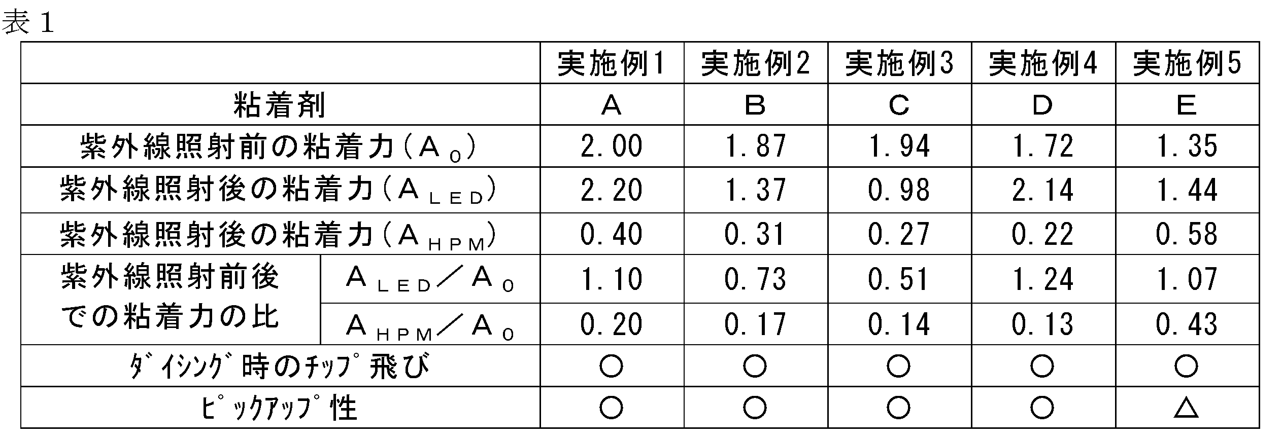
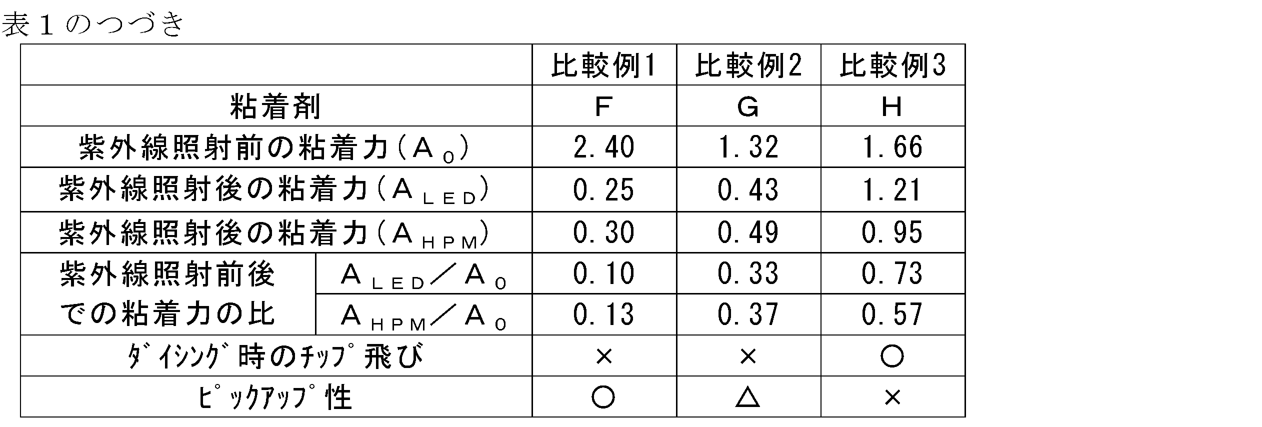
実施例1~5の粘着テープは、本発明で規定する、(1)[紫外線照射前の粘着力]に対する[波長365nmのLEDランプを光源とする紫外線照射装置による積算光量500mJ/cm2の紫外線照射後の粘着力]の比(ALED/A0)が0.50以上の値を有し、(2)[紫外線照射前の粘着力]に対する[高圧水銀ランプを光源とする紫外線照射装置による積算光量500mJ/cm2の紫外線照射後の粘着力]の比(AHPM/A0)が0.50以下の値を有する。
これらの実施例1~5の紫外線照射型粘着テープは、半導体ウェハの一方の面に貼合して使用した場合に、波長365nmのLEDランプを光源とする紫外線照射後にダイシングを行っても、ダイシング時のチップ飛びを抑制することができることがわかった。さらに、上記ダイシング後に、高圧水銀ランプを光源とする紫外線を照射し、その後ピックアップを行うことにより、紫外線照射型粘着テープからチップを良好に剥離できることがわかった。つまり、これらの実施例1~5の紫外線照射型粘着テープは、チップ飛びの抑制とピックアップ性の両立に優れることがわかった。
実施例1~5についてみると、[紫外線照射前の粘着力]に対する[高圧水銀ランプを光源とする紫外線照射装置による積算光量500mJ/cm2の紫外線照射後の粘着力]の比(AHPM/A0)が0.43である実施例5の粘着テープを用いた場合には、ピックアップ工程時に粘着テープ上に12チップが残ったのに対し、上記比(AHPM/A0)が0.40以下である実施例1~4の粘着テープを用いた場合には、ピックアップ工程時に粘着テープ上にチップが1つも残らず、ピックアップ性により優れることがわかった。
比較例2の粘着テープは、本発明で規定する(2)を満たすものの、[紫外線照射前の粘着力]に対する[波長365nmのLEDランプを光源とする紫外線照射装置による積算光量500mJ/cm2の紫外線照射後の粘着力]の比(ALED/A0)が0.33であり、本発明で規定する0.50以上を満たさない。この比較例2の粘着テープは、波長365nmのLEDランプを光源とする紫外線照射後のダイシングによるチップの飛散が見られ、チップ飛びの抑制が十分でなかった。なお、ピックアップ工程時には、粘着テープ上に4チップが残った。
比較例3の粘着テープは、本発明で規定する(1)を満たすものの、(2)[紫外線照射前の粘着力]に対する[高圧水銀ランプを光源とする紫外線照射装置による積算光量500mJ/cm2の紫外線照射後の粘着力]の比(AHPM/A0)が0.57であり、本発明で規定する0.50以下を満たさない。この比較例3の粘着テープは、LEDランプを光源とする紫外線照射後にダイシングを行い、次いで、高圧水銀ランプを光源とする紫外線を照射し、ピックアップを行った際には、1238枚の全てのチップが粘着テープ上に残り、ピックアップ性が十分でなかった。
また、本発明の粘着テープを使用することにより、チップ飛びの抑制と優れたピックアップ性を両立しながら、半導体チップを製造することができる。
1A 裏面研削中の半導体ウェハ
1B 裏面が研削された状態の半導体ウェハ
1C 分割された半導体ウェハ
2 半導体ウェハ加工用紫外線硬化型粘着テープ(粘着テープ)
3 基材フィルム
4 粘着剤層
7 チップ
11 表面保護テープ
12 基材フィルム
13 粘着剤層
S 表面
B 裏面
M1 ウェハ研削装置
D ダイシングブレード
F リングフレーム
UVS1 波長365nmのLEDランプを光源とする紫外線照射装置
UVS2 高圧水銀ランプを光源とする紫外線照射装置
Claims (15)
- 基材フィルムと、該基材フィルム上に設けられた紫外線硬化型の粘着剤層とを少なくとも有する半導体ウェハ加工用紫外線硬化型粘着テープであって、
JIS Z 0237に基づくSUS304に対する90°引きはがし試験方法により測定される前記粘着テープの粘着力の値が、下記(1)及び(2)を共に満たすことを特徴とする、半導体ウェハ加工用紫外線硬化型粘着テープ。
(1)[波長365nmのLEDランプを光源とする紫外線照射装置による積算光量500mJ/cm2の紫外線照射後の粘着力]/[紫外線照射前の粘着力]≧0.50
(2)[高圧水銀ランプを光源とする紫外線照射装置による積算光量500mJ/cm2の紫外線照射後の粘着力]/[紫外線照射前の粘着力]≦0.50 - 前記[紫外線照射前の粘着力]が、1N/25mm~10N/25mmであることを特徴とする、請求項1に記載の半導体ウェハ加工用紫外線硬化型粘着テープ。
- 前記粘着剤層がベースポリマー成分と光重合開始剤とを含有し、該ベースポリマー成分100質量部に対する光重合開始剤の含有量が0.1~3.0質量部であることを特徴とする、請求項1又は2に記載の半導体ウェハ加工用紫外線硬化型粘着テープ。
- 前記ベースポリマーが側鎖に紫外線重合性炭素-炭素二重結合を有するポリマーであることを特徴とする、請求項1~3のいずれか1項に記載の半導体ウェハ加工用紫外線硬化型粘着テープ。
- 前記粘着剤層が紫外線吸収剤を含有することを特徴とする、請求項1~4のいずれか1項に記載の半導体ウェハ加工用紫外線硬化型粘着テープ。
- 半導体ウェハをダイシングする工程において使用されることを特徴とする、請求項1~5のいずれか1項に記載の半導体ウェハ加工用紫外線硬化型粘着テープ。
- 下記工程(a)~(e)を含むことを特徴とする、半導体チップの製造方法。
〔工程〕
(a)表面にパターン面を有する半導体ウェハの該パターン面側に、紫外線硬化型表面保護テープを貼り合せた状態で、該半導体ウェハの裏面を研削する工程、
(b)前記の研削した半導体ウェハの裏面に請求項1~6のいずれか1項に記載の半導体ウェハ加工用紫外線硬化型粘着テープを貼り合わせ、リングフレームに支持固定する工程、
(c)前記表面保護テープ側から、第1の紫外線照射装置により紫外線照射を行った後、前記表面保護テープを剥離する工程、
(d)前記半導体ウェハのパターン面側からダイシング装置を用いて、半導体ウェハの切断を行い、個々のチップ単位に個片化する工程、および、
(e)前記粘着テープ側から、第2の紫外線照射装置により紫外線照射を行う工程。 - 前記第1の紫外線照射装置が、波長365nmのLEDランプを光源とする紫外線照射装置であることを特徴とする、請求項7に記載の半導体チップの製造方法。
- 前記第2の紫外線照射装置が、高圧水銀ランプを光源とする紫外線照射装置であることを特徴とする、請求項7または8に記載の半導体チップの製造方法。
- 半導体ウェハの一方の面に紫外線硬化型表面保護テープが貼合され、該半導体ウェハのもう一方の面に請求項1~6のいずれか1項に記載の半導体ウェハ加工用紫外線硬化型粘着テープが貼合された半導体ウェハに対して、該紫外線硬化型表面保護テープ側から紫外線を照射する工程を含むことを特徴とする、半導体ウェハ加工用紫外線硬化型粘着テープの使用方法。
- 前記紫外線照射が波長365nmのLEDランプを光源とする紫外線照射であることを特徴とする、請求項10に記載の半導体ウェハ加工用紫外線硬化型粘着テープの使用方法。
- 前記の紫外線照射後の紫外線硬化型表面保護テープを前記半導体ウェハから剥離する工程を含むことを特徴とする、請求項10または11に記載の半導体ウェハ加工用紫外線硬化型粘着テープの使用方法。
- 前記の半導体ウェハから紫外線硬化型表面保護テープを剥離する工程の後、該半導体ウェハ加工用紫外線硬化型粘着テープ側から紫外線を照射する工程を含むことを特徴とする、請求項12に記載の半導体ウェハ加工用紫外線硬化型粘着テープの使用方法。
- 前記の半導体ウェハ加工用紫外線硬化型粘着テープ側からの紫外線照射が高圧水銀ランプを光源とする紫外線照射であることを特徴とする、請求項13に記載の半導体ウェハ加工用紫外線硬化型粘着テープの使用方法。
- 前記の、半導体ウェハの一方の面に紫外線硬化型表面保護テープが貼合され、該半導体ウェハのもう一方の面に請求項1~6のいずれか1項に記載の半導体ウェハ加工用紫外線硬化型粘着テープが貼合された半導体ウェハが、半導体ウェハの加工工程において生じるものである、請求項10~14のいずれか1項に記載の半導体ウェハ加工用紫外線硬化型粘着テープの使用方法。
Priority Applications (6)
| Application Number | Priority Date | Filing Date | Title |
|---|---|---|---|
| PH1/2020/500650A PH12020500650B1 (en) | 2019-01-25 | 2020-01-24 | Ultraviolet light-curable pressure-sensitive adhesive tape for semiconductor wafer processing, method for manufacturing semiconductor chip and method for using ultraviolet light-curable pressure-sensitive adhesive tape |
| JP2020526660A JP7444773B2 (ja) | 2019-01-25 | 2020-01-24 | 半導体ウェハ加工用紫外線硬化型粘着テープ及び半導体チップの製造方法並びにこのテープの使用方法 |
| MYPI2020004571A MY202880A (en) | 2019-01-25 | 2020-01-24 | Ultraviolet curable temporary-adhesive tape for processing semiconductor wafer, method of producing semiconductor chip, and method of using this tape |
| CN202080001315.1A CN111742026B (zh) | 2019-01-25 | 2020-01-24 | 半导体晶片加工用紫外线固化型胶带和半导体芯片的制造方法以及该带的使用方法 |
| SG11202008196WA SG11202008196WA (en) | 2019-01-25 | 2020-01-24 | Ultraviolet curable temporary-adhesive tape for processing semiconductor wafer, method of producing semiconductor chip, and method of using this tape |
| KR1020207021951A KR102452862B1 (ko) | 2019-01-25 | 2020-01-24 | 반도체 웨이퍼 가공용 자외선 경화형 점착 테이프 및 반도체 칩의 제조 방법과 이 테이프의 사용 방법 |
Applications Claiming Priority (2)
| Application Number | Priority Date | Filing Date | Title |
|---|---|---|---|
| JP2019011418 | 2019-01-25 | ||
| JP2019-011418 | 2019-01-25 |
Publications (1)
| Publication Number | Publication Date |
|---|---|
| WO2020153499A1 true WO2020153499A1 (ja) | 2020-07-30 |
Family
ID=71735725
Family Applications (1)
| Application Number | Title | Priority Date | Filing Date |
|---|---|---|---|
| PCT/JP2020/002617 Ceased WO2020153499A1 (ja) | 2019-01-25 | 2020-01-24 | 半導体ウェハ加工用紫外線硬化型粘着テープ及び半導体チップの製造方法並びにこのテープの使用方法 |
Country Status (8)
| Country | Link |
|---|---|
| JP (1) | JP7444773B2 (ja) |
| KR (1) | KR102452862B1 (ja) |
| CN (1) | CN111742026B (ja) |
| MY (1) | MY202880A (ja) |
| PH (1) | PH12020500650B1 (ja) |
| SG (1) | SG11202008196WA (ja) |
| TW (1) | TWI846807B (ja) |
| WO (1) | WO2020153499A1 (ja) |
Cited By (2)
| Publication number | Priority date | Publication date | Assignee | Title |
|---|---|---|---|---|
| JP2021155690A (ja) * | 2019-12-27 | 2021-10-07 | 日東電工株式会社 | 粘着シート |
| JP2023017527A (ja) * | 2021-07-26 | 2023-02-07 | 日東電工株式会社 | 光硬化性粘着シート |
Families Citing this family (4)
| Publication number | Priority date | Publication date | Assignee | Title |
|---|---|---|---|---|
| TWI904292B (zh) * | 2020-12-04 | 2025-11-11 | 日商力森諾科股份有限公司 | 固化性樹脂膜、半導體裝置製造用膜材料、半導體裝置製造用固化性樹脂組成物、及製造半導體裝置之方法 |
| CN116457206A (zh) * | 2021-03-26 | 2023-07-18 | 琳得科株式会社 | 工件处理片及器件制造方法 |
| KR102992401B1 (ko) * | 2022-01-26 | 2026-07-21 | 주식회사 엘지화학 | 반도체 공정용 점착 조성물, 이를 포함하는 반도체 공정용 필름 및 이를 이용한 반도체 패키지 제조 방법 |
| CN116804134A (zh) * | 2022-03-18 | 2023-09-26 | 北京小米移动软件有限公司 | 粘接胶、双面胶带及其制备方法、器件的拆卸方法 |
Citations (6)
| Publication number | Priority date | Publication date | Assignee | Title |
|---|---|---|---|---|
| JP2005086074A (ja) * | 2003-09-10 | 2005-03-31 | Disco Abrasive Syst Ltd | 半導体ウェーハの移し替え方法 |
| JP2010129607A (ja) * | 2008-11-25 | 2010-06-10 | Nitto Denko Corp | ダイシング用表面保護テープ及びダイシング用表面保護テープの剥離除去方法 |
| JP2011210944A (ja) * | 2010-03-30 | 2011-10-20 | Furukawa Electric Co Ltd:The | 帯電防止性半導体加工用粘着テープ |
| WO2014142085A1 (ja) * | 2013-03-11 | 2014-09-18 | リンテック株式会社 | 粘着シートおよび加工されたデバイス関連部材の製造方法 |
| JP2017155074A (ja) * | 2016-02-29 | 2017-09-07 | リンテック株式会社 | 粘着シートおよび光学製品の製造方法 |
| JP2019163412A (ja) * | 2018-03-20 | 2019-09-26 | リンテック株式会社 | 粘着剤の硬化方法、及び粘着剤の硬化装置 |
Family Cites Families (6)
| Publication number | Priority date | Publication date | Assignee | Title |
|---|---|---|---|---|
| JP4309671B2 (ja) | 2003-01-30 | 2009-08-05 | 三井化学株式会社 | 半導体ウェハ裏面研削用粘着フィルム及びそれを用いる半導体ウェハ裏面研削方法 |
| JP5480415B1 (ja) * | 2012-10-11 | 2014-04-23 | 古河電気工業株式会社 | 半導体ウェハ加工用粘着テープ |
| JP2014111715A (ja) | 2012-10-31 | 2014-06-19 | Nitto Denko Corp | 紫外線硬化型アクリル系粘着剤層を有する粘着シートの製造方法 |
| JPWO2014080918A1 (ja) * | 2012-11-20 | 2017-01-05 | 古河電気工業株式会社 | 半導体チップの製造方法およびそれに用いる薄膜研削用表面保護テープ |
| JP6490459B2 (ja) * | 2015-03-13 | 2019-03-27 | 古河電気工業株式会社 | ウェハ固定テープ、半導体ウェハの処理方法および半導体チップ |
| JP6917166B2 (ja) * | 2017-03-15 | 2021-08-11 | マクセルホールディングス株式会社 | ダイシング用粘着テープ、ダイシング用粘着テープの製造方法、および半導体チップの製造方法 |
-
2020
- 2020-01-22 TW TW109102397A patent/TWI846807B/zh active
- 2020-01-24 MY MYPI2020004571A patent/MY202880A/en unknown
- 2020-01-24 KR KR1020207021951A patent/KR102452862B1/ko active Active
- 2020-01-24 SG SG11202008196WA patent/SG11202008196WA/en unknown
- 2020-01-24 JP JP2020526660A patent/JP7444773B2/ja active Active
- 2020-01-24 WO PCT/JP2020/002617 patent/WO2020153499A1/ja not_active Ceased
- 2020-01-24 PH PH1/2020/500650A patent/PH12020500650B1/en unknown
- 2020-01-24 CN CN202080001315.1A patent/CN111742026B/zh active Active
Patent Citations (6)
| Publication number | Priority date | Publication date | Assignee | Title |
|---|---|---|---|---|
| JP2005086074A (ja) * | 2003-09-10 | 2005-03-31 | Disco Abrasive Syst Ltd | 半導体ウェーハの移し替え方法 |
| JP2010129607A (ja) * | 2008-11-25 | 2010-06-10 | Nitto Denko Corp | ダイシング用表面保護テープ及びダイシング用表面保護テープの剥離除去方法 |
| JP2011210944A (ja) * | 2010-03-30 | 2011-10-20 | Furukawa Electric Co Ltd:The | 帯電防止性半導体加工用粘着テープ |
| WO2014142085A1 (ja) * | 2013-03-11 | 2014-09-18 | リンテック株式会社 | 粘着シートおよび加工されたデバイス関連部材の製造方法 |
| JP2017155074A (ja) * | 2016-02-29 | 2017-09-07 | リンテック株式会社 | 粘着シートおよび光学製品の製造方法 |
| JP2019163412A (ja) * | 2018-03-20 | 2019-09-26 | リンテック株式会社 | 粘着剤の硬化方法、及び粘着剤の硬化装置 |
Cited By (4)
| Publication number | Priority date | Publication date | Assignee | Title |
|---|---|---|---|---|
| JP2021155690A (ja) * | 2019-12-27 | 2021-10-07 | 日東電工株式会社 | 粘着シート |
| JP7566490B2 (ja) | 2019-12-27 | 2024-10-15 | 日東電工株式会社 | 粘着シート |
| JP2023017527A (ja) * | 2021-07-26 | 2023-02-07 | 日東電工株式会社 | 光硬化性粘着シート |
| JP7696246B2 (ja) | 2021-07-26 | 2025-06-20 | 日東電工株式会社 | 光硬化性粘着シート |
Also Published As
| Publication number | Publication date |
|---|---|
| KR102452862B1 (ko) | 2022-10-12 |
| JP7444773B2 (ja) | 2024-03-06 |
| KR20200104384A (ko) | 2020-09-03 |
| CN111742026B (zh) | 2022-05-24 |
| MY202880A (en) | 2024-05-28 |
| PH12020500650B1 (en) | 2023-09-27 |
| TW202037694A (zh) | 2020-10-16 |
| TWI846807B (zh) | 2024-07-01 |
| SG11202008196WA (en) | 2020-09-29 |
| CN111742026A (zh) | 2020-10-02 |
| PH12020500650A1 (en) | 2021-06-07 |
| JPWO2020153499A1 (ja) | 2021-12-02 |
Similar Documents
| Publication | Publication Date | Title |
|---|---|---|
| JP7444773B2 (ja) | 半導体ウェハ加工用紫外線硬化型粘着テープ及び半導体チップの製造方法並びにこのテープの使用方法 | |
| JP5823591B1 (ja) | 半導体ウエハ表面保護用粘着テープおよび半導体ウエハの加工方法 | |
| KR100743772B1 (ko) | 웨이퍼 가공용 테이프 | |
| JP5731080B2 (ja) | 粘着テープおよびウエハ加工用テープ | |
| JP5294358B2 (ja) | ウエハ加工用テープ及びこれを使用した半導体装置の製造方法 | |
| JP6034522B1 (ja) | 半導体ウェハ加工用粘着テープおよび半導体ウェハの加工方法 | |
| JP5117630B1 (ja) | 半導体ウェハ表面保護用粘着テープおよびそれを用いた半導体ウェハの製造方法 | |
| WO2017072901A1 (ja) | 半導体ウエハ表面保護用粘着テープおよび半導体ウエハの加工方法 | |
| JP5158864B2 (ja) | ウエハ加工用テープ | |
| JPWO2020032176A1 (ja) | 端子保護用テープ及び電磁波シールド膜付き半導体装置の製造方法 | |
| JP6917166B2 (ja) | ダイシング用粘着テープ、ダイシング用粘着テープの製造方法、および半導体チップの製造方法 | |
| JP5089358B2 (ja) | ウエハ加工用テープ | |
| JP5323779B2 (ja) | ウエハ加工用テープ | |
| WO2019181403A1 (ja) | 粘着テープおよび半導体装置の製造方法 | |
| JP2007073930A (ja) | ウエハ加工用テープ | |
| JP3495388B2 (ja) | 半導体ウエハダイシング用粘着テープ | |
| JP4712468B2 (ja) | ダイシングダイボンドテープ | |
| JP6046073B2 (ja) | 半導体ウエハ表面保護用粘着テープ | |
| CN103360972B (zh) | 半导体晶片表面保护用粘合带 | |
| WO2017046869A1 (ja) | 半導体ウエハ表面保護用粘着テープ | |
| JP2009158503A (ja) | ウエハ加工用テープ | |
| JPWO2020032175A1 (ja) | 端子保護用テープ及び電磁波シールド膜付き半導体装置の製造方法 | |
| JP5653990B2 (ja) | 半導体ウェハ表面保護用粘着テープの製造方法 | |
| JP7366435B2 (ja) | ウェハ研削用粘着テープおよびウェハの加工方法 | |
| JP5950519B2 (ja) | ウエハ加工用テープ |
Legal Events
| Date | Code | Title | Description |
|---|---|---|---|
| ENP | Entry into the national phase |
Ref document number: 2020526660 Country of ref document: JP Kind code of ref document: A |
|
| ENP | Entry into the national phase |
Ref document number: 20207021951 Country of ref document: KR Kind code of ref document: A |
|
| 121 | Ep: the epo has been informed by wipo that ep was designated in this application |
Ref document number: 20744638 Country of ref document: EP Kind code of ref document: A1 |
|
| NENP | Non-entry into the national phase |
Ref country code: DE |
|
| 122 | Ep: pct application non-entry in european phase |
Ref document number: 20744638 Country of ref document: EP Kind code of ref document: A1 |