WO2020153250A1 - モード合分波光回路 - Google Patents
モード合分波光回路 Download PDFInfo
- Publication number
- WO2020153250A1 WO2020153250A1 PCT/JP2020/001468 JP2020001468W WO2020153250A1 WO 2020153250 A1 WO2020153250 A1 WO 2020153250A1 JP 2020001468 W JP2020001468 W JP 2020001468W WO 2020153250 A1 WO2020153250 A1 WO 2020153250A1
- Authority
- WO
- WIPO (PCT)
- Prior art keywords
- mode
- waveguide
- input
- order
- light
- Prior art date
- Legal status (The legal status is an assumption and is not a legal conclusion. Google has not performed a legal analysis and makes no representation as to the accuracy of the status listed.)
- Ceased
Links
Images



Classifications
-
- G—PHYSICS
- G02—OPTICS
- G02B—OPTICAL ELEMENTS, SYSTEMS OR APPARATUS
- G02B6/00—Light guides; Structural details of arrangements comprising light guides and other optical elements, e.g. couplings
- G02B6/10—Light guides; Structural details of arrangements comprising light guides and other optical elements, e.g. couplings of the optical waveguide type
- G02B6/12—Light guides; Structural details of arrangements comprising light guides and other optical elements, e.g. couplings of the optical waveguide type of the integrated circuit kind
- G02B6/12007—Light guides; Structural details of arrangements comprising light guides and other optical elements, e.g. couplings of the optical waveguide type of the integrated circuit kind forming wavelength selective elements, e.g. multiplexer, demultiplexer
-
- G—PHYSICS
- G02—OPTICS
- G02B—OPTICAL ELEMENTS, SYSTEMS OR APPARATUS
- G02B6/00—Light guides; Structural details of arrangements comprising light guides and other optical elements, e.g. couplings
- G02B6/10—Light guides; Structural details of arrangements comprising light guides and other optical elements, e.g. couplings of the optical waveguide type
- G02B6/12—Light guides; Structural details of arrangements comprising light guides and other optical elements, e.g. couplings of the optical waveguide type of the integrated circuit kind
- G02B6/122—Basic optical elements, e.g. light-guiding paths
- G02B6/125—Bends, branchings or intersections
-
- G—PHYSICS
- G02—OPTICS
- G02B—OPTICAL ELEMENTS, SYSTEMS OR APPARATUS
- G02B6/00—Light guides; Structural details of arrangements comprising light guides and other optical elements, e.g. couplings
- G02B6/10—Light guides; Structural details of arrangements comprising light guides and other optical elements, e.g. couplings of the optical waveguide type
- G02B6/14—Mode converters
-
- G—PHYSICS
- G02—OPTICS
- G02B—OPTICAL ELEMENTS, SYSTEMS OR APPARATUS
- G02B6/00—Light guides; Structural details of arrangements comprising light guides and other optical elements, e.g. couplings
- G02B6/10—Light guides; Structural details of arrangements comprising light guides and other optical elements, e.g. couplings of the optical waveguide type
- G02B6/12—Light guides; Structural details of arrangements comprising light guides and other optical elements, e.g. couplings of the optical waveguide type of the integrated circuit kind
- G02B2006/12133—Functions
- G02B2006/12147—Coupler
-
- G—PHYSICS
- G02—OPTICS
- G02B—OPTICAL ELEMENTS, SYSTEMS OR APPARATUS
- G02B6/00—Light guides; Structural details of arrangements comprising light guides and other optical elements, e.g. couplings
- G02B6/10—Light guides; Structural details of arrangements comprising light guides and other optical elements, e.g. couplings of the optical waveguide type
- G02B6/12—Light guides; Structural details of arrangements comprising light guides and other optical elements, e.g. couplings of the optical waveguide type of the integrated circuit kind
- G02B2006/12133—Functions
- G02B2006/12152—Mode converter
-
- G—PHYSICS
- G02—OPTICS
- G02B—OPTICAL ELEMENTS, SYSTEMS OR APPARATUS
- G02B6/00—Light guides; Structural details of arrangements comprising light guides and other optical elements, e.g. couplings
- G02B6/10—Light guides; Structural details of arrangements comprising light guides and other optical elements, e.g. couplings of the optical waveguide type
- G02B6/12—Light guides; Structural details of arrangements comprising light guides and other optical elements, e.g. couplings of the optical waveguide type of the integrated circuit kind
- G02B2006/12133—Functions
- G02B2006/12164—Multiplexing; Demultiplexing
-
- G—PHYSICS
- G02—OPTICS
- G02B—OPTICAL ELEMENTS, SYSTEMS OR APPARATUS
- G02B6/00—Light guides; Structural details of arrangements comprising light guides and other optical elements, e.g. couplings
- G02B6/10—Light guides; Structural details of arrangements comprising light guides and other optical elements, e.g. couplings of the optical waveguide type
- G02B6/12—Light guides; Structural details of arrangements comprising light guides and other optical elements, e.g. couplings of the optical waveguide type of the integrated circuit kind
- G02B6/122—Basic optical elements, e.g. light-guiding paths
- G02B6/1228—Tapered waveguides, e.g. integrated spot-size transformers
Definitions
- the present invention relates to an optical device, and more specifically to a mode multiplexing/demultiplexing optical circuit.
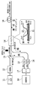
- the continuous light in the 1.0 ⁇ m band from the light source 11 is input to the converter 12 including an acousto-optic device and is pulsed.
- the pulse signal from the converter 12 is input to the Port 2 of the mode converter (mode coupler) 14 via the optical circulator 13.
- the pulse signal input to Port2 of the mode coupler 14 is converted from the 0th-order mode to the 1st-order mode, and is output from Port3.
- the pulse signal converted into the primary mode propagates through the laying fiber 19 connected to Port 3 of the mode coupler 14.
- the backscattered light generated at the deteriorated portion of the laying fiber 19 is input to the Port 3 of the mode coupler 14 again.
- the backscattered light output from Prot1 and Prot2 of the mode coupler 14 is photoelectrically converted by the photodiodes 15 and 16, respectively.
- the electric output from the photodiodes 15 and 16 is converted into a digital signal by the A/D converter 17.
- An arithmetic processing unit 18 such as a computer performs OTDR (Optical Time Domain Reflectometer) on the digital signal to estimate a fiber degradation point.
- OTDR Optical Time Domain Reflectometer
- the conventional mode coupler can be realized by an asymmetric directional coupler having different waveguide widths using a silica-based planar lightwave circuit (PLC).
- PLC planar lightwave circuit
- a PLC is a planar substrate that is patterned by photolithography and etched to form an optical waveguide with a core and a clad having a refractive index lower than that of the core, and a plurality of basic optical circuits (eg, directional coupling).
- Various functions are realized by combining the instrument, Mach-Zehnder interferometer, etc.).
- ⁇ , W, ⁇ , and m represent wavelength, waveguide width, refractive index difference, and mode order, respectively.
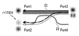
- the 0th-order mode light propagating in the thicker waveguide 21 of the mode coupler does not have the same propagation constant as the 0th-order mode light propagating in the thinner waveguide 22. Pass through as it is (solid line arrow extending between Port1 and Port3 in FIG. 2).
- the first-order mode light propagating in the thicker waveguide 21 of the mode coupler is converted into the 0th-order mode light and is coupled to the thinner waveguide 22 or propagates in the thinner waveguide 22.
- the light of the next mode is converted into the light of the first mode and is coupled to the thicker waveguide 21 (indicated by a dotted hollow arrow extending between Port1 and Port3 in FIG. 2).
- Patent Document 1 Japanese Patent Laid-Open No. 2005-152399
- FIG. 3 is a diagram showing how the light input from Port 3 is multiplexed/demultiplexed into Port 1 and Port 2 in the mode coupler.
- the 0th-order mode light propagating in the thicker waveguide 21 of the mode coupler does not have the same propagation constant as the 0th-order mode light propagating in the thinner waveguide 22. Therefore, most of it passes through as it is (in FIG. 3, a solid line arrow from Port3 to Port1).
- a few% of the 0th-order mode light propagating through the thicker waveguide 21 of the mode coupler is converted into the 1st-order mode light and is coupled to the thinner waveguide 22 (from Port 3 to Port 2 in FIG. 3). Dash-dotted arrow pointing to). Therefore, in the configuration of the mode coupler shown in FIG. 1, there is a problem that the extinction ratio between the 0th-order mode component and the 1st-order mode component is deteriorated at the time of demultiplexing.
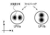
- FIG. 4 is a diagram showing the distribution of the primary mode propagating in the fiber.
- the backscattered light propagating through the laying fiber 19 includes LP11a having two peaks of light intensity in the x direction, LP11b having two peaks in the y direction, and a zero-order mode (not shown) as shown in FIG.
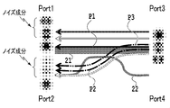
- FIG. 5 is a diagram showing a relationship between input and output when the backscattered light of three modes input from Port3 is multiplexed/demultiplexed into Port1 and Port2 in the mode coupler, and is a diagram collectively showing the above-mentioned contents. ..
- solid line arrows from Port3 to Port1 indicate most of the backscattered light that is output without being converted from the 0th-order mode (port 1 signal component).
- the solid white arrow from Port3 to Port1 indicates most of the backscattered light LP11b that is output without being converted from the first-order mode (noise component of Port1).
- a solid gray arrow heading from Port3 to Port1 indicates a part of the backscattered light LP11a that is output without being converted from the primary mode (a noise component of Port1).
- a dotted white arrow from Port3 to Port2 indicates most of the backscattered light LP11a that is output after being converted from the first-order mode light to the zero-order mode light (port 2 signal component).
- An alternate long and short dash line arrow P2 from Port3 to Port2 indicates part of the backscattered light that is output without being converted from the 0th-order mode (a noise component of Port2).
- the double-dashed line arrow from Port3 to Port2 indicates a part of the backscattered light LP11b that is converted from the first-order mode to the zero-order mode and output (a noise component of Port2).
- the noise component (hereinafter referred to as intermode crosstalk) between the desired signal component and It is necessary to have a high extinction ratio mode coupler that suppresses
- the present invention has been made in view of such problems, and an object thereof is to provide a mode multiplexing/demultiplexing optical circuit in which crosstalk between modes is suppressed.
- an aspect of the present invention is a mode multiplexing/demultiplexing optical circuit.
- a mode multiplexing/demultiplexing optical circuit includes a first waveguide and a second waveguide formed on a planar lightwave circuit, and a light from a light source is input to the first waveguide.
- the first input/output port, the second input/output port for outputting the light propagating through the first waveguide, and the mode converter disposed adjacent to the first waveguide, and the second input/output port A mode converter that converts the mode of light input from the output port to a higher order than the mode when input to the second input/output port, and a second waveguide disposed adjacent to the mode converter A third output port for converting the light input to the mode conversion unit to a lower order than the mode at the time of being input to the second input/output port.
- FIG. 9 is a diagram showing how the conventional mode coupler shown in FIG. 2 multiplexes and demultiplexes light input from Port3 into Port1 and Port2. It is a figure which shows the distribution of the 1st-order mode which propagates a fiber.
- FIG. 8 is a diagram showing an input/output relationship when the backscattered light of three modes input from Port 3 is multiplexed/demultiplexed into Port 1 and Port 2 in the conventional mode coupler of FIG. 2.
- FIG. 6 is a diagram showing inter-mode crosstalk which becomes a noise component in OTDR when the mode coupler having the input/output relationship shown in FIG. 5 is used. It is a figure for explaining a mode coupler concerning one embodiment of the invention in this application. It is a figure which shows the relationship between a waveguide width and an effective refractive index. It is a figure which shows the mode of propagation of the light in the mode coupler of FIG.
- FIG. 8 is a diagram showing the transmittances of Port 2 to Port 3 of the mode coupler of FIG. 7.
- FIG. 6 is a diagram showing crosstalk between modes which becomes a noise component in the OTDR when the mode coupler having the input/output relationship shown in FIG. 5 is used. As shown in FIG. 6, there are four types of crosstalk between modes that are noise components.
- the high-order component output to Port1 can be removed by disposing a mode filter having a thin waveguide so that the single mode condition is satisfied, and therefore crosstalk to Port2 will be considered.
- Port3 (0th order) to Port1 (0th order) is P1
- the output from Port3 (0th order) to Port2 (0th order) is P2
- the output from Port3 (LP11b) to Port2 (0th order) is P3.
- (P2+P3)/P1 is defined as the inter- mode crosstalk XT mode .
- the mode coupler 70 shown in FIG. 7 is an asymmetrical directional coupler having two waveguides 71 and 72. One end of the thicker waveguide 71 is set to Port1 and the other end is set to Port3. One end of the narrower waveguide 72 is Port2, and the other end is Port4. Between the waveguide 71 and the waveguide 72, a waveguide 73 is arranged as a mode converter so as to be adjacent to each other. In the mode coupler 70, the mode filter 74 is arranged on the Port 71 side of the waveguide 71 with respect to the position where the waveguide 73 is adjacent.
- the mode filter 74 is a tapered waveguide in which the width of the waveguide 71 is narrowed so as to meet the single mode condition. Output from Port1.
- the mode coupler 70 can be realized by using a silica-based planar lightwave circuit (PLC).
- PLC planar lightwave circuit
- W 0 indicates the waveguide width of the thinner waveguide 72
- W 1 indicates the waveguide width of the thicker waveguide 71
- W 2 indicates the waveguide width of the waveguide 73. ..
- the mode coupler 14 converts the pulse signal input to the Port 2 from the 0th order mode to a desired higher order mode and outputs it from the Port 3. There is no higher order mode other than the 0th and desired higher order modes in this conversion. That is, conventionally, the mode coupler 14 directly converts from the 0th order mode to the desired higher order mode.
- another mode is sandwiched between the 0th order and the desired higher order mode to enhance the isolation between the modes. More specifically, in the mode coupler 70 of the present embodiment, by disposing the waveguide 73 between the waveguide 71 and the waveguide 72, in the conversion between the 0th order and the desired higher order mode. , 0th order and higher order modes other than the desired higher order mode are interposed.
- the core thickness of the waveguide is 5.6 ⁇ m
- the refractive index difference ⁇ between the core and the clad is 0.42%
- the mode conversion is between the 0th order and the 2nd order and between the 2nd order and the 1st order.
- the operating wavelength is 1050 nm.
- FIG. 8 is a diagram showing the relationship between the waveguide width and the effective refractive index.
- W 0 3.5 ⁇ m
- W 1 10.1 ⁇ m
- W 2 16.4 ⁇ m are determined.
- FIG. 9 is a diagram showing how light propagates when the mode coupler 70 of FIG. 7 is configured using the above-described numerical example. As intended, it can be seen that in the mode coupler 70, the light input to Port2 is converted from 0th order to 2nd order, then from 2nd order to 1st order, and output to Port3.
- FIG. 10 is a diagram showing the transmittance of Port 2 to Port 3.
- Three-dimensional BPM Beam Propagation Method
- the mode coupler 70 is configured such that the light input to the Port 2 is converted from the 0th order to the 2nd order and then from the 2nd order to the 1st order. It goes without saying that it is not limited to the intermediate mode order.
Landscapes
- Physics & Mathematics (AREA)
- General Physics & Mathematics (AREA)
- Optics & Photonics (AREA)
- Engineering & Computer Science (AREA)
- Microelectronics & Electronic Packaging (AREA)
- Optical Integrated Circuits (AREA)
Abstract
モード間クロストークを抑えたモード合分波光回路を提供する。モード合分波光回路において、光源からの光が導波路(71)に入力されるPort1と、第1の導波路を伝搬した光が出力されるPort3と、第1の導波路に隣接して配置された、ポート3から入力された1次モードの光を2次モードに変換するモード変換部(73)と、モード変換部に隣接して配置された導波路(72)を介して、モード変換部に入力された2次モードの光を0次モードに変換して出力するPort2とを備えた。
Description
本発明は、光デバイスに関し、より詳しくはモード合分波光回路に関する。
近年、モードの自由度を活用した光通信システムが多く提案されている。例えば、ファイバ1本当りの伝送容量拡大を目指して、空間多重伝送と呼ばれるモード毎に信号をのせる手法や、高次モードの試験光を測定対象ファイバに入射し、後方散乱光の強度から敷設ファイバの状態を監視する手法なども提案されている(例えば、特許文献1参照)。
図1を用いて、高次モードを利用した、敷設ファイバの監視方法について簡単に説明する。通常、光通信には、ファイバの伝搬損失が最も小さくなる、1.55μm帯の赤外光を利用する。敷設ファイバはこの波長に於いて、シングルモード伝搬となるようにコア径が決められている。一方で、敷設ファイバの監視に1.0μm帯の光を使用すると、0次モードと1次モードのマルチモード伝搬が可能となる。1次モードは0次モードより、マイクロベンドや亀裂などのファイバ劣化に対して敏感に反応するため、高感度なセンシングが可能となる。
図1に示すように、光源11からの1.0μm帯の連続光は、音響光学素子等を含んで構成された変換器12へ入力され、パルス化される。変換器12からのパルス信号は、光サーキュレータ13を介して、モード変換器(モードカプラ)14のPort2へ入力される。モードカプラ14のPort2へ入力されたパルス信号は、0次モードから1次モードへ変換されて、Port3から出力される。1次モードへ変換されたパルス信号は、モードカプラ14のPort3に接続された敷設ファイバ19を伝搬する。
敷設ファイバ19における劣化箇所で発生した後方散乱光は、再びモードカプラ14のPort3へ入力される。モードカプラ14のProt1,Prot2から出力された後方散乱光は、フォトダイオード15,16でそれぞれ光電変換される。フォトダイオード15,16からの電気出力は、A/D変換器17でデジタル信号に変換される。コンピュータなどの演算処理装置18で、デジタル信号をOTDR(Optical Time Domain Reflectometer)することで、ファイバの劣化箇所を推定する。モードの合分波には、平面光波回路を用いたモードカプラを用いている。
図2に示す様に、従来のモードカプラは、石英系平面光波回路(Planar Lightwave Circuit:PLC)を用いた異なる導波路幅から成る非対称な方向性結合器で実現できる。PLCは、平面状の基板に、フォトリソグラフィなどによるパターニングと、エッチング加工により、コアと屈折率がコアよりも低いクラッドで光導波路を作製し、複数の基本的な光回路(例:方向性結合器、マッハ・ツェンダー干渉計など)を組み合わせることで各種の機能を実現する。モードカプラは、細い方の導波路22を伝搬する0次モード光の伝搬定数β(λ,W0,Δ)m=0と太い方の導波路21を伝搬する高次モード光の伝搬定数β(λ,W1,Δ)m=1とを一致させ、モードカプラの長さを適切に設定することで、0次モードの光と高次モードの光とを、約100%変換可能である。ここで、λ、W、Δ、mはそれぞれ、波長、導波路幅、屈折率差、モード次数を表す。
図2に示すように、モードカプラの太い方の導波路21を伝搬する0次モードの光は、細い方の導波路22を伝搬する0次モードの光と伝搬定数が一致しないため大部分はそのまま通過する(図2においてPort1とPort3との間に伸びる実線の矢印)。モードカプラの太い方の導波路21を伝搬する1次モードの光は、0次モードの光に変換されて、細い方の導波路22に結合する、または細い方の導波路22を伝搬する0次モードの光は、1次モードの光に変換されて、太い方の導波路21に結合する(図2においてPort1とPort3との間に伸びる点線白抜の矢印)。
図3はモードカプラにおいて、Port3から入力した光をPort1およびPort2へ合分波する様子を示す図である。図2を参照して説明したように、モードカプラの太い方の導波路21を伝搬する0次モードの光は、細い方の導波路22を伝搬する0次モードの光と伝搬定数が一致しないため大部分はそのまま通過する(図3においてPort3からPort1へ向かう実線の矢印)。しかしながら、モードカプラの太い方の導波路21を伝搬する0次モードの光の数%は、1次モードの光に変換されて、細い方の導波路22に結合する(図3においてPort3からPort2へ向かう一点鎖線の矢印)。そのため、図1に示したモードカプラの構成において、分波の際に0次と1次モード成分との間の消光比が劣化するといった課題がある。
同様に、図3のPort1には0次モード成分に変換されなかった高次モード成分が混ざって出力される。
図4は、ファイバを伝搬する1次モードの分布を示す図である。敷設ファイバ19を伝搬する後方散乱光には、図4の様にx方向に光強度の山が2つになるLP11aとy方向に山が2つになるLP11b、および0次モード(不図示)の3つのモードが存在する。PLCのモードカプラ14で分波できるのはLP11aのみであるのため、LP11bの大部分がそのまま透過し、LP11bの一部が0次モードに変換されてPort2に出力されてしまう。
図5は、モードカプラにおいて、Port3から入力した3つのモードの後方散乱光をPort1およびPort2へ合分波する際の入出力の関係を示す図であり、上述した内容をまとめて示す図である。
図5において、Port3からPort1へ向かう実線の矢印は、0次モードから変換されず出力される後方散乱光の大部分を示す(Port1の信号成分)。Port3からPort1へ向かう実線白抜きの矢印は、1次モードから変換されずに出力される後方散乱光LP11bの大部分を示す(Port1のノイズ成分)。Port3からPort1へ向かう実線灰色の矢印は、1次モードから変換されずに出力される後方散乱光LP11aの一部を示す(Port1のノイズ成分)。
また、図5において、Port3からPort2へ向かう点線白抜の矢印は、1次モードから0次モードの光に変換されて出力される後方散乱光LP11aの大部分を示す(Port2の信号成分)。Port3からPort2へ向かう一点鎖線の矢印P2は、0次モードから変換されず出力される後方散乱光の一部を示す(Port2のノイズ成分)。Port3からPort2へ向かう二点鎖線の矢印は、1次モードから0次モードに変換されて出力される後方散乱光LP11bの一部を示す(Port2のノイズ成分)。
上述したように、モードカプラのPort1およびPort2には信号成分とノイズ成分が出力されることから、長距離を測定するためには、所望の信号成分に対してノイズ成分(以下、モード間クロストークと呼ぶこととする)を抑えた高消光比なモードカプラが必要となる。
本発明は、このような問題に鑑みてなされたもので、その目的とするところは、モード間クロストークを抑えたモード合分波光回路を提供することにある。
このような目的を達成するために、本発明の態様は、モード合分波光回路である。一実施形態に係るモード合分波光回路は、平面光波回路上に形成された、第1の導波路および第2の導波路を備え、光源からの光が第1の導波路に入力される第1の入出力ポートと、第1の導波路を伝搬した光が出力される第2の入出力ポートと、第1の導波路に隣接して配置されたモード変換部であり、第2の入出力ポートから入力された光のモードを、第2の入出力ポートへ入力された時のモードより高い次数に変換するモード変換部と、モード変換部に隣接して配置された第2の導波路を介して、モード変換部に入力された光を第2の入出力ポートへ入力された入力された時のモードよりも低い次数に変換して出力する第3の出力ポートとを備えている。
この構成によれば、モード間クロストークを抑えたモード合分波光回路を提供することが可能となる。
以上説明したように、本発明によれば、モード間クロストークを抑えることができるため、SNの劣化を抑えられOTDRによる長距離の測定が可能となる。
以下、図面を参照しながら本発明の実施形態について詳細に説明する。以下の説明で示す数値は例示であり、本願発明は、これに限定されない。
本願発明の実施の形態を詳述する前に、モード間クロストークについて定義する。図6は、図5に示す入出力関係を有するモードカプラを用いた場合にOTDRにおいて、ノイズ成分となるモード間クロストークを示す図である。図6に示すように、ノイズ成分となるモード間クロストークは4種類存在する。Port1への高次成分の出力は、シングルモード条件となるように導波路を細くしたモードフィルタを配置することで、除去することが可能なためPort2へのクロストークを考えることとする。
Port3(0次)からPort1(0次)への出力をP1、Port3(0次)からPort2(0次)への出力をP2、Port3(LP11b)からPort2(0次)への出力をP3とすると、(P2+P3)/P1をモード間クロストークXTmodeと定義する。
図7を参照して本願発明の第1の実施の形態に係るモードカプラを説明する。図7に示すモードカプラ70は、2本の導波路71、72を有する非対称な方向性結合器である。太い方の導波路71の一端をPort1とし、他端をPort3とする。細い方の導波路72の一端をPort2とし、他端をPort4とする。導波路71と導波路72との間には、それぞれに隣接するように、モード変換部として、導波路73が配置されている。モードカプラ70は、導波路71の、導波路73が隣接する位置よりもPort1側に、モードフィルタ74が配置されている。モードフィルタ74は、導波路71の幅を、シングルモード条件となるよう細くしてテーパー導波路としたもので、Port1へ向かう高次成分を除去し、0次モードの光のみが導波してPort1から出力されるようにする。モードカプラ70は、石英系平面光波回路(Planar Lightwave Circuit:PLC)を用いて実現することができる。図7において、W0は細い方の導波路72の導波路幅を示し、W1は太い方の導波路71の導波路幅を示し、W2は導波路73の導波路幅を示している。
図1を参照して上述したように、従来、モードカプラ14は、Port2へ入力されたパルス信号を0次モードから所望の高次モードへ変換してPort3から出力していた。この変換において0次および所望の高次モード以外の高次モードは存在しない。すなわち、従来、モードカプラ14は、0次モードから所望の高次モードへ直接変換していた。
本実施の形態では、0次と所望の高次モードとの間に、別のモードを挟むことで、モード間のアイソレーションを高めている。より具体的には、本実施の形態のモードカプラ70では、導波路71と導波路72との間に導波路73を配置することで、0次と所望の高次モードとの間の変換において、0次および所望の高次モード以外の高次モードを介在するようにしている。
例として、導波路のコア厚を5.6μmとし、コアとクラッドとの間の屈折率差Δを0.42%とし、モード変換は0次と2次との間および2次と1次との間で生じるとし、動作波長を1050nmとした場合を考える。
図8は、導波路幅と実効屈折率との関係を示す図である。モード間を完全に変換するには、各モードの実効屈折率を合わせる必要がある。例えば、W0=3.5μmとした場合、W1=10.1μm、W2=16.4μmと決定される。まず、順方向(Port2からPort3へ)の伝搬を考える。
図9は、前述した数値例を用いて図7のモードカプラ70を構成した場合の、光の伝搬の様子を示す図である。狙い通り、モードカプラ70において、Port2へ入力された光は、0次から2次へ変換され、次いで2次から1次と変換され、Port3へ出力されることが分かる。
図10は、Port2からPort3の透過率を示す図である。計算は、三次元BPM(Beam Propagation Method)を用いた。動作波長1050nmにおいて、約100%の透過率が得られていることが分かる。
次に、逆方向(Port3からPort2へ)の伝搬を考える。Port3から、後方散乱光として、0dBの0次モードのLP11bを入力した場合の出力P2(Port3(0次)からPort2(0次)への出力)およびP3(Port3(LP11b)からPort2(0次)への出力)はそれぞれ、-49.0dBおよび-51.1dBであった(シミュレーション値)。直接変換型の従来のモードカプラの場合、P2およびP3は、それぞれ、-31.8dBおよび-36.3dBであるため、本実施の形態のモードカプラにおいては、モード間クロストークXTmodeが約20dBの低減されることが分かる。
上述したように、本実施の形態によれば、低モード間クロストークのモードカプラを得ることができる。本実施の形態では、Port2へ入力された光は、0次から2次へ変換され、次いで2次から1次と変換されるようモードカプラ70を構成したが、本願発明は、変換の回数や中間のモード次数に制限されないことは言うまでもない。
11 光源
12 変換器
13 光サーキュレータ
14 モードカプラ
15,16 フォトダイオード
17 A/D変換器
18 演算処理装置
19 敷設ファイバ
21,22 導波路
70 モードカプラ
71,72,73 導波路
74 モードフィルタ
12 変換器
13 光サーキュレータ
14 モードカプラ
15,16 フォトダイオード
17 A/D変換器
18 演算処理装置
19 敷設ファイバ
21,22 導波路
70 モードカプラ
71,72,73 導波路
74 モードフィルタ
Claims (4)
- 平面光波回路上に形成された、第1の導波路および第2の導波路を備えたモード合分波光回路であって、
光源からの光が前記第1の導波路に入力される第1の入出力ポートと、
前記第1の導波路を伝搬した光が出力される第2の入出力ポートと、
前記第1の導波路に隣接して配置されたモード変換部であり、前記第2の入出力ポートから入力された光のモードを、前記第2の入出力ポートへ入力された時のモードより高い次数に変換するモード変換部と、
前記モード変換部に隣接して配置された前記第2の導波路を介して、前記モード変換部に入力された光を前記第2の入出力ポートへ入力された入力された時のモードよりも低い次数に変換して出力する第3の出力ポートと
を備えた、モード合分波光回路。 - 前記光源から前記第1の入出力ポートへ入力される光は0次モードであり、
前記第2の入出力ポートから入力される光は、前記第2の入出力ポートへ入力された時に1次モードであり、前記モード変換部で2次モードに変換され、前記第2の導波路で0次モードに変換されて、前記第3の出力ポートから出力される
、請求項1に記載のモード合分波光回路。 - 前記第1の導波路の前記モード変換部が隣接する位置よりも前記第1の入出力ポート側に配置されたモードフィルタをさらに備え、前記モードフィルタは、前記第1の入出力ポートに向かって前記第1の導波路の幅を細くした構造を有する、請求項1に記載のモード合分波光回路。
- 前記第1の導波路、前記モード変換部、及び前記第2の導波路がこの順で隣接し、隣接する箇所において導波路の幅が、前記モード変換部の幅>前記第1の導波路の幅>前記第2の導波路の幅の関係を満たす、請求項1に記載のモード合分波光回路。
Priority Applications (1)
| Application Number | Priority Date | Filing Date | Title |
|---|---|---|---|
| US17/424,417 US11852863B2 (en) | 2019-01-23 | 2020-01-17 | Mode multiplexing/demultiplexing optical circuit |
Applications Claiming Priority (2)
| Application Number | Priority Date | Filing Date | Title |
|---|---|---|---|
| JP2019-009209 | 2019-01-23 | ||
| JP2019009209A JP7172642B2 (ja) | 2019-01-23 | 2019-01-23 | モード合分波光回路 |
Publications (1)
| Publication Number | Publication Date |
|---|---|
| WO2020153250A1 true WO2020153250A1 (ja) | 2020-07-30 |
Family
ID=71736078
Family Applications (1)
| Application Number | Title | Priority Date | Filing Date |
|---|---|---|---|
| PCT/JP2020/001468 Ceased WO2020153250A1 (ja) | 2019-01-23 | 2020-01-17 | モード合分波光回路 |
Country Status (3)
| Country | Link |
|---|---|
| US (1) | US11852863B2 (ja) |
| JP (1) | JP7172642B2 (ja) |
| WO (1) | WO2020153250A1 (ja) |
Families Citing this family (1)
| Publication number | Priority date | Publication date | Assignee | Title |
|---|---|---|---|---|
| JP2025009362A (ja) * | 2023-07-07 | 2025-01-20 | 富士通オプティカルコンポーネンツ株式会社 | 光検出器、光受信器及び光トランシーバ |
Citations (5)
| Publication number | Priority date | Publication date | Assignee | Title |
|---|---|---|---|---|
| US5712937A (en) * | 1994-12-01 | 1998-01-27 | Asawa; Charles K. | Optical waveguide including singlemode waveguide channels coupled to a multimode fiber |
| JP2016151660A (ja) * | 2015-02-17 | 2016-08-22 | 日本電信電話株式会社 | モード合分波器及びモード分波器の製造方法 |
| JP2017003721A (ja) * | 2015-06-09 | 2017-01-05 | 日本電信電話株式会社 | モード合分波器 |
| JP2017504830A (ja) * | 2013-12-25 | 2017-02-09 | 華為技術有限公司Huawei Technologies Co.,Ltd. | 導波路偏光スプリッタ兼偏光回転子 |
| WO2017142076A1 (ja) * | 2016-02-18 | 2017-08-24 | 日本電信電話株式会社 | 光合波回路 |
Family Cites Families (6)
| Publication number | Priority date | Publication date | Assignee | Title |
|---|---|---|---|---|
| IN190212B (ja) | 1996-07-23 | 2003-07-05 | Samsung Electronics Co Ltd | |
| EP1108235A4 (en) * | 1998-06-04 | 2005-11-09 | California Inst Of Techn | OPTICAL DEVICES BASED ON ENERGY TRANSFER BETWEEN DIFFERENT MODES IN AN OPTICAL WAVEGUIDE |
| JP6028339B2 (ja) * | 2012-02-27 | 2016-11-16 | 沖電気工業株式会社 | 波長選択性経路切換素子 |
| JP6060099B2 (ja) | 2014-02-13 | 2017-01-11 | 日本電信電話株式会社 | 光ファイバ特性解析装置および光ファイバ特性解析方法 |
| DK3167318T3 (da) | 2014-07-08 | 2022-06-13 | Univ Gent | Polarisationsuafhængig behandling ved integreret fotonik |
| EP3180643A1 (en) * | 2014-08-15 | 2017-06-21 | Corning Optical Communications LLC | Methods for coupling of waveguides with dissimilar mode field diameters, and related apparatuses, components, and systems |
-
2019
- 2019-01-23 JP JP2019009209A patent/JP7172642B2/ja active Active
-
2020
- 2020-01-17 WO PCT/JP2020/001468 patent/WO2020153250A1/ja not_active Ceased
- 2020-01-17 US US17/424,417 patent/US11852863B2/en active Active
Patent Citations (5)
| Publication number | Priority date | Publication date | Assignee | Title |
|---|---|---|---|---|
| US5712937A (en) * | 1994-12-01 | 1998-01-27 | Asawa; Charles K. | Optical waveguide including singlemode waveguide channels coupled to a multimode fiber |
| JP2017504830A (ja) * | 2013-12-25 | 2017-02-09 | 華為技術有限公司Huawei Technologies Co.,Ltd. | 導波路偏光スプリッタ兼偏光回転子 |
| JP2016151660A (ja) * | 2015-02-17 | 2016-08-22 | 日本電信電話株式会社 | モード合分波器及びモード分波器の製造方法 |
| JP2017003721A (ja) * | 2015-06-09 | 2017-01-05 | 日本電信電話株式会社 | モード合分波器 |
| WO2017142076A1 (ja) * | 2016-02-18 | 2017-08-24 | 日本電信電話株式会社 | 光合波回路 |
Also Published As
| Publication number | Publication date |
|---|---|
| JP7172642B2 (ja) | 2022-11-16 |
| JP2020118831A (ja) | 2020-08-06 |
| US20220099888A1 (en) | 2022-03-31 |
| US11852863B2 (en) | 2023-12-26 |
Similar Documents
| Publication | Publication Date | Title |
|---|---|---|
| CN114641720B (zh) | 偏振系统和方法 | |
| CA2728330C (en) | Multifaceted segmented waveguide structure for planar waveguide devices | |
| JP2007114253A (ja) | 導波路型光分岐素子 | |
| WO2017142076A1 (ja) | 光合波回路 | |
| JP2010223991A (ja) | 光波長フィルタ及び光合分波素子 | |
| CA2175886C (en) | Optical wavelength division multiplexer device | |
| JP2002286952A (ja) | 導波路型光カプラおよび該導波路型光カプラを用いた光合分波器 | |
| KR100311281B1 (ko) | 기울어진 브래그 격자와 모드 분할 방향성 결합기를 이용한 광 파장 가감기 | |
| JP7172642B2 (ja) | モード合分波光回路 | |
| CN114660718A (zh) | 一种用于小型化干涉式光纤陀螺的光子集成芯片 | |
| US20090016724A1 (en) | Multimode optical transmission system and multimode optical transmission method | |
| US8406579B2 (en) | Wavelength division multiplexing and optical modulation apparatus | |
| JP2000171663A (ja) | クラッドモ―ド結合器とブラッグファイバ格子で形成されるアッド/ドロップフィルタ―及びマルチプレクサ | |
| JP5136497B2 (ja) | 光波長フィルタ | |
| JP6697365B2 (ja) | モード合分波光回路 | |
| JP2010134224A (ja) | 光合分波素子 | |
| JPWO2006095548A1 (ja) | ファイバブラッググレーティング素子 | |
| WO2022142966A1 (zh) | 波长测量芯片及波长测量系统 | |
| JP4205701B2 (ja) | 広帯域波長合分波フィルタ | |
| Sakamoto et al. | Low-mode-crosstalk coupler using multistage mode conversion | |
| JP4429953B2 (ja) | ファイバブラッググレーティング素子 | |
| Simard et al. | High-quality Bragg gratings operating in reflection without circulators in SOI | |
| CN117308807B (zh) | 一种基于多芯光纤的矢量弯曲传感器 | |
| EP4589349A1 (en) | Optical integrated circuit and optical receiver | |
| CN117369050A (zh) | 一种基于锥形多模干涉结构的紧凑型分束器 |
Legal Events
| Date | Code | Title | Description |
|---|---|---|---|
| 121 | Ep: the epo has been informed by wipo that ep was designated in this application |
Ref document number: 20745987 Country of ref document: EP Kind code of ref document: A1 |
|
| NENP | Non-entry into the national phase |
Ref country code: DE |
|
| 122 | Ep: pct application non-entry in european phase |
Ref document number: 20745987 Country of ref document: EP Kind code of ref document: A1 |