WO2020152914A1 - 低誘電基板材およびその製造方法 - Google Patents
低誘電基板材およびその製造方法 Download PDFInfo
- Publication number
- WO2020152914A1 WO2020152914A1 PCT/JP2019/038697 JP2019038697W WO2020152914A1 WO 2020152914 A1 WO2020152914 A1 WO 2020152914A1 JP 2019038697 W JP2019038697 W JP 2019038697W WO 2020152914 A1 WO2020152914 A1 WO 2020152914A1
- Authority
- WO
- WIPO (PCT)
- Prior art keywords
- layer
- spacer
- dielectric substrate
- low dielectric
- substrate material
- Prior art date
- Legal status (The legal status is an assumption and is not a legal conclusion. Google has not performed a legal analysis and makes no representation as to the accuracy of the status listed.)
- Ceased
Links
Images




Classifications
-
- B—PERFORMING OPERATIONS; TRANSPORTING
- B32—LAYERED PRODUCTS
- B32B—LAYERED PRODUCTS, i.e. PRODUCTS BUILT-UP OF STRATA OF FLAT OR NON-FLAT, e.g. CELLULAR OR HONEYCOMB, FORM
- B32B15/00—Layered products comprising a layer of metal
- B32B15/04—Layered products comprising a layer of metal comprising metal as the main or only constituent of a layer, which is next to another layer of the same or of a different material
- B32B15/08—Layered products comprising a layer of metal comprising metal as the main or only constituent of a layer, which is next to another layer of the same or of a different material of synthetic resin
-
- B—PERFORMING OPERATIONS; TRANSPORTING
- B05—SPRAYING OR ATOMISING IN GENERAL; APPLYING FLUENT MATERIALS TO SURFACES, IN GENERAL
- B05D—PROCESSES FOR APPLYING FLUENT MATERIALS TO SURFACES, IN GENERAL
- B05D7/00—Processes, other than flocking, specially adapted for applying liquids or other fluent materials to particular surfaces or for applying particular liquids or other fluent materials
- B05D7/14—Processes, other than flocking, specially adapted for applying liquids or other fluent materials to particular surfaces or for applying particular liquids or other fluent materials to metal, e.g. car bodies
-
- B—PERFORMING OPERATIONS; TRANSPORTING
- B32—LAYERED PRODUCTS
- B32B—LAYERED PRODUCTS, i.e. PRODUCTS BUILT-UP OF STRATA OF FLAT OR NON-FLAT, e.g. CELLULAR OR HONEYCOMB, FORM
- B32B37/00—Methods or apparatus for laminating, e.g. by curing or by ultrasonic bonding
- B32B37/14—Methods or apparatus for laminating, e.g. by curing or by ultrasonic bonding characterised by the properties of the layers
- B32B37/15—Methods or apparatus for laminating, e.g. by curing or by ultrasonic bonding characterised by the properties of the layers with at least one layer being manufactured and immediately laminated before reaching its stable state, e.g. in which a layer is extruded and laminated while in semi-molten state
-
- H—ELECTRICITY
- H01—ELECTRIC ELEMENTS
- H01Q—ANTENNAS, i.e. RADIO AERIALS
- H01Q1/00—Details of, or arrangements associated with, antennas
- H01Q1/12—Supports; Mounting means
-
- B—PERFORMING OPERATIONS; TRANSPORTING
- B32—LAYERED PRODUCTS
- B32B—LAYERED PRODUCTS, i.e. PRODUCTS BUILT-UP OF STRATA OF FLAT OR NON-FLAT, e.g. CELLULAR OR HONEYCOMB, FORM
- B32B2305/00—Condition, form or state of the layers or laminate
- B32B2305/02—Cellular or porous
- B32B2305/026—Porous
Definitions
- the present invention relates to a low dielectric substrate material and a manufacturing method thereof.
- low-dielectric polymer films are known to be useful as films for millimeter-wave antennas capable of long-distance wireless communication.
- a laminate including a copper foil and a polyimide porous film formed on the copper foil and having pores having a porosity of 60% or more and an average pore diameter of 50 ⁇ m or less has been proposed (for example, the following Patent Documents). See 1.).
- a copper foil is prepared, a polyimide precursor layer is formed on the copper foil, and then the polyimide precursor layer is foamed and cured to produce a polyimide porous film.
- the thickness of the polyimide porous film varies. Therefore, the dielectric constant varies depending on the location in the circuit, and as a result, the characteristic impedance becomes nonuniform in the circuit. Then, there is a problem that a part of the signal current flowing in the circuit is reflected and becomes noise, or the output is lowered.
- the present invention provides a low dielectric substrate material that can make the thickness of the porous resin layer uniform, and a manufacturing method thereof.
- the present invention (1) includes a metal layer, a porous resin layer disposed on one side in the thickness direction of the metal layer, and the one side surface of the metal layer disposed adjacent to the porous resin layer.
- a low dielectric substrate material having a spacer layer thinner than the porous resin layer.
- This low dielectric substrate material has a spacer layer thinner than the porous resin layer. Therefore, if this low dielectric substrate material is pressed in the thickness direction, the porous resin layer can be pressed up to the thickness of the spacer layer, but the pressing beyond that can be suppressed. Therefore, it is possible to prevent the thickness of the porous resin layer from becoming uneven due to excessive pressing. That is, the spacer layer can control the pressing amount (compression amount) to make the thickness of the porous resin layer uniform.
- the metal layer is a first margin area and a second margin area which are respectively arranged at one end and the other end in a first direction included in a plane direction orthogonal to the thickness direction. And including the first margin area and the second margin area that are included in the plane direction and extend in a second direction orthogonal to the first direction, the spacer layer, when projected in the thickness direction,
- the low dielectric substrate material according to (1) including a first spacer member included in a first margin area and a second spacer member included in the second margin area.
- the spacer since the spacer includes the first spacer member and the second spacer member which are respectively arranged at one end and the other end in the first direction, the pressing amount in the first direction is made uniform. be able to. Therefore, the thickness of the porous resin layer in the first direction can be made uniform.
- the present invention (3) includes the low dielectric substrate material according to (2), wherein the first spacer member and the second spacer member have a shape extending in the second direction.
- the first spacer member and the second spacer member have a shape extending in the second direction. Therefore, the thickness of the porous resin layer in the second direction can be made uniform.
- the first spacer member is arranged at each of the one end portion and the other end portion in the second direction of the first margin area, and they are separated from each other in the second direction.
- the second spacer member is arranged at each of the one end and the other end in the second direction of the second margin area, and they are separated from each other in the second direction. Including low dielectric substrate material.
- the first spacer member is arranged at each of the one end portion and the other end portion of the first margin area in the second direction
- the second spacer member is arranged at the one end portion of the second margin area in the second direction. It is arranged at each of the other ends. Therefore, the pressing amount in the second direction can be made uniform. Therefore, the thickness of the porous resin layer in the second direction can be made uniform.
- the present invention (5) includes the low dielectric substrate material according to any one of (1) to (4), wherein the spacer layer is a non-porous layer.
- the spacer layer is a non-porous layer, and thus is harder than the porous resin layer. Therefore, the function of the spacer layer can be sufficiently exerted.
- the porous resin layer has a first side surface facing the spacer layer, the spacer layer has a second side surface facing the porous resin layer, and
- the low dielectric substrate material according to any one of (1) to (5), wherein the side surface and the second side surface are in close contact with each other.
- the present invention (7) includes the low dielectric substrate material according to any one of (6), wherein the porous resin layer and the spacer layer are made of the same material.
- the porous resin layer and the spacer layer are made of the same material, the adhesion between the first side surface and the second side surface can be improved.
- the present invention (8) is a method for producing the low dielectric substrate material according to any one of (1) to (7), wherein a spacer material is applied to the one surface of the metal layer to form a first dielectric material.
- a fifth step of forming the porous resin layer including a method for manufacturing a low dielectric substrate material.
- the first step, the second step, and the third step can be sequentially performed, and the fourth step and the fifth step can be sequentially performed. Therefore, in this method, the first step and the fourth step are sequentially performed, and then the second step, the third step, and the fifth step are sequentially performed, and the second step, the third step, and the fifth step are performed.
- the fourth step and the fifth step can be performed with higher manufacturing efficiency than the method of sequentially performing the first step and the fourth step after sequentially performing the steps.
- the present invention (9) includes the method for manufacturing a low dielectric substrate material according to (8), wherein the fourth step and the fifth step are simultaneously performed.
- the thickness of the porous resin layer can be made uniform by controlling the pressing amount (compression amount) by the spacer layer.
- the fourth step and the fifth step can be efficiently performed.
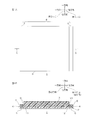
- FIG. 1A to 1B show one embodiment of the low dielectric substrate material of the present invention
- FIG. 1A is a plan view
- FIG. 1B is a sectional view taken along line XX of FIG. 1A
- 2A to 2F are process diagrams illustrating a method for manufacturing and processing the low dielectric substrate material shown in FIG. 1.
- FIG. 2A is a process for preparing a metal layer
- FIG. 2B is a process for forming a first coating film
- 2C is a second step of forming a second coating film
- FIG. 2D is a third step of forming a porous coating film
- a fourth step of forming a spacer layer and a porous resin layer.
- 2E shows a step of pressing the low dielectric substrate material
- FIG. 1A is a plan view
- FIG. 1B is a sectional view taken along line XX of FIG. 1A.
- 2A to 2F are process diagrams illustrating a method for manufacturing and processing the low di
- FIG. 2F shows a step of obtaining the pressed low dielectric substrate material.
- FIG. 3 is a modification example of the low dielectric substrate material shown in FIG. 1A (first spacer members are arranged at one end and the other end of the first margin area in the second direction, respectively, and second spacer members are arranged at the second margin). The top view of the modification which is arrange
- FIG. 4 is a modification example of the low dielectric substrate material shown in FIG. 1A (the first spacer member is arranged at one end of the first margin area in the second direction, and the second spacer member is arranged in the second direction of the second margin area, etc.). The top view of the modification) arrange
- FIG. 3 is a modification example of the low dielectric substrate material shown in FIG. 1A (first spacer members are arranged at one end and the other end of the first margin area in the second direction, respectively, and second spacer members are arranged
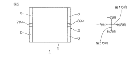
- FIG. 5 is a modification example of the low dielectric substrate material shown in FIG. 1A (the first spacer member is arranged in the middle portion in the second direction of the first margin area, and the second spacer member is arranged in the second direction of the second margin area).
- positioned at the intermediate part) is shown.
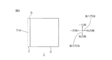
- FIG. 6 is a plan view of a modified example of the low dielectric substrate material shown in FIG. 1A (a modified example in which the spacer layer is composed of the first spacer member that matches the first margin area).
- FIG. 7 is a plan view of a modified example of the low dielectric substrate material shown in FIG. 1A (a modified example in which the spacer layer is a first spacer member arranged at one end of the first margin area in the first direction).
- FIG. 8 shows the measurement points of the dimensions and thickness of the low dielectric substrate material of Example 1.
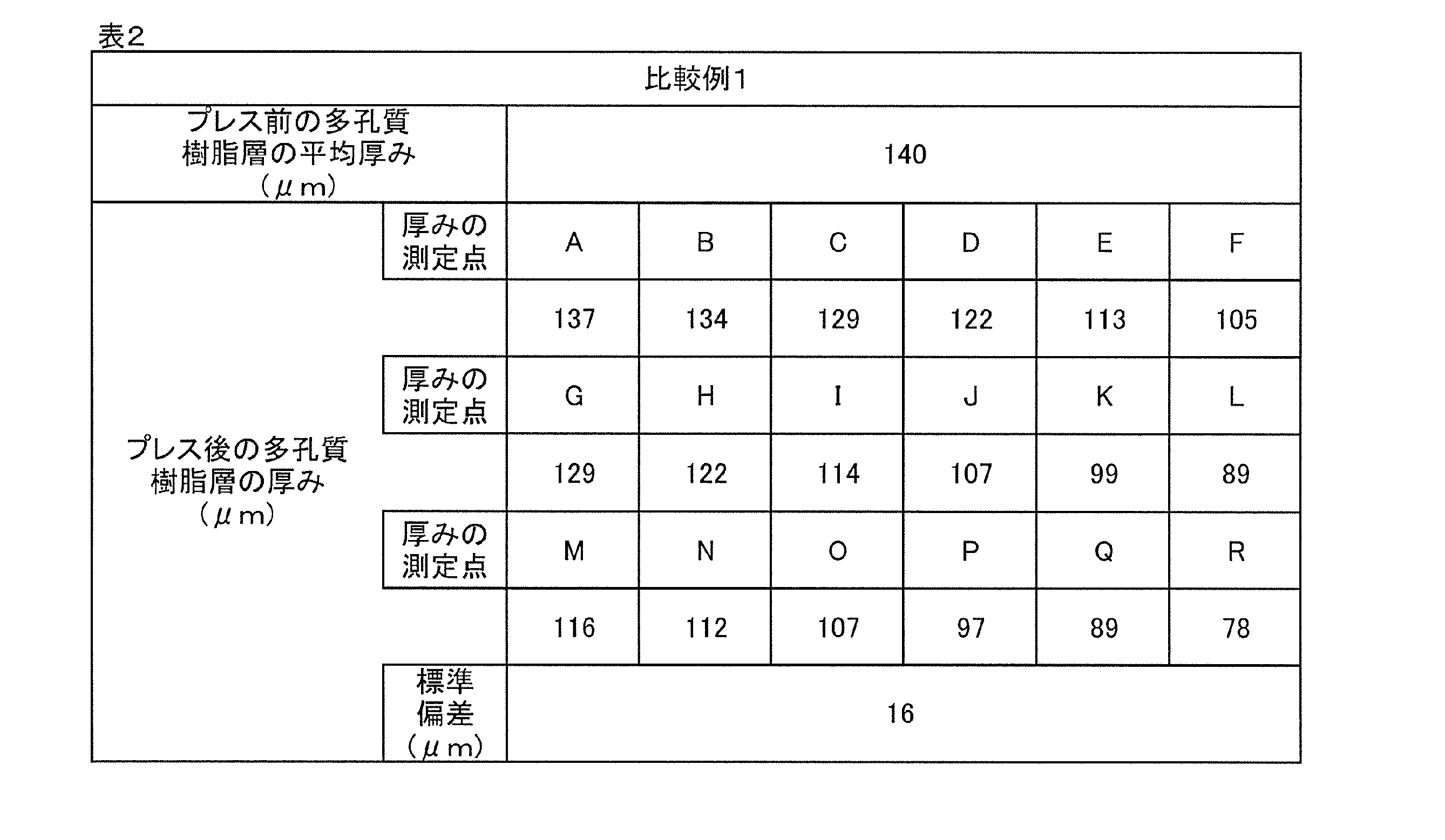
- FIG. 9 shows measurement points of dimensions and thickness of the low dielectric substrate material of Comparative Example 1.
- the low dielectric substrate material 1 has one surface and the other surface facing each other in the thickness direction, and has a sheet shape that spreads in a surface direction orthogonal to the thickness direction.
- the low dielectric substrate material 1 includes a metal layer 2, a porous resin layer 3, and a spacer layer 4.
- the low dielectric substrate material 1 includes only the metal layer 2, the porous resin layer 3, and the spacer layer 4.
- the metal layer 2 has the same outer shape as that of the low dielectric substrate material 1. Specifically, the metal layer 2 has one surface and the other surface facing each other in the thickness direction, and has a sheet shape spreading in the surface direction. Moreover, one surface in the thickness direction of the metal layer 2 is a flat surface. Further, the metal layer 2 forms the other surface in the thickness direction of the low dielectric substrate material 1.
- the metal layer 2 has a substantially rectangular sheet shape, and is arranged at each of one end and the other end in the first direction (the direction corresponding to the left-right direction in FIG. 1A) included in the plane direction. It has a first margin area 5 and a second margin area 6.
- the first margin area 5 and the second margin area 6 are areas where the porous resin layer 3 described below is not arranged.
- the first margin area 5 and the second margin area 6 are spaced from each other in the first direction.
- Each of the first margin area 5 and the second margin area 6 is a substantially strip-shaped area in plan view extending in a second direction (corresponding to the vertical direction in FIG. 1A) orthogonal to the first direction.
- the material of the metal layer 2 is not particularly limited, and examples thereof include metals such as copper, iron, silver, gold, aluminum, nickel, and alloys thereof (stainless steel, bronze). Preferably, copper is used.
- the thickness of the metal layer 2 is, for example, 0.1 ⁇ m or more, preferably 1 ⁇ m or more, and for example, 100 ⁇ m or less, preferably 50 ⁇ m or less.
- the porous resin layer 3 is arranged on one surface of the metal layer 2. Specifically, the porous resin layer 3 is arranged on the one surface of the metal layer 2 between the first margin area 5 and the second margin area 6. The porous resin layer 3 forms one surface of the low dielectric substrate material 1 together with the spacer layer 4 described below.
- the porous resin layer 3 has one surface and the other surface facing each other in the thickness direction, and has a sheet shape that spreads between the first margin area 5 and the second margin area 6 on one surface of the metal layer 2.
- the porous resin layer 3 includes a first outer side surface 9 as an example of a first side surface that connects one edge in the first direction of one side and one edge in the first direction of the other side, and one side in the first direction and the like.
- the second outer side surface 10 as an example of the first side surface that connects the end edge and the other end edge of the other surface in the first direction.
- the one surface in the thickness direction, the other surface, the first outer surface 9 and the second outer surface 10 define a substantially rectangular shape. That is, the porous resin layer 3 has a substantially rectangular shape in the cross section along the first direction.
- the porous resin layer 3 is not particularly limited, and examples thereof include a porous film (preferably a polyimide porous film) described in International Publication No. 2018/186486.
- the porous resin layer 3 has a large number of fine pores (pores).
- the porous resin layer 3 mainly has, for example, a closed cell structure.
- the porosity of the porous resin layer 3 is, for example, 60% or more, preferably 70% or more, more preferably 80% or more, and for example, less than 100%.
- the average diameter of the pores 10 in the porous resin layer 3 (that is, the average pore diameter) is, for example, 10 ⁇ m or less, and for example, 0.1 ⁇ m or more.
- the material of the porous resin layer 3 is not particularly limited, and examples thereof include resins such as thermosetting resins and thermoplastic resins. Preferably, a thermosetting resin is used.
- thermosetting resin examples include polycarbonate resin, thermosetting polyimide resin, thermosetting fluorinated polyimide resin, epoxy resin, phenol resin, urea resin, melamine resin, diallyl phthalate resin, silicone resin, thermosetting urethane resin. , Fluororesins (polymers of fluorinated olefins (specifically, polytetrafluoroethylene (PTFE), etc.)), liquid crystal polymers (LCP), and the like. These can be used alone or in combination of two or more. Preferably, a thermosetting polyimide resin is used.
- the dielectric constant of the porous resin layer 3 at a frequency of 10 GHz is, for example, 3.0 or less, preferably 2.5 or less, more preferably 2.0 or less.
- the thickness of the porous resin layer 3 is, for example, 2 ⁇ m or more, preferably 5 ⁇ m or more, more preferably 25 ⁇ m or more, further preferably 50 ⁇ m or more, particularly preferably 75 ⁇ m or more, and, for example, 1,000 ⁇ m. The following is preferably 500 ⁇ m or less, and more preferably 250 ⁇ m or less.
- the thickness of the porous resin layer 3 is the distance between one surface in the thickness direction of the porous resin layer 3 and one surface in the thickness direction of the metal layer 2.
- the thickness of the porous resin layer 3 is an average thickness in the surface direction.
- the thickness ratio of the porous resin layer 3 is, for example, 1 ⁇ m or more, preferably 5 ⁇ m or more, and for example, 100 ⁇ m or less, more preferably 50 ⁇ m or less, more preferably 20 ⁇ m or less.
- the ratio of the thickness of the porous resin layer 3 to the thickness of the metal layer 2 is, for example, 2 or more, preferably 5 or more, and for example, 100 or less, more preferably 50 or less.
- the spacer layer 4 is a layer extending in the surface direction so that the press of the porous resin layer 3 can be controlled in the press (see FIG. 2E) described later.
- the spacer layer 4 forms one surface in the thickness direction of the low dielectric substrate material 1 together with the porous resin layer 3 described above.
- the spacer layer 4 has a smooth one surface and a smooth other surface facing each other in the thickness direction.
- One surface of the spacer layer 4 is exposed on one side in the thickness direction.
- the other surface of the spacer layer 4 is in contact with the one surface of the metal layer 2.
- the spacer layer 4 is arranged on one surface of the metal layer 2. Specifically, the spacer layer 4 is arranged adjacent to the porous resin layer 3 in the first direction on one surface of the metal layer 2. Specifically, the spacer layer 4 and the porous resin layer 3 are arranged without a gap in the first direction.
- the spacer layer 4 is arranged in the first margin area 5 and the second margin area 6 on one surface of the metal layer 2.
- the spacer layer 4 includes a first spacer member 7 included in the first margin area 5 and a second spacer member 8 included in the second margin area 6 when projected in the thickness direction.
- the first spacer member 7 has a generally rectangular shape in plan view extending in the first direction.
- the first spacer member 7 overlaps with the first margin area 5 when projected in the thickness direction. That is, the entire other surface of the first spacer member 7 is in contact with the entire one surface of the first margin area 5. That is, the first spacer member 7 corresponds to the first margin area 5 in a plan view.
- each of the first direction one end edge, the first direction other end edge, the second direction one end edge, and the second direction other end edge of the first spacer member 7 is a first direction one end edge of the first margin area 5, It coincides with the other edge in the first direction, one edge in the second direction, and the other edge in the second direction.
- the first spacer member 7 has a substantially rectangular shape in a cross-sectional view along the first direction, and is one example of a second side surface that connects one surface, the other surface, and their other ends in the first direction.
- the inner surface 11 is integrally formed.
- the first inner side surface 11 faces the first outer side surface 9 of the porous resin layer 3.
- the first inner side surface 11 contacts the first outer side surface 9.
- the second spacer member 8 has a substantially rectangular shape in plan view extending in the first direction.
- the second spacer member 8 overlaps the second margin area 6 when projected in the thickness direction. That is, the entire other surface of the second spacer member 8 is in contact with the entire one surface of the second margin area 6. That is, the second spacer member 8 coincides with the second margin area 6 in a plan view.
- each of the first direction one edge, the first direction other edge, the second direction one edge, and the second direction other edge of the second spacer member 8 is a first direction one edge of the second margin area 6, It corresponds to each of the other edge in the first direction, one edge in the second direction, and the other edge in the second direction.
- the second spacer member 8 has a substantially rectangular shape in a cross-sectional view along the first direction, and has one surface, the other surface, and a second inner surface as an example of a second side surface that connects the one end edges in the first direction. It has the side surface 12 integrally.
- the second inner side surface 12 faces the second outer side surface 10 of the porous resin layer 3.
- the second inner side surface 12 contacts the second outer side surface 10.
- the spacer layer 4 is not particularly limited as long as the pressing of the porous resin layer 3 can be controlled, and is preferably a non-porous layer. That is, unlike the porous resin layer 3, the spacer layer 4 preferably does not have fine pores (pores) and is formed as a solid dense layer.
- Examples of the material of the spacer layer 4 include the above-mentioned resins such as thermosetting resin and thermoplastic resin.
- the metal exemplified in the metal layer 2 can also be used.
- a resin is preferable, a thermosetting resin is more preferable, and a thermosetting polyimide resin is more preferable.
- the material of the spacer layer 4 is preferably the same resin as the resin exemplified in the porous resin layer 3, more preferably the same thermosetting resin as the thermosetting resin exemplified in the porous resin layer 3. More preferably, the same material as the material of the porous resin layer 3 is used.
- the spacer layer 4 is thinner than the porous resin layer 3. That is, the thickness of the spacer layer 4 is less than the thickness of the porous resin layer 3.
- the value obtained by subtracting the thickness of the spacer layer 4 from the thickness of the porous resin layer 3 is, for example, more than 0 ⁇ m, preferably 1 ⁇ m or more, more preferably 2 ⁇ m or more, further preferably 5 ⁇ m or more, and, for example, It is 50 ⁇ m or less, preferably 25 ⁇ m or less.
- the thickness of the spacer layer 4 is the distance between the one surface in the thickness direction of the spacer layer 4 and the one surface in the thickness direction of the metal layer 2.
- the ratio of the thickness of the spacer layer 4 to the thickness of the porous resin layer 3 is, for example, less than 1 or less, preferably 0.99 or less, more preferably 0.95 or less, and, for example, 0.5 or more. , Preferably 0.6 or more, more preferably 0.7 or more, and further preferably 0.8 or more.
- the thickness of the spacer layer 4 is, for example, 1 ⁇ m or more, preferably 5 ⁇ m or more, more preferably 10 ⁇ m or more, and for example, 100 ⁇ m or less, preferably 50 ⁇ m or less, more preferably 30 ⁇ m or less.
- the thickness of the spacer layer 4 is substantially uniform in the plane direction, that is, the spacer layer 4 has the same thickness in the plane direction.
- the first spacer member 7 since the first spacer member 7 is thinner than the porous resin layer 3, the first spacer member 7 exposes one side portion in the thickness direction of the first outer side surface 9 of the porous resin layer 3 to one side in the first direction. doing. Further, the first inner side surface 11 of the first spacer member 7 is in close contact with the other side portion of the first outer side surface 9 of the porous resin layer 3 in the thickness direction.
- the second spacer member 8 Since the second spacer member 8 is thinner than the porous resin layer 3, the second spacer member 8 exposes one portion in the thickness direction on the second outer side surface 10 side to the other side in the first direction. Further, the second inner side surface 12 of the second spacer member 8 is in close contact with the portion of the second outer side surface 10 of the porous resin layer 3 on the other side in the thickness direction.
- the first direction length of each of the first spacer member 7 and the second spacer member 8 is, for example, 0.1 cm or more, preferably 0.5 cm or more, and for example, 5 cm or less, preferably 2 cm or less. Is.
- the ratio of the first direction length of each of the first spacer member 7 and the second spacer member 8 to the first direction length of the metal layer 2 is, for example, 0.01 or more, preferably 0.02 or more, It is preferably 0.05 or more, and for example, 0.2 or less, preferably 0.1 or less.
- the thickness of the low dielectric substrate material 1 is the total thickness of the metal layer 2 and the porous resin layer 3, and is, for example, 10 ⁇ m or more, preferably 15 ⁇ m or more, more preferably 30 ⁇ m or more. It is not more than 1,000 ⁇ m, preferably not more than 600 ⁇ m, preferably not more than 300 ⁇ m.
- the ratio of the thickness of the metal layer 2 to the thickness of the low dielectric substrate material 1 is, for example, 0.01 or more, preferably 0.05 or more, and for example, 0.75 or less, preferably 0.25 or less. Is.
- the ratio of the thickness of the porous resin layer 3 to the thickness of the low dielectric substrate material 1 is, for example, 0.99 or less, preferably 0.95 or less, and, for example, 0.25 or more, preferably 0. It is 75 or more.
- each member is, for example, in the second direction (paper thickness direction in FIGS. 2A to 2D) by, for example, a roll-to-roll method. It is formed while being conveyed.
- the metal layer 2 is prepared.
- a spacer material preferably a resin
- a spacer material is placed on the first margin area 5 and the second margin area 6 on one surface of the metal layer 2 (implementation of the first step).
- a first varnish containing a resin and a solvent is prepared, and the first varnish is applied (printed) to the first margin area 5 and the second margin area 6 of the metal layer 2 at the same time, and then dried simultaneously to remove the solvent. Are removed to form the first coating film 13.
- the resin is a thermosetting resin
- a first varnish containing the precursor resin is prepared, the first varnish is applied to the first margin area 5 and the second margin area 6 of the metal layer 2, and then Then, the solvent is removed by drying to form the first coating film 13 made of the precursor resin. In this case, the first coating film 13 is still in an uncured state.
- the solvent is not particularly limited, and examples thereof include organic solvents such as N-methyl-2-pyrrolidone (NMP).
- NMP N-methyl-2-pyrrolidone
- the solid content concentration in the first varnish is adjusted to, for example, 10% by mass or more and 50% by mass or less.
- the method for applying the first varnish is not particularly limited, and for example, an applicator or the like that can move (apply) in the second direction relative to the metal layer 2 is used.
- the first coating film 13 is made of a spacer material and has substantially the same shape and dimensions as the spacer layer 4.
- the resin material is arranged between the first margin area 5 and the second margin area 6 on one surface of the first metal layer 3 (implementation of the second step).
- the resin material contains the above-mentioned resin (preferably the same resin as the spacer layer 4), a porosifying agent, and a nucleating agent, and a second varnish containing this resin material and a solvent is prepared.
- the second varnish is applied (printed) between the first margin area 5 and the second margin area 6 on the one surface of the first metal layer 3, and then dried to remove the solvent to remove the second coating film. 14 is formed.
- the method of forming the second coating film 14 can be based on the description in International Publication 2018/186486.
- the second coating film 14 is made of a resin material (a foamable composition containing a resin and a nucleating agent), and has the same plan view shape as the porous resin layer 3.
- the second coating film 14 is, for example, thinner than the first coating film 13, and specifically, the other surface of the second coating film 14 is in contact with one surface of the metal layer 2 while the second coating film 14 is in contact with the first coating film 13.
- One surface of the film 14 is disposed on the other side in the thickness direction than one surface in the thickness direction of the first coating film 13 when projected in the first direction.
- the entire surface of the first outer side surface 9 of the second coating film 14 is in contact with the portion on the other side in the thickness direction of the first inner side surface 11 of the first coating film 13 corresponding to the first spacer member 7. ..
- the entire second outer side surface 10 of the second coating film 14 is in contact with the portion of the second inner side surface 12 of the first coating film 13 corresponding to the second spacer member 8 on the other side in the thickness direction.
- the second coating film 14 is in close contact with the first coating film 13 in the first direction.
- the second coating film 14 is foamed to form the porous coating film 19 (implementation of the third step).
- the foaming method of the second coating film 14 is not particularly limited, and examples thereof include a physical foaming method and a chemical foaming method.
- the physical foaming method include a method in which a porosifying agent, a nucleating agent, etc. are dispersed in a resin, and a bubble is formed by extracting the pouring agent using a supercritical fluid (supercritical extraction method).
- supercritical extraction method examples thereof include a method of dispersing a boiling point liquid (foaming agent) in a resin and then volatilizing the foaming agent to form bubbles (low boiling point liquid volatilization method).
- the supercritical extraction method is described in detail, for example, in International Publication No. 2018/186486.
- the chemical foaming method includes, for example, a method of forming bubbles by a gas generated by thermal decomposition of a compound added to a resin.
- the porous coating film 19 is preferably in a state before complete curing when the resin material contains a thermosetting resin.
- the first coating film 13 and the porous coating film 19 contain a thermosetting resin
- the first coating film 13 and the porous coating film 19 are cured respectively, and the spacer layer 4 and the porous resin layer. 3 are formed respectively (implementation of the fifth step).
- the first coating film 13 and the porous coating film 19 are simultaneously heated.
- thermoset the first coating film 13 containing the thermosetting resin is thermoset.
- thermosetting resin is thermoset.
- the porous resin layer 3 is formed such that the first outer side surface 9 and the second outer side surface 10 thereof are in close contact with the first inner side surface 11 and the second inner side surface 11 of the spacer layer 4, respectively.
- the low dielectric substrate material 1 including the metal layer 2, the porous resin layer 3 and the spacer layer 4 is obtained.
- the thickness of one side of the porous resin layer 3 in the thickness direction is made uniform by pressing.
- a batch method is adopted.
- a flat plate pressing machine 15 including an upper plate 16 and a lower plate 17 is used for pressing the porous resin layer 3.
- the flat plate press 15 may be equipped with a heat source (not shown).
- the other surface in the thickness direction of the upper plate 16 is a flat surface.
- One surface in the thickness direction of the lower plate 17 is a flat surface.
- the other surface of the upper plate 16 and the one surface of the lower plate 17 are substantially parallel to each other.
- the upper plate 16 and the lower plate 17 are relatively movable in the thickness direction while the other surface of the upper plate 16 and one surface of the lower plate 17 are kept substantially parallel to each other.
- the low dielectric substrate material 1 is placed on the flat plate press 15. Specifically, the other surface in the thickness direction of the metal layer 2 is brought into contact with one surface in the thickness direction of the lower plate 17.
- the upper plate 16 is pressed against the low dielectric substrate material 1 in the thickness direction. Specifically, the upper plate 16 is moved to the other side in the thickness direction while the other side in the thickness direction of the upper plate 16 is in contact with the one side in the thickness direction of the low dielectric substrate material 1.
- one surface in the thickness direction of the porous resin layer 3 moves toward the other side in the thickness direction. That is, the porous resin layer 3 is pressed in the thickness direction.
- the pressing of the porous resin layer 3 in the thickness direction is performed such that the upper plate 16 of the flat plate press 15 contacts the spacer layer 4.
- the porous resin layer 3 is pressed by a value obtained by subtracting the thickness of the spacer layer 4 from the thickness of the porous resin layer 3 before pressing.
- the state where the upper plate 16 is in contact with the spacer layer 4 is maintained, for example, for 1 minute or longer, preferably for 5 minutes or longer, more preferably for 15 minutes or longer, and for example, for 60 minutes or shorter. That is, the pressing of the porous resin layer 3 is performed only for the time described above.
- the low dielectric substrate material 1 can be heated together with the above press.
- the heating temperature is, for example, 100° C. or higher, preferably 150° C. or higher, and for example, 210° C. or lower, preferably 195° C. or lower.
- porous resin layer 3 This allows the porous resin layer 3 to have its thickness restored. That is, it is allowed that one surface in the thickness direction of the porous resin layer 3 is arranged above the one surface in the thickness direction of the spacer layer 4.
- the thickness of the porous resin layer 3 after pressing becomes uniform in the surface direction.
- the ratio of the thickness of the porous resin layer 3 after pressing to the thickness of the porous resin layer 3 before pressing is, for example, less than 1, further 0.99 or less, and, for example, 0.5 or more, Furthermore, it is 0.8 or more.
- the low dielectric substrate material 1 is manufactured by the roll-to-roll method, the low dielectric substrate material 1 is cut along the first direction.
- the low dielectric substrate material 1 has a spacer layer 4 thinner than the porous resin layer 3. Therefore, in order to make the thickness of the porous resin layer 3 uniform, if the low dielectric substrate material 1 is pressed in the thickness direction as shown in FIG. While being pressed, it can suppress pressing more than that. Therefore, it is possible to prevent the thickness of the porous resin layer 3 from becoming uneven due to excessive pressing. That is, the spacer layer 4 can control the pressing amount (compression amount) to make the thickness of the porous resin layer 3 uniform.
- the spacer layer 4 opposes the first spacer member 7 and the second spacer member 8 arranged at each of the one end and the other end in the first direction in the first direction.
- the pressing amount in the first direction can be made uniform. Therefore, the thickness of the porous resin layer 3 in the first direction can be made uniform.
- the first spacer member 7 and the second spacer member 8 have a shape extending in the second direction. Therefore, the pressing amount in the second direction can be made uniform. Therefore, the thickness of the porous resin layer 3 in the second direction can be made uniform.
- the spacer layer 4 is a non-porous layer, it is harder than the porous resin layer 3. Therefore, the function of the spacer layer 4 and the uniform pressing of the porous resin layer 3 can be sufficiently exhibited.
- the first outer side surface 9 and the first inner side surface 11 are in close contact with each other, and the second outer side surface 10 and the second inner side surface 12 are in close contact with each other. In doing so, it is possible to prevent the porous resin layer 3 from shifting with respect to the spacer layer 4.
- the porous resin layer 3 and the spacer layer 4 are made of the same material, the adhesion between the first outer side surface 9 and the first inner side surface 11 and the second outer side surface 10 and The adhesion of the second inner side surface 12 can be improved.
- the first step and the fourth step can be sequentially performed, and then the second step, the third step, and the fifth step can be sequentially performed. That is, first, the spacer material is arranged on the metal layer 2 to form the first coating film 13, and subsequently, when the first coating film 13 contains a thermosetting resin, the first coating film 13 is formed. Is heated to form the spacer layer 4 (implementation of the first and fourth steps). After that, the resin material is placed on the metal layer 2 to form the second coating film 14, and then the second coating film 14 is foamed to form the porous coating film 19.
- the porous coating film 19 contains a thermosetting resin
- the porous coating film 19 is heated to form the porous resin layer 3 (implementation of the second, third and fifth steps).
- the second step, the third step, and the fifth step can be sequentially performed, and then the first step and the fourth step can be sequentially performed.
- the first step, the second step, and the third step are sequentially performed, and then the fourth step and the fifth step are sequentially performed.
- the fourth step and the fifth step can be performed by heating with high manufacturing efficiency, and thus can be simultaneously performed, as compared with the method of the modification described above.
- the low dielectric substrate material 1 can be manufactured in a short time.
- a roll press (not shown) can be used instead of the flat plate press 15 in the press shown in FIG. 2E.
- a roll press (not shown) can be used.
- the porous resin layer 3 can be pressed by the roll-to-roll method, so that the manufacturing efficiency is excellent.
- the transport direction in the roll-to-roll method is not particularly limited, and the metal layer 2 can be transported along the first direction, for example.
- the metal layer 2 is conveyed along the second direction.
- each of the first coating film 13 and the second coating film 14 extending in the second direction can be easily applied by the applicator.
- the spacer material is applied (printed) in a pattern corresponding to the first margin area 5 and the second margin area 6 of the metal layer 2 to form the first coating film 13 having the same pattern as that.
- the photosensitive spacer material is first applied to the entire one surface in the thickness direction of the metal layer 2, and then exposed and developed to form the first margin area. It is also possible to pattern the first coating film 13 having a pattern corresponding to 5 and the second margin area 6.
- the first inner side surface 11 is in close contact with the first outer side surface 9 of the porous resin layer 3, but, for example, a gap may be provided between them.
- the second inner side surface 12 is in close contact with the second outer side surface 10 of the porous resin layer 3, but a gap may be provided between them, for example.
- the fourth step and the fifth step are carried out simultaneously, but they can also be carried out separately.
- Each of the first spacer member 7 and the second spacer member 8 has a substantially rectangular shape in a plan view, but the shape thereof is not particularly limited, and may be, for example, a circular shape in a plan view or an elliptical shape in a plan view.
- the first spacer member 7 is arranged at each of the one end portion and the other end portion of the first margin area 5 in the second direction, and the first spacer member 7 is arranged at the second end. Spaced in direction. A second direction intermediate portion of the first margin area 5 is exposed from between the two first spacer members 7.
- the second spacer member 8 is arranged at each of one end and the other end of the second margin area 6 in the second direction, and they are separated from each other in the second direction. A second direction intermediate portion of the second margin area 6 is exposed from between the two second spacer members 8.
- the second spacer member 8 arranged at one end in the second direction of the second margin area 6 and the first spacer member 7 arranged at one end in the second direction of the first margin area 5 have the first
- the porous resin layer 3 is sandwiched in one direction.
- the porous resin layer 3 is sandwiched in the first direction.
- the first spacer member 5 is arranged at each of one end and the other end of the first margin area 7 in the second direction, and the second spacer member 6 is arranged at the second margin area 8. It is arranged at each of one end and the other end in two directions. Therefore, when pressing the porous resin layer 3, the pressing amount in the second direction can be made uniform. Therefore, the thickness of the porous resin layer 3 in the second direction can be made uniform.
- the first spacer member 7 is arranged at one end of the first margin area 5 in the second direction, while the second spacer member 8 is arranged in the second margin area 6 in the second direction. It may be arranged at the end.
- the first spacer member 7 and the second spacer member 8 sandwich the porous resin layer 3 in a direction inclined in the first direction in a plan view.
- the first spacer member 7 is arranged in the second direction intermediate portion (preferably the central portion) of the first margin area 5, while the second spacer member 8 is the second margin area 6 of the second margin area 6. It is arranged in the middle part (preferably the center part) in the direction.
- the first spacer member 7 and the second spacer member 8 sandwich the porous resin layer 3 in the first direction in a plan view.
- the spacer layer 4 can be arranged only in the first margin area 5. Specifically, the spacer layer 4 is composed of only the first spacer member 7.
- the first spacer member 7 overlaps the first margin area 5 when projected in the thickness direction.
- the first spacer member 7 is arranged at one end of the first margin area 5 in the second direction.
- the spacer layer 4 is arranged in both the first margin area 5 and the second margin area 6 as shown in FIGS. 1 and 3 to 5.
- the thickness of the pressed porous resin layer 3 in the first direction can be made uniform.
- the spacer layer 4 may be arranged in a substantially L-shape in plan view on one surface in the thickness direction of the metal layer 2.
- spacer layer 4 in the middle portion of the metal layer 2 in the first direction and to arrange the porous resin layers 3 on both outer sides in the first direction.
- the low dielectric substrate material 1 after pressing is cut along the first direction.
- the low dielectric substrate material 1 before pressing can also be cut along the first direction. ..
- the second coating film 14 is formed thinner than the first coating film 13, but the second coating film 14 may be formed to have the same thickness as the first coating film 13, for example. ..
- the present invention will be described more specifically by showing Examples and Comparative Examples below.
- the present invention is not limited to the examples and comparative examples.
- specific numerical values such as a blending ratio (content ratio), physical property values, and parameters used in the following description are described in the above-mentioned "Description of Embodiments”, and a corresponding blending ratio ( Content ratio), physical property values, parameters, etc. may be replaced with the upper limit (values defined as “below” or “less than”) or the lower limit (value defined as “greater than or equal to” or “exceeded”). it can.
- Example 1 A low dielectric substrate material 1 having the dimensions shown in FIG. 1 and shown in FIG. 8 was manufactured.
- a metal layer 2 made of copper having a length in the first direction of 14 cm, a length in the second direction of 12 cm, and a thickness of 12 ⁇ m was prepared.
- the polyimide precursor [BPDA/PDA, DPE] (P-phenylenediamine/diaminodiphenyl ether, biphenyltetracarboxylic acid dihydrate) described in Reference Example of WO2018/186486 and NMP are contained.
- 2B solid concentration 20% by mass
- the varnish is applied to the first margin area 5 and the second margin area 6 by the width ( A first direction length of 1 cm) was applied at the same time, and then simultaneously dried to form a 125 ⁇ m-thick first coating film 13 made of a thermosetting polyimide precursor (implementation of the first step).
- a second varnish described in Example 1 of WO2018/186486 (20% by mass of solid content) was prepared, and as shown in FIG. 2C, the second varnish was applied to the first coating film 13 by an applicator.
- the second coating film 14 made of a thermosetting polyimide precursor having a thickness of 10 ⁇ m was formed by applying on one surface of the metal layer 2 in between and then drying (implementation of the second step).
- the porosifying agent was extracted from the second coating film 14 using supercritical carbon dioxide, and the second coating film 14 was foamed to form the porous coating film 19 (supercritical extraction method) (third method). Implementation of the process).
- the first coating film 13 and the porous coating film 19 were simultaneously heated under vacuum at 380° C. for 2 hours. Thereby, as shown in FIG. 2D, each of the first coating film 13 and the porous coating film 19 was cured to form the spacer layer 4 and the porous resin layer 3 (implementation of the fourth step and the fifth step). ).
- the porous resin layer 3 was thicker than the spacer layer 4, and the average thickness was 140 ⁇ m.
- the low dielectric substrate material 1 including the metal layer 2, the porous resin layer 3 and the spacer layer 4 was manufactured.
- the low dielectric substrate material 1 was pressed in the thickness direction by the flat plate press 15.
- the pressing pressure was 5 MPa
- the pressing temperature was 180° C.
- the pressing time was 30 minutes.
- the low dielectric substrate material 1 was taken out from the flat plate press 15.
- the thickness of the porous resin layer 3 at the measurement points A to R shown in FIG. 8 was calculated using a thickness meter. Then, their standard deviations were calculated. The standard deviation indicates the degree of variation in the surface direction of the porous resin layer 3, and the low value of the standard deviation indicates that the thickness is uniform. The results are shown in Table 1.
- Comparative Example 1 Except that the first coating film 13 and the spacer layer 4 were not formed, the same process as in Example 1 was carried out to manufacture the low dielectric substrate material 1 shown in FIG.
- the low dielectric substrate material of the present invention is used, for example, as a film for a millimeter wave antenna capable of long-distance wireless communication.
- Second Spacer Member 9 First Outer Surface (One Example of First Side Surface) 10 2nd outer side surface (an example of 1st side surface) 11 1st inner side surface (an example of 2nd side surface) 12 Second inner side surface (an example of the second side surface) 13 First coating film 14 Second coating film 19 Porous coating film
Landscapes
- Life Sciences & Earth Sciences (AREA)
- Engineering & Computer Science (AREA)
- Wood Science & Technology (AREA)
- Laminated Bodies (AREA)
Abstract
低誘電基板材(1)は、金属層(2)と、金属層(2)の厚み方向一方面に配置される多孔質樹脂層(3)と、金属層(2)の一方面に、多孔質樹脂層(3)に隣接するように配置され、多孔質樹脂層(3)より薄いスペーサ層(4)とを備える。
Description
本発明は、低誘電基板材およびその製造方法に関する。
近年、低誘電性のポリマーフィルムは、長距離無線通信が可能なミリ波アンテナ用フィルムとして有用であることが知られている。
例えば、銅箔と、その上に形成され、空孔率が60%以上、平均孔径が50μm以下である空孔を有するポリイミド多孔フィルムとを備える積層体が提案されている(例えば、下記特許文献1参照。)。この積層体を製造するには、銅箔を準備し、銅箔上にポリイミド前駆体層を形成し、その後、ポリイミド前駆体層を発泡および硬化して、ポリイミド多孔フィルムを作製する。
しかるに、銅箔から回路を形成する回路形成工程おいて、積層体を平板プレス機によってプレスすると、ポリイミド多孔フィルムの厚みにばらつきが発生する。そのため、回路内の箇所によって誘電率が異なり、その結果、回路内で特性インピーダンスが不均一となる。そうすると、回路に流れる信号電流の一部が反射されてノイズとなったり、出力が低下する不具合がある。
本発明は、上記課題を解決するため、多孔質樹脂層の厚みを均一にすることができる低誘電基板材およびその製造方法を提供する。
本発明(1)は、金属層と、前記金属層の厚み方向一方面に配置される多孔質樹脂層と、前記金属層の前記一方面に、前記多孔質樹脂層に隣接するように配置され、前記多孔質樹脂層より薄いスペーサ層とを備える、低誘電基板材を含む。
この低誘電基板材は、多孔質樹脂層より薄いスペーサ層を備える。そのため、この低誘電基板材を厚み方向にプレスすれば、多孔質樹脂層は、スペーサ層の厚みまでは、プレスされる一方、それを上回るプレスを抑制できる。そのため、過度のプレスに起因して多孔質樹脂層の厚みが不均一となることを抑制することができる。つまり、スペーサ層によって、プレス量(圧縮量)を制御して、多孔質樹脂層の厚みを均一にすることができる。
本発明(2)は、前記金属層は、前記厚み方向に直交する面方向に含まれる第1方向における一端部および他端部のそれぞれに配置される第1マージンエリアおよび第2マージンエリアであって、前記面方向に含まれ、前記第1方向に直交する第2方向に延びる前記第1マージンエリアおよび前記第2マージンエリアを有し、前記スペーサ層は、厚み方向に投影したときに、前記第1マージンエリアに含まれる第1スペーサ部材と、前記第2マージンエリアに含まれる第2スペーサ部材とを備える、(1)に記載の低誘電基板材を含む。
この低誘電基板材では、スペーサは、第1方向における一端部および他端部のそれぞれに配置される第1スペーサ部材と第2スペーサ部材とを備えるので、第1方向におけるプレス量を均一にすることができる。そのため、第1方向における多孔質樹脂層の厚みを均一にすることができる。
本発明(3)は、前記第1スペーサ部材および前記第2スペーサ部材は、前記第2方向に延びる形状を有する、(2)に記載の低誘電基板材を含む。
この低誘電基板材では、第1スペーサ部材および第2スペーサ部材は、第2方向に延びる形状を有する。そのため、第2方向における多孔質樹脂層の厚みを均一にすることができる。
本発明(4)は、前記第1スペーサ部材は、前記第1マージンエリアの前記第2方向一端部および他端部のそれぞれに配置されており、それらは、前記第2方向において間隔が隔てられ、前記第2スペーサ部材は、前記第2マージンエリアの前記第2方向一端部および他端部のそれぞれに配置されており、それらは、前記第2方向において間隔が隔てられる、(2)に記載の低誘電基板材を含む。
この低誘電基板材では、第1スペーサ部材が、第1マージンエリアの第2方向一端部および他端部のそれぞれに配置され、第2スペーサ部材が、第2マージンエリアの第2方向一端部および他端部のそれぞれに配置されている。そのため、第2方向におけるプレス量を均一にすることができる。そのため、第2方向における多孔質樹脂層の厚みを均一にすることができる。
本発明(5)は、前記スペーサ層は、無孔質層である、(1)~(4)のいずれか一項に記載の低誘電基板材を含む。
この低誘電基板材では、スペーサ層は、無孔質層であるので、多孔質樹脂層より硬い。
そのため、スペーサ層の機能を十分に発揮することができる。
そのため、スペーサ層の機能を十分に発揮することができる。
本発明(6)は、前記多孔質樹脂層は、前記スペーサ層に面する第1側面を有し、前記スペーサ層は、前記多孔質樹脂層に面する第2側面を有し、前記第1側面および前記第2側面が、密着している、(1)~(5)のいずれか一項に記載の低誘電基板材を含む。
この低誘電基板材では、第1側面および第2側面が、密着しているので、低誘電基板材をプレスする際に、多孔質樹脂層がスペーサ層に対してずれることを抑制することができる。
本発明(7)は、前記多孔質樹脂層および前記スペーサ層は、同一の材料からなる、(6)のいずれか一項に記載の低誘電基板材を含む。
この低誘電基板材では、多孔質樹脂層およびスペーサ層は、同一の材料からなるので、第1側面および前記第2側面の密着力を向上できる。
本発明(8)は、(1)~(7)のいずれか一項に記載の低誘電基板材を製造する方法であり、前記金属層の前記一方面にスペーサ材料を塗布して、第1塗膜を形成する第1工程と、前記金属層の前記一方面に、前記スペーサ材料に隣接するように、樹脂材料を塗布して、第2塗膜を形成する第2工程と、前記第2塗膜を発泡させて、多孔質塗膜を形成する第3工程と、前記第1塗膜を硬化させて、前記スペーサ層を形成する第4工程と、前記多孔質塗膜を硬化させて、前記多孔質樹脂層を形成する第5工程とを備え、低誘電基板材の製造方法を含む。
この方法では、第1工程、第2工程および第3工程を順に実施し、第4工程および第5工程を順に実施できる。そのため、この方法では、第1工程および第4工程を順に実施してから、第2工程、第3工程および第5工程を順に実施する方法や、第2工程、第3工程および第5工程を順に実施してから、第1工程および第4工程を順に実施する方法に比べて、第4工程および第5工程を製造効率よく実施することができる。
本発明(9)は、前記第4工程および前記第5工程を同時に実施する、(8)に記載の低誘電基板材の製造方法を含む。
この製造方法では、第4工程および第5工程を同時に実施するので、低誘電基板材を短時間で製造することができる。
本発明の低誘電基板材によれば、スペーサ層によって、プレス量(圧縮量)を制御して、多孔質樹脂層の厚みを均一にすることができる。
本発明の低誘電基板材の製造方法によれば、第4工程および第5工程を製造効率よく実施することができる。
<一実施形態>
本発明の低誘電基板材の一実施形態を、図1A~図1Bを参照して説明する。
本発明の低誘電基板材の一実施形態を、図1A~図1Bを参照して説明する。
低誘電基板材1は、厚み方向に対向する一方面および他方面を有し、厚み方向に直交する面方向に広がるシート形状を有する。低誘電基板材1は、金属層2と、多孔質樹脂層3と、スペーサ層4とを備える。好ましくは、低誘電基板材1は、金属層2と、多孔質樹脂層3と、スペーサ層4とのみを備える。
金属層2は、低誘電基板材1の外形形状と同一の外形形状を有する。具体的には、金属層2は、厚み方向に対向する一方面および他方面を有し、面方向に広がるシート形状を有する。また、金属層2の厚み方向一方面は、平坦面である。また、金属層2は、低誘電基板材1の厚み方向他方面を形成する。
より具体的には、金属層2は、略矩形シート形状をなしており、面方向に含まれる第1方向(図1Aにおける左右方向に相当する方向)における一端部および他端部のそれぞれに配置される第1マージンエリア5および第2マージンエリア6を有する。
第1マージンエリア5および第2マージンエリア6は、次に説明する多孔質樹脂層3が配置されないエリアである。第1マージンエリア5および第2マージンエリア6は、第1方向おいて互いに間隔が隔てられている。第1マージンエリア5および第2マージンエリア6のそれぞれは、第1方向に直交する第2方向(図1Aにおける上下方向に相当)に延びる平面視略帯状のエリアである。
金属層2の材料は、特に限定されず、例えば、銅、鉄、銀、金、アルミニウム、ニッケル、それらの合金(ステンレス、青銅)などの金属が挙げられる。好ましくは、銅が挙げられる。
金属層2の厚みは、例えば、0.1μm以上、好ましくは、1μm以上であり、また、例えば、100μm以下、好ましくは、50μm以下である。
多孔質樹脂層3は、金属層2の一方面に配置されている。具体的には、多孔質樹脂層3は金属層2の一方面において、第1マージンエリア5および第2マージンエリア6の間に配置されている。多孔質樹脂層3は、次に説明するスペーサ層4とともに、低誘電基板材1の一方面を形成する。
多孔質樹脂層3は、厚み方向に対向する一方面および他方面を有し、金属層2の一方面の第1マージンエリア5および第2マージンエリア6の間に広がるシート形状を有する。
また、多孔質樹脂層3は、一方面の第1方向一端縁および他方面の第1方向一端縁を連結する第1側面の一例としての第1外側面9と、一方面の第1方向他端縁および他方面の第1方向他端縁を連結する第1側面の一例としての第2外側面10とを備える。これにより、厚み方向一方面、他方面、第1外側面9および第2外側面10は、略矩形状を区画する。つまり、多孔質樹脂層3は、第1方向に沿う断面において、略矩形状を有する。
また、多孔質樹脂層3は、一方面の第1方向一端縁および他方面の第1方向一端縁を連結する第1側面の一例としての第1外側面9と、一方面の第1方向他端縁および他方面の第1方向他端縁を連結する第1側面の一例としての第2外側面10とを備える。これにより、厚み方向一方面、他方面、第1外側面9および第2外側面10は、略矩形状を区画する。つまり、多孔質樹脂層3は、第1方向に沿う断面において、略矩形状を有する。
多孔質樹脂層3は、特に限定されず、例えば、国際公開2018/186486号公報などに記載される多孔質フィルム(好ましくは、ポリイミド多孔フィルム)などが挙げられる。
また、多孔質樹脂層3は、微細な空孔(気孔)を多数有している。多孔質樹脂層3は、例えば、独立気泡構造を主として有する。
多孔質樹脂層3における空孔率は、例えば、60%以上、好ましくは、70%以上、より好ましくは、80%以上であり、また、例えば、100%未満である。
多孔質樹脂層3における空孔10の平均径(つまり、平均孔径)は、例えば、10μm以下であり、また、例えば、0.1μm以上である。
多孔質樹脂層3の材料(樹脂材料の一例)としては、特に限定されず、例えば、熱硬化性樹脂、熱可塑性樹脂などの樹脂が挙げられる。好ましくは、熱硬化性樹脂が挙げられる。
熱硬化性樹脂としては、例えば、ポリカーボネート樹脂、熱硬化性ポリイミド樹脂、熱硬化性フッ化ポリイミド樹脂、エポキシ樹脂、フェノール樹脂、ユリア樹脂、メラミン樹脂、ジアリルフタレート樹脂、シリコーン樹脂、熱硬化性ウレタン樹脂、フッ素樹脂(含フッ素オレフィンの重合体(具体的には、ポリテトラフルオロエチレン(PTFE)など))、液晶ポリマー(LCP)などが挙げられる。これらは、単独使用または2種以上併用することができる。好ましくは、熱硬化性ポリイミド樹脂が挙げられる。
多孔質樹脂層3の周波数10GHzにおける誘電率は、例えば、3.0以下、好ましくは、2.5以下、より好ましくは、2.0以下である。
多孔質樹脂層3の厚みは、例えば、2μm以上、好ましくは、5μm以上、より好ましくは、25μm以上、さらに好ましくは、50μm以上、とりわけ好ましくは、75μm以上であり、また、例えば、1,000μm以下、好ましくは、500μm以下、好ましくは、250μm以下である。多孔質樹脂層3の厚みは、多孔質樹脂層3の厚み方向一方面と、金属層2の厚み方向一方面との間の距離である。また、多孔質樹脂層3の厚みは、面方向における平均厚みである。
また、多孔質樹脂層3の厚みの割合は、例えば、1μm以上、好ましくは、5μm以上であり、また、例えば、100μm以下、より好ましくは、50μm以下、より好ましくは、20μm以下である。
また、金属層2の厚みに対する多孔質樹脂層3の厚みの割合は、例えば、2以上、好ましくは、5以上であり、また、例えば、100以下、より好ましくは、50以下である。
スペーサ層4は、後述するプレス(図2E参照)において、多孔質樹脂層3のプレスを制御できるように構成される面方向に延びる層である。
スペーサ層4は、上記した多孔質樹脂層3とともに、低誘電基板材1の厚み方向一方面を形成する。スペーサ層4は、厚み方向に対向する平滑な一方面および平滑な他方面を備える。スペーサ層4の一方面は、厚み方向一方側に露出している。スペーサ層4の他方面は、金属層2の一方面に接触している。
スペーサ層4は、金属層2の一方面に配置されている。具体的には、スペーサ層4は、金属層2の一方面において、多孔質樹脂層3と第1方向に隣接配置されている。詳しくは、スペーサ層4は、多孔質樹脂層3と、第1方向において隙間なく配置されている。
具体的には、スペーサ層4は、金属層2の一方面における第1マージンエリア5および第2マージンエリア6に配置されている。スペーサ層4は、厚み方向に投影したときに、第1マージンエリア5に含まれる第1スペーサ部材7と、第2マージンエリア6に含まれる第2スペーサ部材8とを備える。
第1スペーサ部材7は、第1方向に延びる平面視略矩形状を有する。第1スペーサ部材7は、厚み方向に投影したときに、第1マージンエリア5と互いに重複する。つまり、第1スペーサ部材7の他方面全面は、第1マージンエリア5の一方面全面に接触している。
すなわち、第1スペーサ部材7は、平面視において、第1マージンエリア5に一致している。詳しくは、第1スペーサ部材7の第1方向一端縁、第1方向他端縁、第2方向一端縁および第2方向他端縁のそれぞれは、第1マージンエリア5の第1方向一端縁、第1方向他端縁、第2方向一端縁および第2方向他端縁のそれぞれに一致する。第1スペーサ部材7は、第1方向に沿う断面視で、略矩形状を有し、一方面、他方面、およびそれらの第1方向他端縁を連結する第2側面の一例としての第1内側面11を一体的に有する。第1内側面11は、多孔質樹脂層3の第1外側面9に面する。第1内側面11は、第1外側面9に接触する。
すなわち、第1スペーサ部材7は、平面視において、第1マージンエリア5に一致している。詳しくは、第1スペーサ部材7の第1方向一端縁、第1方向他端縁、第2方向一端縁および第2方向他端縁のそれぞれは、第1マージンエリア5の第1方向一端縁、第1方向他端縁、第2方向一端縁および第2方向他端縁のそれぞれに一致する。第1スペーサ部材7は、第1方向に沿う断面視で、略矩形状を有し、一方面、他方面、およびそれらの第1方向他端縁を連結する第2側面の一例としての第1内側面11を一体的に有する。第1内側面11は、多孔質樹脂層3の第1外側面9に面する。第1内側面11は、第1外側面9に接触する。
第2スペーサ部材8は、第1方向に延びる平面視略矩形状を有する。第2スペーサ部材8は、厚み方向に投影したときに、第2マージンエリア6と互いに重複する。つまり、第2スペーサ部材8の他方面全面は、第2マージンエリア6の一方面全面に接触している。
すなわち、第2スペーサ部材8は、平面視において、第2マージンエリア6に一致している。詳しくは、第2スペーサ部材8の第1方向一端縁、第1方向他端縁、第2方向一端縁および第2方向他端縁のそれぞれは、第2マージンエリア6の第1方向一端縁、第1方向他端縁、第2方向一端縁および第2方向他端縁のそれぞれに一致する。第2スペーサ部材8は、第1方向に沿う断面視で、略矩形状を有し、一方面、他方面、およびそれらの第1方向一端縁を連結する第2側面の一例としての第2内側面12を一体的に有する。第2内側面12は、多孔質樹脂層3の第2外側面10に面する。第2内側面12は、第2外側面10に接触する。
すなわち、第2スペーサ部材8は、平面視において、第2マージンエリア6に一致している。詳しくは、第2スペーサ部材8の第1方向一端縁、第1方向他端縁、第2方向一端縁および第2方向他端縁のそれぞれは、第2マージンエリア6の第1方向一端縁、第1方向他端縁、第2方向一端縁および第2方向他端縁のそれぞれに一致する。第2スペーサ部材8は、第1方向に沿う断面視で、略矩形状を有し、一方面、他方面、およびそれらの第1方向一端縁を連結する第2側面の一例としての第2内側面12を一体的に有する。第2内側面12は、多孔質樹脂層3の第2外側面10に面する。第2内側面12は、第2外側面10に接触する。
スペーサ層4は、多孔質樹脂層3のプレスを制御できれば特に限定されず、好ましくは、無孔質層である。つまり、スペーサ層4は、好ましくは、多孔質樹脂層3と異なり、微細な空孔(気孔)を有さず、中実な緻密層として形成されている。
スペーサ層4の材料(スペーサ材料の一例)としては、例えば、上記した熱硬化性樹脂、熱可塑性樹脂などの樹脂が挙げられる。また、スペーサ層4の材料として、金属層2で例示した金属も挙げられる。スペーサ層4の材料として、好ましくは、樹脂、より好ましくは、熱硬化性樹脂、さらに好ましくは、熱硬化性ポリイミド樹脂が挙げられる。
また、スペーサ層4の材料として、好ましくは、多孔質樹脂層3で例示した樹脂と同一の樹脂、より好ましくは、多孔質樹脂層3で例示した熱硬化性樹脂と同一の熱硬化性樹脂が挙げられ、さらに好ましくは、多孔質樹脂層3の材料と同一の材料が挙げられる。
スペーサ層4は、多孔質樹脂層3より薄い。つまり、スペーサ層4の厚みは、多孔質樹脂層3の厚み未満である。
多孔質樹脂層3の厚みからスペーサ層4の厚みを差し引いた値は、例えば、0μm超過、好ましくは、1μm以上、より好ましくは、2μm以上、さらに好ましくは、5μm以上であり、また、例えば、50μm以下、好ましくは、25μm以下である。
スペーサ層4の厚みは、スペーサ層4の厚み方向一方面と、金属層2の厚み方向一方面との間の距離である。
多孔質樹脂層3の厚みに対するスペーサ層4の厚みの割合は、例えば、1未満以下、好ましくは、0.99以下、より好ましくは、0.95以下であり、また、例えば、0.5以上、好ましくは、0.6以上、より好ましくは、0.7以上、さらに好ましくは、0.8以上である。
スペーサ層4の厚みは、例えば、1μm以上、好ましくは、5μm以上、より好ましくは、10μm以上であり、また、例えば、100μm以下、好ましくは、50μm以下、より好ましくは、30μm以下である。
なお、スペーサ層4の厚みは、面方向において実質的に均一であり、つまり、スペーサ層4は、面方向において同一厚みを有する。
また、第1スペーサ部材7が多孔質樹脂層3より薄いことから、第1スペーサ部材7は、多孔質樹脂層3の第1外側面9の厚み方向一方側部分を第1方向一方側に露出している。また、第1スペーサ部材7の第1内側面11は、多孔質樹脂層3の第1外側面9の厚み方向他方側部分と密着している。
第2スペーサ部材8が多孔質樹脂層3より薄いことから、第2スペーサ部材8は、第2外側面10側の厚み方向一方側部分を第1方向他方側に露出している。また、第2スペーサ部材8の第2内側面12は、多孔質樹脂層3の第2外側面10の厚み方向他方側部分と密着している。
第1スペーサ部材7および第2スペーサ部材8のそれぞれの第1方向長さは、例えば、0.1cm以上、好ましくは、0.5cm以上であり、また、例えば、5cm以下、好ましくは、2cm以下である。
金属層2の第1方向長さに対する、第1スペーサ部材7および第2スペーサ部材8のそれぞれの第1方向長さの割合は、例えば、0.01以上、好ましくは、0.02以上、より好ましくは、0.05以上であり、また、例えば、0.2以下、好ましくは、0.1以下である。
低誘電基板材1の厚みは、金属層2および多孔質樹脂層3の総厚みであって、例えば、10μm以上、好ましくは、15μm以上、より好ましくは、30μm以上であり、また、例えば、1,000μm以下、好ましくは、600μm以下、好ましくは、300μm以下である。
低誘電基板材1の厚みに対する金属層2の厚みの割合は、例えば、0.01以上、好ましくは、0.05以上であり、また、例えば、0.75以下、好ましくは、0.25以下である。
低誘電基板材1の厚みに対する多孔質樹脂層3の厚みの割合は、例えば、0.99以下、好ましくは、0.95以下であり、また、例えば、0.25以上、好ましくは、0.75以上である。
次に、低誘電基板材1の製造方法および加工方法を、図2A~図2Fを参照して、説明する。
なお、一実施形態における低誘電基板材1の製造(図2A~図2D)では、例えば、ロールトゥロール法によって、各部材を、例えば、第2方向(図2A~図2Dにおける紙厚方向)に搬送しながら形成する。
図2Aに示すように、まず、金属層2を準備する。
図2Bに示すように、次いで、スペーサ材料(好ましくは、樹脂)を金属層2の一方面の第1マージンエリア5および第2マージンエリア6に配置する(第1工程の実施)。好ましくは、樹脂および溶媒を含有する第1ワニスを調製し、第1ワニスを金属層2の第1マージンエリア5および第2マージンエリア6に同時に塗布(印刷)し、その後、同時に乾燥して溶媒を除去して、第1塗膜13を形成する。
樹脂が熱硬化性樹脂である場合には、その前駆体樹脂を含有する第1ワニスを調製し、第1ワニスを金属層2の第1マージンエリア5および第2マージンエリア6に塗布し、その後、乾燥して溶媒を除去して、前駆体樹脂からなる第1塗膜13を形成する。この場合には、第1塗膜13は、まだ未硬化状態である。
溶媒は、特に限定されず、例えば、N-メチル-2-ピロリドン(NMP)などの有機溶媒が挙げられる。第1ワニスにおける固形分濃度は、例えば、10質量%以上、50質量%以下に調整される。第1ワニスの塗布方法は、特に限定されず、例えば、金属層2に対して第2方向に相対移動(塗布)可能なアプリケータなどが用いられる。
第1塗膜13は、スペーサ材料からなっており、スペーサ層4と実質的に同一の形状および寸法を有する。
図2Cに示すように、次いで、樹脂材料を第1金属層3の一方面における第1マージンエリア5および第2マージンエリア6の間に配置する(第2工程の実施)。樹脂材料は、上記した樹脂(好ましくは、スペーサ層4と同一の樹脂)と、多孔化剤と、核剤とを含んでおり、この樹脂材料および溶媒を含む第2ワニスを調製する。次いで、第2ワニスを、第1金属層3の一方面における第1マージンエリア5および第2マージンエリア6の間に塗布(印刷)し、その後、乾燥して溶媒を除去して第2塗膜14を形成する。
第2塗膜14の形成方法等は、国際公開2018/186486号公報などの記載に準拠できる。
第2塗膜14は、樹脂材料(樹脂および核剤を含有する発泡性組成物)からなっており、多孔質樹脂層3と同一の平面視形状を有する。
なお、第2塗膜14は、例えば、第1塗膜13より薄く、具体的には、第2塗膜14の他方面は、金属層2の一方面に接触している一方、第2塗膜14の一方面は、第1方向に投影したときに、第1塗膜13の厚み方向一方面より、厚み方向他方側に配置されている。具体的には、第2塗膜14の第1外側面9の全面は、第1スペーサ部材7に対応する第1塗膜13の第1内側面11の厚み方向他方側部分に接触している。第2塗膜14の第2外側面10の全面は、第2スペーサ部材8に対応する第1塗膜13の第2内側面12の厚み方向他方側部分に接触している。
第2塗膜14は、第1塗膜13に対して、第1方向において密着状に隣接する。
その後、図2Dに示すように、第2塗膜14を発泡させて、多孔質塗膜19を形成する(第3工程の実施)。
第2塗膜14の発泡方法は、特に限定されず、例えば、物理的発泡方法や化学的発泡方法が挙げられる。物理的発泡方法としては、例えば、多孔化剤および核剤等を樹脂に分散させ、超臨界流体を用いて多孔化剤を抽出することにより気泡を形成させる方法(超臨界抽出法)や、低沸点液体(発泡剤)を樹脂に分散させ、次いで、発泡剤を揮発させて、気泡を形成させる方法(低沸点液体揮発法)などが挙げられる。なお、超臨界抽出法は、例えば、国際公開2018/186486号公報などに詳述される。
化学的発泡方法としては、例えば、樹脂に添加した化合物の熱分解により生じたガスにより気泡を形成させる方法などが挙げられる。
なお多孔質塗膜19は、樹脂材料が熱硬化性樹脂を含有する場合には、好ましくは、完全硬化前の状態である。
その後、第1塗膜13および多孔質塗膜19が熱硬化性樹脂を含有する場合には、第1塗膜13および多孔質塗膜19をそれぞれ硬化させて、スペーサ層4および多孔質樹脂層3をそれぞれ形成する(第5工程の実施)。
具体的には、第1塗膜13および多孔質塗膜19を同時に加熱する。
これにより、熱硬化性樹脂を含有する第1塗膜13は、熱硬化する。
一方、熱硬化性樹脂を含有する多孔質塗膜19は、熱硬化する。
これにより、スペーサ層4および多孔質樹脂層3が形成される。多孔質樹脂層3は、その第1外側面9および第2外側面10のそれぞれがスペーサ層4の第1内側面11および第2内側面11のそれぞれと密着した状態で、形成される。
これにより、金属層2、多孔質樹脂層3およびスペーサ層4を備える低誘電基板材1を得る。
その後、多孔質樹脂層3の厚み方向一方面をプレスにより厚みを均一にする。なお、この加工は、例えば、バッチ方式が採用される。
図2Eに示すように、多孔質樹脂層3のプレスには、例えば、上板16および下板17を備える平板プレス機15が用いられる。なお、平板プレス機15には、図示しない熱源を備えることもできる。上板16の厚み方向他方面は、平坦面である。下板17の厚み方向一方面は、平坦面である。上板16の他方面と、下板17の一方面とは、略平行である。具体的には、上板16の他方面と、下板17の一方面とが略平行を保った状態で、上板16および下板17が厚み方向に相対移動可能である。
まず、低誘電基板材1を平板プレス機15に配置する。具体的には、金属層2の厚み方向他方面を、下板17の厚み方向一方面に接触させる。
図2Eに示すように、次いで、上板16を低誘電基板材1に対して厚み方向にプレスする。具体的には、上板16の厚み方向他方面を、低誘電基板材1の厚み方向一方面に接触させながら、上板16を厚み方向他方側に移動させる。
これにより、まず、多孔質樹脂層3の厚み方向一方面が厚み方向他方側に向けて移動する。つまり、多孔質樹脂層3が厚み方向にプレスされる。
続いて、上板16の厚み方向他方面がスペーサ層4の厚み方向一方面に接触すると、上板16の厚み方向他方面の厚み方向他方側への移動が規制されて、多孔質樹脂層3のプレスがそれ以上進行しない。
つまり、多孔質樹脂層3の厚み方向のプレスは、平板プレス機15の上板16がスペーサ層4に接触するように、実施される。具体的には、プレス前の多孔質樹脂層3の厚みから、スペーサ層4の厚みを差し引いた値分だけ、多孔質樹脂層3がプレスされる。
続いて、上板16がスペーサ層4に接触した状態を、例えば、1分以上、好ましくは、5分以上、より好ましくは、15分以上、また、例えば、60分以下、維持する。つまり、上記した時間だけ、多孔質樹脂層3のプレスが実施される。
また、上記プレスとともに、低誘電基板材1を加熱することもできる。加熱温度は、例えば、100℃以上、好ましくは、150℃以上であり、また、例えば、210℃以下、好ましくは、195℃以下である。
その後、図2Fに示すように、平板プレス機15によるプレスを解放する。
これにより、多孔質樹脂層3は、その厚みが復元することが許容される。つまり、多孔質樹脂層3の厚み方向一方面が、スペーサ層4の厚み方向一方面に対して、上側に配置されることが許容される。
そして、プレス後の多孔質樹脂層3の厚みは、面方向に均一となる。
プレス前の多孔質樹脂層3の厚みに対する、プレス後の多孔質樹脂層3の厚みの比は、例えば、1未満、さらには、0.99以下であり、また、例えば、0.5以上、さらには、0.8以上である。
その後、必要により、低誘電基板材1がロールトゥロール法により製造されていれば、第1方向に沿って低誘電基板材1を切断加工する。
そして、この低誘電基板材1は、多孔質樹脂層3より薄いスペーサ層4を備える。そのため、多孔質樹脂層3の厚みを均一にするために、図2Eに示すように、低誘電基板材1を厚み方向にプレスすれば、多孔質樹脂層3は、スペーサ層4の厚みまではプレスされる一方、それを上回るをプレスを抑制できる。そのため、過度のプレスに起因して多孔質樹脂層3の厚みが不均一となることを抑制することができる。つまり、スペーサ層4によって、プレス量(圧縮量)を制御して、多孔質樹脂層3の厚みを均一にすることができる。
また、この低誘電基板材1では、スペーサ層4が、第1方向における一端部および他端部のそれぞれに配置される第1スペーサ部材7と第2スペーサ部材8とを第1方向に対向するように備えるので、第1方向におけるプレス量を均一にすることができる。そのため、第1方向における多孔質樹脂層3の厚みを均一にすることができる。
さらに、この低誘電基板材1では、第1スペーサ部材7および、第2スペーサ部材8は、第2方向に延びる形状を有する。そのため、第2方向におけるプレス量を均一にすることができる。そのため、第2方向における多孔質樹脂層3の厚みを均一にすることができる。
また、この低誘電基板材1では、スペーサ層4が、無孔質層であれば、多孔質樹脂層3より硬い。そのため、スペーサ層4の機能、多孔質樹脂層3を均一にプレスすることを十分に発揮することができる。
また、この低誘電基板材1では、第1外側面9および第1内側面11が密着し、第2外側面10および第2内側面12が密着しているので、低誘電基板材1をプレスする際に、多孔質樹脂層3がスペーサ層4に対してずれることを抑制することができる。
また、この低誘電基板材1では、多孔質樹脂層3およびスペーサ層4は、同一の材料からなれば、第1外側面9および第1内側面11の密着力と、第2外側面10および第2内側面12の密着力とを向上できる。
変形例
以下の各変形例において、上記した一実施形態と同様の部材および工程については、同一の参照符号を付し、その詳細な説明を省略する。また、各変形例は、特記する以外、一実施形態と同様の作用効果を奏することができる。さらに、一実施形態およびその変形例を適宜組み合わせることができる。
以下の各変形例において、上記した一実施形態と同様の部材および工程については、同一の参照符号を付し、その詳細な説明を省略する。また、各変形例は、特記する以外、一実施形態と同様の作用効果を奏することができる。さらに、一実施形態およびその変形例を適宜組み合わせることができる。
変形例では、図示しないが、第1工程および第4工程を順に実施し、次いで、第2工程、第3工程および第5工程を順に実施することができる。つまり、まず、スペーサ材料を金属層2に配置して第1塗膜13を形成し、続いて、第1塗膜13が熱硬化性樹脂を含有している場合には、第1塗膜13を加熱してスペーサ層4を形成する(第1および第4工程の実施)。その後、樹脂材料を金属層2に配置して第2塗膜14を形成し、続いて、第2塗膜14を発泡させて、多孔質塗膜19を形成する。次いで、多孔質塗膜19が熱硬化性樹脂を含有している場合には、多孔質塗膜19を加熱して多孔質樹脂層3を形成する(第2、第3および第5工程の実施)。逆に、第2工程、第3工程および第5工程を順に実施し、次いで、第1工程および第4工程を順に実施することができる。
好ましくは、一実施形態のように、第1工程、第2工程および第3工程を順に実施し、次いで、第4工程および第5工程を順に実施する。このような一実施形態であれば、上記した変形例の方法に比べて、第4工程および第5工程を加熱により製造効率よく、ひいては、同時に実施することができる。
さらに、一実施形態では、第4工程および第5工程を同時に実施するので、低誘電基板材1を短時間で製造することができる。
図2Eに示すプレスを、平板プレス機15に代えて、例えば、ロールプレス機(図示せず)を用いることができる。ロールプレス機であれば、ロールトゥロール法で多孔質樹脂層3のプレスを実施できるので、製造効率に優れる。
また、ロールトゥロール法における搬送方向は、特に限定されず、例えば、第1方向に沿って、金属層2を搬送することもできる。
好ましくは、金属層2を第2方向に沿って搬送する。金属層2を第2方向に沿って搬送する場合には、第2方向に沿って延びる第1塗膜13および第2塗膜14のそれぞれをアプリケータによって簡単に塗布できる。
また、第1工程において、スペーサ材料を、金属層2の第1マージンエリア5および第2マージンエリア6に対応するパターンで塗布(印刷)して、それと同一パターンの第1塗膜13を形成しているが、例えば、スペーサ材料に感光成分を含有させることにより、感光性のスペーサ材料を、まず、金属層2の厚み方向一方面全面に塗布し、次いで、露光および現像によって、第1マージンエリア5および第2マージンエリア6に対応するパターンを有する第1塗膜13をパターンニングすることもできる。
一実施形態では、第1内側面11は、多孔質樹脂層3の第1外側面9と密着しているが、例えば、それらの間に隙間を設けることもできる。第2内側面12は、多孔質樹脂層3の第2外側面10と密着しているが、例えば、それらの間に隙間を設けることもできる。
一実施形態では、第4工程および第5工程を同時に実施しているが、別々に実施することもできる。
第1スペーサ部材7および第2スペーサ部材8のそれぞれは、平面視略矩形状を有するが、その形状は特に限定されず、例えば、平面視円形状、平面視楕円形状などであってもよい。
また、別の変形例では、図3に示すように、第1スペーサ部材7は、第1マージンエリア5の第2方向一端部および他端部のそれぞれに配置されており、それらは、第2方向において間隔が隔てられている。2つの第1スペーサ部材7の間からは、第1マージンエリア5の第2方向中間部が露出している。
第2スペーサ部材8は、第2マージンエリア6の第2方向一端部および他端部のそれぞれに配置されており、それらは、第2方向において間隔が隔てられている。2つの第2スペーサ部材8の間からは、第2マージンエリア6の第2方向中間部が露出している。
第2マージンエリア6の第2方向一端部に配置される第2スペーサ部材8と、第1マージンエリア5の第2方向一端部に配置される第1スペーサ部材7とは、平面視において、第1方向において多孔質樹脂層3を挟んでいる。第2マージンエリア6の第2方向他端部に配置される第2スペーサ部材8と、第1マージンエリア5の第2方向他端部に配置される第1スペーサ部材7とは、平面視において、第1方向において多孔質樹脂層3を挟んでいる。
この低誘電基板材1では、第1スペーサ部材5が、第1マージンエリア7の第2方向一端部および他端部のそれぞれに配置され、第2スペーサ部材6が、第2マージンエリア8の第2方向一端部および他端部のそれぞれに配置されている。そのため、多孔質樹脂層3をプレスする際には、第2方向におけるプレス量を均一にすることができる。そのため、第2方向における多孔質樹脂層3の厚みを均一にすることができる。
また、図4に示すように、第1スペーサ部材7が、第1マージンエリア5の第2方向一端部に配置される一方、第2スペーサ部材8は、第2マージンエリア6の第2方向他端部に配置されていてもよい。第1スペーサ部材7および第2スペーサ部材8は、平面視において、第1方向に傾斜する方向に多孔質樹脂層3を挟んでいる。
図5において、第1スペーサ部材7が、第1マージンエリア5の第2方向中間部(好ましくは、中央部)に配置される一方、第2スペーサ部材8は、第2マージンエリア6の第2方向中間部(好ましくは、中央部)に配置されている。第1スペーサ部材7および第2スペーサ部材8は、平面視において、第1方向に多孔質樹脂層3を挟んでいる。
また、図6および図7に示すように、スペーサ層4を、第1マージンエリア5のみに配置することもできる。具体的には、スペーサ層4は、第1スペーサ部材7のみからなる。
図6の変形例では、第1スペーサ部材7は、厚み方向に投影したときに、第1マージンエリア5と互いに重複する。
図7の変形例では、第1スペーサ部材7は、第1マージンエリア5の第2方向一端部に配置されている。
好ましくは、図1および図3~図5に示すように、スペーサ層4を、第1マージンエリア5および第2マージンエリア6の両方に配置する。図1で示す一実施形態、および、図3~図5に示す変形例であれば、プレス後の多孔質樹脂層3の第1方向における厚みを均一にすることができる。
また、図示しないが、スペーサ層4を、金属層2の厚み方向一方面において、平面視略L字形状に配置することもできる。
また、図示しないが、金属層2における第1方向中間部にスペーサ層4を配置し、その第1方向両外側に多孔質樹脂層3を配置することもできる。
一実施形態では、プレス後の低誘電基板材1を第1方向に沿って切断加工しているが、例えば、プレス前の低誘電基板材1を第1方向に沿って切断加工することもできる。
第2工程において、図2Cに示すように、第2塗膜14を、第1塗膜13より薄く形成しているが、例えば、第1塗膜13に対して同一厚みで形成することもできる。
以下に実施例および比較例を示し、本発明をさらに具体的に説明する。なお、本発明は、何ら実施例および比較例に限定されない。また、以下の記載において用いられる配合割合(含有割合)、物性値、パラメータなどの具体的数値は、上記の「発明を実施するための形態」において記載されている、それらに対応する配合割合(含有割合)、物性値、パラメータなど該当記載の上限(「以下」、「未満」として定義されている数値)または下限(「以上」、「超過」として定義されている数値)に代替することができる。
実施例1
図1に示され、図8に示す寸法を有する低誘電基板材1を製造した。
図1に示され、図8に示す寸法を有する低誘電基板材1を製造した。
具体的には、図2Aに示すように、まず、第1方向長さ14cm、第2方向長さ12cm、厚み12μmの銅からなる金属層2を準備した。
続いて、国際公開2018/186486号公報の参考例で記載されるポリイミド前駆体([BPDA/PDA,DPE])(P-フェニレンジアミン/ジアミノジフェニルエーテル、ビフェニルテトラカルボン酸二水物)およびNMPを含有する第1ワニス(固形分濃度20質量%)を調製し、次いで、図2Bに示すように、これをアプリケータによって、第1マージンエリア5、および、第2マージンエリア6に、それぞれ、幅(第1方向長さ)1cmで同時に塗布し、その後、同時に乾燥して、厚み125μmの熱硬化性ポリイミド前駆体からなる第1塗膜13を形成した(第1工程の実施)。
次いで、国際公開2018/186486号公報の実施例1に記載される第2ワニス(固形分濃度20質量%)を調製し、図2Cに示すように、これをアプリケータによって、第1塗膜13間の金属層2の一方面に塗布し、その後、乾燥して、厚み10μmの熱硬化性ポリイミド前駆体からなる第2塗膜14を形成した(第2工程の実施)。
続いて、超臨界二酸化炭素を用いて多孔化剤を第2塗膜14から抽出し、第2塗膜14を発泡させて、多孔質塗膜19を形成した(超臨界抽出法)(第3工程の実施)。
その後、真空下、380℃で2時間、第1塗膜13および多孔質塗膜19を同時に加熱した。これにより、図2Dに示すように、第1塗膜13および多孔質塗膜19のそれぞれを硬化させて、スペーサ層4および多孔質樹脂層3を形成した(第4工程および第5工程の実施)。
多孔質樹脂層3は、スペーサ層4より厚く、平均厚みは、140μmであった。
これにより、金属層2、多孔質樹脂層3およびスペーサ層4を備える低誘電基板材1を製造した。
その後、図2Eに示すように、平板プレス機15で、低誘電基板材1を厚み方向にプレスした。プレス圧が5MPaであり、プレス温度が180℃、プレス時間が30分であった。
その後、図2Fに示すように、低誘電基板材1を平板プレス機15から取り出した。
その後、図8に示す測定点A~測定点Rにおける多孔質樹脂層3の厚みを厚み計を用いて求めた。そして、それらの標準偏差を算出した。なお、標準偏差は、多孔質樹脂層3の面方向におけるバラツキの程度を示し、標準偏差の値が低いことは、厚みが均一であることを示す。それらの結果を表1に示す。
比較例1
第1塗膜13およびスペーサ層4を形成しなかった以外は、実施例1と同様に処理して、図9に示し、スペーサ層4を備えない低誘電基板材1を製造した。
第1塗膜13およびスペーサ層4を形成しなかった以外は、実施例1と同様に処理して、図9に示し、スペーサ層4を備えない低誘電基板材1を製造した。
プレス後、図9に示すポイントA~ポイントRにおける多孔質樹脂層3の厚みを厚み計を用いて求めた。続いて、それらの標準偏差を算出した。それらの結果を表2に示す。

なお、上記発明は、本発明の例示の実施形態として提供したが、これは単なる例示に過ぎず、限定的に解釈してはならない。当該技術分野の当業者によって明らかな本発明の変形例は、後記請求の範囲に含まれる。
本発明の低誘電基板材は、例えば、長距離無線通信が可能なミリ波アンテナ用フィルムとして用いられる。
1 低誘電基板材
2 金属層
3 多孔質樹脂層
4 スペーサ層
5 第1マージンエリア
6 第2マージンエリア
7 第1スペーサ部材
8 第2スペーサ部材
9 第1外側面(第1側面の一例)
10 第2外側面(第1側面の一例)
11 第1内側面(第2側面の一例)
12 第2内側面(第2側面の一例)
13 第1塗膜
14 第2塗膜
19 多孔質塗膜
2 金属層
3 多孔質樹脂層
4 スペーサ層
5 第1マージンエリア
6 第2マージンエリア
7 第1スペーサ部材
8 第2スペーサ部材
9 第1外側面(第1側面の一例)
10 第2外側面(第1側面の一例)
11 第1内側面(第2側面の一例)
12 第2内側面(第2側面の一例)
13 第1塗膜
14 第2塗膜
19 多孔質塗膜
Claims (9)
- 金属層と、
前記金属層の厚み方向一方面に配置される多孔質樹脂層と、
前記金属層の前記一方面に、前記多孔質樹脂層に隣接するように配置され、前記多孔質樹脂層より薄いスペーサ層とを備えることを特徴とする、低誘電基板材。 - 前記金属層は、前記厚み方向に直交する面方向に含まれる第1方向における一端部および他端部のそれぞれに配置される第1マージンエリアおよび第2マージンエリアであって、前記面方向に含まれ、前記第1方向に直交する第2方向に延びる前記第1マージンエリアおよび前記第2マージンエリアを有し、
前記スペーサ層は、厚み方向に投影したときに、
前記第1マージンエリアに含まれる第1スペーサ部材と、
前記第2マージンエリアに含まれる第2スペーサ部材と
を備えることを特徴とする、請求項1に記載の低誘電基板材。 - 前記第1スペーサ部材および前記第2スペーサ部材は、前記第2方向に延びる形状を有することを特徴とする、請求項2に記載の低誘電基板材。
- 前記第1スペーサ部材は、前記第1マージンエリアの前記第2方向一端部および他端部のそれぞれに配置されており、それらは、前記第2方向において間隔が隔てられ、
前記第2スペーサ部材は、前記第2マージンエリアの前記第2方向一端部および他端部のそれぞれに配置されており、それらは、前記第2方向において間隔が隔てられることを特徴とする、請求項2に記載の低誘電基板材。 - 前記スペーサ層は、無孔質層であることを特徴とする、請求項1に記載の低誘電基板材。
- 前記多孔質樹脂層は、前記スペーサ層に面する第1側面を有し、
前記スペーサ層は、前記多孔質樹脂層に面する第2側面を有し、
前記第1側面および前記第2側面が、密着していることを特徴とする、請求項1に記載の低誘電基板材。 - 前記多孔質樹脂層および前記スペーサ層は、同一の材料からなることを特徴とする、請求項6に記載の低誘電基板材。
- 請求項1に記載の低誘電基板材を製造する方法であり、
前記金属層の前記一方面にスペーサ材料を塗布して、第1塗膜を形成する第1工程と、
前記金属層の前記一方面に、前記スペーサ材料に隣接するように、樹脂材料を塗布して、第2塗膜を形成する第2工程と、
前記第2塗膜を発泡させて、多孔質塗膜を形成する第3工程と、
前記第1塗膜を硬化させて、前記スペーサ層を形成する第4工程と、
前記多孔質塗膜を硬化させて、前記多孔質樹脂層を形成する第5工程とを備えることを特徴とする、低誘電基板材の製造方法。 - 前記第4工程および前記第5工程を同時に実施することを特徴とする、請求項8に記載の低誘電基板材の製造方法。
Priority Applications (2)
| Application Number | Priority Date | Filing Date | Title |
|---|---|---|---|
| CN201980088030.3A CN113272130B (zh) | 2019-01-24 | 2019-10-01 | 低介电基板材料及其制造方法 |
| KR1020217019388A KR102796493B1 (ko) | 2019-01-24 | 2019-10-01 | 저유전 기판재 및 그의 제조 방법 |
Applications Claiming Priority (2)
| Application Number | Priority Date | Filing Date | Title |
|---|---|---|---|
| JP2019-010129 | 2019-01-24 | ||
| JP2019010129A JP7222727B2 (ja) | 2019-01-24 | 2019-01-24 | 低誘電基板材およびその製造方法 |
Publications (1)
| Publication Number | Publication Date |
|---|---|
| WO2020152914A1 true WO2020152914A1 (ja) | 2020-07-30 |
Family
ID=71736297
Family Applications (1)
| Application Number | Title | Priority Date | Filing Date |
|---|---|---|---|
| PCT/JP2019/038697 Ceased WO2020152914A1 (ja) | 2019-01-24 | 2019-10-01 | 低誘電基板材およびその製造方法 |
Country Status (5)
| Country | Link |
|---|---|
| JP (1) | JP7222727B2 (ja) |
| KR (1) | KR102796493B1 (ja) |
| CN (1) | CN113272130B (ja) |
| TW (1) | TWI863953B (ja) |
| WO (1) | WO2020152914A1 (ja) |
Cited By (1)
| Publication number | Priority date | Publication date | Assignee | Title |
|---|---|---|---|---|
| US20210253898A1 (en) * | 2018-06-13 | 2021-08-19 | Nissan Motor Co., Ltd. | Heat-shielding member |
Citations (4)
| Publication number | Priority date | Publication date | Assignee | Title |
|---|---|---|---|---|
| JP2004066763A (ja) * | 2002-08-09 | 2004-03-04 | Nitto Denko Corp | 金属箔積層板及びその製造方法 |
| JP2018021171A (ja) * | 2016-07-25 | 2018-02-08 | 日東電工株式会社 | ミリ波アンテナ用フィルム |
| JP2018021172A (ja) * | 2016-07-25 | 2018-02-08 | 日東電工株式会社 | ミリ波アンテナ用フィルム |
| WO2018186486A1 (ja) * | 2017-04-06 | 2018-10-11 | 日東電工株式会社 | ミリ波アンテナ用フィルム |
Family Cites Families (10)
| Publication number | Priority date | Publication date | Assignee | Title |
|---|---|---|---|---|
| JP3098803B2 (ja) * | 1991-06-10 | 2000-10-16 | 日本製紙株式会社 | 複合板及びその製造方法 |
| US6365224B1 (en) * | 1999-04-28 | 2002-04-02 | Sumitomo Special Metals Co., Ltd. | Process for forming metal layer on surface of resin molded product |
| JP2003201363A (ja) * | 2002-01-09 | 2003-07-18 | Hitachi Ltd | 多孔質ポリイミドフィルムとその配線基板及びその製造法並びにその用途 |
| JP4968884B2 (ja) | 2006-04-19 | 2012-07-04 | 東洋ゴム工業株式会社 | 研磨パッドの製造方法 |
| JP4817432B2 (ja) | 2006-04-19 | 2011-11-16 | 東洋ゴム工業株式会社 | 長尺研磨パッドの製造方法 |
| JP4896581B2 (ja) * | 2006-05-09 | 2012-03-14 | 株式会社神戸製鋼所 | 多孔質材料の製法 |
| EP2298966A4 (en) * | 2008-06-24 | 2014-05-07 | Furukawa Electric Co Ltd | COMPOSITE MATERIAL FOR ELECTRICAL / ELECTRONIC COMPONENT, MANUFACTURING METHOD AND ELECTRICAL / ELECTRONIC COMPONENT |
| JP2011097578A (ja) * | 2009-09-30 | 2011-05-12 | Nitto Denko Corp | 2次元通信用低誘電シートおよびその製造方法、通信用シート構造体 |
| JP5316901B2 (ja) * | 2009-12-07 | 2013-10-16 | 山栄化学株式会社 | プリント配線板及びその製造方法 |
| JP2014015514A (ja) | 2012-07-06 | 2014-01-30 | Nitto Denko Corp | 多孔質熱可塑性樹脂シート及びその製造方法 |
-
2019
- 2019-01-24 JP JP2019010129A patent/JP7222727B2/ja active Active
- 2019-10-01 WO PCT/JP2019/038697 patent/WO2020152914A1/ja not_active Ceased
- 2019-10-01 CN CN201980088030.3A patent/CN113272130B/zh active Active
- 2019-10-01 KR KR1020217019388A patent/KR102796493B1/ko active Active
-
2020
- 2020-01-08 TW TW109100561A patent/TWI863953B/zh active
Patent Citations (4)
| Publication number | Priority date | Publication date | Assignee | Title |
|---|---|---|---|---|
| JP2004066763A (ja) * | 2002-08-09 | 2004-03-04 | Nitto Denko Corp | 金属箔積層板及びその製造方法 |
| JP2018021171A (ja) * | 2016-07-25 | 2018-02-08 | 日東電工株式会社 | ミリ波アンテナ用フィルム |
| JP2018021172A (ja) * | 2016-07-25 | 2018-02-08 | 日東電工株式会社 | ミリ波アンテナ用フィルム |
| WO2018186486A1 (ja) * | 2017-04-06 | 2018-10-11 | 日東電工株式会社 | ミリ波アンテナ用フィルム |
Cited By (2)
| Publication number | Priority date | Publication date | Assignee | Title |
|---|---|---|---|---|
| US20210253898A1 (en) * | 2018-06-13 | 2021-08-19 | Nissan Motor Co., Ltd. | Heat-shielding member |
| US11987721B2 (en) * | 2018-06-13 | 2024-05-21 | Nissan Motor Co., Ltd. | Heat-shielding member |
Also Published As
| Publication number | Publication date |
|---|---|
| KR20210119955A (ko) | 2021-10-06 |
| TW202037487A (zh) | 2020-10-16 |
| TWI863953B (zh) | 2024-12-01 |
| CN113272130A (zh) | 2021-08-17 |
| JP7222727B2 (ja) | 2023-02-15 |
| CN113272130B (zh) | 2024-05-14 |
| KR102796493B1 (ko) | 2025-04-15 |
| JP2020116830A (ja) | 2020-08-06 |
Similar Documents
| Publication | Publication Date | Title |
|---|---|---|
| US10765003B2 (en) | Method for making a multi-layer circuit board using conductive paste with interposer layer | |
| JP7166122B2 (ja) | ロール体 | |
| WO2012161162A1 (ja) | 高周波回路基板 | |
| JP6002477B2 (ja) | 無線周波数モジュール用基板およびその製造方法 | |
| KR920002051B1 (ko) | 적층 프린트기판의 제조방법 | |
| TW202026142A (zh) | 低介電基板材料 | |
| CN110181904A (zh) | 一种高频无胶双面挠性覆铜板及其制备方法 | |
| TW202014064A (zh) | 低介電基板材 | |
| WO2020152914A1 (ja) | 低誘電基板材およびその製造方法 | |
| JP3006930B2 (ja) | 斜め二層誘電体構成マイクロストリップアンテナ及びその製造方法 | |
| JP7288546B2 (ja) | ロール体 | |
| JP2005001274A (ja) | ふっ素樹脂製銅張積層板及びその製造方法 | |
| JP2007118528A (ja) | 基板材料及びプリント基板 | |
| JP2007129039A (ja) | フッ素樹脂プリント基板及びその製造方法 | |
| JP2002307611A (ja) | フッ素樹脂銅張積層板 | |
| JP2002329959A (ja) | プリント配線板およびその製造方法 | |
| CN108859326A (zh) | 一种ptfe基pcb覆铜板的覆铜方法 | |
| JP2003171480A (ja) | ふっ素樹脂基板 | |
| JPS62283694A (ja) | プリント配線基板の製造法 | |
| JP2007123737A (ja) | 基板材料及びプリント基板 | |
| KR101874393B1 (ko) | 저유전율 회로기판 및 제조방법 | |
| JP2022165324A (ja) | 金属層積層板用フィルム | |
| WO2020066144A1 (ja) | 低誘電基板材 | |
| JP7853282B2 (ja) | 多孔質液晶ポリマーの製造方法 | |
| KR20250121201A (ko) | 양극 산화 알루미늄 입자를 포함하는 저유전 조성물 |
Legal Events
| Date | Code | Title | Description |
|---|---|---|---|
| 121 | Ep: the epo has been informed by wipo that ep was designated in this application |
Ref document number: 19912027 Country of ref document: EP Kind code of ref document: A1 |
|
| NENP | Non-entry into the national phase |
Ref country code: DE |
|
| 122 | Ep: pct application non-entry in european phase |
Ref document number: 19912027 Country of ref document: EP Kind code of ref document: A1 |