WO2020148908A1 - 接合体及び表面弾性波デバイス - Google Patents
接合体及び表面弾性波デバイス Download PDFInfo
- Publication number
- WO2020148908A1 WO2020148908A1 PCT/JP2019/001551 JP2019001551W WO2020148908A1 WO 2020148908 A1 WO2020148908 A1 WO 2020148908A1 JP 2019001551 W JP2019001551 W JP 2019001551W WO 2020148908 A1 WO2020148908 A1 WO 2020148908A1
- Authority
- WO
- WIPO (PCT)
- Prior art keywords
- substrate
- piezoelectric substrate
- spinel
- less
- spinel polycrystalline
- Prior art date
- Legal status (The legal status is an assumption and is not a legal conclusion. Google has not performed a legal analysis and makes no representation as to the accuracy of the status listed.)
- Ceased
Links
Images


Classifications
-
- H—ELECTRICITY
- H03—ELECTRONIC CIRCUITRY
- H03H—IMPEDANCE NETWORKS, e.g. RESONANT CIRCUITS; RESONATORS
- H03H9/00—Networks comprising electromechanical or electro-acoustic elements; Electromechanical resonators
- H03H9/02—Details
- H03H9/02535—Details of surface acoustic wave devices
- H03H9/02543—Characteristics of substrate, e.g. cutting angles
- H03H9/02559—Characteristics of substrate, e.g. cutting angles of lithium niobate or lithium-tantalate substrates
-
- H—ELECTRICITY
- H03—ELECTRONIC CIRCUITRY
- H03H—IMPEDANCE NETWORKS, e.g. RESONANT CIRCUITS; RESONATORS
- H03H9/00—Networks comprising electromechanical or electro-acoustic elements; Electromechanical resonators
- H03H9/02—Details
- H03H9/02535—Details of surface acoustic wave devices
- H03H9/02543—Characteristics of substrate, e.g. cutting angles
- H03H9/02574—Characteristics of substrate, e.g. cutting angles of combined substrates, multilayered substrates, piezoelectrical layers on not-piezoelectrical substrate
-
- H—ELECTRICITY
- H03—ELECTRONIC CIRCUITRY
- H03H—IMPEDANCE NETWORKS, e.g. RESONANT CIRCUITS; RESONATORS
- H03H9/00—Networks comprising electromechanical or electro-acoustic elements; Electromechanical resonators
- H03H9/02—Details
- H03H9/02535—Details of surface acoustic wave devices
- H03H9/02818—Means for compensation or elimination of undesirable effects
- H03H9/02834—Means for compensation or elimination of undesirable effects of temperature influence
-
- H—ELECTRICITY
- H03—ELECTRONIC CIRCUITRY
- H03H—IMPEDANCE NETWORKS, e.g. RESONANT CIRCUITS; RESONATORS
- H03H9/00—Networks comprising electromechanical or electro-acoustic elements; Electromechanical resonators
- H03H9/02—Details
- H03H9/05—Holders or supports
- H03H9/058—Holders or supports for surface acoustic wave devices
- H03H9/059—Holders or supports for surface acoustic wave devices consisting of mounting pads or bumps
-
- H—ELECTRICITY
- H03—ELECTRONIC CIRCUITRY
- H03H—IMPEDANCE NETWORKS, e.g. RESONANT CIRCUITS; RESONATORS
- H03H9/00—Networks comprising electromechanical or electro-acoustic elements; Electromechanical resonators
- H03H9/02—Details
- H03H9/05—Holders or supports
- H03H9/09—Elastic or damping supports
-
- H—ELECTRICITY
- H03—ELECTRONIC CIRCUITRY
- H03H—IMPEDANCE NETWORKS, e.g. RESONANT CIRCUITS; RESONATORS
- H03H9/00—Networks comprising electromechanical or electro-acoustic elements; Electromechanical resonators
- H03H9/02—Details
- H03H9/05—Holders or supports
- H03H9/10—Mounting in enclosures
- H03H9/1064—Mounting in enclosures for surface acoustic wave [SAW] devices
- H03H9/1071—Mounting in enclosures for surface acoustic wave [SAW] devices the enclosure being defined by a frame built on a substrate and a cap, the frame having no mechanical contact with the SAW device
-
- H—ELECTRICITY
- H03—ELECTRONIC CIRCUITRY
- H03H—IMPEDANCE NETWORKS, e.g. RESONANT CIRCUITS; RESONATORS
- H03H9/00—Networks comprising electromechanical or electro-acoustic elements; Electromechanical resonators
- H03H9/02—Details
- H03H9/125—Driving means, e.g. electrodes, coils
- H03H9/145—Driving means, e.g. electrodes, coils for networks using surface acoustic waves
-
- H—ELECTRICITY
- H03—ELECTRONIC CIRCUITRY
- H03H—IMPEDANCE NETWORKS, e.g. RESONANT CIRCUITS; RESONATORS
- H03H9/00—Networks comprising electromechanical or electro-acoustic elements; Electromechanical resonators
- H03H9/25—Constructional features of resonators using surface acoustic waves
Definitions
- the present disclosure relates to a bonded body and a surface acoustic wave device.
- SAW Surface Acoustic Wave
- a piezoelectric substrate made of a material having a piezoelectric effect is used for the SAW filter.
- a comb-shaped electrode with a pitch according to the wavelength of the transmission frequency band is formed on one surface of the piezoelectric substrate.
- the electric signal input to the comb-shaped electrodes causes the piezoelectric substrate to be deformed by receiving stress, and elastic waves corresponding to the pitch are generated.
- the transmission frequency of the SAW filter is determined by the pitch of the comb electrodes.
- the pitch of the comb-shaped electrodes changes due to expansion and contraction of the piezoelectric substrate due to changes in ambient temperature.
- a support substrate having high strength and low thermal expansion is attached to the surface of the piezoelectric substrate opposite to the surface on which the comb electrodes are formed.
- Patent Document 1 JP 2006-304206 A
- a silicon substrate is used as the supporting substrate.
- the coefficient of thermal expansion of silicon is much smaller than the coefficient of thermal expansion of materials such as lithium tantalate forming the piezoelectric substrate. Therefore, when the piezoelectric substrate expands due to heat, the silicon may be broken.
- sapphire is a single crystal and has high hardness, it is difficult to form it into a desired shape for downsizing.
- a silicon or sapphire single crystal substrate is generally expensive, and a lower cost substrate has been demanded.
- Patent Document 2 Japanese Unexamined Patent Publication No. 2011-668178 discloses a technique of using a spinel as a supporting substrate at a lower cost at an appropriate strength.
- a bonded body includes a piezoelectric substrate, and a spinel polycrystalline substrate provided on one main surface of the piezoelectric substrate, T1/T2, which is the ratio of the average thickness T1 of the piezoelectric substrate and the average thickness T2 of the spinel polycrystalline substrate, is 0.1 or less,
- the main surface of the spinel polycrystalline substrate in contact with the piezoelectric substrate has TTV (Total Thickness Variation) of 1.5 ⁇ m or less.
- a surface acoustic wave device includes the above-mentioned bonded body, A surface acoustic wave device, comprising: an electrode provided on a main surface of the piezoelectric substrate opposite to a surface provided with the spinel polycrystalline substrate.
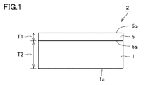
- FIG. 1 is a schematic cross-sectional view of a joined body according to an embodiment of the present disclosure.
- FIG. 2 is a perspective view showing an example of a bonded substrate having electrodes formed on the main surface of the bonded body of FIG.
- FIG. 3 is a sectional view of the bonded substrate of FIG. 2 taken along line XX.
- FIG. 4 is a schematic cross-sectional view of a surface acoustic wave device according to an embodiment of the present disclosure.
- FIG. 5 is a diagram for explaining the TTV.
- an object of the present invention is to provide a bonded body having a spinel polycrystal substrate, having a small variation and excellent frequency-temperature characteristics, and a surface acoustic wave device including the bonded body.
- a bonded body according to an aspect of the present disclosure includes a piezoelectric substrate and a spinel polycrystalline substrate provided on one main surface of the piezoelectric substrate, T1/T2, which is the ratio of the average thickness T1 of the piezoelectric substrate and the average thickness T2 of the spinel polycrystalline substrate, is 0.1 or less,
- the spinel polycrystalline substrate is a bonded body having TTV of 1.5 ⁇ m or less on the main surface in contact with the piezoelectric substrate.
- the bonded body includes the spinel polycrystalline substrate and can have excellent frequency-temperature characteristics with little variation.
- the frequency temperature characteristic (TCF) is a value (unit: ppm/° C.) indicating a change in frequency due to a change in ambient temperature. The smaller the value of TCF, the better the temperature characteristics.
- TTV is a value indicating the difference between the maximum value and the minimum value of the distance from the back surface of the substrate to the surface facing the back surface.
- the spinel polycrystalline substrate 51 shown in FIG. 5 the difference between the maximum value L1 and the minimum value L2 of the distance from the back surface 1a of the spinel polycrystalline substrate 51 to the surface (opposing surface) 1b facing the back surface 1a.
- the value L3 corresponds to TTV.
- T1/T2 is 0.0002 or more and 0.1 or less. According to this, it is possible to further reduce variations in frequency-temperature characteristics.
- the T1 is 0.1 ⁇ m or more and 25 ⁇ m or less
- the T2 is preferably 100 ⁇ m or more and 500 ⁇ m or less.
- the piezoelectric substrate can well suppress the loss of surface acoustic waves, and the spinel polycrystalline substrate can sufficiently suppress the thermal expansion of the piezoelectric substrate.
- the piezoelectric substrate is preferably made of lithium tantalate or lithium niobate. According to this, the electromechanical coupling coefficient of the piezoelectric substrate can be increased, and the frequency filter characteristic of the piezoelectric substrate can be improved.
- the total thickness of the T1 and the T2 is 100.1 ⁇ m or more and 525 ⁇ m or less
- the main surface of the spinel polycrystalline substrate is a circle having a diameter of 100 mm or more and 200 mm or less, or a shape in which an orientation flat is formed in the circle.
- the TTV of the outer surface of the joined body is preferably 10 ⁇ m or less.
- the piezoelectric substrate can satisfactorily suppress surface acoustic wave loss, and the bonded body can have excellent frequency-temperature characteristics with less variation.
- a surface acoustic wave device includes the above-mentioned bonded body, A surface acoustic wave device, comprising: an electrode provided on a main surface of the piezoelectric substrate opposite to a surface provided with the spinel polycrystalline substrate.
- the surface acoustic wave device can have excellent frequency-temperature characteristics with little variation.
- the notation in the form of “AB” means the upper and lower limits of the range (that is, A or more and B or less), and when A has no unit, B only has a unit.
- the unit of B and the unit of B are the same.
- the upper limit of the range being C means that the upper limit of the range is C or lower
- the lower limit of the range being D means that the lower limit of the range is D or higher.
- the bonded body 2 according to this embodiment is on a piezoelectric substrate 5 and one main surface (hereinafter, also referred to as “first main surface”) 5a of the piezoelectric substrate 5.
- first main surface a main surface
- spinel polycrystalline substrate 1 provided in the. T1/T2, which is the ratio of the average thickness T1 of the piezoelectric substrate and the average thickness T2 of the spinel polycrystalline substrate, is 0.1 or less, and the spinel polycrystalline substrate has a main surface in contact with the piezoelectric substrate.
- TTV is 1.5 ⁇ m or less.
- the present inventors have made a bonded body including a piezoelectric substrate and a spinel polycrystalline substrate provided on one main surface of the piezoelectric substrate, and have an average thickness of the piezoelectric substrate.
- T1/T2 which is the ratio of T1 to the average thickness T2 of the spinel polycrystalline substrate, is 0.1 or less, and the spinel polycrystalline substrate has a TTV of 1.5 ⁇ m or less on the main surface in contact with the piezoelectric substrate. It was newly found that the bonded body having the above-mentioned structure can have excellent frequency-temperature characteristics with little variation. The reason for this is not clear, but it is presumed to be as follows (i) and (ii).
- T1/T2 is 0.1 or less, and the average thickness T2 of the spinel polycrystalline substrate is sufficiently larger than the average thickness T1 of the piezoelectric substrate. Therefore, the spinel polycrystalline substrate can sufficiently suppress the thermal expansion of the piezoelectric substrate, and the bonded body can have excellent frequency-temperature characteristics with little variation.
- the spinel polycrystalline substrate has TTV of 1.5 ⁇ m or less on the main surface in contact with the piezoelectric substrate. Therefore, the spinel polycrystalline substrate has a uniform thickness, and the thermal expansion of the piezoelectric substrate can be sufficiently suppressed over the entire surface of the spinel polycrystalline substrate. Therefore, the bonded body can have excellent frequency-temperature characteristics with little variation.
- the average thickness of the bonded body 2 is preferably 100.1 ⁇ m or more and 525 ⁇ m or less, more preferably 200.1 ⁇ m or more and 510 ⁇ m or less, and further preferably 101 ⁇ m or more and 510 ⁇ m or less.
- the thickness of the bonded body is a value measured by a digital micrometer on a cross section parallel to the normal direction of the main surface of the bonded body. The measurement is performed at three points on one cross section, and the average value of the three points is taken as the average thickness of the bonded body.
- the main surface of the bonded body includes the front surface 5b of the piezoelectric substrate and the back surface 1a of the spinel polycrystalline substrate.
- the main surface of the bonded body is the front surface 5b of the piezoelectric substrate. Shall be indicated.
- the shape and size of the main surface of the bonded body 2 are not particularly limited, and can be appropriately adjusted depending on the application of the surface acoustic wave device.
- the main surface of the bonded body 2 includes both the main surface on the piezoelectric substrate 5 side and the main surface on the spinel polycrystalline substrate 1 side.
- the main surface of the bonded body 2 may be circular or rectangular, for example.
- the diameter thereof can be set to 100 mm or more and 200 mm or less.
- the main surface of the bonded body 2 has a rectangular shape, the length of one side thereof can be 70 mm or more and 142 mm or less.
- An orientation flat may be formed on the main surface of the bonded body 2.
- the TTV of the outer surface of the joined body 2 is preferably 10 ⁇ m or less.
- the method of joining the piezoelectric substrate 5 and the spinel polycrystalline substrate 1 is not particularly limited, and an adhesive may be used, or the van der Waals force may be used for joining.
- an adhesive may be used, or the van der Waals force may be used for joining.
- the piezoelectric substrate and the spinel polycrystalline substrate be bonded by Van der Waals force. More specifically, it is preferable that the atoms of the material forming the piezoelectric substrate and the atoms of the spinel forming the spinel polycrystalline substrate are joined by Van der Waals force.
- the piezoelectric substrate 5 is a substrate having a piezoelectric effect of converting an electric signal into mechanical vibration.
- the main component of the piezoelectric substrate 5 for example, lithium tantalate, lithium niobate, lithium borate or the like can be used. Among these, lithium tantalate or lithium niobate, which has an excellent electromechanical coupling coefficient, is preferable.
- the piezoelectric substrate 5 can be obtained, for example, by producing a single crystal ingot of the above-mentioned component by the Czochralski method and slicing this.
- the substrate orientation (cut angle) can be, for example, 36° to 50°, and can be appropriately selected according to the application of the surface acoustic wave device.
- the average thickness T1 of the piezoelectric substrate 5 is preferably 0.1 ⁇ m or more and 25 ⁇ m or less. When the average thickness T1 of the piezoelectric substrate 5 is less than 0.1 ⁇ m, the loss of surface acoustic waves may be large, or the processing of the piezoelectric substrate 5 may be difficult. When the average thickness T1 of the piezoelectric substrate 5 exceeds 25 ⁇ m, expansion or contraction of the piezoelectric substrate 5 due to temperature change may increase, or the bonded body 2 may become unnecessarily thick.
- the lower limit of the average thickness T1 of the piezoelectric substrate 5 is preferably 0.1 ⁇ m, more preferably 1 ⁇ m, even more preferably 3 ⁇ m.
- the upper limit of the average thickness T1 of the piezoelectric substrate 5 is preferably 25 ⁇ m, more preferably 15 ⁇ m, and even more preferably 10 ⁇ m.
- the average thickness of the piezoelectric substrate 5 is preferably 1 ⁇ m or more and 15 ⁇ m or less, more preferably 3 ⁇ m or more and 10 ⁇ m or less.
- the thickness of the piezoelectric substrate can be confirmed by measuring the thickness of the bonded body and the thickness of the spinel polycrystalline substrate and subtracting the thickness of the spinel polycrystalline substrate from the thickness of the bonded body.
- the thickness of the bonded body can be measured with a digital micrometer.
- the thickness of the spinel polycrystalline substrate can be measured with a micrometer.
- the upper limit of the arithmetic average roughness (Ra) of the first main surface 5a of the piezoelectric substrate 5 is preferably 1 nm, more preferably 0.8 nm. If the arithmetic average roughness (Ra) of the first main surface 5a of the piezoelectric substrate 5 exceeds 1 nm, the adhesive strength with the spinel polycrystalline substrate 1 due to Van der Waals force may be reduced. On the other hand, the lower limit of the arithmetic average roughness (Ra) of the first main surface 5a of the piezoelectric substrate 5 is preferably 0.05 nm.
- the arithmetic average roughness (Ra) of the first main surface 5a of the piezoelectric substrate 5 is less than 0.05 nm, bulk waves are likely to be reflected between the piezoelectric substrate 5 and the spinel polycrystalline substrate 1, resulting in spurious. There is a possibility that the response may be increased, or the adhesive area between the piezoelectric substrate 5 and the spinel polycrystalline substrate 1 may be reduced, and the adhesive strength between the piezoelectric substrate 5 and the spinel polycrystalline substrate 1 due to van der Waals force may be reduced. ..
- the arithmetic mean roughness means the arithmetic mean roughness defined in JIS B 0601.
- the arithmetic mean roughness is a value measured by an atomic force microscope (AFM: Atomic Force Microscope).
- the upper limit of the linear expansion coefficient of the piezoelectric substrate 5 is preferably 30 ⁇ 10 ⁇ 6 /° C., more preferably 20 ⁇ 10 ⁇ 6 /° C. When the coefficient of linear expansion of the piezoelectric substrate 5 exceeds 30 ⁇ 10 ⁇ 6 /° C., the expansion or contraction of the piezoelectric substrate due to the temperature change may increase.
- the lower limit of the linear expansion coefficient of the piezoelectric substrate 5 is not particularly limited, but for example, 8 ⁇ 10 ⁇ 6 /° C. is preferable, and 10 ⁇ 10 ⁇ 6 is more preferable.
- the above-mentioned linear expansion coefficient is a value measured by the compression load method ("Thermo-mechanical analyzer TMA8310" manufactured by Rigaku Corporation).
- the piezoelectric substrate 5 may include a component other than the above main components, for example, a metal may be added.
- the mechanical strength and heat resistance of the piezoelectric substrate 5 can be improved by adding the metal element.
- the spinel polycrystalline substrate 1 is a substrate made of a spinel sintered body.
- the spinel polycrystalline substrate 1 is a supporting base material for increasing the strength of the bonded body 2 and suppressing thermal expansion of the piezoelectric substrate.
- Examples of spinel that constitutes the spinel polycrystalline substrate 1 include MgO.nAl 2 O 3 (1 ⁇ n ⁇ 3).
- the lower limit of the value of n is preferably 1, more preferably 1.03, further preferably 1.05. When the value of n is less than 1, MgO locally increases and the porosity tends to increase.
- the upper limit of the value of n is preferably 3, more preferably 2, and even more preferably 1.5. When the value of n is greater than 3, the number of locally Al 2 O 3, the Al 2 O 3 is unevenly distributed with pores tend to visually on turbidity increases.
- composition of the spinel polycrystalline substrate and the value of n in the composition formula MgO.nAl 2 O 3 can be measured by the X-ray diffraction matrix flushing method.
- the spinel polycrystalline substrate 1 may include a component other than spinel, and can include, for example, an alumina component.
- the upper limit of the content of components other than spinel in the spinel polycrystalline substrate is preferably 10% by mass, and more preferably 5% by mass.
- the lower limit of the content of components other than spinel in the spinel polycrystalline substrate is preferably 3% by mass, more preferably 1% by mass, and 0, that is, it is even more preferable that no components other than spinel are contained.
- the average thickness T2 of the spinel polycrystalline substrate 1 is preferably 100 ⁇ m or more and 500 ⁇ m or less. When the average thickness T2 of the spinel polycrystalline substrate 1 is less than 100 ⁇ m, the thermal expansion of the piezoelectric substrate may not be sufficiently suppressed. If the average thickness T2 of the spinel polycrystalline substrate 1 exceeds 500 ⁇ m, bulk waves may be easily reflected at the boundary between the piezoelectric substrate 5 and the spinel polycrystalline substrate 1, and the bonded body 2 may be unnecessarily thick. is there.
- the lower limit of the average thickness T2 of the spinel polycrystalline substrate 1 is preferably 100 ⁇ m, more preferably 150 ⁇ m, even more preferably 200 ⁇ m.
- the upper limit of the average thickness T2 of the spinel polycrystalline substrate 1 is preferably 500 ⁇ m, more preferably 400 ⁇ m, even more preferably 300 ⁇ m.
- the average thickness T2 of the spinel polycrystalline substrate 1 is more preferably 150 ⁇ m or more and 400 ⁇ m or less, further preferably 200 ⁇ m or more and 300 ⁇ m or less.
- the above-mentioned thickness of the spinel polycrystalline substrate is a value measured by a micrometer on a cross section parallel to the normal direction of the back surface 1a of the spinel polycrystalline substrate. The measurement is performed at three points on one cross section, and the average value of the three points is taken as the average thickness of the piezoelectric substrate.
- the ratio T1/T2 which is the ratio between the average thickness T1 of the piezoelectric substrate 5 and the average thickness T2 of the spinel polycrystalline substrate 1, is 0.1 or less, and the ratio of the average thickness T1 of the piezoelectric substrate to the spinel polycrystalline substrate is The average thickness T2 is sufficiently large. Therefore, the spinel polycrystalline substrate can sufficiently suppress the thermal expansion of the piezoelectric substrate, and the bonded body can have excellent frequency-temperature characteristics with little variation.
- the upper limit of the ratio T1/T2 is 0.1, preferably 0.04, more preferably 0.02.
- T1/T2 exceeds 0.1, the frequency temperature characteristic (TCF) tends to deteriorate.
- the lower limit of the ratio T1/T2 is preferably 0.0002, more preferably 0.002, and even more preferably 0.006. If the ratio T1/T2 is less than 0.0002, the processing accuracy of the piezoelectric substrate 5 may decrease. Further, there is a risk that the deformation of the bonded body 4 due to a temperature change will increase or that the mechanical strength will decrease.
- the above ratio T1/T2 is preferably 0.0002 or more and 0.1 or less, more preferably 0.002 or more and 0.04, and further preferably 0.006 or more and 0.02 or less.
- the spinel polycrystalline substrate 1 has a TTV of 1.5 ⁇ m or less on the main surface in contact with the piezoelectric substrate 5 (corresponding to the facing surface 1b). Therefore, the film thickness of the spinel polycrystalline substrate is kept uniform, and thermal expansion of the piezoelectric substrate can be sufficiently suppressed over the entire surface of the spinel polycrystalline substrate. Therefore, the bonded body can have excellent frequency-temperature characteristics with little variation.
- the upper limit of TTV is 1.5 ⁇ m, preferably 1.2 ⁇ m, more preferably 0.9 ⁇ m, and further preferably 0.7 ⁇ m.
- TTV exceeds 1.5 ⁇ m, the film thickness of the spinel polycrystalline substrate becomes non-uniform, and the frequency-temperature characteristic of the bonded body tends to vary.
- the lower limit of TTV is not particularly limited, but 0.1 ⁇ m is preferable and 0.5 ⁇ m is more preferable from the viewpoint of manufacturing.
- TTV is preferably 0.1 ⁇ m or more and 1.5 ⁇ m or less, more preferably 0.1 ⁇ m or more and 1.2 ⁇ m or less, still more preferably 0.5 ⁇ m or more and 0.7 ⁇ m or less.
- the above TTV is measured by a flatness measuring device (“FlatMaster 200XRA-Wafer” manufactured by Tropel).
- the measurement area is the entire area of the main surface (corresponding to the facing surface 1b) of the spinel polycrystalline substrate in the bonded body which is in contact with the piezoelectric substrate.
- the total thickness of T1 and T2 is 100.1 ⁇ m or more and 525 ⁇ m or less
- the spinel polycrystalline substrate has a main surface of a circle having a diameter of 100 mm or more and 200 mm or less, or a shape in which an orientation flat is formed in the circle.
- the TTV of the main surface of the spinel polycrystalline substrate in contact with the piezoelectric substrate is 1.5 ⁇ m or less
- the TTV on the outer surface of the bonded body can be 10 ⁇ m or less.
- the spinel polycrystalline substrate includes a plurality of crystal grains, and the crystal grains preferably have an average grain size of 1 ⁇ m or more and 60 ⁇ m or less. According to this, the loss of elastic waves can be suppressed more effectively.
- the average grain size of the crystal grains is less than 1 ⁇ m, the porosity of the spinel polycrystalline substrate becomes too large and the elastic modulus decreases, so it is difficult to obtain the effect as a supporting substrate of suppressing the thermal expansion of the piezoelectric substrate. Tend. Furthermore, since the contact area at the bonding interface between the spinel polycrystalline substrate and the piezoelectric substrate is reduced, the bonding strength is reduced. On the other hand, when the average grain size of the crystal grains exceeds 60 ⁇ m, pores existing at grain boundaries between spinel grains tend to be unevenly distributed.
- the average grain size of the spinel polycrystalline substrate is more preferably 5 ⁇ m or more and 30 ⁇ m or less, and further preferably 8 ⁇ m or more and 30 ⁇ m or less.
- the “average particle diameter” means a median diameter (d50) in a volume-based particle size distribution (volume distribution), and an average particle diameter for all spinel particles contained in a spinel polycrystalline substrate. Means that.
- the particle size of each particle for calculating the average particle size of spinel particles can be measured by the following method. First, the surface of the spinel polycrystalline substrate is mirror-polished, and a measurement field of 10 mm ⁇ 10 mm is determined on the polished surface. A backscattered electron image of the spinel polycrystalline substrate in the measurement visual field is observed with an electron microscope at a magnification of 5000 times. Next, in this backscattered electron image, the diameter of the circle circumscribing the particles forming the spinel polycrystalline substrate (that is, the diameter equivalent to the circumscribing circle) is measured, and the diameter is defined as the particle diameter of the spinel particles.
- the lower limit of the arithmetic mean roughness (Ra) of the surface of the spinel polycrystalline substrate 1 is preferably 0.01 nm, more preferably 0.1 nm.
- the arithmetic average roughness (Ra) of the surface of the spinel polycrystalline substrate 1 is less than 0.01 nm, it is necessary to process the surface of the spinel polycrystalline substrate 1 to be extremely flat, which increases the processing cost.
- the upper limit of the arithmetic average roughness (Ra) of the surface of the spinel polycrystalline substrate 1 is preferably 3.0 nm, more preferably 2.0 nm.
- the upper limit of the linear expansion coefficient of the spinel polycrystalline substrate 1 is preferably 16 ⁇ 10 ⁇ 6 /° C., more preferably 8 ⁇ 10 ⁇ 6 /° C. If the linear expansion coefficient of the spinel polycrystalline substrate 1 exceeds 16 ⁇ 10 ⁇ 6 /° C., the thermal expansion of the piezoelectric substrate may not be sufficiently suppressed.
- the lower limit of the linear expansion coefficient of the spinel polycrystalline substrate 1 is preferably 1 ⁇ 10 ⁇ 6 /° C., more preferably 3 ⁇ 10 ⁇ 6 /° C.
- the linear expansion coefficient of the spinel polycrystalline substrate 1 is less than 1 ⁇ 10 ⁇ 6 /° C., the difference between the linear expansion coefficient of the spinel polycrystalline substrate 1 and that of the piezoelectric substrate 5 becomes large, and the strain of the spinel polycrystalline substrate 1 may increase when the temperature changes. is there.
- the above-mentioned linear expansion coefficient is a value obtained by measuring a rod-shaped material with a linear thermal expansion measuring device.
- the lower limit of the difference in linear expansion coefficient between the spinel polycrystalline substrate 1 and the piezoelectric substrate 5 is preferably 5 ⁇ 10 ⁇ 6 /° C., more preferably 7 ⁇ 10 ⁇ 6 /° C. If the difference in linear expansion coefficient between the spinel polycrystalline substrate 1 and the piezoelectric substrate 5 is less than 5 ⁇ 10 ⁇ 6 /° C., the thermal expansion of the piezoelectric substrate may not be sufficiently suppressed.
- the upper limit of the difference in linear expansion coefficient between the spinel polycrystalline substrate 1 and the piezoelectric substrate 5 is preferably 20 ⁇ 10 ⁇ 6 /°C. When the difference in linear expansion coefficient between the spinel polycrystalline substrate 1 and the piezoelectric substrate 5 exceeds 20 ⁇ 10 ⁇ 6 /° C., the strain of the spinel polycrystalline substrate 1 may increase when the temperature changes.
- the spinel polycrystalline substrate 1 supports a piezoelectric substrate 5 that vibrates when receiving an electric signal. Therefore, considerable stress is applied to the spinel polycrystalline substrate 1.
- the piezoelectric substrate 5 When the piezoelectric substrate 5 is activated, the piezoelectric substrate 5 generates heat, and the heat is also propagated to the spinel polycrystalline substrate 1. At this time, thermal stress is generated in the spinel polycrystalline substrate 1. For this reason, the spinel polycrystalline substrate 1 preferably has a corresponding strength.
- the lower limit of the Young's modulus of the spinel polycrystalline substrate 1 is preferably 100 GPa, more preferably 150 GPa, even more preferably 180 GPa. If the Young's modulus of the spinel polycrystalline substrate 1 is less than 100 GPa, the spinel polycrystalline substrate 1 may be easily cracked.
- the upper limit of the Young's modulus of the spinel polycrystalline substrate 1 is preferably 400 GPa, more preferably 350 GPa, further preferably 300 GPa. If the Young's modulus of the spinel polycrystalline substrate 1 exceeds 400 GPa, the hardness of the spinel polycrystalline substrate 1 becomes excessively high, so that chipping is likely to occur. Further, since the hardness of the spinel polycrystalline substrate 1 becomes excessively high, it may be difficult to process it.
- the Young's modulus is a value measured by a three-point bending test performed according to JIS R 1602.
- a “Material Testing Machine AL-50NB” manufactured by Minebea Co., Ltd. is used for the measurement.
- the lower limit of the Knoop hardness of the spinel polycrystalline substrate 1 is preferably 1000, more preferably 1200. If the Knoop hardness of the spinel polycrystalline substrate 1 is less than 1000, the spinel polycrystalline substrate 1 may be easily cracked.
- the upper limit of the Knoop hardness of the spinel polycrystalline substrate 1 is preferably 2500 and more preferably 1800. If the Knoop hardness of the spinel polycrystalline substrate 1 exceeds 2500, it may be difficult to process the spinel polycrystalline substrate 1.
- Knoop hardness is a value measured by "Hardness Testing Machine HM” manufactured by Mitutoyo Corporation.
- the method for manufacturing a bonded body according to the present embodiment includes a step of preparing a piezoelectric substrate, a step of preparing a spinel polycrystalline substrate, and a step of bonding the piezoelectric substrate and the spinel polycrystalline substrate to obtain a bonded body ( Hereinafter, also referred to as “bonding step”) and a step of adjusting the thickness of the piezoelectric substrate.
- a piezoelectric substrate is prepared.
- a conventionally known piezoelectric substrate can be used as the piezoelectric substrate.
- the main surface of the piezoelectric substrate is polished. Specifically, after the main surface of the piezoelectric substrate is roughly polished by grinding, the arithmetic mean roughness (Ra) is measured by CMP (Chemical Mechanical Polishing) with respect to the surface to which the spinel polycrystalline substrate is bonded. Is reduced to about 0.05 ⁇ m or more and about 1 ⁇ m or less.
- the step of preparing the spinel polycrystalline substrate can include a spinel powder preparation step, a forming step, a sintering step, and a processing step.
- a powder having a composition formula of MgO.nAl 2 O 3 (1 ⁇ n ⁇ 3) and made of spinel is prepared.
- the spinel powder preferably has an average particle size of 0.1 ⁇ m or more and 0.3 ⁇ m or less and a purity of 99.5% or more.
- the mixing ratio (mass ratio) of MgO (magnesium oxide) powder and Al 2 O 3 (alumina) powder is 1 ⁇ Al 2 O 3 /MgO ⁇ 3. It is preferable to mix them.
- the particle size of each particle to calculate the average particle size of the spinel powder is measured using the particle size distribution measurement method by the laser diffraction/scattering method. Specifically, it is a method of measuring the diameter of the powder particles by analyzing the scattered intensity distribution of the scattered light of the laser light irradiated on the powder particles.
- a molding process is performed. Specifically, a molded body is obtained by molding by press molding or CIP (Cold Isostatic Pressing). More specifically, it is preferable that the MgO.nAl 2 O 3 powder prepared in the spinel powder preparation step be first preformed by press forming and then CIP to obtain a formed body. Note that either one of press molding and CIP may be performed, or both may be performed, for example, CIP is performed after press molding.
- a pressure of 1 MPa or more and 300 MPa or less, particularly 10 MPa or more and 100 MPa or less is preferably used.
- CIP for example, it is preferable to use a pressure of 160 MPa or more and 250 MPa or less, particularly 180 MPa or more and 230 MPa or less.
- the molded body is sintered in a vacuum under a temperature condition of 1500° C. or more and 1700° C. or less for 60 minutes or more and 600 minutes or less (first sintering step), and then HIP (Hot Isostatic Pressing: hot Sintering is performed for 60 minutes or more and 240 minutes or less under the temperature condition of 1600° C. or more and 1800° C. or less by the isotropic pressure pressing method (second sintering step).
- HIP Hot Isostatic Pressing: hot Sintering is performed for 60 minutes or more and 240 minutes or less under the temperature condition of 1600° C. or more and 1800° C. or less by the isotropic pressure pressing method (second sintering step). This makes it possible to obtain a spinel ingot made of a spinel sintered body.
- the above second sintering step is preferably performed while changing the pressure in multiple steps. More specifically, under a temperature condition of 1600° C. or more and 1800° C. or less, a second a sintering step of sintering at a pressure of 100 MPa or more and 200 MPa or less for 1 minute or more and 60 minutes or less, and a temperature condition of 1600° C. or more and 1800° C. or less It is preferable to include a second b sintering step of sintering under a pressure of 150 MPa or more and 300 MPa or less for 10 minutes or more and 300 minutes or less.
- the obtained spinel ingot is sliced with a diamond wire saw so as to have a desired thickness.
- the base of the spinel polycrystalline substrate having a desired thickness is completed.
- the desired thickness is preferably determined in consideration of the thickness of the spinel polycrystalline substrate to be finally formed and the amount of polishing of the main surface of the spinel polycrystalline substrate in the subsequent step.
- the thickness T2 of the spinel polycrystalline substrate to be finally formed can be, for example, 100 ⁇ m or more and 500 ⁇ m or less.
- the main surface of the spinel polycrystalline substrate is polished. Specifically, after the main surface of the spinel polycrystalline substrate is roughly polished by grinding, the load on the substrate surface is evenly applied to the surface (opposing surface 1b) to which the piezoelectric substrate is finally joined. By performing the lapping process and the rough polishing process while keeping the balance as described above, the variation in the thickness from the back surface 1a is reduced so that the TTV is 1.5 ⁇ m or less.
- the lapping is performed by using a single-sided or double-sided lapping machine as a lapping machine and diamond abrasive grains as a lapping agent.
- the rough polishing is specifically performed using a single-sided or double-sided polishing machine. In each case, the work thickness and jig size are taken into consideration, and the work is performed while balancing so that the load is even.
- the spinel polycrystalline substrate can be bonded to the main surface of the piezoelectric substrate by Van der Waals force.
- the piezoelectric substrate prepared above and the spinel polycrystalline substrate are bonded to obtain a bonded body.
- the polishing surface of the spinel polycrystalline substrate and the polishing surface of the piezoelectric substrate face each other and are placed in the vacuum chamber. While maintaining this state, the internal gas in the chamber is exhausted to a high vacuum state. After that, the polished surfaces of both substrates are irradiated with a high-speed atom beam of neutralized argon, and then both substrates are brought into close proximity to each other to obtain a joined body.
- the second main surface 5b of the piezoelectric substrate is subjected to grinding, lapping and polishing so that the thickness T1 of the piezoelectric substrate becomes a desired thickness.
- the desired thickness is a thickness at which the value of T1/T2 is 0.1 or less, and can be, for example, 0.1 ⁇ m or more and 25 ⁇ m or less. This makes it possible to obtain a bonded body having a T1/T2 value of 0.1 or less.
- the TTV of the main surface (opposing surface 1b) of the spinel polycrystalline substrate in contact with the piezoelectric substrate was measured, and it was confirmed that the TTV of the spinel polycrystalline substrate before bonding was maintained.
- the surface acoustic wave device 10 is a surface on which the bonded body 2 described in the first embodiment and the spinel polycrystalline substrate 1 of the piezoelectric substrate 5 are provided.
- the electrode 3 is provided on the main surface (second main surface 5b) opposite to the (first main surface 5a).
- the bonded body 2 includes a piezoelectric substrate 5 and a spinel polycrystalline substrate provided on one main surface (first main surface 5a) of the piezoelectric substrate 5.
- the configurations of the bonded body, the piezoelectric substrate, and the spinel polycrystalline substrate used in this embodiment are the same as the configurations described in the first embodiment, and therefore the description thereof will not be repeated.
- the electrode 3 can include a first pole 3a and a second pole 3b. For example, an AC voltage is applied between the first pole 3a and the second pole 3b. Then, an electric signal is input to the current generated by the alternating voltage applied between the first pole 3a and the second pole 3b. Then, the crystal grains (atoms) forming the piezoelectric substrate 5 provided with the electrodes 3 are subjected to stress to approach or leave each other due to the piezoelectric effect, so that the main surface of the piezoelectric substrate 5 vibrates in a wavy manner.
- the first pole 3a and the second pole 3b can each have a comb shape. According to this, for example, among the electric signals input to the electrode 3, only the electric signal having a wavelength corresponding to the distance between the comb-shaped component 3c and the comb-shaped component 3d of the first pole 3a is propagated to the outside. That is, an electric signal having a wavelength other than the above-mentioned wavelength is not propagated to the outside and is blocked inside the bonded body 2.
- the bonded body 2 outputs only an electric signal having a desired wavelength to the outside, thereby blocking an electric signal (that is, noise) other than the desired wavelength and eliminating noise in the output signal. it can.
- an electrode member 6 can be further provided on the second main surface 5b of the piezoelectric substrate.
- the piezoelectric substrate 5, the electrode 3 provided on the second main surface 5b of the piezoelectric substrate, and the first main surface 5a of the piezoelectric substrate are formed on the piezoelectric substrate 5.
- the joined spinel polycrystalline substrate 1 forms a joined substrate 4.
- the bonding substrate 4 can further include the first electrode member 6.
- the surface acoustic wave device may be formed of only the bonding substrate 4, or may include other components in addition to the bonding substrate 4 as described below.
- An example in which the surface acoustic wave device includes another structure in addition to the bonded substrate 4 will be described with reference to FIG.
- the surface acoustic wave device 410 can further include a sealing substrate 7 for sealing the electrode 3 in addition to the bonding substrate 4.
- the second electrode member 9 made of a metal thin film is formed on the main surface of the sealing substrate 7 facing the bonding substrate 4, and the external terminals 11 are formed on the other main surface.
- the second electrode member 9 and the external terminal 11 are electrically connected via a via wiring 8 penetrating the sealing substrate 7.
- the first electrode member 6 and the second electrode member 9 are arranged so as to be in contact with each other, the first electrode member 6 and the external terminal 11 are also connected to the second electrode member 9 And are electrically connected via the via wiring 8.
- the bonding substrate 4 and the sealing substrate 7 are bonded via the adhesive member 13.
- the adhesive member 13 is provided so as to surround the electrode 3, the first electrode member 6, and the second electrode member 9. Therefore, the electrode 3, the first electrode member, and the second electrode member are shielded from the outside and hermetically sealed.
- the bonding substrate 4 and the sealing substrate 7 may be directly bonded by pressure bonding without using an adhesive member.
- metal or resin can be used as the adhesive member 13.
- metal gold, platinum, silver, copper, aluminum, nickel, titanium, gold alloy, a metal whose surface is coated with gold, or the like can be used.
- resin an epoxy resin, an acrylic resin, a silicone resin, a polyimide resin, a polyamide resin, a polyamideimide resin, or the like can be used.
- the average thickness of the sealing substrate 7 is preferably 10 ⁇ m or more and 1000 ⁇ m or less.
- the thickness of the surface acoustic wave device 410 is preferably 110.1 ⁇ m or more and 1550 ⁇ m or less.
- the main surface of the surface acoustic wave device 10 is preferably a rectangle whose one side length is 0.1 mm or more and 10 mm or less.
- the method for manufacturing a surface acoustic wave device includes a step of preparing a bonding substrate, a step of preparing a sealing substrate, and a step of bonding the bonding substrate and the sealing substrate to obtain a surface acoustic wave device. Can be provided.
- a bonded substrate is prepared.
- the bonded substrate can be obtained by forming electrodes on the main surface of the bonded body described in the first embodiment. Specifically, first, the surface of the piezoelectric substrate 5 in the bonded body 2 is cleaned by RCA cleaning. Next, an aluminum-based material to be an electrode is deposited on the polished surface of the piezoelectric substrate 5 by electron beam evaporation to a thickness of 100 to several hundred ⁇ .
- the RIE (Reactive Ion Etching) device removes the aluminum-based material that is not masked by the resist, leaving the aluminum-based material only in the electrode portion.
- the resist is removed to complete the electrode.
- the piezoelectric substrate 5, the electrode 3 provided on the second main surface 5b of the piezoelectric substrate 5, and the spinel polycrystalline substrate 1 bonded to the first main surface 5a of the piezoelectric substrate 5 are formed. It is possible to obtain the bonded substrate 4 including and.
- the first electrode member 6 can also be formed on the second main surface 5b of the piezoelectric substrate 5 by the same method as the method for producing the electrode 3 described above.
- the bonded substrate obtained above corresponds to the surface acoustic wave device 10.
- the following steps are further performed.
- the sealing substrate 7 for example, a substrate made of spinel is prepared. Via wirings 8 penetrating the substrate are formed on the substrate. Next, a second electrode member 9 is formed on one main surface of the substrate so as to cover the via wiring 8. Further, an external terminal 11 is formed on the other main surface of the substrate so as to cover the via wiring 8. Thereby, the sealing substrate 7 can be obtained.
- the obtained bonded substrate 4 and the sealing substrate 7 are bonded.
- the adhesive member 13 made of metal or resin is arranged on the second main surface 5b of the piezoelectric substrate 5.
- the sealing substrate 7 is arranged so as to face the second main surface 5b of the piezoelectric substrate 5.
- the first electrode member 6 and the second electrode member 9 are arranged so as to be in contact with each other.
- the sealing substrate 7 is pressed against the piezoelectric substrate 5 at a constant heating temperature, the sealing substrate 7 and the piezoelectric substrate 5 are bonded with the adhesive member 13, and the electrode 3 is hermetically sealed.
- the surface acoustic wave device 410 can be obtained by cutting the bonding substrate 4 and the sealing substrate 7 into a desired size while keeping the electrodes 3 hermetically sealed. Further, the surface acoustic wave device 410 may be obtained by cutting the bonded substrate 4 into a desired size and bonding it to the sealing substrate 7.
- a piezoelectric substrate made of lithium tantalate having an average thickness of 250 ⁇ m (shown as “average thickness P-T1” in Table 1) was prepared as the piezoelectric substrate.
- the shape of the main surface of the piezoelectric substrate was circular, and its diameter was ⁇ 98 mm.
- the surface to which the spinel polycrystalline substrate is bonded has an arithmetic mean roughness (Ra) of 0 by CMP (Chemical Mechanical Polishing).
- the surface roughness was reduced to about 5 nm.
- the spinel powder had an average particle size of 17 ⁇ m and a purity of 99.9%.
- the powder made of the above spinel was press-molded at a pressure of 10 MPa to obtain a molded body.
- the above-mentioned molded body was sintered in vacuum at 1675° C. for 4 hours, and then sintered under the conditions of pressure 200 MPa and temperature 1780° C. for 120 minutes. Thereby, a spinel ingot made of a spinel sintered body was obtained.
- the spinel ingot obtained was sliced with a diamond wire saw so as to have a desired average thickness, and a spinel polycrystalline substrate was obtained.
- the desired average thickness means the thickness of the spinel polycrystalline substrate shown in the "Average thickness PT2" column of the spinel polycrystalline substrate before bonding in Table 1 and the main surface of the spinel polycrystalline substrate in the subsequent step. It was decided after considering the polishing margin.
- the main surface of the spinel polycrystalline substrate had a circular shape, and the diameter was 100 mm.
- the surface to which the piezoelectric substrate is finally joined is balanced so that a load is evenly applied to the substrate surface.
- the lapping process and the rough polishing process while taking them, the variation in the thickness from the back surface was reduced so that the TTV became the value shown in the “P-TTV” column of the spinel polycrystalline substrate before bonding in Table 1.
- the lapping was performed using a single-sided or double-sided lapping machine as a lapping machine and diamond abrasive grains as a lapping agent.
- the rough polishing process was performed using a single-sided or double-sided polishing machine.
- the work thickness and the jig size were taken into consideration, and the work was performed while balancing the load so as to be uniform. Further, the surface roughness was reduced by CMP until the arithmetic average roughness (Ra) became about 0.5 nm.
- the spinel polycrystalline substrate prepared above was placed in a vacuum chamber such that the polished surface of the piezoelectric substrate and the polished surface of the piezoelectric substrate faced each other. While maintaining this state, the internal gas in the chamber was evacuated to a high vacuum state. After that, the polished surfaces of both substrates were irradiated with a high-speed atom beam of neutralized argon, and both substrates were brought into close proximity to each other to obtain a joined body.
- the second main part of the piezoelectric substrate is adjusted so that the thickness T1 of the piezoelectric substrate becomes the thickness shown in the “Average thickness T1” column of the piezoelectric substrate in the bonded substrate of Table 1.
- the surface was subjected to grinding, lapping and polishing.
- the average thickness T2 of the spinel polycrystalline substrate was measured.
- the results are shown in the "Average thickness T2" column of the spinel body crystal substrate in the joined body in Table 1. From the results in Table 1, it was confirmed that the average thickness P-T2 of the spinel polycrystalline substrate before bonding was the same as the average thickness T2 of the spinel polycrystalline substrate in the bonded body. Since the method of calculating average thickness T1 and average thickness T2 is described in the first embodiment, the description thereof will not be repeated.
- T1/T2 The value of T1/T2 was calculated from the obtained values of T1 and T2. The results are shown in the "T1/T2" column of Table 1.
- TTV of the interface between the spinel polycrystalline substrate and the piezoelectric substrate (corresponding to the facing surface 1b of the spinel polycrystalline substrate) was measured.
- the results are shown in the "TTV” column of the spinel polycrystalline substrate in the bonded body in Table 1. From the results in Table 1, it was confirmed that the TTV of the spinel polycrystalline substrate before bonding (“P-TTV” in Table 1) and the TTV of the spinel polycrystalline substrate in the bonded body were the same. Since the TTV measuring method is described in the first embodiment, the description thereof will not be repeated.
- the surface acoustic wave device pattern was exposed with a stepper exposure machine and developed by the developer.
- the RIE (Reactive Ion Etching: Reactive Ion Etching) device was used to remove the aluminum-based material that was not masked by the resist, leaving the aluminum-based material only in the electrode portion.
- the resist was removed to complete the electrode.
- the first electrode member was also formed on the second main surface of the piezoelectric substrate by the same method as the above-described electrode manufacturing method.
- a substrate made of spinel was prepared. Via wiring was formed on the substrate so as to penetrate the substrate. Next, a second electrode member was formed on one main surface of the substrate so as to cover the via wiring. Further, an external terminal was formed on the other main surface of the substrate so as to cover the via wiring. This obtained the sealing substrate.
- the bonding substrate and the sealing substrate were cut into a size of 1 mm ⁇ 1 mm with the electrodes kept airtightly sealed, to obtain surface acoustic wave devices of Sample 1 to Sample 19.
- TCF frequency temperature coefficient
- a network analyzer is connected to the SAW resonator of the surface acoustic wave device for testing from one substrate to five points, and the ambient temperature is changed from -40°C to 85°C, and the temperature coefficient of the frequency of the surface acoustic wave device of each sample ( TCF: Temperature Coefficient of Frequency was measured, and the average value and variation (standard deviation) thereof were calculated. The results are shown in the columns of "Average value” and "Variation” in Table 1.
- Samples 1 to 3, 5 to 14 and 16 to 19 have a ratio T1/T2, which is a ratio of the average thickness T1 of the piezoelectric substrate and the average thickness T2 of the spinel polycrystalline substrate, of 0.1 or less.
- the substrate has a TTV of 1.5 ⁇ m or less on the main surface in contact with the piezoelectric substrate, and corresponds to the embodiment.
- Samples 1 to 3, 5 to 14 and 16 to 19 had good frequency-temperature characteristics and their variations were small.
- Sample 4 has T1/T2 of over 0.1, which corresponds to the comparative example.
- the frequency temperature characteristic of Sample 4 was lower than that of the above example.
- Sample 15 has a TTV of over 1.5 ⁇ m and corresponds to a comparative example. Sample 15 had a large variation in frequency-temperature characteristics as compared with the above examples.
- 1,51 spinel polycrystalline substrate 1a back surface, 1b opposing surface, 2 bonded body, 3 electrode, 3a first pole, 3b second pole, 4 bonded substrate, 5 piezoelectric substrate, 5a first main surface, 5b first 2 main surface, 6 first electrode member, 7 sealing substrate, 8 via wiring, 9 second electrode member, 10,410 surface acoustic wave device, 11 external terminal, 13 adhesive member.
Landscapes
- Physics & Mathematics (AREA)
- Acoustics & Sound (AREA)
- Chemical & Material Sciences (AREA)
- Engineering & Computer Science (AREA)
- Materials Engineering (AREA)
- Surface Acoustic Wave Elements And Circuit Networks Thereof (AREA)
- Crystals, And After-Treatments Of Crystals (AREA)
Abstract
Description
前記圧電体基板の平均厚みT1と、前記スピネル多結晶基板の平均厚みT2との比であるT1/T2が0.1以下であり、
前記スピネル多結晶基板は、前記圧電体基板と接する主面において、TTV(Total Thickness Variation、全体厚みばらつき)が1.5μm以下である。
前記圧電体基板の前記スピネル多結晶基板の設けられた面とは反対側の主面上に設けられた電極とを備える、表面弾性波デバイスである。
本発明者らが特許文献1のスピネルからなる基板を用いた表面弾性波デバイスを作製してその性能を評価したところ、基板の強度は十分であるものの、周波数温度特性(TCF)にばらつきが生じる場合があることが確認された。
上記態様によれば、スピネル多結晶基板を備え、ばらつきの小さい、優れた周波数温度特性を有する接合体、及び、該接合体を備える表面弾性波デバイスを提供することが可能である。
最初に本開示の実施態様を列記して説明する。
前記圧電体基板の平均厚みT1と、前記スピネル多結晶基板の平均厚みT2との比であるT1/T2が0.1以下であり、
前記スピネル多結晶基板は、前記圧電体基板と接する主面において、TTVが1.5μm以下である、接合体である。
前記T2は、100μm以上500μm以下であることが好ましい。
前記スピネル多結晶基板は、その主表面が、直径100mm以上200mm以下の円形、又は、前記円形にオリエンテーションフラットが形成された形状であり、
前記接合体は、その外表面のTTVが10μm以下であることが好ましい。
前記圧電体基板の前記スピネル多結晶基板の設けられた面とは反対側の主面上に設けられた電極とを備える、表面弾性波デバイスである。
本開示の一実施形態に係る接合体及び表面弾性波デバイスの具体例を、以下に図面を参照しつつ説明する。本開示の図面において、同一の参照符号は、同一部分または相当部分を表すものである。また、長さ、幅、厚み、深さ等の寸法関係は図面の明瞭化と簡略化のために適宜変更されており、必ずしも実際の寸法関係を表すものではない。
<接合体>
本実施形態に係る接合体について、図1を用いて説明する。図1に示されるように、本実施形態に係る接合体2は、圧電体基板5と、該圧電体基板5の一方の主面(以下、「第1の主面」とも記す。)5a上に設けられたスピネル多結晶基板1とを備える。該圧電体基板の平均厚みT1と、該スピネル多結晶基板の平均厚みT2との比であるT1/T2が0.1以下であり、該スピネル多結晶基板は、該圧電体基板と接する主面において、TTVが1.5μm以下である。
接合体2の平均厚みは、100.1μm以上525μm以下が好ましく、200.1μm以上510μm以下がより好ましく、101μm以上510μm以下が更に好ましい。ここで、接合体の厚みは、接合体の主面の法線方向に平行な断面をデジタルマイクロメータで測定される値である。測定は一の断面において3箇所で行い、3箇所の平均値を接合体の平均厚みとする。
圧電体基板5とスピネル多結晶基板1との接合の方法は特に限定されず、接着剤を用いてもよいし、ファンデルワールス力により接合されてもよい。圧電体基板とスピネル多結晶基板とを高精度に接合するためには、圧電体基板とスピネル多結晶基板とはファンデルワールス力により接合されることが好ましい。より具体的には、圧電体基板を構成する材料の原子と、スピネル多結晶基板を構成するスピネルの原子とは、ファンデルワールス力により接合されることが好ましい。
圧電体基板5は、電気信号を機械的振動へ変換する圧電効果を奏する基板である。圧電体基板5の主成分としては、例えばタンタル酸リチウム、ニオブ酸リチウム、ホウ酸リチウム等を用いることができる。これらの中でも、電気機械結合係数に優れるタンタル酸リチウム又はニオブ酸リチウムが好ましい。圧電体基板5は、例えばチョクラルスキー法で上記成分の単結晶棒を生成し、これをスライスすることで得ることができる。なお、基板方位(カット角度)としては、例えば36°~50°とすることができ、表面弾性波デバイスの用途等に応じて適宜選択することができる。
スピネル多結晶基板1は、スピネル焼結体からなる基板である。スピネル多結晶基板1は、接合体2の強度を高めると共に、圧電体基板の熱膨張を抑制するための支持基材である。スピネル多結晶基板1を構成するスピネルとしては、例えば、MgO・nAl2O3(1≦n≦3)が挙げられる。nの値の下限は、1が好ましく、1.03がより好ましく、1.05が更に好ましい。nの値が1未満であると、MgOが局所的に多くなり、気孔率が増加する傾向がある。nの値の上限は、3が好ましく、2がより好ましく、1.5が更に好ましい。nの値が3を超えると、局所的にAl2O3が多くなり、該Al2O3が気孔とともに偏在し、目視上白濁が増加する傾向がある。
本実施形態に係る接合体の製造方法は、圧電体基板を準備する工程と、スピネル多結晶基板を準備する工程と、圧電体基板とスピネル多結晶基板とを接合して接合体を得る工程(以下、「接合工程」とも記す。)と、圧電体基板の厚みを調整する工程を備えることができる。
まず、圧電体基板を準備する。圧電体基板は、従来公知の圧電体基板を用いることができる。次に、圧電体基板の主表面を研磨する。具体的には、圧電体基板の主表面を、研削加工で粗研磨を行った後、スピネル多結晶基板を接合する面に対し、CMP(Chemical Mechanical Polishing)にて、算術平均粗さ(Ra)が0.05μm以上1μm以下程度になるまで面粗度を低減する。
スピネル多結晶基板を準備する工程は、スピネル粉末準備工程と、成形工程と、焼結工程と、加工工程とを含むことができる。
次に、上記で準備された圧電体基板とスピネル多結晶基板とを接合して接合体を得る。具体的には、スピネル多結晶基板の研磨面と、圧電体基板の研磨面とが向かい合うようにして真空チャンバ内に配置する。この状態を保持したまま、チャンバ内の内部ガスを排気して高真空状態とする。その後、両基板の研磨面に中性化アルゴンの高速原子ビームを照射した後、両基板を近接させて接合し、接合体を得る。
上記で得られた接合体において、圧電体基板の厚みT1が所望の厚みとなるように、圧電体基板の第2の主面5bに対して、研削、ラップ加工及び研磨加工を行う。ここで所望の厚みは、T1/T2の値が0.1以下となる厚みであり、例えば、0.1μm以上25μm以下とすることができる。これにより、T1/T2の値が0.1以下である接合体を得ることができる。
<表面弾性波デバイスの構成>
本実施形態に係る表面弾性波デバイスについて、図2~図4を用いて説明する。
本実施形態に係る表面弾性波デバイスの製造方法は、接合基板を準備する工程と、封止基板を準備する工程と、接合基板と封止基板とを接合して表面弾性波デバイスを得る工程とを備えることができる。
まず、接合基板を準備する。接合基板は、実施の形態1に記載の接合体の主表面上に電極を形成して得ることができる。具体的には、まず、接合体2中の圧電体基板5をRCA洗浄にて表面を清浄化する。次に、圧電体基板5の研磨面に電極となるアルミ系材料を電子ビーム蒸着で100~数100Å厚みで堆積する。
封止基板7としては、例えばスピネルからなる基板を準備する。該基板に、基板を貫通するビア配線8を形成する。次に、該基板の一方の主面上に、ビア配線8を覆うように第2の電極部材9を形成する。また、該基板の他方の主面上に、ビア配線8を覆うように外部端子11を形成する。これにより封止基板7を得ることができる。
次に、得られた接合基板4と封止基板7とを接合する。まず、圧電体基板5の第2の主面5b上に、金属または樹脂からなる接着部材13を配置する。次に、圧電体基板5の第2の主面5bと対向するように、封止基板7を配置する。この時、第1の電極部材6と第2の電極部材9とが接するように配置する。次に、封止基板7を一定の加熱温度で圧電体基板5に押し当て、接着部材13で、封止基板7と圧電体基板5とを接合し、電極3を気密封止する。
本実施の形態を実施例により更に具体的に説明する。ただし、これらの実施例により本実施の形態が限定されるものではない。
(圧電体基板を準備する工程)
圧電体基板として、平均厚み250μm(表1において、「平均厚みP-T1」と示す)でタンタル酸リチウムからなる圧電体基板を準備した。圧電体基板の主面の形状は円形であり、その直径はΦ98mmであった。
組成式がMgO・nAl2O3(n=1.03)であり、スピネルからなる粉末を準備した。スピネル粉末は、平均粒径が17μmであり、純度が99.9%であった。
次に上記の成形体を真空中で1675℃で4時間焼結した後、圧力200MPa、温度1780℃の条件下で120分間焼結した。これにより、スピネル焼結体からなるスピネルインゴットを得た。
次に、上記で準備されたスピネル多結晶基板の研磨面と、圧電体基板の研磨面とが向かい合うようにして真空チャンバ内に配置した。この状態を保持したまま、チャンバ内の内部ガスを排気して高真空状態とした。その後、両基板の研磨面に中性化アルゴンの高速原子ビームを照射した後、両基板を近接させて接合し接合体を得た。
上記で得られた接合体において、圧電体基板の厚みT1が表1の接合基板中の圧電体基板の「平均厚みT1」欄に示される厚みとなるように、圧電体基板の第2の主面に対して、研削、ラップ加工及び研磨加工を行った。

(接合基板を準備する工程)
上記の接合体中の圧電体基板をRCA洗浄にて表面を清浄化した。次に、圧電体基板の洗浄化面に電極となるアルミ系材料を電子ビーム蒸着で数100Å厚みで堆積した。
封止基板としては、スピネルからなる基板を準備した。該基板に、基板を貫通するビア配線を形成した。次に、該基板の一方の主面上に、ビア配線を覆うように第2の電極部材を形成した。また、該基板の他方の主面上に、ビア配線を覆うように外部端子を形成した。これにより封止基板を得た。
次に、得られた接合基板と封止基板とを接合した。まず、圧電体基板の第2の主面上に、樹脂からなる接着部材を配置した。次に、圧電体基板の第2の主面と対向するように、封止基板を配置した。この時、第1の電極部材と第2の電極部材とが接するように配置した。次に、封止基板を一定の加熱温度で圧電体基板に押し当て、接着部材で、封止基板と圧電体基板とを接合し、電極を気密封止した。
得られた表面弾性波デバイスについて、周波数温度係数を測定した。周波数温度係数の具体的な測定方法は下記の通りである。
試料1~3、5~14及び16~19は、圧電体基板の平均厚みT1と、スピネル多結晶基板の平均厚みT2との比であるT1/T2が0.1以下であり、スピネル多結晶基板は、圧電体基板と接する主面において、TTVが1.5μm以下であり、実施例に該当する。試料1~3、5~14及び16~19は、周波数温度特性が良好であり、そのばらつきも小さかった。
Claims (6)
- 圧電体基板と、前記圧電体基板の一方の主面上に設けられたスピネル多結晶基板とを備え、
前記圧電体基板の平均厚みT1と、前記スピネル多結晶基板の平均厚みT2との比であるT1/T2が0.1以下であり、
前記スピネル多結晶基板は、前記圧電体基板と接する主面において、TTVが1.5μm以下である、接合体。 - 前記T1/T2が0.0002以上0.1以下である、請求項1に記載の接合体。
- 前記T1は、0.1μm以上25μm以下であり、
前記T2は、100μm以上500μm以下である、請求項1又は請求項2に記載の接合体。 - 前記圧電体基板は、タンタル酸リチウム又はニオブ酸リチウムからなる、請求項1から請求項3のいずれか1項に記載の接合体。
- 前記T1及び前記T2の合計厚みは、100.1μm以上525μm以下であり、
前記スピネル多結晶基板は、その主表面が、直径100mm以上200mm以下の円形、又は、前記円形にオリエンテーションフラットが形成された形状であり、
前記接合体は、その外表面のTTVが10μm以下である、請求項1から請求項4のいずれか1項に記載の接合体。 - 請求項1から請求項5のいずれか1項に記載の接合体と、
前記圧電体基板の前記スピネル多結晶基板の設けられた面とは反対側の主面上に設けられた電極とを備える、表面弾性波デバイス。
Priority Applications (7)
| Application Number | Priority Date | Filing Date | Title |
|---|---|---|---|
| CN201980089344.5A CN113316896A (zh) | 2019-01-18 | 2019-01-18 | 接合体及表面弹性波器件 |
| US17/422,774 US12308817B2 (en) | 2019-01-18 | 2019-01-18 | Joined body and surface acoustic wave device |
| JP2020566089A JP7339283B2 (ja) | 2019-01-18 | 2019-01-18 | 接合体及び表面弾性波デバイス |
| PCT/JP2019/001551 WO2020148908A1 (ja) | 2019-01-18 | 2019-01-18 | 接合体及び表面弾性波デバイス |
| CN202511048669.2A CN120934485A (zh) | 2019-01-18 | 2019-01-18 | 接合体及表面弹性波器件 |
| JP2023001169A JP7658993B2 (ja) | 2019-01-18 | 2023-01-06 | 接合体及び表面弾性波デバイス |
| JP2024193625A JP2025016704A (ja) | 2019-01-18 | 2024-11-05 | 接合体及び表面弾性波デバイス |
Applications Claiming Priority (1)
| Application Number | Priority Date | Filing Date | Title |
|---|---|---|---|
| PCT/JP2019/001551 WO2020148908A1 (ja) | 2019-01-18 | 2019-01-18 | 接合体及び表面弾性波デバイス |
Publications (1)
| Publication Number | Publication Date |
|---|---|
| WO2020148908A1 true WO2020148908A1 (ja) | 2020-07-23 |
Family
ID=71614491
Family Applications (1)
| Application Number | Title | Priority Date | Filing Date |
|---|---|---|---|
| PCT/JP2019/001551 Ceased WO2020148908A1 (ja) | 2019-01-18 | 2019-01-18 | 接合体及び表面弾性波デバイス |
Country Status (4)
| Country | Link |
|---|---|
| US (1) | US12308817B2 (ja) |
| JP (3) | JP7339283B2 (ja) |
| CN (2) | CN113316896A (ja) |
| WO (1) | WO2020148908A1 (ja) |
Families Citing this family (3)
| Publication number | Priority date | Publication date | Assignee | Title |
|---|---|---|---|---|
| JP7805476B2 (ja) * | 2022-12-30 | 2026-01-23 | 泉州市三安集成電路有限公司 | 基板構造、フィルタ及びデュプレクサ |
| CN121585125A (zh) * | 2022-12-30 | 2026-02-27 | 泉州市三安集成电路有限公司 | 一种滤波器器件 |
| CN119421633B (zh) * | 2025-01-06 | 2025-04-18 | 同济大学 | 基于尖晶石陶瓷衬底的异质结构衬底及其制备方法和应用 |
Citations (4)
| Publication number | Priority date | Publication date | Assignee | Title |
|---|---|---|---|---|
| JPH07335513A (ja) * | 1994-06-09 | 1995-12-22 | Nippondenso Co Ltd | 半導体基板の製造方法 |
| JP2014229943A (ja) * | 2013-05-17 | 2014-12-08 | 住友電気工業株式会社 | 圧電基板及び弾性表面波素子 |
| WO2015053127A1 (ja) * | 2013-10-10 | 2015-04-16 | 住友電気工業株式会社 | Iii族窒化物複合基板およびその製造方法、積層iii族窒化物複合基板、ならびにiii族窒化物半導体デバイスおよびその製造方法 |
| JP2017034363A (ja) * | 2015-07-29 | 2017-02-09 | 太陽誘電株式会社 | 弾性波デバイスおよびモジュール |
Family Cites Families (13)
| Publication number | Priority date | Publication date | Assignee | Title |
|---|---|---|---|---|
| JP2006304206A (ja) | 2005-04-25 | 2006-11-02 | Shin Etsu Chem Co Ltd | 弾性表面波素子及び複合圧電チップ並びにその製造方法 |
| JP4768520B2 (ja) | 2006-05-31 | 2011-09-07 | 太陽誘電株式会社 | 弾性表面波デバイス |
| JP5549167B2 (ja) * | 2009-09-18 | 2014-07-16 | 住友電気工業株式会社 | Sawデバイス |
| WO2011034136A1 (ja) | 2009-09-18 | 2011-03-24 | 住友電気工業株式会社 | 基板、基板の製造方法、sawデバイスおよびデバイス |
| WO2012033125A1 (ja) | 2010-09-07 | 2012-03-15 | 住友電気工業株式会社 | 基板、基板の製造方法およびsawデバイス |
| JP2014147054A (ja) * | 2013-01-30 | 2014-08-14 | Sumitomo Electric Ind Ltd | 圧電基板及び弾性表面波素子 |
| WO2015012005A1 (ja) | 2013-07-25 | 2015-01-29 | 日本碍子株式会社 | 複合基板及びその製法 |
| JP6488667B2 (ja) | 2014-11-21 | 2019-03-27 | 住友電気工業株式会社 | 表面弾性波デバイス |
| FR3045933B1 (fr) * | 2015-12-22 | 2018-02-09 | Soitec | Substrat pour un dispositif a ondes acoustiques de surface ou a ondes acoustiques de volume compense en temperature |
| US10340886B2 (en) | 2016-03-22 | 2019-07-02 | Sumitomo Electric Industries, Ltd. | Ceramic substrate, layered body, and saw device |
| WO2018151146A1 (ja) | 2017-02-16 | 2018-08-23 | 株式会社弾性波デバイスラボ | 弾性波素子およびその製造方法 |
| JP7061005B2 (ja) * | 2018-04-20 | 2022-04-27 | 太陽誘電株式会社 | 弾性波共振器、フィルタおよびマルチプレクサ |
| US11595019B2 (en) * | 2018-04-20 | 2023-02-28 | Taiyo Yuden Co., Ltd. | Acoustic wave resonator, filter, and multiplexer |
-
2019
- 2019-01-18 WO PCT/JP2019/001551 patent/WO2020148908A1/ja not_active Ceased
- 2019-01-18 CN CN201980089344.5A patent/CN113316896A/zh active Pending
- 2019-01-18 US US17/422,774 patent/US12308817B2/en active Active
- 2019-01-18 CN CN202511048669.2A patent/CN120934485A/zh active Pending
- 2019-01-18 JP JP2020566089A patent/JP7339283B2/ja active Active
-
2023
- 2023-01-06 JP JP2023001169A patent/JP7658993B2/ja active Active
-
2024
- 2024-11-05 JP JP2024193625A patent/JP2025016704A/ja not_active Withdrawn
Patent Citations (4)
| Publication number | Priority date | Publication date | Assignee | Title |
|---|---|---|---|---|
| JPH07335513A (ja) * | 1994-06-09 | 1995-12-22 | Nippondenso Co Ltd | 半導体基板の製造方法 |
| JP2014229943A (ja) * | 2013-05-17 | 2014-12-08 | 住友電気工業株式会社 | 圧電基板及び弾性表面波素子 |
| WO2015053127A1 (ja) * | 2013-10-10 | 2015-04-16 | 住友電気工業株式会社 | Iii族窒化物複合基板およびその製造方法、積層iii族窒化物複合基板、ならびにiii族窒化物半導体デバイスおよびその製造方法 |
| JP2017034363A (ja) * | 2015-07-29 | 2017-02-09 | 太陽誘電株式会社 | 弾性波デバイスおよびモジュール |
Also Published As
| Publication number | Publication date |
|---|---|
| US20220077839A1 (en) | 2022-03-10 |
| JP2023052257A (ja) | 2023-04-11 |
| US12308817B2 (en) | 2025-05-20 |
| JPWO2020148908A1 (ja) | 2021-12-23 |
| JP2025016704A (ja) | 2025-02-04 |
| CN113316896A (zh) | 2021-08-27 |
| CN120934485A (zh) | 2025-11-11 |
| JP7339283B2 (ja) | 2023-09-05 |
| JP7658993B2 (ja) | 2025-04-08 |
Similar Documents
| Publication | Publication Date | Title |
|---|---|---|
| JP7658993B2 (ja) | 接合体及び表面弾性波デバイス | |
| JP5549167B2 (ja) | Sawデバイス | |
| JP6375471B1 (ja) | 接合体および弾性波素子 | |
| US8614535B2 (en) | Substrate, manufacturing method of substrate and saw device | |
| US20120231218A1 (en) | Substrate, manufacturing method of substrate, saw device and device | |
| JP2018061258A (ja) | 表面弾性波デバイス用複合基板及びその製造方法とこの複合基板を用いた表面弾性波デバイス | |
| JP6563616B2 (ja) | 接合体および弾性波素子 | |
| JP2021517384A (ja) | 表面弾性波デバイス用のハイブリッド構造及び関連する製造方法 | |
| JP7414012B2 (ja) | 接合体及び表面弾性波デバイス | |
| JP7714072B2 (ja) | 表面弾性波素子用の複合基板およびその製造方法 | |
| JPWO2017051747A1 (ja) | 接合基板及びその製造方法とこの接合基板を用いた弾性表面波デバイス | |
| JP6488667B2 (ja) | 表面弾性波デバイス | |
| WO2019188350A1 (ja) | 接合体および弾性波素子 | |
| JPWO2018203430A1 (ja) | 弾性波素子およびその製造方法 | |
| JPWO2019039475A1 (ja) | 接合体および弾性波素子 | |
| JP7243743B2 (ja) | スピネル多結晶基板、接合体及び表面弾性波デバイス | |
| JP2026025934A (ja) | 支持基板、複合基板、電子デバイスおよびモジュール |
Legal Events
| Date | Code | Title | Description |
|---|---|---|---|
| 121 | Ep: the epo has been informed by wipo that ep was designated in this application |
Ref document number: 19910679 Country of ref document: EP Kind code of ref document: A1 |
|
| ENP | Entry into the national phase |
Ref document number: 2020566089 Country of ref document: JP Kind code of ref document: A |
|
| NENP | Non-entry into the national phase |
Ref country code: DE |
|
| 122 | Ep: pct application non-entry in european phase |
Ref document number: 19910679 Country of ref document: EP Kind code of ref document: A1 |
|
| WWG | Wipo information: grant in national office |
Ref document number: 17422774 Country of ref document: US |