WO2020145257A1 - 光信号処理装置 - Google Patents
光信号処理装置 Download PDFInfo
- Publication number
- WO2020145257A1 WO2020145257A1 PCT/JP2020/000137 JP2020000137W WO2020145257A1 WO 2020145257 A1 WO2020145257 A1 WO 2020145257A1 JP 2020000137 W JP2020000137 W JP 2020000137W WO 2020145257 A1 WO2020145257 A1 WO 2020145257A1
- Authority
- WO
- WIPO (PCT)
- Prior art keywords
- optical
- optical waveguide
- processing device
- signal processing
- switch
- Prior art date
- Legal status (The legal status is an assumption and is not a legal conclusion. Google has not performed a legal analysis and makes no representation as to the accuracy of the status listed.)
- Ceased
Links
Images


Classifications
-
- G—PHYSICS
- G02—OPTICS
- G02F—OPTICAL DEVICES OR ARRANGEMENTS FOR THE CONTROL OF LIGHT BY MODIFICATION OF THE OPTICAL PROPERTIES OF THE MEDIA OF THE ELEMENTS INVOLVED THEREIN; NON-LINEAR OPTICS; FREQUENCY-CHANGING OF LIGHT; OPTICAL LOGIC ELEMENTS; OPTICAL ANALOGUE/DIGITAL CONVERTERS
- G02F1/00—Devices or arrangements for the control of the intensity, colour, phase, polarisation or direction of light arriving from an independent light source, e.g. switching, gating or modulating; Non-linear optics
- G02F1/29—Devices or arrangements for the control of the intensity, colour, phase, polarisation or direction of light arriving from an independent light source, e.g. switching, gating or modulating; Non-linear optics for the control of the position or the direction of light beams, i.e. deflection
- G02F1/31—Digital deflection, i.e. optical switching
- G02F1/313—Digital deflection, i.e. optical switching in an optical waveguide structure
- G02F1/3136—Digital deflection, i.e. optical switching in an optical waveguide structure of interferometric switch type
-
- G—PHYSICS
- G02—OPTICS
- G02B—OPTICAL ELEMENTS, SYSTEMS OR APPARATUS
- G02B6/00—Light guides; Structural details of arrangements comprising light guides and other optical elements, e.g. couplings
- G02B6/24—Coupling light guides
- G02B6/26—Optical coupling means
- G02B6/28—Optical coupling means having data bus means, i.e. plural waveguides interconnected and providing an inherently bidirectional system by mixing and splitting signals
- G02B6/293—Optical coupling means having data bus means, i.e. plural waveguides interconnected and providing an inherently bidirectional system by mixing and splitting signals with wavelength selective means
- G02B6/29331—Optical coupling means having data bus means, i.e. plural waveguides interconnected and providing an inherently bidirectional system by mixing and splitting signals with wavelength selective means operating by evanescent wave coupling
-
- G—PHYSICS
- G02—OPTICS
- G02B—OPTICAL ELEMENTS, SYSTEMS OR APPARATUS
- G02B6/00—Light guides; Structural details of arrangements comprising light guides and other optical elements, e.g. couplings
- G02B6/24—Coupling light guides
- G02B6/26—Optical coupling means
- G02B6/28—Optical coupling means having data bus means, i.e. plural waveguides interconnected and providing an inherently bidirectional system by mixing and splitting signals
- G02B6/293—Optical coupling means having data bus means, i.e. plural waveguides interconnected and providing an inherently bidirectional system by mixing and splitting signals with wavelength selective means
- G02B6/29346—Optical coupling means having data bus means, i.e. plural waveguides interconnected and providing an inherently bidirectional system by mixing and splitting signals with wavelength selective means operating by wave or beam interference
- G02B6/2935—Mach-Zehnder configuration, i.e. comprising separate splitting and combining means
- G02B6/29352—Mach-Zehnder configuration, i.e. comprising separate splitting and combining means in a light guide
- G02B6/29355—Cascade arrangement of interferometers
-
- G—PHYSICS
- G02—OPTICS
- G02F—OPTICAL DEVICES OR ARRANGEMENTS FOR THE CONTROL OF LIGHT BY MODIFICATION OF THE OPTICAL PROPERTIES OF THE MEDIA OF THE ELEMENTS INVOLVED THEREIN; NON-LINEAR OPTICS; FREQUENCY-CHANGING OF LIGHT; OPTICAL LOGIC ELEMENTS; OPTICAL ANALOGUE/DIGITAL CONVERTERS
- G02F1/00—Devices or arrangements for the control of the intensity, colour, phase, polarisation or direction of light arriving from an independent light source, e.g. switching, gating or modulating; Non-linear optics
- G02F1/29—Devices or arrangements for the control of the intensity, colour, phase, polarisation or direction of light arriving from an independent light source, e.g. switching, gating or modulating; Non-linear optics for the control of the position or the direction of light beams, i.e. deflection
- G02F1/31—Digital deflection, i.e. optical switching
- G02F1/313—Digital deflection, i.e. optical switching in an optical waveguide structure
-
- G—PHYSICS
- G02—OPTICS
- G02B—OPTICAL ELEMENTS, SYSTEMS OR APPARATUS
- G02B6/00—Light guides; Structural details of arrangements comprising light guides and other optical elements, e.g. couplings
- G02B6/10—Light guides; Structural details of arrangements comprising light guides and other optical elements, e.g. couplings of the optical waveguide type
- G02B6/12—Light guides; Structural details of arrangements comprising light guides and other optical elements, e.g. couplings of the optical waveguide type of the integrated circuit kind
- G02B6/122—Basic optical elements, e.g. light-guiding paths
- G02B6/125—Bends, branchings or intersections
Definitions
- the present invention relates to an optical signal processing device, and more particularly to an optical signal processing device having an optical switch function.
- CDC Color-less, Direction-less, Contention-less
- ROADM Reconfigurable Optical Add/Drop Multiplexer
- MCS MultiCast Switch: MCS
- a transponder accommodated in the node to be routed in any direction (Color-less) without depending on the wavelength of signal light (Direction-
- An optical input/output device that serves as a key device that enables optical signals of the same wavelength that are assigned to different routes to be connected without collision (contention-less) within an optical node.
- MZI switch (Non-Patent Document 3) is often used as a switch element in the above MCS and PILOSS switches.
- FIG. 1A is a diagram showing an MZI switch that is an element configured as an optical waveguide and functioning as a switch element.
- an optical signal input from either of the two leftmost optical waveguides is branched into two upper and lower optical waveguides (arms) in the left directional coupler.
- a phase shifter formed on at least one of the optical waveguides gives a phase change, and as a result of recombining and interfering at the directional coupler on the right side, one of the two optical waveguides at the right end is switched according to the phase change ( Output).
- FIG. 1B is a diagram showing an optical signal processing device (switch) configured by connecting a plurality of switch elements such as a plurality of MCS switches and PILOS switches in multiple stages.
- switch optical signal processing device
- a plurality of MCS switches or PILOSS switches are used as switch elements, and these switches are connected in a plurality of stages in the z-axis direction, whereby the extinction ratio of the switches can be increased.
- the number of MZI switches required to configure switches of the same scale doubles.
- FIG. 2 shows a plan view of the basic structure of a conventional optical signal processing device.
- the overall waveguide direction of light is represented by the z-axis
- the direction of the row of switch elements by MZI is represented by the y-axis
- the yz plane corresponds to the substrate plane of the PLC (planar optical circuit). ing.
- the optical signal processing device shown in FIG. 2 has MZI switches, which are four switch elements, on the input side at the left end and four MZI switches, which are switch elements on the output side at the right end, and further has the MZI on the input side and the output side.
- the MZI switch which is a switch element, is also arranged between the MZI switch and the MZI switch on the side, and the MZI switches are connected by an optical waveguide.
- MZI switches are connected in four stages in each column in the y-axis direction.
- the optical waveguide and the optical waveguide forming the MZI switch are separated from each other. You need to be close. It is known that when the optical waveguides are close to each other, propagation mode coupling occurs, and an optical signal transfers from one optical waveguide to the other optical waveguide. Therefore, when the switch element interval is narrowed, optical signal leakage (crosstalk) between the optical signals occurs, which deteriorates the signal characteristics of the optical signals.
- the present invention has been made in view of the above problems, and an object of the present invention is to provide an optical signal processing device that reduces crosstalk while narrowing the interval between switch elements to reduce the size. It is in.
- an aspect of the present invention is an optical signal processing device.
- the optical signal processing device according to one embodiment, a plurality of input optical waveguides, a plurality of output optical waveguides, a plurality of optical waveguide elements arranged between the plurality of input optical waveguides and a plurality of output optical waveguides, A connection optical waveguide is provided, and a propagation constant of a connection optical waveguide adjacent to the optical waveguide element is different from a propagation constant of an optical waveguide configuring the adjacent optical waveguide element.
- FIG. 1 shows a switch element (MZI switch) constituted by an optical waveguide
- (b) is a diagram showing an optical signal processing device (switch) constituted by connecting a plurality of switch elements. It is a figure which shows the optical signal processing apparatus (switch) comprised by arranging a plurality of switch elements in the y-axis and z-axis directions, and connecting the output and input of a switch element.
- (A) is a figure which shows the structure of the optical signal processing apparatus of 1st Example
- (b) is a part of Fig.3 (a), and is an optical waveguide and switch element which connect switch elements to each other.
- FIG. 6 is a diagram showing an enlarged view of a region in which an optical waveguide that is not connected is in proximity. It is a figure which shows the structure of the optical signal processing apparatus of the 2nd Example. It is a figure which shows the structure of the optical signal processing apparatus of the 3rd Example.
- the multi-input multi-output optical switch of the PILOSS configuration has a configuration in which the output of the switch element in the front stage and the input of the switch element in the rear stage are connected among the switch elements connected in multiple stages.
- the optical signal processing device By configuring the optical signal processing device so as to satisfy the above, it is possible to reduce the distance between the switch elements while ensuring low crosstalk characteristics.
- the switch element is usually composed of an element mainly composed of an optical waveguide such as MZI (Fig. 1(a)), and is henceforth referred to as an optical waveguide element.
- the left end of the optical signal processing device will be described as the input side and the right end as the output side.
- the right end may be the input side and the left end may be the output side.
- the optical signal processing device may have a multi-stage configuration, and the optical waveguide on the output side of the optical waveguide element of each stage may be connected to the optical waveguide on the input side of the optical waveguide element of the next stage.
- the optical waveguide element on the output side of the preceding stage may be the optical waveguide element on the input side of the subsequent stage.
- FIG. 3A is a plan view of the connection optical waveguide and the switch element of the optical signal processing device according to the first embodiment of the present invention.
- FIG. 3A shows an optical signal processing device having a total of eight optical waveguide elements, four on the input side at the left end and four on the output side at the right end, as in the conventional example of FIG. .
- Eight optical waveguide elements are arranged between the four optical waveguide elements on the input side and the four optical waveguide elements on the output side.
- a total of 16 optical waveguide elements are arranged in 4 rows and 4 columns in the yz plane.
- Two sets of four connecting optical waveguides are connected between the input-side and output-side optical waveguide elements. Further, in FIG.
- the optical waveguides that are not connected to the 16 illustrated switch elements are arranged between the switch elements from left to right (the switch elements arranged in the second row in the y-axis direction and the third row). Between the switch elements arranged in the eye). As described above, when the distance between the optical waveguide elements in the y-axis direction is narrow, the propagation modes of the optical waveguides are coupled to each other, and crosstalk occurs between the optical waveguides.
- FIG. 3B is a diagram showing an optical waveguide formed between the switch elements in the third row (third from the left) of the second row and the third row in the y-axis direction in FIG. 3A.
- FIG. 3B shows the switch element of the second row (second from the left) and the second row of the second row and the third row in the y-axis direction in FIG. 3A when the switch element is MZI.
- region where the optical waveguide which connects each switch element of eye (the same 4th) (or the optical waveguide which comprises switch element) and the optical waveguide which is not connected to the illustrated switch element adjoins is shown.
- the coupling strength of the propagation modes of the adjacent optical waveguides becomes stronger as the distance between the optical waveguides becomes closer, even if the distance between them is short. Therefore, if the optical waveguides are too close to each other, crosstalk of optical signals will occur. Further, this coupling strength becomes the largest when the propagation constants of both are the same, and the value becomes small when the propagation constants of both are different.
- the propagation constant of the optical waveguide changes depending on the refractive index difference between the core and the clad, the refractive index distribution, and the shape of the core.
- the refractive indices of the core and cladding are usually determined at the time of creation, but it is possible to control the propagation constant by the shape of the adjacent optical waveguides. Is.
- the thickness of the optical waveguide can be controlled by the exposure mask when forming the core, and can be easily changed.
- the thickness of the optical waveguides adjacent to each other by changing the thickness of the optical waveguides adjacent to each other, the propagation constants of the two are changed, coupling of the propagation modes between them and the resulting crosstalk. Can be suppressed.
- the thickness (width in the y-axis direction) of the center optical waveguide among the three adjacent optical waveguides is configured to be thicker than the thickness of the other two optical waveguides.
- Two optical waveguides other than the central optical waveguide shown in FIG. 3B are provided with the switch elements of the second row and the third row of the third row (third from the left) in the y-axis direction of FIG. 3A.
- the propagation constants of two optical waveguides other than the central optical waveguide of FIG. may be different.
- the ratio of the thickness (width in the y-axis direction) of the two optical waveguides is set to 1.03 times.
- the optical waveguide whose both ends are connected to the switch element may be replaced with an optical waveguide whose at least one end is connected to the switch element, and/or an optical waveguide whose both ends are not connected to the switch element.
- At least one end may be replaced with an optical waveguide which is not connected to the switch element.
- there may be a configuration in which there is no one of the optical waveguide whose both ends are connected to the switch element and the optical waveguide whose both ends are not connected to the switch element.
- the propagation constants of the optical waveguides, at least one end of which is connected to the switch element may be different from the propagation constants of the optical waveguides that form the switch elements arranged close to each other in the y-axis direction.
- the propagation constants of the optical waveguides, at least one end of which is connected to the switch element may be different from the propagation constants of the optical waveguides that form the switch elements arranged close to each other in the y-axis direction.
- the switch elements arranged in proximity to each other in the y-axis direction there is no optical waveguide whose both ends are connected to the switch element and there is no optical waveguide whose both ends are not connected to the switch element.
- the propagation constants of the optical waveguides constituting the above may be different.
- FIG. 4 is a diagram simply showing the configuration of the optical signal processing device according to the second embodiment of the present invention.
- the optical signal processing device according to the present embodiment is a 4-input/3-output PILOSS switch, which connects the input and output optical waveguides, the switch element that is a two-dimensionally arranged MZI switch in the yz plane, and the switch elements. And a connecting optical waveguide.
- a PILOSS switch having an asymmetric input and output, there is a connection optical waveguide that skips each stage of the switch elements arranged in multiple stages and connects to the switch element of the next stage.
- the size of the entire switch can be reduced by placing the switch elements as close as possible.
- the propagation mode is generated between the connection optical waveguide formed between the switch elements and the optical waveguide forming the switch element (forming the MZI switch). Coupling and optical signal crosstalk will occur.
- the thickness of the connection optical waveguide formed between the switch elements different from the thickness of the optical waveguides that form the switch element, the propagation constants of the two change and the propagation mode coupling is weakened. Crosstalk of optical signals can be suppressed. Therefore, the distance between the optical waveguides in the optical signal processing device can be reduced, and the chip can be downsized.
- optical waveguides formed between the MZI switches to skip the MZI switches in each stage, but also in the adjacent MZI switches, by changing the propagation constants of the optical waveguides constituting the MZI switch, It is also possible to suppress the crosstalk of the optical signal between them. This can be achieved by using optical waveguides with different widths in adjacent MZI switches.
- FIG. 5 is a diagram simply showing the configuration of the optical signal processing device according to the third embodiment of the present invention.
- the optical signal processing device of this embodiment is a multicast switch (MCS) that adopts a 4-input 3-output PILOSS configuration, and is a switch that is an input and output optical waveguide and an MZI switch that is two-dimensionally arranged in the yz plane. It includes an element, a connection optical waveguide for connecting between the switch elements, and an optical splitter.
- MCS multicast switch
- the connection optical waveguide that skips each stage of the switch elements arranged in multiple stages and is connected to the switch element of the next stage is provided. Exists.
- the thickness of the connection optical waveguide formed between the switch elements different from the thickness of the optical waveguides forming the switch element, the propagation constants of the two are changed, and the propagation mode coupling is changed. By weakening, it is possible to suppress the crosstalk of the optical signal. Further, not only the optical waveguides formed between the MZI switches in order to skip the MZI switches in each stage, but also in the adjacent MZI switches, by changing the propagation constants of the optical waveguides constituting the MZI switches, the MZI switches can be changed. It is also possible to suppress the crosstalk of the optical signal between them.
Landscapes
- Physics & Mathematics (AREA)
- Nonlinear Science (AREA)
- General Physics & Mathematics (AREA)
- Optics & Photonics (AREA)
- Optical Modulation, Optical Deflection, Nonlinear Optics, Optical Demodulation, Optical Logic Elements (AREA)
- Optical Integrated Circuits (AREA)
Abstract
スイッチエレメントの間の間隔を狭くして小型化しつつ、クロストークを低減した光信号処理装置を提供する。複数の入力光導波路と、複数の出力光導波路と、複数の入力光導波路と複数の出力光導波路との間に配列された複数の光導波路素子と、接続光導波路とを備えた光信号処理装置であって、光導波路素子と近接する接続光導波路の伝搬定数が、当該近接する前記光導波路素子を構成する光導波路の伝搬定数と異なる。光導波路素子と近接する接続光導波路は、一端または両端が光導波路素子と接続されている接続光導波路または両端が光導波路素子と接続されていない接続光導波路である。
Description
本発明は、光信号処理装置に関し、より詳細には、光スイッチ機能を有する光信号処理装置に関する。
従来、光通信ネットワークでは、CDC(Color-less, Direction-less, Contention-less)-ROADM(Reconfigurable Optical Add/Drop Multiplexer)と呼ばれる光伝送通信方式の導入が進んでいる。CDC-ROADMネットワークのノードにおいて、マルチキャストスイッチ(MultiCast Switch:MCS) は、ノードに収容されているトランスポンダを、信号光の波長に依存することなく(Color-less)、任意の方路に(Direction-less)別方路に割り当てられる同一波長の光信号を光ノード内で衝突せずに(Contention-less)接続することを可能とする、キーデバイスとなる光入出力装置である。
光伝送装置の効率化のためには、MCSを小型化することが求められる。これまでに、PLC(Planar Lightwave Circuit:平面光回路)を利用し、PILOSS(Path-Independent insertion-Loss)と呼ばれる構成を採用した小型MCSが報告されている。(下記非特許文献1、2参照)
上記のようなMCSやPILOSSスイッチでのスイッチエレメントとしてマッハツェンダ干渉計(MZI:Mach-Zehnder Interferometer)スイッチ(非特許文献3)が多く採用されている。
図1(a)は、光導波路で構成されたスイッチエレメントとして機能する素子であるMZIスイッチを示す図である。図1(a)に示すMZIスイッチにおいて、左端の2つの光導波路のいずれかより入力された光信号は、左側の方向性結合器において上下2つの光導波路(アーム)に分岐され、2つのアーム光導波路の少なくとも一方に形成された位相シフタにより位相変化が与えられ、右側の方向性結合器において再び合波され干渉した結果、位相変化に応じて右端の2つの光導波路のいずれかより切り替え(スイッチング)出力される。
図1(b)は、複数のMCSスイッチやPILOSSスイッチなどのスイッチエレメントを複数段接続して構成された光信号処理装置(スイッチ)を示す図である。図1(b)に示すように複数のMCSスイッチやPILOSSスイッチをスイッチエレメントとして用い、これらをz軸方向に複数段接続することで、スイッチの消光比を上げることができる。この場合、同じ規模のスイッチを構成するために必要なMZIスイッチの数は倍になる 。
T. Watanabe, et. al., "Silica-based PLC Transponder Aggregateors for Colorless, Directionless, and Contentionless ROADM", OFC/NFOEC2012, OTh3D.1, March 8, 2012, Los Angeles
Takashi Goh, Akira Himeno, Masayuki Okuno, Hiroshi Takahashi, and Kuninori Hattori, "High-Extinction Ratio and Low-Loss Silica-Based 8x8 Strictly Nonblocking Thermooptic Matrix Switch", J. Lightwave Technology. VOL-17, NO.7, p-p 1192-1199, JULY 1999
T. Shibata et al., "Silica-based waveguide-type 16 x 16 optical switch module incorporating driving circuits," in IEEE Photonics Technology Letters, vol. 15, no. 9, pp. 1300-1302, Sept. 2003.
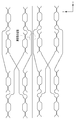
図2は、従来の光信号処理装置の基本構造の平面図を示す。本明細書において、光の全体的な導波方向をz軸として、MZIによるスイッチエレメントの列の方向をy軸として、y-z平面がPLC(平面光回路)の基板平面にあたるものとして表現している。
図2に示す光信号処理装置は、左端の入力側に4個のスイッチエレメントであるMZIスイッチおよび右端の出力側に4個のスイッチエレメントであるMZIスイッチを配置し、さらに入力側のMZIと出力側のMZIスイッチとの間にもスイッチエレメントであるMZIスイッチを配置し、MZIスイッチ間を光導波路で接続した構成である。y軸方向の各列においてMZIスイッチが4段に接続されている。図2には、各列の前段のMZIスイッチの出力と後段のMZIスイッチの入力を接続する光導波路の他に、y-z平面に配列されたMZIの内、y軸方向の2列目において3段に接続されたMZIスイッチの列と3列目において3段に接続されたMZIスイッチの列と間に形成された光導波路が含まれている。
しかしながら図2の従来の光信号処理装置の構成において、例えば光信号処理装置の小型化の理由により、スイッチエレメント間のy軸方向の間隔が小さくなると、MZIスイッチを構成する光導波路と光導波路が近接する必要が出てくる。光導波路同士が近接する場合、伝搬モードの結合が起こり、光信号が一方の光導波路から他方の光導波路に乗り移ることが知られている。そのため、スイッチエレメント間隔を狭めると光信号同士の光信号の漏れ(クロストーク)が発生し、光信号の信号特性を劣化させてしまう。
これを回避するためには、スイッチエレメントの間の間隔を十分に広くとる必要があり、結果的にPLCのチップサイズを大きくしてしまうという問題があった。
本発明は、このような問題に鑑みてなされたもので、その目的とするところは、スイッチエレメントの間の間隔を狭くして小型化しつつ、クロストークを低減した光信号処理装置を提供することにある。
このような目的を達成するために、本発明の態様は、光信号処理装置である。一実施形態にかかる光信号処理装置は、複数の入力光導波路と、複数の出力光導波路と、複数の入力光導波路と複数の出力光導波路との間に配列された複数の光導波路素子と、接続光導波路とを備え、光導波路素子と近接する接続光導波路の伝搬定数が、当該近接する前記光導波路素子を構成する光導波路の伝搬定数と異なることを特徴とする。
以上説明したように、本発明によれば、スイッチエレメントの間の間隔を狭くしつつ、クロストークを低減した光信号処理装置を実現することが可能となる。
本発明の基本的な考え方は、例えば以下の(i)-(iii)と言うことができる。
(i)PILOSS構成の多入力多出力の光スイッチは、多段接続されたスイッチエレメントの内の前段のスイッチエレメントの出力と後段のスイッチエレメントの入力とを接続した構成である。
(ii)特定の段のスイッチエレメントをスキップしたスイッチエレメント同士の接続等では、スイッチエレメント同士の間に光導波路を通す必要がある。(例えば、p列において多段に配列されたスイッチエレメントの内の、n段目のスイッチエレメントの出力とn+2番目のスイッチエレメントの入力とを接続する場合には、n+1番目のスイッチエレメントをスキップするための光導波路を、p列目のn+1番目のスイッチエレメントとp+1列目(またはp-1列目)のn+1番目のスイッチエレメントとの間に形成して接続する必要がある。)
(iii)上記(ii)のスイッチエレメントの間に形成された光導波路における伝搬定数を、スイッチエレメントを構成する光導波路の伝搬定数と異ならせることにより、スイッチエレメントを構成する光導波路とスイッチエレメントの間に形成された光導波路との間で生じる得る光信号のクロストーク(TX)を抑えることができる。
以上を満たすように光信号処理装置を構成することで、低クロストーク特性を確保しつつ、スイッチエレメントの間の間隔を狭くすることが可能となる。
なお、スイッチエレメントは通常、例えばMZIなどの光導波路を主体とした素子で構成されるため(図1(a))、以降の記載においては光導波路素子と称する。
以下、図面を参照しながら本発明の実施形態について詳細に説明する。なお、以下の各実施例の図において、光信号処理装置の左端を入力側、右端を出力側として説明するが、光導波路素子およびこれらを接続する光導波路における光の伝搬方向は可逆であって、右端を入力側、左端の出力側としてもよい。また、光信号処理装置は多段構成として、各段の光導波路素子の出力側の光導波路を次段の光導波路素子の入力側の光導波路に接続してもよい。あるいは、前段の出力側の光導波路素子が後段の入力側の光導波路素子となっていてもよい。
(実施例1)
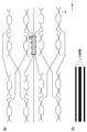
図3(a)は、本発明の実施例1に係る光信号処理装置の、接続光導波路とスイッチエレメントの平面図を示す。
図3(a)は、本発明の実施例1に係る光信号処理装置の、接続光導波路とスイッチエレメントの平面図を示す。
図3(a)において、簡単のため、図1の従来例と同じく左端の入力側に4個、右端の出力側に4個の計8個の光導波路素子を有する光信号処理装置が示される。入力側の4個の光導波路素子と出力側の4個の光導波路素子の間には、さらに8個の光導波路素子が配置されている。合計16個の光導波路素子は、y-z平面内に4行4列に配列されている。入力側と出力側の光導波路素子の間は、2組4本の接続光導波路で接続されている。また、図3(a)には、図示された16個のスイッチエレメントには接続されない光導波路が左から右へとスイッチエレメント間(y軸方向の2列目に配置されたスイッチエレメントと3列目に配列されたスイッチエレメントとの間)を通っている。前述したように、光導波路素子のy軸方向の間隔が狭いと光導波路同士の伝搬モードが結合し、光導波路間でクロストークが発生する。
図3(b)は、図3(a)におけるy軸方向の2列目及び3列目の3段目(左から3番目)のスイッチエレメント間に形成された光導波路を示す図である。図3(b)は、スイッチエレメントがMZIであった場合の、図3(a)におけるy軸方向の2列目及び3列目の2段目(左から2番目)のスイッチエレメントと4段目(同4番目)のスイッチエレメントをそれぞれ接続する光導波路(あるいはスイッチエレメントを構成する光導波路)と図示されたスイッチエレメントには接続されない光導波路とが近接する領域の拡大図を示す。
近接する光導波路の伝搬モードの結合強度は光導波路間隔が近くなると近接している距離が短くても強くなる。そのため、光導波路が近づき過ぎると、光信号のクロストークが発生してしまう。また、この結合強度は両者の伝搬定数が同一の時にもっとも大きくなり、両者の伝搬定数が異なる場合にはその値は小さくなる。
光導波路の伝搬定数はコアとクラッドの屈折率差や屈折率分布およびコアの形状により変化する。光信号処理装置が一つのチップ上に光導波路で形成されている場合、通常はコアとクラッドの屈折率は作成時に決まってしまうが、近接する光導波路の形状で伝搬定数を制御することは可能である。特に光導波路の太さはコアを形成する際の露光マスクで制御することができ、変更することが容易である。
本実施例では、図3(b)に示すように、近接する光導波路の太さを変えることにより、両者の伝搬定数を変化させ、両者間での伝搬モードの結合およびその結果もたらされるクロストークを抑えることができる。図3(b)においては、3本の隣接する光導波路の内の中心の光導波路の太さ(y軸方向の幅)を他の2本の光導波路の太さよりも太く構成している。図3(b)の中心の光導波路以外の2本の光導波路が、図3(a)のy軸方向の2列目及び3列目の3段目(左から3番目)のスイッチエレメントを構成する光導波路と隣接する場合には、これらを伝搬する光信号間のクロストークを低減するために、図3(b)の中心の光導波路以外の他の2本の光導波路の伝搬定数を、図3(a)のスイッチエレメントを構成する光導波路の伝搬定数と異ならせてもよい。
例えば、隣接する光導波路の間隔(y軸方向の距離)が40μmのとき、2つの光導波路の太さ(y軸方向の幅)の比が、1.03倍となるように2つの光導波路を構成することで、両者の伝搬係数を異ならせることにより、クロストークを抑えることができる。
上記例において、両端がスイッチエレメントに接続された光導波路は、少なくとも一端がスイッチエレメントには接続された光導波路に置き換えてもよく、および/または、両端がスイッチエレメントに接続されていない光導波路は、少なくとも一端がスイッチエレメントには接続されない光導波路に置き換えてもよい。または、上記例において、両端がスイッチエレメントに接続された光導波路および両端がスイッチエレメントに接続されていない光導波路のいずれか一方が無い構成としてもよい。この場合、少なくとも一端がスイッチエレメントに接続された光導波路の伝搬定数を、y軸方向において近接して配置されたスイッチエレメントを構成する光導波路の伝搬定数を異ならせてもよい。または少なくとも一端がスイッチエレメントに接続された光導波路の伝搬定数を、y軸方向において近接して配置されたスイッチエレメントを構成する光導波路の伝搬定数を異ならせてもよい。
また、上記例において、両端がスイッチエレメントに接続された光導波路および両端がスイッチエレメントに接続されていない光導波路が無い構成とし、y軸方向において近接して配置されたスイッチエレメントにおいて、当該スイッチエレメントを構成する光導波路の伝搬定数を異ならせてもよい。
(実施例2)
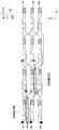
図4は、本発明の実施例2に係る光信号処理装置の構成を簡易的に示す図である。本実施例の光信号処理装置は4入力3出力のPILOSSスイッチであり、入力および出力光導波路と、y-z平面に2次元に配置されたMZIスイッチであるスイッチエレメントと、スイッチエレメント間を接続する接続光導波路とを含む。このような入力と出力が非対称なPILOSSスイッチでは、多段に並んだスイッチエレメントの各段をスキップし、次の段のスイッチエレメントに接続する接続光導波路が存在する。
図4は、本発明の実施例2に係る光信号処理装置の構成を簡易的に示す図である。本実施例の光信号処理装置は4入力3出力のPILOSSスイッチであり、入力および出力光導波路と、y-z平面に2次元に配置されたMZIスイッチであるスイッチエレメントと、スイッチエレメント間を接続する接続光導波路とを含む。このような入力と出力が非対称なPILOSSスイッチでは、多段に並んだスイッチエレメントの各段をスキップし、次の段のスイッチエレメントに接続する接続光導波路が存在する。
上述したように、スイッチエレメント間はできるだけ近づけることでスイッチ全体のサイズを縮小することができる。しかし、y軸方向のスイッチエレメントとスイッチエレメントとの間隔が小さすぎると、スイッチエレメント間に形成された接続光導波路とスイッチエレメントを構成する(MZIスイッチを構成する)光導波路との間で伝搬モード結合と光信号のクロストークが発生してしまう。
これに対し、スイッチエレメント間に形成された接続光導波路の太さを、スイッチエレメントを構成する光導波路の太さと異ならせることにより、両者の伝搬定数が変化し、伝搬モード結合を弱くすることで光信号のクロストークを抑えることができる。よって、光信号処理装置における光導波路間隔を小さくすることができ、チップを小型化することが可能となる。
また、各段のMZIスイッチをスキップするためにMZIスイッチ間に形成された光導波路のみならず、近接するMZIスイッチにおいて、当該MZIスイッチを構成する光導波路の伝搬定数を変化させることで、MZIスイッチ間での光信号のクロストークを抑制することもできる。これは、隣接するMZIスイッチにおいて、幅が異なる光導波路を採用することで達成することができる。
(実施例3)
図5は、本発明の実施例3の光信号処理装置の構成を簡易的に示す図である。本実施例の光信号処理装置は4入力3出力のPILOSS構成を採用したマルチキャストスイッチ(MCS)であり、入力および出力光導波路と、y-z平面に2次元に配置されたMZIスイッチであるスイッチエレメントと、スイッチエレメント間を接続する接続光導波路と、光スプリッタとを含む。このような入力と出力が非対称なPILOSS構成を採用したスイッチでは、実施例2と同様に、多段に並んだスイッチエレメントの各段をスキップし、次の段のスイッチエレメントに接続する接続光導波路が存在する。そのため、実施例2と同様に、スイッチエレメント間に形成された接続光導波路の太さを、スイッチエレメントを構成する光導波路の太さと異ならせることにより、両者の伝搬定数が変化し、伝搬モード結合を弱くすることで光信号のクロストークを抑えることができる。さらに、各段のMZIスイッチをスキップするためにMZIスイッチ間に形成された光導波路のみならず、近接するMZIスイッチにおいて、当該MZIスイッチを構成する光導波路の伝搬定数を変化させることで、MZIスイッチ間での光信号のクロストークを抑制することもできる。
図5は、本発明の実施例3の光信号処理装置の構成を簡易的に示す図である。本実施例の光信号処理装置は4入力3出力のPILOSS構成を採用したマルチキャストスイッチ(MCS)であり、入力および出力光導波路と、y-z平面に2次元に配置されたMZIスイッチであるスイッチエレメントと、スイッチエレメント間を接続する接続光導波路と、光スプリッタとを含む。このような入力と出力が非対称なPILOSS構成を採用したスイッチでは、実施例2と同様に、多段に並んだスイッチエレメントの各段をスキップし、次の段のスイッチエレメントに接続する接続光導波路が存在する。そのため、実施例2と同様に、スイッチエレメント間に形成された接続光導波路の太さを、スイッチエレメントを構成する光導波路の太さと異ならせることにより、両者の伝搬定数が変化し、伝搬モード結合を弱くすることで光信号のクロストークを抑えることができる。さらに、各段のMZIスイッチをスキップするためにMZIスイッチ間に形成された光導波路のみならず、近接するMZIスイッチにおいて、当該MZIスイッチを構成する光導波路の伝搬定数を変化させることで、MZIスイッチ間での光信号のクロストークを抑制することもできる。
Claims (8)
- 複数の入力光導波路と、複数の出力光導波路と、前記複数の入力光導波路と前記複数の出力光導波路との間に配列された複数の光導波路素子と、接続光導波路とを備えた光信号処理装置であって、
前記光導波路素子と近接する前記接続光導波路の伝搬定数が、当該近接する前記光導波路素子を構成する光導波路の伝搬定数と異なる、光信号処理装置。 - 前記接続光導波路は、少なくとも一端が前記光導波路素子と接続されている第1の接続光導波路を含み、前記第1の接続光導波路の伝搬定数が前記近接する前記光導波路素子を構成する光導波路の伝搬定数と異なる、請求項1に記載の光信号処理装置。
- 前記接続光導波路は、少なくとも一端が前記光導波路素子と接続されていない第2の接続光導波路を含み、
前記第2の接続光導波路の伝搬定数が前記近接する前記光導波路素子を構成する光導波路の伝搬定数と異なる、または、
前記第2の接続光導波路の伝搬定数が、少なくとも一端が前記光導波路素子と接続されている第1の接続光導波路の伝搬定数と異なる、請求項1または2に記載の光信号処理装置。 - 複数の入力光導波路と、複数の出力光導波路と、前記複数の入力光導波路と前記複数の出力光導波路との間に配列された複数の光導波路素子とを備えた光信号処理装置であって、
前記複数の光導波路素子の内の、光導波方向に直交する方向に近接して配列された2つの光導波路素子を構成する光導波路の伝搬定数が異なる、光信号処理装置。 - 伝搬定数が互いに異なる2つの光導波路は光導波路幅が異なる、請求項1乃至4のいずれか一項に記載の光信号処理装置。
- 前記光導波路素子がマッハツェンダ干渉計を含む、請求項1乃至5のいずれか一項に記載の光信号処理装置。
- 前記複数の光導波路素子は、光導波路素子を多段構成したPIOSS構成を光導波方向に直交する方向に配列した多入力多出力光スイッチを構成する、請求項1乃至6のいずれか一項に記載の光信号処理装置。
- 前記多入力多出力光スイッチは、マルチキャストスイッチの機能を有する、請求項7記載の光信号処理装置。
Priority Applications (1)
| Application Number | Priority Date | Filing Date | Title |
|---|---|---|---|
| US17/419,489 US12007665B2 (en) | 2019-01-10 | 2020-01-07 | Optical signal processing apparatus |
Applications Claiming Priority (2)
| Application Number | Priority Date | Filing Date | Title |
|---|---|---|---|
| JP2019-002856 | 2019-01-10 | ||
| JP2019002856A JP7189432B2 (ja) | 2019-01-10 | 2019-01-10 | 光信号処理装置 |
Publications (1)
| Publication Number | Publication Date |
|---|---|
| WO2020145257A1 true WO2020145257A1 (ja) | 2020-07-16 |
Family
ID=71521697
Family Applications (1)
| Application Number | Title | Priority Date | Filing Date |
|---|---|---|---|
| PCT/JP2020/000137 Ceased WO2020145257A1 (ja) | 2019-01-10 | 2020-01-07 | 光信号処理装置 |
Country Status (3)
| Country | Link |
|---|---|
| US (1) | US12007665B2 (ja) |
| JP (1) | JP7189432B2 (ja) |
| WO (1) | WO2020145257A1 (ja) |
Families Citing this family (1)
| Publication number | Priority date | Publication date | Assignee | Title |
|---|---|---|---|---|
| US12355494B2 (en) * | 2022-12-14 | 2025-07-08 | Hewlett Packard Enterprise Development Lp | Optical devices and systems for optical source redundancy |
Citations (7)
| Publication number | Priority date | Publication date | Assignee | Title |
|---|---|---|---|---|
| JPH09329720A (ja) * | 1996-06-10 | 1997-12-22 | Mitsubishi Gas Chem Co Inc | 集積型光導波路およびその製造法 |
| JP2005107229A (ja) * | 2003-09-30 | 2005-04-21 | Sumitomo Osaka Cement Co Ltd | 光導波路素子 |
| JP2007114222A (ja) * | 2005-03-31 | 2007-05-10 | Sumitomo Osaka Cement Co Ltd | 光制御素子 |
| JP2011128206A (ja) * | 2009-12-15 | 2011-06-30 | Nec Corp | アレイ導波路回折格子 |
| US20140294344A1 (en) * | 2013-03-28 | 2014-10-02 | Barthelemy Fondeur | Compact multicast switches, mxn switches and mxn splitters |
| JP2015075588A (ja) * | 2013-10-08 | 2015-04-20 | 古河電気工業株式会社 | 平面光導波路基板および光モジュール |
| JP2018036582A (ja) * | 2016-09-02 | 2018-03-08 | 日本電信電話株式会社 | モード合分波器及びモード多重伝送システム |
Family Cites Families (3)
| Publication number | Priority date | Publication date | Assignee | Title |
|---|---|---|---|---|
| JP5747004B2 (ja) * | 2012-08-22 | 2015-07-08 | 株式会社フジクラ | 光導波路素子 |
| WO2016070420A1 (zh) * | 2014-11-07 | 2016-05-12 | 华为技术有限公司 | 一种模式转换器、多模波导传输装置及方法 |
| CN111487713B (zh) * | 2016-02-18 | 2023-01-24 | 日本电信电话株式会社 | 光合波回路 |
-
2019
- 2019-01-10 JP JP2019002856A patent/JP7189432B2/ja active Active
-
2020
- 2020-01-07 US US17/419,489 patent/US12007665B2/en active Active
- 2020-01-07 WO PCT/JP2020/000137 patent/WO2020145257A1/ja not_active Ceased
Patent Citations (7)
| Publication number | Priority date | Publication date | Assignee | Title |
|---|---|---|---|---|
| JPH09329720A (ja) * | 1996-06-10 | 1997-12-22 | Mitsubishi Gas Chem Co Inc | 集積型光導波路およびその製造法 |
| JP2005107229A (ja) * | 2003-09-30 | 2005-04-21 | Sumitomo Osaka Cement Co Ltd | 光導波路素子 |
| JP2007114222A (ja) * | 2005-03-31 | 2007-05-10 | Sumitomo Osaka Cement Co Ltd | 光制御素子 |
| JP2011128206A (ja) * | 2009-12-15 | 2011-06-30 | Nec Corp | アレイ導波路回折格子 |
| US20140294344A1 (en) * | 2013-03-28 | 2014-10-02 | Barthelemy Fondeur | Compact multicast switches, mxn switches and mxn splitters |
| JP2015075588A (ja) * | 2013-10-08 | 2015-04-20 | 古河電気工業株式会社 | 平面光導波路基板および光モジュール |
| JP2018036582A (ja) * | 2016-09-02 | 2018-03-08 | 日本電信電話株式会社 | モード合分波器及びモード多重伝送システム |
Also Published As
| Publication number | Publication date |
|---|---|
| US12007665B2 (en) | 2024-06-11 |
| US20220091473A1 (en) | 2022-03-24 |
| JP7189432B2 (ja) | 2022-12-14 |
| JP2020112666A (ja) | 2020-07-27 |
Similar Documents
| Publication | Publication Date | Title |
|---|---|---|
| Sakamaki et al. | New optical waveguide design based on wavefront matching method | |
| US8244133B2 (en) | Optical waveband demultiplexer, optical waveband multiplexer, and optical waveband selective switch | |
| US6292597B1 (en) | N×N non-blocking optical switch | |
| Earnshaw et al. | 8 x 8 optical switch matrix using generalized Mach-Zehnder interferometers | |
| CN117043650A (zh) | 低损耗、低串扰光模式多路复用器和光学交叉互连件 | |
| Nakamura et al. | Silicon based 1× M wavelength selective switch using arrayed waveguide gratings with fold-back waveguides | |
| CN114924357B (zh) | 一种基于级联马赫-曾德干涉仪结构的波分复用光延时线 | |
| JP4705067B2 (ja) | 三次元交差導波路 | |
| US6925228B2 (en) | Optical waveguide circuit | |
| Fluck et al. | Compact versatile thermooptical space switch based on beam steering by a waveguide array | |
| JP2014160216A (ja) | マッハツェンダ干渉計型波長選択スイッチ | |
| JP2017078786A (ja) | 波長選択スイッチ | |
| JP7189432B2 (ja) | 光信号処理装置 | |
| WO2020031865A1 (ja) | 光合波器およびrgbカプラ | |
| JP5642132B2 (ja) | 導波路型光干渉計回路 | |
| JP2009210788A (ja) | 光マトリクススイッチ | |
| JPWO2004102266A1 (ja) | 光スイッチ装置 | |
| JP7295459B2 (ja) | 光合波回路 | |
| JPH07318737A (ja) | 光回路網 | |
| JP6740272B2 (ja) | 光スイッチアレイおよびマルチキャストスイッチ | |
| JP3128974B2 (ja) | 導波路型光合分波器 | |
| JPH0756034A (ja) | 交差光導波路 | |
| JP2000155228A (ja) | 波長ルータ | |
| JPH07248509A (ja) | 光周波数選択スイッチ | |
| JP5731946B2 (ja) | 波長選択スイッチ |
Legal Events
| Date | Code | Title | Description |
|---|---|---|---|
| 121 | Ep: the epo has been informed by wipo that ep was designated in this application |
Ref document number: 20738214 Country of ref document: EP Kind code of ref document: A1 |
|
| NENP | Non-entry into the national phase |
Ref country code: DE |
|
| 122 | Ep: pct application non-entry in european phase |
Ref document number: 20738214 Country of ref document: EP Kind code of ref document: A1 |