WO2020144804A1 - 無線端末装置 - Google Patents
無線端末装置 Download PDFInfo
- Publication number
- WO2020144804A1 WO2020144804A1 PCT/JP2019/000498 JP2019000498W WO2020144804A1 WO 2020144804 A1 WO2020144804 A1 WO 2020144804A1 JP 2019000498 W JP2019000498 W JP 2019000498W WO 2020144804 A1 WO2020144804 A1 WO 2020144804A1
- Authority
- WO
- WIPO (PCT)
- Prior art keywords
- power supply
- external power
- input
- supply module
- external
- Prior art date
- Legal status (The legal status is an assumption and is not a legal conclusion. Google has not performed a legal analysis and makes no representation as to the accuracy of the status listed.)
- Ceased
Links
Images








Classifications
-
- H—ELECTRICITY
- H05—ELECTRIC TECHNIQUES NOT OTHERWISE PROVIDED FOR
- H05K—PRINTED CIRCUITS; CASINGS OR CONSTRUCTIONAL DETAILS OF ELECTRIC APPARATUS; MANUFACTURE OF ASSEMBLAGES OF ELECTRICAL COMPONENTS
- H05K7/00—Constructional details common to different types of electric apparatus
- H05K7/14—Mounting supporting structure in casing or on frame or rack
- H05K7/1462—Mounting supporting structure in casing or on frame or rack for programmable logic controllers [PLC] for automation or industrial process control
-
- H—ELECTRICITY
- H05—ELECTRIC TECHNIQUES NOT OTHERWISE PROVIDED FOR
- H05K—PRINTED CIRCUITS; CASINGS OR CONSTRUCTIONAL DETAILS OF ELECTRIC APPARATUS; MANUFACTURE OF ASSEMBLAGES OF ELECTRICAL COMPONENTS
- H05K5/00—Casings, cabinets or drawers for electric apparatus
- H05K5/02—Details
- H05K5/03—Covers
-
- H—ELECTRICITY
- H04—ELECTRIC COMMUNICATION TECHNIQUE
- H04B—TRANSMISSION
- H04B1/00—Details of transmission systems, not covered by a single one of groups H04B3/00 - H04B13/00; Details of transmission systems not characterised by the medium used for transmission
- H04B1/38—Transceivers, i.e. devices in which transmitter and receiver form a structural unit and in which at least one part is used for functions of transmitting and receiving
- H04B1/3827—Portable transceivers
-
- H—ELECTRICITY
- H05—ELECTRIC TECHNIQUES NOT OTHERWISE PROVIDED FOR
- H05K—PRINTED CIRCUITS; CASINGS OR CONSTRUCTIONAL DETAILS OF ELECTRIC APPARATUS; MANUFACTURE OF ASSEMBLAGES OF ELECTRICAL COMPONENTS
- H05K5/00—Casings, cabinets or drawers for electric apparatus
- H05K5/0086—Casings, cabinets or drawers for electric apparatus portable, e.g. battery operated apparatus
-
- H—ELECTRICITY
- H05—ELECTRIC TECHNIQUES NOT OTHERWISE PROVIDED FOR
- H05K—PRINTED CIRCUITS; CASINGS OR CONSTRUCTIONAL DETAILS OF ELECTRIC APPARATUS; MANUFACTURE OF ASSEMBLAGES OF ELECTRICAL COMPONENTS
- H05K7/00—Constructional details common to different types of electric apparatus
- H05K7/14—Mounting supporting structure in casing or on frame or rack
- H05K7/1422—Printed circuit boards receptacles, e.g. stacked structures, electronic circuit modules or box like frames
- H05K7/1427—Housings
Definitions
- the present invention relates to a wireless terminal device.
- Patent Document 1 a wireless terminal device including a vibration sensor such as an acceleration sensor capable of detecting vibration and a transmission device that wirelessly transmits a detected vibration signal to an external device is attached to an operating facility, It is disclosed that the abnormality of is judged.
- a vibration sensor such as an acceleration sensor capable of detecting vibration
- a transmission device that wirelessly transmits a detected vibration signal to an external device
- a wireless terminal device of the present disclosure includes an input unit that receives an input from a sensor, an output unit that converts a signal input from the sensor into the input unit into a wireless signal and outputs the wireless signal, and an input unit and an output unit electrically.
- An external circuit that includes a connected circuit board module and an input terminal that is detachably connected to the circuit board module and that receives an input from an external power supply and that converts the input voltage input to the input terminal to output the output voltage.
- a power supply module and a storage space for storing the external power supply module are formed, and include a case for accommodating the input unit, the output unit, the circuit board module and the external power supply module.
- a battery can be stored in the storage space by removing the external power supply module from the circuit board module.
- the circuit board module can selectively connect either one of the connector of the external power supply module and the connector of the battery, and includes a connector connecting portion arranged at a position spatially connected to the storage space.
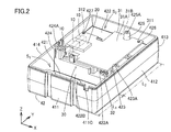
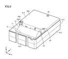
- FIG. 3 is a schematic perspective view showing the structure of the wireless terminal device according to the first embodiment. It is a schematic perspective view which shows the structure of the wireless terminal device in the state which removed the 1st upper wall part and the 2nd upper wall part. It is a schematic perspective view which shows the structure of the wireless terminal device in the state which removed the 1st upper wall part and the 2nd upper wall part. It is a schematic perspective view which shows the structure of the wireless terminal device in the state which removed the 1st upper wall part.
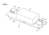
- FIG. 3 is a schematic perspective view showing the structure of the external power supply module in the first embodiment. It is a schematic perspective view which shows the state which the external power supply module was attached to the 1st upper wall part.
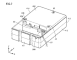
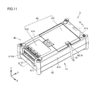
- FIG. 6 is a schematic perspective view showing the structure of a wireless terminal device according to a second embodiment. It is a schematic perspective view which shows the structure of the wireless terminal device in the state which removed the 1st upper wall part. It is a schematic perspective view which shows the structure of the wireless terminal device in the state which removed the 1st upper wall part and the external power supply module.
- FIG. 6 is a schematic perspective view showing the structure of a wireless terminal device according to a second embodiment. It is a schematic perspective view which shows the structure of the wireless terminal device in the state which removed the 1st upper wall part. It is a schematic perspective view which shows the structure of the wireless terminal device in the state which removed the 1st upper wall part and the external power supply module.
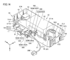
- FIG. 9 is a schematic perspective view showing the structure of the external power supply module in the second embodiment. It is a schematic sectional drawing which shows the state with which the external power supply module was attached.
- FIG. 6 is a schematic perspective view showing a configuration of a battery attached to the wireless terminal device according to the second embodiment.
- the wireless terminal device may be installed on a trial basis in a factory or the like.
- the installation location of the wireless terminal device may be changed to consider an appropriate installation location.
- the wireless terminal device is preferably driven by a battery in consideration of ease of installation and removal.
- a wireless terminal device of the present application includes an input unit that receives an input from a sensor, an output unit that converts a signal input from the sensor to the input unit into a wireless signal and outputs the wireless signal, and electrically connects the input unit and the output unit.
- Circuit board module and an external power supply that is detachably connected to the circuit board module and that includes an input terminal that receives an input from an external power supply and that converts the input voltage input to the input terminal to output the output voltage.
- a module and a storage space for storing the external power supply module are formed, and the module includes a case that houses the input unit, the output unit, the circuit board module, and the external power supply module.
- a battery can be stored in the storage space by removing the external power supply module from the circuit board module.
- the circuit board module can selectively connect either one of the connector of the external power supply module and the connector of the battery, and includes a connector connecting portion arranged at a position spatially connected to the storage space.
- the wireless terminal device of the present application includes an external power supply module stored in the storage space. Further, the storage space can store the battery by removing the external power supply module.
- the circuit board module in the wireless terminal device of the present application includes a connector connecting portion arranged at a position spatially connected to the storage space. With such a configuration, the connector of the external power supply module and the connector of the battery can be easily replaced. Therefore, it is possible to drive the wireless terminal device by using the external power source, attach the battery, and drive the wireless terminal device by the battery. Therefore, according to the wireless terminal device of the present application, it can be driven not only by using the external power source but also by the battery.
- the case of the wireless terminal device may include a holding portion that is arranged in the storage space and has a cylindrical holding surface that can hold the battery. With such a configuration, it is possible to properly hold the battery in the storage space and regulate the movement of the battery.
- the case of the wireless terminal device may be formed with an opening that connects the storage space and the external space and has a shape that allows the external power supply module and the battery arranged in the storage space to be taken out.
- the case may include a lid that is arranged to be able to close and open the opening.
- the external power supply module is disposed on the first main surface and a substrate having a first main surface and a second main surface located on the side opposite to the first main surface in the thickness direction, and is input to an input terminal from an external power supply. And a conversion unit that converts an input voltage and outputs an output voltage.
- the external power supply module may be stored in the storage space so that the second main surface faces the lid portion. With such a configuration, it is possible to prevent an operator from touching the conversion unit and damaging the conversion unit.
- the case of the wireless terminal device may be formed with an opening that connects the storage space and the external space and has a shape that allows the external power supply module and the battery arranged in the storage space to be taken out.
- the case may include a lid part that can close and open the opening part, and a holding part that is arranged in the storage space and has a cylindrical holding surface that can hold the battery.
- the external power supply module is disposed on the first main surface and a substrate having a first main surface and a second main surface located on the side opposite to the first main surface in the thickness direction, and is input to an input terminal from an external power supply. And a conversion unit that converts an input voltage and outputs an output voltage.
- the first main surface of the substrate may face the holding surface. With such a configuration, the space inside the cylindrical holding surface can be effectively used to store the conversion unit arranged on the substrate.
- the case of the wireless terminal device may be formed with a through hole having a shape through which an external wire connecting the input terminal and the external power supply can be inserted.
- the external wiring can be easily taken out of the case by inserting the external wiring into the through hole.
- the wireless terminal device may further include a first member that is disposed inside the case and that has a first protrusion that protrudes in the first direction.
- External wiring that connects the input terminal and the external power supply may be wound so as to come into contact with the outer peripheral surface of the first protrusion. With such a configuration, the movement of the external wiring can be restricted by the first protrusion. Therefore, it becomes easy to fix the external wiring in the case.
- the external wiring may be wound so as to extend over more than a half circumference in the circumferential direction of the first protrusion.
- the wireless terminal device may further include a second member that is disposed inside the case and that has a second protrusion that protrudes in the second direction.
- External wiring extending from the external power supply module may be wound so as to come into contact with the outer peripheral surface of the first protrusion.
- An external wire extending from the first protrusion may be wound so as to come into contact with the outer peripheral surface of the second protrusion.
- the angle formed by the first direction and the second direction may be 90 degrees or less when viewed two-dimensionally in a direction perpendicular to a plane including the straight line.
- the external wiring is viewed two-dimensionally in a direction perpendicular to a plane including a third straight line along a third direction from the second protruding portion toward a side different from the first protruding portion side and the second straight line.
- the angle formed by the second direction and the third direction may be 90 degrees or less.
- FIG. 2 is a perspective view corresponding to a state in which the first upper wall portion and the second upper wall portion of FIG. 1 are removed.
- FIG. 3 is a schematic perspective view showing the structure of the wireless terminal device viewed from a different viewpoint from FIG. 8 and 10 are cross-sectional views taken along the line segment AA in FIG.
- the Z-axis direction is the direction along the thickness direction of the first upper wall portion.
- the direction along the long side of the case having a rectangular shape when viewed two-dimensionally in the Z-axis direction is the Y-axis direction
- the direction along the short side is the X-axis direction.
- the wireless terminal device 1 includes a case 40, an input unit 10, an output unit 20, a circuit board module 30, and an external power supply module 50.
- the case 40 has a rectangular parallelepiped shape in which an internal space is formed.
- the case 40 includes a hollow tubular side wall portion 41, a bottom wall portion 42, and an upper wall portion 43.
- the bottom wall portion 42 is arranged so as to close one opening of the side wall portion 41.
- the upper wall portion 43 is arranged so as to close the other opening of the side wall portion 41.
- the side wall portion 41 includes a first side wall portion 411, a second side wall portion 412, a third side wall portion 413, and a fourth side wall portion 414.
- the first side wall portion 411, the second side wall portion 412, the third side wall portion 413, and the fourth side wall portion 414 have a flat plate shape.
- the first side wall part 411 and the third side wall part 413 are arranged in parallel in the Y-axis direction with a space therebetween.
- the second side wall portion 412 and the fourth side wall portion 414 are arranged in parallel in the X-axis direction at intervals.
- One end of the first side wall portion 411 in the X-axis direction is connected to the second side wall portion 412.
- the other end of the first side wall portion 411 in the X-axis direction is connected to the fourth side wall portion 414.
- One end of the third side wall part 413 in the X-axis direction is connected to the second side wall part 412.
- the other end of the third side wall part 413 in the X-axis direction is connected to the fourth side wall part 414.
- the first side wall portion 411 is arranged so that the angle formed by the second side wall portion 412 and the fourth side wall portion 414 is a right angle.
- the third side wall portion 413 is arranged so that an angle formed by the second side wall portion 412 and the fourth side wall portion 414 is a right angle when seen in a plan view in the Z-axis direction.
- the side wall portion 41 has a rectangular shape when seen in a plan view in the Z-axis direction.
- the first side wall part 411 and the third side wall part 413 correspond to the short sides.
- the second side wall portion 412 and the fourth side wall portion 414 correspond to the long side.
- a notch 411C is formed in a region of the end surface on the upper wall 43 side of the first side wall 411 closer to the second side wall 412 than the center in the X-axis direction.
- the notch 411C has a shape through which an external wiring 61 described later can be inserted.
- the notch 411C forms a through hole by attaching the first upper wall portion 431.
- a through hole 414A penetrating in the thickness direction is formed at the end portion of the fourth side wall portion 414 on the bottom wall portion 42 side and slightly on the third side wall portion 413 side from the center in the Y-axis direction.
- the bottom wall portion 42 has a flat plate shape.
- the bottom wall portion 42 has a rectangular shape when seen in a plan view in the Z-axis direction.
- the bottom wall portion 42 is connected to the side wall portion 41 on the outer circumference thereof.
- the bottom wall portion 42 includes a first region 421 and a second region 422.
- the length L 1 of the first region 421 in the Y-axis direction is shorter than the length L 2 of the second region 422 in the Y-axis direction.
- protrusions 426 and 427 that project in the thickness direction of the bottom wall portion 42 are formed.
- the second region 422 is a region that is thicker than the first region 421. That is, the height of the inner wall surface of the first region 421 in the Z-axis direction is lower than the height of the inner wall surface of the second region 422 in the Z-axis direction.
- the distance between the first region 421 and the second upper wall portion 432 in the Z-axis direction is larger than the distance between the second region 422 and the second upper wall portion 432 in the Z-axis direction. Therefore, a step portion 422B is formed between the first region 421 and the second region 422.
- the first region 421 and the second region 422 each have a rectangular shape when viewed in plan in the Z-axis direction.
- the first region 421 and the second region 422 are arranged so as to be continuous in the Y-axis direction.
- a cylindrical first holding surface 421A extending in the X-axis direction is formed in a region of the first region 421 on the first side wall portion 411 side.
- the first holding surface 421A has a shape capable of holding a cylindrical battery.
- a recess 422A is formed on the end portion on the first region 421 side and on the second side wall portion 412 side with respect to the center in the X-axis direction.
- the region of the second region 422 in which the recess 422A is formed is a region having a larger thickness than the first region 421. That is, the height of the inner wall surface of the first region 421 in the Z-axis direction is lower than the height of the inner wall surface of the region of the second region 422 in which the recess 422A is formed in the Z-axis direction.
- the distance between the first region 421 and the second upper wall portion 432 in the Z-axis direction is the same as that of the second region 422 in which the recess 422A is formed and the second upper wall portion 432. Is greater than the distance in the Z-axis direction.
- the thickness of the recess 422A is smaller than the thickness of the second region 422 in the region other than the recess 422A. That is, the distance between the recess 422A and the second upper wall portion 432 is larger than the distance between the second region 422 and the second upper wall portion 432 in the region other than the recess 422A.
- the first pillar portion 423 is an end portion of the second region 422 on the first region 421 side and is arranged at a position in contact with the second side wall portion 412.
- the second pillar portion 424 is an end portion of the second region 422 on the first region 421 side and is arranged at a position in contact with the fourth side wall portion 414.
- the third pillar portion 425 is an end portion of the second region 422 on the third side wall portion 413 side, and is arranged at a position closer to the second side wall portion 412 than the center in the X-axis direction.
- the first pillar portion 423 has a cylindrical shape.
- a screw hole 423A surrounded by a spiral wall surface is formed so as to include the central axis of the first column portion 423.
- the second pillar portion 424 has a prismatic shape.
- a screw hole 424A surrounded by a spiral wall surface is formed so as to include the central axis of the second column portion 424.
- the third pillar portion 425 has a cylindrical shape.
- a screw hole 425A surrounded by a spiral wall surface is formed so as to include the central axis of the third column portion 425.
- the first protrusion 426 is arranged between the third pillar 425 and the second side wall 412 in the X-axis direction.
- the second protrusion 427 is arranged between the second pillar 424 and the third side wall 413 in the Y-axis direction.
- the first protrusion 426 and the second protrusion 427 have a cylindrical shape.
- the upper wall portion 43 includes a first upper wall portion 431 as a lid portion and a second upper wall portion 432.
- the second upper wall portion 432 has a flat plate shape.
- the second upper wall portion 432 has a rectangular shape when seen in a plan view in the Z-axis direction.
- the second upper wall portion 432 is formed with a screw hole 433 penetrating in the thickness direction so as to correspond to the screw hole 423A of the first column portion 423.
- the second upper wall portion 432 is formed with a screw hole 434 penetrating in the thickness direction so as to correspond to the screw hole 424A of the second column portion 424.
- the second upper wall portion 432 is formed with a screw hole 435 penetrating in the thickness direction so as to correspond to the screw hole 425A of the third column portion 425.
- a recess 436 that is a portion having a small thickness is formed.
- the screw 45 is screwed in with the second upper wall portion 432 placed on the side wall portion 41 so that the position where the screw hole 433 is formed and the position where the screw hole 423A is formed match.
- the screw 46 is Screwed in. In this way, the second upper wall portion 432 is fixed to the bottom wall portion 42 (second region 422).
- the first upper wall portion 431 includes a claw portion 438 protruding toward the second upper wall portion 432.
- the inner wall surface 437A of the first upper wall portion 431 is provided with third protrusions 441 and 442 protruding in the thickness direction.
- claw portions 443 and 444 protruding in the thickness direction are formed on the inner wall surface 437A of the first upper wall portion 431.
- a cylindrical second holding surface 445 extending along the X-axis direction is formed closer to the second upper wall portion 432 than the center of the inner wall surface 437A in the Y-axis direction.
- the second holding surface 445 has a shape capable of holding a cylindrical battery.
- the claw portion 438 has a shape corresponding to the concave portion 436.
- a concave portion 438A is formed in the claw portion 438 at a position corresponding to the screw hole 434.
- the claw portion 438 is fitted into the concave portion 436, and the screw 44 is screwed in with the first upper wall portion 431 arranged such that the position where the screw hole 434 is formed and the position where the concave portion 438A is formed match. .. In this way, the first upper wall portion 431 is held by the side wall portion 41. By removing the screw 44, the first upper wall portion 431 can be removed. Therefore, the first upper wall portion 431 functions as a lid portion.
- a first member 446 is arranged near one corner on the second upper wall 432 side of the inner wall surface 437A of the first upper wall 431 having a rectangular shape when seen in a plan view in the Z-axis direction.
- the second member 447 is arranged near the other corner of the inner wall surface 437A of the first upper wall portion 431 on the second upper wall portion 432.
- the third member 448 is arranged on the side where the second member 447 is arranged and near the corner on the first side wall portion 411 side. That is, the first member 446 and the second member 447 are arranged side by side along the long side of the first upper wall portion 431 with an interval.
- the second member 447 and the third member 448 are arranged side by side along the short side of the first upper wall portion 431 with an interval.
- the first member 446 and the second member 447 include a first protrusion 446A and a second protrusion 447A protruding in the Z-axis direction, and a first claw 446B and a second claw 447B extending in the Y-axis direction.
- the first claw portion 446B and the second claw portion 447B are arranged continuously from the ends of the first projecting portion 446A and the second projecting portion 447A opposite to the first upper wall portion 431 side.
- the third member 448 includes a third protrusion 448A protruding in the Z-axis direction and a third claw portion 448B extending in the X-axis direction.
- the third claw portion 448B is arranged continuously from the end of the third protruding portion 448A on the opposite side to the first upper wall portion 431.
- a space S 2 surrounded by the second side wall portion 412, the third side wall portion 413, the fourth side wall portion 414, the second region 422, and the second upper wall portion 432 is formed in the case 40.
- the circuit board module 30 is arranged on the second region 422.
- the circuit board module 30 includes a first board 31 and a connector connecting portion 32.
- the first substrate 31 has a flat plate shape.
- the first substrate 31 has through holes 311 and 312 penetrating in the thickness direction at positions corresponding to the first protrusions 426 and the second protrusions 427.
- the first projecting portion 426 and the second projecting portion 427 are inserted into the through holes 311 and 312 to fix the first substrate 31 to the second region 422.
- the first substrate 31 has a first main surface 31A facing the second upper wall portion 432 and a second main surface 31B opposite to the first main surface 31A side. 2 and 3, connector connecting portion 32 is arranged on second main surface 31B.
- the connector connecting portion 32 is a connecting portion to which the external power supply module 50 and the battery connector are connected.
- the connector connecting portion 32 is arranged at a position corresponding to the recess 422A of the second region 422. Therefore, the connector connecting portion 32 is arranged at a position spatially connected to the space S 1 .
- the input unit 10 receives an input from the sensor.
- the input unit 10 is composed of three input units.
- the input unit 10 is arranged on the second main surface 31B of the first substrate 31 and is electrically connected to the circuit board module 30.
- the input unit 10 is arranged so as to be accessible from the external space via the through hole 414A of the fourth side wall unit 414.
- the output unit 20 converts a signal from the sensor input to the input unit 10 into a wireless signal and outputs the wireless signal.
- the output unit 20 is arranged on the first main surface 31A of the first substrate 31 and is electrically connected to the circuit board module 30.
- the external power supply module 50 is a module that converts an input voltage from an external power supply and outputs an output voltage.
- the external power supply module 50 includes a second substrate 51, a conversion unit 52, an input terminal 53, and an output terminal 54.
- the second substrate 51 has a flat plate shape.
- the second substrate 51 has a substantially rectangular shape when viewed two-dimensionally in the thickness direction (Z-axis direction).
- the second substrate 51 has a first main surface 51A on one side and a second main surface 51B located on the opposite side of the first main surface 51A in the thickness direction.
- Through holes 511 and 512 penetrating in the thickness direction are formed in the second substrate 51 at positions corresponding to the third protrusions 441 and 442.
- the third protrusions 441 and 442 are inserted into the through holes 511 and 512, and the claws 443 and 444 fix the second substrate 51 to the first upper wall 431.
- the first main surface 51A is arranged so as to face the first region 421.
- the first main surface 51A is arranged so as to face the first holding surface 421A.
- the second main surface 51B is arranged so as to face the inner wall surface 437A of the first upper wall portion 431.
- the input terminal 53 is a terminal that receives an input from an external power supply.
- the converter 52 converts the input voltage input to the input terminal 53 into a desired voltage.
- the output terminal 54 is a terminal that outputs the output voltage converted by the conversion unit 52.
- the converter 52, the input terminal 53, and the output terminal 54 are arranged on the first main surface 51A.
- the converter 52, the input terminal 53, and the output terminal 54 are arranged along the X-axis direction.
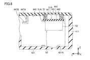
- the output terminal 54 is arranged on the side opposite to the side on which the input terminal 53 is arranged as viewed from the conversion section 52. Referring to FIG. 8, conversion unit 52 is arranged so as to face first holding surface 421A.
- the input terminal 53 has a shape to which the connector 62 of the external wiring 61 can be connected.
- a connector 58A is arranged at one end of the internal wiring 57, and a connector 58B is arranged at the other end.
- the connector 58A has a shape connectable to the output terminal 54.
- the connector 58B has a shape connectable to the connector connecting portion 32 (see FIGS. 2 and 7).
- the external power supply and the external power supply module 50 are electrically connected.
- the external power supply module 50 and the circuit board module 30 are electrically connected by connecting the connector 58A to the output terminal 54 and connecting the connector 58B to the connector connecting portion 32.
- the external wiring 61 is inserted into the notch 411C of the first side wall portion 411 and is drawn out to the external space (see particularly FIG. 1).
- batteries 71 and 72 can be stored in space S 1 as a storage space.
- two cylindrical batteries are stored.
- the battery 71 is held so that the outer peripheral surface of the battery 71 contacts the first holding surface 421A.
- the battery 72 is held so that the outer peripheral surface of the battery 72 contacts the second holding surface 445. That is, the first region 421 of the bottom wall portion 42 and the first upper wall portion 431 function as a holding portion that holds the batteries 71 and 72.
- the space S 1 can store the batteries 71 and 72 by removing the external power supply module 50.
- the circuit board module 30 includes a connector connecting portion 32 arranged at a position spatially connected to the space S 1 .
- the case 40 is arranged in the space S 1 and has the cylindrical first holding surface 421A and the second holding surface 445 capable of holding the battery.
- the batteries 71 and 72 can be properly held in the space S 1 and movement of the batteries 71 and 72 can be restricted.
- the opening S 3 is formed.
- the external power supply module 50 and the batteries 71 and 72 arranged in the space S 1 can be taken out from the opening S 3 .
- the external wiring 61 is wound so as to exceed a half circumference in the circumferential direction of the first protrusion 446A.
- external wiring 61 extending from external power supply module 50 is wound so as to come into contact with the outer peripheral surface of first protrusion 446A.
- the external wiring 61 extending from the first protrusion 446A is wound so as to come into contact with the outer peripheral surface of the second protrusion 447A.
- the external wiring 61 extending from the second protrusion 447A is held by the third member 448 and extends to the external space.
- the first straight line along which the external wiring 61 extends from the external power supply module 50 toward the first protruding portion 446A along the first direction L1 and the second external wiring 61 extends from the first protruding portion 446A toward the second protruding portion 447A.
- the angle formed by the second direction L 2 and the third direction L 3 is 90 degrees or less.
- the wireless terminal device 1 according to the second embodiment has basically the same structure as the wireless terminal device 1 according to the first embodiment and has the same effect.
- the second embodiment is different from the first embodiment in the structure of the holding portion for holding the battery.
- differences from the first embodiment will be mainly described.
- FIG. 12 is a perspective view corresponding to a state in which the first upper wall portion 431 as the lid portion of FIG. 11 is removed.
- FIG. 13 is a perspective view corresponding to a state in which the first upper wall portion 431 as the lid portion and the external power supply module 50 of FIG. 11 are removed.
- FIG. 15 is a sectional view taken along the line BB in FIG.
- the case 40 includes a side wall portion 41, a bottom wall portion 42, an upper wall portion 43, and a holding portion 43A.
- the upper wall portion 43 includes a first upper wall portion 431 and a second upper wall portion 432.
- a notch 481A is formed in the first upper wall portion 431 at the end on the second side wall portion 412 side and in the center in the Y-axis direction.
- the notch 481A forms a through hole by attaching the first upper wall portion 431 to the case 40.
- the notch 481A has a shape into which the external wiring 61 can be inserted.
- the holding portion 43A is arranged so as to correspond to the first upper wall portion 431 when seen in a plan view in the Z-axis direction.
- Holding portion 43A includes a bottom wall portion 42, the second side wall portion 412, a third side wall portion 413, is disposed in the fourth storage space S 1 surrounded by the side wall portion 414 and the first upper wall portion 431.
- the holding portion 43A is connected to the second upper wall portion 432 by the connecting portion 455.
- the holding portion 43A has a third holding surface 456 that is recessed in a cylindrical shape.
- the third holding surface 456 has a shape capable of holding the cylindrical battery 74 (see especially FIG. 16).
- a claw portion 453B protruding along the Y-axis direction is formed on the holding portion 43A.
- the holding portion 43A is formed with a through hole 453A extending in the X-axis direction along the claw portion 453B.
- the input unit 10 of the circuit board module 30 is arranged so as to be exposed from the recess 411A extending from the center of the first side wall 411 in the X-axis direction to the second upper wall 432.
- the connector connecting portion 32 of the circuit board module 30 is arranged so as to be exposed from the through hole 455A formed in the connecting portion 455.
- the external power supply module 50 includes a second substrate 51, a converter 52, an input terminal 53, an output terminal 54, and a holding member 59.
- the holding member 59 is a member that holds the second substrate 51.
- the holding member 59 includes a side wall portion 55 and a bottom lid portion 56.
- the side wall portion 55 includes a first portion 571, a second portion 572, a third portion 573, and a fourth portion 574.
- the first portion 571 to the fourth portion 574 have a plate shape.
- the first portion 571 and the third portion 573 are arranged in parallel in the Y-axis direction with a space therebetween.
- the second portion 572 and the fourth portion 574 are arranged in parallel with each other with a space in the X-axis direction.
- the first portion 571 is connected to one end of the second portion 572 in the Y-axis direction.
- the third portion 573 is connected to the other end of the second portion 572 in the Y-axis direction.
- the third portion 573 is connected to one end of the fourth portion 574 in the Y-axis direction.
- the second portion 572 is arranged so that an angle formed by the first portion 571 and the third portion 573 is a right angle when seen in a plan view in the Z-axis direction.
- the fourth portion 574 is arranged so that an angle formed by the fourth portion 574 and the third portion 573 is a right angle when seen in a plan view in the Z-axis direction.
- a first cutout portion 571A penetrating in the thickness direction is formed on an end portion of the first portion 571 opposite to the bottom lid portion 56 and on the second portion 572 side from the center in the X-axis direction. ..
- the first cutout portion 571A has a shape that allows the internal wiring 57 to be inserted therethrough.
- a second cutout portion 571B penetrating in the thickness direction is formed on an end portion of the first portion 571 opposite to the bottom lid portion 56 and on the fourth portion 574 side from the center in the X-axis direction. ..
- the second cutout portion 571B has a shape that allows the external wiring 61 to be inserted therethrough.
- the first member 591, the second member 592, the third member 593, the fourth member 594, the fifth member 595, and the sixth member 596 are arranged on the outer wall surface of the first portion 571. There is.
- the second member 592 and the fourth member 594 are arranged along the X-axis direction.
- the first member 591, the third member 593, and the fifth member 595 are arranged along the X-axis direction.
- the sixth member 596 is arranged on the side opposite to the bottom lid portion 56 side in the Z-axis direction when viewed from the second member 592 and the fourth member 594.
- the first member 591, the second member 592, the third member 593, the fourth member 594, the fifth member 595, and the sixth member 596 respectively have a first protrusion 591A, a second protrusion 592A, and a second protrusion 592A that protrude in the Y-axis direction.
- the fourth claw portion 594B, the fifth claw portion 595B, and the sixth claw portion 596B are included.
- the first claw portion 591B, the second claw portion 592B, the third claw portion 593B, the fourth claw portion 594B, the fifth claw portion 595B, and the sixth claw portion 596B include a first projecting portion 591A, a second projecting portion 592A, and a fifth projecting portion 592A.
- the third protruding portion 593A, the fourth protruding portion 594A, the fifth protruding portion 595A, and the sixth protruding portion 596A are arranged so as to be continuous from the end portion on the side opposite to the first portion 571 side.
- the external wiring 61 is held by the first member 591, the second member 592, and the third member 593, and is wound around the fourth member 594.
- the external wiring 61 is wound so as to extend over a half circumference in the circumferential direction of the fourth protrusion 594A of the fourth member 594.
- the external wiring 61 is inserted into the cutout 481A of the first upper wall portion 431 and is drawn out to the external space (see particularly FIG. 11).
- the internal wiring 57 is held by the sixth member 596 and wound around the fifth protruding portion 595A of the fifth member 595.
- the columnar portions 561 and 562 formed on the bottom lid portion 56 are inserted into the through holes 511 and 512 of the second substrate 51, and the second substrate 51 is arranged in the space surrounded by the side wall portion 55.
- the second substrate 51 is held by the first portion 571, the second portion 572, the third portion 573, and the fourth portion 574.
- the converter 52, the input terminal 53, and the output terminal 54 are arranged on the first main surface 51A of the second substrate 51.
- the external power supply module 50 is arranged so as to face the third holding surface 456 of the holding portion 43A.
- the external power supply module 50 is arranged so that the fourth protrusion 573A of the holding member 59 is inserted into the through hole 453A of the holding portion 43A.
- the first main surface 51A of the second substrate 51 is arranged so as to face the third holding surface 456.
- the battery 74 when external power supply module 50 is removed, battery 74 can be stored in space S 1 as a storage space.
- the battery 74 includes a main body portion 741 having a cylindrical shape, wirings 742A and 742B, and a connector 73.
- the wirings 742A and 742B are electrically connected to the electrodes of the main body portion 741.
- the connector 73 is connected to the ends of the wirings 742A and 742B on the side opposite to the main body 741.
- the battery 74 and the circuit board module 30 are electrically connected.
- the battery 74 is held so that the outer peripheral surface 741A of the main body portion 741 contacts the third holding surface 456. That is, the holding unit 43A functions as a holding unit that holds the battery 74.
- the circuit board module 30 includes the connector connecting portion 32 arranged at a position spatially connected to the space S 1 .
- the connector 58B of the external power supply module 50 and the connector 73 of the battery 74 can be easily replaced. Therefore, the wireless terminal device 1 according to the second embodiment can be driven by using the external power source as well as by the battery, as in the first embodiment.
Landscapes
- Engineering & Computer Science (AREA)
- Microelectronics & Electronic Packaging (AREA)
- Automation & Control Theory (AREA)
- Computer Networks & Wireless Communication (AREA)
- Signal Processing (AREA)
- Telephone Set Structure (AREA)
- Transmitters (AREA)
Abstract
無線端末装置は、入力部と、出力部と、入力部および出力部と電気的に接続された回路基板モジュールと、回路基板モジュールと着脱可能に接続されており、外部電源からの入力を受ける入力端子を含み、入力端子に入力される入力電圧を変換して出力電圧を出力する外部電源モジュールと、入力部、出力部、回路基板モジュールおよび外部電源モジュールを収容するケースと、を備える。格納空間は、外部電源モジュールを回路基板モジュールから取り外すことにより、電池を格納可能である。回路基板モジュールは、外部電源モジュールのコネクタ、および電池のコネクタのうちいずれか一方を選択的に接続可能であって、格納空間から空間的につながった位置に配置されたコネクタ接続部を含む。
Description
本発明は、無線端末装置に関するものである。
特許文献1には、加速度センサ等の振動を検出可能な振動センサと、検出された振動信号を外部機器に無線で送信する送信装置と、を備える無線端末装置を操業中の設備に取り付け、設備の異常が判断されることが開示されている。
本開示の無線端末装置は、センサからの入力を受ける入力部と、入力部に入力されたセンサからの信号を無線信号に変換して出力する出力部と、入力部および出力部と電気的に接続された回路基板モジュールと、回路基板モジュールと着脱可能に接続されており、外部電源からの入力を受ける入力端子を含み、入力端子に入力される入力電圧を変換して出力電圧を出力する外部電源モジュールと、外部電源モジュールを格納する格納空間が形成されており、入力部、出力部、回路基板モジュールおよび外部電源モジュールを収容するケースと、を備える。格納空間は、外部電源モジュールを回路基板モジュールから取り外すことにより、電池を格納可能である。回路基板モジュールは、外部電源モジュールのコネクタ、および電池のコネクタのうちいずれか一方を選択的に接続可能であって、格納空間から空間的につながった位置に配置されたコネクタ接続部を含む。
[本開示が解決しようとする課題]
無線端末装置は、工場内等に試験的に設置される場合がある。また、無線端末装置の設置場所を変更して、適切な設置場所を検討する場合がある。このような場合、設置および取り外しの容易性を考慮して、無線端末装置は、電池によって駆動されることが好ましい。しかしながら、無線端末装置が恒久的に設置されることとなった場合や設置位置が確定した後は、継続的に工場内に設置される外部電源を用いて駆動されることが好ましい。そこで、外部電源を利用して駆動させることができると共に、電池によっても駆動させることができる無線端末装置を提供することを目的の1つとする。
無線端末装置は、工場内等に試験的に設置される場合がある。また、無線端末装置の設置場所を変更して、適切な設置場所を検討する場合がある。このような場合、設置および取り外しの容易性を考慮して、無線端末装置は、電池によって駆動されることが好ましい。しかしながら、無線端末装置が恒久的に設置されることとなった場合や設置位置が確定した後は、継続的に工場内に設置される外部電源を用いて駆動されることが好ましい。そこで、外部電源を利用して駆動させることができると共に、電池によっても駆動させることができる無線端末装置を提供することを目的の1つとする。
[本開示の効果]
本開示によれば、外部電源を利用して駆動させることができると共に、電池によっても駆動させることができる無線端末装置を提供することができる。
本開示によれば、外部電源を利用して駆動させることができると共に、電池によっても駆動させることができる無線端末装置を提供することができる。
[本願発明の実施形態の説明]
最初に本願発明の実施態様を列記して説明する。本願の無線端末装置は、センサからの入力を受ける入力部と、入力部に入力されたセンサからの信号を無線信号に変換して出力する出力部と、入力部および出力部と電気的に接続された回路基板モジュールと、回路基板モジュールと着脱可能に接続されており、外部電源からの入力を受ける入力端子を含み、入力端子に入力される入力電圧を変換して出力電圧を出力する外部電源モジュールと、外部電源モジュールを格納する格納空間が形成されており、入力部、出力部、回路基板モジュールおよび外部電源モジュールを収容するケースと、を備える。格納空間は、外部電源モジュールを回路基板モジュールから取り外すことにより、電池を格納可能である。回路基板モジュールは、外部電源モジュールのコネクタ、および電池のコネクタのうちいずれか一方を選択的に接続可能であって、格納空間から空間的につながった位置に配置されたコネクタ接続部を含む。
最初に本願発明の実施態様を列記して説明する。本願の無線端末装置は、センサからの入力を受ける入力部と、入力部に入力されたセンサからの信号を無線信号に変換して出力する出力部と、入力部および出力部と電気的に接続された回路基板モジュールと、回路基板モジュールと着脱可能に接続されており、外部電源からの入力を受ける入力端子を含み、入力端子に入力される入力電圧を変換して出力電圧を出力する外部電源モジュールと、外部電源モジュールを格納する格納空間が形成されており、入力部、出力部、回路基板モジュールおよび外部電源モジュールを収容するケースと、を備える。格納空間は、外部電源モジュールを回路基板モジュールから取り外すことにより、電池を格納可能である。回路基板モジュールは、外部電源モジュールのコネクタ、および電池のコネクタのうちいずれか一方を選択的に接続可能であって、格納空間から空間的につながった位置に配置されたコネクタ接続部を含む。
本願の無線端末装置は、格納空間に格納された外部電源モジュールを備える。また、格納空間は、外部電源モジュールを取り外すことにより、電池を格納可能である。そして、本願の無線端末装置における回路基板モジュールは、格納空間から空間的につながった位置に配置されたコネクタ接続部を含む。このような構成とすることで、外部電源モジュールのコネクタと、電池のコネクタとを容易に付け替えることができる。そのため、外部電源を利用して、無線端末装置を駆動することが可能であるとともに、電池を取り付けて、電池により無線端末装置を駆動することが可能である。したがって、本願の無線端末装置によれば、外部電源を利用して駆動させることができると共に、電池によっても駆動させることができる。
上記無線端末装置におけるケースは、格納空間に配置され、電池を保持可能な円筒面状の保持面を有する保持部を含んでもよい。このような構成とすることで、格納空間において電池を適切に保持し、電池が移動することを規制することができる。
上記無線端末装置におけるケースには、格納空間と外部空間とを繋ぎ、格納空間に配置される外部電源モジュールおよび電池を取り出し可能な形状を有する開口部が形成されてもよい。ケースは、開口部を閉塞および開放可能に配置される蓋部を含んでもよい。外部電源モジュールは、第1主面および第1主面とは厚み方向において反対側に位置する第2主面を有する基板と、第1主面上に配置され、外部電源から入力端子に入力される入力電圧を変換して出力電圧を出力する変換部と、を含んでもよい。外部電源モジュールは、第2主面が蓋部に対向するように格納空間に格納されてもよい。このような構成とすることで、作業者が変換部に触れて、変換部に損傷を与えることを抑制することができる。
上記無線端末装置におけるケースには、格納空間と外部空間とを繋ぎ、格納空間に配置される外部電源モジュールおよび電池を取り出し可能な形状を有する開口部が形成されてもよい。ケースは、開口部を閉塞および開放可能に配置される蓋部と、格納空間に配置され、電池を保持可能な円筒面状の保持面を有する保持部と、を含んでもよい。外部電源モジュールは、第1主面および第1主面とは厚み方向において反対側に位置する第2主面を有する基板と、第1主面上に配置され、外部電源から入力端子に入力される入力電圧を変換して出力電圧を出力する変換部と、を含んでもよい。基板の第1主面は、保持面と対向してもよい。このような構成とすることで、円筒面状の保持面の内側の空間を有効に利用して、基板上に配置される変換部を格納することができる。
上記無線端末装置におけるケースには、入力端子と外部電源とを接続する外部配線が挿通可能な形状を有する貫通孔が形成されてもよい。このような構成とすることで、上記貫通孔に外部配線を挿通させて、外部配線をケースの外部に容易に取り出すことができる。
上記無線端末装置は、ケースの内部に配置され、第1の向きに突出する第1突出部を有する第1部材をさらに備えてもよい。第1突出部の外周面と接触するように、入力端子と外部電源とを接続する外部配線が巻き付けられてもよい。このような構成とすることで、外部配線の移動を第1突出部により規制することができる。したがって、外部配線をケース内において固定することが容易となる。
上記無線端末装置において、外部配線は、第1突出部の周方向において半周を超えるように巻き付けられてもよい。このような構成とすることで、外部配線が引っ張られた際に、外部電源モジュールと第1突出部との間において、外部配線を引っ張る力が低減される。したがって、外部配線が引っ張られたとしても、外部配線の入力端子への接続部付近が受ける損傷を抑制することができる。
上記無線端末装置は、ケースの内部に配置され、第2の向きに突出する第2突出部を有する第2部材をさらに備えてもよい。第1突出部の外周面と接触するように、外部電源モジュールから延びる外部配線が巻き付けられてもよい。第2突出部の外周面と接触するように、第1突出部から延びる外部配線が巻き付けられてもよい。外部配線が外部電源モジュールから第1突出部に向かう第1の方向に沿った第1の直線と、外部配線が第1突出部から第2突出部に向かう第2の方向に沿った第2の直線と、を含む平面に垂直な方向に平面的に見て、第1の方向と、第2の方向とのなす角度が90度以下であってもよい。外部配線が第2突出部から第1突出部側とは異なる側に向かう第3の方向に沿った第3の直線と、第2の直線と、を含む平面に垂直な方向に平面的に見て、第2の方向と、第3の方向とのなす角度が90度以下であってもよい。このような構成とすることで、外部配線が引っ張られた際に、第1突出部と第2突出部との間において、外部配線を引っ張る力が低減される。さらに、外部電源モジュールと第1突出部との間において、外部配線を引っ張る力がさらに低減される。したがって、外部配線が引っ張られたとしても、外部配線の入力端子への接続部付近が受ける損傷をさらに抑制することができる。
[本願発明の実施形態の詳細]
次に、本願の無線端末装置の一実施の形態を、図面を参照しつつ説明する。以下の図面において同一または相当する部分には同一の参照番号を付しその説明は繰返さない。
次に、本願の無線端末装置の一実施の形態を、図面を参照しつつ説明する。以下の図面において同一または相当する部分には同一の参照番号を付しその説明は繰返さない。
(実施の形態1)
まず、図1~図10を参照して実施の形態1について説明する。図2は、図1の第1上壁部および第2上壁部を取り外した状態に対応する斜視図である。図3は、図2とは異なる視点から見た無線端末装置の構造を示す概略斜視図である。図8および図10は、図1の線分A-Aに沿って切断した場合の断面図である。図1において、Z軸方向は、第1上壁部の厚み方向に沿った方向である。Z軸方向に平面的に見た時の長方形状を有するケースの長辺に沿った方向がY軸方向であり、短辺に沿った方向がX軸方向である。
まず、図1~図10を参照して実施の形態1について説明する。図2は、図1の第1上壁部および第2上壁部を取り外した状態に対応する斜視図である。図3は、図2とは異なる視点から見た無線端末装置の構造を示す概略斜視図である。図8および図10は、図1の線分A-Aに沿って切断した場合の断面図である。図1において、Z軸方向は、第1上壁部の厚み方向に沿った方向である。Z軸方向に平面的に見た時の長方形状を有するケースの長辺に沿った方向がY軸方向であり、短辺に沿った方向がX軸方向である。
特に図1~図8を参照して、無線端末装置1は、ケース40と、入力部10と、出力部20と、回路基板モジュール30と、外部電源モジュール50と、を含む。ケース40は、内部空間が形成された直方体状の形状を有する。ケース40は、中空筒状の側壁部41と、底壁部42と、上壁部43と、を含む。底壁部42は、側壁部41の一方の開口を塞ぐように配置される。上壁部43は、側壁部41の他方の開口を塞ぐように配置される。
側壁部41は、第1側壁部411、第2側壁部412、第3側壁部413および第4側壁部414を含む。第1側壁部411、第2側壁部412、第3側壁部413および第4側壁部414は平板状の形状を有する。第1側壁部411および第3側壁部413は、Y軸方向に間隔をあけて平行に配置されている。第2側壁部412および第4側壁部414は、X軸方向に間隔をあけて平行に配置されている。第1側壁部411のX軸方向の一方の端部は、第2側壁部412と接続されている。第1側壁部411のX軸方向の他方の端部は、第4側壁部414と接続されている。第3側壁部413のX軸方向の一方の端部は、第2側壁部412と接続されている。第3側壁部413のX軸方向の他方の端部は、第4側壁部414と接続されている。Z軸方向に平面的に見て、第1側壁部411は、第2側壁部412および第4側壁部414とのなす角が直角となるように配置されている。Z軸方向に平面的に見て、第3側壁部413は、第2側壁部412および第4側壁部414とのなす角が直角となるように配置されている。つまり、Z軸方向に平面的に見て、側壁部41は、長方形状の形状を有する。第1側壁部411および第3側壁部413は、短辺に対応する。第2側壁部412および第4側壁部414は、長辺に対応する。第1側壁部411の上壁部43側の端面の、X軸方向の中央よりも第2側壁部412寄りの領域には切り欠き411Cが形成されている。切り欠き411Cは、後述する外部配線61が挿通可能な形状を有する。切り欠き411Cは、第1上壁部431を取り付けることで貫通孔を構成する。第4側壁部414の底壁部42側の端部であって、Y軸方向の中央よりもやや第3側壁部413側に、厚み方向に貫通する貫通孔414Aが形成されている。
底壁部42は、平板状の形状を有する。底壁部42は、Z軸方向に平面的に見て、長方形状の形状を有する。底壁部42は、その外周において、側壁部41と接続されている。底壁部42は、第1の領域421と、第2の領域422と、を含む。第1の領域421のY軸方向における長さL1は、第2の領域422のY軸方向における長さL2よりも短い。底壁部42の第2の領域422内には、底壁部42の厚み方向に突出する突起部426,427が形成されている。底壁部42の第2の領域422内には、底壁部42の厚み方向に突出する柱部423,424,425が形成されている。第2の領域422は、第1の領域421よりも厚みが大きい領域である。つまり、第1の領域421の内壁面のZ軸方向における高さは、第2の領域422の内壁面のZ軸方向における高さよりも低い。別の観点から説明すると、第1の領域421と第2上壁部432とのZ軸方向における距離は、第2の領域422と第2上壁部432とのZ軸方向における距離より大きい。そのため、第1の領域421と、第2の領域422との間には、段差部422Bが形成されている。
第1の領域421と、第2の領域422とは、Z軸方向に平面的に見て、それぞれ長方形状の形状を有している。第1の領域421と、第2の領域422とは、Y軸方向に連なって配置されている。特に図8を参照して、第1の領域421における第1側壁部411側の領域には、X軸方向に延びる円筒面状の第1保持面421Aが形成されている。第1保持面421Aは、円筒状の電池を保持可能な形状を有する。
第2の領域422においては、第1の領域421側の端部であって、X軸方向の中央よりも第2側壁部412側に、凹部422Aが形成されている。第2の領域422の凹部422Aが形成されている領域は、第1の領域421よりも厚みが大きい領域である。つまり、第1の領域421の内壁面のZ軸方向における高さは、第2の領域422の凹部422Aが形成されている領域の内壁面のZ軸方向における高さよりも低い。別の観点から説明すると、第1の領域421と第2上壁部432とのZ軸方向における距離は、第2の領域422の凹部422Aが形成されている領域と第2上壁部432とのZ軸方向における距離より大きい。また、凹部422Aの厚みは、凹部422A以外の領域における第2の領域422の厚みより小さい。つまり、凹部422Aと、第2上壁部432との距離は、凹部422A以外の領域における第2の領域422と、第2上壁部432との距離より大きい。
第1の柱部423は、第2の領域422の第1の領域421側の端部であって、第2側壁部412に接する位置に配置されている。第2の柱部424は、第2の領域422の第1の領域421側の端部であって、第4側壁部414に接する位置に配置されている。第3の柱部425は、第2の領域422の第3側壁部413側の端部であって、X軸方向の中央よりも第2側壁部412側の位置に配置されている。第1の柱部423は、円柱状の形状を有する。第1の柱部423の中心軸を含むように、らせん状の壁面に取り囲まれたねじ穴423Aが形成されている。第2の柱部424は、角柱状の形状を有する。第2の柱部424の中心軸を含むように、らせん状の壁面に取り囲まれたねじ穴424Aが形成されている。第3の柱部425は、円柱状の形状を有する。第3の柱部425の中心軸を含むように、らせん状の壁面に取り囲まれたねじ穴425Aが形成されている。第1突起部426は、X軸方向において、第3の柱部425と、第2側壁部412との間に配置されている。第2突起部427は、Y軸方向において、第2の柱部424と第3側壁部413との間に配置されている。第1突起部426および第2突起部427は、円柱状の形状を有する。
上壁部43は、蓋部としての第1上壁部431と、第2上壁部432と、を含む。第2上壁部432は、平板状の形状を有する。第2上壁部432は、Z軸方向に平面的に見て、長方形状の形状を有する。第2上壁部432には、第1の柱部423のねじ穴423Aに対応するように、厚み方向に貫通するねじ穴433が形成されている。第2上壁部432には、第2の柱部424のねじ穴424Aに対応するように、厚み方向に貫通するねじ穴434が形成されている。第2上壁部432には、第3の柱部425のねじ穴425Aに対応するように、厚み方向に貫通するねじ穴435が形成されている。第2上壁部432の外壁面432Bであって、ねじ穴434が形成された領域には、厚みが小さい部分である凹部436が形成されている。
ねじ穴433が形成された位置と、ねじ穴423Aが形成された位置とが一致するように、側壁部41上に第2上壁部432が載置された状態で、ねじ45がねじ込まれる。同様に、ねじ穴435が形成された位置と、ねじ穴425Aが形成された位置とが一致するように、側壁部41上に第2上壁部432が載置された状態で、ねじ46がねじ込まれる。このようにして、第2上壁部432は、底壁部42(第2の領域422)に固定される。
特に図4および図6を参照して、第1上壁部431は、第2上壁部432側に突出する爪部438を含む。第1上壁部431の内壁面437Aには、厚み方向に突出する第3突起部441,442が形成されている。第1上壁部431の内壁面437Aには、厚み方向に突出する爪部443,444が形成されている。内壁面437AのY軸方向の中央よりも第2上壁部432側に、X軸方向に沿って延びる円筒面状の第2保持面445が形成されている。第2保持面445は、円筒状の電池を保持可能な形状を有する。
爪部438は、凹部436に対応する形状を有する。爪部438には、ねじ穴434に対応する位置に凹部438Aが形成されている。爪部438を凹部436に嵌め込み、ねじ穴434が形成された位置と、凹部438Aが形成された位置とが一致するように第1上壁部431が配置された状態で、ねじ44がねじ込まれる。このようにして、第1上壁部431は、側壁部41に保持される。ねじ44を取り外すことにより、第1上壁部431を取り外すことができる。したがって、第1上壁部431は、蓋部として機能する。
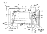
Z軸方向に平面的に見て長方形状の形状を有する第1上壁部431の内壁面437Aの第2上壁部432側の一方の角部付近には、第1部材446が配置されている。第1上壁部431の内壁面437Aの第2上壁部432側の他方の角部付近には、第2部材447が配置されている。X軸方向において、第2部材447が配置される側であって、第1側壁部411側の角部付近には、第3部材448が配置されている。すなわち、第1部材446および第2部材447は、第1上壁部431の長辺に沿って間隔をあけて、並べて配置されている。第2部材447および第3部材448は、第1上壁部431の短辺に沿って間隔をあけて、並べて配置されている。第1部材446および第2部材447は、Z軸方向に突出する第1突出部446A、第2突出部447Aと、Y軸方向に延びる第1爪部446B、第2爪部447Bとを含む。第1爪部446B、第2爪部447Bは、第1突出部446A、第2突出部447Aの第1上壁部431側とは反対側の端部から連なって配置される。第3部材448は、Z軸方向に突出する第3突出部448Aと、X軸方向に延びる第3爪部448Bと、を含む。第3爪部448Bは、第3突出部448Aの第1上壁部431とは反対側の端部から連なって配置される。
ケース40には、第1側壁部411、第2側壁部412、第4側壁部414、第1の領域421、段差部422Bおよび第1上壁部431によって取り囲まれた格納空間としての空間S1が形成されている。また、ケース40には、第2側壁部412、第3側壁部413、第4側壁部414、第2の領域422および第2上壁部432によって取り囲まれた空間S2が形成されている。第1上壁部431が取り外された場合には、Z軸方向に平面的に見て、第1側壁部411、第2側壁部412、第4側壁部414および第2上壁部432によって取り囲まれた開口部S3が形成される。
図2および図3を参照して、回路基板モジュール30は、第2の領域422上に配置されている。回路基板モジュール30は、第1基板31と、コネクタ接続部32と、を含む。第1基板31は、平板状の形状を有する。第1基板31は、第1突起部426および第2突起部427に対応する位置に厚み方向に貫通する貫通孔311,312が形成されている。貫通孔311,312に第1突起部426、第2突起部427が差し込まれて、第1基板31が第2の領域422に固定されている。
第1基板31は、第2上壁部432に対向する第1主面31Aと、第1主面31A側とは反対側の第2主面31Bと、を有する。図2および図3を参照して、コネクタ接続部32は、第2主面31B上に配置されている。コネクタ接続部32は、外部電源モジュール50および電池のコネクタが接続される接続部である。コネクタ接続部32は、第2の領域422の凹部422Aに対応する位置に配置されている。そのため、コネクタ接続部32は、空間S1から空間的につながった位置に配置されている。
入力部10は、センサからの入力を受ける。本実施の形態においては、入力部10は、3つの入力部からなる。入力部10は、第1基板31の第2主面31B上に配置され、回路基板モジュール30と電気的に接続されている。入力部10は、第4側壁部414の貫通孔414Aを介して外部空間からアクセス可能なように配置されている。
出力部20は、入力部10に入力されたセンサからの信号を無線信号に変換して出力する。出力部20は、第1基板31の第1主面31A上に配置され、回路基板モジュール30と電気的に接続されている。
特に図5~図8を参照して、外部電源モジュール50は、外部電源からの入力電圧を変換して出力電圧を出力するモジュールである。外部電源モジュール50は、第2基板51と、変換部52と、入力端子53と、出力端子54と、を含む。
第2基板51は、平板状の形状を有する。第2基板51は、厚み方向(Z軸方向)に平面的に見て、略長方形状の形状を有する。第2基板51は、一方側の第1主面51Aと、第1主面51Aとは厚み方向において反対側に位置する第2主面51Bと、を有する。第2基板51には、第3突起部441,442に対応する位置に厚み方向に貫通する貫通孔511,512が形成されている。第3突起部441,442が貫通孔511,512に差し込まれ、爪部443,444によって第2基板51は第1上壁部431に固定されている。その結果、第1主面51Aは、第1の領域421に対向するように配置される。第1主面51Aは、第1保持面421Aに対向するように配置される。第2主面51Bは、第1上壁部431の内壁面437Aに対向するように配置される。
入力端子53は、外部電源からの入力を受ける端子である。変換部52は、入力端子53に入力される入力電圧を所望の電圧に変換する。出力端子54は、変換部52によって変換された出力電圧を出力する端子である。変換部52、入力端子53および出力端子54は、第1主面51A上に配置されている。変換部52、入力端子53および出力端子54は、X軸方向に沿って配置されている。変換部52から見て、入力端子53が配置される側とは反対側に出力端子54が配置されている。図8を参照して、変換部52は、第1保持面421Aに対向するように配置されている。
入力端子53は、外部配線61のコネクタ62が接続可能な形状を有する。内部配線57の一方の端部にはコネクタ58Aが配置され、他方の端部にはコネクタ58Bが配置されている。コネクタ58Aは、出力端子54に接続可能な形状を有する。コネクタ58Bは、コネクタ接続部32(図2および図7参照)に接続可能な形状を有する。内部配線57のコネクタ58Bをコネクタ接続部32から着脱することで、外部電源モジュール50に内部配線57が接続された状態で、外部電源モジュール50を回路基板モジュール30から着脱することができる。
外部配線61のコネクタ62が入力端子53に接続されることで、外部電源と外部電源モジュール50とが電気的に接続される。コネクタ58Aが出力端子54に接続され、コネクタ58Bがコネクタ接続部32に接続されることで、外部電源モジュール50と、回路基板モジュール30とが電気的に接続される。なお、外部配線61は、第1側壁部411の切り欠き411Cに挿通されて、外部空間に引き出されている(特に図1参照)。
特に図9および図10を参照して、外部電源モジュール50を取り外すと、格納空間としての空間S1には、電池71,72を格納することができる。本実施の形態においては、円筒状の2つの電池が格納される。電池71,72のコネクタ73が、コネクタ接続部32に接続されることで、電池71,72と回路基板モジュール30とが電気的に接続される。電池71の外周面が第1保持面421Aに接触するようにして、電池71は保持される。電池72の外周面が第2保持面445に接触するようにして、電池72は保持される。すなわち、底壁部42の第1の領域421と、第1上壁部431とは、電池71,72を保持する保持部として機能する。
ここで、本実施の形態の無線端末装置1において、空間S1は、外部電源モジュール50を取り外すことにより、電池71,72を格納可能である。そして、回路基板モジュール30は、空間S1から空間的につながった位置に配置されたコネクタ接続部32を含む。このような構成とすることで、外部電源モジュール50のコネクタ58Bと、電池71,72のコネクタ73とを容易に付け替えることができる。そのため、外部電源を利用して、無線端末装置1を駆動することが可能であるとともに、電池71,72を取り付けて、電池71,72により無線端末装置1を駆動することが可能である。
上記実施の形態において、ケース40は、空間S1に配置され、電池を保持可能な円筒面状の第1保持面421Aおよび第2保持面445を有する。このような構成とすることで、空間S1において電池71,72を適切に保持し、電池71,72が移動することを規制することができる。
上記実施の形態において、ケース40から第1上壁部431が取り外された場合には、開口部S3が形成される。開口部S3から、空間S1に配置された外部電源モジュール50および電池71,72を取り出すことができる。
特に図6を参照して、外部配線61は、第1突出部446Aの周方向において半周を超えるように巻き付けられている。このような構成とすることで、外部配線61が引っ張られた際に、外部電源モジュール50と第1突出部446Aとの間において、外部配線61を引っ張る力が低減される。したがって、外部配線61が引っ張られたとしても、外部配線61のコネクタ62との接続部付近が受ける損傷を抑制することができる。
特に図6を参照して、第1突出部446Aの外周面と接触するように、外部電源モジュール50から延びる外部配線61が巻き付けられている。第2突出部447Aの外周面と接触するように、第1突出部446Aから延びる外部配線61が巻き付けられている。第2突出部447Aから延びる外部配線61は、第3部材448に保持され、外部空間に延びる。外部配線61が外部電源モジュール50から第1突出部446Aに向かう第1の方向L1に沿った第1の直線と、外部配線61が第1突出部446Aから第2突出部447Aに向かう第2の方向L2に沿った第2の直線と、を含む平面(X-Y平面)に垂直な方向(Z軸方向)に平面的に見て、第1の方向L1と、第2の方向L2とのなす角度が90度以下である。外部配線61が第3突出部448Aに向かう第3の方向L3に沿った第3の直線と、第2の直線と、を含む平面(X-Y平面)に垂直な方向(Z軸方向)に平面的に見て、第2の方向L2と、第3の方向L3とのなす角度が90度以下である。このような構成とすることで、外部配線61が引っ張られた際に、第1突出部446Aと第2突出部447Aとの間において、外部配線61を引っ張る力が低減される。さらに、外部電源モジュール50と第1突出部446Aとの間において、外部配線61を引っ張る力がさらに低減される。したがって、外部配線61が引っ張られたとしても、外部配線61のコネクタ62との接続部付近が受ける損傷をさらに抑制することができる。
(実施の形態2)
次に、本願の無線端末装置1の実施の形態2について説明する。実施の形態2の無線端末装置1は基本的には実施の形態1の無線端末装置1と同様の構造を有し、同様の効果を奏する。しかしながら、実施の形態2においては、電池を保持するための保持部の構成において、実施の形態1の場合とは異なっている。以下、実施の形態1の場合とは異なっている点について主に説明する。
次に、本願の無線端末装置1の実施の形態2について説明する。実施の形態2の無線端末装置1は基本的には実施の形態1の無線端末装置1と同様の構造を有し、同様の効果を奏する。しかしながら、実施の形態2においては、電池を保持するための保持部の構成において、実施の形態1の場合とは異なっている。以下、実施の形態1の場合とは異なっている点について主に説明する。
図11~図15を参照して、実施の形態2について説明する。図12は、図11の蓋部としての第1上壁部431を取り外した状態に対応する斜視図である。図13は、図11の蓋部としての第1上壁部431および外部電源モジュール50を取り外した状態に対応する斜視図である。図15は、図11における線分B-Bで切断した場合の断面図である。
ケース40は、側壁部41と、底壁部42と、上壁部43と、保持部43Aと、を含む。上壁部43は、第1上壁部431と、第2上壁部432と、を含む。第1上壁部431には、第2側壁部412側の端部であって、Y軸方向の中央に切り欠き481Aが形成されている。切り欠き481Aは、第1上壁部431をケース40に取り付けることで、貫通孔を構成する。切り欠き481Aは、外部配線61が挿通可能な形状を有する。
保持部43Aは、Z軸方向に平面的に見て、第1上壁部431に対応するように配置される。保持部43Aは、底壁部42、第2側壁部412、第3側壁部413、第4側壁部414および第1上壁部431に囲まれる格納空間S1内に配置される。保持部43Aは、接続部455により第2上壁部432に接続される。保持部43Aは、円筒面状に凹んだ第3保持面456を有している。第3保持面456は、円筒状の電池74(特に図16参照)を保持可能な形状を有する。保持部43Aには、Y軸方向に沿って突出する爪部453Bが形成されている。保持部43Aには、爪部453Bに沿ってX軸方向に延びる貫通孔453Aが形成されている。
回路基板モジュール30の入力部10は、第1側壁部411のX軸方向の中央から第2上壁部432に至る凹部411Aから露出するように配置されている。回路基板モジュール30のコネクタ接続部32は、接続部455に形成された貫通孔455Aから露出するように配置されている。
外部電源モジュール50は、第2基板51と、変換部52と、入力端子53と、出力端子54と、保持部材59と、を含む。保持部材59は、第2基板51を保持する部材である。保持部材59は、側壁部55と、底蓋部56と、を含む。側壁部55は、第1部分571と、第2部分572と、第3部分573と、第4部分574と、を含む。第1部分571~第4部分574は、板状の形状を有する。第1部分571と、第3部分573とは、Y軸方向に間隔をあけて平行に配置されている。第2部分572と、第4部分574と、X軸方向に間隔をあけて平行に配置されている。第2部分572のY軸方向の一方の端部には、第1部分571が接続されている。第2部分572のY軸方向の他方の端部には、第3部分573が接続されている。第4部分574のY軸方向の一方の端部には、第3部分573が接続されている。Z軸方向に平面的に見て、第2部分572は、第1部分571および第3部分573とのなす角が直角となるように配置されている。Z軸方向に平面的に見て、第4部分574は、第3部分573とのなす角が直角となるように配置されている。
第1部分571の底蓋部56とは反対側の端部であって、X軸方向の中央より第2部分572側には、厚み方向に貫通する第1切り欠き部571Aが形成されている。第1切り欠き部571Aは、内部配線57を挿通可能な形状を有する。第1部分571の底蓋部56とは反対側の端部であって、X軸方向の中央より第4部分574側には、厚み方向に貫通する第2切り欠き部571Bが形成されている。第2切り欠き部571Bは、外部配線61を挿通可能な形状を有する。
第1部分571の外壁面には、第1部材591と、第2部材592と、第3部材593と、第4部材594と、第5部材595と、第6部材596と、が配置されている。第2部材592および第4部材594は、X軸方向に沿って配置されている。第1部材591、第3部材593および第5部材595は、X軸方向に沿って配置されている。第6部材596は、第2部材592および第4部材594から見て、Z軸方向において、底蓋部56側とは反対側に配置されている。
第1部材591、第2部材592、第3部材593、第4部材594、第5部材595および第6部材596は、それぞれY軸方向に突出する第1突出部591A、第2突出部592A、第3突出部593A、第4突出部594A、第5突出部595A、第6突出部596Aと、Z軸方向に延在する第1爪部591B、第2爪部592B、第3爪部593B、第4爪部594B、第5爪部595B、第6爪部596Bと、を含む。第1爪部591B、第2爪部592B、第3爪部593B、第4爪部594B、第5爪部595B、第6爪部596Bは、第1突出部591A、第2突出部592A、第3突出部593A、第4突出部594A、第5突出部595A、第6突出部596Aの第1部分571側とは反対側の端部から連なって配置される。
外部配線61は、第1部材591、第2部材592および第3部材593に保持され、第4部材594に巻き付けられる。なお、外部配線61は、第4部材594の第4突出部594Aの周方向において半周を超えるように巻き付けられている。外部配線61は、第1上壁部431の切り欠き481Aに挿通されて、外部空間に引き出されている(特に図11参照)。内部配線57は、第6部材596に保持され、第5部材595の第5突出部595Aに巻き付けられている。
第2基板51の貫通孔511,512に底蓋部56に形成された柱状部561,562が差し込まれて、第2基板51は、側壁部55に囲まれた空間に配置される。第2基板51は、第1部分571、第2部分572、第3部分573および第4部分574に保持されている。変換部52、入力端子53および出力端子54は、第2基板51の第1主面51A上に配置されている。
特に図12および図15を参照して、外部電源モジュール50は、保持部43Aの第3保持面456に対向するように配置される。保持部材59における第4突起部573Aを保持部43Aの貫通孔453Aに差し込むようにして、外部電源モジュール50が配置される。その結果、第2基板51の第1主面51Aが、第3保持面456に対向するように配置される。このような構成とすることで、作業者が変換部52に触れて、変換部52に損傷を与えることを抑制することができる。変換部52は、円筒面状の第3保持面456の内側の空間を有効に利用して、格納される。
特に図12、図13および図16を参照して、外部電源モジュール50を取り外すと、格納空間としての空間S1には、電池74を格納することができる。電池74は、円筒状の形状を有する本体部741と、配線742A,742Bと、コネクタ73と、を含む。配線742A,742Bは、本体部741の電極に電気的に接続されている。配線742A,742Bの本体部741とは反対側の端部には、コネクタ73が接続されている。電池74のコネクタ73が、コネクタ接続部32に接続されることで、電池74と回路基板モジュール30とが電気的に接続される。本体部741の外周面741Aが第3保持面456に接触するようにして、電池74は保持される。すなわち、保持部43Aは、電池74を保持する保持部として機能する。
上記実施の形態2の無線端末装置1においても、回路基板モジュール30は、空間S1から空間的につながった位置に配置されたコネクタ接続部32を含む。このような構成とすることで、外部電源モジュール50のコネクタ58Bと、電池74のコネクタ73(特に図16参照)とを容易に付け替えることができる。したがって、上記実施の形態2の無線端末装置1によっても、実施の形態1と同様に、外部電源を利用して駆動させることができると共に、電池によっても駆動させることができる。
今回開示された実施の形態はすべての点で例示であって、どのような面からも制限的なものではないと理解されるべきである。本発明の範囲は上記した説明ではなく、請求の範囲によって規定され、請求の範囲と均等の意味および範囲内でのすべての変更が含まれることが意図される。
1 無線端末装置
10 入力部
20 出力部
30 回路基板モジュール
31 第1基板
31A,51A 第1主面
31B,51B 第2主面
32 コネクタ接続部
40 ケース
41 側壁部
42 底壁部
43 上壁部
43A 保持部
44,45,46 ねじ
50 外部電源モジュール
51 第2基板
52 変換部
53 入力端子
54 出力端子
55 側壁部
56 底蓋部
57 内部配線
58A,58B,62,73 コネクタ
59 保持部材
61 外部配線
71,72,74 電池
311,312,414A,453A,455A,511,512 貫通孔
411 第1側壁部
411A,422A,436,438A 凹部
411C 切り欠き
412 第2側壁部
413 第3側壁部
414 第4側壁部
421 第1の領域
421A 第1保持面
422 第2の領域
422B 段差部
423 第1の柱部
423A,424A,425A,433,434,435 ねじ穴
424 第2の柱部
425 第3の柱部
426 第1突起部
427 第2突起部
431 第1上壁部
432 第2上壁部
432B 外壁面
437A 内壁面
438,443,444,453B 爪部
441,442 第3突起部
445 第2保持面
446,591 第1部材
446A,591A 第1突出部
446B,591B 第1爪部
447,592 第2部材
447A,592A 第2突出部
447B,592B 第2爪部
448,593 第3部材
448A,593A 第3突出部
448B,593B 第3爪部
455 接続部
456 第3保持面
481A 切り欠き
561,562 柱状部
571 第1部分
571A 第1切り欠き部
571B 第2切り欠き部
572 第2部分
573 第3部分
573A 第4突起部
574 第4部分
594 第4部材
594A 第4突出部
594B 第4爪部
595 第5部材
595A 第5突出部
595B 第5爪部
596 第6部材
596A 第6突出部
596B 第6爪部
741 本体部
741A 外周面
742A,742B 配線
S1,S2 空間
S3 開口部
10 入力部
20 出力部
30 回路基板モジュール
31 第1基板
31A,51A 第1主面
31B,51B 第2主面
32 コネクタ接続部
40 ケース
41 側壁部
42 底壁部
43 上壁部
43A 保持部
44,45,46 ねじ
50 外部電源モジュール
51 第2基板
52 変換部
53 入力端子
54 出力端子
55 側壁部
56 底蓋部
57 内部配線
58A,58B,62,73 コネクタ
59 保持部材
61 外部配線
71,72,74 電池
311,312,414A,453A,455A,511,512 貫通孔
411 第1側壁部
411A,422A,436,438A 凹部
411C 切り欠き
412 第2側壁部
413 第3側壁部
414 第4側壁部
421 第1の領域
421A 第1保持面
422 第2の領域
422B 段差部
423 第1の柱部
423A,424A,425A,433,434,435 ねじ穴
424 第2の柱部
425 第3の柱部
426 第1突起部
427 第2突起部
431 第1上壁部
432 第2上壁部
432B 外壁面
437A 内壁面
438,443,444,453B 爪部
441,442 第3突起部
445 第2保持面
446,591 第1部材
446A,591A 第1突出部
446B,591B 第1爪部
447,592 第2部材
447A,592A 第2突出部
447B,592B 第2爪部
448,593 第3部材
448A,593A 第3突出部
448B,593B 第3爪部
455 接続部
456 第3保持面
481A 切り欠き
561,562 柱状部
571 第1部分
571A 第1切り欠き部
571B 第2切り欠き部
572 第2部分
573 第3部分
573A 第4突起部
574 第4部分
594 第4部材
594A 第4突出部
594B 第4爪部
595 第5部材
595A 第5突出部
595B 第5爪部
596 第6部材
596A 第6突出部
596B 第6爪部
741 本体部
741A 外周面
742A,742B 配線
S1,S2 空間
S3 開口部
Claims (8)
- センサからの入力を受ける入力部と、
前記入力部に入力された前記センサからの信号を無線信号に変換して出力する出力部と、
前記入力部および前記出力部と電気的に接続された回路基板モジュールと、
前記回路基板モジュールと着脱可能に接続されており、外部電源からの入力を受ける入力端子を含み、前記入力端子に入力される入力電圧を変換して出力電圧を出力する外部電源モジュールと、
前記外部電源モジュールを格納する格納空間が形成されており、前記入力部、前記出力部、前記回路基板モジュールおよび前記外部電源モジュールを収容するケースと、を備え、
前記格納空間は、前記外部電源モジュールを前記回路基板モジュールから取り外すことにより、電池を格納可能であり、
前記回路基板モジュールは、前記外部電源モジュールのコネクタ、および前記電池のコネクタのうちいずれか一方を選択的に接続可能であって、前記格納空間から空間的につながった位置に配置されたコネクタ接続部を含む、無線端末装置。 - 前記ケースは、前記格納空間に配置され、前記電池を保持可能な円筒面状の保持面を有する保持部を含む、請求項1に記載の無線端末装置。
- 前記ケースには、前記格納空間と外部空間とを繋ぎ、前記格納空間に配置される前記外部電源モジュールおよび前記電池を取り出し可能な形状を有する開口部が形成されており、
前記ケースは、前記開口部を閉塞および開放可能に配置される蓋部を含み、
前記外部電源モジュールは、
第1主面および前記第1主面とは厚み方向において反対側に位置する第2主面を有する基板と、
前記第1主面上に配置され、前記外部電源から前記入力端子に入力される入力電圧を変換して出力電圧を出力する変換部と、を含み、
前記外部電源モジュールは、前記第2主面が前記蓋部に対向するように前記格納空間に格納される、請求項1または請求項2に記載の無線端末装置。 - 前記ケースには、前記格納空間と外部空間とを繋ぎ、前記格納空間に配置される前記外部電源モジュールおよび前記電池を取り出し可能な形状を有する開口部が形成されており、
前記ケースは、
前記開口部を閉塞および開放可能に配置される蓋部と、
前記格納空間に配置され、前記電池を保持可能な円筒面状の保持面を有する保持部と、を含み、
前記外部電源モジュールは、
第1主面および前記第1主面とは厚み方向において反対側に位置する第2主面を有する基板と、
前記第1主面上に配置され、前記外部電源から前記入力端子に入力される前記入力電圧を変換して前記出力電圧を出力する変換部と、を含み、
前記基板の前記第1主面は、前記保持面と対向する、請求項1に記載の無線端末装置。 - 前記ケースには、前記入力端子と前記外部電源とを接続する外部配線が挿通可能な形状を有する貫通孔が形成されている、請求項1から請求項4のいずれか1項に記載の無線端末装置。
- 前記ケースの内部に配置され、第1の向きに突出する第1突出部を有する第1部材をさらに備え、
前記第1突出部の外周面と接触するように、前記入力端子と前記外部電源とを接続する外部配線が巻き付けられている、請求項1から請求項5のいずれか1項に記載の無線端末装置。 - 前記外部配線は、前記第1突出部の周方向において半周を超えるように巻き付けられている、請求項6に記載の無線端末装置。
- 前記ケースの内部に配置され、第2の向きに突出する第2突出部を有する第2部材をさらに備え、
前記第1突出部の外周面と接触するように、前記外部電源モジュールから延びる前記外部配線が巻き付けられており、
前記第2突出部の外周面と接触するように、前記第1突出部から延びる前記外部配線が巻き付けられており、
前記外部配線が前記外部電源モジュールから前記第1突出部に向かう第1の方向に沿った第1の直線と、前記外部配線が前記第1突出部から前記第2突出部に向かう第2の方向に沿った第2の直線と、を含む平面に垂直な方向に平面的に見て、前記第1の方向と、前記第2の方向とのなす角度が90度以下であり、
前記外部配線が前記第2突出部から前記第1突出部側とは異なる側に向かう第3の方向に沿った第3の直線と、前記第2の直線と、を含む平面に垂直な方向に平面的に見て、前記第2の方向と、前記第3の方向とのなす角度が90度以下である、請求項6または請求項7に記載の無線端末装置。
Priority Applications (4)
| Application Number | Priority Date | Filing Date | Title |
|---|---|---|---|
| PCT/JP2019/000498 WO2020144804A1 (ja) | 2019-01-10 | 2019-01-10 | 無線端末装置 |
| CN201980066054.9A CN112805924B (zh) | 2019-01-10 | 2019-01-10 | 无线终端装置 |
| US17/293,484 US11700702B2 (en) | 2019-01-10 | 2019-01-10 | Wireless terminal device |
| JP2019528148A JP6562195B1 (ja) | 2019-01-10 | 2019-01-10 | 無線端末装置 |
Applications Claiming Priority (1)
| Application Number | Priority Date | Filing Date | Title |
|---|---|---|---|
| PCT/JP2019/000498 WO2020144804A1 (ja) | 2019-01-10 | 2019-01-10 | 無線端末装置 |
Publications (1)
| Publication Number | Publication Date |
|---|---|
| WO2020144804A1 true WO2020144804A1 (ja) | 2020-07-16 |
Family
ID=67690473
Family Applications (1)
| Application Number | Title | Priority Date | Filing Date |
|---|---|---|---|
| PCT/JP2019/000498 Ceased WO2020144804A1 (ja) | 2019-01-10 | 2019-01-10 | 無線端末装置 |
Country Status (4)
| Country | Link |
|---|---|
| US (1) | US11700702B2 (ja) |
| JP (1) | JP6562195B1 (ja) |
| CN (1) | CN112805924B (ja) |
| WO (1) | WO2020144804A1 (ja) |
Families Citing this family (4)
| Publication number | Priority date | Publication date | Assignee | Title |
|---|---|---|---|---|
| US7621293B2 (en) | 2001-04-05 | 2009-11-24 | Fisher Controls International Llc | Versatile emergency shutdown device controller implementing a pneumatic test for a system instrument device |
| JP7547043B2 (ja) * | 2019-12-04 | 2024-09-09 | ナブテスコ株式会社 | 航空機用の電子機器 |
| CN113124594A (zh) * | 2019-12-31 | 2021-07-16 | 青岛海尔特种电冰柜有限公司 | 电控元件防护罩及冷柜 |
| USD973605S1 (en) * | 2021-06-16 | 2022-12-27 | Kinova Inc. | Robotic arm controller |
Citations (3)
| Publication number | Priority date | Publication date | Assignee | Title |
|---|---|---|---|---|
| JP2000306185A (ja) * | 1999-04-21 | 2000-11-02 | Osaka Gas Co Ltd | 非常信号発信装置 |
| JP2005339078A (ja) * | 2004-05-26 | 2005-12-08 | Hitachi Ltd | 電子装置 |
| JP2008304124A (ja) * | 2007-06-07 | 2008-12-18 | Toshiba Corp | 二酸化炭素濃度測定用センサーシステム |
Family Cites Families (10)
| Publication number | Priority date | Publication date | Assignee | Title |
|---|---|---|---|---|
| KR20020007585A (ko) * | 2000-07-18 | 2002-01-29 | 이순 | 고출력 송신을 요구하는 휴대용 무선 단말기를 위한 밧테리 운용 방식 및 제어 회로 |
| KR20050088866A (ko) * | 2004-03-03 | 2005-09-07 | (주)싸이버뱅크 | 무선통신 단말기에서의 일회용 밧데리를 이용한 전원공급장치 |
| JP2009158446A (ja) * | 2007-12-28 | 2009-07-16 | Brother Ind Ltd | 携帯端末用電池蓋および携帯端末用カバー |
| CN101651359B (zh) * | 2009-09-10 | 2011-07-27 | 惠州Tcl移动通信有限公司 | 一种移动终端供电单元及移动终端供电切换方法 |
| US8593828B2 (en) * | 2010-02-04 | 2013-11-26 | Corning Cable Systems Llc | Communications equipment housings, assemblies, and related alignment features and methods |
| US8460030B2 (en) * | 2011-06-21 | 2013-06-11 | Nai-Chien Chang | Connector with detachable module |
| TWM432226U (en) * | 2012-01-03 | 2012-06-21 | Wistron Corp | Electronic apparatus and fixing structure for power module thereof |
| JP6327065B2 (ja) | 2014-08-28 | 2018-05-23 | 新日鐵住金株式会社 | 振動検出装置及び振動検出方法 |
| CN105652651B (zh) * | 2016-03-28 | 2018-01-16 | 京东方科技集团股份有限公司 | 可穿戴物品 |
| US11567111B2 (en) * | 2018-11-10 | 2023-01-31 | Setra Systems, Inc. | Measurement device and method of its operation |
-
2019
- 2019-01-10 JP JP2019528148A patent/JP6562195B1/ja active Active
- 2019-01-10 CN CN201980066054.9A patent/CN112805924B/zh active Active
- 2019-01-10 WO PCT/JP2019/000498 patent/WO2020144804A1/ja not_active Ceased
- 2019-01-10 US US17/293,484 patent/US11700702B2/en active Active
Patent Citations (3)
| Publication number | Priority date | Publication date | Assignee | Title |
|---|---|---|---|---|
| JP2000306185A (ja) * | 1999-04-21 | 2000-11-02 | Osaka Gas Co Ltd | 非常信号発信装置 |
| JP2005339078A (ja) * | 2004-05-26 | 2005-12-08 | Hitachi Ltd | 電子装置 |
| JP2008304124A (ja) * | 2007-06-07 | 2008-12-18 | Toshiba Corp | 二酸化炭素濃度測定用センサーシステム |
Also Published As
| Publication number | Publication date |
|---|---|
| CN112805924B (zh) | 2022-03-29 |
| US11700702B2 (en) | 2023-07-11 |
| US20220022333A1 (en) | 2022-01-20 |
| JPWO2020144804A1 (ja) | 2021-02-18 |
| JP6562195B1 (ja) | 2019-08-21 |
| CN112805924A (zh) | 2021-05-14 |
Similar Documents
| Publication | Publication Date | Title |
|---|---|---|
| WO2020144804A1 (ja) | 無線端末装置 | |
| CN106099789B (zh) | 电接线箱以及线束 | |
| EP1901579A2 (en) | Microphone module and mounting structure adapted to portable electronic device | |
| JP6797123B2 (ja) | 電気回路装置 | |
| JP2011071342A (ja) | 基板保持装置 | |
| JP6897778B2 (ja) | 回路基板アセンブリ及びこれを備える電動オイルポンプ | |
| US9231352B2 (en) | Module, and connection structure of module and mating connector | |
| US8415051B2 (en) | Battery storage structure for acoustic equipment | |
| JP6148598B2 (ja) | コネクタ | |
| US11527848B2 (en) | Grommet and apparatus for aligning wire | |
| CN209857286U (zh) | 麦克风组件及空调 | |
| JP4754972B2 (ja) | ドアハンドル装置 | |
| JP2008177871A (ja) | モジュール機器用電気機器 | |
| JP5248943B2 (ja) | 電子装置の通信回路の接続構造 | |
| JP2005174635A (ja) | コネクタの結合構造 | |
| JP2005178474A (ja) | 油封入機器と制御ユニットの取付構造 | |
| JP6703161B1 (ja) | ワイヤレスイヤホンに用いる内部モジュール | |
| JP7198136B2 (ja) | センサ装置 | |
| JP6703163B1 (ja) | 金属ストリップを利用して成形された内部モジュール | |
| JP6989047B1 (ja) | バッテリケース及びこれを用いた蓄電池システム | |
| US20230345680A1 (en) | Power conversion device | |
| US20250211883A1 (en) | Connector maximising the available technical volume | |
| CN214899273U (zh) | 引线保持结构及电动致动器 | |
| US12142780B2 (en) | Equipment component fixation structure | |
| CN111698586B (zh) | 电子部件模块、其和壳体的组合及包括该组合的控制装置 |
Legal Events
| Date | Code | Title | Description |
|---|---|---|---|
| ENP | Entry into the national phase |
Ref document number: 2019528148 Country of ref document: JP Kind code of ref document: A |
|
| 121 | Ep: the epo has been informed by wipo that ep was designated in this application |
Ref document number: 19908365 Country of ref document: EP Kind code of ref document: A1 |
|
| NENP | Non-entry into the national phase |
Ref country code: DE |
|
| 122 | Ep: pct application non-entry in european phase |
Ref document number: 19908365 Country of ref document: EP Kind code of ref document: A1 |