WO2020138210A1 - 電子素子実装用基板、および電子装置 - Google Patents
電子素子実装用基板、および電子装置 Download PDFInfo
- Publication number
- WO2020138210A1 WO2020138210A1 PCT/JP2019/050928 JP2019050928W WO2020138210A1 WO 2020138210 A1 WO2020138210 A1 WO 2020138210A1 JP 2019050928 W JP2019050928 W JP 2019050928W WO 2020138210 A1 WO2020138210 A1 WO 2020138210A1
- Authority
- WO
- WIPO (PCT)
- Prior art keywords
- electronic element
- mounting substrate
- element mounting
- flow path
- electronic device
- Prior art date
- Legal status (The legal status is an assumption and is not a legal conclusion. Google has not performed a legal analysis and makes no representation as to the accuracy of the status listed.)
- Ceased
Links
Images






Classifications
-
- H—ELECTRICITY
- H10—SEMICONDUCTOR DEVICES; ELECTRIC SOLID-STATE DEVICES NOT OTHERWISE PROVIDED FOR
- H10W—GENERIC PACKAGES, INTERCONNECTIONS, CONNECTORS OR OTHER CONSTRUCTIONAL DETAILS OF DEVICES COVERED BY CLASS H10
- H10W76/00—Containers; Fillings or auxiliary members therefor; Seals
- H10W76/10—Containers or parts thereof
- H10W76/12—Containers or parts thereof characterised by their shape
-
- H—ELECTRICITY
- H10—SEMICONDUCTOR DEVICES; ELECTRIC SOLID-STATE DEVICES NOT OTHERWISE PROVIDED FOR
- H10W—GENERIC PACKAGES, INTERCONNECTIONS, CONNECTORS OR OTHER CONSTRUCTIONAL DETAILS OF DEVICES COVERED BY CLASS H10
- H10W76/00—Containers; Fillings or auxiliary members therefor; Seals
- H10W76/10—Containers or parts thereof
-
- H—ELECTRICITY
- H10—SEMICONDUCTOR DEVICES; ELECTRIC SOLID-STATE DEVICES NOT OTHERWISE PROVIDED FOR
- H10W—GENERIC PACKAGES, INTERCONNECTIONS, CONNECTORS OR OTHER CONSTRUCTIONAL DETAILS OF DEVICES COVERED BY CLASS H10
- H10W76/00—Containers; Fillings or auxiliary members therefor; Seals
- H10W76/10—Containers or parts thereof
- H10W76/12—Containers or parts thereof characterised by their shape
- H10W76/15—Containers comprising an insulating or insulated base
-
- H—ELECTRICITY
- H05—ELECTRIC TECHNIQUES NOT OTHERWISE PROVIDED FOR
- H05K—PRINTED CIRCUITS; CASINGS OR CONSTRUCTIONAL DETAILS OF ELECTRIC APPARATUS; MANUFACTURE OF ASSEMBLAGES OF ELECTRICAL COMPONENTS
- H05K1/00—Printed circuits
- H05K1/02—Details
-
- H—ELECTRICITY
- H10—SEMICONDUCTOR DEVICES; ELECTRIC SOLID-STATE DEVICES NOT OTHERWISE PROVIDED FOR
- H10W—GENERIC PACKAGES, INTERCONNECTIONS, CONNECTORS OR OTHER CONSTRUCTIONAL DETAILS OF DEVICES COVERED BY CLASS H10
- H10W70/00—Package substrates; Interposers; Redistribution layers [RDL]
- H10W70/60—Insulating or insulated package substrates; Interposers; Redistribution layers
-
- H—ELECTRICITY
- H10—SEMICONDUCTOR DEVICES; ELECTRIC SOLID-STATE DEVICES NOT OTHERWISE PROVIDED FOR
- H10W—GENERIC PACKAGES, INTERCONNECTIONS, CONNECTORS OR OTHER CONSTRUCTIONAL DETAILS OF DEVICES COVERED BY CLASS H10
- H10W76/00—Containers; Fillings or auxiliary members therefor; Seals
- H10W76/01—Manufacture or treatment
- H10W76/05—Providing fillings in containers, e.g. gas filling
-
- H—ELECTRICITY
- H10—SEMICONDUCTOR DEVICES; ELECTRIC SOLID-STATE DEVICES NOT OTHERWISE PROVIDED FOR
- H10H—INORGANIC LIGHT-EMITTING SEMICONDUCTOR DEVICES HAVING POTENTIAL BARRIERS
- H10H20/00—Individual inorganic light-emitting semiconductor devices having potential barriers, e.g. light-emitting diodes [LED]
- H10H20/80—Constructional details
- H10H20/85—Packages
- H10H20/8506—Containers
-
- H—ELECTRICITY
- H10—SEMICONDUCTOR DEVICES; ELECTRIC SOLID-STATE DEVICES NOT OTHERWISE PROVIDED FOR
- H10H—INORGANIC LIGHT-EMITTING SEMICONDUCTOR DEVICES HAVING POTENTIAL BARRIERS
- H10H20/00—Individual inorganic light-emitting semiconductor devices having potential barriers, e.g. light-emitting diodes [LED]
- H10H20/80—Constructional details
- H10H20/85—Packages
- H10H20/858—Means for heat extraction or cooling
- H10H20/8583—Means for heat extraction or cooling not being in contact with the bodies
-
- H—ELECTRICITY
- H10—SEMICONDUCTOR DEVICES; ELECTRIC SOLID-STATE DEVICES NOT OTHERWISE PROVIDED FOR
- H10W—GENERIC PACKAGES, INTERCONNECTIONS, CONNECTORS OR OTHER CONSTRUCTIONAL DETAILS OF DEVICES COVERED BY CLASS H10
- H10W70/00—Package substrates; Interposers; Redistribution layers [RDL]
- H10W70/60—Insulating or insulated package substrates; Interposers; Redistribution layers
- H10W70/67—Insulating or insulated package substrates; Interposers; Redistribution layers characterised by their insulating layers or insulating parts
- H10W70/68—Shapes or dispositions thereof
- H10W70/681—Shapes or dispositions thereof comprising holes not having chips therein, e.g. for outgassing, underfilling or bond wire passage
-
- H—ELECTRICITY
- H10—SEMICONDUCTOR DEVICES; ELECTRIC SOLID-STATE DEVICES NOT OTHERWISE PROVIDED FOR
- H10W—GENERIC PACKAGES, INTERCONNECTIONS, CONNECTORS OR OTHER CONSTRUCTIONAL DETAILS OF DEVICES COVERED BY CLASS H10
- H10W70/00—Package substrates; Interposers; Redistribution layers [RDL]
- H10W70/60—Insulating or insulated package substrates; Interposers; Redistribution layers
- H10W70/67—Insulating or insulated package substrates; Interposers; Redistribution layers characterised by their insulating layers or insulating parts
- H10W70/68—Shapes or dispositions thereof
- H10W70/682—Shapes or dispositions thereof comprising holes having chips therein
-
- H—ELECTRICITY
- H10—SEMICONDUCTOR DEVICES; ELECTRIC SOLID-STATE DEVICES NOT OTHERWISE PROVIDED FOR
- H10W—GENERIC PACKAGES, INTERCONNECTIONS, CONNECTORS OR OTHER CONSTRUCTIONAL DETAILS OF DEVICES COVERED BY CLASS H10
- H10W72/00—Interconnections or connectors in packages
- H10W72/50—Bond wires
- H10W72/541—Dispositions of bond wires
- H10W72/5445—Dispositions of bond wires being orthogonal to a side surface of the chip, e.g. parallel arrangements
-
- H—ELECTRICITY
- H10—SEMICONDUCTOR DEVICES; ELECTRIC SOLID-STATE DEVICES NOT OTHERWISE PROVIDED FOR
- H10W—GENERIC PACKAGES, INTERCONNECTIONS, CONNECTORS OR OTHER CONSTRUCTIONAL DETAILS OF DEVICES COVERED BY CLASS H10
- H10W76/00—Containers; Fillings or auxiliary members therefor; Seals
- H10W76/10—Containers or parts thereof
- H10W76/12—Containers or parts thereof characterised by their shape
- H10W76/167—Containers or parts thereof characterised by their shape the container walls comprising an aperture, e.g. for pressure control
-
- H—ELECTRICITY
- H10—SEMICONDUCTOR DEVICES; ELECTRIC SOLID-STATE DEVICES NOT OTHERWISE PROVIDED FOR
- H10W—GENERIC PACKAGES, INTERCONNECTIONS, CONNECTORS OR OTHER CONSTRUCTIONAL DETAILS OF DEVICES COVERED BY CLASS H10
- H10W76/00—Containers; Fillings or auxiliary members therefor; Seals
- H10W76/60—Seals
-
- H—ELECTRICITY
- H10—SEMICONDUCTOR DEVICES; ELECTRIC SOLID-STATE DEVICES NOT OTHERWISE PROVIDED FOR
- H10W—GENERIC PACKAGES, INTERCONNECTIONS, CONNECTORS OR OTHER CONSTRUCTIONAL DETAILS OF DEVICES COVERED BY CLASS H10
- H10W90/00—Package configurations
- H10W90/701—Package configurations characterised by the relative positions of pads or connectors relative to package parts
- H10W90/751—Package configurations characterised by the relative positions of pads or connectors relative to package parts of bond wires
- H10W90/754—Package configurations characterised by the relative positions of pads or connectors relative to package parts of bond wires between a chip and a stacked insulating package substrate, interposer or RDL
-
- H—ELECTRICITY
- H10—SEMICONDUCTOR DEVICES; ELECTRIC SOLID-STATE DEVICES NOT OTHERWISE PROVIDED FOR
- H10W—GENERIC PACKAGES, INTERCONNECTIONS, CONNECTORS OR OTHER CONSTRUCTIONAL DETAILS OF DEVICES COVERED BY CLASS H10
- H10W90/00—Package configurations
- H10W90/701—Package configurations characterised by the relative positions of pads or connectors relative to package parts
- H10W90/751—Package configurations characterised by the relative positions of pads or connectors relative to package parts of bond wires
- H10W90/755—Package configurations characterised by the relative positions of pads or connectors relative to package parts of bond wires between a chip and a laterally-adjacent insulating package substrate, interpose or RDL
Definitions
- the present disclosure relates to an electronic element mounting substrate on which electronic elements and the like are mounted, and an electronic device.
- a substrate for mounting an electronic element which includes a substrate having a concave portion including an insulating layer and a wiring layer. Further, such an electronic element mounting substrate is known to have a structure including a flow path communicating from the recess to the outside. (See JP 2007-128987 A).
- the electronic element mounting substrate is a flow path for replacing the air inside the electronic device with an appropriately selected substrate such as nitrogen after manufacturing the electronic device in which the electronic device is mounted in the recess and sealed with a lid or the like. Air may be injected/exhausted from. There was a concern that dust and the like would enter from the flow channel when the air in the concave portion was injected/exhausted using this flow channel.
- An electronic element mounting substrate includes a base body having a recessed portion including a mounting area in which an electronic element is mounted, a cutout portion located on an outer periphery in plan perspective, and an inner wall of the base body. And a flow path having an inner end and an outer end located on the outer periphery of the base body. The inner end of the flow path is open to the recess, and the outer end of the flow path is continuous with the notch.
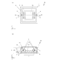
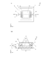
- FIG. 1A is a top view showing the appearance of an electronic element mounting substrate and an electronic device according to an embodiment of the present disclosure
- FIG. 1B is a vertical section corresponding to line X1-X1 of FIG. 1A. It is a side view.
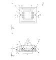
- FIG. 2A is a top view showing the appearance of the electronic element mounting substrate and the electronic device according to the first embodiment of the present disclosure
- FIG. 2B is taken along line X2-X2 of FIG. 2A. It is a corresponding longitudinal cross-sectional view.
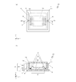
- FIG. 3A is a top view showing the appearance of an electronic device mounting substrate and an electronic device according to another aspect of the first embodiment of the present disclosure
- FIG. 3B is X3 of FIG. 3A.
- FIG. 6 is a vertical cross-sectional view corresponding to line X3.
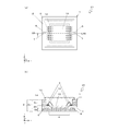
- FIG. 4A is a top view showing the external appearance of an electronic device mounting substrate and an electronic device according to another aspect of the first embodiment of the present disclosure, and FIG. 4B is X4 of FIG. 4A.
- FIG. 13 is a vertical sectional view corresponding to line X4.
- FIG. 5A is a top view showing the appearance of the electronic device mounting substrate and the electronic device according to the aspect of the first embodiment of the present disclosure, and FIG. 5B is X5-X5 of FIG. 5A. It is a longitudinal cross-sectional view corresponding to a line.
- FIG. 5A is a top view showing the external appearance of an electronic device mounting substrate and an electronic device according to another aspect of the first embodiment of the present disclosure
- FIG. 4B is X4 of FIG. 4A.
- FIG. 13 is a vertical sectional view corresponding to line X4.
- FIG. 5A is a top view showing the appearance of the electronic device mounting
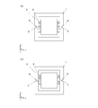
- FIG. 6A is a top view showing the external appearance of an electronic device mounting substrate and an electronic device according to an aspect of the second embodiment of the present disclosure
- FIG. 6B is X6-X6 of FIG. 6A. It is a longitudinal cross-sectional view corresponding to a line.
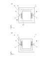
- FIG. 7A is a top view showing the appearance of the electronic device mounting substrate and the electronic device according to the third embodiment of the present disclosure
- FIG. 6B is taken along line X7-X7 of FIG. 6A. It is a corresponding cross-sectional view.
- FIG. 8A is a top view showing the external appearance of an electronic device mounting substrate and an electronic device according to another aspect of the third embodiment of the present disclosure
- FIG. 8B is X8 of FIG. 8A.
- FIG. 13 is a vertical sectional view corresponding to line X8.
- FIG. 9A is a top view showing the external appearance of the electronic device mounting substrate and the electronic device according to the aspect of the fourth embodiment of the present disclosure
- FIG. 9B is X9-X9 of FIG. 9A. It is a longitudinal cross-sectional view corresponding to a line.
- FIG. 10A is a top view showing the appearance of an electronic device mounting substrate and an electronic device according to another aspect of the fourth embodiment of the present disclosure
- FIG. 10B is X10 of FIG. 10A.
- FIG. 11 is a vertical sectional view corresponding to line X10.
- FIG. 11A is a top view showing the appearance of an electronic device mounting substrate and an electronic device according to another aspect of the fourth embodiment of the present disclosure, and FIG.
- FIG. 11B is X11 of FIG. 11A.
- FIG. 11 is a vertical sectional view corresponding to line X11.
- 12A and 12B are top views showing the outer appearance of the electronic element mounting substrate according to the aspect of the fifth embodiment of the present disclosure.
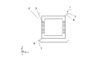
- FIG. 13 is a top view showing the appearance of an electronic element mounting substrate and an electronic device according to an aspect of the sixth embodiment of the present disclosure.
- FIG. 14 is a top view showing the external appearance of the electronic device according to the aspect of the seventh embodiment of the present disclosure.
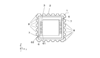
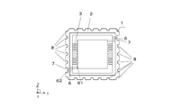
- 15A and 15B are top views showing an electronic element mounting substrate according to another aspect of the seventh embodiment of the present disclosure.
- FIG. 16 is a top view showing an electronic element mounting substrate according to another aspect of the seventh embodiment of the present disclosure.
- an electronic device has a configuration in which an electronic element is mounted on an electronic element mounting substrate.
- the electronic element mounting substrate and the electronic device may be either upward or downward, but for convenience, the orthogonal coordinate system xyz is defined and the positive side in the z direction is upward.
- the electronic element has, for example, an imaging element such as a CCD (Charge Coupled Device) type or a CMOS (Complementary Metal Oxide Semiconductor) type, a light emitting element such as an LED (Light Emitting Diode), and a sensor function such as pressure, atmospheric pressure, acceleration, and gyro.
- an imaging element such as a CCD (Charge Coupled Device) type or a CMOS (Complementary Metal Oxide Semiconductor) type
- a light emitting element such as an LED (Light Emitting Diode)
- a sensor function such as pressure, atmospheric pressure, acceleration, and gyro.
- FIGS. 2 to 5 An electronic device mounting board 1 according to the first embodiment of the present disclosure and an electronic device 21 including the same will be described with reference to FIGS. 2 to 5. In this embodiment, the electronic device 21 is shown in FIGS. 2 to 5.
- the electronic element mounting substrate 1 has a mounting area 4 on which an electronic element 10 is mounted, and a substrate 2a having a cutout portion 7 on the outer periphery in plan perspective.
- On the upper surface of the substrate 2a there is a frame body 2d that surrounds the mounting area 4.
- the frame body 2d has a flow path 6 having an inner end 61 located on the inner wall of the frame body 2d and an outer end 62 located on the outer periphery of the frame body 2d or the substrate 2a.
- the outer end 62 of the flow path 6 is continuous with the cutout portion 7.
- the electronic element mounting substrate 1 has a mounting area 4 on which an electronic element 10 is mounted, and a substrate 2a having a cutout portion 7 on the outer periphery in plan perspective. On the upper surface of the substrate 2a, there is a frame body 2d that surrounds the mounting area 4.
- the mounting region 4 is a region in which at least one or more electronic elements 10 are mounted, and may be, for example, the innermost periphery of an electrode pad 3 described later, a region in which a lid is mounted, or more, as appropriate. It is possible to set. Further, the component mounted in the mounting area 4 is not limited to the electronic element 10, and may be an electronic component, for example, and the number of the electronic element 10 and/or the electronic component is not specified.
- the substrate 2a has a cutout portion 7.
- one semicircular cutout 7 is provided on each of the left and right sides.
- the notch 7 may have a shape other than a semi-circle, and the place and the number thereof can be arbitrarily set.
- the size in the z direction may be only the substrate 2a, may penetrate the frame 2d, or may extend from the lower surface of the base 2 to the middle of the base 2.
- the inner end 61 of the channel 6 may be located on the bottom surface of the recess 20 of the substrate 2 and may be connected to the outside. In these cases as well, it is possible to achieve individual effects.
- the frame body 2d may be composed of only the first frame body 2b or the second frame body 2c, or may be composed of both the first frame body 2b and the second frame body 2c. Further, the number of frame bodies such as the third frame body and the fourth frame body may be increased.
- the base body 2 including the substrate 2a, the first frame body 2b, and the second frame body 2c is composed of a plurality of insulating layers.
- the base body 2 including the substrate 2a, the first frame body 2b, and the second frame body 2c is composed of a plurality of insulating layers.
- the structure may be one formed by one layer or the like.
- the material of the insulating layer forming the base 2 includes, for example, electrically insulating ceramics or resin.
- the recess 20 of the base 2 is in a state of being surrounded by the substrate 2a and the frame 2d.
- the mounting area 4 is provided on the upper surface of the base 2.
- the base 2 has a channel 6 having an inner end 61 located on the inner wall of the base 2 and an outer end 62 located on the outer periphery of the base 2.
- the outer end 62 of the flow path 6 is continuous with the cutout portion 7. Further, the inner end 61 of the flow path 6 is open to the recess 20.
- Examples of the electrically insulating ceramics used as the material of the insulating layer forming the base body 2 include, for example, an aluminum oxide sintered body, a mullite sintered body, a silicon carbide sintered body, an aluminum nitride sintered body, and silicon nitride. A quality sintered body or a glass ceramic sintered body is included.
- the resin used as the material of the insulating layer forming the substrate 2 includes, for example, thermoplastic resin, epoxy resin, polyimide resin, acrylic resin, phenol resin or fluorine resin. Examples of the fluorine-based resin include tetrafluoroethylene resin.
- the substrate 2 may be formed of seven insulating layers as shown in FIG. 2, or may be formed of six or less insulating layers or eight or more insulating layers. When the number of insulating layers is 6 or less, the electronic element mounting substrate 1 can be thinned. When the number of insulating layers is eight or more, the rigidity of the electronic element mounting substrate 1 can be increased.
- the electronic element mounting substrate 1 has, for example, a size of one side of the outermost periphery of 0.3 mm to 10 cm.
- the electronic element mounting substrate 1 may have a quadrangular shape in a plan view, it may have a square shape or a rectangular shape. Further, for example, the thickness of the electronic element mounting substrate 1 is 0.2 mm or more.
- the frame body 2d of the electronic element mounting substrate 1 has a flow path 6 having an inner end 61 located on the inner wall of the frame body 2d and an outer end 62 located on the outer periphery of the frame body 2d or the substrate 2a.
- the outer end 62 of the flow path 6 is continuous with the cutout portion 7.
- the flow path 6 may have a rectangular shape in a cross-sectional view taken along line XX or may have a rectangular shape in a plan view perspective. Particularly in the cross-sectional view, the rectangular shape shortens the distance between the outside of the base body 2 and the inside of the base body 2, and makes it easy to inject/exhaust air from the flow path.
- the electronic element mounting substrate 1 is manufactured by manufacturing an electronic device in which an electronic element is mounted in a recessed portion and sealed with a lid or the like, and then the air inside the electronic device is replaced with a properly selected substrate such as nitrogen. Air may be injected/exhausted from the passage. There is a concern that dust and the like may enter from the flow channel when the air in the recess is injected/exhausted using this flow channel.
- the opening of the flow path 6 needs to have a certain size for injecting/exhausting air.
- the opening may be clogged with dust in the step of producing the flow path 6 and/or the step of moving the electronic element mounting substrate 1.
- the opening used for moving the electronic element mounting substrate 1 may be crushed by the equipment used in contact with the periphery of the opening.
- the cutout portion 7 can have a role of protecting the end portion of the flow passage 6. This makes it possible to reduce dust clogging in the openings of the flow paths 6.
- the flow path 6 is located at the end of the cutout portion 7, it is possible to reduce the contact of the equipment used when the electronic element mounting substrate 1 is moved around the opening. Become. For these reasons, it is possible to secure the area of the opening at the outer end of the flow path 6, and it is possible to reduce problems when performing air injection/exhaust using the flow path 6.
- the flow path 6 of the electronic element mounting substrate 1 is located between the substrate 2a and the first frame 2b.
- the electronic element mounting substrate 1 is between the substrate 2a and the first frame 2b, and the flow path 6 penetrating outward from the inner wall of the first frame 2b. have.
- one end of the opening of the flow path 6 is located below the electrode pad 3 described later in the cross-sectional view taken along line X2-X2.
- the electrode pad 3 may be provided on the upper surface of the substrate 2a or the upper surface of the first frame 2b.
- the electrode pad 3 refers to a pad electrically connected to the electronic element 10, for example.
- an external circuit connecting electrode may be provided on the upper surface, side surface or lower surface of the base body 2 of the electronic element mounting substrate 1.
- the external circuit connecting electrode may electrically connect the base 2 and the external circuit board or the electronic device 21 and the external circuit board.
- electrodes formed between insulating layers, internal wiring conductors, and penetrating conductors for vertically connecting the internal wiring conductors are provided. May be These electrodes, internal wiring conductors or through conductors may be exposed on the surface of the base 2.
- the electrode pad 3 and/or the external circuit connecting electrode may be electrically connected to each other by this electrode, the internal wiring conductor or the penetrating conductor.
- the electrode pad 3, the electrode for external circuit connection, the internal wiring conductor and/or the through conductor are made of tungsten (W), molybdenum (Mo), manganese (Mn), palladium (when the substrate 2 is made of electrically insulating ceramics). Pd), silver (Ag), copper (Cu), or an alloy containing at least one metal material selected from these, and the like. Further, it may be made of only copper (Cu).
- the external circuit connecting electrode, the internal wiring conductor and/or the through conductor when a plurality of layers are made of resin, copper (Cu), gold (Au), aluminum (Al), nickel ( Ni), molybdenum (Mo), palladium (Pd), titanium (Ti), or an alloy containing at least one metal material selected from these is included.
- a plating layer may be further provided on the exposed surface of the electrode pad 3, the external circuit connecting electrode, the electrode, the internal wiring conductor and/or the through conductor.
- the exposed surface of the electrode for external circuit connection, the conductor layer, and the through conductor can be protected to reduce oxidation.
- the electrode pad 3 and the electronic element 10 can be satisfactorily electrically connected to each other via the connection conductor 13 such as a wire.
- the plating layer for example, a Ni plating layer having a thickness of 0.5 ⁇ m to 10 ⁇ m may be applied, or the Ni plating layer and a gold (Au) plating layer having a thickness of 0.5 ⁇ m to 3 ⁇ m may be applied in sequence. Good.
- the flow path 6 of the electronic element mounting substrate 1 is located above the electrode pad 3.
- the electrode pad 3 is located on the upper surface of the substrate 2a or the first frame 2b, and the flow path 6 penetrating outward from the inner wall of the second frame 2c. have.
- one end of the opening of the flow path 6 is located above the electrode pad 3 in a cross sectional view taken along line X4-X4.
- the electronic element mounting substrate 1 may have the electrode pads 3 located on the upper surface of the first frame portion 2b as in the example shown in FIGS. 3 and 4, or the upper surface of the substrate 2a as in the example shown in FIG. May be located at.
- the electronic element mounting substrate 1 has the upper surface of the first frame portion 2b on which the electrode pads 3 are located as in the example shown in FIGS.
- the position of the electrode pad 3 in the cross-sectional view can be set to the same height position. Therefore, the length of the wire 13 can be shortened. This makes it possible to improve the electrical characteristics. Furthermore, since the length of the wire 13 is short, it is possible to reduce the amount of bending of the wire 13 in the step of injecting/exhausting air using the flow path 6. Therefore, it is possible to reduce the contact of the wires 13 of the adjacent electrode pads 3 with each other, and it is possible to improve the effect of the present embodiment.
- one end of the opening of the flow path 6 is located below the electrode pad 3 in a cross-sectional view, so that dust entering from the flow path 6 is unlikely to adhere to the vicinity of the electrode pad 3. Therefore, even when the electronic device 21 is vibrated from the outside, it is possible to reduce dust from adhering between the electrode pads 3 and causing a short circuit between the electrode pads 3. Therefore, malfunction of the electronic device 21 can be reduced.
- the electronic element mounting substrate 1 has a second frame 2c located on the upper surface of the first frame 2b so as to surround the electrode pad 3 and the mounting region 4.
- the inner edge of the second frame body 2c is a plane from the upper surface rather than the inner edge of the first frame body 2b, as shown in FIG. It is shown to be located outside in the perspective view.
- the inner edge of the second frame body 2c overlaps with the inner edge of the first frame body 2b as seen in a plan view from above, as shown in FIG. It may be located, or the inner edge thereof may be located more inward than the inner edge of the first frame body 2b when seen in a plan view from above.
- the electronic element mounting substrate 1 has the electrode pads 3 located on the upper surface of the first frame body 2b and has the flow path 6 penetrating outward from the inner wall of the second frame body 2c. ing.
- one end of the opening of the flow path 6 is located above the electrode pad 3 in a sectional view.
- the flow path is only exhausted so that water vapor and the like do not collect inside the electronic device in the process of joining the lid etc. when creating the electronic device (air injection/exhaustion). May not be done intentionally).
- air injection/exhaustion since air is not intentionally discharged, if dust or the like enters from the flow channel when the flow channel is the same as or in the vicinity of the electrode, for example, the next process can be performed while keeping the dust in the vicinity of the electrode. I will welcome you. After that, when the electronic device is mounted on an external device and then vibration or the like is applied to the electronic device from the outside, there is a concern that dust located in the vicinity of the electrode may move to cause a short circuit between the electrodes to cause a malfunction.
- one end of the opening of the flow channel 6 is located above the electrode pad 3 in a cross-sectional view, so that dust entering from the flow channel 6 adheres to the vicinity of the electrode pad 3. It will be hard. Therefore, even when the electronic device 21 is vibrated from the outside, it is possible to reduce dust from adhering between the electrode pads 3 and causing a short circuit between the electrode pads 3. Therefore, malfunction of the electronic device 21 can be reduced.
- the electrode pad 3 of the electronic element mounting substrate 1 is located inside the second frame 2c, and the mounting region 4 is located inside the electrode pad 3.
- the electrode pad 3 of the electronic element mounting substrate 1 and the electronic element 10 mounted in the mounting region 4 do not overlap with each other when seen in a plan view, and the electrode pad 3 is located on the upper surface of the first frame body 2b. ing.
- the end portion of the flow path 6 can be located inside the end portion of the electrode pad 3 above the electrode pad 3 in plan view.
- the electronic element mounting substrate 1 has the electrode pads 3 positioned on the upper surface of the first frame portion 2a as in the example shown in FIG. 3, so that the upper surface of the electronic element 10 mounted on the mounting area 4 and the electrode pad 3 are mounted.
- the electronic element mounting substrate 1 is located on the upper surface of the substrate 2a as in the example shown in FIG. 5, the structure of the substrate 2 is facilitated, the yield is improved, and the height of the wire 13 is kept low. It becomes possible to reduce the height. Furthermore, since the height of the wire 13 can be suppressed to be low, it is possible to reduce the area of the portion where the flow path 6 and the wire 13 have approximately the same height in cross section. Therefore, it is possible to reduce the area that directly contacts the wire 13 during the air injection/exhaust, and it is possible to further improve the effect of the present embodiment.
- the second frame 2c of the electronic element mounting substrate 1 may have a plurality of layers, and the flow path 6 may be located above the first layer from the bottom of at least the plurality of layers. This makes it possible to increase the distance from the electrode pad 3 in a sectional view. Therefore, in the step of injecting/exhausting air using the flow path 6, it is possible to reduce the air directly hitting the wire 13 or reduce the area where the air hits the wire 13. Therefore, the effect of this embodiment can be further improved.
- the second frame 2c of the electronic element mounting substrate 1 has a plurality of layers, and the flow path 6 may have a thickness of at least one layer in a cross-sectional view. This allows smoother injection/drainage. Therefore, the air can be injected/exhausted without increasing the output, and the amount of bending of the wire 13 can be reduced. Further, it becomes possible to reduce the mixing of dust.
- the electronic device 21 includes the electronic element mounting substrate 1 and the electronic element 10 mounted on the upper surface of the electronic element mounting substrate 1.
- the electronic device 21 has an electronic element mounting substrate 1 and an electronic element 10 mounted on a mounting area 4 of a substrate 2 a of the electronic element mounting substrate 1.
- an image pickup device such as a CCD (Charge Coupled Device) type or a CMOS (Complementary Metal Oxide Semiconductor) type
- a light emitting device such as an LED (Light Emitting Diode)
- pressure atmospheric pressure, acceleration, a gyro, etc.
- the electronic element 10 may be arranged on the upper surface of the substrate 2a via an adhesive material.
- the adhesive material for example, silver epoxy or thermosetting resin is used.
- the electronic element 10 and the electronic element mounting substrate 1 may be electrically connected by a wire 13, for example.
- the electronic device 21 may have the lid 12 that covers the electronic element 10 and is joined to the upper surface of the electronic element mounting substrate 1.
- the lid body for example, when the electronic element 10 is an image pickup element such as a CMOS or CCD, or a light emitting element such as an LED, a highly transparent member such as a glass material is used. Further, for example, when the electronic element 10 is an integrated circuit or the like, the lid may be made of a metal material, a ceramic material, or an organic material.
- the lid 12 may be joined to the electronic element mounting substrate 1 via the lid connecting member 14.
- the material forming the lid connecting member 14 include a thermosetting resin, low melting point glass, or a brazing material made of a metal component.
- the flow path 6 may be filled with an end portion located outside with resin or the like. As a result, it is possible to reduce dust mixing from the flow path after the step of injecting/exhausting air or the step of joining the lid 12. At this time, it is also possible to apply a metal layer to the inner wall of the flow path 6 to perform sealing by using, for example, a brazing material.
- the flow path 6 may be opened even after the step of manufacturing the electronic device 21.
- the electronic device 21 is connected to an external device, and when the user actually uses the electronic device 21, it is possible to adjust the amount of water in the electronic device 21 due to, for example, fluctuations in atmospheric pressure or fluctuations in temperature.
- the electronic device 21 Since the electronic device 21 has the electronic element mounting substrate 1 as shown in FIG. 2, it is possible to reduce the occurrence of a short circuit due to the adjacent wires 13 coming into contact with each other in the step of injecting/exhausting air into the flow path 6. This makes it possible to reduce the yield of the electronic device 21. In addition, it is possible to reduce the possibility that dust entering from the flow path 6 is located between the plurality of electrode pads 3 and short-circuited, and malfunction of the electronic device 21 can be reduced.
- a ceramic green sheet that forms the base 2 (the substrate 2a, the first frame 2b, and the second frame 2c) is formed.
- the base 2 which is an aluminum oxide (Al 2 O 3 ) sintered body
- a suitable binder, solvent and plasticizer are added, and then a mixture of these is kneaded to form a slurry.
- a ceramic green sheet for obtaining a large number of pieces is obtained by a forming method such as a doctor blade method or a calendar roll method.
- the base 2 is made of resin
- a mold capable of being molded into a predetermined shape is used, and the base 2 is molded by transfer molding, injection molding, pressing with a mold or the like. Can be formed.
- the base 2 may be formed by impregnating a resin made of a glass fiber base material such as glass epoxy resin.
- the substrate 2 can be formed by impregnating a base material made of glass fiber with a precursor of an epoxy resin and thermally curing the epoxy resin precursor at a predetermined temperature.
- the green sheet described above is processed by a mold or the like.
- openings are formed in the first frame body 2b and the second frame body 2c.
- the notch or the like may be similarly formed at a predetermined position of the green sheet that becomes the base 2.
- a through hole which becomes the flow path 6 may be formed in the green sheet which becomes the first frame 2b or the second frame 2c by using a mold or a laser.
- the ceramic green sheets to be the insulating layers of the base 2 are laminated and pressed.
- the green sheets to be the respective insulating layers may be laminated to produce a ceramic green sheet laminated body to be the substrate 2 (electronic element mounting substrate 1).
- the notch or the like may be appropriately formed with a mold or the like.
- the ceramic green sheet or the ceramic green sheet laminate obtained in the above steps (1) to (3) is attached to the electrode pad 3, the external circuit connecting electrode, the internal wiring conductor, A metal paste is applied or filled in a portion to be an internal through conductor.
- This metal paste is prepared by adding an appropriate solvent and a binder to the metal powder made of the above-mentioned metal material and kneading the mixture to adjust the viscosity to an appropriate level.
- the metal paste may contain glass or ceramics in order to increase the bonding strength with the base body 2.
- the electrode pad 3, the external circuit connecting electrode, the internal wiring conductor and the through conductor can be produced by a sputtering method, a vapor deposition method or the like.
- the metal film may be provided on the surface and then plated.
- the ceramic green sheet laminate is fired at a temperature of about 1500° C. to 1800° C. to obtain a multi-cavity wiring board in which a plurality of bases 2 (electronic element mounting boards 1) are arranged.
- the above-mentioned metal paste is fired at the same time as the ceramic green sheet that becomes the base 2 (electronic element mounting substrate 1) and becomes the electrode pad 3, the external circuit connecting electrode, the internal wiring conductor and the through conductor. ..
- the multi-cavity wiring board obtained by firing is divided into a plurality of substrates 2 (electronic element mounting board 1).
- a dividing groove is formed in the step (5) in the multi-cavity wiring board along the outer edge of the substrate 2 (electronic element mounting substrate 1), and the dividing groove is broken along the dividing groove.
- the step (5) is not performed and the substrate 2 (electronic element mounting substrate 1) is cut along the outer edge of the substrate 2 by a slicing method or the like.
- plating may be applied to the electrode pads 3, external connection pads and exposed wiring conductors by electrolytic or electroless plating, respectively. Good.
- the electronic element 10 is mounted on the electronic element mounting substrate 1.
- the electronic element 10 is electrically connected to the electronic element mounting substrate 1 with a wire 13.
- an adhesive or the like may be provided on the electronic element 10 or the electronic element mounting substrate 1 to fix the electronic element mounting substrate 1 to the electronic element mounting substrate 1.
- the lid 12 may be joined by the lid joining member 14 after the electronic element 10 is mounted on the electronic element mounting substrate 1.
- appropriately selected air may be injected/exhausted into the electronic device 21 using the flow path 6.
- the electronic device 21 can be manufactured by manufacturing the electronic element mounting substrate 1 and mounting the electronic element 10 as in the steps (1) to (7) above. It should be noted that the order of steps (1) to (8) is not specified as long as it is a workable order. Further, it is possible to manufacture it by using a 3D printer or the like other than the steps described above.
- the notch 7 has a U shape or a U shape. Since the notch portion 7 is U-shaped or U-shaped, the area of the opening at the end portion on the outer side of the flow path 6 is further increased as compared with the semi-circular notch portion 7 as in the example shown in FIG. It becomes easy to secure. Therefore, it is possible to reduce problems when the air is injected/exhausted using the channel 6. Further, in the example shown in FIG. 6, the notch 7 can be made sufficiently larger than the flow path 6. As a result, the position of the flow path 6 can be accommodated in the cutout portion 7 even if the position shift occurs. Therefore, the positional deviation between the flow path 6 and the cutout portion 7 can reduce problems when the air is injected/exhausted in the recess 20. The same effect can be obtained as in the case where no displacement occurs in this way.
- the manufacturing method of the electronic element mounting substrate 1 and the electronic device 21 of the present embodiment is basically similar to the manufacturing method described in the first embodiment.
- the method for manufacturing the electronic element mounting substrate 1 of the present embodiment can be manufactured by changing the place where the portion to be the cutout portion 7 is formed in the step described in the first embodiment.
- FIGS. 7 and 8 An electronic element mounting substrate 1 according to a third embodiment of the present disclosure and an electronic device 21 including the same will be described with reference to FIGS. 7 and 8.
- the difference from the first embodiment is that the size of the cutout portion 7 of the substrate 2a in the Z direction is different in a longitudinal sectional view.
- the size of the cutout portion 7 in the Z direction is small and the cutout portion 7 is arranged only in the lower surface direction.
- the electronic element mounting board 1 and the electronic device 21 including the electronic element mounting board 1 have a shape without the cutout portion 7 in plan view. Therefore, it is possible to reduce the possibility that the dust falling from the upper direction of the electronic element mounting substrate 1 and the electronic device 21 including the electronic element mounting substrate 1 will be caught.
- the electronic device mounting substrate 1 and the electronic device 21 including the electronic device mounting substrate 1 have a rectangular outer shape in a top view without the cutout portion 7. In other words, there is no cutout 7 in the uppermost layer. As a result, it is possible to reduce the concentration of damage during handling, etc., in the vicinity of the cutout portion 7 and to reduce defects in the electronic element mounting substrate 1.
- the positional relationship between the flow path 6 and the cutout portion 7 is different between the example shown in FIG. 7 and the example shown in FIG.
- the cutout portion 7 is formed up to the upper side of the flow channel 6 in the cross sectional view, but in the example shown in FIG. 8, the cutout portion 7 is formed up to the same position in the cross sectional view as the flow channel 6.
- the electronic element mounting substrate 1 which is the upper portion of the cutout portion 7 is deformed and bent downward.
- the flow path 6 can be secured.
- the opening of the flow channel 6 is provided with a tool such as a nozzle in order to inject/exhaust air.
- a tool such as a nozzle
- the nozzle and the flow path 6 can be easily aligned, and the possibility of taking in dust when injecting air can be reduced. At this time, the effect of the present disclosure is more exerted if the shapes of the plurality of flow paths 6 are the same.
- the manufacturing method of the electronic element mounting substrate 1 and the electronic device 21 of the present embodiment is basically similar to the manufacturing method described in the first embodiment.
- the electronic element mounting substrate 1 can be manufactured by changing a portion of the cutout portion 7 in the Z direction in the step described in the first embodiment. it can.
- FIG. 11 shows a top view of the electronic element mounting substrate 1.
- the difference between the example shown in FIGS. 9 and 10 and the first embodiment is that the flow path 6 extends over two layers.
- the flow path 6 extends over two layers, and has a shape that is bent up and down in a longitudinal sectional view.
- the dust can be trapped at the bent portion of the flow path 6, and the inner end of the flow path 6 or the electronic device 21. It is possible to reduce the movement of dust to the inside of the. Therefore, it is possible to reduce the adhesion of dust to the electrode pads 3 or to the plurality of electrode pads 3 so as to short-circuit them.
- the example shown in FIG. 9 and the example shown in FIG. 10 differ in the bending direction of the flow path 6.
- the position of the flow path 6 of the first frame 2b is higher than the position of the flow path 6 in a cross-sectional view. Since the position of the flow path 6 of the first frame body 2b is high in cross section, it becomes possible to reduce the entrainment of dust. Therefore, since the dust is less likely to be caught in the recess 20, it is possible to reduce the adhesion of the dust to the electrode pads 3 or the plurality of electrode pads 3 so as to short-circuit them. Therefore, the effect of the present disclosure can be further improved.
- the position of the flow path 6 of the first frame body 2b is low in a sectional view.
- the dust trapped in the recess 20 can be easily discharged.
- the dust to the concave portion 20 it is possible to reduce the adhesion of the dust to the electrode pads 3 or the plurality of electrode pads 3 so as to short-circuit between the electrode pads 3. Therefore, the effect of the present disclosure can be further improved.
- the flow path 6 is only exhausted so that water vapor and the like are not accumulated inside the electronic device 21 in the step of joining the lid 12 etc. when the electronic device 21 is created. In other words, the air may not be intentionally injected or discharged.
- the flow path 6 is spread over two layers, but it may be spread over three layers or more, and the same effect as described above can be obtained.
- the flow path 6 has a bent shape in a plan view perspective.
- the difference between the example shown in FIG. 11 and FIG. 2 of the first embodiment is that the flow path 6 is refracted on the same plane.
- the dust can be trapped at the bent portion of the flow path 6, and the inner end of the flow path 6 or the electronic device 21. It is possible to reduce the movement of dust to the inside of the. Therefore, it is possible to reduce the adhesion of dust to the electrode pads 3 or to the plurality of electrode pads 3 so as to short-circuit them.
- each bent portion of the flow path 6 has a curved surface (arc).
- arc curved surface
- the upper and lower refracting portions and the bent portions on the same plane as in the example shown in FIG. 11 are simultaneously mounted on the electronic element mounting substrate 1, and an electronic device including the same. It is also possible to provide 21. In this case, it is possible to further reduce the dust in the concave portion 20, and it is possible to reduce the dust from adhering to the electrode pads 3 or short-circuiting between the plurality of electrode pads 3. Becomes
- the manufacturing method of the electronic element mounting substrate 1 and the electronic device 21 of the present embodiment is basically similar to the manufacturing method described in the first embodiment.
- the method for manufacturing the electronic element mounting substrate 1 of the present embodiment can be manufactured by changing the place where the portion to be the flow path 6 is formed in the step described in the first embodiment.
- FIG. 12 shows a top view of the electronic element mounting substrate 1.
- the difference between the example shown in FIG. 12A and FIG. 2 of the first embodiment is the shape of the flow path 6.
- the width of the channel 6 differs depending on the location of the channel 6.
- the plurality of flow paths 6 are larger in the end portion on the outer side than the end portion on the inner wall side of the first frame body 2b or the second frame body 2c in plan view. With such a configuration, it becomes difficult for dust to be mixed in from the external end of the flow path 6. Therefore, it is possible to reduce the possibility that dust entering from the flow path 6 is located between the plurality of electrode pads 3 and short-circuited. Further, when the flow path 6 is located between the first frame 2b and the substrate 2a, the flow path 6 may have a linear portion near the inner wall of the first frame 2b. As a result, it is possible to further reduce the mixing of dust, and it is possible to improve the effect of reducing the dust entering from the flow path 6 and being located between the plurality of electrode pads 3 and causing a short circuit.
- the plurality of flow paths 6 are smaller on the outer side end than on the inner wall side end of the first frame 2b in plan view.
- the air injected using the flow channel 6 can be diffused in a wide range, and the momentum of the air can be reduced around the inner end of the flow channel 6. Therefore, the amount of bending of the wire 13 can be reduced. Therefore, it is possible to reduce the occurrence of short circuit due to the contact of the wire 13.
- the flow path 6 When the flow path 6 is located between the first frame 2b and the substrate 2a, the flow path 6 may have a straight line portion near the inner wall of the first frame 2b. This makes it possible to diffuse the air injected using the flow channel 6 in a wide range, reduce the momentum of the air around the inner end portion of the flow channel 6, and further, from the electrode pad 3 to the flow channel 6. It is possible to separate the ends of. Therefore, it is possible to reduce the amount of bending of the wire 13, and it is possible to reduce the occurrence of short-circuiting of dust entering the flow path 6 between the plurality of electrode pads 3.
- the manufacturing method of the electronic element mounting substrate 1 and the electronic device 21 of the present embodiment is basically similar to the manufacturing method described in the first embodiment.
- the method for manufacturing the electronic element mounting substrate 1 of the present embodiment can be manufactured by changing the place where the portion to be the flow path 6 is formed in the step described in the first embodiment.
- the notch 7 is located at a corner of the base body 2 and is located at a position where the electrode pad 3 and the flow path 6 do not overlap with each other in plan view. That is the point.
- impact or pressure may be applied to the corners. It has been feared that the impact or stress applied to the corners may damage the substrate and cause defects such as chipping.
- the notch 7 is located at the corner of the base 2, it is possible to reduce the impact and stress applied to the corner, and reduce the dust generated by the impact and stress. It becomes possible.
- the electrode pad 3 and the flow path 6 are arranged at a position where they do not overlap with each other, it is possible to reduce occurrence of short circuit due to contact between the adjacent wires 13 in the step of injecting/exhausting air into the flow path 6. Moreover, it is possible to reduce the possibility that the dust entering from the flow path 6 is located between the plurality of electrode pads 3 and short-circuited. Therefore, it is possible to reduce the malfunction of the electronic device 21 while improving the yield of the electronic element mounting substrate 1. In addition, if the electrode pad 3 is not located near one end of the flow path 6 (on the virtual perpendicular line) as in the example shown in FIG. 13, even if dust enters from the flow path 6, it will flow.
- the effect of the present disclosure can be further improved. Further, the structure in which the electrode pad 3 is not located near one end of the flow path 6 (on the virtual perpendicular line) makes it possible to reduce the air hitting the electrode pad 3 at the time of injecting/exhausting air. ..
- the manufacturing method of the electronic element mounting substrate 1 and the electronic device 21 of the present embodiment is basically similar to the manufacturing method described in the first embodiment.
- the electronic element mounting substrate 1 is manufactured by changing the locations where the flow path 6 and the cutout portion 7 are formed in the steps described in the first embodiment. You can
- FIG. 11 shows a top view of the electronic element mounting substrate 1.
- the electronic device mounting board 1 according to the present embodiment is different from the electronic device mounting board 1 according to the first embodiment in that the base body 2 has a large number of groove portions 8 on the outer periphery.
- the groove 8 may have a semi-circular shape or a semi-elliptical shape.
- the channel 6 is provided in the groove portion 8 on the outer periphery of the base body 2
- the groove portion 8 on the outer periphery of the base body 2 is used as an external terminal to connect/fix to an external circuit with a conductive connecting material such as solder
- the flow channel 6 is simultaneously formed. Can be sealed with a conductive bonding agent.
- FIG. 15A has a groove portion 8 on the outer circumference, and the cutout portion 7 is larger than the groove portion 8 in a plan view or a plane perspective view. Since the cutout portion 7 is larger than the groove portion 8, the cutout portion 7 can be easily distinguished from the cutout portion 7 in which the flow path is installed. Further, it becomes easy to align the air when injecting/exhausting the air in the recess 20. The sizes may be compared in a plane view or a plane perspective view. Further, a plurality of groove portions 8 may be located.
- FIG. 15B has a groove portion 8 on the outer circumference, and the cutout portion 7 is smaller than the groove portion 8 in a plan view or a plane perspective view. Since the cutout 7 is smaller than the groove 8, the cutout 7 can be easily distinguished from the cutout 7 in which the flow path 6 is installed. Further, since the size of the cutout portion 7 is small, it is easy for the conductive bonding agent to crawl in the direction of the upper surface of the substrate 2. Therefore, when the groove 8 on the outer periphery of the substrate 2 is used as an external terminal and is connected/fixed to an external circuit with a conductive connecting material such as solder, the flow path 6 can be simultaneously sealed with a conductive bonding agent. Further, a plurality of groove portions 8 may be located.
- FIG. 16 has a groove portion 8 on the outer circumference, and the cutout portion 7 has a shape different from that of the groove portion 8. Since the notch 7 has a shape different from that of the other grooves 8, it is easy to distinguish them. Further, it becomes easier to determine the directionality as compared with the difference in size, and the process load can be reduced. Further, a plurality of groove portions 8 may be located.
- the present disclosure is not limited to the example of the above embodiment, and various modifications such as numerical values are possible.
- the shape of the electrode pad 3 is rectangular in a top view, but may be circular or other polygonal shape.
- the arrangement, number, shape, mounting method of electronic elements, etc. of the electrode pads 3 in the present embodiment are not specified.
- various combinations of the characteristic portions in this embodiment are not limited to the examples of the above-described embodiment. Also, a combination of the respective embodiments is possible.
Landscapes
- Engineering & Computer Science (AREA)
- Microelectronics & Electronic Packaging (AREA)
- Structure Of Printed Boards (AREA)
- Solid State Image Pick-Up Elements (AREA)
- Structures For Mounting Electric Components On Printed Circuit Boards (AREA)
- Led Device Packages (AREA)
Abstract
本開示の電子素子実装用基板は、電子素子が実装される実装領域を含む凹部と、平面透視における外周に位置した切欠き部と、を有する基体と、基体の内壁に位置した内端と、基体の外周に位置した外端とを有する流路と、を備えている。流路の内端は、凹部に開口しており、流路の外端は、切欠き部と連続している。
Description
本開示は、電子素子等が実装される電子素子実装用基板、および電子装置に関するものである。
絶縁層と配線層を含み、凹部を有する基板を備えた電子素子実装用基板が知られている。また、このような電子素子実装用基板は凹部から外部へ連通する流路を含む構造が知られている。(特開2007-128987号公報参照)。
電子素子実装用基板は、その凹部に電子素子が実装され蓋体などで封止された電子装置を作製した後、電子装置内部の空気を例えば窒素等の適宜選択した基体に入れ替えるために流路からエアーの注入/排出を行う場合がある。この流路を用いて前記凹部のエアーの注入/排出する際に、流路からダスト等が入る懸念があった。
また、電子装置を作成時において蓋体などを接合する工程において電子装置内部に水蒸気等がたまらないように排出だけを行う(エアーの注入排出を意図的に行わない)場合もある。この工程において、エアーを意図的に排出しないため、例えば流路が電極と同一またはその近傍にあるとダスト等が流路から入った場合において、ダストが電極近傍に位置したまま、次の工程を迎えてしまう。その後、電子装置を外部機器に搭載した後、電子装置に外部から振動などが加わった場合、その電極近傍に位置したダストが移動し電極間をショートさせ動作不良を起こすことが懸念されていた。
本開示の1つの態様に係る電子素子実装用基板は、電子素子が実装される実装領域を含む凹部と、平面透視における外周に位置した切欠き部と、を有する基体と、基体の内壁に位置した内端と、基体の外周に位置した外端とを有する流路と、を備えている。流路の内端は、凹部に開口しており、流路の外端は、切欠き部と連続している。
<電子素子実装用基板および電子装置の構成>
以下、本開示のいくつかの例示的な実施形態について図面を参照して説明する。なお、以下の説明では、電子素子実装用基板に電子素子が実装された構成を電子装置とする。電子素子実装用基板、および電子装置は、いずれの方向が上方若しくは下方とされてもよいが、便宜的に、直交座標系xyzを定義するとともに、z方向の正側を上方とする。電子素子は、例えばCCD(Charge Coupled Device)型またはCMOS(Complementary Metal Oxide Semiconductor)型等の撮像素子、LED(Light Emitting Diode)等の発光素子、圧力、気圧、加速度、ジャイロ等のセンサー機能を有する素子、または集積回路等のことを指す。
以下、本開示のいくつかの例示的な実施形態について図面を参照して説明する。なお、以下の説明では、電子素子実装用基板に電子素子が実装された構成を電子装置とする。電子素子実装用基板、および電子装置は、いずれの方向が上方若しくは下方とされてもよいが、便宜的に、直交座標系xyzを定義するとともに、z方向の正側を上方とする。電子素子は、例えばCCD(Charge Coupled Device)型またはCMOS(Complementary Metal Oxide Semiconductor)型等の撮像素子、LED(Light Emitting Diode)等の発光素子、圧力、気圧、加速度、ジャイロ等のセンサー機能を有する素子、または集積回路等のことを指す。
(第1の実施形態)
図2~図5を参照して本開示の第1の実施形態に係る電子素子実装用基板1、並びにそれを備えた電子装置21について説明する。なお、本実施形態では図2~図5では電子装置21を示している。
図2~図5を参照して本開示の第1の実施形態に係る電子素子実装用基板1、並びにそれを備えた電子装置21について説明する。なお、本実施形態では図2~図5では電子装置21を示している。
電子素子実装用基板1は、上面に電子素子10が実装される実装領域4を有し、平面透視における外周に切欠き部7を有する基板2aを有する。基板2aの上面には、実装領域4を囲んで位置した枠体2dがある。枠体2dは、枠体2dの内壁に位置した内端61と、枠体2dまたは基板2aの外周に位置した外端62を有する流路6を有している。この流路6の外端62は、切欠き部7と連続している。
電子素子実装用基板1は、上面に電子素子10が実装される実装領域4を有し、平面透視における外周に切欠き部7を有する基板2aを有する。基板2aの上面には、実装領域4を囲んで位置した枠体2dがある。
ここで、実装領域4とは少なくとも1つ以上の電子素子10が実装される領域であり、例えば後述する電極パッド3の最外周の内側、蓋体が実装される領域、またはそれ以上等、適宜定めることが可能である。また、実装領域4に実装される部品は電子素子10に限らず、例えば電子部品であってもよく、電子素子10または/および電子部品の個数は指定されない。
基板2aは、切欠き部7を有する。図2では、半円形の切欠き部7を左右の2辺に各1個有している。後述するが切欠き部7は、形状は半円形以外でも良く、場所や数は任意に設けることができる。z方向の大きさも基板2aだけでもよいし、枠体2dを貫通して存在してもよく、基体2の下面から基体2の途中まで存在していてもよい。また、流路6は、基体2の凹部20の底面に内端61が位置しており、外部に繋がっていてもよい。これらの場合またでも個々の効果を奏でることが可能となる。
枠体2dは、第1枠体2bもしくは、第2枠体2cのみで構成されていてもよいし、第1枠体2bと第2枠体2cの両方で構成されていてもよい。さらに、第3枠体、第4枠体等更に枠体が増加しても構わない。
以下、基板2a、第1枠体2bおよび第2枠体2cを合わせたものを基体2と称する。図2に示す例では、基板2a、第1枠体2bおよび第2枠体2cからなる基体2は複数の絶縁層で構成されているが、例えばモールドで形成された構成、金型等の押圧で形成された構成またはその他、1層のみの構成等であってもよい。基体2を構成する絶縁層の材料は例えば、電気絶縁性セラミックスまたは樹脂が含まれる。図1に示すように、基体2の凹部20は、基板2aおよび枠体2dで囲まれた状態のことである。このとき、基体2の上面には、実装領域4がある。基体2は、基体2の内壁に位置した内端61と、基体2の外周に位置した外端62を有する流路6を有している。この流路6の外端62は、切欠き部7と連続している。また、流路6の内端61は、凹部20に開口している。
基体2を形成する絶縁層の材料として使用される電気絶縁性セラミックスとしては例えば、酸化アルミニウム質焼結体、ムライト質焼結体、炭化珪素質焼結体、窒化アルミニウム質焼結体、窒化珪素質焼結体またはガラスセラミック焼結体等が含まれる。基板2を形成する絶縁層の材料として使用される樹脂としては例えば、熱可塑性の樹脂、エポキシ樹脂、ポリイミド樹脂、アクリル樹脂、フェノール樹脂またはフッ素系樹脂等が含まれる。フッ素系樹脂としては例えば、四フッ化エチレン樹脂が含まれる。
基体2は、図2に示すように7層の絶縁層から形成されていてもよいし、6層以下または8層以上の絶縁層から形成されていてもよい。絶縁層が6層以下の場合には、電子素子実装用基板1の薄型化を図ることができる。また、絶縁層が8層以上の場合には、電子素子実装用基板1の剛性を高めることができる。
電子素子実装用基板1は例えば、最外周の1辺の大きさは0.3mm~10cmである。平面視において電子素子実装用基板1が四角形状あるとき、正方形であってもよいし長方形であってもよい。また例えば、電子素子実装用基板1の厚みは0.2mm以上である。
電子素子実装用基板1の枠体2dは、枠体2dの内壁に位置した内端61と、枠体2dまたは基板2aの外周に位置した外端62を有する流路6を有している。この流路6の外端62は、切欠き部7と連続している。流路6は、X-X線での断面視において、矩形状であってもよいし、平面透視において、矩形状であってもよい。特に断面視において、矩形状であることによって、基体2の外部と基体2の内部との距離が短くなり、流路からエアーの注入/排出がしやすくなる。
電子素子実装用基板1は、その凹部に電子素子が実装され蓋体などで封止された電子装置を作製した後、電子装置内部の空気を例えば窒素等の適宜選択した基体に入れ替えるために流路からエアーの注入/排出を行う場合がある。この流路を用いて凹部のエアーの注入/排出する際に、流路からダスト等が入る懸念があった。
また、流路6の開口部はエアーを注入/排出するために一定の大きさが必要である。しかしながら、流路6を作製する工程または/および電子素子実装用基板1を移動させる工程等においてその開口にダストが詰まる懸念があった。また、電子素子実装用基板1の移動の際に使用される機具が開口部周辺に接することにより開口部がつぶされる懸念があった。
これに対し、流路6の端部が切欠き部7に位置していることで、切欠き部7部に流路6の端部を保護する役割を持たせることが可能となる。これにより、流路6の開口にダストが詰まることを低減させることが可能となる。また、流路6が切欠き部7の端部に位置していることで、電子素子実装用基板1の移動の際に使用される機具が開口部周辺に接することを低減させることが可能となる。これらのことから流路6の外側の端部の開口の面積を確保することが可能となり、流路6を用いてエアーの注入/排出を行う際の不具合を低減させることが可能となる。
図2に示す例では、電子素子実装用基板1の流路6は、基板2aと第1枠体2bとの間に位置している。
電子素子実装用基板は、その凹部に電子素子が実装され蓋体などで封止された電子装置を作製した後、電子装置内部の空気を例えば窒素等の適宜選択した基体に入れ替えるために流路からエアーの注入/排出を行う場合がある。近年、電子素子の端子は狭ピッチ化が進んでおり、電子素子と電子素子実装用基板とを電気的に接合するワイヤの径も小さくなっている。そのため、電子装置の流路を用いてエアーの注入/排出をする工程においてエアーの勢いでワイヤが撓み、隣接するワイヤ間のショートが発生する懸念があった。また、エアーの注入/排出の工程におけるエアーの圧力により、ワイヤと電子素子実装用基板の電極パッドとの接合強度の劣化が懸念されていた。
これに対し、図2に示す例では電子素子実装用基板1は基板2aと第1枠体2bとの間であって、第1枠体2bの内壁から、外部に向かって貫通した流路6を有している。言い換えると、流路6の開口部の一端はX2-X2での断面視において後述する電極パッド3よりも下方に位置している。これにより、流路6を用いてエアーの注入/排出をする工程において、エアーが直接ワイヤ13に当たることを低減させることが可能となる。よって、エアーの勢いでワイヤ13が撓み、隣接するワイヤ間のショートが発生することを低減させることが可能となる。よって、電子装置21の歩留まり低下を低減させることが可能となる。
ここで、基板2aの上面または第1枠体2bの上面に位置した電極パッド3と、を備えていてもよい。ここでは、電極パッド3は、例えば電子素子10と電気的に接続されるパッドを指している。
また、電子素子実装用基板1の基体2の上面、側面または下面には、外部回路接続用電極が設けられていてもよい。外部回路接続用電極は、基体2と外部回路基板、あるいは電子装置21と外部回路基板とを電気的に接続していてもよい。
さらに基体2の上面または下面には、電極パッド3または/および外部回路接続用電極以外に、絶縁層間に形成される電極、内部配線導体および内部配線導体同士を上下に接続する貫通導体が設けられていてもよい。これら電極、内部配線導体または貫通導体は、基体2の表面に露出していてもよい。この電極、内部配線導体または貫通導体によって、電極パッド3または/および外部回路接続用電極はそれぞれ電気的に接続されていてもよい。
電極パッド3、外部回路接続用電極、内部配線導体または/および貫通導体は、基体2が電気絶縁性セラミックスから成る場合には、タングステン(W)、モリブデン(Mo)、マンガン(Mn)、パラジウム(Pd)、銀(Ag)若しくは銅(Cu)またはこれらから選ばれる少なくとも1種以上の金属材料を含有する合金等が含まれる。また、銅(Cu)のみからなっていてもよい。また、電極パッド3、外部回路接続用電極、内部配線導体または/および貫通導体は、複数の層が樹脂から成る場合には、銅(Cu)、金(Au)、アルミニウム(Al)、ニッケル(Ni)、モリブデン(Mo)、パラジウム(Pd)若しくはチタン(Ti)またはこれらから選ばれる少なくとも1種以上の金属材料を含有する合金等が含まれる。
電極パッド3、外部回路接続用電極、電極、内部配線導体または/および貫通導体の露出表面に、さらにめっき層を有していてもよい。この構成によれば、外部回路接続用の電極、導体層および貫通導体の露出表面を保護して酸化を低減することができる。また、この構成によれば、電極パッド3と電子素子10と、をワイヤ等の接続導体13を介して良好に電気的接続することができる。めっき層は、例えば、厚さ0.5μm~10μmのNiめっき層を被着させるか、またはこのNiめっき層および厚さ0.5μm~3μmの金(Au)めっき層を順次被着させてもよい。
図3および図4に示す例では、電子素子実装用基板1の流路6は、電極パッド3よりも上方に位置している。
図4に示す例の電子素子実装用基板1は電極パッド3が基板2aまたは第1枠体2bの上面に位置しており、第2枠体2cの内壁から外部に向かって貫通した流路6を有している。言い換えると、流路6の開口部の一端はX4-X4での断面視において電極パッド3よりも上方に位置している。これにより、流路6を用いてエアーの注入/排出をする工程において、エアーが直接ワイヤ13に当たることを低減させる、またはエアーがワイヤ13に当たる面積を低減させることが可能となる。よって、エアーの勢いでワイヤ13が撓み、隣接するワイヤ間のショートが発生することを低減させることが可能となる。よって、電子装置21の歩留まり低下を低減させることが可能となる。さらに、本実施形態の構造であると、電極パッド3とワイヤ13との接合部に応力がかかることを低減させることが可能となる。よって、エアーからの応力で電極パッド3とワイヤ13との接合強度が低下することを低減させることが可能となる。
電子素子実装用基板1は図3および図4に示す例のように第1枠部2bの上面に電極パッド3が位置していてもよいし、図5に示す例のように基板2aの上面に位置していてもよい。電子素子実装用基板1は図3および図4に示す例のように第1枠部2bの上面に電極パッド3が位置していることで、実装領域4に実装される電子素子10の上面と電極パッド3との断面視における位置が同程度の高さ位置とすることが可能となる。よって、ワイヤ13の長さを短くすることが可能となる。これにより、電気特性の向上が可能となる。さらに、ワイヤ13の長さが短いことで流路6を用いたエアーの注入/排出をする工程において、ワイヤ13の撓み量を低減させることが可能となる。よって、隣り合う電極パッド3同士のワイヤ13同士が接触することを低減させることが可能となり、本実施形態の効果を向上させることが可能となる。
図4に示す例では流路6の開口部の一端は断面視において電極パッド3よりも下方に位置していることで、流路6から入ったダストが電極パッド3近傍に付着し辛くなる。よって、電子装置21が外部から振動が加わった場合でも、ダストが複数の電極パッド3の間に付着し複数の電極パッド3間のショートを発生させることを低減させることが可能となる。よって、電子装置21の誤作動を低減させることが可能となる。
電子素子実装用基板1は、第1枠体2bの上面に、電極パッド3および実装領域4を囲んで位置した第2枠体2cを有する。ここで、第2枠体2cは電極パッド3が第1枠体2bの上面に位置している時は、図3に示すようにその内縁は第1枠体2bの内縁よりも上面からの平面透視において外側に位置していることを示す。また、第2枠体2cは電極パッド3が基板2aの上面に位置している時は、図5に示すようにその内縁は第1枠体2bの内縁と上面からの平面透視において重なる位置に位置していてもよいし、その内縁は第1枠体2bの内縁よりも上面からの平面透視において内側に位置していてもよい。
図4に示す例では電子素子実装用基板1は電極パッド3が第1枠体2bの上面に位置しており、第2枠体2cの内壁から外部に向かって貫通した流路6を有している。言い換えると、流路6の開口部の一端は断面視において電極パッド3よりも上方に位置している。これにより、流路6を用いてエアーの注入/排出をする工程において、エアーが直接ワイヤ13に当たることを低減させる、またはエアーがワイヤ13に当たる面積を低減させることが可能となる。よって、エアーの勢いでワイヤ13が撓み、隣接するワイヤ間のショートが発生することを低減させることが可能となる。よって、電子装置21の歩留まり低下を低減させることが可能となる。さらに、本実施形態の構造であると、電極パッド3とワイヤ13との接合部に応力がかかることを低減させることが可能となる。よって、エアーからの応力で電極パッド3とワイヤ13との接合強度が低下することを低減させることが可能となる。
また、流路はエアーの注入/排出をする場合の他に、電子装置を作成時において蓋体などを接合する工程において電子装置内部に水蒸気等がたまらないように排出だけを行う(エアーの注入排出を意図的に行わない)場合もある。この工程において、エアーを意図的に排出しないため、例えば流路が電極と同一またはその近傍にあるとダスト等が流路から入った場合において、ダストが電極近傍に位置したまま、次の工程を迎えてしまう。その後、電子装置を外部機器に搭載した後、電子装置に外部から振動などが加わった場合、その電極近傍に位置したダストが移動し電極間をショートさせ動作不良を起こすことが懸念されていた。
これに対し、図4に示す例では流路6の開口部の一端は断面視において電極パッド3よりも上方に位置していることで、流路6から入ったダストが電極パッド3近傍に付着し辛くなる。よって、電子装置21が外部から振動が加わった場合でも、ダストが複数の電極パッド3の間に付着し複数の電極パッド3間のショートを発生させることを低減させることが可能となる。よって、電子装置21の誤作動を低減させることが可能となる。
電子素子実装用基板1の、電極パッド3は第2枠体2cよりも内側に位置しており、実装領域4は電極パッド3よりも内側に位置している。言い換えると、電子素子実装用基板1の電極パッド3と実装領域4に実装される電子素子10とは平面透視で重なっておらず、さらに、電極パッド3は第1枠体2bの上面に位置している。これにより、電極パッド3の上方であって、平面透視で流路6の端部が電極パッド3の端部よりも内側に位置させることが可能なる。電子素子実装用基板1は図3に示す例のように第1枠部2aの上面に電極パッド3が位置していることで、実装領域4に実装される電子素子10の上面と電極パッド3との断面視における位置が同程度の高さ位置とすることが可能となる。さらに、ワイヤ13の長さが短いことで流路6を用いたエアーの注入/排出をする工程において、ワイヤ13の撓み量を低減させることが可能となる。よって、隣り合う電極パッド3同士のワイヤ13同士が接触することを低減させることが可能となり、本実施形態の効果を向上させることが可能となる。
また、電子素子実装用基板1は図5に示す例のように基板2aの上面に位置していることで、基体2の構造が容易となり歩留まりが向上するとともに、ワイヤ13の高さを低く抑えることが可能となり、低背化が可能となる。さらに、ワイヤ13の高さを低く抑えることが可能となることで、流路6とワイヤ13とが断面視で同程度の高さとなる部分の面積を低減させることが可能となる。よって、エアーの注入/排出においてワイヤ13に直接あたる面積を低減させることが可能となり、本実施形態の効果をより向上させることが可能となる。
電子素子実装用基板1の第2枠体2cは、複数の層を有しており、流路6は、少なくとも複数の層のうち下から1層目より上方に位置していてもよい。これにより、断面視において電極パッド3からの距離をより大きくすることが可能となる。よって、流路6を用いてエアーの注入/排出をする工程において、エアーが直接ワイヤ13に当たることを低減させる、またはエアーがワイヤ13に当たる面積を低減させることが可能となる。したがって、本実施形態の効果をより向上させることが可能となる。
電子素子実装用基板1の第2枠体2cは、複数の層を有しており、断面視において流路6の厚みは、少なくとも複数の層の1層分の厚みであってもよい。これによって、よりスムーズに注入/排出が可能となる。よって、出力を大きくすることなくエアーの注入/排出を行うことが可能となるため、ワイヤ13の撓み量を小さくすることが可能となる。また、ダストの混入を低減させることも可能となる。
<電子装置の構成>
図2から図5に電子装置21の例を示す。電子装置21は、電子素子実装用基板1と、電子素子実装用基板1の上面に実装された電子素子10を備えている。
図2から図5に電子装置21の例を示す。電子装置21は、電子素子実装用基板1と、電子素子実装用基板1の上面に実装された電子素子10を備えている。
電子装置21は、電子素子実装用基板1と、電子素子実装用基板1の基板2aの実装領域4に実装された電子素子10を有している。電子素子10の一例としては、例えばCCD(Charge Coupled Device)型またはCMOS(Complementary Metal Oxide Semiconductor)型等の撮像素子、LED(Light Emitting Diode)等の発光素子、圧力、気圧、加速度、ジャイロ等のセンサー機能を有する素子、または集積回路等である。なお、電子素子10は、接着材を介して、基板2aの上面に配置されていてもよい。この接着材は、例えば、銀エポキシまたは熱硬化性樹脂等が使用される。
電子素子10と電子素子実装用基板1とは例えばワイヤ13で電気的に接続されていてもよい。
電子装置21は、電子素子10を覆うとともに、電子素子実装用基板1の上面に接合された蓋体12を有していてもよい。
蓋体は、例えば電子素子10がCMOS、CCD等の撮像素子、またはLEDなどの発光素子である場合ガラス材料等の透明度の高い部材が用いられる。また蓋体は例えば、電子素子10が集積回路等であるとき、金属製材料、セラミック材料または有機材料が用いられていてもよい。
蓋体12は、蓋体接続部材14を介して電子素子実装用基板1と接合していてもよい。蓋体接続部材14を構成する材料として例えば、熱硬化性樹脂または低融点ガラスまたは金属成分からなるろう材等がある。
ここで流路6はエアーを注入/排出する工程または蓋体12を接合する工程が終わった後は、例えば樹脂等で外部に位置する端部を埋めていてもよい。これにより、エアーを注入/排出する工程または蓋体12を接合する工程以降に流路からダストが混入することを低減させることが可能となる。またこの時、流路6の内壁に金属層を塗布しておくことで例えばろう材等を用いて封止を行うことも可能である。
また、流路6は電子装置21を作製する工程の後も開放していてもよい。これにより、電子装置21が外部機器に接続され、実際に使用者が使用する段階で例えば気圧の変動または温度の変動などによる電子装置21内部の水分の量を調節することが可能となる。
電子装置21が図2に示すような電子素子実装用基板1を有することで、流路6にエアーを注入/排出する工程において隣り合うワイヤ13が接触しショートが発生することを低減させることが可能となり、電子装置21の歩留まり低下が可能となる。また、流路6からはいったダストが複数の電極パッド3間に位置しショートすることを低減させることが可能なり、電子装置21の誤作動を低減させることが可能となる。
<電子素子実装用基板および電子装置の製造方法>
次に、本実施形態の電子素子実装用基板1および電子装置21の製造方法の一例について説明する。なお、下記で示す製造方法の一例は、多数個取り配線基板を用いた基体2の製造方法である。
次に、本実施形態の電子素子実装用基板1および電子装置21の製造方法の一例について説明する。なお、下記で示す製造方法の一例は、多数個取り配線基板を用いた基体2の製造方法である。
(1)まず、基体2(基板2a、第1枠体2bおよび第2枠体2c)を構成するセラミックグリーンシートを形成する。例えば、酸化アルミニウム(Al2O3)質焼結体である基体2を得る場合には、Al2O3の粉末に焼結助材としてシリカ(SiO2)、マグネシア(MgO)またはカルシア(CaO)等の粉末を添加し、さらに適当なバインダー、溶剤および可塑剤を添加し、次にこれらの混合物を混錬してスラリー状となす。その後、ドクターブレード法またはカレンダーロール法等の成形方法によって多数個取り用のセラミックグリーンシートを得る。
なお、基体2が、例えば樹脂から成る場合は、所定の形状に成形できるような金型を用いて、トランスファーモールド法、インジェクションモールド法または金型等での押圧等で成形することによって基体2を形成することができる。また、基体2は、例えばガラスエポキシ樹脂のように、ガラス繊維から成る基材に樹脂を含浸させたものであってもよい。この場合には、ガラス繊維から成る基材にエポキシ樹脂の前駆体を含浸させ、このエポキシ樹脂前駆体を所定の温度で熱硬化させることによって基体2を形成できる。
(2)次に、前述のグリーンシートを金型等によって加工する。ここで第1枠体2bと第2枠体2cに開口部を形成する。また、基体2がノッチ等を有する場合、基体2となるグリーンシートの所定の箇所に、ノッチ等を同様に形成してもよい。また、この工程において、第1枠体2bまたは第2枠体2cとなるグリーンシートに金型またはレーザー等を用いて流路6となる貫通孔を形成してもよい。
(3)次に基体2の各絶縁層となるセラミックグリーンシートを積層して加圧する。このことにより各絶縁層となるグリーンシートを積層し、基体2(電子素子実装用基板1)となるセラミックグリーンシート積層体を作製してもよい。なお、この時適宜切欠き部等となる部分を金型などで作製してもよい。
(4)次に、スクリーン印刷法等によって、上記(1)~(3)の工程で得られたセラミックグリーンシートまたセラミックグリーンシート積層体に電極パッド3、外部回路接続用電極、内部配線導体、内部貫通導体となる部分に、金属ペーストを塗布または充填する。この金属ペーストは、前述した金属材料から成る金属粉末に適当な溶剤およびバインダーを加えて混練することによって、適度な粘度に調整して作製される。なお、金属ペーストは、基体2との接合強度を高めるために、ガラスまたはセラミックスを含んでいても構わない。
また、基体2が樹脂から成る場合には、電極パッド3、外部回路接続用電極、内部配線導体および貫通導体は、スパッタ法、蒸着法等によって作製することができる。また、表面に金属膜を設けた後に、めっき法を用いて作製してもよい。
(5)次にグリーンシートの所定の位置に、金型、パンチング、またはレーザー等を用いて分割溝を設けてもよい。なお、分割溝は、焼成後にスライシング装置により多数個取り配線基板の厚みより小さく切り込むことによって形成することができるが、多数個取り配線基板用のセラミックグリーンシート積層体にカッター刃を押し当てたり、スライシング装置によりセラミックグリーンシート積層体の厚みより小さく切り込んだりすることによって形成してもよい。
(6)次に、このセラミックグリーンシート積層体を約1500℃~1800℃の温度で焼成して、基体2(電子素子実装用基板1)が複数配列された多数個取り配線基板を得る。なお、この工程によって、前述した金属ペーストは、基体2(電子素子実装用基板1)となるセラミックグリーンシートと同時に焼成され、電極パッド3、外部回路接続用電極、内部配線導体および貫通導体となる。
(7)次に、焼成して得られた多数個取り配線基板を複数の基体2(電子素子実装用基板1)に分断する。この分断においては、基体2(電子素子実装用基板1)の外縁となる箇所に沿って多数個取り配線基板に(5)の工程で分割溝を形成しておき、この分割溝に沿って破断させて分割する方法がある。また、(5)の工程を行わずスライシング法等により基体2(電子素子実装用基板1)の外縁となる箇所に沿って切断する方法もあるなお、上述した多数個取り配線基板を複数の基体2(電子素子実装用基板1)に分割する前もしくは分割した後に、それぞれ電解または無電解めっき法を用いて、電極パッド3、外部接続用パッドおよび露出した配線導体にめっきを被着させてもよい。
(8)次に、電子素子実装用基板1に電子素子10を実装する。電子素子10はワイヤ13で電子素子実装用基板1と電気的に接合させる。またこのとき、電子素子10または電子素子実装用基板1に接着材等を設け、電子素子実装用基板1に固定しても構わない。また、電子素子10を電子素子実装用基板1に実装した後、蓋体12を蓋体接合部材14で接合してもよい。なおこの時、蓋体12を接合した後、流路6を用いて電子装置21内部に適宜選択したエアーを注入/排出を行ってもよい。
以上(1)~(7)の工程のようにして電子素子実装用基板1を作製し、電子素子10を実装することで、電子装置21を作製することができる。なお、上記(1)~(8)の工程順番は加工可能な順番であれば指定されない。また上記した工程以外でも例えば3Dプリンター等を用いることでも作製することが可能となる。
(第2の実施形態)
図6を参照して本開示の第2の実施形態に係る電子素子実装用基板1、並びにそれを備えた電子装置21について説明する。第1の実施形態と異なる点は、基板2aの切欠き部7の形状である。
図6を参照して本開示の第2の実施形態に係る電子素子実装用基板1、並びにそれを備えた電子装置21について説明する。第1の実施形態と異なる点は、基板2aの切欠き部7の形状である。
図6に示す例では切欠き部7は、コの字あるいはU字形状となっている。切欠き部7がコの字あるいはU字形状であることから、図2に示す例のような半円状の切欠き部7に比べ、さらに流路6の外側の端部の開口の面積を確保しやすくなる。よって流路6を用いてエアーの注入/排出を行う際の不具合を低減させることが可能となる。また、図6に示す例では流路6に対し切欠き部7が十分に大きくすることができる。これにより、位置ずれが発生した場合でも、流路6の位置が切欠き部7の中に納まることが可能となる。よって流路6と切欠き部7の位置ずれが、凹部20内のエアーの注入/排出を行う際の不具合を低減させることが可能となる。このように位置ずれが発生していない場合と同じ効果が得られる。
<電子素子実装用基板および電子装置の製造方法>
次に、本実施形態の電子素子実装用基板1および電子装置21の製造方法の一例について説明する。本実施形態の電子素子実装用基板1および電子装置21の製造方法は基本的には第1の実施形態に記載の製造方法と類似である。本実施形態の電子素子実装用基板1の製造方法としては、第1の実施形態に記載の工程において切欠き部7となる部分を作成する箇所を変更することで、作製することができる。
次に、本実施形態の電子素子実装用基板1および電子装置21の製造方法の一例について説明する。本実施形態の電子素子実装用基板1および電子装置21の製造方法は基本的には第1の実施形態に記載の製造方法と類似である。本実施形態の電子素子実装用基板1の製造方法としては、第1の実施形態に記載の工程において切欠き部7となる部分を作成する箇所を変更することで、作製することができる。
(第3の実施形態)
図7および図8を参照して本開示の第3の実施形態に係る電子素子実装用基板1、並びにそれを備えた電子装置21について説明する。第1の実施形態と異なる点は、縦断面視において基板2aの切欠き部7のZ方向の大きさが異なる点である。図7および図8に示す例では、切欠き部7のZ方向の大きさが小さく、下面方向のみに配置されている。これにより、電子素子実装基板1、並びにそれを備えた電子装置21の平面透視で、切欠き部7がない形状となる。よって、電子素子実装用基板1、並びにそれを備えた電子装置21の上方向から落下してくるダストを巻き込む可能性を低減することが可能となる。
図7および図8を参照して本開示の第3の実施形態に係る電子素子実装用基板1、並びにそれを備えた電子装置21について説明する。第1の実施形態と異なる点は、縦断面視において基板2aの切欠き部7のZ方向の大きさが異なる点である。図7および図8に示す例では、切欠き部7のZ方向の大きさが小さく、下面方向のみに配置されている。これにより、電子素子実装基板1、並びにそれを備えた電子装置21の平面透視で、切欠き部7がない形状となる。よって、電子素子実装用基板1、並びにそれを備えた電子装置21の上方向から落下してくるダストを巻き込む可能性を低減することが可能となる。
電子素子実装用基板1、並びにそれを備えた電子装置21の上面視の外形形状は切欠き部7がなく、四角形となっている。言い換えると、最上層に切欠き部7がない。これによりハンドリング時などのダメージが、切欠き部7が配置されている付近に集中することを低減し電子素子実装用基板1の不具合を低減することが可能となる。
図7に示す例と図8に示す例は、流路6と切欠き部7の位置関係が異なる。図7に示す例は断面視で流路6の上側まで切欠き部7が形成されているが、図8に示す例は流路6と断面視で同じ位置まで切欠き部7が形成されている。図7に示す例では、断面視で流路6の上側まで切欠き部7が形成されていることで、切欠き部7の上部にあたる電子素子実装用基板1が変形し下方向にたわんだ場合でも流路6を確保することができる。図8に示す例のように流路6と断面視で同じ位置まで切欠き部7が形成されていると、流路6の開口部はエアーを注入/排出するために、ノズル等の工具を使用する場合、ノズルと流路6の位置合わせを容易にでき、エアーを注入する際にダストを取り込む可能性を低減することが可能となる。このとき、複数の流路6の形状がそれぞれ同じであればより本開示の効果を奏する。
<電子素子実装用基板および電子装置の製造方法>
次に、本実施形態の電子素子実装用基板1および電子装置21の製造方法の一例について説明する。本実施形態の電子素子実装用基板1および電子装置21の製造方法は基本的には第1の実施形態に記載の製造方法と類似である。本実施形態の電子素子実装用基板1の製造方法としては、第1の実施形態に記載の工程において切欠き部7のZ方向となる部分を作成する箇所を変更することで、作製することができる。
次に、本実施形態の電子素子実装用基板1および電子装置21の製造方法の一例について説明する。本実施形態の電子素子実装用基板1および電子装置21の製造方法は基本的には第1の実施形態に記載の製造方法と類似である。本実施形態の電子素子実装用基板1の製造方法としては、第1の実施形態に記載の工程において切欠き部7のZ方向となる部分を作成する箇所を変更することで、作製することができる。
(第4実施形態)
図9から図11を参照して本開示の第4の実施形態に係る電子素子実装用基板1、並びにそれを備えた電子装置21について説明する。なお、図11は電子素子実装用基板1の上面視を示している。図9及び図10に示す例と第1実施形態と異なる点は、流路6が2層にまたがっている点である。
図9から図11を参照して本開示の第4の実施形態に係る電子素子実装用基板1、並びにそれを備えた電子装置21について説明する。なお、図11は電子素子実装用基板1の上面視を示している。図9及び図10に示す例と第1実施形態と異なる点は、流路6が2層にまたがっている点である。
図9及び図10に示す例では、流路6が2層にまたがっており、かつ、縦断面視で上下に折れ曲がった形状となっている。これにより、流路6の外部側の端部からダストが入った場合においても、流路6の折れ曲がった個所でダストをトラップすることが可能となり、流路6の内側の端部または電子装置21の内部までダストが移動することを低減させることが可能となる。したがって、ダストが電極パッド3に付着または複数の電極パッド3間をショートさせるように付着することを低減させることが可能となる。
図9に示す例と図10に示す例は、流路6の折曲がり方向が異なっている。図9に示す例は流路6の位置よりも第1枠体2bの流路6の位置が断面視で高くなっている。第1枠体2bの流路6の位置が断面視で高いことで、ダストの巻き込みを低減する事が可能になる。したがって凹部20へのダストの巻き込みが低減する事で、ダストが電極パッド3に付着または複数の電極パッド3間をショートさせるように付着することを低減させることが可能となる。よって、本開示の効果をより向上させることが可能となる。
図10に示す例は、第1枠体2bの流路6の位置が断面視で低くなっている。これにより、凹部20内の巻き込まれたダストを容易に排出しやすくなる。凹部20へのダストを低減する事で、同様ダストが電極パッド3に付着または複数の電極パッド3間をショートさせるように付着することを低減させることが可能となる。よって、本開示の効果をより向上させることが可能となる。また、流路6はエアーの注入/排出をする場合の他に、電子装置21を作成時において蓋体12などを接合する工程において電子装置21内部に水蒸気等がたまらないように排出だけを行う場合、つまりエアーの注入排出を意図的に行わない場合もある。図10に示す例の様に、流路6の位置よりも第1枠体2bの流路6の位置が断面視で低くなっていることで、エアーを意図的に排出しない場合でも、ダストが凹部20から排出されやすくなる。このことで、さらにダストが電極パッド3に付着または複数の電極パッド3間をショートさせるように付着することを低減させることが可能となる。
なお、図9および図10に示す例は、流路6は2層にまたがっているが、3層以上にまたがっていてもよく、上述と同様の効果を奏でることができる。図11に示す例では、流路6が平面透視で折り曲がった形状となっている。図11に示す例と第1実施形態の図2と異なる点は、流路6が同一平面で屈折していることである。これにより、流路6の外部側の端部からダストが入った場合においても、流路6の折れ曲がった個所でダストをトラップすることが可能となり、流路6の内側の端部または電子装置21の内部までダストが移動することを低減させることが可能となる。したがって、ダストが電極パッド3に付着または複数の電極パッド3間をショートさせるように付着することを低減させることが可能となる。
図11bは、流路6の折れ曲がった各部には曲面(円弧)を有している。これにより、例えばエアーの注入/排出をする工程において、エアーが折れ曲がった個所でエアーの流れが折り曲がったところでも停滞することなくよりスムーズにエアーの注入/排出が可能となる。これにより、エアー出力を大きくすることなくエアーの注入/排出を行うことが可能となるため、ワイヤ13の撓み量を小さくすることが可能となり、また、ダストの混入を低減させることが可能となる。図11の様に流路6が同一平面で屈折していることでも、ダストが電極パッド3に付着または複数の電極パッド3間をショートさせるように付着することを低減させることが可能となる。
図9に示す例および図10に示す例の様に上下の屈折部と、図11に示す例の様に同一平面の屈曲部を、同時に電子素子実装用基板1、並びにそれを備えた電子装置21設けることも可能であり、この場合、さらに凹部20内のダスト低減が可能となり、ダストが電極パッド3に付着または複数の電極パッド3間をショートさせるように付着することを低減させることが可能となる。
<電子素子実装用基板および電子装置の製造方法>
次に、本実施形態の電子素子実装用基板1および電子装置21の製造方法の一例について説明する。本実施形態の電子素子実装用基板1および電子装置21の製造方法は基本的には第1の実施形態に記載の製造方法と類似である。本実施形態の電子素子実装用基板1の製造方法としては、第1の実施形態に記載の工程において流路6となる部分を作成する箇所を変更することで、作製することができる。
次に、本実施形態の電子素子実装用基板1および電子装置21の製造方法の一例について説明する。本実施形態の電子素子実装用基板1および電子装置21の製造方法は基本的には第1の実施形態に記載の製造方法と類似である。本実施形態の電子素子実装用基板1の製造方法としては、第1の実施形態に記載の工程において流路6となる部分を作成する箇所を変更することで、作製することができる。
(第5実施形態)
図12を参照して本開示の第5の実施形態に係る電子素子実装用基板1について説明する。図12は電子素子実装用基板1の上面視を示している。
図12を参照して本開示の第5の実施形態に係る電子素子実装用基板1について説明する。図12は電子素子実装用基板1の上面視を示している。
図12(a)に示す例と第1実施形態の図2と異なる点は、流路6の形状である。具体的には、流路6の幅が流路6の場所によって異なっている点である。複数の流路6は平面透視で第1枠体2bまたは第2枠体2cの内壁側の端部よりも外部側の端部のほうが大きくなっている。このような構成であることで、流路6の外部側の端部からダストが混入し辛くなる。よって、流路6からはいったダストが複数の電極パッド3間に位置しショートすることを低減させることが可能なる。また、流路6が第1枠体2bと基板2aの間に位置している時、流路6は第1枠体2bの内壁近傍で直線部分を有していてもよい。これにより、ダストの混入をより低減させることが可能となり、流路6からはいったダストが複数の電極パッド3間に位置しショートすることを低減させる効果を向上させることが可能なる。
図12(b)に示す例では、複数の流路6は平面透視で第1枠体2bの内壁側の端部よりも外部側の端部のほうが小さくなっている。これにより、流路6を用いて注入したエアーを広範囲に拡散させることが可能となり、流路6の内側端部周辺ではエアーの勢いを低減させることが可能となる。よって、ワイヤ13の撓み量を小さくすることが可能となる。よって、ワイヤ13が接触しショートが発生することを低減させることが可能なる。
なお、流路6が第1枠体2bと基板2aの間に位置している時、流路6は第1枠体2bの内壁近傍で直線部分を有していてもよい。これにより、流路6を用いて注入したエアーを広範囲に拡散させることが可能となり、流路6の内側端部周辺ではエアーの勢いを低減させることが可能となり、さらに電極パッド3から流路6の端部を離すことが可能となる。よって、ワイヤ13の撓み量を小さくすることが可能となるとともに、流路6からはいったダストが複数の電極パッド3間に位置しショートすることを低減させることが可能となる。
<電子素子実装用基板および電子装置の製造方法>
次に、本実施形態の電子素子実装用基板1および電子装置21の製造方法の一例について説明する。本実施形態の電子素子実装用基板1および電子装置21の製造方法は基本的には第1の実施形態に記載の製造方法と類似である。本実施形態の電子素子実装用基板1の製造方法としては、第1の実施形態に記載の工程において流路6となる部分を作成する箇所を変更することで、作製することができる。
次に、本実施形態の電子素子実装用基板1および電子装置21の製造方法の一例について説明する。本実施形態の電子素子実装用基板1および電子装置21の製造方法は基本的には第1の実施形態に記載の製造方法と類似である。本実施形態の電子素子実装用基板1の製造方法としては、第1の実施形態に記載の工程において流路6となる部分を作成する箇所を変更することで、作製することができる。
(第6実施形態)
図13を参照して本開示の第6の実施形態に係る電子素子実装用基板1について説明する。図13は電子素子実装用基板1の上面視を示している。
図13を参照して本開示の第6の実施形態に係る電子素子実装用基板1について説明する。図13は電子素子実装用基板1の上面視を示している。
図13に示す例と第1実施形態と異なる点は、切欠き部7が基体2の角部に位置しており、平面透視で電極パッド3と流路6とが重ならない位置に位置している点である。電子素子実装用基板、並びにそれを備えた電子装置のハンドリング時に角部に衝撃や圧力などかかる場合がある。角部にかかる衝撃や応力で基板がダメージを受けカケなどの不具合が発生することが懸念されていた。これに対し、切欠き部7が基体2の角部に位置していることで、角部にかかる衝撃や応力を緩和することが可能となり、また、衝撃や応力によって、発生するダストを低減することが可能となる。また、電極パッド3と流路6とが重ならない位置に配置していることから、流路6にエアーを注入/排出する工程において隣り合うワイヤ13が接触しショートが発生することを低減させること、および、流路6からはいったダストが複数の電極パッド3間に位置しショートすることを低減させることが可能なる。よって、電子素子実装用基板1の歩留まりを向上させつつ、電子装置21の誤作動を低減させることが可能となる。併せて図13に示す例のように流路6の一端の近傍(仮想垂線上)に電極パッド3は位置していない構造であると、仮に流路6からダストが入ってきた場合においても流路6の一端が電極パッド3から離れて位置していることで、ダストが電極パッド3に付着または複数の電極パッド3間をショートさせるように付着することを低減させることが可能となる。よって、本開示の効果をより向上させることが可能となる。また、流路6の一端の近傍(仮想垂線上)に電極パッド3が位置していない構造であることで、エアーの注入/排出時にエアーが電極パッド3に当たることを低減させることが可能となる。
<電子素子実装用基板および電子装置の製造方法>
次に、本実施形態の電子素子実装用基板1および電子装置21の製造方法の一例について説明する。本実施形態の電子素子実装用基板1および電子装置21の製造方法は基本的には第1の実施形態に記載の製造方法と類似である。本実施形態の電子素子実装用基板1の製造方法としては、第1の実施形態に記載の工程において流路6と切欠き部7となる部分を作成する箇所を変更することで、作製することができる。
次に、本実施形態の電子素子実装用基板1および電子装置21の製造方法の一例について説明する。本実施形態の電子素子実装用基板1および電子装置21の製造方法は基本的には第1の実施形態に記載の製造方法と類似である。本実施形態の電子素子実装用基板1の製造方法としては、第1の実施形態に記載の工程において流路6と切欠き部7となる部分を作成する箇所を変更することで、作製することができる。
(第7実施形態)
図14から図16を参照して本開示の第7の実施形態に係る電子素子実装用基板1について説明する。なお、図11は電子素子実装用基板1の上面視を示している。
図14から図16を参照して本開示の第7の実施形態に係る電子素子実装用基板1について説明する。なお、図11は電子素子実装用基板1の上面視を示している。
本実施形態における電子素子実装用基板1において、第1実施形態の電子素子実装用基板1と異なる点は、基体2が外周に多数の溝部8を有している点である。なお、溝部8は、半円形状であってもよいし、半楕円形状であってもよい。
基体2の外周に溝部8に流路6を設けている場合で、基体2外周の溝部8を外部端子として半田等の導電性接続材で外部回路と接続・固定する際に、同時に流路6を導電性接合剤で封止することも可能である。
図15(a)は、外周に溝部8を有しており、切欠き部7は、平面視あるいは平面透視において、溝部8よりも大きくなっている。切欠き部7が溝部8よりも大きいことで、流路を設置している切欠き部7との見分けが容易になる。また、凹部20内のエアーの注入/排出を行う際の位置合わせなどが容易となる。大きさは、平面視あるいは平面透視における面で比較すればよい。また、溝部8は複数位置していてもよい。
図15(b)は、外周に溝部8を有しており、切欠き部7は、平面視あるいは平面透視において、溝部8よりも小さくなっている。切欠き部7が溝部8よりも小さいことで、流路6を設置している切欠き部7との見分けが容易になる。また、切欠き部7の大きさが小さいことで、導電性接合剤の基板2上面方向への這い上がりも容易になる。したがって、基体2外周の溝部8を外部端子として半田等の導電性接続材で外部回路と接続・固定する際に、同時に流路6を導電性接合剤で封止することも可能となる。また、溝部8は複数位置していてもよい。
図16は、外周に溝部8を有しており、切欠き部7は、溝部8と異なる形状となっている。切欠き部7が他の溝部8と異なる形状であるので見分けが容易になる。また、大きさの差異と比較して方向性が判断しやすくなり、工程負荷を低減させることが可能となる。また、溝部8は複数位置していてもよい。
<電子素子実装用基板および電子装置の製造方法>
次に、本実施形態の電子素子実装用基板1および電子装置21の製造方法の一例について説明する。本実施形態の電子素子実装用基板1および電子装置21の製造方法は基本的には第1の実施形態に記載の製造方法と類似である。本実施形態の電子素子実装用基板1の製造方法としては、第1の実施形態に記載の工程において流路6と切欠き部7となる部分を作成する箇所を変更し、溝部8となる部分の作成を追加することで、作製することができる。
次に、本実施形態の電子素子実装用基板1および電子装置21の製造方法の一例について説明する。本実施形態の電子素子実装用基板1および電子装置21の製造方法は基本的には第1の実施形態に記載の製造方法と類似である。本実施形態の電子素子実装用基板1の製造方法としては、第1の実施形態に記載の工程において流路6と切欠き部7となる部分を作成する箇所を変更し、溝部8となる部分の作成を追加することで、作製することができる。
なお、本開示は上述の実施形態の例に限定されるものではなく、数値などの種々の変形は可能である。また、例えば、各図に示す例では、電極パッド3の形状は上面視において矩形状であるが、円形状やその他の多角形状であってもかまわない。また、本実施形態における電極パッド3の配置、数、形状および電子素子の実装方法などは指定されない。なお、本実施形態における特徴部の種々の組み合わせは上述の実施形態の例に限定されるものではない。また、各実施形態同士の組み合わせも可能である。
1・・・・電子素子実装用基板
2・・・・基体
2a・・・基板
2b・・・第1枠体
2c・・・第2枠体
2d・・・枠体
20・・・凹部
3・・・・電極パッド
4・・・・実装領域
6・・・・流路
61・・・内端
62・・・外端
7・・・・切欠き部
8・・・・溝部
10・・・電子素子
12・・・蓋体
13・・・ワイヤ(接続導体)
14・・・枠体接続部材
21・・・電子装置
2・・・・基体
2a・・・基板
2b・・・第1枠体
2c・・・第2枠体
2d・・・枠体
20・・・凹部
3・・・・電極パッド
4・・・・実装領域
6・・・・流路
61・・・内端
62・・・外端
7・・・・切欠き部
8・・・・溝部
10・・・電子素子
12・・・蓋体
13・・・ワイヤ(接続導体)
14・・・枠体接続部材
21・・・電子装置
Claims (14)
- 電子素子が実装される実装領域を含む凹部と、外周に位置した切欠き部と、を有する基体と、
前記基体の内壁に位置した内端と、前記基体の外周に位置した外端とを有する流路と、を備えており、
前記流路の前記内端は、前記凹部に開口しており、前記流路の前記外端は、前記切欠き部と連続している電子素子実装用基板。 - 前記切欠き部は、平面透視において前記基体の角部に位置している請求項1に記載の電子素子実装用基板。
- 前記基体は、前記実装領域を含む上面を有する基板と、
前記基板の上面に、前記実装領域を囲んで位置した枠体と、を有している請求項1または請求項2に記載の電子素子実装用基板。 - 前記枠体は、前記基板の上面に、前記実装領域を囲んで位置した第1枠体と、
前記第1枠体の上面に、前記実装領域を囲んで位置した第2枠体と、を有しており、
前記流路は、断面視において矩形状であり、前記基板と前記第1枠体との間に位置している請求項3に記載の電子素子実装用基板。 - 前記基板の上面または前記第1枠体の上面に位置した電極パッド、をさらに備えており、
前記流路は、前記電極パッドよりも上方に位置している請求項4に記載の電子素子実装用基板。 - 平面透視において、前記実装領域は、前記電極パッドよりも内側に位置している請求項5に記載の電子素子実装用基板。
- 平面透視において、前記電極パッドと前記流路とが重ならずに位置している請求項5または請求項6に記載の電子素子実装用基板。
- 前記基体は、前記外周に位置する溝部を有しており、
平面透視における前記切欠き部の面積は、前記溝部の面積よりも大きい請求項1~7のいずれか1つに記載の電子素子実装用基板。 - 前記基体は、前記外周に位置する複数の溝部を有しており、
前記切欠き部は、平面透視において前記溝部と異なる形状を有している請求項1~8のいずれか1つに記載の電子素子実装用基板。 - 前記基体は、前記外周に位置する溝部を有しており、
平面透視における前記切欠き部の面積は、前記溝部の面積よりも小さい請求項1~7のいずれか1つに記載の電子素子実装用基板。 - 前記流路が複数位置しており、
複数の前記流路のうち少なくとも2つは、前記基体の下面からの高さが異なる請求項1~10のいずれか1つに記載の電子素子実装用基板。 - 前記流路が複数位置しており、
それぞれの前記流路は同じ形状である請求項1~11のいずれか1つに記載の電子素子実装用基板。 - 前記流路は、平面透視および/または断面視において、折れ曲がった部位を有しており、
前記部位が曲面を有している請求項1~12のいずれか1つに記載の電子素子実装用基板。 - 請求項1~13のいずれか1つに記載の電子素子実装用基板と、
前記実装領域に実装された電子素子と、を備えた電子装置。
Priority Applications (4)
| Application Number | Priority Date | Filing Date | Title |
|---|---|---|---|
| CN202411190693.5A CN119069428A (zh) | 2018-12-26 | 2019-12-25 | 电子元件安装用基板以及电子装置 |
| CN201980085216.3A CN113196467B (zh) | 2018-12-26 | 2019-12-25 | 电子元件安装用基板以及电子装置 |
| JP2020563367A JP7237990B2 (ja) | 2018-12-26 | 2019-12-25 | 電子素子実装用基板、および電子装置 |
| US17/417,794 US12057356B2 (en) | 2018-12-26 | 2019-12-25 | Electronic element mounting substrate and electronic device |
Applications Claiming Priority (2)
| Application Number | Priority Date | Filing Date | Title |
|---|---|---|---|
| JP2018-243329 | 2018-12-26 | ||
| JP2018243329 | 2018-12-26 |
Publications (1)
| Publication Number | Publication Date |
|---|---|
| WO2020138210A1 true WO2020138210A1 (ja) | 2020-07-02 |
Family
ID=71129568
Family Applications (1)
| Application Number | Title | Priority Date | Filing Date |
|---|---|---|---|
| PCT/JP2019/050928 Ceased WO2020138210A1 (ja) | 2018-12-26 | 2019-12-25 | 電子素子実装用基板、および電子装置 |
Country Status (4)
| Country | Link |
|---|---|
| US (1) | US12057356B2 (ja) |
| JP (1) | JP7237990B2 (ja) |
| CN (2) | CN119069428A (ja) |
| WO (1) | WO2020138210A1 (ja) |
Families Citing this family (1)
| Publication number | Priority date | Publication date | Assignee | Title |
|---|---|---|---|---|
| JP7163409B2 (ja) * | 2018-11-28 | 2022-10-31 | 京セラ株式会社 | 電子素子実装用基板、および電子装置 |
Citations (6)
| Publication number | Priority date | Publication date | Assignee | Title |
|---|---|---|---|---|
| JPS6329555A (ja) * | 1986-07-23 | 1988-02-08 | Hitachi Ltd | 封止電子装置 |
| JP2004119881A (ja) * | 2002-09-27 | 2004-04-15 | Sony Corp | 半導体装置及びその製造方法 |
| JP2004342992A (ja) * | 2003-05-19 | 2004-12-02 | Seiko Epson Corp | 光デバイス及びその製造方法、光モジュール並びに電子機器 |
| JP2007088194A (ja) * | 2005-09-22 | 2007-04-05 | Ngk Spark Plug Co Ltd | セラミックパッケージの製造方法 |
| JP2007128987A (ja) * | 2005-11-01 | 2007-05-24 | Sharp Corp | 半導体パッケージおよびこれを用いた半導体装置 |
| JP2017169164A (ja) * | 2016-03-18 | 2017-09-21 | 京セラ株式会社 | 撮像素子実装用基板および撮像装置 |
Family Cites Families (4)
| Publication number | Priority date | Publication date | Assignee | Title |
|---|---|---|---|---|
| JP4170968B2 (ja) * | 2004-02-02 | 2008-10-22 | 松下電器産業株式会社 | 光学デバイス |
| JP2006156979A (ja) * | 2004-10-27 | 2006-06-15 | Brother Ind Ltd | 電子部品搭載基板、電子部品搭載基板用の伝熱部材、及び、液体噴射ヘッド |
| US20100084123A1 (en) * | 2008-09-25 | 2010-04-08 | Sony Corporation | Cooling apparatus, electronic apparatus, and blower apparatus |
| US9263658B2 (en) * | 2012-03-05 | 2016-02-16 | Seoul Viosys Co., Ltd. | Light-emitting device and method of manufacturing the same |
-
2019
- 2019-12-25 JP JP2020563367A patent/JP7237990B2/ja active Active
- 2019-12-25 CN CN202411190693.5A patent/CN119069428A/zh active Pending
- 2019-12-25 WO PCT/JP2019/050928 patent/WO2020138210A1/ja not_active Ceased
- 2019-12-25 CN CN201980085216.3A patent/CN113196467B/zh active Active
- 2019-12-25 US US17/417,794 patent/US12057356B2/en active Active
Patent Citations (6)
| Publication number | Priority date | Publication date | Assignee | Title |
|---|---|---|---|---|
| JPS6329555A (ja) * | 1986-07-23 | 1988-02-08 | Hitachi Ltd | 封止電子装置 |
| JP2004119881A (ja) * | 2002-09-27 | 2004-04-15 | Sony Corp | 半導体装置及びその製造方法 |
| JP2004342992A (ja) * | 2003-05-19 | 2004-12-02 | Seiko Epson Corp | 光デバイス及びその製造方法、光モジュール並びに電子機器 |
| JP2007088194A (ja) * | 2005-09-22 | 2007-04-05 | Ngk Spark Plug Co Ltd | セラミックパッケージの製造方法 |
| JP2007128987A (ja) * | 2005-11-01 | 2007-05-24 | Sharp Corp | 半導体パッケージおよびこれを用いた半導体装置 |
| JP2017169164A (ja) * | 2016-03-18 | 2017-09-21 | 京セラ株式会社 | 撮像素子実装用基板および撮像装置 |
Also Published As
| Publication number | Publication date |
|---|---|
| CN113196467B (zh) | 2024-09-17 |
| CN113196467A (zh) | 2021-07-30 |
| US20220077012A1 (en) | 2022-03-10 |
| JP7237990B2 (ja) | 2023-03-13 |
| US12057356B2 (en) | 2024-08-06 |
| JPWO2020138210A1 (ja) | 2021-10-21 |
| CN119069428A (zh) | 2024-12-03 |
Similar Documents
| Publication | Publication Date | Title |
|---|---|---|
| US11315844B2 (en) | Electronic device mounting board, electronic package, and electronic module | |
| US20190035701A1 (en) | Electronic component mounting board, electronic device, and electronic module | |
| EP3029928B1 (en) | Imaging device | |
| JP7610654B2 (ja) | 電子素子実装用基板、電子装置、および電子モジュール | |
| US10879184B2 (en) | Electronic device mounting board, electronic package, and electronic module | |
| JP7062569B2 (ja) | 電子素子実装用基板、電子装置、および電子モジュール | |
| JP7163409B2 (ja) | 電子素子実装用基板、および電子装置 | |
| JP7237990B2 (ja) | 電子素子実装用基板、および電子装置 | |
| JP7242870B2 (ja) | 実装基板および電子装置 | |
| JP6174327B2 (ja) | 電子素子搭載用基板および電子装置 | |
| JP7212783B2 (ja) | 電子素子実装用基板、電子装置、電子モジュールおよび電子素子実装用基板の製造方法 | |
| WO2014046133A1 (ja) | 電子部品収納用パッケージおよび電子装置 | |
| JP6943710B2 (ja) | 電子素子実装用基板、電子装置および電子モジュール | |
| WO2022163599A1 (ja) | 電子素子実装用基板 | |
| JP6017994B2 (ja) | 電子素子搭載用基板および電子装置 | |
| JP2014165315A (ja) | 電子素子搭載用基板および電子装置 | |
| JP2005050938A (ja) | 電子部品収納用パッケージ | |
| JP2015141933A (ja) | 配線基板および電子装置 |
Legal Events
| Date | Code | Title | Description |
|---|---|---|---|
| 121 | Ep: the epo has been informed by wipo that ep was designated in this application |
Ref document number: 19905336 Country of ref document: EP Kind code of ref document: A1 |
|
| ENP | Entry into the national phase |
Ref document number: 2020563367 Country of ref document: JP Kind code of ref document: A |
|
| NENP | Non-entry into the national phase |
Ref country code: DE |
|
| 122 | Ep: pct application non-entry in european phase |
Ref document number: 19905336 Country of ref document: EP Kind code of ref document: A1 |