WO2020137660A1 - 半導体集積回路装置 - Google Patents
半導体集積回路装置 Download PDFInfo
- Publication number
- WO2020137660A1 WO2020137660A1 PCT/JP2019/049190 JP2019049190W WO2020137660A1 WO 2020137660 A1 WO2020137660 A1 WO 2020137660A1 JP 2019049190 W JP2019049190 W JP 2019049190W WO 2020137660 A1 WO2020137660 A1 WO 2020137660A1
- Authority
- WO
- WIPO (PCT)
- Prior art keywords
- transistor
- wiring
- power supply
- cell
- local
- Prior art date
- Legal status (The legal status is an assumption and is not a legal conclusion. Google has not performed a legal analysis and makes no representation as to the accuracy of the status listed.)
- Ceased
Links
Images







Classifications
-
- H—ELECTRICITY
- H10—SEMICONDUCTOR DEVICES; ELECTRIC SOLID-STATE DEVICES NOT OTHERWISE PROVIDED FOR
- H10D—INORGANIC ELECTRIC SEMICONDUCTOR DEVICES
- H10D89/00—Aspects of integrated devices not covered by groups H10D84/00 - H10D88/00
- H10D89/10—Integrated device layouts
-
- H—ELECTRICITY
- H10—SEMICONDUCTOR DEVICES; ELECTRIC SOLID-STATE DEVICES NOT OTHERWISE PROVIDED FOR
- H10D—INORGANIC ELECTRIC SEMICONDUCTOR DEVICES
- H10D30/00—Field-effect transistors [FET]
- H10D30/60—Insulated-gate field-effect transistors [IGFET]
- H10D30/67—Thin-film transistors [TFT]
- H10D30/6729—Thin-film transistors [TFT] characterised by the electrodes
- H10D30/673—Thin-film transistors [TFT] characterised by the electrodes characterised by the shapes, relative sizes or dispositions of the gate electrodes
- H10D30/6735—Thin-film transistors [TFT] characterised by the electrodes characterised by the shapes, relative sizes or dispositions of the gate electrodes having gates fully surrounding the channels, e.g. gate-all-around
-
- H—ELECTRICITY
- H10—SEMICONDUCTOR DEVICES; ELECTRIC SOLID-STATE DEVICES NOT OTHERWISE PROVIDED FOR
- H10D—INORGANIC ELECTRIC SEMICONDUCTOR DEVICES
- H10D62/00—Semiconductor bodies, or regions thereof, of devices having potential barriers
- H10D62/10—Shapes, relative sizes or dispositions of the regions of the semiconductor bodies; Shapes of the semiconductor bodies
- H10D62/117—Shapes of semiconductor bodies
- H10D62/118—Nanostructure semiconductor bodies
- H10D62/119—Nanowire, nanosheet or nanotube semiconductor bodies
- H10D62/121—Nanowire, nanosheet or nanotube semiconductor bodies oriented parallel to substrates
-
- H—ELECTRICITY
- H10—SEMICONDUCTOR DEVICES; ELECTRIC SOLID-STATE DEVICES NOT OTHERWISE PROVIDED FOR
- H10D—INORGANIC ELECTRIC SEMICONDUCTOR DEVICES
- H10D84/00—Integrated devices formed in or on semiconductor substrates that comprise only semiconducting layers, e.g. on Si wafers or on GaAs-on-Si wafers
- H10D84/80—Integrated devices formed in or on semiconductor substrates that comprise only semiconducting layers, e.g. on Si wafers or on GaAs-on-Si wafers characterised by the integration of at least one component covered by groups H10D12/00 or H10D30/00, e.g. integration of IGFETs
- H10D84/82—Integrated devices formed in or on semiconductor substrates that comprise only semiconducting layers, e.g. on Si wafers or on GaAs-on-Si wafers characterised by the integration of at least one component covered by groups H10D12/00 or H10D30/00, e.g. integration of IGFETs of only field-effect components
- H10D84/83—Integrated devices formed in or on semiconductor substrates that comprise only semiconducting layers, e.g. on Si wafers or on GaAs-on-Si wafers characterised by the integration of at least one component covered by groups H10D12/00 or H10D30/00, e.g. integration of IGFETs of only field-effect components of only insulated-gate FETs [IGFET]
- H10D84/85—Complementary IGFETs, e.g. CMOS
-
- H—ELECTRICITY
- H10—SEMICONDUCTOR DEVICES; ELECTRIC SOLID-STATE DEVICES NOT OTHERWISE PROVIDED FOR
- H10W—GENERIC PACKAGES, INTERCONNECTIONS, CONNECTORS OR OTHER CONSTRUCTIONAL DETAILS OF DEVICES COVERED BY CLASS H10
- H10W20/00—Interconnections in chips, wafers or substrates
- H10W20/01—Manufacture or treatment
- H10W20/031—Manufacture or treatment of conductive parts of the interconnections
- H10W20/0698—Local interconnections
-
- H—ELECTRICITY
- H10—SEMICONDUCTOR DEVICES; ELECTRIC SOLID-STATE DEVICES NOT OTHERWISE PROVIDED FOR
- H10W—GENERIC PACKAGES, INTERCONNECTIONS, CONNECTORS OR OTHER CONSTRUCTIONAL DETAILS OF DEVICES COVERED BY CLASS H10
- H10W20/00—Interconnections in chips, wafers or substrates
- H10W20/20—Interconnections within wafers or substrates, e.g. through-silicon vias [TSV]
-
- H—ELECTRICITY
- H10—SEMICONDUCTOR DEVICES; ELECTRIC SOLID-STATE DEVICES NOT OTHERWISE PROVIDED FOR
- H10W—GENERIC PACKAGES, INTERCONNECTIONS, CONNECTORS OR OTHER CONSTRUCTIONAL DETAILS OF DEVICES COVERED BY CLASS H10
- H10W20/00—Interconnections in chips, wafers or substrates
- H10W20/40—Interconnections external to wafers or substrates, e.g. back-end-of-line [BEOL] metallisations or vias connecting to gate electrodes
- H10W20/41—Interconnections external to wafers or substrates, e.g. back-end-of-line [BEOL] metallisations or vias connecting to gate electrodes characterised by their conductive parts
- H10W20/427—Power or ground buses
-
- H—ELECTRICITY
- H10—SEMICONDUCTOR DEVICES; ELECTRIC SOLID-STATE DEVICES NOT OTHERWISE PROVIDED FOR
- H10W—GENERIC PACKAGES, INTERCONNECTIONS, CONNECTORS OR OTHER CONSTRUCTIONAL DETAILS OF DEVICES COVERED BY CLASS H10
- H10W20/00—Interconnections in chips, wafers or substrates
- H10W20/40—Interconnections external to wafers or substrates, e.g. back-end-of-line [BEOL] metallisations or vias connecting to gate electrodes
- H10W20/495—Capacitive arrangements or effects of, or between wiring layers
-
- H—ELECTRICITY
- H10—SEMICONDUCTOR DEVICES; ELECTRIC SOLID-STATE DEVICES NOT OTHERWISE PROVIDED FOR
- H10D—INORGANIC ELECTRIC SEMICONDUCTOR DEVICES
- H10D30/00—Field-effect transistors [FET]
- H10D30/60—Insulated-gate field-effect transistors [IGFET]
- H10D30/67—Thin-film transistors [TFT]
- H10D30/6757—Thin-film transistors [TFT] characterised by the structure of the channel, e.g. transverse or longitudinal shape or doping profile
Definitions
- the present disclosure relates to a semiconductor integrated circuit device including a standard cell (hereinafter, also simply referred to as a cell) including a three-dimensional structure transistor.
- a standard cell hereinafter, also simply referred to as a cell
- a three-dimensional structure transistor hereinafter, also simply referred to as a cell
- the standard cell method is known as a method of forming a semiconductor integrated circuit on a semiconductor substrate.
- a basic unit having a specific logic function eg, inverter, latch, flip-flop, full adder, etc.
- a plurality of standard cells are arranged on a semiconductor substrate. Then, by connecting those standard cells with wiring, an LSI chip is designed.
- the transistor which is a basic component of LSI, has achieved improvement in integration, reduction in operating voltage, and improvement in operating speed by reducing the gate length (scaling).
- the gate length scaling
- off-current due to excessive scaling and a significant increase in power consumption due to it have become a problem.
- three-dimensional structure transistors in which the transistor structure is changed from a conventional planar type to a three-dimensional type have been actively studied.
- Non-Patent Documents 1 and 2 disclose, as new devices, a three-dimensional structure device in which a P-type FET and an N-type FET having a three-dimensional structure are laminated in a direction perpendicular to a substrate, and a standard cell using the three-dimensional structure device.
- a three-dimensional structure device in which a P-type FET and an N-type FET having a three-dimensional structure are stacked in a direction perpendicular to the substrate is referred to as a CFET (Complementary FET), as described in Non-Patent Document 1.
- CFET Complementary FET
- the direction perpendicular to the substrate is called the depth direction.
- the standard cell includes, for example, a cell having a logical function such as a NAND gate and a NOR gate (hereinafter, appropriately referred to as a logic cell), and a cell having no logical function.
- a "filler cell” is mentioned as a cell which does not have a logic function.
- the “filler cell” refers to a cell which has no logic function, does not contribute to the logic function of the circuit block, and is arranged between the logic cells.
- the present disclosure provides a layout of a semiconductor integrated circuit device including a filler cell using a CFET.
- a first aspect of the present disclosure is a semiconductor integrated circuit device including a first standard cell having a logic function and a second standard cell arranged adjacent to the first standard cell and having no logic function.
- the first standard cell extends in a first direction and supplies a first power supply line for supplying a first power supply voltage
- the second power supply line extends in the first direction and supplies a second power supply voltage different from the first power supply voltage.
- a first transistor which is a first-conductivity-type three-dimensional transistor, and is formed at a position higher than the first transistor in the depth direction, and in plan view, the channel portion has the first
- a second transistor which is a second-conductivity-type three-dimensional transistor arranged in a position overlapping with a channel portion of one transistor, the second standard cell is extended in the first direction, and A third power supply line that supplies one power supply voltage, a fourth power supply line that extends in the first direction and that supplies the second power supply voltage, and a second direction that is perpendicular to the first direction
- a first dummy transistor which is the three-dimensional transistor of the first conductivity type and is arranged at the same position as the channel portion of the first transistor and in the same layer as the first transistor in the depth direction; In the second direction, the channel portion is arranged at the same position as the channel portion of the second transistor, and in the depth direction, the three-dimensional structure of the second conductivity type is arranged in the same layer as the second transistor.
- the channel portions of the first transistor and the first dummy transistor are arranged at the same position in the second direction.
- the first transistor and the first dummy transistor are arranged in the same layer in the depth direction.
- the channel portions of the second transistor and the second dummy transistor are arranged at the same position in the second direction.
- the second transistor and the second dummy transistor are arranged in the same layer in the depth direction. That is, by arranging the first and second transistors in the second standard cell, it is possible to suppress the density of transistor arrangement. As a result, manufacturing variations of the semiconductor integrated circuit device can be suppressed, and the yield can be improved.
- a second aspect of the present disclosure is a semiconductor integrated circuit device including a first standard cell having a logic function and a second standard cell arranged adjacent to the first standard cell and having no logic function.
- the first standard cell extends in a first direction and supplies a first power supply line for supplying a first power supply voltage
- the second power supply line extends in the first direction and supplies a second power supply voltage different from the first power supply voltage.
- the second power supply wiring and the first transistor which is a first conductivity type three-dimensional structure transistor, are formed at a position higher than the first transistor in the depth direction, and the channel portion is formed in a plan view.
- the second transistor which is a second-conductivity-type three-dimensional structure transistor arranged in a position overlapping the channel portion of the first transistor, extends in a second direction perpendicular to the first direction, and extends in the second direction.
- a first and a second local wiring connected to the source and the drain, respectively; and a third and a fourth local wiring extending in the second direction and connected to the source and the drain of the second transistor, respectively.
- the second standard cell extends in the first direction and supplies a third power supply line that supplies the first power supply voltage; and a fourth power supply line that extends in the first direction and supplies the second power supply voltage.
- Local wiring, and at least one of the fifth and sixth local wirings has an overlap with the third and fourth power wirings in a plan view.
- the first standard cell and the second standard cell are arranged adjacent to each other. Further, the first, second and fifth local wirings are arranged in the same layer.
- the third, fourth and sixth local wirings are arranged in the same layer. That is, in the lower part of the semiconductor integrated circuit device, the first, second and fifth local wirings are regularly arranged. Further, the third, fourth, and sixth local wirings are regularly arranged on the upper part of the semiconductor integrated circuit device. As a result, manufacturing variations of the semiconductor integrated circuit device can be suppressed, and the yield can be improved.
- FIG. 3 is a plan view showing an example of a layout structure of a lower part of a circuit block using the standard cell according to the first embodiment.
- FIG. 3 is a plan view showing an example of a layout structure of a circuit block upper part using the standard cell according to the first embodiment
- (A), (b) is a top view which shows the layout structure of the inverter cell which concerns on 1st Embodiment.
- (A), (b) is a top view which shows the layout structure of the filler cell which concerns on 1st Embodiment.
- 4A and 4B are cross-sectional views of the layout structure of FIG. 4 in a vertical direction in plan view.
- (A), (b) is a top view which shows the other layout structure of the filler cell which concerns on 1st Embodiment.
- (A), (b) is a top view which shows the other layout structure of the filler cell which concerns on 1st Embodiment.
- (A), (b) is a top view which shows the other layout structure of the filler cell which concerns on 1st Embodiment.
- (A), (b) is a top view which shows the other layout structure of the filler cell which concerns on 1st Embodiment.
- (A), (b) is a top view which shows the other layout structure of the filler cell which concerns on 1st Embodiment.
- (A), (b) is a top view which shows the layout structure of the filler cell which concerns on 2nd Embodiment.
- (A), (b) is a top view which shows the other layout structure of the filler cell which concerns on 2nd Embodiment.
- (A), (b) is a top view which shows the other layout structure of the filler cell which concerns on 2nd Embodiment.
- (A), (b) is a top view which shows the other layout structure of the filler cell which concerns on 2nd Embodiment.
- the semiconductor integrated circuit device includes a plurality of standard cells (herein, simply referred to as cells), and at least some of the plurality of standard cells are CFETs, that is, three-dimensional cells.
- CFETs that is, three-dimensional cells.
- a three-dimensional structure device in which a P-type FET and an N-type FET having a structure are laminated in a direction perpendicular to a substrate is provided.
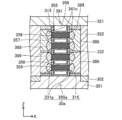
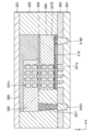
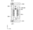
- FIGS. 16 to 19 are views showing a structure of a semiconductor device having a CFET.
- FIG. 16 is a sectional view in the X direction
- FIG. 17 is a sectional view of a gate portion in the Y direction
- FIG. 18 is a source/drain in the Y direction.
- FIG. 19 is a cross-sectional view of a part and a plan view.
- the X direction is the direction in which the nanowires extend
- the Y direction is the direction in which the gates extend
- the Z direction is the direction perpendicular to the substrate surface.
- FIGS. 16 to 19 are schematic views, and the dimensions and positions of the respective parts are not necessarily aligned.
- an element isolation region 302 is formed on the surface of a semiconductor substrate 301 such as a silicon (Si) substrate, and the element isolation region 302 defines an element active region 30a.
- the N-type FET is formed on the P-type FET.
- the stacked transistor structure 390a is formed on the semiconductor substrate 301.
- the stacked transistor structure 390a includes a gate structure 391 formed on the semiconductor substrate 301.
- the gate structure 391 includes a gate electrode 356, a plurality of nanowires 358, a gate insulating film 355, and an insulating film 357.
- the gate electrode 356 extends in the Y direction and rises in the Z direction.
- the nanowires 358 penetrate the gate electrode 356 in the X direction and are arranged in the Y direction and the Z direction.
- the gate insulating film 355 is formed between the gate electrode 356 and the nanowire 358.
- the gate electrode 356 and the gate insulating film 355 are formed at positions receding from both ends of the nanowire 358 in the X direction, and the insulating film 357 is formed at the receding portions.
- An insulating film 316 is formed on both sides of the insulating film 357 on the semiconductor substrate 301.
- Reference numerals 321 and 322 are interlayer insulating films.
- the gate electrode 356 is connected to the wiring in the upper layer by the via 385 provided in the opening 375.
- the gate electrode 356 titanium, titanium nitride, polycrystalline silicon, or the like can be used for the gate electrode 356.
- the gate insulating film 355 can be formed using a high dielectric constant material such as hafnium oxide, aluminum oxide, or oxides of hafnium and aluminum.
- silicon or the like can be used for the nanowire 358.
- silicon oxide, silicon nitride, or the like can be used for the insulating films 316 and 357.
- the number of nanowires 358 arranged in the Z direction is 4, and in the element active region 30a, the p-type semiconductor layer 331p is formed at each end of the two nanowires 358 on the semiconductor substrate 301 side. ..
- Two local wirings 386 that are in contact with the p-type semiconductor layer 331p are formed so as to sandwich the gate structure 391 in the X direction.
- an n-type semiconductor layer 341n is formed at each end of the two nanowires 358 on the side separated from the semiconductor substrate 301.
- Two local wirings 388 in contact with the n-type semiconductor layer 341n are formed so as to sandwich the gate structure 391 in the X direction.
- An insulating film 332 is formed between the local wiring 386 and the local wiring 388.
- An insulating film 389 is formed on the local wiring 388.
- the p-type semiconductor layer 331p is a p-type SiGe layer and the n-type semiconductor layer 341n is an n-type Si layer.
- the insulating film 332 can be formed using silicon oxide, silicon nitride, or the like.
- the local wiring 388 is connected to the embedded wiring 3101 via the via 3071.
- the local wiring 386 is connected to the embedded wiring 3102 via the via 3072.
- the laminated transistor structure 390a has a P-type FET including the gate electrode 356, the nanowire 358, the gate insulating film 355, and the P-type semiconductor layer 331p.
- one P-type semiconductor layer 331p functions as a source region
- the other P-type semiconductor layer 331p functions as a drain region
- the nanowire 358 functions as a channel.
- the stacked transistor structure 390a also has an N-type FET including a gate electrode 356, a nanowire 358, a gate insulating film 355, and an N-type semiconductor layer 341n.
- one N-type semiconductor layer 341n functions as a source region
- the other N-type semiconductor layer 341n functions as a drain region
- the nanowire 358 functions as a channel.
- wiring between transistors is performed by vias and metal wiring, but these can be realized by a known wiring process.
- the number of nanowires in the P-type FET and the N-type FET is assumed to be four in the Y direction and two in the Z direction, respectively, for a total of eight, but the number of nanowires is not limited to this. It is not something that can be done. Further, the number of nanowires in the P-type FET and the N-type FET may be different.
- a semiconductor layer portion that is formed at both ends of a nanowire and constitutes a terminal that serves as a source or a drain of a transistor is referred to as a “pad”.
- the p-type semiconductor layer 331p and the n-type semiconductor layer 341n correspond to pads.
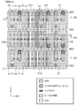
- FIG. 1 is a layout example of a lower portion of a circuit block using standard cells according to the first embodiment
- FIG. 2 is a layout example of an upper portion of a circuit block using standard cells according to the first embodiment
- FIG. 3 is a cross section taken along line X1-X1′ of FIG. 1 and FIG. 1 and 2 are plan views of the circuit block.
- FIG. 1 shows a portion including a three-dimensional structure transistor (here, P-type nanowire FET) formed on a lower portion, that is, a side closer to the substrate
- FIG. 2 shows an upper portion, that is, a portion farther from the substrate.
- a portion including a three-dimensional structure transistor here, N-type nanowire FET
- the horizontal direction of the drawing is the X direction (corresponding to the first direction)
- the vertical direction of the drawing is the Y direction (corresponding to the second direction)
- the direction perpendicular to the substrate surface is the same. It is set to the Z direction (corresponding to the depth direction).
- Dotted lines running vertically and horizontally in the plan view of FIG. 1 and the like indicate grids used for arranging components at the time of design.
- the grids are arranged at equal intervals in the X direction and at equal intervals in the Y direction.
- the grid spacing may be the same or different in the X and Y directions.
- a plurality of cells arranged in the X direction form a cell column CR. Then, the plurality of cell columns CR are arranged side by side in the Y direction.
- the plurality of cells include inverter cells C1 and C2 having a logic function of an inverter and filler cells C11, C12 and C12a having no logic function.
- the inverter cell C2 is arranged by inverting the inverter cell C1 in the Y direction.
- the filler cell C12a is arranged by inverting the filler cell C12 in the Y direction.
- the “filler cell” means a cell that has no logic function and does not contribute to the logic function of the circuit block, and is arranged between the logic cells.
- dummy pads are arranged in the filler cells.
- the “dummy pad” refers to a pad that does not contribute to the logical function of the circuit, in other words, a structure that has the same structure as the pad that constitutes the nanowire FET and that does not contribute to the logical function of the circuit block.
- the layout of the circuit block including the inverter cells C1 and C2 and the filler cells C11, C12, and C12a is illustrated.
- the actual layout is not limited to this, and any logic cell may be arranged.
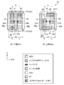
- FIG. 4 is a plan view showing the layout structure of the inverter cell. Specifically, FIGS. 4A and 4B are plan views of the inverter cell C1. Specifically, FIG. 4A shows the lower part and FIG. 4B shows the upper part.
- the inverter cell C1 is provided with power supply wirings 11 and 12 extending in the X direction at both ends in the Y direction.
- Both the power supply lines 11 and 12 are embedded power supply lines (BPR: Buried Power Rail) formed in the embedded wiring layer.
- the power supply wiring 11 supplies the power supply voltage VDD
- the power supply wiring 12 supplies the power supply voltage VSS.
- Wirings 71 and 72 extending in the X direction are formed in the M1 wiring layer.
- the wiring 71 corresponds to the input A and the wiring 72 corresponds to the output Y.
- a nanowire 21 extending in the X direction is formed below the inverter cell C1, and a nanowire 26 extending in the X direction is formed above the inverter cell C1.
- the nanowires 21 and 26 overlap each other in a plan view.
- Pads 22 a and 22 b doped with a P-type semiconductor are formed on both ends of the nanowire 21.
- N-type semiconductor-doped pads 27 a and 27 b are formed on both ends of the nanowire 26.
- the nanowire 21 constitutes a channel portion of the P-type transistor P1, and the pads 22a and 22b constitute terminals which are the source or the drain of the P-type transistor P1.
- the nanowire 26 forms a channel portion of the N-type transistor N1, and the pads 27a and 27b form a terminal that serves as a source or a drain of the N-type transistor N1.
- the N-type transistor N1 is formed at a position higher than the P-type transistor P1 in the Z direction.
- the gate wiring 31 extends in the Y direction at approximately the center in the X direction, and extends in the Z direction from the lower portion to the upper portion of the inverter cell C1.
- the gate wiring 31 becomes the gates of the P-type transistor P1 and the N-type transistor N1. That is, the nanowire 21, the gate wiring 31, and the pads 22a and 22b form the P-type transistor P1.
- the nanowire 26, the gate wiring 31, and the pads 27a and 27b form an N-type transistor N1.
- dummy gate wirings 35a and 35b are formed at both ends of the inverter cell C1 in the X direction, respectively. Like the gate line 31, the dummy gate lines 35a and 35b extend in the Y direction and the Z direction.
- the gate wiring 31 and the dummy gate wirings 35a and 35b are arranged at the same pitch L in the X direction.
- Local interconnects (LI) 41 and 42 extending in the Y direction are formed below the inverter cell C1.
- the local wiring 41 is connected to the pad 22a.
- the local wiring 42 is connected to the pad 22b.
- Local wirings 51 and 52 extending in the Y direction are formed above the inverter cell C1.
- the local wiring 51 is connected to the pad 27a.
- the local wiring 52 is connected to the pad 27b.
- the local wiring 41 extends to a position where it overlaps the power wiring 11 in a plan view, and is connected to the power wiring 11 via a contact 61.
- the contact 61 is formed at a position where the power supply wiring 11 and the local wiring 41 overlap each other in a plan view.
- the local wiring 51 extends to a position overlapping the power wiring 12 in a plan view, and is connected to the power wiring 12 via a contact 62.
- the contact 62 is formed at a position where the power supply wiring 12 and the local wiring 51 overlap each other in a plan view.
- the local wirings 42 and 52 are connected via a contact 63.
- the contact 63 is formed at a position where the local wiring 42 and the local wiring 52 overlap each other in a plan view.
- the wiring 71 (input A) is connected to the gate wiring 31 via the contact 81.
- the wiring 72 (output Y) is connected to the local wiring 52 via the contact 82.
- the inverter cell C1 has the P-type transistor P1 and the N-type transistor N1 and realizes an input A and output Y inverter circuit. That is, the inverter cell C1 is a standard cell having a logical function.
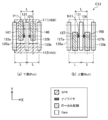
- FIG. 5 is a diagram showing the layout structure of the filler cell
- FIGS. 5A and 5B are plan views
- FIG. 6 is a cross-sectional view in the vertical direction in plan view.
- FIG. 5A shows the lower part of the filler cell C11
- FIG. 5B shows the upper part
- 6A is a cross section taken along line Y1-Y1′
- FIG. 6B is a cross section taken along line Y2-Y2′.
- the filler cell C11 is provided with power supply wirings 111 and 112 extending in the X direction at both ends in the Y direction.
- the power supply lines 111 and 112 are both embedded power supply lines (BPR) formed in the embedded wiring layer.
- the power supply wiring 111 supplies the same power supply voltage VDD as the power supply wiring 11.
- the power supply line 112 supplies the same power supply voltage VSS as the power supply line 12.
- Nanofibers 121 extending in the X direction are formed in the lower portion of the filler cell C11, and nanowires 126 extending in the X direction are formed in the upper portion of the filler cell C11.
- the nanowires 121 and 126 overlap in a plan view.
- Dummy pads 122a and 122b doped with a P-type semiconductor are formed on both ends of the nanowire 121.
- N-type semiconductor-doped dummy pads 127 a and 127 b are formed on both ends of the nanowire 126.
- the nanowire 121 constitutes a channel portion of the P-type dummy transistor P11, and the dummy pads 122a and 122b constitute terminals which are the source or the drain of the P-type dummy transistor P11.
- the nanowire 126 forms a channel portion of the N-type dummy transistor N11, and the dummy pads 127a and 127b form a terminal that is a source or a drain of the N-type dummy transistor N11.
- the N-type dummy transistor N11 is formed at a position higher than the P-type dummy transistor P11 in the Z direction.
- a dummy gate wiring 131 extending in the Y direction is formed substantially at the center in the X direction and extending in the Z direction from the lower portion to the upper portion of the filler cell C11.
- Dummy gate wirings 135a and 135b are formed at both ends of the filler cell C11 in the X direction.
- the dummy gate wirings 135a and 135b extend in the Y direction, and extend in the Z direction from the cell upper portion to the cell lower portion.
- the dummy gate wirings 131, 135a, 135b are arranged at the same pitch L in the X direction.
- the dummy gate wiring 131 becomes the gates of the P-type dummy transistor P11 and the N-type dummy transistor N11. That is, the nanowire 121, the dummy gate wiring 131, and the dummy pads 122a and 122b form the P-type dummy transistor P11. The nanowire 126, the dummy gate wiring 131, and the dummy pads 127a and 127b form an N-type dummy transistor N11.
- local wirings 141 and 142 extending in the Y direction are formed below the filler cell C11.
- the local wirings 141 and 142 respectively overlap the power supply wirings 111 and 112 in a plan view.
- the local wiring 141 is connected to the dummy pad 122a.
- the local wiring 142 is connected to the dummy pad 122b.
- the local wirings 151 and 152 extending in the Y direction are formed above the filler cell C11.
- the local wirings 151 and 152 respectively overlap the power supply wirings 111 and 112 in a plan view.
- the local wiring 151 is connected to the dummy pad 127a.
- the local wiring 152 is connected to the dummy pad 127b.
- the dummy gate wiring 131 and the local wirings 141, 142, 151, 152 are not connected to other wirings.
- the filler cell C11 has the P-type dummy transistor P11 and the N-type dummy transistor N11. Dummy pads 122a, 122b, 127a, 127b serving as sources and drains of the P-type dummy transistor P11 and the N-type dummy transistor N11 are connected to local wirings 141, 142, 151, 152, respectively. However, the local wirings 141, 142, 151, 152 are not connected to other wirings. That is, the filler cell C11 is a standard cell having no logic function.
- the inverter cell C1 and the filler cell C11 are arranged side by side in the X direction.
- the dummy gate wiring arranged at the boundary between the inverter cell C1 and the filler cell C11 corresponds to the dummy gate wiring 35b of the inverter cell C1 and the dummy gate wiring 135a of the filler cell C11.
- the nanowires 121 and 126 of the filler cell C11 are arranged at the same positions as the nanowires 21 and 26 of the inverter cell C1 in the Y direction, respectively.
- the nanowires 121 and 126 are arranged in the same layer as the nanowires 21 and 26 in the Z direction, respectively. That is, the P-type dummy transistor P11 and the N-type dummy transistor N11 of the filler cell C11 are arranged side by side with the P-type transistor P1 and the N-type transistor N1 of the inverter cell C1 in the X direction and in the Z direction, respectively. , Located in the same layer.
- the gate wiring 31, the dummy gate wiring 131, and the dummy gate wirings 35a, 35b (135a) and 135b are arranged at the same pitch L in the X direction. That is, the gate wiring 31, the dummy gate wiring 131, and the dummy gate wirings 35a, 35b (135a) and 135b are arranged in the X direction at equal widths, equal intervals, and equal pitches (pitch L).
- the local wirings 141 and 142 are arranged in the same layer as the local wirings 41 and 42 in the Z direction and at the same pitch L in the X direction. That is, the local wirings 41, 42, 141, 142 are arranged in the X direction at equal widths, equal intervals, and equal pitches (pitch L).
- the local wirings 151 and 152 are arranged in the same layer as the local wirings 51 and 52 in the Z direction and at the same pitch L in the X direction. That is, the local wirings 51, 52, 151, 152 are arranged in the X direction at equal widths, equal intervals, and equal pitches (pitch L).
- the filler cell C11 having no logic function is arranged adjacent to the inverter cell C1 having a logic function.
- the inverter cell C1 includes a P-type transistor P1 and an N-type transistor N1 arranged at a position higher than the P-type transistor P1 in the Z direction.
- the filler cell C11 includes a P-type dummy transistor P11 and an N-type dummy transistor N11.
- the nanowires 121 and 126 of the filler cell C11 are arranged at the same positions as the nanowires 21 and 26 of the inverter cell C1 in the Y direction, respectively.
- the P-type transistor P1 and the P-type dummy transistor P11 are arranged in the same layer in the Z direction.
- the N-type transistor N1 and the N-type dummy transistor N11 are arranged in the same layer in the Z direction. That is, by arranging the P-type and N-type dummy transistors in the filler cell C11, it is possible to suppress the density of transistor arrangement. As a result, manufacturing variations of the semiconductor integrated circuit device using the CFET can be suppressed and the yield can be improved.
- the transistors closest to the P-type transistor P1 and the N-type transistor N1 of the inverter cell C1 in the X direction are the P-type dummy transistor P11 and the N-type dummy transistor N11 of the filler cell C11, respectively. Therefore, in the P-type transistor P1 and the N-type transistor N1, the distance to the adjacent transistor is set to a predetermined value due to the existence of the P-type dummy transistor P11 and the N-type dummy transistor N11, respectively.
- the P-type dummy transistor P11 and the N-type dummy transistor N11 due to the presence of the P-type dummy transistor P11 and the N-type dummy transistor N11, from the transistor (P-type transistor P1 and N-type transistor N1) closest to the cell end of the logic cell (inverter cell C1) to the transistor adjacent to each of them.
- the distance can be estimated to a predetermined value. As a result, the accuracy of estimating the transistor performance of the logic cell can be improved.
- the gate wiring 31 of the inverter cell C1, the dummy gate wiring 131 of the filler cell C11 and the dummy gate wirings 35a, 35b (135a) and 135b are arranged at the same pitch L in the X direction. That is, the gate wiring 31, the dummy gate wiring 131, and the dummy gate wirings 35a, 35b (135a) and 135b are regularly arranged. As a result, in the semiconductor integrated circuit device using the CFET, manufacturing variations can be suppressed and the yield can be improved.
- the local wirings 141 and 142 of the filler cell C11 are arranged in the same layer as the local wirings 41 and 42 of the inverter cell C1 in the Z direction and at the same pitch L in the X direction. Further, the local wirings 151 and 152 of the filler cell C11 are arranged in the same layer as the local wirings 51 and 52 of the inverter cell C1 in the Z direction and at the same pitch L in the X direction. That is, the local wirings 41, 42, 141, 142 are regularly arranged. In addition, the local wirings 51, 52, 151 and 152 are regularly arranged. As a result, in the semiconductor integrated circuit device using the CFET, manufacturing variations can be suppressed and the yield can be improved.
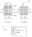
- FIG. 7 is a plan view showing another example of the filler cell according to this embodiment.
- FIG. 7A shows the lower part of the cell
- FIG. 7B shows the upper part of the cell.
- the filler cell C12 has a different cell width (dimension in the X direction) from the filler cell C11. That is, the cell width of the filler cell C11 is 2L, whereas the cell width of the filler cell C12 is 4L.
- nanowires 123a, 123b, 123c extending in the X direction are formed in the lower portion of the filler cell C12, and nanowires 128a, 128b, 128c extending in the X direction are formed in the upper portion of the filler cell C12. ing.
- the nanowires 123a, 123b, 123c respectively overlap with the nanowires 128a, 128b, 128c in a plan view.
- a dummy pad 124a doped with a P-type semiconductor is formed on the left side of the nanowire 123a in the drawing, and a dummy pad 124b doped with a P-type semiconductor is formed between the nanowires 123a and 123b.
- a dummy pad 124c doped with a P-type semiconductor is formed between the nanowires 123b and 123c, and a dummy pad 124d doped with a P-type semiconductor is formed on the right side of the nanowire 123c in the drawing.
- a dummy pad 129a doped with an N-type semiconductor is formed on the left side of the nanowire 128a in the drawing, and a dummy pad 129b doped with an N-type semiconductor is formed between the nanowires 128a and 128b.
- a dummy pad 129c doped with an N-type semiconductor is formed between the nanowires 128b and 128c, and a dummy pad 129d doped with an N-type semiconductor is formed on the right side of the nanowire 128c in the drawing.
- the nanowire 123a constitutes a channel portion of the P-type dummy transistor P12, and the dummy pads 124a and 124b constitute terminals which are the source or the drain of the P-type dummy transistor P12.
- the nanowire 123b constitutes the channel part of the P-type dummy transistor P13, and the dummy pads 124b and 124c constitute the terminal which becomes the source or the drain of the P-type dummy transistor P13.
- the nanowire 123c configures the channel portion of the P-type dummy transistor P14, and the dummy pads 124c and 124d configure the terminal that serves as the source or drain of the P-type dummy transistor P14.
- the nanowire 128a constitutes a channel portion of the N-type dummy transistor N12, and the dummy pads 129a and 129b constitute terminals which are sources or drains of the N-type dummy transistor N12.
- the nanowire 128b constitutes the channel part of the N-type dummy transistor N13, and the dummy pads 129b and 129c constitute the terminal which becomes the source or the drain of the N-type dummy transistor N13.
- the nanowire 128c forms a channel portion of the N-type dummy transistor N14, and the dummy pads 129c and 129d form a terminal serving as a source or a drain of the N-type dummy transistor N14.
- dummy gate wirings 135a and 135b extending in the Y direction and extending in the Z direction from the lower portion to the upper portion of the cell are formed at both ends of the filler cell C12 in the X direction.
- dummy gate wirings 132a, 132b and 132c extending in the Y direction and extending in the Z direction from the lower portion to the upper portion of the cell are formed at a pitch L.
- the dummy gate wiring 132a becomes the gates of the P-type dummy transistor P12 and the N-type dummy transistor N12.
- the dummy gate wiring 132b becomes the gates of the P-type dummy transistor P13 and the N-type dummy transistor N13.
- the dummy gate wiring 132c becomes the gates of the P-type dummy transistor P14 and the N-type dummy transistor N14. That is, the nanowire 123a, the dummy gate wiring 132a, and the dummy pads 124a and 124b form the P-type dummy transistor P12.
- the nanowire 123b, the dummy gate wiring 132b, and the dummy pads 124b and 124c form a P-type dummy transistor P13.
- the nanowire 123c, the dummy gate wiring 132c, and the dummy pads 124c and 124d form a P-type dummy transistor P14.
- the nanowire 128a, the dummy gate wiring 132a, and the dummy pads 129a and 129b form an N-type dummy transistor N12.
- the nanowire 128b, the dummy gate wiring 132b, and the dummy pads 129b and 129c form an N-type dummy transistor N13.
- the nanowire 128c, the dummy gate wiring 132c, and the dummy pads 129c and 129d form an N-type dummy transistor N14.
- local wirings 143 to 146 extending in the Y direction are formed below the filler cell C12. Each of the local wirings 143 to 146 overlaps with the power supply wirings 111 and 112 in a plan view.
- the local wirings 143 to 146 are connected to the dummy pads 124a to 124d, respectively.
- the local wirings 143-146 are arranged at the same pitch L in the X direction and in the same layer in the Z direction.
- local wirings 153 to 156 extending in the Y direction are formed above the filler cell C12.
- the local wirings 153 to 156 respectively overlap the power supply wirings 111 and 112 in plan view.
- the local wirings 153 to 156 are connected to the dummy pads 129a to 129d, respectively.
- the local wirings 153 to 156 are arranged at the same pitch L in the X direction and in the same layer in the Z direction.
- the dummy gate wirings 132a to 132c and the local wirings 143 to 146 and 153 to 156 are not connected to other wirings.
- the filler cell C12 has the P-type dummy transistors P12 to P14 and the N-type dummy transistors N12 to N14.
- the dummy pads 124a to 124d and 129a to 129d which are the sources and drains of the P type dummy transistors P12 to P14 and the N type dummy transistors N12 to N14, are connected to the local wirings 143 to 146 and the local wirings 153 to 156, respectively.
- the local wirings 143 to 146 and the local wirings 153 to 156 are not connected to other wirings or the like. That is, the filler cell C12 is a standard cell having no logic function.
- the filler cell C12 is arranged adjacent to the inverter cell C1 as shown in the circuit blocks of FIGS. 1 and 2.
- the nanowires 123a, 123b, 123c of the filler cell C12 are arranged at the same position in the Y direction as the nanowires 21 of the inverter cell C1 and in the same layer in the Z direction.
- the nanowires 128a, 128b, 128c of the filler cell C12 are arranged at the same position in the Y direction and the same layer in the Z direction as the nanowire 26 of the inverter cell C1.
- the P-type dummy transistors P12, P13, P14 of the filler cell C12 are arranged side by side with the P-type transistor P1 of the inverter cell C1 in the X direction and in the same layer in the Z direction.
- the N-type transistors N12, N13, N14 of the filler cell C12 are arranged side by side in the X direction and the N-type transistor N1 of the inverter cell C1 and in the same layer in the Z direction.
- the gate wiring 31, the dummy gate wirings 132a, 132b, 132c, and the dummy gate wirings 35a, 35b (135a), 135b are arranged at the same pitch L in the X direction. That is, the gate wiring 31, the dummy gate wirings 132a, 132b, 132c, and the dummy gate wirings 35a, 35b (135a), 135b are arranged in the X direction at equal widths, equal intervals, and equal pitches.
- the local wirings 143-146 are arranged at the same pitch L as the local wirings 41 and 42 of the inverter cell C1 in the X direction and in the same layer in the Z direction. That is, the local wirings 41, 42, 143 to 146 are arranged in the X direction at equal widths, equal intervals, and equal pitches (pitch L).
- the local wirings 153 to 156 are arranged at the same pitch L in the X direction as the local wirings 51 and 52 of the inverter cell C1 and in the same layer in the Z direction. That is, the local wirings 51, 52, 153 to 156 are arranged in the X direction at equal widths, equal intervals, and equal pitches (pitch L).
- the filler cell C12 according to this modification can obtain the same effect as the filler cell C11. Note that filler cells having cell widths other than 2L and 4L can be similarly configured.
- FIG. 8 is a plan view showing another example of the layout structure of the filler cell according to the first embodiment.
- FIG. 8A shows the lower part of the cell
- FIG. 8B shows the upper part of the cell.
- the filler cell C13 has basically the same configuration as the filler cell C11 shown in FIG. 5, but the length of each local wiring in the Y direction is different. That is, the local wirings 147 and 148 extend in the Y direction to a position overlapping the power supply wiring 111 in a plan view, but do not overlap the power supply wiring 112. Further, the local wirings 157 and 158 extend in the Y direction to a position overlapping the power supply wiring 112 in plan view, but do not overlap the power supply wiring 111.
- the filler cell C13 according to this modification can obtain the same effect as the filler cell C11.
- the local wirings 147 and 148 each overlap the power supply wiring 111 in a plan view, and the local wirings 157 and 158 respectively overlap the power supply wiring 112 in a plan view. Not limited to The local wirings 147 and 148 may not overlap the power supply wiring 111 and may overlap the power supply wiring 112 in plan view. Further, each of the local wirings 157 and 158 overlaps with the power supply wiring 111 in plan view, and may not overlap with the power supply wiring 112. In addition, the local wirings 147, 148, 157, and 158 may not overlap each of the power supply wirings 111 and 112 in a plan view. However, at least one of the local wirings 147, 148, 157, and 158 overlaps the power supply wiring 111 or the power supply wiring 112 in a plan view.
- FIG. 9 is a plan view showing another example of the layout structure of the filler cell according to the first embodiment.
- 9A shows the lower part of the cell
- FIG. 9B shows the upper part of the cell.
- the local wiring is not connected to any of the dummy pads 122a, 122b, 127a, 127b.
- Other configurations are similar to those of the filler cell C11.
- the nanowires 121 and 126 are arranged at the same positions as the nanowires 21 and 26 of the inverter cell C1 in the Y direction, respectively.
- the P-type dummy transistor P11 of the filler cell C14 is arranged in the same layer as the P-type transistor P1 of the inverter cell C1 in the Z direction.
- the N-type dummy transistor N11 of the filler cell C14 is arranged in the same layer as the N-type transistor N1 of the inverter cell C1 in the Z direction. That is, by arranging the P-type and N-type dummy transistors in the filler cell C14, the density of transistor arrangement can be suppressed. As a result, manufacturing variations of the semiconductor integrated circuit device using the CFET can be suppressed and the yield can be improved.
- the gate wiring 31 of the inverter cell C1, the dummy gate wiring 131 of the filler cell C14, and the dummy gate wirings 35a, 35b (135a) and 135b are arranged at the same pitch L in the X direction. That is, the gate wiring 31, the dummy gate wiring 131, and the dummy gate wirings 35a, 35b (135a) and 135b are regularly arranged. As a result, manufacturing variations of the semiconductor integrated circuit device using the CFET can be suppressed, and the yield can be improved.
- the transistors closest to the P-type transistor P1 and the N-type transistor N1 of the inverter cell C1 in the X direction are the P-type dummy transistor P11 and the N-type dummy transistor N11 of the filler cell C14, respectively. Therefore, in the P-type transistor P1 and the N-type transistor N1, the distance to the adjacent transistor is set to a predetermined value due to the existence of the P-type dummy transistor P11 and the N-type dummy transistor N11, respectively.
- the local wiring is not connected to any of the dummy pads 122a, 122b, 127a, 127b, but the present invention is not limited to this. Local wirings extending in the Y direction may be connected to some of the dummy pads 122a, 122b, 127a, 127b. Further, the local wirings connected to the dummy pads 122a, 122b, 127a, 127b may or may not overlap the power supply wirings 111, 112 in plan view.
- FIG. 10 is a plan view showing another example of the layout structure of the filler cell according to the first embodiment.
- FIG. 10A shows the lower portion of the cell
- FIG. 10B shows the upper portion of the cell.
- the filler cell C15 has basically the same configuration as the filler cell C11 shown in FIG. 4, but the local wiring and the power supply wiring are connected via a contact.
- contacts 161-164 extending in the Z direction are formed. Each of the contacts 161 to 164 is arranged at a position overlapping the power supply wiring 111 in plan view.
- the power supply wiring 111 and the local wiring 141 are connected to each other via a contact 161.
- the power supply wiring 111 and the local wiring 142 are connected to each other via a contact 162.
- the local wirings 141 and 151 are connected to each other via a contact 163.
- the local wirings 142 and 152 are connected to each other via a contact 164.
- the filler cell C15 according to this modification can obtain the same effect as that of the filler cell C11.
- the dummy pad 122a, 122b, 127a, 127b is supplied with the power supply voltage VDD from the power supply wire 111 via the local wires 141, 142, 151, 152 and the contacts 161-164. That is, the source and drain of the P-type dummy transistor P11 and the source and drain of the N-type dummy transistor N11 are fixed to the same potential VDD. As a result, the floating nodes of the P-type and N-type dummy transistors can be reduced, and the operation of the circuit block can be stabilized.
- the power supply wiring 111 or the power supply wiring 112 and the dummy gate wiring 131 may be connected via a contact to fix the potential of the dummy gate wiring 131.
- the local wirings 141, 142, 151, 152 are connected to the power supply wiring 111 via the contacts 161-164, but the invention is not limited to this.
- the local wirings 141, 142, 151, 152 may be connected to the power supply wiring 112 via contacts.
- the local wirings 141, 142, 151, 152 may not have the power wiring 112 overlapping with each other in plan view.
- FIG. 11 is a plan view showing another example of the layout structure of the filler cell according to the first embodiment.
- FIG. 11A shows the lower part of the cell
- FIG. 11B shows the upper part of the cell.
- the filler cell C16 has basically the same configuration as the filler cell C11 shown in FIG. 5, but the length of the local wiring in the lower portion of the cell in the Y direction is different, and the local wiring and the power wiring are different from each other. Are connected via contacts.
- Local wires 149 and 150 extending in the Y direction are formed in the lower portion of the cell.
- the local wiring 149 is connected to the dummy pad 122a.
- the local wiring 150 is connected to the dummy pad 122b.
- Each of the local wirings 149 and 150 overlaps the power supply wiring 111, but does not overlap the power supply wiring 112 in a plan view.
- contacts 165-168 extending in the Z direction are formed.
- the contacts 165 and 166 overlap the power supply wiring 111 in a plan view.
- the contacts 167 and 168 overlap the power supply wiring 112 in a plan view.
- the power supply wiring 111 and the local wiring 149 are connected to each other via a contact 165.
- the power supply wiring 111 and the local wiring 150 are connected to each other via a contact 166.
- the power supply wiring 112 and the local wiring 151 are connected to each other via a contact 167.
- the power supply wiring 112 and the local wiring 152 are connected to each other via a contact 168.
- the filler cell C16 according to this modification can obtain the same effect as the filler cell C11.
- the power supply voltage VDD is supplied to the dummy pads 122a and 122b from the power supply wiring 111 via the local wirings 149 and 150 and the contacts 165 and 166, respectively.
- the power supply voltage VSS is supplied from the power supply wiring 112 to the dummy pads 127a and 127b via the local wirings 151 and 152 and the contacts 167 and 168, respectively. That is, the source and drain of the P-type dummy transistor P11 are both fixed at the potential VDD. Further, the source and drain of the N-type dummy transistor N11 are both fixed at the potential VSS. As a result, the floating nodes of the P-type and N-type dummy transistors can be reduced, and the operation of the circuit block can be stabilized.
- the power supply voltage VDD is supplied from the power supply wiring 111 to the local wirings 149 and 150 arranged below the filler cell C16 through the contacts 165 and 166.
- the power supply voltage VSS is supplied from the power supply wire 112 to the local wires 151 and 152 arranged above the filler cell C16 via the contacts 167 and 168. That is, wiring capacitance is generated between the local wiring 149 and the local wiring 151 that overlap in a plan view, and between the local wiring 150 and the local wiring 152 that overlap in a plan view. Since this wiring capacitance causes a capacitance between power supplies, the power supply potential supplied to the circuit block is stabilized.
- the local wirings 149 and 150 are connected to the power supply wiring 111 through the contacts 165 and 166, and the local wirings 151 and 152 are connected to the power supply wiring 112 through the contacts 167 and 168. , But not limited to this.
- the local wirings 149 and 150 may be connected to the power supply wiring 112, and the local wirings 151 and 152 may be connected to the power supply wiring 111. In this case, the local wirings 149 and 150 do not overlap with the power supply wiring 111 in plan view, but do overlap with the power supply wiring 112.
- the local wirings 151 and 152 may not overlap the power supply wiring 111 in plan view.
- FIG. 12A and 12B are views showing a layout structure of a filler cell according to the second embodiment.
- FIG. 12A shows a cell lower part and
- FIG. 12B shows a cell upper part.
- Filler cell C21 does not have P-type and N-type dummy transistors.
- power supply wirings 211 and 212 extending in the X direction are provided at both ends in the Y direction. Both the power supply lines 211 and 212 are embedded power supply lines (BPR) formed in the embedded wiring layer.
- the power supply wiring 211 supplies the same power supply voltage VDD as the power supply wiring 11.
- the power supply line 212 supplies the same power supply voltage VSS as that of the power supply line 12.
- a dummy gate wiring 231 extending in the Y direction is formed substantially at the center in the X direction and extending in the Z direction from the upper portion to the lower portion of the cell.
- Dummy gate wirings 235a and 235b extending in the Y direction and extending in the Z direction from the upper portion to the lower portion of the cell are formed at both ends of the filler cell C21 in the X direction.
- the dummy gate wirings 231, 235a, 235b are arranged at the same pitch L in the X direction.
- ⁇ Local cells 241 and 242 extending in the Y direction are formed in the lower portion of the cell.
- the local wirings 241 and 242 have an overlap with the power supply wirings 211 and 212 in plan view, respectively.
- the local wiring 241 is arranged between the dummy gate wirings 231 and 235a in plan view.
- the local wiring 242 is arranged between the dummy gate wirings 231 and 235b in plan view.
- -Local wirings 251 and 252 extending in the Y direction are formed in the upper part of the cell.
- the local wirings 251 and 252 have an overlap with the power supply wirings 211 and 212 in plan view, respectively.
- the local wiring 251 is arranged between the dummy gate wirings 231 and 235a in plan view.
- the local wiring 252 is arranged between the dummy gate wirings 231 and 235b in plan view.
- the dummy gate wiring 231 and the local wirings 241, 242, 251, 252 are not connected to any other wiring.
- the filler cell C21 the nanowire and the dummy pad are not provided, and the P-type dummy transistor and the N-type dummy transistor are not formed. That is, the filler cell C21 is a standard cell having no logic function.
- the filler cell C21 is arranged adjacent to the inverter cell C1.
- the dummy gate wiring arranged at the boundary between the inverter cell C1 and the filler cell C21 corresponds to the dummy gate wiring 35b of the inverter cell C1 and the dummy gate wiring 235a of the filler cell C21.
- the gate wiring 31 of the inverter cell C1, the dummy gate wiring 231 of the filler cell C21, and the dummy gate wirings 35a, 35b (235a), 235b are arranged at the same pitch L in the X direction. That is, the gate wiring 31, the dummy gate wiring 231, and the dummy gate wirings 35a, 35b (235a), 235b are arranged in the X direction at equal widths, equal intervals, and equal pitches.
- the local wirings 241 and 242 are arranged in the same layer as the local wirings 41 and 42 of the inverter cell C1 in the Z direction and at the same pitch L in the X direction. That is, the local wirings 41, 42, 241, 242 are arranged in the X direction at equal widths, equal intervals, and equal pitches (pitch L).
- the local wirings 251 and 252 are arranged in the same layer as the local wirings 51 and 52 of the inverter cell C1 in the Z direction and at the pitch L in the X direction. That is, the local wirings 51, 52, 251, 252 are arranged in the X direction at equal widths, equal intervals, and equal pitches (pitch L).
- the filler cell C21 having no logic function is arranged adjacent to the inverter cell C1 having a logic function.
- the local wirings 241 and 242 of the filler cell C21 are arranged in the same layer as the local wirings 41 and 42 of the inverter cell C1 in the Z direction.
- the local wirings 251 and 252 of the filler cell C21 are arranged in the same layer as the local wirings 51 and 52 of the inverter cell C1 in the Z direction. That is, the local wirings 41, 42, 241, 242 are regularly arranged. Further, the local wirings 51, 52, 251, 252 are regularly arranged.
- the local wirings 41, 42, 241, 242 are arranged at the same pitch L in the X direction.
- the local wirings 51, 52, 251, 252 are arranged at the same pitch L in the X direction. That is, the local wirings 41, 42, 241, 242 are regularly arranged. Further, the local wirings 51, 52, 251, 252 are regularly arranged. As a result, in the semiconductor integrated circuit device using the CFET, manufacturing variations can be suppressed and the yield can be improved.
- the dummy gate wiring 231 of the filler cell C21, the gate wiring 31 of the inverter cell C1, and the dummy gate wirings 35a, 35b (235a) and 235b are arranged at the same pitch L in the X direction. That is, the gate wiring 31, the dummy gate wiring 231, and the dummy gate wirings 35a, 35b (235a), 235b are regularly arranged. As a result, in the semiconductor integrated circuit device using the CFET, manufacturing variations can be suppressed and the yield can be improved.
- the local wirings 241, 242, 251, 252 have an overlap with the power supply wirings 211, 212 in a plan view, but the invention is not limited to this. Each of the local wirings 241, 242, 251, 252 does not have to overlap with any one of them.
- FIG. 13A and 13B are diagrams showing another layout structure of the filler cell according to the second embodiment.
- FIG. 13A shows a cell lower part and
- FIG. 13B shows a cell upper part.
- the filler cell C22 has a different cell width in the X direction from the filler cell C21. That is, the cell width of the filler cell C21 is 2L, while the cell width of the filler cell C22 is L.
- a local wiring 243 extending in the Y direction is formed in the lower part of the cell, approximately in the center in the X direction.
- a local wiring 253 extending in the Y direction is formed at an approximately central portion in the X direction in the upper portion of the cell.
- the local wirings 243 and 253 respectively overlap the power supply wirings 211 and 212 in a plan view.
- the local wiring 243 is arranged in the same layer as the local wirings 41 and 42 of the inverter cell C1 in the Z direction and has the same pitch in the X direction. It is placed at L.
- the local wirings 253 are arranged in the same layer as the local wirings 51 and 52 of the inverter cell C1 in the Z direction and at the same pitch L in the X direction.
- the local wiring 243 is arranged in the same layer as the local wirings 41 and 42 of the inverter cell C1 in the Z direction.
- the local wiring 253 is arranged in the same layer as the local wirings 51 and 52 of the inverter cell C1 in the Z direction. That is, the local wirings 41, 42, 243 are regularly arranged. Further, the local wirings 51, 52, 253 are regularly arranged. As a result, in the semiconductor integrated circuit device using the CFET, manufacturing variations can be suppressed and the yield can be improved.
- the local wirings 41, 42, 243 are arranged at the same pitch L in the X direction.
- the local wirings 51, 52, 253 are arranged at the same pitch L in the X direction. That is, the local wirings 41, 42, 243 are regularly arranged. Further, the local wirings 51, 52, 253 are regularly arranged. As a result, in the semiconductor integrated circuit device using the CFET, manufacturing variations can be suppressed and the yield can be improved.
- the filler cell can be arranged in a very small gap such that the logical cell spacing is L.
- Part 2 14A and 14B are diagrams showing another layout structure of the filler cell according to the second embodiment.
- FIG. 14A shows a cell lower portion and
- FIG. 14B shows a cell upper portion.
- the filler cell C23 has basically the same configuration as the filler cell C21 shown in FIG. 12, but the local wiring and the power supply wiring are connected by a contact.
- contacts 261 to 264 extending in the Z direction are formed. Each of the contacts 261 to 264 is arranged at a position overlapping the power supply wiring 211 in plan view.
- the power supply wiring 211 and the local wiring 241 are connected to each other via a contact 261.
- the power supply wiring 211 and the local wiring 242 are connected to each other via a contact 262.
- the local wirings 241 and 251 are connected to each other via a contact 263.
- the local wirings 242 and 252 are connected to each other via a contact 264.
- the same power supply voltage VDD is supplied to the local wirings 241, 242, 251, 252 from the power supply wiring 211 via the contacts 261 to 264, respectively. That is, the local wirings 241, 242, 251, 252 are all fixed at the same potential VDD. As a result, the number of floating nodes can be reduced and the operation of the circuit block can be stabilized.
- the power supply wiring 211 or the power supply wiring 212 and the dummy gate wiring 231 may be connected by a contact to fix the potential of the dummy gate wiring 231.
- the local wirings 241, 242, 251, 252 are connected to the power supply wiring 211 via the contacts 261 to 264, but the invention is not limited to this.
- the local wirings 241, 242, 251, 252 may be connected to the power supply wiring 212 via contacts.
- the filler cell C23 is a standard cell having a cell width of 2 L, but it is not limited to this, and the cell width of the filler cell C23 may be L. In this case, the dummy gate wiring 231, the local wirings 242 and 252, and the contacts 262 and 264 are unnecessary.
- FIG. 15A and 15B are views showing another layout structure of the filler cell according to the second embodiment.
- FIG. 15A shows a cell lower part
- FIG. 15B shows a cell upper part.
- the filler cell C24 has basically the same configuration as the filler cell C21 shown in FIG. 12, except that the local wiring and the power supply wiring are connected by a contact, and the length of the local wiring in the lower part of the cell in the Y direction. Are different.
- the local wirings 244 and 245 respectively overlap the power supply wiring 211, but do not overlap the power supply wiring 212 in plan view.
- contacts 265 to 268 extending in the Z direction are formed.
- the contacts 265, 266 are arranged at positions overlapping the power supply wiring 211 in a plan view
- the contacts 267, 268 are arranged at positions overlapping the power supply wiring 212 in a plan view.
- the power supply wiring 211 and the local wiring 244 are connected to each other via a contact 265.
- the power supply wiring 211 and the local wiring 245 are connected to each other via a contact 266.
- the power supply wiring 212 and the local wiring 251 are connected to each other via a contact 267.
- the power supply wiring 212 and the local wiring 252 are connected to each other via a contact 268.
- the filler cell C22 according to this modification can obtain the same effect as the filler cell C21.
- the power supply voltage VDD is supplied to the local wirings 244 and 245 from the power supply wiring 211 via the contacts 265 and 266.
- the power supply voltage VSS is supplied to the local wirings 251 and 252 from the power supply wiring 212 through the contacts 267 and 268. That is, the local wirings 244 and 245 are both fixed at the potential VDD, and the local wirings 251 and 252 are both fixed at the potential VSS. As a result, the number of floating nodes can be reduced and the operation of the circuit block can be stabilized.
- Wiring capacitance is generated between the local wiring 244 and the local wiring 251 that overlap in a plan view and between the local wiring 245 and the local wiring 252 that overlap in a plan view. Since this wiring capacitance causes a capacitance between power supplies, the power supply potential supplied to the circuit block is stabilized.
- the local wirings 244 and 245 are connected to the power supply wiring 211 via the contacts 265 and 266, and the local wirings 251 and 252 are connected to the power supply wiring 212 via the contacts 267 and 268. , But not limited to this.
- the local wirings 244 and 245 may be connected to the power supply wiring 212, and the local wirings 251 and 252 may be connected to the power supply wiring 211. In this case, the local wirings 244 and 245 do not overlap with the power supply wiring 211 in plan view, but do overlap with the power supply wiring 212.
- the filler cell C24 is a standard cell having a cell width of 2 L, but the present invention is not limited to this, and the cell width of the filler cell C24 may be L. In this case, the dummy gate wiring 231, the local wirings 245, 252 and the contacts 266, 268 are unnecessary.
- the transistor is provided with one nanowire in each of the cell upper portion and the cell lower portion, but a part or all of the transistor may be provided with a plurality of nanowires. ..
- a plurality of nanowires may be provided in the Y direction in a plan view, or a plurality of nanowires may be provided in the Z direction.
- a plurality of nanowires may be provided in each of the Y direction and the Z direction.
- the number of nanowires included in the transistor may be different between the upper portion and the lower portion of the cell.
- the nanowire FET is described as an example of the three-dimensional structure transistor, but the present invention is not limited to this.
- the transistor formed under each filler cell may be a fin-type transistor.
- the cross-sectional shape of the nanowires 121 and 126 in the vertical direction in plan view is illustrated as a square, but the shape is not limited to this.
- the cross-sectional shape of the nanowires 121 and 126 in the vertical direction in plan view may be a shape other than a square (for example, a rectangle).
- a P-type transistor is formed in the lower portion of the cell and an N-type transistor is formed in the upper portion of the cell.
- Type transistors may be formed.
- the power supply wirings 11, 12, 111, 112, 211, 212 are embedded wirings, but are not limited to this.
- the power supply wirings 11, 12, 111, 112, 211 and 212 may be arranged in the M1 wiring layer.
- the present disclosure can be applied to a semiconductor integrated circuit including a standard cell using a CFET, and is useful for improving the performance of a semiconductor chip, for example.
Landscapes
- Design And Manufacture Of Integrated Circuits (AREA)
- Semiconductor Integrated Circuits (AREA)
Abstract
論理機能を有するインバータセル(C1)と論理機能を有さないフィラーセル(C11)とが隣接して配置される。フィラーセル(C11)のナノワイヤ(122,126)は、それぞれ、Y方向において、インバータセル(C1)のナノワイヤ(22,26)と同じ位置に配置される。また、フィラーセル(C11)のP型ダミートランジスタ(P11)およびN型ダミートランジスタ(N11)は、それぞれ、Z方向において、P型トランジスタ(P1)およびN型トランジスタ(N1)と同層に配置される。
Description
本開示は、立体構造トランジスタを含むスタンダードセル(以下、適宜、単にセルともいう)を備えた半導体集積回路装置に関するものである。
半導体基板上に半導体集積回路を形成する方法として、スタンダードセル方式が知られている。スタンダードセル方式とは、特定の論理機能を有する基本的単位(例えば、インバータ,ラッチ,フリップフロップ,全加算器など)をスタンダードセルとして予め用意しておき、半導体基板上に複数のスタンダードセルを配置して、それらのスタンダードセルを配線で接続することによって、LSIチップを設計する方式のことである。
また、LSIの基本構成要素であるトランジスタは、ゲート長の縮小(スケーリング)により、集積度の向上、動作電圧の低減、および動作速度の向上を実現してきた。しかし近年、過度なスケーリングによるオフ電流と、それによる消費電力の著しい増大が問題となっている。この問題を解決するため、トランジスタ構造を従来の平面型から立体型に変更した立体構造トランジスタが盛んに研究されている。
非特許文献1,2では、新規デバイスとして、立体構造のP型FETとN型FETを基板に対して垂直方向に積層した立体構造デバイスと、これを用いたスタンダードセルが開示されている。
Ryckaert J. et al., "The Complementary FET (CFET) for CMOS scaling beyond N3", 2018 Symposium on VLSI Technology Digest of Technical Papers
A. Mocuta et al., "Enabling CMOS Scaling Towards 3nm and Beyond", 2018 Symposium on VLSI Technology Digest of Technical Papers
本明細書では、立体構造のP型FETとN型FETを基板に対して垂直方向に積層した立体構造デバイスのことを、非特許文献1の記載にならい、CFET(Complementary FET)と呼ぶことにする。また、基板に対して垂直をなす方向のことを、深さ方向と呼ぶ。
ここで、スタンダードセルには、例えば、NANDゲート、NORゲート等の論理機能を有するセル(以下、適宜、論理セルという)の他に、論理機能を有さないセルが含まれる。論理機能を有さないセルとして、「フィラーセル」が挙げられる。「フィラーセル」とは、論理機能を有さず、回路ブロックの論理機能に寄与せず、論理セルの間に配置されたセルのことをいう。
これまで、CFETを用いたフィラーセルの構造や、CFETを用いたフィラーセルを含む半導体集積回路のレイアウトに関して、具体的な検討はまだなされていない。
本開示は、CFETを用いたフィラーセルを含む半導体集積回路装置のレイアウトを提供するものである。
本開示の第1態様では、論理機能を有する第1スタンダードセルと、前記第1スタンダードセルに隣接して配置され、論理機能を有さない第2スタンダードセルと、を備える半導体集積回路装置であって、前記第1スタンダードセルは、第1方向に延伸され、第1電源電圧を供給する第1電源配線と、前記第1方向に延伸され、前記第1電源電圧と異なる第2電源電圧を供給する第2電源配線と、第1導電型の立体構造トランジスタである、第1トランジスタと、深さ方向において前記第1トランジスタよりも高い位置に形成され、かつ、平面視において、チャネル部が前記第1トランジスタのチャネル部と重なりを有する位置に配置された第2導電型の立体構造トランジスタである、第2トランジスタと、を備え、前記第2スタンダードセルは、前記第1方向に延伸され、前記第1電源電圧を供給する第3電源配線と、前記第1方向に延伸され、前記第2電源電圧を供給する第4電源配線と、前記第1方向と垂直をなす第2方向において、チャネル部が前記第1トランジスタのチャネル部と同じ位置に配置され、かつ、深さ方向において、前記第1トランジスタと同層に配置された前記第1導電型の立体構造トランジスタである、第1ダミートランジスタと、前記第2方向において、チャネル部が前記第2トランジスタのチャネル部と同じ位置に配置され、かつ、前記深さ方向において、前記第2トランジスタと同層に配置された前記第2導電型の立体構造トランジスタである、第2ダミートランジスタと、を備える。
この態様によると、第1トランジスタおよび第1ダミートランジスタのチャネル部は、第2方向において、同じ位置に配置される。第1トランジスタおよび第1ダミートランジスタは、深さ方向において、同層に配置される。また、第2トランジスタおよび第2ダミートランジスタのチャネル部は、第2方向において、同じ位置に配置される。第2トランジスタおよび第2ダミートランジスタは、深さ方向において、同層に配置される。すなわち、第2スタンダードセルに第1および第2トランジスタを配置することにより、トランジスタ配置の粗密を抑制することができる。これにより、半導体集積回路装置の製造ばらつきを抑えることができ、歩留まりを向上させることができる。
本開示の第2態様では、論理機能を有する第1スタンダードセルと、前記第1スタンダードセルに隣接して配置され、論理機能を有さない第2スタンダードセルと、を備える半導体集積回路装置であって、前記第1スタンダードセルは、第1方向に延伸され、第1電源電圧を供給する第1電源配線と、前記第1方向に延伸され、前記第1電源電圧と異なる第2電源電圧を供給する第2電源配線と、第1導電型の立体構造トランジスタである、第1トランジスタと、深さ方向において、前記第1トランジスタよりも高い位置に形成され、かつ、平面視において、チャネル部が前記第1トランジスタのチャネル部と重なりを有する位置に配置された第2導電型の立体構造トランジスタである、第2トランジスタと、前記第1方向と垂直をなす第2方向に延び、前記第1トランジスタのソースおよびドレインにそれぞれ接続された第1および第2ローカル配線と、前記第2方向に延び、前記第2トランジスタのソースおよびドレインにそれぞれ接続された第3および第4ローカル配線と、を備え、前記第2スタンダードセルは、前記第1方向に延伸され、前記第1電源電圧を供給する第3電源配線と、前記第1方向に延伸され、前記第2電源電圧を供給する第4電源配線と、前記深さ方向において、前記第1および第2ローカル配線と同層に配置された第5ローカル配線と、前記深さ方向において、前記第3および第4ローカル配線と同層に配置された第6ローカル配線とを備え、前記第5および第6ローカル配線のうち少なくともいずれか一方は、平面視で、前記第3および第4電源配線と重なりを有している。
この態様によると、第1スタンダードセルと第2スタンダードセルとは、隣接して配置される。また、第1,第2および第5ローカル配線は、同層に配置される。第3,第4および第6ローカル配線は、同層に配置される。すなわち、半導体集積回路装置の下部において、第1,第2および第5ローカル配線は、規則的に配置される。また、半導体集積回路装置の上部において、第3,第4および第6ローカル配線は、規則的に配置される。これにより、半導体集積回路装置の製造ばらつきを抑えることができ、歩留まりを向上させ
ることができる。
ることができる。
本開示によると、CFETを用いた半導体集積回路装置において、製造や性能のばらつきを抑制できるとともに、歩留まりを向上させることができる。
以下、実施の形態について、図面を参照して説明する。以下の実施の形態では、半導体集積回路装置は複数のスタンダードセル(本明細書では、適宜、単にセルという)を備えており、この複数のスタンダードセルのうち少なくとも一部は、CFET、すなわち、立体構造のP型FETとN型FETを基板に対して垂直方向に積層した立体構造デバイスを備えるものとする。
まず、CFETの基本構造について説明する。図16~図19はCFETを備えた半導体装置の構造を示す図であり、図16はX方向における断面図、図17はY方向におけるゲート部分の断面図、図18はY方向におけるソース・ドレイン部分の断面図、図19は平面図である。なお、X方向はナノワイヤが延びる方向、Y方向はゲートが延びる方向、Z方向は基板面と垂直をなす方向としている。また、図16~図19は概略図であり、各部の寸法や位置等は必ずしも整合していない。
この半導体装置では、シリコン(Si)基板等の半導体基板301の表面に素子分離領域302が形成されており、素子分離領域302により、素子活性領域30aが画定されている。素子活性領域30aでは、P型FET上にN型FETが形成されている。
素子活性領域30aでは、半導体基板301上に積層トランジスタ構造390aが形成されている。積層トランジスタ構造390aは、半導体基板301上に形成されたゲート構造391を含む。ゲート構造391は、ゲート電極356、複数のナノワイヤ358、ゲート絶縁膜355、絶縁膜357を含む。ゲート電極356は、Y方向に延び、Z方向に立ち上がる。ナノワイヤ358は、X方向でゲート電極356を貫通し、Y方向及びZ方向に配列されている。ゲート絶縁膜355は、ゲート電極356とナノワイヤ358との間に形成されている。ゲート電極356及びゲート絶縁膜355は、X方向において、ナノワイヤ358の両端から後退した位置に形成されており、この後退した部分に絶縁膜357が形成されている。半導体基板301上に、絶縁膜357の両脇において、絶縁膜316が形成されている。321,322は層間絶縁膜である。
また、図17に示すように、ゲート電極356は、開口部375に設けられたビア385によって、上層の配線と接続される。
例えば、ゲート電極356には、チタン、チタン窒化物又は多結晶シリコン等を用いることができる。例えば、ゲート絶縁膜355には、ハフニウム酸化物、アルミニウム酸化物又はハフニウム及びアルミニウムの酸化物等の高誘電率材料を用いることができる。例えば、ナノワイヤ358にはシリコン等を用いることができる。例えば、絶縁膜316、絶縁膜357には、シリコン酸化物又はシリコン窒化物等を用いることができる。
この半導体装置では、Z方向に配列するナノワイヤ358の本数は4であり、素子活性領域30aでは、半導体基板301側の2本のナノワイヤ358の各端部にp型半導体層331pが形成されている。p型半導体層331pに接する2つのローカル配線386がX方向でゲート構造391を挟むようにして形成されている。また、半導体基板301から離間する側の2本のナノワイヤ358の各端部にn型半導体層341nが形成されている。n型半導体層341nに接する2つのローカル配線388がX方向でゲート構造391を挟むようにして形成されている。ローカル配線386とローカル配線388との間に絶縁膜332が形成されている。ローカル配線388の上に絶縁膜389が形成されている。例えば、p型半導体層331pはp型SiGe層であり、n型半導体層341nはn型Si層である。例えば、絶縁膜332には、シリコン酸化物又はシリコン窒化物等を用いることができる。
また、図18に示すように、ローカル配線388は、ビア3071を介して、埋め込み配線3101と接続される。ローカル配線386は、ビア3072を介して、埋め込み配線3102と接続される。
このように、積層トランジスタ構造390aは、ゲート電極356、ナノワイヤ358、ゲート絶縁膜355及びP型半導体層331pを含むP型FETを有する。このP型FETでは、一方のP型半導体層331pがソース領域として機能し、他方のP型半導体層331pがドレイン領域として機能し、ナノワイヤ358がチャネルとして機能する。積層トランジスタ構造390aは、ゲート電極356、ナノワイヤ358、ゲート絶縁膜355及びN型半導体層341nを含むN型FETも有する。このN型FETでは、一方のN型半導体層341nがソース領域として機能し、他方のN型半導体層341nがドレイン領域として機能し、ナノワイヤ358がチャネルとして機能する。
なお、積層トランジスタ構造より上層については、ビアおよび金属配線によりトランジスタ間の配線等が行われるが、これらは既知の配線プロセスによって実現が可能である。
なお、ここでは、P型FETおよびN型FETにおけるナノワイヤの本数は、それぞれ、Y方向に4本、Z方向に2本、計8本ずつであるものとしたが、ナノノワイヤの本数はこれに限られるものではない。また、P型FETとN型FETのナノワイヤの本数は、異なっていてもかまわない。
また、本明細書では、ナノワイヤの両端に形成され、トランジスタのソースまたはドレインとなる端子を構成する半導体層部のことを「パッド」という。上述したCFETの基本構造例では、p型半導体層331pおよびn型半導体層341nが、パッドに相当する。
また、以降の実施形態における平面図および断面図においては、各絶縁膜等の記載は省略することがある。また、以降の実施形態における平面図および断面図については、ナノワイヤおよびその両側のパッドを、簡易化した直線状の形状で記載することがある。また、本明細書において、「同一サイズ」等のように、サイズ等が同じであることを意味する表現は、製造上のばらつき範囲を含んでいるものとする。
(第1実施形態)
図1は第1実施形態に係るスタンダードセルを用いた回路ブロック下部のレイアウト例であり、図2は第1実施形態に係るスタンダードセルを用いた回路ブロック上部のレイアウト例であり、図3は図1および図2の線X1-X1’における断面である。図1および図2は回路ブロックの平面図である。具体的には、図1は下部、すなわち基板に近い側に形成された立体構造トランジスタ(ここではP型ナノワイヤFET)を含む部分を示し、図2は上部、すなわち基板から遠い側に形成された立体構造トランジスタ(ここではN型ナノワイヤFET)を含む部分を示す。
図1は第1実施形態に係るスタンダードセルを用いた回路ブロック下部のレイアウト例であり、図2は第1実施形態に係るスタンダードセルを用いた回路ブロック上部のレイアウト例であり、図3は図1および図2の線X1-X1’における断面である。図1および図2は回路ブロックの平面図である。具体的には、図1は下部、すなわち基板に近い側に形成された立体構造トランジスタ(ここではP型ナノワイヤFET)を含む部分を示し、図2は上部、すなわち基板から遠い側に形成された立体構造トランジスタ(ここではN型ナノワイヤFET)を含む部分を示す。
なお、以下の説明では、図1等の平面図において、図面横方向をX方向(第1方向に相当)、図面縦方向をY方向(第2方向に相当)、基板面に垂直な方向をZ方向(深さ方向に相当)としている。また、図1等の平面図において縦横に走る点線は、設計時に部品配置を行うために用いるグリッドを示す。グリッドは、X方向において等間隔に配置されており、またY方向において等間隔に配置されている。なお、グリッド間隔は、X方向とY方向とにおいて同じであってもよいし異なっていてもよい。
図1および図2のレイアウトでは、X方向に並ぶ複数のセルが、セル列CRを構成している。そして、複数のセル列CRが、Y方向に並べて配置されている。複数のセルには、インバータの論理機能を有するインバータセルC1,C2と、論理機能を有さないフィラーセルC11,C12,C12aとが含まれている。なお、インバータセルC2は、Y方向において、インバータセルC1を反転させて配置したものである。また、フィラーセルC12aは、Y方向において、フィラーセルC12を反転させて配置したものである。
ここで、「フィラーセル」は、論理機能を有しておらず、回路ブロックの論理機能に寄与せず、論理セルの間に配置されたセルのことをいう。
本実施形態では、フィラーセルに、ダミーパッドが配置されている。ここで、「ダミーパッド」とは、回路の論理機能に寄与しないパッド、言い換えると、ナノワイヤFETを構成するパッドと同様の構造からなり、かつ、回路ブロックの論理機能に寄与しない構造物のことをいう。
なお、図1および図2では、インバータセルC1,C2およびフィラーセルC11,C12,C12aが含まれる回路ブロックのレイアウトを図示している。ただし、実際のレイアウトはこれに限られるものではなく、どのような論理セルが配置されていてもよい。
(インバータセルの構成)
図4はインバータセルのレイアウト構造を示す平面図である。具体的に、図4(a),(b)はインバータセルC1の平面図である。具体的には、図4(a)は下部を示し、図4(b)は上部を示す。
図4はインバータセルのレイアウト構造を示す平面図である。具体的に、図4(a),(b)はインバータセルC1の平面図である。具体的には、図4(a)は下部を示し、図4(b)は上部を示す。
図4(a)に示すように、インバータセルC1には、Y方向両端において、X方向に延びる電源配線11,12がそれぞれ設けられている。電源配線11,12はともに、埋め込み配線層に形成された埋め込み電源配線(BPR:Buried Power Rail)である。電源配線11は電源電圧VDDを供給し、電源配線12は電源電圧VSSを供給する。
M1配線層には、X方向に延びる配線71,72が形成されている。配線71は入力A、配線72は出力Yに相当する。
インバータセルC1の下部には、X方向に延びるナノワイヤ21が形成されており、インバータセルC1の上部には、X方向に延びるナノワイヤ26が形成されている。ナノワイヤ21,26は、平面視で重なっている。ナノワイヤ21の両端に、P型半導体がドーピングされたパッド22a,22bが形成されている。ナノワイヤ26の両端に、N型半導体がドーピングされたパッド27a,27bが形成されている。ナノワイヤ21がP型トランジスタP1のチャネル部を構成し、パッド22a,22bがP型トランジスタP1のソースまたはドレインとなる端子を構成する。ナノワイヤ26がN型トランジスタN1のチャネル部を構成し、パッド27a,27bがN型トランジスタN1のソースまたはドレインとなる端子を構成する。N型トランジスタN1は、Z方向においてP型トランジスタP1よりも高い位置に形成されている。
ゲート配線31は、X方向におけるほぼ中央においてY方向に延びており、かつ、インバータセルC1の下部から上部にかけてZ方向に延びている。ゲート配線31は、P型トランジスタP1およびN型トランジスタN1のゲートとなる。すなわち、ナノワイヤ21、ゲート配線31、およびパッド22a,22bによって、P型トランジスタP1が構成される。ナノワイヤ26、およびゲート配線31、およびパッド27a,27bによって、N型トランジスタN1が構成される。また、インバータセルC1のX方向両端に、それぞれ、ダミーゲート配線35a,35bが形成されている。ダミーゲート配線35a,35bは、ゲート配線31と同様に、Y方向およびZ方向に延びている。ゲート配線31およびダミーゲート配線35a,35bは、X方向において、同一ピッチLで配置されている。
インバータセルC1の下部において、Y方向に延びるローカル配線(Local Interconnect:LI)41,42が形成されている。ローカル配線41は、パッド22aと接続されている。ローカル配線42は、パッド22bと接続されている。インバータセルC1の上部において、Y方向に延びるローカル配線51,52が形成されている。ローカル配線51は、パッド27aと接続されている。ローカル配線52は、パッド27bと接続されている。
ローカル配線41は、電源配線11と平面視で重なる位置まで延びており、コンタクト61を介して、電源配線11と接続されている。コンタクト61は、平面視で電源配線11とローカル配線41とが重なる位置に形成されている。ローカル配線51は、電源配線12と平面視で重なる位置まで延びており、コンタクト62を介して、電源配線12と接続されている。コンタクト62は、平面視で電源配線12とローカル配線51とが重なる位置に形成されている。ローカル配線42,52は、コンタクト63を介して接続されている。コンタクト63は、平面視でローカル配線42とローカル配線52とが重なる位置に形成されている。
図4に示すように、配線71(入力A)は、コンタクト81を介して、ゲート配線31と接続されている。配線72(出力Y)は、コンタクト82を介して、ローカル配線52と接続されている。
以上のように、インバータセルC1は、P型トランジスタP1およびN型トランジスタN1を有し、入力A、出力Yのインバータ回路を実現している。すなわち、インバータセルC1は、論理機能を有するスタンダードセルである。
(フィラーセルの構成)
図5はフィラーセルのレイアウト構造を示す図であり、図5(a),(b)は平面図であり、図6は平面視縦方向における断面図である。具体的には、図5(a)はフィラーセルC11の下部を示し、図5(b)は上部を示す。図6(a)は線Y1-Y1’の断面、図6(b)は線Y2-Y2’の断面である。
図5はフィラーセルのレイアウト構造を示す図であり、図5(a),(b)は平面図であり、図6は平面視縦方向における断面図である。具体的には、図5(a)はフィラーセルC11の下部を示し、図5(b)は上部を示す。図6(a)は線Y1-Y1’の断面、図6(b)は線Y2-Y2’の断面である。
図5(a)に示すように、フィラーセルC11には、Y方向両端部において、X方向に延びる電源配線111,112がそれぞれ設けられている。電源配線111,112は、ともに、埋め込み配線層に形成された埋め込み電源配線(BPR)である。電源配線111は、電源配線11と同一の電源電圧VDDを供給する。電源配線112は、電源配線12と同一の電源電圧VSSを供給する。
フィラーセルC11の下部には、X方向に延びるナノワイヤ121が形成されており、フィラーセルC11の上部には、X方向に延びるナノワイヤ126が形成されている。ナノワイヤ121,126は、平面視で重なっている。ナノワイヤ121の両端に、P型半導体がドーピングされたダミーパッド122a,122bが形成されている。ナノワイヤ126の両端に、N型半導体がドーピングされたダミーパッド127a,127bが形成されている。ナノワイヤ121がP型ダミートランジスタP11のチャネル部を構成し、ダミーパッド122a,122bがP型ダミートランジスタP11のソースまたはドレインとなる端子を構成する。ナノワイヤ126がN型ダミートランジスタN11のチャネル部を構成し、ダミーパッド127a,127bがN型ダミートランジスタN11のソースまたはドレインとなる端子を構成する。N型ダミートランジスタN11は、Z方向においてP型ダミートランジスタP11よりも高い位置に形成されている。
また、X方向におけるほぼ中央においてY方向に延び、かつ、フィラーセルC11の下部から上部にかけてZ方向に延びるダミーゲート配線131が形成されている。また、フィラーセルC11のX方向両端には、ダミーゲート配線135a,135bが形成されている。ダミーゲート配線135a,135bは、Y方向に延びており、かつ、セル上部からセル下部にかけてZ方向に延びている。ダミーゲート配線131,135a,135bは、X方向において、同一ピッチLで配置されている。
また、ダミーゲート配線131は、P型ダミートランジスタP11およびN型ダミートランジスタN11のゲートとなる。すなわち、ナノワイヤ121、ダミーゲート配線131、およびダミーパッド122a,122bによって、P型ダミートランジスタP11が構成される。ナノワイヤ126、ダミーゲート配線131、およびダミーパッド127a,127bによって、N型ダミートランジスタN11が構成される。
また、フィラーセルC11の下部において、Y方向に延びるローカル配線141,142が形成されている。ローカル配線141,142は、それぞれ、平面視において、電源配線111,112と重なりを有する。ローカル配線141は、ダミーパッド122aと接続されている。ローカル配線142は、ダミーパッド122bと接続されている。
フィラーセルC11の上部において、Y方向に延びるローカル配線151,152が形成されている。ローカル配線151,152は、それぞれ、平面視において、電源配線111,112と重なりを有する。ローカル配線151は、ダミーパッド127aと接続されている。ローカル配線152は、ダミーパッド127bと接続されている。
ダミーゲート配線131およびローカル配線141,142,151,152は、インバータセルC1と異なり、いずれも他の配線と接続されていない。
以上のように、フィラーセルC11は、P型ダミートランジスタP11およびN型ダミートランジスタN11を有する。P型ダミートランジスタP11およびN型ダミートランジスタN11のそれぞれのソースおよびドレインとなる、ダミーパッド122a,122b,127a,127bは、ローカル配線141,142,151,152にそれぞれ接続されている。ただし、ローカル配線141,142,151,152は、他の配線と接続されていない。すなわち、フィラーセルC11は、論理機能を有さないスタンダードセルである。
図3に示すように、インバータセルC1およびフィラーセルC11は、X方向に並んで配置される。なお、インバータセルC1とフィラーセルC11との境界に配置されたダミーゲート配線は、インバータセルC1のダミーゲート配線35b、および、フィラーセルC11のダミーゲート配線135aに相当する。
フィラーセルC11のナノワイヤ121,126は、それぞれ、Y方向において、インバータセルC1のナノワイヤ21,26と同じ位置に配置されている。また、ナノワイヤ121,126は、それぞれ、Z方向において、ナノワイヤ21,26と同層に配置されている。すなわち、フィラーセルC11のP型ダミートランジスタP11およびN型ダミートランジスタN11は、それぞれ、インバータセルC1のP型トランジスタP1およびN型トランジスタN1と、X方向において、並んで配置され、かつ、Z方向において、同層に配置されている。
また、ゲート配線31、ダミーゲート配線131およびダミーゲート配線35a,35b(135a),135bは、X方向において、同一ピッチLで配置されている。すなわち、ゲート配線31、ダミーゲート配線131およびダミーゲート配線35a,35b(135a),135bは、X方向において、等幅、等間隔、等ピッチ(ピッチL)で配置されている。
また、ローカル配線141,142は、ローカル配線41,42と、Z方向において、同層に配置され、かつ、X方向において、同一ピッチLで配置されている。すなわち、ローカル配線41,42,141,142は、X方向において、等幅、等間隔、等ピッチ(ピッチL)で配置される。
また、ローカル配線151,152は、ローカル配線51,52と、Z方向において、同層に配置され、かつ、X方向において、同一ピッチLで配置されている。すなわち、ローカル配線51,52,151,152は、X方向において、等幅、等間隔、等ピッチ(ピッチL)で配置されている。
以上の構成により、論理機能を有さないフィラーセルC11は、論理機能を有するインバータセルC1に隣接して配置される。インバータセルC1は、P型トランジスタP1と、Z方向において、P型トランジスタP1よりも高い位置に配置されたN型トランジスタN1とを備える。フィラーセルC11は、P型ダミートランジスタP11とN型ダミートランジスタN11とを備える。フィラーセルC11のナノワイヤ121,126は、それぞれ、Y方向において、インバータセルC1のナノワイヤ21,26と同じ位置に配置される。P型トランジスタP1およびP型ダミートランジスタP11は、Z方向において、同層に配置されている。また、N型トランジスタN1およびN型ダミートランジスタN11は、Z方向において、同層に配置される。すなわち、フィラーセルC11にP型およびN型ダミートランジスタを配置することによりトランジスタ配置の粗密を抑制することができる。これにより、CFETを用いた半導体集積回路装置の製造ばらつきを抑えることができ、歩留まりを向上させることができる。
また、X方向において、インバータセルC1のP型トランジスタP1およびN型トランジスタN1に最も近接するトランジスタは、それぞれ、フィラーセルC11のP型ダミートランジスタP11およびN型ダミートランジスタN11である。このため、P型トランジスタP1およびN型トランジスタN1は、それぞれ、P型ダミートランジスタP11およびN型ダミートランジスタN11の存在によって、隣接するトランジスタまでの距離が所定値に定まる。すなわち、P型ダミートランジスタP11およびN型ダミートランジスタN11の存在によって、論理セル(インバータセルC1)のセル端に最も近接するトランジスタ(P型トランジスタP1およびN型トランジスタN1)からそれぞれに隣接するトランジスタまでの距離を所定値に見積もることができる。これにより、論理セルのトランジスタ性能の見積もり精度を向上させることができる。
また、インバータセルC1のゲート配線31、フィラーセルC11のダミーゲート配線131およびダミーゲート配線35a,35b(135a),135bは、X方向において、同一ピッチLで配置されている。すなわち、ゲート配線31、ダミーゲート配線131、および、ダミーゲート配線35a,35b(135a),135bは、規則的に配置される。これにより、CFETを用いた半導体集積回路装置において、製造ばらつきを抑えることができ、歩留まりを向上させることができる。
また、フィラーセルC11のローカル配線141,142は、インバータセルC1のローカル配線41,42と、Z方向において、同層に配置され、かつ、X方向において、同一ピッチLで配置されている。また、フィラーセルC11のローカル配線151,152は、インバータセルC1のローカル配線51,52と、Z方向において、同層に配置され、かつ、X方向において、同一ピッチLで配置されている。すなわち、ローカル配線41,42,141,142は、規則的に配置される。また、ローカル配線51,52,151,152は、規則的に配置される。これにより、CFETを用いた半導体集積回路装置において、製造ばらつきを抑えることができ、歩留まりを向上させることができる。
(フィラーセルの変形例)
(その1)
図7は本実施形態に係るフィラーセルの他の例を示す平面図である。図7(a)はセル下部を示し、図7(b)はセル上部を示す。図1および図7に示すように、フィラーセルC12は、フィラーセルC11とセル幅(X方向における寸法)が異なる。すなわち、フィラーセルC11のセル幅は2Lであるのに対して、フィラーセルC12のセル幅は4Lである。
(その1)
図7は本実施形態に係るフィラーセルの他の例を示す平面図である。図7(a)はセル下部を示し、図7(b)はセル上部を示す。図1および図7に示すように、フィラーセルC12は、フィラーセルC11とセル幅(X方向における寸法)が異なる。すなわち、フィラーセルC11のセル幅は2Lであるのに対して、フィラーセルC12のセル幅は4Lである。
具体的には、フィラーセルC12の下部には、X方向に延びるナノワイヤ123a,123b,123cが形成されており、フィラーセルC12の上部には、X方向に延びるナノワイヤ128a,128b,128cが形成されている。ナノワイヤ123a,123b,123cは、それぞれ、ナノワイヤ128a,128b,128cと平面視で重なっている。
ナノワイヤ123aの図面左側に、P型半導体がドーピングされたダミーパッド124aが形成されており、ナノワイヤ123a,123bの間にP型半導体がドーピングされたダミーパッド124bが形成されている。ナノワイヤ123b,123cの間にP型半導体がドーピングされたダミーパッド124cが形成されており、ナノワイヤ123cの図面右側に、P型半導体がドーピングされたダミーパッド124dが形成されている。
また、ナノワイヤ128aの図面左側に、N型半導体がドーピングされたダミーパッド129aが形成されており、ナノワイヤ128a,128bの間にN型半導体がドーピングされたダミーパッド129bが形成されている。ナノワイヤ128b,128cの間にN型半導体がドーピングされたダミーパッド129cが形成されており、ナノワイヤ128cの図面右側に、N型半導体がドーピングされたダミーパッド129dが形成されている。
ナノワイヤ123aがP型ダミートランジスタP12のチャネル部を構成し、ダミーパッド124a,124bがP型ダミートランジスタP12のソースまたはドレインとなる端子を構成する。ナノワイヤ123bがP型ダミートランジスタP13のチャネル部を構成し、ダミーパッド124b,124cがP型ダミートランジスタP13のソースまたはドレインとなる端子を構成する。ナノワイヤ123cがP型ダミートランジスタP14のチャネル部を構成し、ダミーパッド124c,124dがP型ダミートランジスタP14のソースまたはドレインとなる端子を構成する。
ナノワイヤ128aがN型ダミートランジスタN12のチャネル部を構成し、ダミーパッド129a,129bがN型ダミートランジスタN12のソースまたはドレインとなる端子を構成する。ナノワイヤ128bがN型ダミートランジスタN13のチャネル部を構成し、ダミーパッド129b,129cがN型ダミートランジスタN13のソースまたはドレインとなる端子を構成する。ナノワイヤ128cがN型ダミートランジスタN14のチャネル部を構成し、ダミーパッド129c,129dがN型ダミートランジスタN14のソースまたはドレインとなる端子を構成する。
また、フィラーセルC12のX方向両端には、Y方向に延び、かつ、セルの下部から上部にかけてZ方向に延びるダミーゲート配線135a,135bが形成されている。また、ダミーゲート配線135a,135bの間には、Y方向に延び、かつ、セルの下部から上部にかけてZ方向に延びるダミーゲート配線132a,132b,132cがピッチLで形成されている。
ダミーゲート配線132aは、P型ダミートランジスタP12およびN型ダミートランジスタN12のゲートとなる。ダミーゲート配線132bは、P型ダミートランジスタP13およびN型ダミートランジスタN13のゲートとなる。ダミーゲート配線132cは、P型ダミートランジスタP14およびN型ダミートランジスタN14のゲートとなる。すなわち、ナノワイヤ123a、ダミーゲート配線132a、およびダミーパッド124a,124bによって、P型ダミートランジスタP12が構成される。ナノワイヤ123b、ダミーゲート配線132b、およびダミーパッド124b,124cによって、P型ダミートランジスタP13が構成される。ナノワイヤ123c、ダミーゲート配線132c、およびダミーパッド124c,124dによって、P型ダミートランジスタP14が構成される。ナノワイヤ128a、ダミーゲート配線132a、およびダミーパッド129a,129bによって、N型ダミートランジスタN12が構成される。ナノワイヤ128b、ダミーゲート配線132b、およびダミーパッド129b,129cによって、N型ダミートランジスタN13が構成される。ナノワイヤ128c、ダミーゲート配線132c、およびダミーパッド129c,129dによって、N型ダミートランジスタN14が構成される。
また、フィラーセルC12の下部において、Y方向に延びるローカル配線143~146が形成されている。ローカル配線143~146は、それぞれ、平面視において、電源配線111,112と重なりを有する。ローカル配線143~146は、それぞれ、ダミーパッド124a~124dと接続されている。ローカル配線143~146は、X方向において、同一ピッチLで配置され、かつ、Z方向において、同層に配置される。
また、フィラーセルC12の上部において、Y方向に延びるローカル配線153~156が形成されている。ローカル配線153~156は、それぞれ、平面視において、電源配線111,112と重なりを有する。ローカル配線153~156は、それぞれ、ダミーパッド129a~129dと接続されている。ローカル配線153~156は、X方向において、同一ピッチLで配置され、かつ、Z方向において、同層に配置される。
また、ダミーゲート配線132a~132cおよびローカル配線143~146,153~156は、いずれも他の配線等と接続されていない。
以上のように、フィラーセルC12は、P型ダミートランジスタP12~P14およびN型ダミートランジスタN12~N14を有する。P型ダミートランジスタP12~P14およびN型ダミートランジスタN12~N14のそれぞれのソースおよびドレインとなるダミーパッド124a~124dおよび129a~129dは、ローカル配線143~146およびローカル配線153~156にそれぞれ接続されている。ただし、ローカル配線143~146およびローカル配線153~156は、他の配線等と接続されていない。すなわち、フィラーセルC12は、論理機能を有さないスタンダードセルである。
ここで、図1および図2の回路ブロックで示すように、フィラーセルC12がインバータセルC1と隣接して配置されたとする。この場合、フィラーセルC12のナノワイヤ123a,123b,123cは、インバータセルC1のナノワイヤ21と、Y方向において、同じ位置に配置され、かつ、Z方向において、同層に配置される。また、フィラーセルC12のナノワイヤ128a,128b,128cは、インバータセルC1のナノワイヤ26と、Y方向において、同じ位置に配置され、かつ、Z方向において、同層に配置される。すなわち、フィラーセルC12のP型ダミートランジスタP12,P13,P14は、インバータセルC1のP型トランジスタP1と、X方向において、並んで配置され、かつ、Z方向において、同層に配置される。また、フィラーセルC12のN型トランジスタN12,N13,N14は、インバータセルC1のN型トランジスタN1と、X方向において、並んで配置され、かつ、Z方向において、同層に配置される。
また、ゲート配線31、ダミーゲート配線132a,132b,132c、および、ダミーゲート配線35a,35b(135a),135bは、X方向において、同一ピッチLで配置される。すなわち、ゲート配線31、ダミーゲート配線132a,132b,132c、および、ダミーゲート配線35a,35b(135a),135bは、X方向において、等幅、等間隔、等ピッチで配置される。
また、ローカル配線143~146は、インバータセルC1のローカル配線41,42と、X方向において、同一のピッチLで配置され、かつ、Z方向において、同層に配置されている。すなわち、ローカル配線41,42,143~146は、X方向において、等幅、等間隔、等ピッチ(ピッチL)で配置される。
また、ローカル配線153~156は、インバータセルC1のローカル配線51,52と、X方向において、同一のピッチLで配置され、かつ、Z方向において、同層に配置されている。すなわち、ローカル配線51,52,153~156は、X方向において、等幅、等間隔、等ピッチ(ピッチL)で配置されている。
本変形例に係るフィラーセルC12によって、フィラーセルC11と同様の効果を得ることができる。なお、セル幅が2L,4L以外のフィラーセルについても、同様に構成することができる。
(その2)
図8は第1実施形態に係るフィラーセルのレイアウト構造の他の例を示す平面図である。図8(a)はセル下部を示し、図8(b)はセル上部を示す。図8に示すように、フィラーセルC13は、図5に示すフィラーセルC11と基本的に同様の構成であるが、各ローカル配線のY方向の長さが異なる。すなわち、ローカル配線147,148は、平面視において、電源配線111と重なる位置までY方向に延びているが、電源配線112と重なりを有さない。また、ローカル配線157,158は、平面視において、電源配線112と重なる位置までY方向に延びているが、電源配線111と重なりを有さない。
図8は第1実施形態に係るフィラーセルのレイアウト構造の他の例を示す平面図である。図8(a)はセル下部を示し、図8(b)はセル上部を示す。図8に示すように、フィラーセルC13は、図5に示すフィラーセルC11と基本的に同様の構成であるが、各ローカル配線のY方向の長さが異なる。すなわち、ローカル配線147,148は、平面視において、電源配線111と重なる位置までY方向に延びているが、電源配線112と重なりを有さない。また、ローカル配線157,158は、平面視において、電源配線112と重なる位置までY方向に延びているが、電源配線111と重なりを有さない。
本変形例に係るフィラーセルC13によって、フィラーセルC11と同様の効果を得ることができる。
なお、ローカル配線147,148は、それぞれ、平面視において、電源配線111と重なりを有し、ローカル配線157,158は、それぞれ、平面視において、電源配線112と重なりを有しているが、これに限られない。ローカル配線147,148は、それぞれ、平面視において、電源配線111と重なりを有さず、電源配線112と重なりを有してもよい。また、ローカル配線157,158は、それぞれ、平面視において、電源配線111と重なりを有しており、電源配線112と重なりを有しなくてもよい。また、ローカル配線147,148,157,158は、それぞれ、平面視において、電源配線111,112のいずれとも重なりを有しなくてもよい。ただし、ローカル配線147,148,157,158のうち少なくとも一つは、平面視において、電源配線111または電源配線112と重なりを有する。
(その3)
図9は第1実施形態に係るフィラーセルのレイアウト構造の他の例を示す平面図である。図9(a)はセル下部を示し、図9(b)はセル上部を示す。図9に示すように、フィラーセルC14は、ダミーパッド122a,122b,127a,127bのいずれにもローカル配線が接続されていない。その他の構成はフィラーセルC11と同様である。
図9は第1実施形態に係るフィラーセルのレイアウト構造の他の例を示す平面図である。図9(a)はセル下部を示し、図9(b)はセル上部を示す。図9に示すように、フィラーセルC14は、ダミーパッド122a,122b,127a,127bのいずれにもローカル配線が接続されていない。その他の構成はフィラーセルC11と同様である。
フィラーセルC14をインバータセルC1に隣接配置した場合、ナノワイヤ121,126は、それぞれ、Y方向において、インバータセルC1のナノワイヤ21,26と同じ位置に配置される。また、フィラーセルC14のP型ダミートランジスタP11は、インバータセルC1のP型トランジスタP1と、Z方向において、同層に配置される。また、フィラーセルC14のN型ダミートランジスタN11は、インバータセルC1のN型トランジスタN1と、Z方向において、同層に配置される。すなわち、フィラーセルC14にP型およびN型ダミートランジスタを配置することによりトランジスタ配置の粗密を抑制することができる。これにより、CFETを用いた半導体集積回路装置の製造ばらつきを抑えることができ、歩留まりを向上させることができる。
また、インバータセルC1のゲート配線31、フィラーセルC14のダミーゲート配線131、および、ダミーゲート配線35a,35b(135a),135bは、X方向において、同一ピッチLで配置されている。すなわち、ゲート配線31、ダミーゲート配線131、および、ダミーゲート配線35a,35b(135a),135bは、規則的に配置される。これにより、CFETを用いた半導体集積回路装置の製造ばらつきを抑えることができ、歩留まりを向上させることができる。
また、X方向において、インバータセルC1のP型トランジスタP1およびN型トランジスタN1に最も近接するトランジスタは、それぞれ、フィラーセルC14のP型ダミートランジスタP11およびN型ダミートランジスタN11である。このため、P型トランジスタP1およびN型トランジスタN1は、それぞれ、P型ダミートランジスタP11およびN型ダミートランジスタN11の存在によって、隣接するトランジスタまでの距離が所定値に定まる。すなわち、P型ダミートランジスタP11およびN型ダミートランジスタN11の存在によって、論理セル(インバータセルC1)のセル端に最も近接するトランジスタ(P型トランジスタP1およびN型トランジスタN1)からそれぞれに隣接するトランジスタまでの距離を所定値に見積もることができる。これにより、論理セルのトランジスタ性能の見積もり精度を向上させることができる。
なお、フィラーセルC14では、ダミーパッド122a,122b,127a,127bのいずれにもローカル配線が接続されていないが、これに限られない。ダミーパッド122a,122b,127a,127bのうちの一部に、Y方向に延びるローカル配線が接続されていてもよい。また、ダミーパッド122a,122b,127a,127bに接続されるローカル配線は、平面視において、電源配線111,112と重なりを有していてもよいし、有していなくてもよい。
(その4)
図10は第1実施形態に係るフィラーセルのレイアウト構造の他の例を示す平面図である。図10(a)はセル下部を示し、図10(b)はセル上部を示す。図9に示すように、フィラーセルC15は、図4に示すフィラーセルC11と基本的に同様の構成であるが、ローカル配線と電源配線とがコンタクトを介して接続されている。
図10は第1実施形態に係るフィラーセルのレイアウト構造の他の例を示す平面図である。図10(a)はセル下部を示し、図10(b)はセル上部を示す。図9に示すように、フィラーセルC15は、図4に示すフィラーセルC11と基本的に同様の構成であるが、ローカル配線と電源配線とがコンタクトを介して接続されている。
フィラーセルC15では、Z方向に延びるコンタクト161~164が形成されている。コンタクト161~164は、それぞれ、平面視において、電源配線111と重なる位置に配置されている。電源配線111およびローカル配線141は、コンタクト161を介して、互いに接続されている。電源配線111およびローカル配線142は、コンタクト162を介して、互いに接続されている。ローカル配線141,151は、コンタクト163を介して、互いに接続されている。ローカル配線142,152は、コンタクト164を介して、互いに接続されている。
本変形例に係るフィラーセルC15によって、フィラーセルC11と同様の効果を得ることができる。
また、ダミーパッド122a,122b,127a,127bには、それぞれ、ローカル配線141,142,151,152およびコンタクト161~164を介して、電源配線111から電源電圧VDDが供給される。すなわち、P型ダミートランジスタP11のソースおよびドレイン、ならびに、N型ダミートランジスタN11のソースおよびドレインが、いずれも同一の電位VDDに固定される。これにより、P型およびN型ダミートランジスタのフローティングノードを削減することができ、回路ブロックの動作の安定化が図られる。
なお、電源配線111または電源配線112とダミーゲート配線131とを、コンタクトを介して、接続して、ダミーゲート配線131の電位を固定してもよい。
また、ローカル配線141,142,151,152は、コンタクト161~164を介して、電源配線111と接続されているが、これに限られない。ローカル配線141,142,151,152は、コンタクトを介して、電源配線112と接続されてもよい。
また、ローカル配線141,142,151,152は、それぞれ、平面視において、電源配線112と重なりを有しなくてもよい。
(その5)
図11は第1実施形態に係るフィラーセルのレイアウト構造の他の例を示す平面図である。図11(a)はセル下部を示し、図11(b)はセル上部を示す。図11に示すように、フィラーセルC16は、図5に示すフィラーセルC11と基本的に同様の構成であるが、セル下部のローカル配線のY方向の長さが異なり、ローカル配線と電源配線とがコンタクトを介して接続されている。
図11は第1実施形態に係るフィラーセルのレイアウト構造の他の例を示す平面図である。図11(a)はセル下部を示し、図11(b)はセル上部を示す。図11に示すように、フィラーセルC16は、図5に示すフィラーセルC11と基本的に同様の構成であるが、セル下部のローカル配線のY方向の長さが異なり、ローカル配線と電源配線とがコンタクトを介して接続されている。
セル下部において、Y方向に延びるローカル配線149,150が形成されている。ローカル配線149は、ダミーパッド122aに接続されている。ローカル配線150は、ダミーパッド122bに接続されている。ローカル配線149,150は、いずれも、平面視において、電源配線111と重なりを有するが、電源配線112と重なりを有さない。
また、フィラーセルC16では、Z方向に延びるコンタクト165~168が形成されている。コンタクト165,166は、平面視において、電源配線111と重なりを有する。コンタクト167,168は、平面視において、電源配線112と重なりを有する。電源配線111およびローカル配線149は、コンタクト165を介して、互いに接続されている。電源配線111およびローカル配線150は、コンタクト166を介して、互いに接続されている。電源配線112およびローカル配線151は、コンタクト167を介して、互いに接続されている。電源配線112およびローカル配線152は、コンタクト168を介して、互いに接続されている。
本変形例に係るフィラーセルC16によって、フィラーセルC11と同様の効果を得ることができる。
また、ダミーパッド122a,122bには、それぞれ、ローカル配線149,150およびコンタクト165,166を介して、電源配線111から電源電圧VDDが供給される。また、ダミーパッド127a,127bには、それぞれ、ローカル配線151,152およびコンタクト167,168を介して、電源配線112から電源電圧VSSが供給される。すなわち、P型ダミートランジスタP11のソースおよびドレインが、いずれも電位VDDで固定される。また、N型ダミートランジスタN11のソースおよびドレインが、いずれも電位VSSで固定される。これにより、P型およびN型ダミートランジスタのフローティングノードを削減することができ、回路ブロックの動作の安定化が図られる。
また、フィラーセルC16の下部に配置されたローカル配線149,150には、コンタクト165,166を介して、電源配線111から電源電圧VDDが供給されている。フィラーセルC16の上部に配置されたローカル配線151,152には、コンタクト167,168を介して、電源配線112から電源電圧VSSが供給されている。すなわち、平面視において重なるローカル配線149とローカル配線151との間、および、平面視において重なるローカル配線150とローカル配線152との間において、配線容量が生じる。この配線容量により電源間容量が発生するため、回路ブロックに供給される電源電位の安定化が図られる。
また、ローカル配線149,150は、コンタクト165,166を介して、電源配線111と接続されており、ローカル配線151,152は、コンタクト167,168を介して、電源配線112と接続されているが、これに限られない。ローカル配線149,150が電源配線112と接続されており、ローカル配線151,152が電源配線111と接続されてもよい。この場合、ローカル配線149,150は、平面視において、電源配線111と重なりを有さず、電源配線112と重なりを有する。
また、ローカル配線151,152は、それぞれ、平面視において、電源配線111と重なりを有しなくてもよい。
(第2実施形態)
図12は第2実施形態に係るフィラーセルのレイアウト構造を示す図であり、図12(a)はセル下部を示し、図12(b)はセル上部を示す。フィラーセルC21は、P型およびN型ダミートランジスタを有さない。
図12は第2実施形態に係るフィラーセルのレイアウト構造を示す図であり、図12(a)はセル下部を示し、図12(b)はセル上部を示す。フィラーセルC21は、P型およびN型ダミートランジスタを有さない。
図12(a)に示すように、フィラーセルC21では、Y方向両端部において、X方向に延びる電源配線211,212がそれぞれ設けられている。電源配線211,212はともに、埋め込み配線層に形成された埋め込み電源配線(BPR)である。電源配線211は、電源配線11と同一の電源電圧VDDを供給する。電源配線212は、電源配線12と同一の電源電圧VSSを供給する。
フィラーセルC21は、X方向におけるほぼ中央においてY方向に延び、かつセルの上部から下部にかけてZ方向に延びているダミーゲート配線231が形成されている。また、フィラーセルC21のX方向両端には、Y方向に延びており、かつ、セルの上部から下部にかけてZ方向に延びているダミーゲート配線235a,235bが形成されている。ダミーゲート配線231,235a,235bは、X方向において、同一ピッチLで配置されている。
セル下部において、Y方向に延びるローカル配線241,242が形成されている。ローカル配線241,242は、それぞれ、平面視において、電源配線211,212と重なりを有する。ローカル配線241は、平面視において、ダミーゲート配線231,235aの間に配置されている。ローカル配線242は、平面視において、ダミーゲート配線231,235bの間に配置されている。
セル上部において、Y方向に延びるローカル配線251,252が形成されている。ローカル配線251,252は、それぞれ、平面視において、電源配線211,212と重なりを有する。ローカル配線251は、平面視において、ダミーゲート配線231,235aの間に配置されている。ローカル配線252は、平面視において、ダミーゲート配線231,235bの間に配置されている。
ダミーゲート配線231およびローカル配線241,242,251,252は、いずれも他の配線と接続されていない。
フィラーセルC21には、ナノワイヤおよびダミーパッドが設けられておらず、P型ダミートランジスタおよびN型ダミートランジスタが形成されていない。すなわち、フィラーセルC21は、論理機能を有さないスタンダードセルである。
ここで、フィラーセルC21がインバータセルC1に隣接して配置されたものとする。なお、インバータセルC1とフィラーセルC21との境界に配置されたダミーゲート配線は、インバータセルC1のダミーゲート配線35b、および、フィラーセルC21のダミーゲート配線235aに相当する。
この場合、インバータセルC1のゲート配線31、フィラーセルC21のダミーゲート配線231、および、ダミーゲート配線35a,35b(235a),235bは、X方向において、同一ピッチLで配置される。すなわち、ゲート配線31、ダミーゲート配線231、および、ダミーゲート配線35a,35b(235a),235bは、X方向において、等幅、等間隔、等ピッチで配置される。
また、ローカル配線241,242は、インバータセルC1のローカル配線41,42と、Z方向において、同層に配置され、かつ、X方向において、同一ピッチLで配置される。すなわち、ローカル配線41,42,241,242は、X方向において、等幅、等間隔、等ピッチ(ピッチL)で配置される。
また、ローカル配線251,252は、インバータセルC1のローカル配線51,52と、Z方向において、同層に配置され、かつ、X方向において、ピッチLで配置されている。すなわち、ローカル配線51,52,251,252は、X方向において、等幅、等間隔、等ピッチ(ピッチL)で配置される。
以上の構成により、論理機能を有さないフィラーセルC21は、論理機能を有するインバータセルC1に隣接して配置される。フィラーセルC21のローカル配線241,242は、インバータセルC1のローカル配線41,42と、Z方向において、同層に配置される。フィラーセルC21のローカル配線251,252は、インバータセルC1のローカル配線51,52と、Z方向において、同層に配置される。すなわち、ローカル配線41,42,241,242は、規則的に配置される。また、ローカル配線51,52,251,252は、規則的に配置される。これにより、CFETを用いた半導体集積回路装置において、製造ばらつきを抑えることができ、歩留まりを向上させることができる。
また、ローカル配線41,42,241,242は、X方向において、同一ピッチLで配置される。また、ローカル配線51,52,251,252は、X方向において、同一ピッチLで配置される。すなわち、ローカル配線41,42,241,242は、規則的に配置される。また、ローカル配線51,52,251,252は、規則的に配置される。これにより、CFETを用いた半導体集積回路装置において、製造ばらつきを抑えることができ、歩留まりを向上させることができる。
また、フィラーセルC21のダミーゲート配線231、インバータセルC1のゲート配線31、および、ダミーゲート配線35a,35b(235a),235bは、X方向において、同一ピッチLで配置されている。すなわち、ゲート配線31、ダミーゲート配線231、および、ダミーゲート配線35a,35b(235a),235bは、規則的に配置される。これにより、CFETを用いた半導体集積回路装置において、製造ばらつきを抑えることができ、歩留まりを向上させることができる。
なお、ローカル配線241,242,251,252は、それぞれ、平面視において、電源配線211,212と重なりを有しているが、これに限られない。ローカル配線241,242,251,252は、それぞれ、いずれか一方と重なりを有していなくてもよい。
(フィラーセルの変形例)
(その1)
図13は第2実施形態に係るフィラーセルの他のレイアウト構造を示す図であり、図13(a)はセル下部を示し、図13(b)はセル上部を示す。フィラーセルC22は、フィラーセルC21とX方向におけるセル幅が異なる。すなわち、フィラーセルC21のセル幅は2Lであるのに対して、フィラーセルC22のセル幅はLである。
(その1)
図13は第2実施形態に係るフィラーセルの他のレイアウト構造を示す図であり、図13(a)はセル下部を示し、図13(b)はセル上部を示す。フィラーセルC22は、フィラーセルC21とX方向におけるセル幅が異なる。すなわち、フィラーセルC21のセル幅は2Lであるのに対して、フィラーセルC22のセル幅はLである。
セル下部において、X方向におけるほぼ中央部にY方向に延びるローカル配線243が形成されている。また、セル上部において、X方向におけるほぼ中央部にY方向に延びるローカル配線253が形成されている。ローカル配線243,253は、それぞれ、平面視において、電源配線211,212と重なりを有する。
フィラーセルC22がインバータセルC1に隣接して配置された場合、ローカル配線243は、インバータセルC1のローカル配線41,42と、Z方向において、同層に配置され、かつ、X方向において、同一ピッチLで配置される。ローカル配線253は、インバータセルC1のローカル配線51,52と、Z方向において、同層に配置され、かつ、X方向において、同一ピッチLで配置される。
本変形例に係るフィラーセルC22によって、ローカル配線243は、インバータセルC1のローカル配線41,42と、Z方向において、同層に配置される。ローカル配線253は、インバータセルC1のローカル配線51,52と、Z方向において、同層に配置される。すなわち、ローカル配線41,42,243は、規則的に配置される。また、ローカル配線51,52,253は、規則的に配置される。これにより、CFETを用いた半導体集積回路装置において、製造ばらつきを抑えることができ、歩留まりを向上させることができる。
また、ローカル配線41,42,243は、X方向において、同一ピッチLで配置される。また、ローカル配線51,52,253は、X方向において、同一ピッチLで配置される。すなわち、ローカル配線41,42,243は、規則的に配置される。また、ローカル配線51,52,253は、規則的に配置される。これにより、CFETを用いた半導体集積回路装置において、製造ばらつきを抑えることができ、歩留まりを向上させることができる。
また、フィラーセルC22のセル幅はLであるので、論理セルの間隔がLとなるような極小の隙間にフィラーセルを配置することができる。
(その2)
図14は第2実施形態に係るフィラーセルの他のレイアウト構造を示す図であり、図14(a)はセル下部を示し、図14(b)はセル上部を示す。フィラーセルC23は、図12に示すフィラーセルC21と基本的に同様の構成であるが、ローカル配線と電源配線とがコンタクトで接続されている。
図14は第2実施形態に係るフィラーセルの他のレイアウト構造を示す図であり、図14(a)はセル下部を示し、図14(b)はセル上部を示す。フィラーセルC23は、図12に示すフィラーセルC21と基本的に同様の構成であるが、ローカル配線と電源配線とがコンタクトで接続されている。
フィラーセルC23では、Z方向に延びるコンタクト261~264が形成されている。コンタクト261~264は、それぞれ、平面視において、電源配線211と重なる位置に配置されている。電源配線211およびローカル配線241は、コンタクト261を介して、互いに接続されている。電源配線211およびローカル配線242は、コンタクト262を介して、互いに接続されている。ローカル配線241,251は、コンタクト263を介して互いに接続されている。ローカル配線242,252は、コンタクト264を介して互いに接続されている。
本変形例に係るフィラーセルC23によって、フィラーセルC21と同様の効果を得ることができる。
また、ローカル配線241,242,251,252には、それぞれ、コンタクト261~264を介して、電源配線211から同一の電源電圧VDDが供給される。すなわち、ローカル配線241,242,251,252は、いずれも同一の電位VDDに固定される。これにより、フローティングノードを削減することができ、回路ブロックの動作の安定化が図られる。
なお、電源配線211または電源配線212とダミーゲート配線231とをコンタクトで接続して、ダミーゲート配線231の電位を固定してもよい。
また、ローカル配線241,242,251,252は、コンタクト261~264を介して、電源配線211と接続されているが、これに限られない。ローカル配線241,242,251,252は、コンタクトを介して、電源配線212と接続されてもよい。
また、フィラーセルC23は、セル幅が2Lのスタンダードセルであるが、これに限られず、フィラーセルC23のセル幅をLとしてもよい。この場合、ダミーゲート配線231、ローカル配線242,252およびコンタクト262,264が不要となる。
(その3)
図15は第2実施形態に係るフィラーセルの他のレイアウト構造を示す図であり、図15(a)はセル下部を示し、図15(b)はセル上部を示す。フィラーセルC24は、図12に示すフィラーセルC21と基本的に同様の構成であるが、ローカル配線と電源配線とがコンタクトで接続されており、かつ、セル下部のローカル配線のY方向の長さが異なっている。
図15は第2実施形態に係るフィラーセルの他のレイアウト構造を示す図であり、図15(a)はセル下部を示し、図15(b)はセル上部を示す。フィラーセルC24は、図12に示すフィラーセルC21と基本的に同様の構成であるが、ローカル配線と電源配線とがコンタクトで接続されており、かつ、セル下部のローカル配線のY方向の長さが異なっている。
セル下部において、ローカル配線244,245は、それぞれ、平面視において、電源配線211と重なりを有するが、電源配線212と重なりを有さない。
また、フィラーセルC24では、Z方向に延びるコンタクト265~268が形成されている。コンタクト265,266は、平面視において、電源配線211と重なる位置に配置され、コンタクト267,268は、平面視において、電源配線212と重なる位置に配置されている。電源配線211およびローカル配線244は、コンタクト265を介して、互いに接続されている。電源配線211およびローカル配線245は、コンタクト266を介して、互いに接続されている。電源配線212およびローカル配線251は、コンタクト267を介して、互いに接続されている。電源配線212およびローカル配線252は、コンタクト268を介して、互いに接続されている。
本変形例に係るフィラーセルC22によって、フィラーセルC21と同様の効果を得ることができる。
また、ローカル配線244,245には、コンタクト265,266を介して、電源配線211から電源電圧VDDが供給される。また、ローカル配線251,252には、コンタクト267,268を介して、電源配線212から電源電圧VSSが供給される。すなわち、ローカル配線244,245は、いずれも電位VDDに固定され、ローカル配線251,252は、いずれも電位VSSに固定される。これにより、フローティングノードを削減することができ、回路ブロックの動作の安定化が図られる。
また、平面視において重なるローカル配線244とローカル配線251との間、および、平面視において重なるローカル配線245とローカル配線252との間において、配線容量が生じる。この配線容量により電源間容量が発生するため、回路ブロックに供給される電源電位の安定化が図られる。
また、ローカル配線244,245は、コンタクト265,266を介して、電源配線211と接続されており、ローカル配線251,252は、コンタクト267,268を介して、電源配線212と接続されているが、これに限られない。ローカル配線244,245が電源配線212と接続されており、ローカル配線251,252が電源配線211と接続されてもよい。この場合、ローカル配線244,245は、平面視において、電源配線211と重なりを有さず、電源配線212と重なりを有する。
また、フィラーセルC24は、セル幅が2Lのスタンダードセルであるが、これに限られず、フィラーセルC24のセル幅をLとしてもよい。この場合、ダミーゲート配線231、ローカル配線245,252およびコンタクト266,268が不要となる。
なお、上述の各実施形態および変形例では、セル上部と下部とにおいて、トランジスタはそれぞれ1本のナノワイヤを備えるものとしたが、トランジスタの一部または全部は、複数本のナノワイヤを備えてもよい。この場合、平面視でY方向において複数本のナノワイヤを設けてもよいし、Z方向において複数本のナノワイヤを設けてもよい。また、Y方向およびZ方向の両方においてそれぞれ複数本のナノワイヤを設けてもよい。また、セルの上部と下部とにおいて、トランジスタが備えるナノワイヤの本数が異なっていてもよい。
また、上述の各実施形態では、立体構造トランジスタとしてナノワイヤFETを例にとって説明を行ったが、これに限られるものではない。例えば、各フィラーセルの下部に形成されるトランジスタは、フィン型トランジスタであってもよい。
また、図6では、ナノワイヤ121,126の平面視縦方向の断面形状は、正方形で図示されているがこれに限られない。ナノワイヤ121,126の平面視縦方向の断面形状は、正方形以外の形状(例えば、長方形)であってもよい。
また、インバータセルC1,C2およびフィラーセルC11~C16では、セル下部にP型トランジスタ、セル上部にN型トランジスタが形成されるが、これに限られず、セル上部にP型トランジスタ、セル下部にN型トランジスタが形成されてもよい。
また、電源配線11,12,111,112,211,212は、埋め込み配線であるが、これに限られない。例えば、電源配線11,12,111,112,211,212は、M1配線層に配線してもよい。
本開示では、CFETを用いたスタンダードセルを備えた半導体集積回路について、適用できるので、たとえば半導体チップの性能向上に有用である。
11,12,111,112,211,212 電源配線
31 ゲート配線
35a,35b,131,132a~132c,135a,135b,231,235a,235b ダミーゲート配線
41,42,51,52,141~158,241~245,251~253 ローカル配線
P1 P型トランジスタ
N1 N型トランジスタ
P11~P14 P型ダミートランジスタ
N11~N14 N型ダミートランジスタ
C1,C2 インバータセル
C11~C16,C21~C24 フィラーセル
31 ゲート配線
35a,35b,131,132a~132c,135a,135b,231,235a,235b ダミーゲート配線
41,42,51,52,141~158,241~245,251~253 ローカル配線
P1 P型トランジスタ
N1 N型トランジスタ
P11~P14 P型ダミートランジスタ
N11~N14 N型ダミートランジスタ
C1,C2 インバータセル
C11~C16,C21~C24 フィラーセル
Claims (13)
- 論理機能を有する第1スタンダードセルと、前記第1スタンダードセルに隣接して配置され、論理機能を有さない第2スタンダードセルと、を備える半導体集積回路装置であって、
前記第1スタンダードセルは、
第1方向に延伸され、第1電源電圧を供給する第1電源配線と、
前記第1方向に延伸され、前記第1電源電圧と異なる第2電源電圧を供給する第2電源配線と、
第1導電型の立体構造トランジスタである、第1トランジスタと、
深さ方向において、前記第1トランジスタよりも高い位置に形成され、かつ、平面視において、チャネル部が前記第1トランジスタのチャネル部と重なりを有する位置に配置された第2導電型の立体構造トランジスタである、第2トランジスタと、を備え、
前記第2スタンダードセルは、
前記第1方向に延伸され、前記第1電源電圧を供給する第3電源配線と、
前記第1方向に延伸され、前記第2電源電圧を供給する第4電源配線と、
前記第1方向と垂直をなす第2方向において、チャネル部が前記第1トランジスタのチャネル部と同じ位置に配置され、かつ、前記深さ方向において、前記第1トランジスタと同層に配置された前記第1導電型の立体構造トランジスタである、第1ダミートランジスタと、
前記第2方向において、チャネル部が前記第2トランジスタのチャネル部と同じ位置に配置され、かつ、前記深さ方向において、前記第2トランジスタと同層に配置された前記第2導電型の立体構造トランジスタである、第2ダミートランジスタと、を備えることを特徴とする半導体集積回路装置。 - 請求項1記載の半導体集積回路装置において、
前記第1スタンダードセルは、
前記第2方向に延び、かつ、前記深さ方向に延びており、前記第1および第2トランジスタのゲートとなる、ゲート配線をさらに備え、
前記第2スタンダードセルは、
前記第2方向に延び、かつ、前記深さ方向に延びており、前記第1および第2ダミートランジスタのゲートとなる、ダミーゲート配線をさらに備え、
前記第1スタンダードセルと前記第2スタンダードセルとの境界において、前記第2方向および前記深さ方向において延びるように、第2ダミーゲート配線が設けられており、
前記ゲート配線、前記ダミーゲート配線、および前記第2ダミーゲート配線は、前記第1方向において、同一ピッチで配置されていることを特徴とする半導体集積回路装置。 - 請求項1記載の半導体集積回路装置において、
前記第1スタンダードセルは、
前記第2方向に延び、前記第1トランジスタのソースおよびドレインにそれぞれ接続された第1および第2ローカル配線と、
前記第2方向に延び、前記第2トランジスタのソースおよびドレインにそれぞれ接続された第3および第4ローカル配線とを備え、
前記第2スタンダードセルは、
前記第2方向に延び、前記第1ダミートランジスタのソースおよびドレインにそれぞれ接続された第5および第6ローカル配線と、
前記第2方向に延び、前記第2ダミートランジスタのソースおよびドレインにそれぞれ接続された第7および第8ローカル配線とを備えることを特徴とする半導体集積回路装置。 - 請求項3記載の半導体集積回路装置において、
前記第5、第6、第7および第8ローカル配線のうち少なくとも一つは、平面視において、前記第3電源配線と重なりを有することを特徴とする半導体集積回路装置。 - 請求項4記載の半導体集積回路装置において、
前記第5、第6、第7および第8ローカル配線は、平面視において、それぞれ、前記第3および第4電源配線と重なりを有することを特徴とする半導体集積回路装置。 - 請求項4記載の半導体集積回路装置において、
前記第5、第6、第7および第8ローカル配線は、前記第3電源配線と接続されていることを特徴とする半導体集積回路装置。 - 請求項4記載の半導体集積回路装置において、
前記第5および第6ローカル配線は、前記第3電源配線と接続され、
前記第7および第8ローカル配線は、前記第4電源配線と接続されていることを特徴とする半導体集積回路装置。 - 請求項3記載の半導体集積回路装置において、
前記第1、第2、第5および第6ローカル配線は、前記深さ方向において、同層に配置され、かつ、前記第1方向において、同一ピッチで配置されており、
前記第3、第4、第7および第8ローカル配線は、前記深さ方向において、同層に配置され、かつ、前記第1方向において、同一ピッチで配置されていることを特徴とする半導体集積回路装置。 - 論理機能を有する第1スタンダードセルと、前記第1スタンダードセルに隣接して配置され、論理機能を有さない第2スタンダードセルと、を備える半導体集積回路装置であって、
前記第1スタンダードセルは、
第1方向に延伸され、第1電源電圧を供給する第1電源配線と、
前記第1方向に延伸され、前記第1電源電圧と異なる第2電源電圧を供給する第2電源配線と、
第1導電型の立体構造トランジスタである、第1トランジスタと、
深さ方向において、前記第1トランジスタよりも高い位置に形成され、かつ、平面視において、チャネル部が前記第1トランジスタのチャネル部と重なりを有する位置に配置された第2導電型の立体構造トランジスタである、第2トランジスタと、
前記第1方向と垂直をなす第2方向に延び、前記第1トランジスタのソースおよびドレインにそれぞれ接続された第1および第2ローカル配線と、
前記第2方向に延び、前記第2トランジスタのソースおよびドレインにそれぞれ接続された第3および第4ローカル配線と、を備え、
前記第2スタンダードセルは、
前記第1方向に延伸され、前記第1電源電圧を供給する第3電源配線と、
前記第1方向に延伸され、前記第2電源電圧を供給する第4電源配線と、
前記深さ方向において、前記第1および第2ローカル配線と同層に配置された第5ローカル配線と、
前記深さ方向において、前記第3および第4ローカル配線と同層に配置された第6ローカル配線とを備え、
前記第5および第6ローカル配線のうち少なくともいずれか一方は、平面視で、前記第3および第4電源配線と重なりを有していることを特徴とする半導体集積回路装置。 - 請求項9記載の半導体集積回路装置において、
前記第1スタンダードセルは、
前記第2方向に延び、かつ、前記深さ方向に延びており、前記第1トランジスタおよび前記第2トランジスタのゲートとなる、ゲート配線をさらに備え、
前記第2スタンダードセルは、
前記第2方向に延び、かつ、前記深さ方向に延びているダミーゲート配線をさらに備え、
前記第1スタンダードセルと前記第2スタンダードセルとの境界において、前記第2方向および前記深さ方向において延びるように、第2ダミーゲート配線が設けられており、
前記ゲート配線、前記ダミーゲート配線、および前記第2ダミーゲート配線は、前記第1方向において、同一ピッチで配置されていることを特徴とする半導体集積回路装置。 - 請求項9記載の半導体集積回路装置において、
前記第5および第6ローカル配線は、前記第3電源配線と、接続されていることを特徴とする半導体集積回路装置。 - 請求項9記載の半導体集積回路装置において、
前記第5ローカル配線は、前記第3電源配線と接続され、
前記第6ローカル配線は、前記第4電源配線と接続されていることを特徴とする半導体集積回路装置。 - 請求項9記載の半導体集積回路装置において、
前記第1、第2および第5ローカル配線は、前記第1方向において、同一ピッチで配置されており、
前記第3、第4および第6ローカル配線は、前記第1方向において、同一ピッチで配置されていることを特徴とする半導体集積回路装置。
Priority Applications (4)
| Application Number | Priority Date | Filing Date | Title |
|---|---|---|---|
| CN201980083814.7A CN113196464B (zh) | 2018-12-25 | 2019-12-16 | 半导体集成电路装置 |
| JP2020563101A JP7421113B2 (ja) | 2018-12-25 | 2019-12-16 | 半導体集積回路装置 |
| US17/357,211 US12237266B2 (en) | 2018-12-25 | 2021-06-24 | Semiconductor integrated circuit device |
| US19/022,581 US20250157929A1 (en) | 2018-12-25 | 2025-01-15 | Semiconductor integrated circuit device |
Applications Claiming Priority (2)
| Application Number | Priority Date | Filing Date | Title |
|---|---|---|---|
| JP2018240887 | 2018-12-25 | ||
| JP2018-240887 | 2018-12-25 |
Related Child Applications (1)
| Application Number | Title | Priority Date | Filing Date |
|---|---|---|---|
| US17/357,211 Continuation US12237266B2 (en) | 2018-12-25 | 2021-06-24 | Semiconductor integrated circuit device |
Publications (1)
| Publication Number | Publication Date |
|---|---|
| WO2020137660A1 true WO2020137660A1 (ja) | 2020-07-02 |
Family
ID=71129772
Family Applications (1)
| Application Number | Title | Priority Date | Filing Date |
|---|---|---|---|
| PCT/JP2019/049190 Ceased WO2020137660A1 (ja) | 2018-12-25 | 2019-12-16 | 半導体集積回路装置 |
Country Status (4)
| Country | Link |
|---|---|
| US (2) | US12237266B2 (ja) |
| JP (1) | JP7421113B2 (ja) |
| CN (1) | CN113196464B (ja) |
| WO (1) | WO2020137660A1 (ja) |
Cited By (7)
| Publication number | Priority date | Publication date | Assignee | Title |
|---|---|---|---|---|
| TWI786730B (zh) * | 2020-07-17 | 2022-12-11 | 美商新思科技股份有限公司 | 形成環繞接觸件以將互補式場效電晶體的源極或汲極磊晶生長連接到互補式場效電晶體的埋入式電力軌 |
| US11710634B2 (en) | 2020-07-17 | 2023-07-25 | Synopsys, Inc. | Fabrication technique for forming ultra-high density integrated circuit components |
| US11742247B2 (en) | 2020-07-17 | 2023-08-29 | Synopsys, Inc. | Epitaxial growth of source and drain materials in a complementary field effect transistor (CFET) |
| US12080608B2 (en) | 2020-07-17 | 2024-09-03 | Synopsys, Inc. | Self-limiting manufacturing techniques to prevent electrical shorts in a complementary field effect transistor (CFET) |
| WO2025211200A1 (ja) * | 2024-04-01 | 2025-10-09 | 株式会社ソシオネクスト | 半導体集積回路装置 |
| WO2026018318A1 (ja) * | 2024-07-17 | 2026-01-22 | 株式会社ソシオネクスト | 半導体装置 |
| KR102959007B1 (ko) * | 2021-03-26 | 2026-04-28 | 삼성전자주식회사 | 표준 셀 및 필러 셀을 포함하는 집적 회로 |
Families Citing this family (4)
| Publication number | Priority date | Publication date | Assignee | Title |
|---|---|---|---|---|
| CN113496993B (zh) * | 2020-04-01 | 2025-05-20 | 中芯国际集成电路制造(上海)有限公司 | 半导体结构及半导体结构的形成方法 |
| US12237321B2 (en) * | 2022-02-17 | 2025-02-25 | Taiwan Semiconductor Manufacturing Company, Ltd. | Filler cell region with centrally uncut gate segments, semiconductor device including same and method of manufacturing same |
| TW202522737A (zh) * | 2023-11-28 | 2025-06-01 | 聯華電子股份有限公司 | 用於物理不可仿製功能的互連結構及其達成物理不可仿製功能的方法 |
| US20250272467A1 (en) * | 2024-02-26 | 2025-08-28 | Samsung Electronics Co., Ltd. | Filler cell for cell layout for semiconductor device |
Citations (4)
| Publication number | Priority date | Publication date | Assignee | Title |
|---|---|---|---|---|
| JP2007013156A (ja) * | 2005-06-28 | 2007-01-18 | Samsung Electronics Co Ltd | フィンfetcmosとその製造方法及びそれを備えるメモリ素子 |
| JP2014505995A (ja) * | 2010-12-01 | 2014-03-06 | インテル コーポレイション | シリコン及びシリコンゲルマニウムのナノワイヤ構造 |
| WO2018025580A1 (ja) * | 2016-08-01 | 2018-02-08 | 株式会社ソシオネクスト | 半導体集積回路装置 |
| WO2018025597A1 (ja) * | 2016-08-01 | 2018-02-08 | 株式会社ソシオネクスト | 半導体チップ |
Family Cites Families (19)
| Publication number | Priority date | Publication date | Assignee | Title |
|---|---|---|---|---|
| JP4620942B2 (ja) * | 2003-08-21 | 2011-01-26 | 川崎マイクロエレクトロニクス株式会社 | 半導体集積回路のレイアウト方法、そのレイアウト構造、およびフォトマスク |
| JP4204444B2 (ja) * | 2003-11-04 | 2009-01-07 | パナソニック株式会社 | 半導体集積回路の設計方法 |
| US7236396B2 (en) * | 2005-06-30 | 2007-06-26 | Texas Instruments Incorporated | Area efficient implementation of small blocks in an SRAM array |
| JP4543061B2 (ja) * | 2007-05-15 | 2010-09-15 | 株式会社東芝 | 半導体集積回路 |
| JP2008300677A (ja) * | 2007-05-31 | 2008-12-11 | Panasonic Corp | 半導体集積回路 |
| JP5230251B2 (ja) * | 2008-04-25 | 2013-07-10 | パナソニック株式会社 | 標準セルのレイアウト構造、標準セルライブラリ、及び半導体集積回路のレイアウト構造 |
| US8504972B2 (en) * | 2009-04-15 | 2013-08-06 | Taiwan Semiconductor Manufacturing Company, Ltd. | Standard cells having flexible layout architecture/boundaries |
| CN103890929A (zh) * | 2011-10-31 | 2014-06-25 | 松下电器产业株式会社 | 半导体集成电路装置 |
| US8847284B2 (en) * | 2013-02-27 | 2014-09-30 | Taiwan Semiconductor Manufacturing Company, Ltd. | Integrated circuit with standard cells |
| WO2015029280A1 (ja) * | 2013-08-28 | 2015-03-05 | パナソニック株式会社 | 半導体集積回路装置 |
| WO2017145906A1 (ja) * | 2016-02-25 | 2017-08-31 | 株式会社ソシオネクスト | 半導体集積回路装置 |
| WO2017191799A1 (ja) * | 2016-05-06 | 2017-11-09 | 株式会社ソシオネクスト | 半導体集積回路装置 |
| KR102387946B1 (ko) * | 2018-05-21 | 2022-04-18 | 삼성전자주식회사 | 클럽풋 구조의 도전 패턴을 포함하는 집적 회로 |
| JP7077816B2 (ja) * | 2018-06-25 | 2022-05-31 | 株式会社ソシオネクスト | 半導体装置 |
| WO2020110733A1 (ja) * | 2018-11-26 | 2020-06-04 | 株式会社ソシオネクスト | 半導体集積回路装置 |
| CN113412537B (zh) * | 2019-02-18 | 2024-06-04 | 株式会社索思未来 | 半导体集成电路装置 |
| US11444018B2 (en) * | 2020-02-27 | 2022-09-13 | Taiwan Semiconductor Manufacturing Company Ltd. | Semiconductor device including recessed interconnect structure |
| WO2022186012A1 (ja) * | 2021-03-05 | 2022-09-09 | 株式会社ソシオネクスト | 半導体集積回路装置 |
| CN115130421B (zh) * | 2021-05-20 | 2025-12-23 | 台积电(南京)有限公司 | 集成电路器件 |
-
2019
- 2019-12-16 CN CN201980083814.7A patent/CN113196464B/zh active Active
- 2019-12-16 WO PCT/JP2019/049190 patent/WO2020137660A1/ja not_active Ceased
- 2019-12-16 JP JP2020563101A patent/JP7421113B2/ja active Active
-
2021
- 2021-06-24 US US17/357,211 patent/US12237266B2/en active Active
-
2025
- 2025-01-15 US US19/022,581 patent/US20250157929A1/en active Pending
Patent Citations (4)
| Publication number | Priority date | Publication date | Assignee | Title |
|---|---|---|---|---|
| JP2007013156A (ja) * | 2005-06-28 | 2007-01-18 | Samsung Electronics Co Ltd | フィンfetcmosとその製造方法及びそれを備えるメモリ素子 |
| JP2014505995A (ja) * | 2010-12-01 | 2014-03-06 | インテル コーポレイション | シリコン及びシリコンゲルマニウムのナノワイヤ構造 |
| WO2018025580A1 (ja) * | 2016-08-01 | 2018-02-08 | 株式会社ソシオネクスト | 半導体集積回路装置 |
| WO2018025597A1 (ja) * | 2016-08-01 | 2018-02-08 | 株式会社ソシオネクスト | 半導体チップ |
Cited By (8)
| Publication number | Priority date | Publication date | Assignee | Title |
|---|---|---|---|---|
| TWI786730B (zh) * | 2020-07-17 | 2022-12-11 | 美商新思科技股份有限公司 | 形成環繞接觸件以將互補式場效電晶體的源極或汲極磊晶生長連接到互補式場效電晶體的埋入式電力軌 |
| US11710634B2 (en) | 2020-07-17 | 2023-07-25 | Synopsys, Inc. | Fabrication technique for forming ultra-high density integrated circuit components |
| US11742247B2 (en) | 2020-07-17 | 2023-08-29 | Synopsys, Inc. | Epitaxial growth of source and drain materials in a complementary field effect transistor (CFET) |
| US11915984B2 (en) | 2020-07-17 | 2024-02-27 | Synopsys, Inc. | Forming a wrap-around contact to connect a source or drain epitaxial growth of a complimentary field effect transistor (CFET) to a buried power rail (BPR) of the CFET |
| US12080608B2 (en) | 2020-07-17 | 2024-09-03 | Synopsys, Inc. | Self-limiting manufacturing techniques to prevent electrical shorts in a complementary field effect transistor (CFET) |
| KR102959007B1 (ko) * | 2021-03-26 | 2026-04-28 | 삼성전자주식회사 | 표준 셀 및 필러 셀을 포함하는 집적 회로 |
| WO2025211200A1 (ja) * | 2024-04-01 | 2025-10-09 | 株式会社ソシオネクスト | 半導体集積回路装置 |
| WO2026018318A1 (ja) * | 2024-07-17 | 2026-01-22 | 株式会社ソシオネクスト | 半導体装置 |
Also Published As
| Publication number | Publication date |
|---|---|
| JP7421113B2 (ja) | 2024-01-24 |
| CN113196464B (zh) | 2024-05-28 |
| CN113196464A (zh) | 2021-07-30 |
| US20250157929A1 (en) | 2025-05-15 |
| US12237266B2 (en) | 2025-02-25 |
| US20210320065A1 (en) | 2021-10-14 |
| JPWO2020137660A1 (ja) | 2021-11-04 |
Similar Documents
| Publication | Publication Date | Title |
|---|---|---|
| JP7421113B2 (ja) | 半導体集積回路装置 | |
| US12080804B2 (en) | Semiconductor integrated circuit device | |
| US11908799B2 (en) | Semiconductor integrated circuit device | |
| US12310103B2 (en) | Semiconductor integrated circuit device having standard cells including three dimensional transistors | |
| JP7376805B2 (ja) | 半導体集積回路装置 | |
| CN113412537B (zh) | 半导体集成电路装置 | |
| JP6947987B2 (ja) | 半導体集積回路装置 | |
| US20190172841A1 (en) | Semiconductor integrated circuit device | |
| CN110326099B (zh) | 半导体集成电路装置 | |
| US20110278592A1 (en) | Semiconductor device |
Legal Events
| Date | Code | Title | Description |
|---|---|---|---|
| 121 | Ep: the epo has been informed by wipo that ep was designated in this application |
Ref document number: 19904361 Country of ref document: EP Kind code of ref document: A1 |
|
| ENP | Entry into the national phase |
Ref document number: 2020563101 Country of ref document: JP Kind code of ref document: A |
|
| NENP | Non-entry into the national phase |
Ref country code: DE |
|
| 122 | Ep: pct application non-entry in european phase |
Ref document number: 19904361 Country of ref document: EP Kind code of ref document: A1 |