WO2020137263A1 - フィルタ装置 - Google Patents
フィルタ装置 Download PDFInfo
- Publication number
- WO2020137263A1 WO2020137263A1 PCT/JP2019/045254 JP2019045254W WO2020137263A1 WO 2020137263 A1 WO2020137263 A1 WO 2020137263A1 JP 2019045254 W JP2019045254 W JP 2019045254W WO 2020137263 A1 WO2020137263 A1 WO 2020137263A1
- Authority
- WO
- WIPO (PCT)
- Prior art keywords
- band
- filter
- connection terminal
- common connection
- arm resonator
- Prior art date
Links
- 239000000758 substrate Substances 0.000 claims description 71
- 239000000463 material Substances 0.000 claims description 29
- WSMQKESQZFQMFW-UHFFFAOYSA-N 5-methyl-pyrazole-3-carboxylic acid Chemical compound CC1=CC(C(O)=O)=NN1 WSMQKESQZFQMFW-UHFFFAOYSA-N 0.000 claims description 13
- 230000001902 propagating effect Effects 0.000 claims description 8
- 230000000694 effects Effects 0.000 abstract description 2
- 230000015556 catabolic process Effects 0.000 abstract 1
- 238000006731 degradation reaction Methods 0.000 abstract 1
- 230000000052 comparative effect Effects 0.000 description 92
- 239000011295 pitch Substances 0.000 description 43
- 239000010410 layer Substances 0.000 description 39
- 238000010586 diagram Methods 0.000 description 32
- 230000004048 modification Effects 0.000 description 17
- 238000012986 modification Methods 0.000 description 17
- 238000003780 insertion Methods 0.000 description 15
- 230000037431 insertion Effects 0.000 description 15
- 230000006866 deterioration Effects 0.000 description 7
- CPLXHLVBOLITMK-UHFFFAOYSA-N Magnesium oxide Chemical compound [Mg]=O CPLXHLVBOLITMK-UHFFFAOYSA-N 0.000 description 6
- XUIMIQQOPSSXEZ-UHFFFAOYSA-N Silicon Chemical compound [Si] XUIMIQQOPSSXEZ-UHFFFAOYSA-N 0.000 description 6
- MCMNRKCIXSYSNV-UHFFFAOYSA-N Zirconium dioxide Chemical compound O=[Zr]=O MCMNRKCIXSYSNV-UHFFFAOYSA-N 0.000 description 6
- 230000002542 deteriorative effect Effects 0.000 description 6
- 239000010703 silicon Substances 0.000 description 6
- VYPSYNLAJGMNEJ-UHFFFAOYSA-N silicon dioxide Inorganic materials O=[Si]=O VYPSYNLAJGMNEJ-UHFFFAOYSA-N 0.000 description 6
- 229910052710 silicon Inorganic materials 0.000 description 5
- 229910052581 Si3N4 Inorganic materials 0.000 description 4
- GQYHUHYESMUTHG-UHFFFAOYSA-N lithium niobate Chemical compound [Li+].[O-][Nb](=O)=O GQYHUHYESMUTHG-UHFFFAOYSA-N 0.000 description 4
- PNEYBMLMFCGWSK-UHFFFAOYSA-N aluminium oxide Inorganic materials [O-2].[O-2].[O-2].[Al+3].[Al+3] PNEYBMLMFCGWSK-UHFFFAOYSA-N 0.000 description 3
- 229910052878 cordierite Inorganic materials 0.000 description 3
- 239000010432 diamond Substances 0.000 description 3
- 229910003460 diamond Inorganic materials 0.000 description 3
- JSKIRARMQDRGJZ-UHFFFAOYSA-N dimagnesium dioxido-bis[(1-oxido-3-oxo-2,4,6,8,9-pentaoxa-1,3-disila-5,7-dialuminabicyclo[3.3.1]nonan-7-yl)oxy]silane Chemical compound [Mg++].[Mg++].[O-][Si]([O-])(O[Al]1O[Al]2O[Si](=O)O[Si]([O-])(O1)O2)O[Al]1O[Al]2O[Si](=O)O[Si]([O-])(O1)O2 JSKIRARMQDRGJZ-UHFFFAOYSA-N 0.000 description 3
- KZHJGOXRZJKJNY-UHFFFAOYSA-N dioxosilane;oxo(oxoalumanyloxy)alumane Chemical compound O=[Si]=O.O=[Si]=O.O=[Al]O[Al]=O.O=[Al]O[Al]=O.O=[Al]O[Al]=O KZHJGOXRZJKJNY-UHFFFAOYSA-N 0.000 description 3
- 229910052839 forsterite Inorganic materials 0.000 description 3
- 230000001939 inductive effect Effects 0.000 description 3
- HCWCAKKEBCNQJP-UHFFFAOYSA-N magnesium orthosilicate Chemical compound [Mg+2].[Mg+2].[O-][Si]([O-])([O-])[O-] HCWCAKKEBCNQJP-UHFFFAOYSA-N 0.000 description 3
- 239000000395 magnesium oxide Substances 0.000 description 3
- 229910052751 metal Inorganic materials 0.000 description 3
- 239000002184 metal Substances 0.000 description 3
- 229910052863 mullite Inorganic materials 0.000 description 3
- TWNQGVIAIRXVLR-UHFFFAOYSA-N oxo(oxoalumanyloxy)alumane Chemical compound O=[Al]O[Al]=O TWNQGVIAIRXVLR-UHFFFAOYSA-N 0.000 description 3
- 239000010453 quartz Substances 0.000 description 3
- 229910052594 sapphire Inorganic materials 0.000 description 3
- 239000010980 sapphire Substances 0.000 description 3
- HBMJWWWQQXIZIP-UHFFFAOYSA-N silicon carbide Chemical compound [Si+]#[C-] HBMJWWWQQXIZIP-UHFFFAOYSA-N 0.000 description 3
- 229910010271 silicon carbide Inorganic materials 0.000 description 3
- HQVNEWCFYHHQES-UHFFFAOYSA-N silicon nitride Chemical compound N12[Si]34N5[Si]62N3[Si]51N64 HQVNEWCFYHHQES-UHFFFAOYSA-N 0.000 description 3
- OKTJSMMVPCPJKN-UHFFFAOYSA-N Carbon Chemical compound [C] OKTJSMMVPCPJKN-UHFFFAOYSA-N 0.000 description 2
- 230000005540 biological transmission Effects 0.000 description 2
- 229910052799 carbon Inorganic materials 0.000 description 2
- 238000004891 communication Methods 0.000 description 2
- 229910052814 silicon oxide Inorganic materials 0.000 description 2
- ZOXJGFHDIHLPTG-UHFFFAOYSA-N Boron Chemical compound [B] ZOXJGFHDIHLPTG-UHFFFAOYSA-N 0.000 description 1
- PXGOKWXKJXAPGV-UHFFFAOYSA-N Fluorine Chemical compound FF PXGOKWXKJXAPGV-UHFFFAOYSA-N 0.000 description 1
- 229910002601 GaN Inorganic materials 0.000 description 1
- JMASRVWKEDWRBT-UHFFFAOYSA-N Gallium nitride Chemical compound [Ga]#N JMASRVWKEDWRBT-UHFFFAOYSA-N 0.000 description 1
- 229910052796 boron Inorganic materials 0.000 description 1
- 239000000919 ceramic Substances 0.000 description 1
- 150000001875 compounds Chemical class 0.000 description 1
- PMHQVHHXPFUNSP-UHFFFAOYSA-M copper(1+);methylsulfanylmethane;bromide Chemical compound Br[Cu].CSC PMHQVHHXPFUNSP-UHFFFAOYSA-M 0.000 description 1
- 230000008878 coupling Effects 0.000 description 1
- 238000010168 coupling process Methods 0.000 description 1
- 238000005859 coupling reaction Methods 0.000 description 1
- 239000003989 dielectric material Substances 0.000 description 1
- 229910052731 fluorine Inorganic materials 0.000 description 1
- 239000011737 fluorine Substances 0.000 description 1
- 239000011521 glass Substances 0.000 description 1
- BPUBBGLMJRNUCC-UHFFFAOYSA-N oxygen(2-);tantalum(5+) Chemical compound [O-2].[O-2].[O-2].[O-2].[O-2].[Ta+5].[Ta+5] BPUBBGLMJRNUCC-UHFFFAOYSA-N 0.000 description 1
- 229920005989 resin Polymers 0.000 description 1
- 239000011347 resin Substances 0.000 description 1
- 239000004065 semiconductor Substances 0.000 description 1
- 239000002356 single layer Substances 0.000 description 1
- 229910001936 tantalum oxide Inorganic materials 0.000 description 1
Images


Classifications
-
- H—ELECTRICITY
- H03—ELECTRONIC CIRCUITRY
- H03H—IMPEDANCE NETWORKS, e.g. RESONANT CIRCUITS; RESONATORS
- H03H9/00—Networks comprising electromechanical or electro-acoustic devices; Electromechanical resonators
- H03H9/46—Filters
- H03H9/64—Filters using surface acoustic waves
- H03H9/6423—Means for obtaining a particular transfer characteristic
- H03H9/6433—Coupled resonator filters
- H03H9/6483—Ladder SAW filters
-
- H—ELECTRICITY
- H03—ELECTRONIC CIRCUITRY
- H03H—IMPEDANCE NETWORKS, e.g. RESONANT CIRCUITS; RESONATORS
- H03H7/00—Multiple-port networks comprising only passive electrical elements as network components
- H03H7/01—Frequency selective two-port networks
- H03H7/0153—Electrical filters; Controlling thereof
- H03H7/0161—Bandpass filters
-
- H—ELECTRICITY
- H03—ELECTRONIC CIRCUITRY
- H03H—IMPEDANCE NETWORKS, e.g. RESONANT CIRCUITS; RESONATORS
- H03H9/00—Networks comprising electromechanical or electro-acoustic devices; Electromechanical resonators
- H03H9/02—Details
- H03H9/02535—Details of surface acoustic wave devices
- H03H9/02543—Characteristics of substrate, e.g. cutting angles
- H03H9/02574—Characteristics of substrate, e.g. cutting angles of combined substrates, multilayered substrates, piezoelectrical layers on not-piezoelectrical substrate
-
- H—ELECTRICITY
- H03—ELECTRONIC CIRCUITRY
- H03H—IMPEDANCE NETWORKS, e.g. RESONANT CIRCUITS; RESONATORS
- H03H9/00—Networks comprising electromechanical or electro-acoustic devices; Electromechanical resonators
- H03H9/02—Details
- H03H9/125—Driving means, e.g. electrodes, coils
- H03H9/145—Driving means, e.g. electrodes, coils for networks using surface acoustic waves
- H03H9/14538—Formation
-
- H—ELECTRICITY
- H03—ELECTRONIC CIRCUITRY
- H03H—IMPEDANCE NETWORKS, e.g. RESONANT CIRCUITS; RESONATORS
- H03H9/00—Networks comprising electromechanical or electro-acoustic devices; Electromechanical resonators
- H03H9/25—Constructional features of resonators using surface acoustic waves
-
- H—ELECTRICITY
- H03—ELECTRONIC CIRCUITRY
- H03H—IMPEDANCE NETWORKS, e.g. RESONANT CIRCUITS; RESONATORS
- H03H9/00—Networks comprising electromechanical or electro-acoustic devices; Electromechanical resonators
- H03H9/46—Filters
- H03H9/54—Filters comprising resonators of piezoelectric or electrostrictive material
- H03H9/542—Filters comprising resonators of piezoelectric or electrostrictive material including passive elements
-
- H—ELECTRICITY
- H03—ELECTRONIC CIRCUITRY
- H03H—IMPEDANCE NETWORKS, e.g. RESONANT CIRCUITS; RESONATORS
- H03H9/00—Networks comprising electromechanical or electro-acoustic devices; Electromechanical resonators
- H03H9/70—Multiple-port networks for connecting several sources or loads, working on different frequencies or frequency bands, to a common load or source
- H03H9/72—Networks using surface acoustic waves
- H03H9/725—Duplexers
Definitions
- the present invention relates to a filter device.
- Patent Document 1 discloses a duplexer in which a ladder type bandpass filter and a multimode coupling type bandpass filter are commonly connected to input/output terminals.
- the series arm resonator and the parallel arm resonator of the ladder type bandpass filter are elastic wave resonators.
- a bandpass filter uses SH waves as the main mode, a response due to Rayleigh waves, which are unnecessary waves, occurs in the elastic wave resonator of the bandpass filter.
- a response due to a Rayleigh wave in one of the bandpass filters occurs in the passband of the other bandpass filter. There is. In this case, ripples occur in the pass band of the commonly connected band pass filters, the insertion loss increases, and the filter characteristics deteriorate.
- the piezoelectric substrate in which the elastic wave resonator of the bandpass filter is configured has a laminated structure including a high acoustic velocity layer and a piezoelectric layer, the ripple due to the Rayleigh wave becomes large and the filter characteristics are It will be greatly deteriorated. Even if an attempt is made to suppress the response due to the Rayleigh wave, there is a possibility that the filter characteristic of the bandpass filter itself in which the response of the Rayleigh wave is generated may deteriorate.
- An object of the present invention is to prevent the deterioration of the filter characteristics of one of the band-pass filters commonly connected, it is possible to suppress the influence of the Rayleigh wave response to the pass band of the other band-pass filter, It is to provide a filter device having excellent filter characteristics.
- a common connection terminal a piezoelectric substrate, which is connected to the common connection terminal, a plurality of acoustic wave resonators configured on the piezoelectric substrate, A first band pass filter having an inductor; and a second band connected to the common connection terminal, the pass band being located on a lower band side than the pass band of the first band pass filter.
- a SH-wave wherein the first band-pass filter is a ladder-type filter having a series arm resonator and a plurality of parallel arm resonators.
- the plurality of parallel arm resonators are elastic wave resonators each having an IDT electrode, and the parallel arm having the smallest electrode finger pitch of the IDT electrodes among the plurality of parallel arm resonators of the first band-pass filter.
- the inductor is connected in series to the resonator.
- a common connection terminal a piezoelectric substrate connected to the common connection terminal, and a plurality of acoustic wave resonators configured on the piezoelectric substrate.
- a first band pass filter having an inductor, and a second band pass band which is connected to the common connection terminal and whose pass band is located on a lower band side than the pass band of the first band pass filter.
- a band pass filter wherein the piezoelectric substrate has a lithium tantalate layer having a ⁇ at Euler angles ( ⁇ , ⁇ , ⁇ ) of ⁇ 54° to ⁇ 42°.
- the filter is a ladder type filter having a series arm resonator and a plurality of parallel arm resonators, and the series arm resonator and the plurality of parallel arm resonators are elastic wave resonators each having an IDT electrode.
- the inductor is connected in series to the parallel arm resonator having the smallest electrode finger pitch of the IDT electrodes among the plurality of parallel arm resonators of the first band pass filter.
- a common connection terminal a piezoelectric substrate connected to the common connection terminal, and a plurality of acoustic wave resonators configured on the piezoelectric substrate.
- a first band pass filter having an inductor, and a second band pass band which is connected to the common connection terminal and whose pass band is located on a lower band side than the pass band of the first band pass filter.
- a band pass filter and utilizing SH waves wherein the first band pass filter is a ladder filter having a parallel arm resonator and a plurality of series arm resonators, and the plurality of series arm resonances
- the child and the parallel arm resonator are elastic wave resonators each having an IDT electrode, and a series having the smallest electrode finger pitch of the IDT electrode among the plurality of series arm resonators of the first band pass filter.
- the inductor is connected in series to the common connection terminal side of the arm resonator.
- a common connection terminal a piezoelectric substrate connected to the common connection terminal, and a plurality of acoustic wave resonators configured on the piezoelectric substrate.
- a first band pass filter having an inductor and a second band which is connected to the common connection terminal and whose pass band is located lower than the pass band of the first band pass filter.
- a first band-pass filter, wherein the piezoelectric substrate has a lithium tantalate layer having an Euler angle ( ⁇ , ⁇ , ⁇ ) of ⁇ of ⁇ 54° to ⁇ 42°.
- the inductor is connected in series to the common connection terminal side of the series arm resonator having the smallest electrode finger pitch of the IDT electrodes among the plurality of series arm resonators of the band pass filter.
- the present invention it is possible to suppress the influence of the response due to the Rayleigh wave on the pass band of the other band-pass filter without inducing the deterioration of the filter characteristics of the one band-pass filter that is commonly connected, It is possible to provide a filter device having excellent filter characteristics.
- FIG. 1 is a circuit diagram of a filter device according to a first embodiment of the present invention.
- FIG. 2 is a plan view of an elastic wave resonator of the first bandpass filter according to the first embodiment of the present invention.
- FIG. 3 is a diagram showing an attenuation frequency characteristic of the filter device of the first comparative example.
- FIG. 4 is a diagram showing attenuation-frequency characteristics of the first band-pass filter in the first comparative example and the second comparative example.
- FIG. 5: is a figure which shows the attenuation amount frequency characteristic of the filter apparatus of a 3rd comparative example.
- FIG. 6 is a diagram showing an attenuation frequency characteristic of the filter device according to the first embodiment of the present invention.
- FIG. 1 is a circuit diagram of a filter device according to a first embodiment of the present invention.
- FIG. 2 is a plan view of an elastic wave resonator of the first bandpass filter according to the first embodiment of the present invention.
- FIG. 3 is
- FIG. 7 is a diagram showing the attenuation frequency characteristics of the first band pass filter in the first embodiment of the present invention and the first comparative example.
- FIG. 8 is a diagram showing the return loss of the first bandpass filter in the first embodiment of the present invention and the first comparative example.
- FIG. 9 is a circuit diagram of a filter device according to a first modification of the first embodiment of the present invention.
- FIG. 10 is a circuit diagram of a filter device according to a second modification of the first embodiment of the present invention.
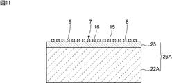
- FIG. 11 is a front sectional view of an elastic wave resonator according to a third modification of the first embodiment of the present invention.
- FIG. 12 is a front cross-sectional view of an elastic wave resonator according to a fourth modification of the first embodiment of the present invention.
- FIG. 13 is a front sectional view of an elastic wave resonator according to a fifth modification of the first embodiment of the present invention.
- FIG. 14 is a circuit diagram of a filter device according to the second embodiment of the present invention.
- FIG. 15 is a diagram showing the attenuation frequency characteristics of the filter device of the fourth comparative example.
- FIG. 16 is a diagram showing attenuation-frequency characteristics of the first band-pass filter in the fourth comparative example and the fifth comparative example.
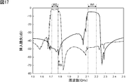
- FIG. 17 is a diagram showing the attenuation frequency characteristics of the filter device of the sixth comparative example.
- FIG. 18 is a diagram showing an attenuation frequency characteristic of the filter device according to the second embodiment of the present invention.
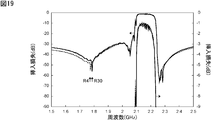
- FIG. 19 is a diagram showing the attenuation frequency characteristics of the first band-pass filter in the second embodiment of the present invention and the fourth comparative example.
- FIG. 20 is a diagram showing the return loss of the first bandpass filter in the second embodiment of the present invention and the fourth comparative example.
- FIG. 21 is a circuit diagram of a filter device according to a modification of the second embodiment of the present invention.
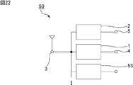
- FIG. 22 is a schematic diagram of a filter device according to the third embodiment of the present invention.
- FIG. 1 is a circuit diagram of a filter device according to a first embodiment of the present invention.
- the filter device 10 has a common connection terminal 3 and a first band-pass filter 1 and a second band-pass filter 2 commonly connected to the common connection terminal 3.
- the pass band of the second band pass filter 2 is located on the lower band side than the pass band of the first band pass filter 1.
- the common connection terminal 3 is an antenna terminal connected to the antenna.
- the filter device 10 is a duplexer, the first bandpass filter 1 is a reception filter, and the second bandpass filter 2 is a transmission filter.
- the first band-pass filter 1 and the second band-pass filter 2 may be either a reception filter or a transmission filter.
- the first band-pass filter 1 and the second band-pass filter may be used.
- Both of the pass filters 2 may be reception filters.
- the filter device 10 may be a multiplexer in which three or more band pass filters including the first band pass filter 1 and the second band pass filter 2 are connected to the common connection terminal 3.
- the first bandpass filter 1 is a ladder filter having a plurality of series arm resonators and a plurality of parallel arm resonators.
- the plurality of series arm resonators and the plurality of parallel arm resonators are all elastic wave resonators.
- the first band-pass filter 1 is connected to the common connection terminal 3 and also to the first signal terminal 4 other than the common connection terminal 3.
- the series arm resonator S1, the series arm resonator S2, the series arm resonator S3, and the series arm resonator S4 are connected in series between the common connection terminal 3 and the first signal terminal 4.
- the series arm resonator S1 is arranged closest to the common connection terminal 3 side.
- a parallel arm resonator P1 is connected between the connection point between the common connection terminal 3 and the series arm resonator S1 and the ground potential.
- the parallel arm resonator P2 is connected between the connection point between the series arm resonator S1 and the series arm resonator S2 and the ground potential.
- the parallel arm resonator P3 is connected between the ground potential and the connection point between the series arm resonator S2 and the series arm resonator S3.
- the parallel arm resonator P4 is connected between the connection point between the series arm resonator S3 and the series arm resonator S4 and the ground potential.
- the acoustic wave resonator arranged closest to the common connection terminal 3 side is the parallel arm resonator P1.
- the first band pass filter 1 has an inductor L connected in series to the ground potential side of the parallel arm resonator P1.
- the inductor L may be formed by a chip inductor, or wiring on a filter chip or wiring on a package.
- the circuit configuration of the second band pass filter 2 is not particularly limited, but in the present embodiment, the second band pass filter 2 is a ladder filter.
- the second bandpass filter 2 is connected to the common connection terminal 3 and also to the second signal terminal 5 other than the common connection terminal 3.
- a series arm resonator S101, a series arm resonator S102, a series arm resonator S103, a series arm resonator S104, and a series arm resonator S105 are arranged on a series arm connecting the common connection terminal 3 and the second signal terminal 5. ing.
- a parallel arm resonator P101, a parallel arm resonator P102, a parallel arm resonator P103, and a parallel arm resonator P104 are arranged on each parallel arm that connects the connection point between each series arm resonator and the ground potential. ..
- the second band pass filter 2 may be a longitudinally coupled resonator type elastic wave filter or the like.
- the first band-pass filter has a piezoelectric substrate 6.
- the plurality of acoustic wave resonators are formed on the piezoelectric substrate 6.
- details of the elastic wave resonator of the first band-pass filter 1 will be described.
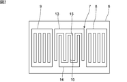
- FIG. 2 is a plan view of an elastic wave resonator of the first bandpass filter according to the first embodiment.
- the elastic wave resonator shown in FIG. 2 is the parallel arm resonator P1 arranged closest to the common connection terminal side.
- the wiring connected to the parallel arm resonator P1 is omitted.
- the parallel arm resonator P1 has a piezoelectric substrate 6 and an IDT electrode 7 provided on the piezoelectric substrate 6. By applying an AC voltage to the IDT electrode 7, elastic waves are excited. A pair of reflectors 8 and 9 are provided on both sides of the IDT electrode 7 in the elastic wave propagation direction on the piezoelectric substrate 6.
- the piezoelectric substrate 6 is a piezoelectric substrate composed of only a piezoelectric layer in this embodiment. More specifically, the piezoelectric substrate 6 is a lithium tantalate substrate. However, the piezoelectric substrate 6 may be a laminated body including a piezoelectric layer.
- the IDT electrode 7 has a first bus bar 13 and a second bus bar 14 facing each other.
- the IDT electrode 7 has a plurality of first electrode fingers 15 each having one end connected to the first bus bar 13. Further, the IDT electrode 7 has a plurality of second electrode fingers 16 each having one end connected to the second bus bar 14. The plurality of first electrode fingers 15 and the plurality of second electrode fingers 16 are interleaved with each other.
- the IDT electrode 7 may be made of a laminated metal film in which a plurality of metal layers are laminated, or may be made of a single-layer metal film.
- the reflector 8 and the reflector 9 are also made of the same material as the IDT electrode 7.
- each acoustic wave resonator other than the parallel arm resonator P1 has an IDT electrode and a reflector provided on the piezoelectric substrate 6.
- the IDT electrodes 7 in the parallel arm resonator P1 arranged closest to the common connection terminal 3 side are included.
- the electrode pitch is the smallest. More specifically, the electrode finger pitch of the IDT electrodes 7 in the parallel arm resonator P1 is smaller than the electrode finger pitch of the IDT electrodes in any other parallel arm resonator of the first bandpass filter 1.
- the electrode finger pitch is the distance between the electrode finger centers of adjacent electrode fingers.
- the inductor L is connected in series to the parallel arm resonator P1.
- the inductance of the inductor L is not particularly limited, but is 1.5 nH in the present embodiment.
- a leaky wave which is an SH type surface wave
- the filter device 10 of the present embodiment uses a leaky wave, which is a type of SH wave.
- a response of the Rayleigh wave, which is an unnecessary wave is also generated.
- the first bandpass filter 1 and the second bandpass filter 2 are configured in the same chip.
- being configured in the same chip means being configured in the same piezoelectric substrate 6.
- the first bandpass filter 1 and the second bandpass filter 2 may be formed on different substrates.
- the feature of this embodiment is that the SH wave is used, and the parallel arm resonator P1 having the smallest electrode finger pitch of the IDT electrodes among the plurality of parallel arm resonators of the first bandpass filter 1 is connected in series.
- the inductor is connected.
- the first comparative example has no inductor, and the electrode finger pitch of the IDT electrode in the parallel arm resonator arranged closest to the common connection terminal side is the same as the electrode finger pitch of the IDT electrodes in the other parallel arm resonators. Is different from the first embodiment.
- the second comparative example is the first comparative example in that the electrode finger pitch of the IDT electrodes of the parallel arm resonator arranged closest to the common connection terminal side is the same as the electrode finger pitch of the IDT electrodes of the other parallel arm resonators. Different from the embodiment.
- the third comparative example differs from the first embodiment in that it has no inductor.
- the filter device having the configuration of the first embodiment and the filter devices of the first to third comparative examples were manufactured.
- the conditions of each filter device are as follows.
- 0° ⁇ 5° in the Euler angle above is within the range of -5° or more and 5° or less.
- the inductance of the inductor in the first embodiment and the second comparative example was set to 1.5 nH.
- each elastic wave resonator of the first bandpass filter in the first embodiment and the third comparative example are as shown in Table 1 below.
- the design parameters of each acoustic wave resonator of the first bandpass filter in the first comparative example and the second comparative example are as shown in Table 2 below.
- a region where the first electrode finger and the second electrode finger overlap with each other when viewed in the elastic wave propagation direction is referred to as a crossover region.
- the dimension of the intersecting region along the direction orthogonal to the elastic wave propagation direction is defined as the intersecting width.
- the wavelengths in Table 1 and Table 2 are wavelengths defined by the electrode finger pitch of the IDT electrodes.
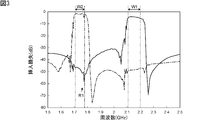
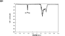
- FIG. 3 is a diagram showing an attenuation frequency characteristic of the filter device of the first comparative example.
- the solid line shows the result of the first bandpass filter, and the alternate long and short dash line shows the result of the second bandpass filter.
- An arrow R1 in FIG. 3 indicates the response of the Rayleigh wave in the first comparative example. The same applies to drawings other than FIG.
- ripples are generated in the pass band W2 of the second band pass filter. This ripple occurs at the frequency of the Rayleigh wave response indicated by arrow R1. As described above, the ripple generated in the pass band W2 of the second band pass filter is caused by the Rayleigh wave in the first band pass filter.
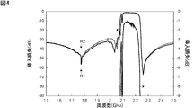
- FIG. 4 is a diagram showing attenuation-frequency characteristics of the first bandpass filter in the first comparative example and the second comparative example.
- the solid line shows the result of the second comparative example
- the broken line shows the result of the first comparative example.
- the arrow R2 indicates the response of the Rayleigh wave in the second comparative example.
- the frequency of the response due to the Rayleigh wave in the first bandpass filter does not change.
- an inductor is connected in series to the parallel arm resonator arranged closest to the common connection terminal side.
- the frequency of the attenuation pole of the second comparative example is lower than the frequency of the attenuation pole of the first comparative example.
- FIG. 5 is a diagram showing the attenuation frequency characteristics of the filter device of the third comparative example.
- the solid line shows the result of the first bandpass filter, and the alternate long and short dash line shows the result of the second bandpass filter.
- the arrow R3 indicates the response of the Rayleigh wave in the third comparative example.
- the ripple caused by the Rayleigh wave is located outside the pass band W2 of the second band pass filter.
- the electrode finger pitch of the IDT electrodes in the parallel arm resonator arranged closest to the common connection terminal side is the same as that of the first bandpass filter. It is smaller than the electrode finger pitch of the IDT electrodes in the arm resonator. Therefore, the frequency of the response due to the Rayleigh wave in the first bandpass filter shown by arrow R3 is different from that in the first comparative example.
- the insertion loss in the pass band W1 of the first band pass filter is larger than that in the first comparative example shown in FIG. More specifically, the insertion loss is ⁇ 5.4 dB in the first comparative example, and the insertion loss is ⁇ 5.6 dB in the second comparative example.
- the insertion loss in the pass band means the insertion loss having the largest absolute value in the pass band.
- the filter characteristic of the first bandpass filter is deteriorated.
- FIG. 6 is a diagram showing attenuation-frequency characteristics of the filter device according to the first embodiment.
- the solid line shows the result of the first band-pass filter
- the alternate long and short dash line shows the result of the second band-pass filter.
- the arrow R0 indicates the response of the Rayleigh wave in the first embodiment. The same applies to drawings other than FIG. 6.
- the ripple caused by the Rayleigh wave is located outside the pass band W2 of the second band pass filter.
- the electrode finger pitch of the IDT electrode in the parallel arm resonator arranged closest to the common connection terminal is the electrode finger of the IDT electrode in any other parallel arm resonator of the first band pass filter. Smaller than pitch.
- the frequency of the response due to the Rayleigh wave in the first band pass filter indicated by the arrow R0 can be made different from the frequency in the pass band W2 of the second band pass filter.
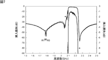
- FIG. 7 is a diagram showing attenuation-frequency characteristics of the first bandpass filter in the first embodiment and the first comparative example.
- FIG. 8 is a diagram showing the return loss of the first bandpass filter in the first embodiment and the first comparative example. 7 and 8, the solid line shows the result of the first embodiment, and the broken line shows the result of the first comparative example.
- the Rayleigh wave response occurred in the pass band W2 of the second band pass filter.
- FIGS. 7 and 8 it can be seen that the response frequency due to the Rayleigh wave is higher in the first embodiment than in the first comparative example. Therefore, as described above, the ripple caused by the Rayleigh wave can be located outside the pass band W2 of the second band pass filter.
- the insertion loss of the first bandpass filter is ⁇ 5.4 dB.
- the insertion loss of the first bandpass filter is smaller than that of the third comparative example, and is not deteriorated as compared with the first comparative example.
- the inductor is connected in series to the parallel arm resonator having the smallest electrode finger pitch of the IDT electrodes. Thereby, the deterioration of the insertion loss can be suppressed.
- the influence of the response of the Rayleigh wave on the pass band W2 of the second band pass filter is suppressed without inducing the deterioration of the filter characteristics of the first band pass filter. can do.
- the attenuation pole of the first bandpass filter is located on the higher frequency side than in the second comparative example, and It is close to the pass band W1 of the band pass filter. Thereby, deterioration of steepness in the vicinity of the end of the pass band W1 can be suppressed.
- high steepness means that the amount of change in frequency is small with respect to a certain amount of change in attenuation near the end of the pass band.
- the elastic wave resonator closest to the common connection terminal 3 is unnecessary.
- the effect of the waves is the greatest.
- the electrode finger pitch of the IDT electrodes 7 in the parallel arm resonator P1 arranged closest to the common connection terminal 3 side is the smallest.
- the inductor L is connected in series to the ground potential side of the parallel arm resonator P1.
- the inductor L may be connected in series to the parallel arm resonator having the smallest electrode finger pitch of the IDT electrodes.
- a first modified example and a second modified example of the first embodiment will be shown below.
- the pass of the second band-pass filter is brought about without deteriorating the filter characteristic of the first band-pass filter. The influence of the response due to the Rayleigh wave on the band can be suppressed.
- the inductor L is connected in series to the common connection terminal 3 side of the parallel arm resonator P1.
- the inductor L is not connected between the series arm resonator S1 and the common connection terminal 3. More specifically, between the parallel arm resonator P1 and the connection point between the common connection terminal 3 and the series arm resonator S1 to which the parallel arm resonator P1 is connected, The inductor L is connected.
- the parallel arm resonator P22 having the smallest electrode finger pitch of the IDT electrodes 7 is the second parallel arm resonator to the common connection terminal 3. Is.
- the inductor L is connected between the connection point between the series arm resonator S1 and the series arm resonator S2 and the parallel arm resonator P22.
- An inductor is not connected to the parallel arm resonator P21 arranged closest to the common connection terminal 3 side.
- the arrangement of the parallel arm resonator P22 having the smallest electrode finger pitch of the IDT electrodes 7 is not particularly limited. However, as described above, it is preferable that the parallel arm resonator P22 having the smallest electrode finger pitch of the IDT electrodes 7 is disposed on the most common connection terminal 3 side.
- the piezoelectric substrate 6 is a piezoelectric substrate composed only of a piezoelectric layer.
- the piezoelectric substrate is not limited to this, and may be a laminated body. It suffices if the filter device uses SH waves.
- third to fifth modified examples of the first embodiment will be described in which only the configuration of the piezoelectric substrate is different from that of the first embodiment. Also in the third to fifth modified examples, as in the first embodiment, the Rayleigh for the pass band of the second band pass filter is brought about without deteriorating the filter characteristic of the first band pass filter. The influence of the response due to waves can be suppressed.
- the piezoelectric substrate 26A has a high acoustic velocity material layer and a piezoelectric layer 25 provided on the high acoustic velocity material layer.
- the piezoelectric layer 25 is a lithium tantalate layer having Euler angles (0° ⁇ 5°, ⁇ , 0° ⁇ 5°) and ⁇ of ⁇ 54° to ⁇ 42°, SH waves are excited predominantly.
- the high sound velocity member layer is a layer having a relatively high sound velocity. More specifically, the acoustic velocity of the bulk wave propagating in the high acoustic velocity material layer is higher than the acoustic velocity of the elastic wave propagating in the piezoelectric layer 25.
- the high sonic velocity material layer is the high sonic velocity support substrate 22A.
- the piezoelectric layer 25 is directly provided on the high acoustic velocity support substrate 22A.
- Examples of the material of the high sonic velocity support substrate 22A include aluminum oxide, silicon carbide, silicon nitride, silicon oxynitride, silicon, sapphire, lithium tantalate, lithium niobate, quartz, alumina, zirconia, cordierite, mullite, steatite. , Forsterite, magnesia, DLC (diamond-like carbon) film, diamond, or other medium containing the above-mentioned material as a main component can be used.
- the material of the piezoelectric layer 25 is not limited to lithium tantalate.
- the material of the piezoelectric layer 25 may be, for example, lithium niobate or the like.
- the piezoelectric substrate 26A has a laminated structure in which the high acoustic velocity material layer and the piezoelectric layer 25 are laminated, the elastic wave energy can be effectively trapped on the piezoelectric layer 25 side.
- the piezoelectric substrate 26B is provided on the high sonic velocity support substrate 22A, the low sonic velocity film 24 provided on the high sonic velocity support substrate 22A, and the low sonic velocity film 24. And a piezoelectric layer 25 that is formed.
- the low sound velocity film 24 is a film having a relatively low sound velocity. More specifically, the sound velocity of the bulk wave propagating in the low acoustic velocity film 24 is lower than the sound velocity of the bulk wave propagating in the piezoelectric layer 25.
- a medium containing the above-mentioned material as a main component such as silicon oxynitride, tantalum oxide, silicon oxide, or a compound obtained by adding fluorine, carbon, or boron to silicon oxide can also be used.
- the piezoelectric substrate 26B has a laminated structure in which the high sonic velocity support substrate 22A, the low sonic velocity film 24, and the piezoelectric layer 25 are laminated in this order, the elastic wave energy is transmitted to the piezoelectric layer 25 side. Can be effectively trapped in.
- the piezoelectric substrate 26C includes a support substrate 22B, a high sonic velocity material layer provided on the support substrate 22B, and a low sonic velocity provided on the high sonic velocity material layer. It has a film 24 and a piezoelectric layer 25 provided on the low acoustic velocity film 24.
- the high sonic velocity material layer is the high sonic velocity film 23.
- the piezoelectric layer 25 is indirectly provided on the high acoustic velocity film 23 via the low acoustic velocity film 24.
- the support substrate 22B may not have a relatively high acoustic velocity.
- Examples of the material of the high sound velocity film 23 include aluminum oxide, silicon carbide, silicon nitride, silicon oxynitride, silicon, sapphire, lithium tantalate, lithium niobate, quartz, alumina, zirconia, cordierite, mullite, steatite, and the like.
- Forsterite, magnesia, DLC film or diamond, a medium containing the above-mentioned material as a main component can be used.
- Examples of the material of the support substrate 22B include aluminum oxide, lithium tantalate, lithium niobate, piezoelectric materials such as quartz, alumina, magnesia, silicon nitride, aluminum nitride, silicon carbide, zirconia, cordierite, mullite, steatite, and the like.
- Various ceramics such as forsterite, dielectrics such as sapphire, diamond and glass, semiconductors such as silicon and gallium nitride, or resins can be used.
- the piezoelectric substrate 26C has a laminated structure in which the high sonic velocity film 23, the low sonic velocity film 24, and the piezoelectric body layer 25 are laminated in this order, elastic wave energy is transmitted to the piezoelectric body layer 25 side. Can be effectively trapped.
- FIG. 14 is a circuit diagram of the filter device according to the second embodiment.
- the configuration of the first bandpass filter 31 is different from that of the first embodiment. Except for the above points, the filter device of the present embodiment has the same configuration as the filter device 10 of the first embodiment.
- the series arm resonator S31, the series arm resonator S32, and the series arm resonator S33 are provided between the common connection terminal 3 and the first signal terminal 4.
- the series arm resonator S34 and the series arm resonator S35 are connected in series with each other.
- the series arm resonator S31 is arranged closest to the common connection terminal 3 side.
- the parallel arm resonator P31 is connected between the connection point between the series arm resonator S31 and the series arm resonator S32 and the ground potential.
- the parallel arm resonator P32 is connected between the ground potential and the connection point between the series arm resonator S32 and the series arm resonator S33.
- the parallel arm resonator P33 is connected between the connection point between the series arm resonator S33 and the series arm resonator S34 and the ground potential.
- the parallel arm resonator P34 is connected between the connection point between the series arm resonator S34 and the series arm resonator S35 and the ground potential.
- the acoustic wave resonator arranged closest to the common connection terminal 3 side is the series arm resonator S31.
- the electrode finger pitch of the IDT electrodes in the series arm resonator of the first bandpass filter 31 is the smallest. More specifically, the electrode finger pitch of the IDT electrodes in the series arm resonator S31 is smaller than the electrode finger pitch of the IDT electrodes in any other series arm resonator of the first bandpass filter 31.
- the inductor L is connected in series to the common connection terminal 3 side of the series arm resonator S31.
- the inductance of the inductor L is 1.5 nH in this embodiment.
- the feature of the present embodiment is that the SH wave is used, and the common connection terminal of the series arm resonator S31 having the smallest electrode finger pitch of the IDT electrodes among the plurality of series arm resonators of the first bandpass filter 31.
- the inductor L is connected in series on the third side.
- the fourth comparative example is different from the second embodiment in that it has no inductor and the electrode finger pitch of the IDT electrode in the series arm resonator arranged closest to the common connection terminal side.
- the fifth comparative example is different from the second embodiment in the electrode finger pitch of the IDT electrodes in the series arm resonator arranged closest to the common connection terminal side.
- the sixth comparative example differs from the second embodiment in that it has no inductor.
- the filter device having the configuration of the second embodiment and the filter devices of the fourth to sixth comparative examples were manufactured.
- the conditions of each filter device are as follows.
- the inductance of the inductor in the second embodiment and the fifth comparative example was set to 1.5 nH.
- each elastic wave resonator of the first bandpass filter in the second embodiment and the sixth comparative example is as shown in Table 3 below.
- the design parameters of each acoustic wave resonator of the first bandpass filter in the fourth comparative example and the fifth comparative example are as shown in Table 4 below.
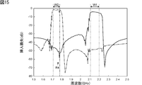
- FIG. 15 is a diagram showing an attenuation frequency characteristic of the filter device of the fourth comparative example.
- the solid line shows the result of the first bandpass filter, and the alternate long and short dash line shows the result of the second bandpass filter.
- the arrow R4 indicates the response of the Rayleigh wave in the fourth comparative example. The same applies to drawings other than FIG.
- ripples occur in the pass band W2 of the second band pass filter. This ripple occurs at the frequency of the Rayleigh wave response indicated by arrow R4. As described above, the ripple generated in the pass band W2 of the second band pass filter is caused by the Rayleigh wave in the first band pass filter.
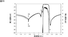
- FIG. 16 is a diagram showing the attenuation frequency characteristics of the first bandpass filter in the fourth comparative example and the fifth comparative example.
- the solid line shows the result of the fifth comparative example
- the broken line shows the result of the fourth comparative example.
- the arrow R5 indicates the response of the Rayleigh wave in the fifth comparative example.
- the frequency of the response due to the Rayleigh wave in the first bandpass filter does not change.
- the inductor is connected in series to the common connection terminal side of the series arm resonator arranged closest to the common connection terminal side.
- the response frequency due to the Rayleigh wave does not change by connecting the inductor to the series arm resonator.
- FIG. 17 is a diagram showing an attenuation frequency characteristic of the filter device of the sixth comparative example.
- the solid line shows the result of the first bandpass filter, and the alternate long and short dash line shows the result of the second bandpass filter.
- the arrow R6 indicates the response of the Rayleigh wave in the sixth comparative example.
- the ripple caused by the Rayleigh wave is located outside the pass band W2 of the second band pass filter.
- the electrode finger pitch of the IDT electrodes in the series arm resonator arranged closest to the common connection terminal side is the same as that in the first band pass filter. It is smaller than the electrode finger pitch of the IDT electrodes in the arm resonator. Therefore, the frequency of the response due to the Rayleigh wave in the first bandpass filter shown by arrow R6 is different from that in the fourth comparative example.
- the insertion loss of the first bandpass filter is larger than that of the fourth comparative example shown in FIG. More specifically, the insertion loss is ⁇ 5.4 dB in the fourth comparative example, and the insertion loss is ⁇ 5.5 dB in the sixth comparative example. As described above, in the sixth comparative example, the filter characteristics of the first bandpass filter are deteriorated.
- FIG. 18 is a diagram showing an attenuation frequency characteristic of the filter device according to the second embodiment.
- the solid line shows the result of the first bandpass filter
- the alternate long and short dash line shows the result of the second bandpass filter.
- the arrow R30 indicates the response of the Rayleigh wave in the second embodiment. The same applies to drawings other than FIG. 18.
- the ripple caused by the Rayleigh wave is located outside the pass band W2 of the second band pass filter.
- the electrode finger pitch of the IDT electrode in the series arm resonator arranged closest to the common connection terminal is the electrode finger of the IDT electrode in any other series arm resonator of the first band pass filter. Smaller than pitch.
- the frequency of the response due to the Rayleigh wave in the first band pass filter shown by arrow R30 can be made different from the frequency in the pass band W2 of the second band pass filter.
- the electrode finger pitch of the IDT electrodes in the series arm resonators other than the series arm resonator arranged closest to the common connection terminal may be the smallest.
- FIG. 19 is a diagram showing attenuation-frequency characteristics of the first bandpass filter in the second embodiment and the fourth comparative example.
- FIG. 20 is a diagram showing the return loss of the first bandpass filter in the second embodiment and the fourth comparative example. 19 and 20, the solid line shows the result of the second embodiment, and the broken line shows the result of the fourth comparative example.
- the Rayleigh wave response occurred in the pass band W2 of the second band pass filter.
- the response frequency due to the Rayleigh wave is higher than that in the fourth comparative example. Therefore, as described above, the ripple caused by the Rayleigh wave can be located outside the pass band W2 of the second band pass filter.
- the insertion loss in the pass band W1 of the first band pass filter is ⁇ 5.1 dB.
- the insertion loss in the pass band W1 of the first band pass filter is smaller than that in the sixth comparative example and the fourth comparative example.
- the inductor is connected in series to the common connection terminal side of the series arm resonator having the smallest electrode finger pitch of the IDT electrodes. Thereby, the deterioration of the insertion loss in the pass band W1 can be suppressed.
- the influence of the response of the Rayleigh wave on the pass band W2 of the second band pass filter is suppressed without inducing the deterioration of the filter characteristics of the first band pass filter. can do.
- the electrode finger pitch of the IDT electrodes 7 in the series arm resonator S31 arranged closest to the common connection terminal 3 side is the smallest. .. Thereby, the influence of the response due to the Rayleigh wave on the second band pass filter 2 can be further suppressed.
- the inductor L may be connected in series to the common connection terminal side of the series arm resonator having the smallest IDT electrode electrode pitch.
- a modified example of the second embodiment will be shown below.
- the series arm resonator S42 having the smallest electrode finger pitch of the IDT electrodes is the second series arm resonator closest to the common connection terminal 3.
- the inductor L is connected in series to the common connection terminal 3 side of the series arm resonator S42. More specifically, between the series arm resonator S42 and the connection point between the series arm resonator S41 and the series arm resonator S42 to which the parallel arm resonator P31 is connected. , Inductor L is connected.
- the arrangement of the series arm resonator S42 having the smallest electrode finger pitch of the IDT electrodes 7 is not particularly limited. However, as described above, it is preferable that the series arm resonator S42 having the smallest electrode finger pitch of the IDT electrodes is disposed on the most common connection terminal 3 side.
- the response by the Rayleigh wave to the pass band of the second band pass filter 2 is caused without deteriorating the filter characteristic of the first band pass filter 41. The influence of can be suppressed.
- FIG. 22 is a schematic diagram of the filter device according to the third embodiment.
- the filter device 50 of the third embodiment is a multiplexer in which three or more band pass filters are commonly connected to the common connection terminal 3. More specifically, the filter device 50 includes a first band-pass filter 1, a second band-pass filter 2, and a third band-pass filter 53, which are commonly connected to the common connection terminal 3. Have.
- the first bandpass filter 1 and the second bandpass filter 2 have the same configurations as the first bandpass filter 1 and the second bandpass filter 2 in the first embodiment.
- the circuit configuration of the third bandpass filter 53 is not particularly limited.
- the filter device 50 has a first band-pass filter and a second band-pass filter similar to those of the first embodiment, the second embodiment, or each of these modifications. It should be.
- the number of band-pass filters commonly connected to the common connection terminal 3 is not particularly limited.
- a band-pass filter other than the first band-pass filter 1, the second band-pass filter 2 and the third band-pass filter 53 is also connected to the common connection terminal 3 of the filter device 50 of the present embodiment. ing.
- the filter device 50 of this embodiment has a first band-pass filter 1 and a second band-pass filter 2 similar to those of the first embodiment. Therefore, similarly to the first embodiment, the influence of the response due to the Rayleigh wave on the pass band of the second band pass filter 2 is suppressed without deteriorating the filter characteristic of the first band pass filter 1. can do.
Landscapes
- Physics & Mathematics (AREA)
- Acoustics & Sound (AREA)
- Surface Acoustic Wave Elements And Circuit Networks Thereof (AREA)
Abstract
Description
第1の帯域通過型フィルタの通過帯域…2110MHz~2200MHz
第2の帯域通過型フィルタの通過帯域…1710MHz~1780MHz
圧電性基板の材料…タンタル酸リチウム(LiTaO3)
圧電性基板のオイラー角…(0°±5°,θ,0°±5°)、θ -54°~-42°


第1の帯域通過型フィルタの通過帯域…2110MHz~2200MHz
第2の帯域通過型フィルタの通過帯域…1710MHz~1780MHz
圧電性基板の材料…タンタル酸リチウム(LiTaO3)
圧電性基板のオイラー角…(0°±5°,θ,0°±5°)、θ -54°~-42°


2…第2の帯域通過型フィルタ
3…共通接続端子
4…第1の信号端子
5…第2の信号端子
6…圧電性基板
7…IDT電極
8…反射器
9…反射器
10…フィルタ装置
13…第1のバスバー
14…第2のバスバー
15…第1の電極指
16…第2の電極指
21A,21B…第1の帯域通過型フィルタ
22A…高音速支持基板
22B…支持基板
23…高音速膜
24…低音速膜
25…圧電体層
26A~26C…圧電性基板
31,41…第1の帯域通過型フィルタ
50…フィルタ装置
53…第3の帯域通過型フィルタ
L…インダクタ
P1~P3、P21,P22,P31~P34,P101~P104…並列腕共振子
S1~S4、S31~S35,S41,S42,S101~S105…直列腕共振子
Claims (14)
- 共通接続端子と、
前記共通接続端子に接続されており、圧電性基板と、前記圧電性基板上において構成されている複数の弾性波共振子と、インダクタと、を有する第1の帯域通過型フィルタと、
前記共通接続端子に接続されており、通過帯域が前記第1の帯域通過型フィルタの通過帯域よりも低域側に位置する第2の帯域通過型フィルタと、
を備え、
SH波を利用しており、
前記第1の帯域通過型フィルタが直列腕共振子及び複数の並列腕共振子を有するラダー型フィルタであり、前記直列腕共振子及び前記複数の並列腕共振子が、それぞれIDT電極を有する弾性波共振子であり、
前記第1の帯域通過型フィルタの前記複数の並列腕共振子のうち前記IDT電極の電極指ピッチが最も小さい並列腕共振子に、直列に前記インダクタが接続されている、フィルタ装置。 - 共通接続端子と、
前記共通接続端子に接続されており、圧電性基板と、前記圧電性基板上において構成されている複数の弾性波共振子と、インダクタと、を有する第1の帯域通過型フィルタと、
前記共通接続端子に接続されており、通過帯域が前記第1の帯域通過型フィルタの通過帯域よりも低域側に位置する第2の帯域通過型フィルタと、
を備え、
前記圧電性基板は、オイラー角(φ,θ,ψ)におけるθが-54°~-42°であるタンタル酸リチウム層を有し、
前記第1の帯域通過型フィルタが直列腕共振子及び複数の並列腕共振子を有するラダー型フィルタであり、前記直列腕共振子及び前記複数の並列腕共振子が、それぞれIDT電極を有する弾性波共振子であり、
前記第1の帯域通過型フィルタの前記複数の並列腕共振子のうち前記IDT電極の電極指ピッチが最も小さい並列腕共振子に、直列に前記インダクタが接続されている、フィルタ装置。 - 共通接続端子と、
前記共通接続端子に接続されており、圧電性基板と、前記圧電性基板上において構成されている複数の弾性波共振子と、インダクタと、を有する第1の帯域通過型フィルタと、
前記共通接続端子に接続されており、通過帯域が前記第1の帯域通過型フィルタの通過帯域よりも低域側に位置する第2の帯域通過型フィルタと、
を備え、
SH波を利用しており、
前記第1の帯域通過型フィルタが並列腕共振子及び複数の直列腕共振子を有するラダー型フィルタであり、前記複数の直列腕共振子及び前記並列腕共振子が、それぞれIDT電極を有する弾性波共振子であり、
前記第1の帯域通過型フィルタの前記複数の直列腕共振子のうち前記IDT電極の電極指ピッチが最も小さい直列腕共振子の前記共通接続端子側に、直列に前記インダクタが接続されている、フィルタ装置。 - 共通接続端子と、
前記共通接続端子に接続されており、圧電性基板と、前記圧電性基板上において構成されている複数の弾性波共振子と、インダクタと、を有する第1の帯域通過型フィルタと、
前記共通接続端子に接続されており、通過帯域が前記第1の帯域通過型フィルタの通過帯域よりも低域側に位置する第2の帯域通過型フィルタと、
を備え、
前記圧電性基板は、オイラー角(φ,θ,ψ)におけるθが-54°~-42°であるタンタル酸リチウム層を有し、
前記第1の帯域通過型フィルタが並列腕共振子及び複数の直列腕共振子を有するラダー型フィルタであり、前記複数の直列腕共振子及び前記並列腕共振子が、それぞれIDT電極を有する弾性波共振子であり、
前記第1の帯域通過型フィルタの前記複数の直列腕共振子のうち前記IDT電極の電極指ピッチが最も小さい直列腕共振子の前記共通接続端子側に、直列に前記インダクタが接続されている、フィルタ装置。 - 前記IDT電極の電極指ピッチが最も小さい前記並列腕共振子の前記共通接続端子側に、直列に前記インダクタが接続されている、請求項1または2に記載のフィルタ装置。
- 前記IDT電極の電極指ピッチが最も小さい前記並列腕共振子のグラウンド電位側に、直列に前記インダクタが接続されている、請求項1または2に記載のフィルタ装置。
- 前記IDT電極の電極指ピッチが最も小さい前記並列腕共振子が、前記複数の弾性波共振子のうち最も前記共通接続端子側に配置されている、請求項1、2、5または6のいずれか1項に記載のフィルタ装置。
- 前記IDT電極の電極指ピッチが最も小さい前記直列腕共振子が、前記複数の弾性波共振子のうち最も前記共通接続端子側に配置されている、請求項3または4に記載のフィルタ装置。
- 前記圧電性基板がタンタル酸リチウム基板である、請求項1~8のいずれか1項に記載のフィルタ装置。
- 前記圧電性基板が、高音速材料層と、前記高音速材料層上に直接的または間接的に設けられている圧電体層と、を有し、
前記高音速材料層を伝搬するバルク波の音速が、前記圧電体層を伝搬する弾性波の音速よりも高い、請求項1~8のいずれか1項に記載のフィルタ装置。 - 前記高音速材料層が高音速支持基板である、請求項10に記載のフィルタ装置。
- 前記圧電性基板が支持基板をさらに有し、
前記高音速材料層が、前記支持基板と前記圧電体層との間に設けられている高音速膜である、請求項10に記載のフィルタ装置。 - 前記圧電性基板が、前記高音速材料層と前記圧電体層との間に設けられている低音速膜をさらに有し、
前記低音速膜を伝搬するバルク波の音速が、前記圧電体層を伝搬するバルク波の音速よりも低い、請求項10~12のいずれか1項に記載のフィルタ装置。 - 前記共通接続端子に、前記第1の帯域通過型フィルタ及び前記第2の帯域通過型フィルタと共通接続された少なくとも1つの帯域通過型フィルタをさらに備える、請求項1~13のいずれか1項に記載のフィルタ装置。
Priority Applications (4)
| Application Number | Priority Date | Filing Date | Title |
|---|---|---|---|
| KR1020217014430A KR102587886B1 (ko) | 2018-12-25 | 2019-11-19 | 필터 장치 |
| CN201980085485.XA CN113228509B (zh) | 2018-12-25 | 2019-11-19 | 滤波器装置 |
| JP2020562923A JP6940012B2 (ja) | 2018-12-25 | 2019-11-19 | フィルタ装置 |
| US17/322,983 US11831301B2 (en) | 2018-12-25 | 2021-05-18 | Filter device |
Applications Claiming Priority (2)
| Application Number | Priority Date | Filing Date | Title |
|---|---|---|---|
| JP2018-241300 | 2018-12-25 | ||
| JP2018241300 | 2018-12-25 |
Related Child Applications (1)
| Application Number | Title | Priority Date | Filing Date |
|---|---|---|---|
| US17/322,983 Continuation US11831301B2 (en) | 2018-12-25 | 2021-05-18 | Filter device |
Publications (1)
| Publication Number | Publication Date |
|---|---|
| WO2020137263A1 true WO2020137263A1 (ja) | 2020-07-02 |
Family
ID=71129731
Family Applications (1)
| Application Number | Title | Priority Date | Filing Date |
|---|---|---|---|
| PCT/JP2019/045254 WO2020137263A1 (ja) | 2018-12-25 | 2019-11-19 | フィルタ装置 |
Country Status (5)
| Country | Link |
|---|---|
| US (1) | US11831301B2 (ja) |
| JP (1) | JP6940012B2 (ja) |
| KR (1) | KR102587886B1 (ja) |
| CN (1) | CN113228509B (ja) |
| WO (1) | WO2020137263A1 (ja) |
Cited By (1)
| Publication number | Priority date | Publication date | Assignee | Title |
|---|---|---|---|---|
| WO2023090238A1 (ja) * | 2021-11-17 | 2023-05-25 | 株式会社村田製作所 | マルチプレクサ |
Families Citing this family (1)
| Publication number | Priority date | Publication date | Assignee | Title |
|---|---|---|---|---|
| CN113708739A (zh) * | 2021-08-27 | 2021-11-26 | 中国科学院上海微系统与信息技术研究所 | 一种声波滤波器 |
Citations (5)
| Publication number | Priority date | Publication date | Assignee | Title |
|---|---|---|---|---|
| JP2008160562A (ja) * | 2006-12-25 | 2008-07-10 | Kyocera Corp | 分波器および通信装置 |
| JP2015073331A (ja) * | 2010-12-24 | 2015-04-16 | 株式会社村田製作所 | 弾性波装置 |
| JP2015092782A (ja) * | 2011-09-30 | 2015-05-14 | 株式会社村田製作所 | 弾性波装置 |
| WO2017038679A1 (ja) * | 2015-08-31 | 2017-03-09 | 京セラ株式会社 | 弾性表面波素子 |
| WO2018139598A1 (ja) * | 2017-01-30 | 2018-08-02 | 京セラ株式会社 | 弾性波フィルタ、分波器および通信装置 |
Family Cites Families (7)
| Publication number | Priority date | Publication date | Assignee | Title |
|---|---|---|---|---|
| JP2008205893A (ja) * | 2007-02-21 | 2008-09-04 | Ngk Insulators Ltd | デュプレクサ |
| CN103004085B (zh) * | 2011-06-23 | 2015-04-15 | 天工松下滤波方案日本有限公司 | 梯型弹性波滤波器及使用该弹性波滤波器的天线双工器 |
| JP2013081068A (ja) | 2011-10-04 | 2013-05-02 | Hitachi Media Electoronics Co Ltd | ワンチップ漏洩表面弾性波装置 |
| CN105474541B (zh) * | 2013-08-21 | 2018-01-12 | 株式会社村田制作所 | 可调谐滤波器 |
| CN107636961B (zh) * | 2015-06-22 | 2021-02-23 | 株式会社村田制作所 | 弹性波滤波器装置 |
| US10056879B2 (en) * | 2016-04-21 | 2018-08-21 | Murata Manufacturing Co., Ltd. | Elastic wave filter device |
| CN110383683B (zh) * | 2017-03-09 | 2023-04-28 | 株式会社村田制作所 | 多工器、高频前端电路以及通信装置 |
-
2019
- 2019-11-19 WO PCT/JP2019/045254 patent/WO2020137263A1/ja active Application Filing
- 2019-11-19 JP JP2020562923A patent/JP6940012B2/ja active Active
- 2019-11-19 CN CN201980085485.XA patent/CN113228509B/zh active Active
- 2019-11-19 KR KR1020217014430A patent/KR102587886B1/ko active IP Right Grant
-
2021
- 2021-05-18 US US17/322,983 patent/US11831301B2/en active Active
Patent Citations (5)
| Publication number | Priority date | Publication date | Assignee | Title |
|---|---|---|---|---|
| JP2008160562A (ja) * | 2006-12-25 | 2008-07-10 | Kyocera Corp | 分波器および通信装置 |
| JP2015073331A (ja) * | 2010-12-24 | 2015-04-16 | 株式会社村田製作所 | 弾性波装置 |
| JP2015092782A (ja) * | 2011-09-30 | 2015-05-14 | 株式会社村田製作所 | 弾性波装置 |
| WO2017038679A1 (ja) * | 2015-08-31 | 2017-03-09 | 京セラ株式会社 | 弾性表面波素子 |
| WO2018139598A1 (ja) * | 2017-01-30 | 2018-08-02 | 京セラ株式会社 | 弾性波フィルタ、分波器および通信装置 |
Cited By (1)
| Publication number | Priority date | Publication date | Assignee | Title |
|---|---|---|---|---|
| WO2023090238A1 (ja) * | 2021-11-17 | 2023-05-25 | 株式会社村田製作所 | マルチプレクサ |
Also Published As
| Publication number | Publication date |
|---|---|
| KR102587886B1 (ko) | 2023-10-10 |
| US20210273633A1 (en) | 2021-09-02 |
| KR20210072090A (ko) | 2021-06-16 |
| US11831301B2 (en) | 2023-11-28 |
| CN113228509A (zh) | 2021-08-06 |
| JP6940012B2 (ja) | 2021-09-22 |
| JPWO2020137263A1 (ja) | 2021-09-27 |
| CN113228509B (zh) | 2024-04-16 |
Similar Documents
| Publication | Publication Date | Title |
|---|---|---|
| US10476470B2 (en) | Elastic wave filter device | |
| CN107710614B (zh) | 弹性波滤波器、多工器、双工器、高频前端电路以及通信装置 | |
| WO2018168836A1 (ja) | 弾性波素子、弾性波フィルタ装置およびマルチプレクサ | |
| JP2019036856A (ja) | マルチプレクサ | |
| US10958241B2 (en) | Extractor | |
| CN111527699B (zh) | 弹性波滤波器 | |
| WO2018092511A1 (ja) | 弾性表面波フィルタおよびマルチプレクサ | |
| WO2021002321A1 (ja) | 弾性波フィルタおよびマルチプレクサ | |
| KR20190049761A (ko) | 탄성파 필터 장치 | |
| WO2020137263A1 (ja) | フィルタ装置 | |
| JP6658867B2 (ja) | 複合フィルタ装置 | |
| WO2020044979A1 (ja) | フィルタ装置およびマルチプレクサ | |
| WO2020036100A1 (ja) | 弾性波フィルタ | |
| JP2019004364A (ja) | 弾性波フィルタ及びマルチプレクサ | |
| CN110809858B (zh) | 多工器 | |
| CN113056874A (zh) | 提取器 | |
| WO2023002909A1 (ja) | 複合フィルタ装置 | |
| WO2023054301A1 (ja) | 弾性波フィルタ装置およびマルチプレクサ | |
| CN217183269U (zh) | 弹性波滤波器装置 | |
| CN112688662B (zh) | 滤波器装置以及多工器 | |
| WO2023074373A1 (ja) | 弾性波共振子、弾性波フィルタ装置およびマルチプレクサ | |
| WO2023282328A1 (ja) | 弾性波素子、弾性波フィルタ装置およびマルチプレクサ | |
| WO2022019169A1 (ja) | ラダー型フィルタ | |
| JP2023044392A (ja) | 弾性波素子、弾性波フィルタ装置およびマルチプレクサ | |
| KR20220035948A (ko) | 탄성파 장치, 필터 장치 및 멀티플렉서 |
Legal Events
| Date | Code | Title | Description |
|---|---|---|---|
| 121 | Ep: the epo has been informed by wipo that ep was designated in this application |
Ref document number: 19904808 Country of ref document: EP Kind code of ref document: A1 |
|
| ENP | Entry into the national phase |
Ref document number: 20217014430 Country of ref document: KR Kind code of ref document: A |
|
| ENP | Entry into the national phase |
Ref document number: 2020562923 Country of ref document: JP Kind code of ref document: A |
|
| NENP | Non-entry into the national phase |
Ref country code: DE |
|
| 122 | Ep: pct application non-entry in european phase |
Ref document number: 19904808 Country of ref document: EP Kind code of ref document: A1 |