WO2020129664A1 - 光導波路とその製造方法 - Google Patents
光導波路とその製造方法 Download PDFInfo
- Publication number
- WO2020129664A1 WO2020129664A1 PCT/JP2019/047564 JP2019047564W WO2020129664A1 WO 2020129664 A1 WO2020129664 A1 WO 2020129664A1 JP 2019047564 W JP2019047564 W JP 2019047564W WO 2020129664 A1 WO2020129664 A1 WO 2020129664A1
- Authority
- WO
- WIPO (PCT)
- Prior art keywords
- layer
- optical waveguide
- etch stop
- core layer
- core
- Prior art date
- Legal status (The legal status is an assumption and is not a legal conclusion. Google has not performed a legal analysis and makes no representation as to the accuracy of the status listed.)
- Ceased
Links
Images

Classifications
-
- G—PHYSICS
- G02—OPTICS
- G02B—OPTICAL ELEMENTS, SYSTEMS OR APPARATUS
- G02B6/00—Light guides; Structural details of arrangements comprising light guides and other optical elements, e.g. couplings
- G02B6/10—Light guides; Structural details of arrangements comprising light guides and other optical elements, e.g. couplings of the optical waveguide type
- G02B6/12—Light guides; Structural details of arrangements comprising light guides and other optical elements, e.g. couplings of the optical waveguide type of the integrated circuit kind
- G02B6/122—Basic optical elements, e.g. light-guiding paths
-
- G—PHYSICS
- G02—OPTICS
- G02B—OPTICAL ELEMENTS, SYSTEMS OR APPARATUS
- G02B6/00—Light guides; Structural details of arrangements comprising light guides and other optical elements, e.g. couplings
- G02B6/10—Light guides; Structural details of arrangements comprising light guides and other optical elements, e.g. couplings of the optical waveguide type
- G02B6/12—Light guides; Structural details of arrangements comprising light guides and other optical elements, e.g. couplings of the optical waveguide type of the integrated circuit kind
- G02B6/12004—Combinations of two or more optical elements
-
- G—PHYSICS
- G02—OPTICS
- G02B—OPTICAL ELEMENTS, SYSTEMS OR APPARATUS
- G02B6/00—Light guides; Structural details of arrangements comprising light guides and other optical elements, e.g. couplings
- G02B6/10—Light guides; Structural details of arrangements comprising light guides and other optical elements, e.g. couplings of the optical waveguide type
- G02B6/12—Light guides; Structural details of arrangements comprising light guides and other optical elements, e.g. couplings of the optical waveguide type of the integrated circuit kind
- G02B6/13—Integrated optical circuits characterised by the manufacturing method
- G02B6/132—Integrated optical circuits characterised by the manufacturing method by deposition of thin films
-
- G—PHYSICS
- G02—OPTICS
- G02B—OPTICAL ELEMENTS, SYSTEMS OR APPARATUS
- G02B6/00—Light guides; Structural details of arrangements comprising light guides and other optical elements, e.g. couplings
- G02B6/10—Light guides; Structural details of arrangements comprising light guides and other optical elements, e.g. couplings of the optical waveguide type
- G02B6/12—Light guides; Structural details of arrangements comprising light guides and other optical elements, e.g. couplings of the optical waveguide type of the integrated circuit kind
- G02B6/13—Integrated optical circuits characterised by the manufacturing method
- G02B6/136—Integrated optical circuits characterised by the manufacturing method by etching
-
- G—PHYSICS
- G02—OPTICS
- G02B—OPTICAL ELEMENTS, SYSTEMS OR APPARATUS
- G02B6/00—Light guides; Structural details of arrangements comprising light guides and other optical elements, e.g. couplings
- G02B6/10—Light guides; Structural details of arrangements comprising light guides and other optical elements, e.g. couplings of the optical waveguide type
- G02B6/12—Light guides; Structural details of arrangements comprising light guides and other optical elements, e.g. couplings of the optical waveguide type of the integrated circuit kind
- G02B2006/12133—Functions
- G02B2006/12138—Sensor
Definitions
- the present invention relates to an optical waveguide and a manufacturing method thereof.
- the present invention relates to an optical waveguide that suppresses the core layer of the optical waveguide from sinking into the lower clad layer due to the heat treatment of the manufacturing process, and makes it possible to reduce the loss of the visible light waveguide, and a manufacturing method thereof.
- the present invention relates to an optical waveguide and a manufacturing method thereof.
- a planar lightwave circuit (PLC, hereinafter referred to as a silica-based PLC) made of a silica-based glass material is mainly used in an optical communication/optical signal processing system.
- Silica-based waveguides constituting the silica-based PLC is designed and prepared for communication wavelength, Its core material, SiO 2 -GeO 2 is used which is doped with GeO 2 in SiO 2.
- SiO 2 —GeO 2 is used as the core material of the silica-based waveguide, it is possible to manufacture a proven optical waveguide with a very low loss without a large absorption loss in the communication wavelength band.
- silica-based PLC devices have been used not only in optical communication/optical signal processing systems, but also as image/sensor devices, and silica-based PLC devices designed for visible light wavelengths have also been developed.
- SiO 2 —GeO 2 used as the core material of the silica-based waveguide has no absorption in the communication wavelength band, but has absorption in the visible light wavelength band. Therefore, visible light is input to the silica-based PLC device. There is a problem that optical characteristics are deteriorated due to light absorption caused by electronic excitation when propagating through the waveguide.
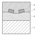
- FIG. 1 shows a conventional optical waveguide structure having a cladding layer made of silica glass doped with boron or fluorine.
- FIG. 1 shows a Si substrate 1, a SiO 2 lower clad layer 2 formed on the Si substrate 1, a pure quartz glass core layer 3 formed on the SiO 2 lower clad layer 2, and a pure quartz glass core layer.
- 3 shows an optical waveguide structure including a SiO 2 lower clad layer 2 and a SiO 2 upper clad layer 4 formed on the pure silica glass core layer 3 so as to be embedded therein.
- the SiO 2 lower clad layer 2 and the SiO 2 upper clad layer 4 are doped with boron or fluorine.
- the softening point of SiO 2 becomes lower as the amount of the dopant increases, when such a silica glass doped with boron or fluorine is used as the cladding layer, the cladding layer is softened at a temperature lower than that of the pure silica glass core layer 3. Will be done. Therefore, when a heat treatment such as a flame deposition method is performed in order to stabilize the quality of the core film and flatten the cladding layer in the process of manufacturing the optical waveguide, as shown in FIG. 1, the pure silica glass core layer having a high softening point is obtained. 3 is sunk into the SiO 2 lower clad layer 2 which is rich in dopant and has a low softening point.
- the softening point means a temperature at which the solid material is softened and begins to deform when the solid material is heated.
- pure quartz glass has a value of about 1600° C.
- SiO 2 clad layer having a low point the value is about 900°C.
- FIG. 2 shows a conventional optical waveguide structure shown in Patent Document 2.
- the structure is shown.
- the SiO 2 lower clad layer 12 and the SiO 2 upper clad layer 14 are doped with boron or fluorine as in FIG.
- the thickness is reduced by controlling the thickness of the core film 15 left when the pure silica glass core layer 13 is etched.
- the etching rate varies in the plane of the substrate, the remaining thickness of the core film 15 varies in the plane, which causes a problem of lowering the yield.
- the present invention has been made in view of the above-mentioned problems, and suppresses the core layer from sinking into the lower cladding layer during heat treatment, which enables a loss reduction of the visible light waveguide and reduces the etching rate. It is an object of the present invention to provide an optical waveguide capable of suppressing a decrease in yield due to variations within a substrate surface.
- one aspect of the optical waveguide of the present invention is characterized in that a thin etch stop layer formed of a material different from that of the core layer is provided below the core layer.
- (Structure 1) Board A lower clad layer formed on the substrate, An etch stop layer formed on the lower clad layer, A core layer formed on the etch stop layer, An optical waveguide comprising an upper clad layer formed on the core layer and the etch stop layer, The optical waveguide, wherein the etch stop layer is made of a material having an etching rate lower than that of the material forming the core layer and having a softening point higher than that of the material forming the core layer.
- (Structure 2) The optical waveguide according to structure 1, wherein the thickness of the etch stop layer is 2% or less of that of the core layer.
- the etch stop layer is made of a material containing aluminum oxide (Al 2 O 3 ), magnesium oxide (MgO), yttrium oxide (Y 2 O 3 ), and yttrium aluminum garnet (YAG). 3.
- Al 2 O 3 aluminum oxide
- MgO magnesium oxide
- Y 2 O 3 yttrium oxide
- YAG yttrium aluminum garnet
- (Structure 6) Forming a lower clad layer on the substrate, Forming an etch stop layer on the lower cladding layer, Forming a core layer on the etch stop layer;
- a step of forming an upper clad layer on the core layer and the etch stop layer, and a method of manufacturing an optical waveguide comprising: The method of manufacturing an optical waveguide, wherein the etch stop layer is formed of a material having an etching rate lower than that of the material forming the core layer and having a higher softening point than the material forming the core layer. ..
- (Structure 7) The method for manufacturing an optical waveguide according to the constitution 6, wherein the thickness of the etch stop layer is 2% or less of that of the core layer.
- the etch stop layer is formed of a material including aluminum oxide (Al 2 O 3 ), magnesium oxide (MgO), yttrium oxide (Y 2 O 3 ), and yttrium aluminum garnet (YAG).
- Al 2 O 3 aluminum oxide
- MgO magnesium oxide
- Y 2 O 3 yttrium oxide
- YAG yttrium aluminum garnet
- the present invention it is possible to suppress the core layer from sinking into the lower clad layer during the heat treatment of the manufacturing process, to reduce the loss of the visible light waveguide, and to achieve the microloading effect. It is possible to provide an optical waveguide that suppresses the in-plane variation of the waveguide shape due to the in-plane distribution of the etching rate.
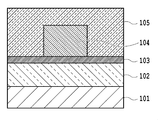
- FIG. 3 is a substrate cross-sectional view showing the optical waveguide structure according to the embodiment of the present invention.
- a substrate 101 made of, for example, Si
- a lower clad layer 102 formed on the substrate 101 for example, silica glass
- a lower clad layer 102 formed on the lower clad layer 102 for example, aluminum oxide (Al 2 O 3 )
- an etch stop layer 103 for example, a core layer 104 formed on the etch stop layer 103, for example, pure silica glass, and a core layer 104 formed on the core layer 104, for example, silica glass.
- An optical waveguide structure comprising the configured upper cladding layer 105 is shown.
- the lower clad 102 and the upper clad layer 105 are made of, for example, silica-based glass doped with fluorine so that the relative refractive index difference ⁇ is about 2% as compared with the material forming the core layer 104.
- the etch stop layer 103 has a sufficient thickness to float the core layer 104 due to surface tension, and the peak of the electric field intensity distribution in the waveguide cross-section inward direction (for example, the vertical direction in the figure) of the propagating light propagating in the optical waveguide. However, it is desirable to be thin so as not to move from the core layer 104 to the etch stop layer 103. For example, the thickness may be 2% or less of the thickness of the core layer 104.
- the lower limit of the etch stop layer is determined by the film thickness controllability during deposition, and is about 0.01 ⁇ m.
- a lower cladding layer 102 is formed by depositing 20 ⁇ m of fluorine-doped SiO 2 on a substrate 101 having a thickness of 1 mm and made of, for example, Si by using, for example, a flame deposition method.
- etch stop layer 103 aluminum oxide is deposited by 0.02 ⁇ m to form the etch stop layer 103 by using, for example, ALD (Atomic Layer Deposition) method.
- ALD Atomic Layer Deposition
- a pure quartz glass film is deposited on the etch stop layer 103 to a thickness of 1 ⁇ m by using, for example, a sputtering method. This pure quartz glass film is etched into a rectangular substrate cross section with a desired optical circuit pattern to form a core layer 104.
- SiO 2 doped with fluorine so as to have a refractive index equivalent to that of the lower clad layer 102 was deposited to 20 ⁇ m to form an upper clad layer 105.
- the etching amount of the pure quartz glass film is kept constant. Therefore, the in-plane variation of the shape of the core layer 104 due to the microloading effect and the in-plane distribution of the etching rate can be suppressed. Further, since the softening point of aluminum oxide, which is the etch stop layer, is higher than that of the silica-based glass, it does not soften during the heat treatment, and the core layer 104 can be floated by the surface tension and the subsidence to the lower cladding 102 can be suppressed. It will be possible.
- the lower clad layer 102 and the upper clad layer 105 are deposited by the flame deposition method, and the core layer 104 is deposited by the sputtering method.
- the deposition methods are the flame deposition method, the chemical vapor deposition method, and the sputtering method. You can freely choose from.
- the substrate 101 is made of Si in the above-mentioned embodiment, it is preferably made of any material as long as it has a melting point of 1400° C. or higher and a thermal expansion coefficient of 0.5 ⁇ 10 ⁇ 6 /° C. or higher. Good.
- the lower clad layer 102 and the upper clad layer 105 are made of SiO 2 doped with fluorine, but boron, fluorine, or both may be used as the dopant.
- the relative refractive index difference ⁇ does not have to be 2%.
- the etch stop layer 103 is made of aluminum oxide (Al 2 O 3 ), but, for example, magnesium oxide (MgO), yttrium oxide (Y 2 O 3 ), yttrium aluminum garnet (YAG). ) May be included.
- the material and the thickness of the etch stop layer 103 are such that the etching rate is lower than that of the core layer 104 with respect to the etching gas used for forming the core layer 104 of the waveguide, and the softening point or melting point of the core layer 104 is higher than that of the core layer 104. , And a film thickness that allows the core layer 104 to float due to surface tension.
- the upper clad layer 105 has the same refractive index as that of the lower clad layer 102, but if the refractive index is lower than that of the core layer 104, the upper clad layer 102 and the upper clad layer 102 are The cladding layer 105 may have a different refractive index. Further, the lower clad layer 102 and the upper clad layer 105 may be the same or different.
- the present invention it is possible to suppress the core layer from sinking into the lower clad layer during the heat treatment of the manufacturing process, to reduce the loss of the visible light waveguide, and to suppress the in-plane variation of the optical waveguide shape. It is possible to provide the optical waveguide.
Landscapes
- Physics & Mathematics (AREA)
- Engineering & Computer Science (AREA)
- Microelectronics & Electronic Packaging (AREA)
- General Physics & Mathematics (AREA)
- Optics & Photonics (AREA)
- Optical Integrated Circuits (AREA)
Abstract
製造プロセスの熱処理においてコア層が下部クラッド層中に沈み込むことを抑制して可視光用導波路の低損失化を可能にするとともに、光導波路形状の基板面内ばらつきを抑制する光導波路を提供する。基板と、前記基板上に形成された下部クラッド層と、前記下部クラッド層上に形成されたエッチストップ層と、前記エッチストップ層上に形成されたコア層と、前記コア層及び前記エッチストップ層上に形成された上部クラッド層と、を備えた光導波路であって、前記エッチストップ層はコア層を構成する材料よりもエッチング速度が小さく、且つ前記コア層を構成する材料と比較して軟化点が高い材料で構成されていることを特徴とする光導波路とした。
Description
本発明は、光導波路とその製造方法に関する。特に製造プロセスの熱処理によって光導波路のコア層が下部クラッド層へ沈み込むことを抑制して、可視光用導波路の低損失化を可能にする光導波路とその製造方法に関する。それとともに、マイクロローディング効果やエッチング量の基板面内における分布に起因する、可視光用導波路の形状の基板面内ばらつきを抑制して、導波路構造の基板面内における均質化を実現可能な光導波路及びその製造方法に関する。
従来、石英系ガラス材料によって構成された平面光波回路(Planar Lightwave Circuits:PLC 以下、石英系PLC)は、光通信・光信号処理システムを中心に用いられている。石英系PLCを構成する石英系導波路は、通信波長用に設計・作製されており、そのコア材料には、SiO2にGeO2をドープしたSiO2-GeO2が用いられている。(例えば特許文献1参照)。石英系導波路のコア材料としてSiO2-GeO2を用いた場合、通信波長帯では、大きな吸収損失もなく、極めて低損失で、実績ある光導波路を作製することができる。
近年、石英系PLCデバイスは、光通信・光信号処理システムだけでなく、映像・センサデバイスとしても用いられており、可視光波長用に設計された石英系PLCデバイスも開発されている。
しかしながら、石英系導波路のコア材料として用いられるSiO2-GeO2は、通信波長帯では吸収を有さないものの、可視光波長帯では吸収を有するため、可視光が石英系PLCデバイスに入力されて導波路を伝搬すると、電子励起に起因した光吸収により光学特性が劣化するという問題があった。
そこで、可視光用光導波路のコア材料としてドーパントを用いず、純粋石英ガラスを用いる方法がある。可視光用光導波路のコア材料として純粋石英ガラスを用いる場合、クラッド材料として、クラッド層の屈折率を純粋石英ガラスの屈折率より下げるために、ホウ素やフッ素をドープした石英ガラスが用いられる。
図1は、ホウ素やフッ素をドープした石英ガラスを用いたクラッド層を有する、従来の光導波路構造を示す。図1には、Si基板1と、Si基板1上に形成されたSiO2下部クラッド層2と、SiO2下部クラッド層2上に形成された純粋石英ガラスコア層3と、純粋石英ガラスコア層3を埋め込むようにSiO2下部クラッド層2及び純粋石英ガラスコア層3上に形成されたSiO2上部クラッド層4と、を備えた光導波路構造が示されている。SiO2下部クラッド層2及びSiO2上部クラッド層4は、ホウ素又はフッ素がドーピングされている。
しかしながら、ドーパントが多いほどSiO2は軟化点が低くなるため、このようなホウ素やフッ素をドープした石英ガラスをクラッド層として用いた場合、純粋石英ガラスコア層3よりも低い温度でクラッド層が軟化することとなる。このため、光導波路作製過程においてコア膜の膜質安定化およびクラッド層の平坦化のために火炎堆積法などによる熱処理を行うと、図1に示されるように、軟化点の高い純粋石英ガラスコア層3が、ドーパントリッチで軟化点の低いSiO2下部クラッド層2中に沈み込んでしまう。
その結果、例えば、光導波路の間隔を制御できないなどの問題が発生し、所望の光回路パターンを形成できず、高機能な光回路の形成が困難であるという問題があった。なお、ここで軟化点とは固体物質を加熱していくときに、物質が軟化し、変形し始める温度を意味し、例えば純粋石英ガラスであれば1600℃程度の値であり、ドーパントリッチで軟化点の低いSiO2クラッド層であれば900℃程度の値である。
そこでまた従来、断面矩形のコアの底面に極めて薄いコア膜を残すことで、表面張力によりコア層を浮かせ、製造プロセスの熱処理においてコア層が下部クラッド層中に沈み込むことを抑制する手法が提案されている(例えば、特許文献2参照)。
図2は、特許文献2に示す従来の光導波路構造を示す。図2には、Si基板11と、Si基板11上に形成されたSiO2下部クラッド層12と、純粋石英ガラスコア層13と、純粋石英ガラスコア層13を埋め込むようにSiO2下部クラッド層12及び純粋石英ガラスコア層13上に形成されたSiO2上部クラッド層14に加えて、SiO2下部クラッド層12上で純粋石英ガラスコア層13下に設けられた薄いコア膜15を備えた光導波路構造が示されている。ここでSiO2下部クラッド層12及びSiO2上部クラッド層14には、図1と同様にホウ素又はフッ素がドーピングされている。
図2に示す従来の光導波路構造では、エッチングにより純粋石英ガラスコア層13の回路パターンを形成するときに、矩形の純粋石英ガラスコア層13底面に極めて薄いコア膜15を残すようにエッチングする。このコア膜15を形成することで、コア膜15の受ける表面張力によりクラッド層が軟化したときでも純粋石英ガラスコア層13を浮かせ、製造プロセスの熱処理において純粋石英ガラスコア層13がSiO2下部クラッド層12中に沈み込むことを抑制している。
図2に示す従来の導波路構造では、純粋石英ガラスコア層13のエッチングの際に残すコア膜15の膜厚を制御して薄膜化を実現している。
しかしながら、エッチングにより薄いコア膜15をSiO2下部クラッド層12上に残そうとすると、回路パターンの疎密によりエッチング速度が変化するマイクロローディング効果が起こる。このマイクロローディング効果のため、回路パターンが密集しているエリアではエッチング速度が低くなり、回路パターンが疎なエリアではエッチング速度が高くなることから、ウエハ面内においてコア膜15を均質な残し厚に制御するのが困難であるという問題があった。
また、エッチング速度が基板面内で異なることにより、コア膜15の残し厚が面内でばらつくため、歩留まりの低下を引き起こすという問題もあった。
本発明は、上記課題に鑑みてなされたものであり、熱処理においてコア層が下部クラッド層に沈み込むことを抑制して、可視光用導波路の低損失化を可能にするとともに、エッチング速度の基板面内でのばらつきに起因する歩留まりの低下を抑制可能な光導波路を提供することを目的とする。
上記課題を解決するために、本発明の光導波路の一態様では、コア層と異なる材料で形成された薄いエッチストップ層をコア層の下に設けることを特徴とする。
また具体的には、以下のような構成を備えることを特徴とする。
(構成1)
基板と、
前記基板の上に形成された下部クラッド層と、
前記下部クラッド層の上に形成されたエッチストップ層と、
前記エッチストップ層の上に形成されたコア層と、
前記コア層及び前記エッチストップ層の上に形成された上部クラッド層と、を備えた光導波路であって、
前記エッチストップ層は前記コア層を構成する材料よりもエッチング速度が小さく、且つ前記コア層を構成する材料と比較して軟化点が高い材料で構成されている
ことを特徴とする光導波路。
基板と、
前記基板の上に形成された下部クラッド層と、
前記下部クラッド層の上に形成されたエッチストップ層と、
前記エッチストップ層の上に形成されたコア層と、
前記コア層及び前記エッチストップ層の上に形成された上部クラッド層と、を備えた光導波路であって、
前記エッチストップ層は前記コア層を構成する材料よりもエッチング速度が小さく、且つ前記コア層を構成する材料と比較して軟化点が高い材料で構成されている
ことを特徴とする光導波路。
(構成2)
前記エッチストップ層の厚みが前記コア層の2%以下の厚みを有する
ことを特徴とする構成1に記載の光導波路。
前記エッチストップ層の厚みが前記コア層の2%以下の厚みを有する
ことを特徴とする構成1に記載の光導波路。
(構成3)
前記エッチストップ層は、酸化アルミニウム(Al2O3)、酸化マグネシウム(MgO)、酸化イットリウム(Y2O3)、イットリウム・アルミニウム・ガーネット(YAG)を含む材料で構成されている
ことを特徴とする構成1または2に記載の光導波路。
前記エッチストップ層は、酸化アルミニウム(Al2O3)、酸化マグネシウム(MgO)、酸化イットリウム(Y2O3)、イットリウム・アルミニウム・ガーネット(YAG)を含む材料で構成されている
ことを特徴とする構成1または2に記載の光導波路。
(構成4)
前記コア層は、純粋石英ガラスで構成されている
ことを特徴とする構成1~3のいずれか1項に記載の光導波路。
前記コア層は、純粋石英ガラスで構成されている
ことを特徴とする構成1~3のいずれか1項に記載の光導波路。
(構成5)
前記下部クラッド層及び前記上部クラッド層は、ホウ素又はフッ素がドープされた石英系ガラスによって構成されている
ことを特徴とする構成1~4のいずれか1項に記載の光導波路。
前記下部クラッド層及び前記上部クラッド層は、ホウ素又はフッ素がドープされた石英系ガラスによって構成されている
ことを特徴とする構成1~4のいずれか1項に記載の光導波路。
(構成6)
基板の上に下部クラッド層を形成するステップと、
前記下部クラッド層の上にエッチストップ層を形成するステップと、
前記エッチストップ層の上にコア層を形成するステップと、と、
前記コア層及び前記エッチストップ層の上に上部クラッド層を形成するステップと、を備えた光導波路の製造方法であって、
前記エッチストップ層は前記コア層を構成する材料よりもエッチング速度が小さく、且つ前記コア層を構成する材料と比較して軟化点が高い材料で形成される
ことを特徴とする光導波路の製造方法。
基板の上に下部クラッド層を形成するステップと、
前記下部クラッド層の上にエッチストップ層を形成するステップと、
前記エッチストップ層の上にコア層を形成するステップと、と、
前記コア層及び前記エッチストップ層の上に上部クラッド層を形成するステップと、を備えた光導波路の製造方法であって、
前記エッチストップ層は前記コア層を構成する材料よりもエッチング速度が小さく、且つ前記コア層を構成する材料と比較して軟化点が高い材料で形成される
ことを特徴とする光導波路の製造方法。
(構成7)
前記エッチストップ層の厚みが前記コア層の2%以下の厚みで形成される
ことを特徴とする構成6に記載の光導波路の製造方法。
前記エッチストップ層の厚みが前記コア層の2%以下の厚みで形成される
ことを特徴とする構成6に記載の光導波路の製造方法。
(構成8)
前記エッチストップ層は、酸化アルミニウム(Al2O3)、酸化マグネシウム(MgO)、酸化イットリウム(Y2O3)、イットリウム・アルミニウム・ガーネット(YAG)を含む材料で形成される
ことを特徴とする構成6または7に記載の光導波路の製造方法。
前記エッチストップ層は、酸化アルミニウム(Al2O3)、酸化マグネシウム(MgO)、酸化イットリウム(Y2O3)、イットリウム・アルミニウム・ガーネット(YAG)を含む材料で形成される
ことを特徴とする構成6または7に記載の光導波路の製造方法。
以上記載したように、本発明によれば、製造プロセスの熱処理においてコア層が下部クラッド層中に沈み込むことを抑制して可視光用導波路の低損失化を可能にするとともに、マイクロローディング効果やエッチング速度の面内分布に起因する導波路形状の面内ばらつきを抑制する光導波路を提供することが可能となる。
以下、図面を参照しながら本発明の実施形態を詳細に説明する。
(光導波路構造)
図3は、本発明の実施形態にかかる光導波路構造を示す基板断面図である。図3には、例えばSiで構成された基板101と、基板101上に形成され、例えば石英系ガラスで構成された下部クラッド層102と、下部クラッド層102上に形成され、例えば酸化アルミニウム(Al2O3)で構成されたエッチストップ層103と、エッチストップ層103上に形成された、例えば純粋石英ガラスで構成されたコア層104と、コア層104上に形成され、例えば石英系ガラスで構成された上部クラッド層105と、を備えた光導波路構造が示されている。
図3は、本発明の実施形態にかかる光導波路構造を示す基板断面図である。図3には、例えばSiで構成された基板101と、基板101上に形成され、例えば石英系ガラスで構成された下部クラッド層102と、下部クラッド層102上に形成され、例えば酸化アルミニウム(Al2O3)で構成されたエッチストップ層103と、エッチストップ層103上に形成された、例えば純粋石英ガラスで構成されたコア層104と、コア層104上に形成され、例えば石英系ガラスで構成された上部クラッド層105と、を備えた光導波路構造が示されている。
下部クラッド102及び上部クラッド層105は、コア層104を構成する材料と比較して比屈折率差Δが約2%になるように、例えばフッ素がドーピングされた石英系ガラスで構成されている。
エッチストップ層103は、表面張力によってコア層104を浮かせるのに充分な厚みで、かつ光導波路を伝搬する伝搬光の導波路断面内方向(例えば図の上下方向)についての電界強度の分布のピークが、コア層104からエッチストップ層103に移らないように薄いことが望ましく、例えばコア層104の厚みの2%以下の厚みを有することができる。エッチストップ層の下限は堆積時の膜厚制御性によって決定され、およそ0.01μm程度である。
(光導波路の製造方法)
以下、本発明の実施例に係る光導波路の製造方法について説明する。まず、1mmの厚さを有する例えばSiで構成された基板101上に、例えば火炎堆積法を用いて、フッ素がドーピングされたSiO2を20μm堆積して、下部クラッド層102を形成する。
以下、本発明の実施例に係る光導波路の製造方法について説明する。まず、1mmの厚さを有する例えばSiで構成された基板101上に、例えば火炎堆積法を用いて、フッ素がドーピングされたSiO2を20μm堆積して、下部クラッド層102を形成する。
次に、前記下部クラッド層102上に、例えばALD(Atomic Layer Deposition)法を用いて、酸化アルミニウムを0.02μm堆積してエッチストップ層103を形成する。その後、前記エッチストップ層103上に、例えばスパッタリング法を用いて、純粋石英ガラス膜を1μm堆積する。この純粋石英ガラス膜を、基板断面を矩形状に所望の光回路パターンでエッチングし、コア層104を形成する。
その後、例えば火炎堆積法を用いて、下部クラッド層102と同等の屈折率となるようにフッ素がドーピングされたSiO2を20μm堆積して、上部クラッド層105を形成した。
本実施例に係る光導波路によると、フッ素系ガスを用いたコア形成時のドライエッチングにおいて、エッチストップ層103である酸化アルミニウム層にてエッチングが止まることから、純粋石英ガラス膜のエッチング量を一定にすることが可能になり、マイクロローディング効果やエッチング速度の面内分布によるコア層104の形状の面内ばらつきを抑制できる。またエッチストップ層である酸化アルミニウムの軟化点が石英系ガラスの軟化点より高いため熱処理時に軟化せず、表面張力によりコア層104を浮かせることができ下部クラッド102への沈み込みを抑制することが可能となる。
なお、上記実施例では、下部クラッド層102及び上部クラッド層105は火炎堆積法、コア層104はスパッタリング法でそれぞれ堆積されているが、堆積法は火炎堆積法、化学気相成長法、スパッタリング法から自由に選択してよい。
上記実施例では、基板101はSiで構成されているが、望ましくは融点が1400℃以上で且つ熱膨張係数が0.5×10⁻⁶ /℃以上であれば、いずれの材料で構成してもよい。
また、上記実施例では、下部クラッド層102及び上部クラッド層105はフッ素がドーピングされたSiO2で構成されているが、ドーパントにはホウ素やフッ素、またはその両方を用いてもよく、コアとの比屈折率差Δは2%でなくともよい。
また、上記実施例では、エッチストップ層103は酸化アルミニウム(Al2O3)で構成されているが、例えば酸化マグネシウム(MgO)、酸化イットリウム(Y2O3)、イットリウム・アルミニウム・ガーネット(YAG)を含む材料で構成してもよい。エッチストップ層103の材料及び厚さは、それぞれ導波路のコア層104を形成する際に用いるエッチングガスに対してコア層104よりエッチング速度が小さく、かつコア層104より軟化点または融点の高い材料、及び表面張力によりコア層104を浮かせることが可能な膜厚から選択される。
また、上記実施例では、上部クラッド層105をその屈折率が下部クラッド層102と同じ屈折率となるように構成したが、コア層104よりも低い屈折率であれば、下部クラッド層102と上部クラッド層105とが異なる屈折率となるように構成してもよい。また、下部クラッド層102及び上部クラッド層105は、同じものであっても異なるものであってもよい。
本発明によれば、製造プロセスの熱処理においてコア層が下部クラッド層中に沈み込むことを抑制して可視光用導波路の低損失化を可能にするとともに、光導波路形状の面内ばらつきを抑制した光導波路を提供することが可能となる。
1、11 Si基板
2、12 SiO2下部クラッド層
3、13 純粋石英ガラスコア層
4、14 SiO2上部クラッド層
15 コア膜
101 基板
102 下部クラッド層
103 エッチストップ層
104 コア層
105 上部クラッド層
2、12 SiO2下部クラッド層
3、13 純粋石英ガラスコア層
4、14 SiO2上部クラッド層
15 コア膜
101 基板
102 下部クラッド層
103 エッチストップ層
104 コア層
105 上部クラッド層
Claims (8)
- 基板と、
前記基板の上に形成された下部クラッド層と、
前記下部クラッド層の上に形成されたエッチストップ層と、
前記エッチストップ層の上に形成されたコア層と、
前記コア層及び前記エッチストップ層の上に形成された上部クラッド層と、を備えた光導波路であって、
前記エッチストップ層は前記コア層を構成する材料よりもエッチング速度が小さく、且つ前記コア層を構成する材料と比較して軟化点が高い材料で構成されている
ことを特徴とする光導波路。 - 前記エッチストップ層の厚みが前記コア層の2%以下の厚みを有する
ことを特徴とする請求項1に記載の光導波路。 - 前記エッチストップ層は、酸化アルミニウム(Al2O3)、酸化マグネシウム(MgO)、酸化イットリウム(Y2O3)、イットリウム・アルミニウム・ガーネット(YAG)を含む材料で構成されている
ことを特徴とする請求項1または2に記載の光導波路。 - 前記コア層は、純粋石英ガラスで構成されている
ことを特徴とする請求項1~3のいずれか1項に記載の光導波路。 - 前記下部クラッド層及び前記上部クラッド層は、ホウ素又はフッ素がドープされた石英系ガラスによって構成されている
ことを特徴とする請求項1~4のいずれか1項に記載の光導波路。 - 基板の上に下部クラッド層を形成するステップと、
前記下部クラッド層の上にエッチストップ層を形成するステップと、
前記エッチストップ層の上にコア層を形成するステップと、と、
前記コア層及び前記エッチストップ層の上に上部クラッド層を形成するステップと、を備えた光導波路の製造方法であって、
前記エッチストップ層は前記コア層を構成する材料よりもエッチング速度が小さく、且つ前記コア層を構成する材料と比較して軟化点が高い材料で形成される
ことを特徴とする光導波路の製造方法。 - 前記エッチストップ層の厚みが前記コア層の2%以下の厚みで形成される
ことを特徴とする請求項6に記載の光導波路の製造方法。 - 前記エッチストップ層は、酸化アルミニウム(Al2O3)、酸化マグネシウム(MgO)、酸化イットリウム(Y2O3)、イットリウム・アルミニウム・ガーネット(YAG)を含む材料で形成される
ことを特徴とする請求項6または7に記載の光導波路の製造方法。
Priority Applications (1)
| Application Number | Priority Date | Filing Date | Title |
|---|---|---|---|
| US17/299,725 US20220179151A1 (en) | 2018-12-18 | 2019-12-05 | Optical waveguide and manufacturing method thereof |
Applications Claiming Priority (2)
| Application Number | Priority Date | Filing Date | Title |
|---|---|---|---|
| JP2018-236671 | 2018-12-18 | ||
| JP2018236671A JP2020098283A (ja) | 2018-12-18 | 2018-12-18 | 光導波路とその製造方法 |
Publications (1)
| Publication Number | Publication Date |
|---|---|
| WO2020129664A1 true WO2020129664A1 (ja) | 2020-06-25 |
Family
ID=71100850
Family Applications (1)
| Application Number | Title | Priority Date | Filing Date |
|---|---|---|---|
| PCT/JP2019/047564 Ceased WO2020129664A1 (ja) | 2018-12-18 | 2019-12-05 | 光導波路とその製造方法 |
Country Status (3)
| Country | Link |
|---|---|
| US (1) | US20220179151A1 (ja) |
| JP (1) | JP2020098283A (ja) |
| WO (1) | WO2020129664A1 (ja) |
Families Citing this family (1)
| Publication number | Priority date | Publication date | Assignee | Title |
|---|---|---|---|---|
| JP7852808B2 (ja) * | 2024-03-28 | 2026-04-28 | 住友大阪セメント株式会社 | 光導波路素子及びそれを用いた光変調器並びに光送信装置 |
Citations (6)
| Publication number | Priority date | Publication date | Assignee | Title |
|---|---|---|---|---|
| JPS61234545A (ja) * | 1985-04-04 | 1986-10-18 | インタ−ナショナル ビジネス マシ−ンズ コ−ポレ−ション | 半導体基板のセグメントを絶縁分離する方法 |
| JPH05307200A (ja) * | 1992-04-30 | 1993-11-19 | Nippon Telegr & Teleph Corp <Ntt> | 導波路型光スイッチ及びその製造方法 |
| JP2002335051A (ja) * | 2001-05-11 | 2002-11-22 | Sanyo Electric Co Ltd | 窒化物系半導体素子および窒化物系半導体の形成方法 |
| CN103854669A (zh) * | 2012-12-04 | 2014-06-11 | 希捷科技有限公司 | 偏振旋转器 |
| JP2018032043A (ja) * | 2017-11-06 | 2018-03-01 | 株式会社東芝 | 光デバイスおよびその製造方法 |
| US20180323237A1 (en) * | 2017-05-05 | 2018-11-08 | Stmicroelectronics (Crolles 2) Sas | Phase-change memory |
Family Cites Families (25)
| Publication number | Priority date | Publication date | Assignee | Title |
|---|---|---|---|---|
| US5243677A (en) * | 1990-09-20 | 1993-09-07 | Sumitomo Electric Industries, Ltd. | Quartz optical waveguide and method for producing the same |
| US5253319A (en) * | 1992-02-24 | 1993-10-12 | Corning Incorporated | Planar optical waveguides with planar optical elements |
| US6063712A (en) * | 1997-11-25 | 2000-05-16 | Micron Technology, Inc. | Oxide etch and method of etching |
| EP0964251B1 (en) * | 1997-12-15 | 2008-07-23 | Seiko Instruments Inc. | Optical waveguide probe and its manufacturing method |
| US6063711A (en) * | 1998-04-28 | 2000-05-16 | Taiwan Semiconductor Manufacturing Company | High selectivity etching stop layer for damascene process |
| US6396988B1 (en) * | 1999-08-13 | 2002-05-28 | Nec Corporation | Optical waveguide device and method of forming the same |
| US6393185B1 (en) * | 1999-11-03 | 2002-05-21 | Sparkolor Corporation | Differential waveguide pair |
| US6243517B1 (en) * | 1999-11-04 | 2001-06-05 | Sparkolor Corporation | Channel-switched cross-connect |
| KR100326317B1 (ko) * | 2000-07-06 | 2002-03-08 | 윤종용 | 실리카 미세 구조물의 제작 방법 |
| US6850670B2 (en) * | 2001-06-28 | 2005-02-01 | Lightwave Microsytstems Corporation | Method and apparatus for controlling waveguide birefringence by selection of a waveguide core width for a top clad |
| US6615615B2 (en) * | 2001-06-29 | 2003-09-09 | Lightwave Microsystems Corporation | GePSG core for a planar lightwave circuit |
| US20030070451A1 (en) * | 2001-10-11 | 2003-04-17 | Luc Ouellet | Method of reducing stress-induced mechanical problems in optical components |
| US7008872B2 (en) * | 2002-05-03 | 2006-03-07 | Intel Corporation | Use of conductive electrolessly deposited etch stop layers, liner layers and via plugs in interconnect structures |
| US6826345B1 (en) * | 2002-06-10 | 2004-11-30 | Lightwave Microsystems Corporation | Top cap process for reducing polarization dependent wavelength shift in planar lightwave circuits |
| JP2004029073A (ja) * | 2002-06-21 | 2004-01-29 | Nec Corp | 光導波路回路およびその製造方法 |
| JP3936665B2 (ja) * | 2003-02-17 | 2007-06-27 | Tdk株式会社 | 光導波路 |
| US7218812B2 (en) * | 2003-10-27 | 2007-05-15 | Rpo Pty Limited | Planar waveguide with patterned cladding and method for producing the same |
| JP2006030734A (ja) * | 2004-07-20 | 2006-02-02 | Nippon Telegr & Teleph Corp <Ntt> | 光導波路及びその製造方法 |
| JP4817673B2 (ja) * | 2005-02-25 | 2011-11-16 | 三洋電機株式会社 | 窒化物系半導体素子の作製方法 |
| US7361842B2 (en) * | 2005-06-30 | 2008-04-22 | Intel Corporation | Apparatus and method for an embedded air dielectric for a package and a printed circuit board |
| US7609917B2 (en) * | 2005-10-11 | 2009-10-27 | Lightwave Microsystems Corporation | Method and apparatus for controlling waveguide birefringence by selection of a waveguide core width for a top cladding |
| US8673757B2 (en) * | 2010-10-28 | 2014-03-18 | International Business Machines Corporation | Structure and method for using high-k material as an etch stop layer in dual stress layer process |
| KR20140027917A (ko) * | 2011-03-25 | 2014-03-07 | 이서영 | 광도파로 및 그 제조방법 |
| JP5727401B2 (ja) * | 2012-02-22 | 2015-06-03 | 日本電信電話株式会社 | 光導波路及びその作製方法 |
| US8772938B2 (en) * | 2012-12-04 | 2014-07-08 | Intel Corporation | Semiconductor interconnect structures |
-
2018
- 2018-12-18 JP JP2018236671A patent/JP2020098283A/ja active Pending
-
2019
- 2019-12-05 US US17/299,725 patent/US20220179151A1/en not_active Abandoned
- 2019-12-05 WO PCT/JP2019/047564 patent/WO2020129664A1/ja not_active Ceased
Patent Citations (6)
| Publication number | Priority date | Publication date | Assignee | Title |
|---|---|---|---|---|
| JPS61234545A (ja) * | 1985-04-04 | 1986-10-18 | インタ−ナショナル ビジネス マシ−ンズ コ−ポレ−ション | 半導体基板のセグメントを絶縁分離する方法 |
| JPH05307200A (ja) * | 1992-04-30 | 1993-11-19 | Nippon Telegr & Teleph Corp <Ntt> | 導波路型光スイッチ及びその製造方法 |
| JP2002335051A (ja) * | 2001-05-11 | 2002-11-22 | Sanyo Electric Co Ltd | 窒化物系半導体素子および窒化物系半導体の形成方法 |
| CN103854669A (zh) * | 2012-12-04 | 2014-06-11 | 希捷科技有限公司 | 偏振旋转器 |
| US20180323237A1 (en) * | 2017-05-05 | 2018-11-08 | Stmicroelectronics (Crolles 2) Sas | Phase-change memory |
| JP2018032043A (ja) * | 2017-11-06 | 2018-03-01 | 株式会社東芝 | 光デバイスおよびその製造方法 |
Also Published As
| Publication number | Publication date |
|---|---|
| JP2020098283A (ja) | 2020-06-25 |
| US20220179151A1 (en) | 2022-06-09 |
Similar Documents
| Publication | Publication Date | Title |
|---|---|---|
| JP3551895B2 (ja) | 石英系光導波路及びその製造方法 | |
| JP2019020624A (ja) | 光導波路 | |
| JP3911271B2 (ja) | 光導波路及びその製造方法 | |
| JP2020098283A (ja) | 光導波路とその製造方法 | |
| JP5727401B2 (ja) | 光導波路及びその作製方法 | |
| JP3500990B2 (ja) | 基板型光導波路の製造方法 | |
| US12044883B2 (en) | Optical waveguide and manufacturing method thereof | |
| JP2006030734A (ja) | 光導波路及びその製造方法 | |
| JPH05181031A (ja) | 光導波路及びその製造方法 | |
| JP4001416B2 (ja) | 埋込プレーナ光波回路素子の製造方法 | |
| KR100367087B1 (ko) | 음각 식각을 이용한 평판형 광 도파로 제조 방법 | |
| KR101079768B1 (ko) | 평면형 광도파로 제조방법 | |
| KR20020040551A (ko) | 광도파로 및 그 제조방법 | |
| JP2001074959A (ja) | 埋め込み型光導波路及びその製造方法 | |
| JP2005043497A (ja) | 光導波路 | |
| JP2000241636A (ja) | 石英系ガラス導波路及びその製造方法 | |
| JPH0145881B2 (ja) | ||
| KR100443591B1 (ko) | 평판형 광도파로의 제조방법 | |
| JP2011043576A (ja) | 石英系光導波路の作製方法 | |
| KR100936800B1 (ko) | 평면형 광도파로 구조체 및 그 제조방법 | |
| JP3840835B2 (ja) | 石英系ガラス導波路素子の製造方法 | |
| JP5718215B2 (ja) | 光導波路及びその作製方法 | |
| KR100459770B1 (ko) | 실리카 미립자가 증착된 웨이퍼의 고밀화 방법 | |
| JP2005345953A (ja) | 光導波路とその製造方法 | |
| JPH095551A (ja) | 石英系ガラス導波路素子の製造方法 |
Legal Events
| Date | Code | Title | Description |
|---|---|---|---|
| 121 | Ep: the epo has been informed by wipo that ep was designated in this application |
Ref document number: 19899287 Country of ref document: EP Kind code of ref document: A1 |
|
| NENP | Non-entry into the national phase |
Ref country code: DE |
|
| 122 | Ep: pct application non-entry in european phase |
Ref document number: 19899287 Country of ref document: EP Kind code of ref document: A1 |