WO2020122078A1 - 表示装置 - Google Patents
表示装置 Download PDFInfo
- Publication number
- WO2020122078A1 WO2020122078A1 PCT/JP2019/048349 JP2019048349W WO2020122078A1 WO 2020122078 A1 WO2020122078 A1 WO 2020122078A1 JP 2019048349 W JP2019048349 W JP 2019048349W WO 2020122078 A1 WO2020122078 A1 WO 2020122078A1
- Authority
- WO
- WIPO (PCT)
- Prior art keywords
- electrode
- signal line
- pixel
- pixel electrode
- slit
- Prior art date
- Legal status (The legal status is an assumption and is not a legal conclusion. Google has not performed a legal analysis and makes no representation as to the accuracy of the status listed.)
- Ceased
Links
Images











Classifications
-
- G—PHYSICS
- G09—EDUCATION; CRYPTOGRAPHY; DISPLAY; ADVERTISING; SEALS
- G09G—ARRANGEMENTS OR CIRCUITS FOR CONTROL OF INDICATING DEVICES USING STATIC MEANS TO PRESENT VARIABLE INFORMATION
- G09G3/00—Control arrangements or circuits, of interest only in connection with visual indicators other than cathode-ray tubes
- G09G3/20—Control arrangements or circuits, of interest only in connection with visual indicators other than cathode-ray tubes for presentation of an assembly of a number of characters, e.g. a page, by composing the assembly by combination of individual elements arranged in a matrix no fixed position being assigned to or needed to be assigned to the individual characters or partial characters
- G09G3/34—Control arrangements or circuits, of interest only in connection with visual indicators other than cathode-ray tubes for presentation of an assembly of a number of characters, e.g. a page, by composing the assembly by combination of individual elements arranged in a matrix no fixed position being assigned to or needed to be assigned to the individual characters or partial characters by control of light from an independent source
- G09G3/36—Control arrangements or circuits, of interest only in connection with visual indicators other than cathode-ray tubes for presentation of an assembly of a number of characters, e.g. a page, by composing the assembly by combination of individual elements arranged in a matrix no fixed position being assigned to or needed to be assigned to the individual characters or partial characters by control of light from an independent source using liquid crystals
- G09G3/3611—Control of matrices with row and column drivers
- G09G3/3648—Control of matrices with row and column drivers using an active matrix
-
- G—PHYSICS
- G02—OPTICS
- G02F—OPTICAL DEVICES OR ARRANGEMENTS FOR THE CONTROL OF LIGHT BY MODIFICATION OF THE OPTICAL PROPERTIES OF THE MEDIA OF THE ELEMENTS INVOLVED THEREIN; NON-LINEAR OPTICS; FREQUENCY-CHANGING OF LIGHT; OPTICAL LOGIC ELEMENTS; OPTICAL ANALOGUE/DIGITAL CONVERTERS
- G02F1/00—Devices or arrangements for the control of the intensity, colour, phase, polarisation or direction of light arriving from an independent light source, e.g. switching, gating or modulating; Non-linear optics
- G02F1/01—Devices or arrangements for the control of the intensity, colour, phase, polarisation or direction of light arriving from an independent light source, e.g. switching, gating or modulating; Non-linear optics for the control of the intensity, phase, polarisation or colour
- G02F1/13—Devices or arrangements for the control of the intensity, colour, phase, polarisation or direction of light arriving from an independent light source, e.g. switching, gating or modulating; Non-linear optics for the control of the intensity, phase, polarisation or colour based on liquid crystals, e.g. single liquid crystal display cells
- G02F1/133—Constructional arrangements; Operation of liquid crystal cells; Circuit arrangements
-
- G—PHYSICS
- G02—OPTICS
- G02F—OPTICAL DEVICES OR ARRANGEMENTS FOR THE CONTROL OF LIGHT BY MODIFICATION OF THE OPTICAL PROPERTIES OF THE MEDIA OF THE ELEMENTS INVOLVED THEREIN; NON-LINEAR OPTICS; FREQUENCY-CHANGING OF LIGHT; OPTICAL LOGIC ELEMENTS; OPTICAL ANALOGUE/DIGITAL CONVERTERS
- G02F1/00—Devices or arrangements for the control of the intensity, colour, phase, polarisation or direction of light arriving from an independent light source, e.g. switching, gating or modulating; Non-linear optics
- G02F1/01—Devices or arrangements for the control of the intensity, colour, phase, polarisation or direction of light arriving from an independent light source, e.g. switching, gating or modulating; Non-linear optics for the control of the intensity, phase, polarisation or colour
- G02F1/13—Devices or arrangements for the control of the intensity, colour, phase, polarisation or direction of light arriving from an independent light source, e.g. switching, gating or modulating; Non-linear optics for the control of the intensity, phase, polarisation or colour based on liquid crystals, e.g. single liquid crystal display cells
- G02F1/133—Constructional arrangements; Operation of liquid crystal cells; Circuit arrangements
- G02F1/1333—Constructional arrangements; Manufacturing methods
-
- G—PHYSICS
- G02—OPTICS
- G02F—OPTICAL DEVICES OR ARRANGEMENTS FOR THE CONTROL OF LIGHT BY MODIFICATION OF THE OPTICAL PROPERTIES OF THE MEDIA OF THE ELEMENTS INVOLVED THEREIN; NON-LINEAR OPTICS; FREQUENCY-CHANGING OF LIGHT; OPTICAL LOGIC ELEMENTS; OPTICAL ANALOGUE/DIGITAL CONVERTERS
- G02F1/00—Devices or arrangements for the control of the intensity, colour, phase, polarisation or direction of light arriving from an independent light source, e.g. switching, gating or modulating; Non-linear optics
- G02F1/01—Devices or arrangements for the control of the intensity, colour, phase, polarisation or direction of light arriving from an independent light source, e.g. switching, gating or modulating; Non-linear optics for the control of the intensity, phase, polarisation or colour
- G02F1/13—Devices or arrangements for the control of the intensity, colour, phase, polarisation or direction of light arriving from an independent light source, e.g. switching, gating or modulating; Non-linear optics for the control of the intensity, phase, polarisation or colour based on liquid crystals, e.g. single liquid crystal display cells
- G02F1/133—Constructional arrangements; Operation of liquid crystal cells; Circuit arrangements
- G02F1/1333—Constructional arrangements; Manufacturing methods
- G02F1/1343—Electrodes
-
- G—PHYSICS
- G02—OPTICS
- G02F—OPTICAL DEVICES OR ARRANGEMENTS FOR THE CONTROL OF LIGHT BY MODIFICATION OF THE OPTICAL PROPERTIES OF THE MEDIA OF THE ELEMENTS INVOLVED THEREIN; NON-LINEAR OPTICS; FREQUENCY-CHANGING OF LIGHT; OPTICAL LOGIC ELEMENTS; OPTICAL ANALOGUE/DIGITAL CONVERTERS
- G02F1/00—Devices or arrangements for the control of the intensity, colour, phase, polarisation or direction of light arriving from an independent light source, e.g. switching, gating or modulating; Non-linear optics
- G02F1/01—Devices or arrangements for the control of the intensity, colour, phase, polarisation or direction of light arriving from an independent light source, e.g. switching, gating or modulating; Non-linear optics for the control of the intensity, phase, polarisation or colour
- G02F1/13—Devices or arrangements for the control of the intensity, colour, phase, polarisation or direction of light arriving from an independent light source, e.g. switching, gating or modulating; Non-linear optics for the control of the intensity, phase, polarisation or colour based on liquid crystals, e.g. single liquid crystal display cells
- G02F1/133—Constructional arrangements; Operation of liquid crystal cells; Circuit arrangements
- G02F1/136—Liquid crystal cells structurally associated with a semi-conducting layer or substrate, e.g. cells forming part of an integrated circuit
- G02F1/1362—Active matrix addressed cells
- G02F1/1368—Active matrix addressed cells in which the switching element is a three-electrode device
-
- G—PHYSICS
- G09—EDUCATION; CRYPTOGRAPHY; DISPLAY; ADVERTISING; SEALS
- G09G—ARRANGEMENTS OR CIRCUITS FOR CONTROL OF INDICATING DEVICES USING STATIC MEANS TO PRESENT VARIABLE INFORMATION
- G09G3/00—Control arrangements or circuits, of interest only in connection with visual indicators other than cathode-ray tubes
- G09G3/20—Control arrangements or circuits, of interest only in connection with visual indicators other than cathode-ray tubes for presentation of an assembly of a number of characters, e.g. a page, by composing the assembly by combination of individual elements arranged in a matrix no fixed position being assigned to or needed to be assigned to the individual characters or partial characters
-
- G—PHYSICS
- G09—EDUCATION; CRYPTOGRAPHY; DISPLAY; ADVERTISING; SEALS
- G09G—ARRANGEMENTS OR CIRCUITS FOR CONTROL OF INDICATING DEVICES USING STATIC MEANS TO PRESENT VARIABLE INFORMATION
- G09G3/00—Control arrangements or circuits, of interest only in connection with visual indicators other than cathode-ray tubes
- G09G3/20—Control arrangements or circuits, of interest only in connection with visual indicators other than cathode-ray tubes for presentation of an assembly of a number of characters, e.g. a page, by composing the assembly by combination of individual elements arranged in a matrix no fixed position being assigned to or needed to be assigned to the individual characters or partial characters
- G09G3/34—Control arrangements or circuits, of interest only in connection with visual indicators other than cathode-ray tubes for presentation of an assembly of a number of characters, e.g. a page, by composing the assembly by combination of individual elements arranged in a matrix no fixed position being assigned to or needed to be assigned to the individual characters or partial characters by control of light from an independent source
- G09G3/36—Control arrangements or circuits, of interest only in connection with visual indicators other than cathode-ray tubes for presentation of an assembly of a number of characters, e.g. a page, by composing the assembly by combination of individual elements arranged in a matrix no fixed position being assigned to or needed to be assigned to the individual characters or partial characters by control of light from an independent source using liquid crystals
Definitions
- the present invention relates to a display device.
- Patent Document 1 and Patent Document 2 describe a display device having a function of detecting an object that comes into contact with or approaches a display area.
- driving methods such as column inversion, line inversion, dot inversion and frame inversion are known.
- column inversion a voltage is applied such that adjacent one line (column) of a subpixel or a pixel in which the subpixel is combined has a potential different from a reference potential, and a polarity of the applied voltage is predetermined.
- a driving method that inverts at a cycle.
- the column inversion driving method has less charge and discharge in the signal line and lower power consumption than the dot inversion driving method (for example, see Patent Document 2).
- Patent Document 1 and Patent Document 2 there is a slit extending in the extending direction of the scanning signal line between the electrodes. If the electric field of the scanning line applied to the positive polarity or the negative polarity leaks through the slit due to the driving of the column inversion, the display quality may be deteriorated.
- An object of the present invention is to provide a display device in which deterioration of display quality is suppressed.
- a display device includes a substrate, a plurality of scan lines extending in a first direction of the substrate, and a plurality of signals extending in a second direction which intersects the first direction of the substrate.
- a line, a plurality of common electrodes provided on the substrate, the common electrode, and a plurality of pixel electrodes that overlap in a plan view, and the common electrodes are first common electrodes that are adjacent to each other in the first direction.
- a second common electrode, and an inter-electrode slit extending in the second direction is provided between the first common electrode and the second common electrode, and the pixel electrode is provided on the first common electrode.
- a first pixel electrode that overlaps and a second pixel electrode that overlaps the second common electrode are provided, the first pixel electrode is supplied with a pixel signal from a first signal line, and the second pixel electrode is supplied with a second signal.
- a pixel signal is supplied from a line, and the pair of the first pixel electrode and the second pixel electrode are provided adjacent to each other through the inter-electrode slit in a plan view, and the inter-electrode slit is in a plan view.
- the polarity of the second signal line is the same as the polarity of the first pixel electrode and the polarity of the second pixel electrode.
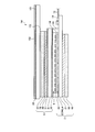
- FIG. 1 is a sectional view showing a schematic sectional structure of the display device according to the first embodiment.
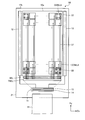
- FIG. 2 is a plan view of the first substrate of the display device according to the first embodiment.
- FIG. 3 is a circuit diagram showing a pixel array of the display device according to the first exemplary embodiment.
- FIG. 4 is a plan view of the second substrate of the display device according to the first embodiment.
- FIG. 5 is an enlarged plan view showing the region Ra shown in FIG.
- FIG. 6 is a plan view for schematically explaining the common electrode of the first embodiment.
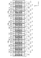
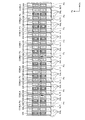
- FIG. 7A is a plan view schematically illustrating the polarities of the pixel electrode and the signal line in the first driving state in the display operation of the first embodiment.
- FIG. 7B is a plan view schematically illustrating the polarities of the pixel electrode and the signal line in the second driving state in the display operation of the first embodiment.
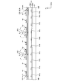
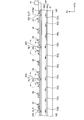
- FIG. 8A is a cross-sectional view schematically illustrating the polarities of the pixel electrode and the signal line in the first driving state in the display operation of the first embodiment.
- FIG. 8B is a cross-sectional view schematically illustrating the polarities of the pixel electrode and the signal line in the second driving state in the display operation of the first embodiment.
- FIG. 9 is a cross-sectional view schematically illustrating polarities of pixel electrodes and signal lines in a display operation in which column inversion driving is performed so that each column has a different polarity as a comparative example.
- FIG. 8A is a cross-sectional view schematically illustrating the polarities of the pixel electrode and the signal line in the first driving state in the display operation of the first embodiment.
- FIG. 8B is a cross-sectional view schematically illustrating the
- FIG. 10A is a plan view schematically illustrating the polarities of the pixel electrode and the signal line in the first driving state in the display operation of the first modification of the first embodiment.
- FIG. 10B is a plan view schematically illustrating the polarities of the pixel electrode and the signal line in the second driving state in the display operation of the first modification of the first embodiment.
- FIG. 11A is a plan view schematically illustrating the polarities of the pixel electrode and the signal line in the first driving state in the display operation of the second modification of the first embodiment.
- FIG. 11B is a plan view schematically illustrating the polarities of the pixel electrode and the signal line in the second driving state in the display operation of the second modification of the first embodiment.
- FIG. 12 is a cross-sectional view schematically illustrating the shield electrode in the third modification of the first embodiment.
- FIG. 13 is a cross-sectional view for schematically explaining the auxiliary electrode in the modified example 4 of the first embodiment.
- FIG. 14 is a plan view of the first substrate of the display device according to the second embodiment.
- FIG. 15 is a sectional view showing a schematic sectional structure of the display device according to the second embodiment.
- FIG. 16 is a plan view for schematically explaining the common electrode of the second embodiment.
- FIG. 17A is a plan view schematically illustrating the polarities of the pixel electrode and the signal line in the first driving state in the display operation of the second embodiment.
- FIG. 17B is a plan view schematically illustrating the polarities of the pixel electrode and the signal line in the second driving state in the display operation of the second embodiment.
- FIG. 18A is a cross-sectional view schematically illustrating the polarities of the pixel electrode and the signal line in the first driving state in the display operation of the second embodiment.
- FIG. 18B is a cross-sectional view schematically illustrating the polarities of the pixel electrode and the signal line in the second driving state in the display operation of the second embodiment.
- FIG. 19 is a cross-sectional view schematically illustrating the polarities of the pixel electrode and the signal line in the first driving state in the display operation of the third embodiment.
- FIG. 1 is a sectional view showing a schematic sectional structure of a display device.
- the display device 1 includes a pixel substrate 2, a counter substrate 3, and a liquid crystal layer 6 as a display function layer.
- the counter substrate 3 is arranged so as to face the surface of the pixel substrate 2 in a direction perpendicular to the surface.
- the liquid crystal layer 6 is provided between the pixel substrate 2 and the counter substrate 3.
- the display device 1 further includes a cover member 101 provided on the counter substrate 3. The cover member 101 is attached onto the polarizing plate 35 of the counter substrate 3 via the adhesive layer 102.
- the pixel substrate 2 has a first substrate 21, a pixel electrode 22, a common electrode COML, and a polarizing plate 65.
- a circuit such as a gate scanner included in the gate driver 12, a switching element Tr such as a TFT (Thin Film Transistor), various wirings such as a scanning line GCL, a signal line SGL (not shown in FIG. 1). Is shown).
- the common electrode COML is provided on the upper side of the first substrate 21.
- the pixel electrode 22 is a pixel electrode provided above the common electrode COML via the insulating layer 24.
- the pixel electrode 22 is provided in a layer different from the common electrode COML, and is arranged to overlap the common electrode COML in a plan view. Further, the pixel electrodes 22 are arranged in a matrix in a plan view.
- the polarizing plate 65 is provided below the first substrate 21 via the adhesive layer 66.
- a transparent conductive material such as ITO (Indium Tin Oxide) is used, for example.
- ITO Indium Tin Oxide
- the first substrate 21 is provided with the integrated circuit 19 and the flexible substrate 72.
- the integrated circuit 19 functions as a control unit.
- the direction from the first substrate 21 to the second substrate 31 in the direction perpendicular to the surface of the first substrate 21 is referred to as “upper side”. Further, the direction from the second substrate 31 to the first substrate 21 will be referred to as “lower side”. Further, the “plan view” refers to a case viewed from a direction perpendicular to the surface of the first substrate 21.
- the counter substrate 3 includes a second substrate 31, a color filter 32 formed on one surface of the second substrate 31, a detection electrode TDL, a protective layer 38, an adhesive layer 39, and a polarizing plate 35.
- a plurality of detection electrodes TDL are arranged on the second substrate 31.
- the detection electrode TDL is a detection electrode that detects a change in capacitance according to an object that contacts or approaches the display area.
- the flexible substrate 71 is connected to the second substrate 31.
- the detection IC 18 is mounted on the flexible substrate 71.
- the detection electrode TDL is electrically connected to the detection IC 18 via the terminal portion 36.
- the detection electrode TDL has a first thin wire 33U and a second thin wire 33V (see FIG. 4). Further, a protective layer 38 for protecting the detection electrode TDL including the first thin line 33U and the second thin line 33V is provided on the detection electrode TDL.
- a translucent resin such as an acrylic resin can be used for the protective layer 38.
- a polarizing plate 35 is provided on the protective layer 38 with an adhesive layer 39 interposed therebetween.
- the first substrate 21 and the second substrate 31 are arranged facing each other with a predetermined gap.
- the space between the first substrate 21 and the second substrate 31 is sealed by the seal portion 61.
- the liquid crystal layer 6 is provided in a space surrounded by the first substrate 21, the second substrate 31, and the seal portion 61.
- the liquid crystal layer 6 modulates the light passing therethrough according to the state of the electric field.
- a lateral electric field such as IPS (In-Plane Switching) including FFS (Fringe Field Switching). Mode liquid crystal is used.
- Alignment films are provided between the liquid crystal layer 6 and the pixel substrate 2 shown in FIG. 1, and between the liquid crystal layer 6 and the counter substrate 3, respectively.
- the liquid crystal layer 6 is driven by the horizontal electric field generated between the pixel electrode 22 and the common electrode COML.
- the illumination unit has a light source such as an LED, and emits light from the light source toward the first substrate 21.
- Light from the illumination unit passes through the pixel substrate 2, is modulated by the state of the liquid crystal at that position, and the transmission state to the display surface changes depending on the location. As a result, the image is displayed on the display surface.
- the cover member 101 is provided so as to cover the pixel substrate 2 and the counter substrate 3, and protects the pixel substrate 2 and the counter substrate 3.
- a glass substrate or a resin substrate is used as the cover member 101.
- the cover member 101 can also use a film-shaped resin material.
- the outer shape of the cover member 101 in plan view is larger than that of the first substrate 21 and the second substrate 31.
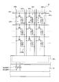
- FIG. 3 is a circuit diagram showing a pixel array of the display device according to the first exemplary embodiment.
- the switching element Tr of each sub-pixel SPix shown in FIG. 3 the signal line SGL, the scanning line GCL, and the like are formed.
- the signal line SGL is a wiring for supplying the pixel signal Vpix to each pixel electrode 22.
- the scanning line GCL is a wiring for supplying a drive signal for driving each switching element Tr.
- each sub-pixel SPix includes a switching element Tr and a liquid crystal element 6a.
- the switching element Tr is composed of a thin film transistor, and in this example, is composed of an n-channel MOS (Metal Oxide Semiconductor) type TFT.
- the insulating layer 24 is provided between the pixel electrode 22 and the common electrode COML, and these form the storage capacitor 6b shown in FIG.
- the gate driver 12 shown in FIG. 2 sequentially selects the scanning lines GCL.
- the gate driver 12 applies the scanning signal Vscan to the gate of the switching element Tr of the sub-pixel SPix via the selected scanning line GCL.
- one row (one horizontal line) of the sub-pixel SPix is sequentially selected as a display drive target.
- the source driver 13 shown in FIG. 2 supplies the pixel signal Vpix to the sub-pixels SPix forming one selected horizontal line via the signal line SGL.
- the gate driver 12 deselects the scanning line CGL
- the gate of the switching element Tr shown in FIG. 3 is turned off, and charges corresponding to the pixel signal Vpix are stored in the liquid crystal element 6a and the storage capacitor 6b.
- display is performed one horizontal line at a time according to the supplied pixel signal Vpix.
- the source driver 13 generates a switch control signal necessary for separating the pixel signal Vpix multiplexed into the image signal, and supplies it to the selector circuit SEL together with the pixel signal Vpix.
- the drive electrode driver 14 shown in FIG. 2 applies the display drive signal Vcomdc to the common electrode COML.
- the display drive signal Vcomdc is a DC voltage signal having a common potential for the plurality of sub-pixels SPix.
- each common electrode COML functions as a common electrode for the pixel electrode 22 in the display operation.
- the drive electrode driver 14 applies the display drive signal Vcomdc to all the common electrodes COML in the display area 10a.
- the display drive signal Vcomdc may be an AC signal having a predetermined cycle.
- the source driver 13 includes a positive polarity amplifier SIGAMP1 and a negative polarity amplifier SIGAMP2.
- the potential of the common electrode COML in the display operation (the potential to which the display drive signal Vcomdc is applied) is used as the reference potential.
- the positive polarity amplifier SIGAMP1 charges the signal line SGL with a drive voltage having a potential higher than the reference potential (hereinafter, referred to as positive polarity and may be represented by (+)). Circuit.
- the negative polarity amplifier SIGAMP2 charges the signal line SGL with a driving voltage of a potential lower than the reference potential (hereinafter, referred to as negative polarity and sometimes represented by ( ⁇ )). Is.
- the selector circuit SEL connects the negative polarity amplifier SIGAMP2 to the signal line SGL after a predetermined time when the positive polarity amplifier SIGAMP1 is connected to the signal line SGL based on the switch control signal from the source driver.
- the selector circuit SEL connects the positive polarity amplifier SIGAMP1 to the signal line SGL after a predetermined time.
- color regions of color filters colored in three colors of red (R), green (G), and blue (B) may be arranged periodically.
- the above-described sub-pixels SPix shown in FIG. 3 are associated with the color regions 32R, 32G, and 32B of three colors of R, G, and B as one set.
- the pixel Pix is configured with one set of sub-pixels SPix corresponding to the three color regions 32R, 32G, and 32B.
- the color filter 32 may include color regions of four or more colors.
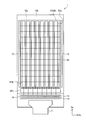
- FIG. 2 is a plan view of the first substrate of the display device according to the first embodiment.
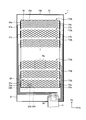
- FIG. 4 is a plan view of the second substrate of the display device according to the first embodiment.
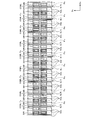
- FIG. 5 is an enlarged plan view showing the region Ra shown in FIG.
- the first substrate 21 has a region corresponding to the display region 10a and the peripheral region 10b.
- the peripheral area 10b is an area outside the display area 10a.
- the integrated circuit 19 is mounted on the peripheral region 10b of the first substrate 21.
- the integrated circuit 19 incorporates each circuit necessary for the display operation, such as a part of the functions of the drive electrode driver 14 and the source driver 13.
- the peripheral region 10b may surround the display region 10a, and in that case, the peripheral region 10b can be said to be a frame region.
- the remaining parts of the gate driver 12 and the source driver 13 such as a multiplexer are formed on the first substrate 21 which is a glass substrate.
- the integrated circuit 19 may be arranged on the first substrate 21 substrate without incorporating the drive electrode driver 14.
- the peripheral region 10b can be narrowed.
- the flexible substrate 72 is connected to the integrated circuit 19, and a video signal and a power supply voltage are externally supplied to the integrated circuit 19 via the flexible substrate 72.
- a plurality of common electrodes COML are provided in a region overlapping the display region 10a of the first substrate 21.
- Each of the plurality of common electrodes COML extends in the direction along the long side of the display region 10a (second direction Dy), and is spaced in the direction along the short side of the display region 10a (first direction Dx).
- the plurality of common electrodes COML are connected to the drive electrode driver 14, respectively.
- the third direction Dz is a thickness direction perpendicular to the plane of the first direction Dx and the second direction Dy.
- the common electrode COML extends in the direction intersecting the scanning line GCL.
- the common electrode COML extends in the direction parallel to the signal line SGL.
- the wiring connected to the common electrode COML and the drive electrode driver 14 can be formed in the integrated circuit.
- the gate driver 12 is provided on the long side of the peripheral region 10b, and the drive electrode driver 14 and the source driver 13 are on the flexible substrate 72 of the short side of the peripheral region 10b. Is provided on the connected side. Therefore, the display device 1 of the present embodiment is advantageous in narrowing the frame of the peripheral region 10b in the portion along the common electrode COML.
- a plurality of detection electrodes TDL are provided in a region overlapping the display region 10a of the second substrate 31.
- Each of the plurality of detection electrodes TDL extends in a direction (first direction Dx) intersecting the extension direction of the common electrode COML shown in FIG.
- the plurality of detection electrodes TDL are arranged at intervals SP in the extending direction (second direction Dy) of the common electrode COML. That is, the plurality of common electrodes COML and the plurality of detection electrodes TDL are arranged so as to intersect with each other in a plan view, and a capacitance is formed in a portion where they overlap each other.
- the display device 1 sequentially applies the drive signal Vdet from the drive electrode driver 14 to the common electrode COML to sequentially scan one detection line at a time. That is, the display unit 10 performs sensing scanning in parallel with the first direction Dx along one side of the display unit 10.
- the detection electrode TDL outputs a detection signal to the detection unit 40.
- capacitance detection of one detection block is performed. That is, the common electrode COML corresponds to the drive electrode E1 and the detection electrode TDL corresponds to the detection electrode E2 in the detection of the mutual capacitance described in Patent Document 2 described above (FIG. 4 of Patent Document 2).
- the detection electrodes TDL and the common electrodes COML intersecting with each other form a capacitive touch sensor in a matrix. Therefore, by scanning over the entire detection surface, it is possible to detect the position where the conductor comes into contact or approaches from the outside.
- the contents of Japanese Patent Laid-Open No. 2014-132446 are incorporated herein as a part of the present disclosure.
- the display device 1 performs the detection operation (detection period) and the display operation (display operation period) in a time-sharing manner.
- the detecting operation and the displaying operation may be performed separately.
- the common electrode COML also functions as a common electrode with respect to the pixel electrode 22. Therefore, during the display operation period, all the common electrodes COML have the display drive voltage that is the common electrode potential for display.
- the signal Vcomdc is supplied via the drive electrode driver 14.
- the drive electrode driver 14 uses the detection electrode
- the drive signal Vdet for detection may be supplied to TDL.
- the detection electrode TDL of this embodiment has a plurality of first thin wires 33U and a plurality of second thin wires 33V.
- the first thin line 33U and the second thin line 33V are inclined in directions opposite to each other with respect to the direction parallel to one side of the display area 10a.
- the first thin line 33U forms a first angle with the first direction Dx
- the second thin line 33V forms a second angle with the first direction Dx.
- the plurality of first thin wires 33U and the second thin wires 33V are thin metal wires having conductivity.
- the plurality of first thin lines 33U are arranged at intervals in the second direction Dy.
- the plurality of second thin wires 33V are arranged at intervals in the second direction Dy.
- the detection electrode TDL includes at least one first thin wire 33U and at least one second thin wire 33V intersecting with the first thin wire 33U.
- the first thin wire 33U and the second thin wire 33V are electrically connected by the connecting portion 33X.
- the shape of one mesh of the detection electrodes TDL becomes a parallelogram.
- Both ends of the plurality of first thin wires 33U and second thin wires 33V in the extending direction are connected to the connection wirings 34a and 34b arranged in the peripheral region 10b.
- the first thin wire 33U and the second thin wire 33V which are the main detection portions of the detection electrode TDL, are connected to the connection wirings 34a and 34b via the thin wire 33a. Accordingly, the plurality of first thin wires 33U and the second thin wires 33V are electrically connected to each other and function as one detection electrode TDL.
- the first thin wire 33U and the second thin wire 33V are selected from aluminum (Al), copper (Cu), silver (Ag), molybdenum (Mo), chromium (Cr), titanium (Ti) and tungsten (W). It is formed of one or more metal layers. Alternatively, the first thin wire 33U and the second thin wire 33V are formed of an alloy containing at least one selected from these metal materials.
- the detection electrode TDL includes a sensor part TDLs and a dummy part TDLd.
- the sensor portion TDLs and the dummy portion TDLd extend in the first direction Dx and are arranged alternately in the second direction Dy.
- the sensor unit TDLs is connected to the connection wirings 34a and 34b shown in FIG. 4 and mainly functions as a detection electrode.
- the dummy part TDLd is provided so as to be electrically separated from the sensor part TDLs and the connection wirings 34a and 34b.
- the dummy part TDLd is a dummy electrode that does not function as a detection electrode.
- the sensor unit TDLs and the dummy unit TDLd each include the above-described first thin wire 33U and second thin wire 33V, and have a mesh-like configuration similar to each other. As a result, it is possible to suppress variations in light transmittance in the display area 10a and obtain good visibility.
- the sensor part TDLs and the dummy part TDLd are electrically separated by the slit SLM provided in the first thin wire 33U and the second thin wire 33V.
- the slits SLM are provided in the first thin lines 33U and the second thin lines 33V that form one mesh of the dummy portion TDLd.
- the first wiring 37a is connected to each of the plurality of connection wirings 34a.
- the second wiring 37b is connected to each of the plurality of connection wirings 34b. That is, in the present embodiment, the first wiring 37a is connected to one end side of the detection electrode TDL, and the second wiring 37b is connected to the other end side.
- the first wiring 37a is provided along one of the long sides of the peripheral region 10b.
- the second wiring 37b is provided along the other long side of the peripheral region 10b.
- the first wiring 37a and the second wiring 37b connected to one detection electrode TDL are connected to one terminal portion 36. That is, the detection electrode TDL, the first wiring 37a, the second wiring 37b, and the terminal portion 36 are connected in a loop.
- the detection electrode TDL is connected to the flexible substrate 71 via the first wiring 37a, the second wiring 37b, and the terminal portion 36.
- one of the first wiring 37a and the second wiring 37b may be connected to one detection electrode TDL.
- the detection electrode TDL is not limited to the mesh-shaped thin metal wire, and may be configured to include a plurality of zigzag-shaped metal wires or wavy-shaped metal thin wires, for example.
- the sensor part TDLs and the dummy part TDLd included in one detection electrode TDL are shown in FIG. 5, the dummy electrode may be arranged in the interval SP between the detection electrodes TDL.
- FIG. 6 is a plan view for schematically explaining the common electrode of the first embodiment. Note that FIG. 6 shows the three common electrodes COML in an enlarged manner.
- a slit SLT (inter-electrode slit) extending in the second direction Dy is provided between the adjacent common electrodes COML.
- a slit SLTI (in-electrode slit) extending in the second direction Dy is provided inside each common electrode COML.
- the slit SLTI is called a dummy slit for making the slit SLT invisible. Therefore, the ends of the slit SLTI in the second direction Dy are connected by a conductive material. If the distance between the two slits SLTI and the distance between the slits SLTI and the slits SLT are the same, the slits SLT are less noticeable.
- the width of the slit SLT in the first direction Dx is about 1 ⁇ m or more and 5 ⁇ m or less.
- the width of the slit SLTI in the first direction Dx is about 1 ⁇ m or more and 5 ⁇ m or less.
- FIG. 7A is a plan view schematically illustrating the polarities of the pixel electrode and the signal line in the first driving state in the display operation of the first embodiment.
- FIG. 7B is a plan view schematically illustrating the polarities of the pixel electrode and the signal line in the second driving state in the display operation of the first embodiment.
- FIG. 8A is a cross-sectional view schematically illustrating the polarities of the pixel electrode and the signal line in the first driving state in the display operation of the first embodiment.
- FIG. 8A is a schematic view of a VIII-VIII′ cross section of FIG. 7A.
- FIG. 8B is a cross-sectional view schematically illustrating the polarities of the pixel electrode and the signal line in the second driving state in the display operation of the first embodiment.
- the signal line SGL supplies the pixel signal Vpix to the pixel electrode 22 (see FIGS. 8A and 8B) on the right side in the first direction Dx shown in FIGS. 7A and 7B.
- the pixel signal Vpix is supplied from the signal line SGL to the pixel electrode 22 on the right side in the first direction Dx shown in FIGS. 7A and 7B via the switching element Tr.
- FIGS. 7A and 7B illustration of the switching element Tr is omitted. Then, during the display operation, the first drive state shown in FIG. 7A and the second drive state shown in FIG. 7B are alternately generated in a predetermined cycle.
- FIG. 9 is a cross-sectional view schematically illustrating the polarities of pixel electrodes and signal lines in a display operation in which column inversion driving is performed so that the polarities are different for each column as a comparative example.
- the first insulating layer 24a and the second insulating layer 24b are laminated to form the insulating layer 24.
- the signal line SGL is alternately driven in the positive direction and in the negative direction in the first direction Dx.
- the third direction Dz is a direction perpendicular to the plane of the first direction Dx and the second direction Dy.
- One of the pixel electrodes 22 adjacent to the slit SLT of the comparative example is driven with a positive polarity and the other is driven with a negative polarity.
- the electric field of the signal line SGL leaks to the pixel electrode side through the slit SLT.
- a difference occurs in the electric field distribution between the electrode 22 and the signal line SGL.
- one of the pixel electrodes 22 adjacent to the slit SLTI of the comparative example is driven with a positive polarity and the other is driven with a negative polarity.
- the electric field of the signal line SGL leaks through the slit SLTI.
- the difference in electric field distribution generated in the comparative example forms electric convection in the liquid crystal layer, and as a result, ions existing in the liquid crystal layer 6 (see FIG. 1) may be partially accumulated. Then, the difference between the portion where the ions are accumulated and the portion where the ions are not accumulated may be visually recognized as a reduction in display quality.
- the signal line SGL overlapping the slit SLT in the third direction Dz is driven by the negative drive voltage. ..
- the pixel electrodes 22 adjacent to the slit SLT are both driven with a negative polarity.
- the pixel electrode 22 adjacent to the slit SLT is driven with the same polarity as the signal line SGL overlapping the slit SLT.
- the display device 1 drives the signal line SGL overlapping the slit SLT in the third direction Dz with a positive drive voltage. ..
- the pixel electrodes 22 adjacent to the slit SLT are both driven with a positive polarity.
- the display device 1 of the first embodiment includes the first substrate 21, the plurality of scanning lines GCL, the plurality of signal lines SGL, the common electrode COML, and the pixel electrode 22.
- the scanning line GCL extends in the first direction Dx of the first substrate 21.
- the signal line SGL extends in the second direction Dy intersecting the first direction Dx of the first substrate 21.
- the common electrode COML is provided on the first substrate 21, and the pixel electrode 22 overlaps the common electrode COML in plan view.
- the slit SLT first slit
- the polarity of the drive voltage of the signal line SGL overlapping the slit SLT is the same as the polarity of the drive voltage of the two pixel electrodes 22 adjacent to each other in the first direction Dx of the slit SLT.
- the pixel electrodes 22 adjacent to each other with the slit SLT in between produce the same electric field distribution with respect to the signal line SGL overlapping the slit SLT.
- the accumulation of ions is less likely to occur around the slit SLT.
- the display device 1 according to the first embodiment can suppress deterioration of display quality.
- a slit SLTI (second slit) extending in the second direction Dy.
- the slit SLTI overlaps with one of the signal lines SGL in plan view. Then, in the display operation, the polarity of the drive voltage of the signal line SGL overlapping the slit SLTI is the same as the polarity of the drive voltage of the two pixel electrodes 22 adjacent to the slit SLTI.
- the pixel electrodes 22 adjacent to each other with the slit SLTI in between produce the same electric field distribution with respect to the signal line SGL overlapping the slit SLTI.
- the accumulation of ions is less likely to occur around the slit SLTI.
- the display device 1 according to the first embodiment can suppress deterioration of display quality.
- the polarity of the drive voltage of the signal line SGL overlapping the slit SLT and the polarities of the two pixel electrodes 22 adjacent to the slit SLT are inverted at a predetermined cycle. Further, the polarity of the drive voltage of the signal line SGL overlapping the slit SLTI and the polarities of the two pixel electrodes 22 adjacent to the slit SLTI are inverted at a predetermined cycle. As a result, it is possible to suppress a display defect called so-called burn-in of the liquid crystal layer 6.
- the drive voltage of two adjacent signal lines SGL has a positive polarity and the drive voltage of two adjacent signal lines SGL. Has a negative polarity. As a result, the charge and discharge due to the inversion of the polarity is small, and the display device 1 has low power consumption.
- two signal lines SGL overlap with the common electrode COML in plan view. Further, in plan view, the two signal lines SGL overlapping the common electrode COML are adjacent to each other in the first direction Dx.
- the signal line SGL between the slit SLT and the slit SLTI overlaps the common electrode COML in plan view.
- the electric field from the signal line SGL covered with the common electrode COML hardly reaches the pixel electrode 22. Therefore, even if the polarity of the drive voltage of the signal line SGL covered with the common electrode COML and the polarity of the drive voltage of the pixel electrode 22 adjacent to the signal line SGL are different, the deterioration of the display quality is suppressed.
- the common electrode COML extends in the second direction Dy.
- the display device 1 includes a plurality of detection electrodes TDL, and the plurality of detection electrodes TDL face the plurality of common electrodes COML in the third direction Dz direction (thickness direction) and extend in the first direction Dx. Capacitively coupled to the plurality of common electrodes COML. Accordingly, the display device 1 can detect an object that is in contact with or close to the display area.
- FIG. 10A is a plan view schematically illustrating the polarities of the pixel electrode and the signal line in the first driving state in the display operation of the first modification of the first embodiment.
- FIG. 10B is a plan view schematically illustrating the polarities of the pixel electrode and the signal line in the second driving state in the display operation of the first modification of the first embodiment.
- illustration of the switching element Tr is omitted.
- the same components as those described in each of the above-described embodiments are denoted by the same reference numerals, and duplicate description will be omitted.
- the first drive state shown in FIG. 10A and the second drive state shown in FIG. 10B alternate with each other in a predetermined cycle.
- two signal lines SGL overlap with the common electrode COML in a plan view.
- the signal line SGL between the slit SLT and the slit SGLI overlaps the common electrode COML in plan view.
- the two signal lines SGL overlapping the common electrode COML are adjacent to the signal line SGL overlapping the slit SLT or the slit SGLI in plan view.
- the electric field from the signal line SGL covered with the common electrode COML hardly reaches the pixel electrode 22.
- the display device 1 of the first embodiment is driven in reverse, and as illustrated in FIG. 10A, the signal line SGL overlapping the slit SLT in the third direction Dz is driven by a positive drive voltage.
- the pixel electrodes 22 adjacent to the slit SLT are both driven with a positive polarity. For this reason, the pixel electrodes 22 adjacent to each other with the slit SLT in between generate the same electric field distribution with respect to the signal line SGL overlapping the slit SLT. Thereby, even if the polarity of the drive voltage is reversed, the accumulation of ions is less likely to occur around the slit SLT.
- the display device 1 is driven in reverse, and as illustrated in FIG. 10B, the signal line SGL overlapping the slit SLT in the third direction Dz is driven with a negative drive voltage.
- the pixel electrodes 22 adjacent to the slit SLT are both driven with a negative polarity. For this reason, the pixel electrodes 22 adjacent to each other with the slit SLT in between produce the same electric field distribution with respect to the signal line SGL overlapping the slit SLT. Thereby, even if the polarity of the drive voltage is reversed, the accumulation of ions is less likely to occur around the slit SLT.
- FIG. 11A is a plan view schematically illustrating the polarities of the pixel electrode and the signal line in the first driving state in the display operation of the second modification of the first embodiment.
- FIG. 11B is a plan view schematically illustrating the polarities of the pixel electrode and the signal line in the second driving state in the display operation of the second modification of the first embodiment.
- the illustration of the switching element Tr is omitted.
- the same components as those described in each of the above-described embodiments are denoted by the same reference numerals, and duplicate description will be omitted.
- the first drive state shown in FIG. 11A and the second drive state shown in FIG. 11B alternate with each other in a predetermined cycle.
- the slit SLTI is not provided.
- the display device 1 of the first embodiment is driven in reverse, and as illustrated in FIG. 11A, the signal line SGL overlapping the slit SLT in the third direction Dz is driven with a negative drive voltage.
- the pixel electrodes 22 adjacent to the slit SLT are both driven with a negative polarity. For this reason, the pixel electrodes 22 adjacent to each other with the slit SLT in between produce the same electric field distribution with respect to the signal line SGL overlapping the slit SLT. Thereby, even if the polarity of the drive voltage is reversed, the accumulation of ions is less likely to occur around the slit SLT.
- the display device 1 of the first embodiment is driven in reverse, and as illustrated in FIG. 11B, the signal line SGL overlapping the slit SLT in the third direction Dz is driven with a positive drive voltage.
- the pixel electrodes 22 adjacent to the slit SLT are both driven with a positive polarity. For this reason, the pixel electrodes 22 adjacent to each other with the slit SLT in between produce the same electric field distribution with respect to the signal line SGL overlapping the slit SLT. Thereby, even if the polarity of the drive voltage is reversed, the accumulation of ions is less likely to occur around the slit SLT.
- FIG. 12 is a cross-sectional view schematically illustrating the shield electrode in the third modification of the first embodiment.
- the same components as those described in each of the above-described embodiments are denoted by the same reference numerals, and duplicate description will be omitted.
- the shield electrode 22S overlaps the slit SLT when viewed in the third direction Dz.
- the shield electrode 22S extends in the direction along the slit SLT or the slit SLTI when seen in a plan view.
- the shield electrode 22S is located between the pixel electrodes 22 adjacent to each other in the first direction Dx, and is formed in the same layer as the pixel electrode 22.
- a transparent conductive material such as ITO is used.
- the same voltage as that of the common electrode COML, for example, is applied to the shield electrode 22S during the display operation. Thereby, the shield electrode 22S suppresses the electric field of the signal line SGL from leaking through the slit SLT or the slit SLTI.
- FIG. 13 is a cross-sectional view for schematically explaining the auxiliary electrode in the modified example 4 of the first embodiment.
- the same components as those described in each of the above-described embodiments are denoted by the same reference numerals, and duplicate description will be omitted.
- the auxiliary electrode ML overlaps a part of the slit SLT or the slit SLTI when viewed in the third direction Dz.
- the auxiliary electrode ML is formed on the common electrode COML and is electrically connected to the common electrode COML.
- the auxiliary electrode ML is one or more metal layers selected from aluminum (Al), copper (Cu), silver (Ag), molybdenum (Mo), chromium (Cr), titanium (Ti) and tungsten (W). It is formed.
- the same voltage as that of the common electrode COML is applied to the auxiliary electrode ML during the display operation.
- the auxiliary electrode ML has a smaller sheet resistance value per unit area than the common electrode COML.
- the voltages of the plurality of common electrodes COML are likely to be constant. Further, the time constant of the drive signal can be reduced in the electrostatic capacitance detection operation. Then, a high frequency can be used as the frequency of the drive signal for driving the common electrode COML. As a result, in the display device 1, the accuracy of detecting the capacitance is improved.
- FIG. 14 is a plan view of the first substrate of the display device according to the second embodiment.
- FIG. 15 is a sectional view showing a schematic sectional structure of the display device according to the second embodiment.
- FIG. 16 is a plan view for schematically explaining the common electrode of the second embodiment.
- FIG. 17A is a plan view schematically illustrating the polarities of the pixel electrode and the signal line in the first driving state in the display operation of the second embodiment.
- FIG. 17B is a plan view schematically illustrating the polarities of the pixel electrode and the signal line in the second driving state in the display operation of the second embodiment.
- FIG. 18A is a cross-sectional view schematically illustrating the polarities of the pixel electrode and the signal line in the first driving state in the display operation of the second embodiment.
- FIG. 18B is a cross-sectional view schematically illustrating the polarities of the pixel electrode and the signal line in the second driving state in the display operation of the second embodiment.
- the illustration of the switching element Tr is omitted.
- the same components as those described in each of the above-described embodiments are denoted by the same reference numerals, and duplicate description will be omitted.
- a plurality of common electrodes COMLA are arranged in a matrix in the display area 10 a of the first substrate 21.
- the common electrodes COMLA are arranged in the first direction Dx and are arranged in the second direction Dy.
- a plurality of pixel electrodes 22 are arranged so as to overlap with one common electrode COMLA. Note that, although FIG. 14 illustrates some of the common electrodes COMLA and the pixel electrodes 22, the common electrodes COMLA and the pixel electrodes 22 are arranged in a matrix in the entire area of the display area 10a.
- the common electrode COMLA is connected to the drive electrode driver 14 via the wiring 37, respectively.
- the drive electrode driver 14 supplies the display drive signal Vcomdc to all the common electrodes COMLA via the selector circuit TSEL.
- the drive electrode driver 14 supplies the drive signal Vdet to the common electrode COMLA via the selector circuit TSEL simultaneously or sequentially.
- the common electrode COMLA outputs to the integrated circuit 19 a detection signal corresponding to a change in the capacitance of the common electrode COMLA.
- the capacitance of the detection surface is detected based on the detection signal from each common electrode COMLA. That is, the common electrode COMLA functions as a common electrode during the display operation and also as a detection electrode during the detection of the self-capacitance.
- the wiring 37 is provided in a different layer from the common electrode COMLA via the insulating layer 24b, and is provided so as to overlap the common electrode COMLA and the slit SLTY in a plan view.
- a slit SLTX extending in the first direction Dx is provided between the adjacent common electrodes COMLA.
- a slit SLTY extending in the second direction Dy is provided between the adjacent common electrodes COMLA.
- a slit SLTI extending in the second direction Dy is provided inside each common electrode COMLA.
- the slit SLTI is called a dummy slit for making the slit SLTY invisible. Therefore, the ends of the slit SLTI in the second direction Dy are connected by a conductive material. If the distance between the two slits SLTI and the distance between the slit SLTI and the slit SLTY are the same, the slit SLTY becomes inconspicuous.
- the width of the slit SLTY in the first direction Dx is about 1 ⁇ m or more and 5 ⁇ m or less.
- the width of the slit SLTI in the first direction Dx is about 1 ⁇ m or more and 5 ⁇ m or less.
- the signal line SGL overlapping the slit SLTY in the third direction Dz is driven with a negative drive voltage.
- the pixel electrodes 22 adjacent to the slit SLTY are both driven with a negative polarity.
- the pixel electrode 22 adjacent to the slit SLTY is driven with the same polarity as the signal line SGL overlapping the slit SLTY.
- the pixel electrodes 22 adjacent to each other with the slit SLTY in between generate the same electric field distribution with respect to the signal line SGL overlapping the slit SLTY.
- the accumulation of ions is less likely to occur around the slit SLTY.
- the display device 1 according to the second embodiment is driven by the positive drive voltage of the signal line SGL overlapping the slit SLTY in the third direction Dz. .
- the pixel electrodes 22 adjacent to the slit SLTY are both driven with a positive polarity. Therefore, the pixel electrodes 22 that are adjacent to each other with the slit SLTY in between generate the same electric field distribution with respect to the signal line SGL that overlaps with the slit SLTY. Thereby, even if the polarity of the drive voltage is reversed, the accumulation of ions is less likely to occur around the slit SLT.
- the display device 1 of the second embodiment includes the first substrate 21, the plurality of scanning lines GCL, the plurality of signal lines SGL, the common electrode COMLA, and the pixel electrode 22.
- the scanning line GCL extends in the first direction Dx of the first substrate 21.
- the signal line SGL extends in the second direction Dy intersecting the first direction Dx of the first substrate 21.
- the common electrode COMLA is provided on the first substrate 21, and the pixel electrode 22 overlaps the common electrode COMLA in plan view.
- the slit SLTY first slit
- the polarity of the drive voltage of the signal line SGL overlapping the slit SLTY is the same as the polarity of the drive voltage of the two pixel electrodes 22 adjacent to each other in the first direction Dx of the slit SLTY.
- the pixel electrodes 22 adjacent to each other with the slit SLTY in between produce the same electric field distribution with respect to the signal line SGL overlapping the slit SLTY.
- the accumulation of ions is less likely to occur around the slit SLTY.
- the display device 1 according to the second embodiment can suppress deterioration of display quality.
- a slit SLTI (second slit) extending in the second direction Dy.
- the slit SLTI overlaps with one of the signal lines SGL in plan view. Then, in the display operation, the polarity of the drive voltage of the signal line SGL overlapping the slit SLTI is the same as the polarity of the drive voltage of the two pixel electrodes 22 adjacent to the slit SLTI.
- the pixel electrodes 22 adjacent to each other with the slit SLTI in between generate the same electric field distribution with respect to the signal line SGL overlapping the slit SLTI.
- the accumulation of ions is less likely to occur around the slit SLTI.
- the display device 1 according to the second embodiment can suppress deterioration of display quality.
- FIG. 19 is a cross-sectional view schematically illustrating the polarities of the pixel electrode and the signal line in the first driving state in the display operation of the third embodiment.
- the same components as those described in each of the above-described embodiments are denoted by the same reference numerals, and duplicate description will be omitted.
- the gate driver 12, the source driver 13, or the drive electrode driver 14 is not formed on the first substrate 21 which is a glass substrate as in the first embodiment, but via the flexible substrate 72 described above. Thus, it may be arranged at a place different from the first substrate 21.
- the drive electrode driver 14 arranged at a place different from the first substrate 21 applies the same voltage as the common electrode COML to the shield electrode 22S during the display operation. Thereby, the shield electrode 22S suppresses the electric field of the signal line SGL from leaking through the slit SLT or the slit SLTI.
- the aspects of the modified examples 1 to 4 of the first embodiment may be applied to the aspect of the display device 1 of the second or third embodiment.
- the plane defined by the first direction Dx and the second direction Dy is parallel to the surface of the first substrate 21, but the surface of the first substrate 21 may be curved.
- the predetermined direction is the first direction
- the direction intersecting the first direction is the second direction.
- the direction viewed by the display device 1 in the maximum area may be defined as the third direction orthogonal to the first direction and the second direction.
- Display Device 2 Pixel Substrate 3 Counter Substrate 6 Liquid Crystal Layer 10
- Display Unit 14 Drive Electrode Driver 18 Detection IC 19 integrated circuit 21 first substrate 22 pixel electrode 22S shield electrode 31 second substrate COML, COMLA common electrode ML auxiliary electrode SEL selector circuit SGL signal line SLT, SLTI, SLTX, SLTY slit TDL detection electrode
Landscapes
- Physics & Mathematics (AREA)
- Nonlinear Science (AREA)
- Engineering & Computer Science (AREA)
- General Physics & Mathematics (AREA)
- Crystallography & Structural Chemistry (AREA)
- Chemical & Material Sciences (AREA)
- Optics & Photonics (AREA)
- Mathematical Physics (AREA)
- Theoretical Computer Science (AREA)
- Computer Hardware Design (AREA)
- Liquid Crystal (AREA)
- Microelectronics & Electronic Packaging (AREA)
- Liquid Crystal Display Device Control (AREA)
- Control Of Indicators Other Than Cathode Ray Tubes (AREA)
Abstract
表示品位の劣化を抑制した表示装置を提供する。表示装置において、共通電極は、第1方向に隣り合う第1共通電極と第2共通電極とを備え、第1共通電極と第2共通電極との間には第2方向に延びる電極間スリットが設けられている。画素電極は、第1共通電極に重畳する第1画素電極と、第2共通電極に重畳する第2画素電極とを備え、第1画素電極は第1信号線から画素信号が供給され、第2画素電極は第2信号線から画素信号が供給される。これら一対の第1画素電極と第2画素電極とは平面視で電極間スリットを介して隣り合って設けられており、電極間スリットは、平面視で、第2信号線と重畳しており、表示動作において、第2信号線の極性は、第1画素電極の極性及び第2画素電極の極性と同じである。
Description
本発明は、表示装置に関する。
特許文献1及び特許文献2には、表示領域に接触又は近接する物体を検出する機能を備えた表示装置が記載されている。
また、画像表示パネルの駆動方式として、カラム反転、ライン反転、ドット反転及びフレーム反転などの駆動方式が知られている。カラム反転は、副画素又は副画素が組み合わされた画素の隣り合う1ライン(列)が互いに基準の電位に対して電位が異なるように、電圧を印加し、印加する当該電圧の極性を所定の周期で反転する駆動方式である。これにより、ドット反転の駆動方式に比較して、カラム反転の駆動方式は信号線における充放電が少なく低消費電力になることが知られている(例えば、特許文献2参照)。
特許文献1及び特許文献2において、電極の間に、走査信号線の延在方向に延びるスリットがある。カラム反転の駆動により、正極性又は負極性に印加された走査線の電界がスリットを介して漏れると、表示品位が低下する可能性がある。
本発明は、表示品位の劣化を抑制した表示装置を提供することを目的とする。
本発明の一態様の表示装置は、基板と、前記基板の第1方向に延在する複数の走査線と、前記基板の前記第1方向とは交差する第2方向に延在する複数の信号線と、前記基板に設けられた複数の共通電極と、前記共通電極と、平面視で重畳する複数の画素電極と、を備え、前記共通電極は、前記第1方向に隣り合う第1共通電極と第2共通電極とを備え、前記第1共通電極と前記第2共通電極との間には第2方向に延びる電極間スリットが設けられており、前記画素電極は、前記第1共通電極に重畳する第1画素電極と、前記第2共通電極に重畳する第2画素電極とを備え、前記第1画素電極は第1信号線から画素信号が供給され、前記第2画素電極は第2信号線から画素信号が供給され、これら一対の前記第1画素電極と前記第2画素電極とは平面視で前記電極間スリットを介して隣り合って設けられており、前記電極間スリットは、平面視で、前記第2信号線と重畳しており、表示動作において、前記第2信号線の極性は、前記第1画素電極の極性及び前記第2画素電極の極性と同じである。
本開示を実施するための形態(実施形態)につき、図面を参照しつつ詳細に説明する。以下の実施形態に記載した内容により本開示が限定されるものではない。また、以下に記載した構成要素には、当業者が容易に想定できるもの、実質的に同一のものが含まれる。さらに、以下に記載した構成要素は適宜組み合わせることが可能である。なお、開示はあくまで一例にすぎず、当業者において、発明の主旨を保っての適宜変更について容易に想到し得るものについては、当然に本開示の範囲に含有されるものである。また、図面は説明をより明確にするため、実際の態様に比べ、各部の幅、厚さ、形状等について模式的に表される場合があるが、あくまで一例であって、本開示の解釈を限定するものではない。また、本明細書と各図において、既出の図に関して前述したものと同様の要素には、同一の符号を付して、詳細な説明を適宜省略することがある。
(実施形態1)
図1は、表示装置の概略断面構造を表す断面図である。図1に示すように、表示装置1は、画素基板2と、対向基板3と、表示機能層としての液晶層6とを備える。対向基板3は、画素基板2の表面に垂直な方向に対向して配置される。液晶層6は画素基板2と対向基板3との間に設けられる。表示装置1は、さらに、対向基板3に設けられたカバー部材101を備える。カバー部材101は、対向基板3の偏光板35の上に接着層102を介して貼り合わされる。
図1は、表示装置の概略断面構造を表す断面図である。図1に示すように、表示装置1は、画素基板2と、対向基板3と、表示機能層としての液晶層6とを備える。対向基板3は、画素基板2の表面に垂直な方向に対向して配置される。液晶層6は画素基板2と対向基板3との間に設けられる。表示装置1は、さらに、対向基板3に設けられたカバー部材101を備える。カバー部材101は、対向基板3の偏光板35の上に接着層102を介して貼り合わされる。
画素基板2は、第1基板21と、画素電極22と、共通電極COMLと、偏光板65とを有する。第1基板21には、ゲートドライバ12に含まれるゲートスキャナ等の回路や、TFT(Thin Film Transistor)等のスイッチング素子Trや、走査線GCL、信号線SGL等の各種配線(図1では省略して示す)が設けられる。
共通電極COMLは、第1基板21の上側に設けられる。画素電極22は、絶縁層24を介して共通電極COMLの上側に設けられる画素電極である。画素電極22は、共通電極COMLとは異なる層に設けられ、平面視で、共通電極COMLと重畳して配置される。また、画素電極22は、平面視でマトリクス状に複数配置される。偏光板65は、接着層66を介して第1基板21の下側に設けられる。画素電極22及び共通電極COMLには、例えば、ITO(Indium Tin Oxide)等の透光性を有する導電性材料が用いられる。なお、本実施形態では、画素電極22が共通電極COMLの上側に設けられる例について説明したが、共通電極COMLが画素電極22の上側に設けられていてもよい。
また、第1基板21には、集積回路19と、フレキシブル基板72が設けられる。集積回路19は、制御部として機能する。
なお、本開示において、第1基板21の表面に垂直な方向において、第1基板21から第2基板31に向かう方向を「上側」とする。また、第2基板31から第1基板21に向かう方向を「下側」とする。また、「平面視」とは、第1基板21の表面に垂直な方向からみた場合を示す。
対向基板3は、第2基板31と、第2基板31の一方の面に形成されたカラーフィルタ32と、検出電極TDLと、保護層38と、接着層39と、偏光板35とを有する。検出電極TDLは、第2基板31の上に複数配列されている。検出電極TDLは、表示領域に接触又は近接する物体に応じた静電容量の変化を検出する検出電極である。第2基板31にはフレキシブル基板71が接続されている。フレキシブル基板71には、検出用IC18が搭載されている。検出電極TDLは、端子部36を介して、検出用IC18に電気的に接続される。
検出電極TDLは、第1細線33U及び第2細線33Vを有している(図4参照)。さらに、検出電極TDLの上には、第1細線33U及び第2細線33Vを含む検出電極TDLを保護するための保護層38が設けられている。保護層38は、アクリル系樹脂等の透光性樹脂を用いることができる。保護層38の上に、接着層39を介して偏光板35が設けられている。
図1に示すように、第1基板21と第2基板31とは所定の間隔を設けて対向して配置される。第1基板21と第2基板31との間の空間は、シール部61により封止される。第1基板21、第2基板31、及びシール部61によって囲まれた空間に液晶層6が設けられる。液晶層6は、通過する光を電界の状態に応じて変調するものであり、例えば、FFS(Fringe Field Switching:フリンジフィールドスイッチング)を含むIPS(In-Plane Switching:インプレーンスイッチング)等の横電界モードの液晶が用いられる。なお、図1に示す液晶層6と画素基板2との間、及び液晶層6と対向基板3との間には、それぞれ配向膜が配設される。本実施形態では、画素電極22と共通電極COMLとの間に発生する横電界により、液晶層6が駆動される。
第1基板21の下側には、図示しない照明部(バックライト)が設けられる。照明部は、例えばLED等の光源を有しており、光源からの光を第1基板21に向けて射出する。照明部からの光は、画素基板2を通過して、その位置の液晶の状態により変調され、表示面への透過状態が場所によって変化する。これにより、表示面に画像が表示される。
カバー部材101は、画素基板2及び対向基板3を覆って設けられ、画素基板2及び対向基板3を保護する。カバー部材101は、例えば、ガラス基板や樹脂基板が用いられる。また、カバー部材101は、フィルム状の樹脂材料を用いることもできる。カバー部材101の平面視での外形形状は、第1基板21及び第2基板31よりも大きい。
次に表示装置1の表示動作について説明する。図3は、実施形態1に係る表示装置の画素配列を表す回路図である。第1基板21(図1参照)には、図3に示す各副画素SPixのスイッチング素子Tr、信号線SGL、走査線GCL等が形成されている。信号線SGLは、各画素電極22に画素信号Vpixを供給するための配線である。走査線GCLは、各スイッチング素子Trを駆動する駆動信号を供給するための配線である。
図3に示すように、複数の副画素SPixは、マトリクス状に配列されている。副画素SPixは、それぞれスイッチング素子Tr及び液晶素子6aを備えている。スイッチング素子Trは、薄膜トランジスタにより構成されるものであり、この例では、nチャネルのMOS(Metal Oxide Semiconductor)型のTFTで構成されている。画素電極22と共通電極COMLとの間に絶縁層24が設けられ、これらによって図3に示す保持容量6bが形成される。
図2に示すゲートドライバ12は、走査線GCLを順次選択する。ゲートドライバ12は、選択された走査線GCLを介して、走査信号Vscanを副画素SPixのスイッチング素子Trのゲートに印加する。これにより、副画素SPixのうちの1行(1水平ライン)が表示駆動の対象として順次選択される。また、図2に示すソースドライバ13は、選択された1水平ラインを構成する副画素SPixに、信号線SGLを介して画素信号Vpixを供給する。ゲートドライバ12が走査線CGLを非選択とすると、図3に示すスイッチング素子Trのゲートがオフ状態となり、液晶素子6a及び保持容量6bに、画素信号Vpixに応じた電荷が蓄えられる。そして、これらの副画素SPixでは、供給される画素信号Vpixに応じて1水平ラインずつ表示が行われるようになっている。
ソースドライバ13は、画像信号に多重化された画素信号Vpixを分離するために必要なスイッチ制御信号を生成し、画素信号Vpixとともにセレクタ回路SELに供給する。
この表示動作を行う際、図2に示す駆動電極ドライバ14は、共通電極COMLに対して表示駆動信号Vcomdcを印加する。表示駆動信号Vcomdcは複数の副画素SPixに対する共通電位となる直流の電圧信号である。これにより、各共通電極COMLは、表示動作において、画素電極22に対する共通電極として機能する。表示の際に、駆動電極ドライバ14は、表示領域10aの全ての共通電極COMLに対して表示駆動信号Vcomdcを印加する。また、表示駆動信号Vcomdcは、所定の周期を有する交流信号を採用することも可能である。
図3に示すように、ソースドライバ13は、正極性アンプSIGAMP1と、負極性アンプSIGAMP2とを備える。ここで、表示動作における共通電極COMLの電位(表示駆動信号Vcomdcが印加された電位)を基準電位とする。正極性アンプSIGAMP1は、画素信号Vpixを伝送するにあたり、基準電位に対して高い電位(以下、正極性といい、(+)で図示することがある。)の駆動電圧で信号線SGLを充電する回路である。負極性アンプSIGAMP2は、画素信号Vpixを伝送するにあたり、基準電位に対して低い電位(以下負極性といい、(-)で図示することがある。)の駆動電圧で信号線SGLを充電する回路である。
セレクタ回路SELは、ソースドライバからのスイッチ制御信号に基づいて、信号線SGLに正極性アンプSIGAMP1を接続した場合、所定時間後に、信号線SGLに負極性アンプSIGAMP2を接続する。あるいは、セレクタ回路SELは、ソースドライバからのスイッチ制御信号に基づいて、信号線SGLに負極性アンプSIGAMP2を接続した場合、所定時間後に、信号線SGLに正極性アンプSIGAMP1を接続する。これにより、1つの信号線SGLでは、正極性と負極正とが所定の周期で反転する。
図1に示すカラーフィルタ32は、例えば赤(R)、緑(G)、青(B)の3色に着色されたカラーフィルタの色領域が周期的に配列されていてもよい。上述した図3に示す各副画素SPixに、R、G、Bの3色の色領域32R、32G、32Bが1組として対応付けられる。そして、3色の色領域32R、32G、32Bに対応する副画素SPixを1組として画素Pixが構成される。なお、カラーフィルタ32は、4色以上の色領域を含んでいてもよい。
次に、共通電極COML、検出電極TDLの構成と、静電容量の検出動作について説明する。図2は、実施形態1に係る表示装置の第1基板の平面図である。図4は、実施形態1に係る表示装置の第2基板の平面図である。図5は、図4に示す領域Raを拡大して示す平面図である。
図2に示すように、第1基板21は、表示領域10aと、周辺領域10bとに対応する領域が形成されている。周辺領域10bは、表示領域10aの外側の領域である。集積回路19は第1基板21の周辺領域10bに搭載されている。集積回路19は、駆動電極ドライバ14、ソースドライバ13の機能の一部等、表示動作に必要な各回路を内蔵したものである。なお、周辺領域10bは表示領域10aを囲っていてもよく、その場合は、周辺領域10bは額縁領域ともいえる。
ゲートドライバ12、マルチプレクサ等のソースドライバ13の残りの部分は、ガラス基板である第1基板21に形成される。なお、集積回路19は、駆動電極ドライバ14を内蔵せず、第1基板21基板上に配置されていてもよい。駆動電極ドライバ14が表示用ICに内蔵されている場合、周辺領域10bを狭くすることが可能である。フレキシブル基板72は、集積回路19と接続されており、フレキシブル基板72を介して、外部から映像信号や、電源電圧が集積回路19に供給される。
図2に示すように、第1基板21の表示領域10aに重畳する領域に複数の共通電極COMLが設けられている。複数の共通電極COMLは、それぞれ、表示領域10aの長辺に沿った方向(第2方向Dy)に延出しており、表示領域10aの短辺に沿った方向(第1方向Dx)において、間隔を設けて配列されている。複数の共通電極COMLは駆動電極ドライバ14にそれぞれ接続されている。後述するが、第3方向Dzは、第1方向Dx及び第2方向Dyの平面に垂直な、厚み方向である。
本実施形態において、共通電極COMLは、走査線GCLと交差する方向に延出する。言い換えると、共通電極COMLは、信号線SGLと平行な方向に延出する。これにより、共通電極COMLに接続される配線や駆動電極ドライバ14を、集積回路内に形成することができる。具体的には、例えば、図2に示すように、ゲートドライバ12は周辺領域10bの長辺に設けられ、駆動電極ドライバ14及びソースドライバ13は、周辺領域10bの短辺のうち、フレキシブル基板72が接続された辺に設けられる。したがって、本実施形態の表示装置1は、共通電極COMLに沿った部分の周辺領域10bの狭額縁化に有利である。
図4に示すように、表示部10において、第2基板31の表示領域10aと重畳する領域に複数の検出電極TDLが設けられている。複数の検出電極TDLは、それぞれ、図2に示す共通電極COMLの延出方向と交差する方向(第1方向Dx)に延出している。また、図4に示すように、複数の検出電極TDLは、共通電極COMLの延出方向(第2方向Dy)において間隔SPを設けて配列されている。つまり、複数の共通電極COMLと、複数の検出電極TDLとは、平面視で交差するように配置されており、互いに重畳する部分で静電容量が形成される。
表示装置1は、検出動作の際に、駆動電極ドライバ14から共通電極COMLに駆動信号Vdetを順次印加することにより、1検出ラインずつ順次走査を行う。つまり、表示部10は、センシングの走査を、表示部10の一辺に沿った第1方向Dxと平行に行う。
そして、検出電極TDLは、検出部40に検出信号を出力する。これにより、1検出ブロックの静電容量検出が行われるようになっている。つまり、共通電極COMLは、上述した特許文献2で示した相互静電容量の検出において、駆動電極E1に対応し、検出電極TDLは、検出電極E2に対応する(特許文献2の図4)。互いに交差した検出電極TDL及び共通電極COMLは、静電容量式タッチセンサをマトリクス状に構成している。よって、検出面全体に亘って走査することにより、外部からの導体の接触又は近接が生じた位置の検出が可能となっている。ここに、本開示の一部を構成するものとして、特開2014-132446号公報の内容が援用される。
表示装置1の動作方法の一例として、表示装置1は、検出動作(検出期間)と表示動作(表示動作期間)とを時分割に行う。検出動作と表示動作とはどのように分けて行ってもよい。
なお、本実施形態において、共通電極COMLは、画素電極22に対して、共通電極としても機能するので、表示動作期間においては、全部の共通電極COMLに、表示用の共通電極電位である表示駆動信号Vcomdcが駆動電極ドライバ14を介して供給される。
検出期間に共通電極COMLを用いず、検出電極TDLのみで検出動作を行う場合、例えば、自己静電容量の検出原理に基づいて静電容量の検出を行う場合、駆動電極ドライバ14は、検出電極TDLに検出用の駆動信号Vdetを供給してもよい。
図4及び図5に示すように、本実施形態の検出電極TDLは、複数の第1細線33U及び複数の第2細線33Vを有している。第1細線33U及び第2細線33Vは、それぞれ、表示領域10aの一辺と平行な方向に対して互いに逆方向に傾斜している。第1細線33Uは第1方向Dxと第1の角度をなし、第2細線33Vは第1方向Dxと第2の角度をなす。
複数の第1細線33U及び第2細線33Vは、それぞれ導電性を有する細幅の金属配線である。表示領域10aにおいて、複数の第1細線33Uは、すなわち第2方向Dyに互いに間隔を設けて配置される。また、複数の第2細線33Vは、第2方向Dyに互いに間隔を設けて配置されている。
検出電極TDLは、少なくとも1つの第1細線33Uと、第1細線33Uと交差する少なくとも1つの第2細線33Vと、を含む。第1細線33Uと、第2細線33Vとは、接続部33Xで電気的に接続されている。複数の第1細線33Uと、複数の第2細線33Vとがそれぞれ複数交差すると、検出電極TDLの1つの網目の形状が平行四辺形となる。
複数の第1細線33U及び第2細線33Vの延出方向の両端は、周辺領域10bに配置された接続配線34a、34bに接続されている。検出電極TDLの主検出部である第1細線33U及び第2細線33Vは、細線33aを介して接続配線34a、34bに接続されている。これにより、複数の第1細線33U及び第2細線33Vは互いに電気的に接続され、1つの検出電極TDLとして機能する。
第1細線33U及び第2細線33Vは、アルミニウム(Al)、銅(Cu)、銀(Ag)、モリブデン(Mo)、クロム(Cr)、チタン(Ti)及びタングステン(W)から選ばれた1種以上の金属層で形成される。又は、第1細線33U及び第2細線33Vは、これらの金属材料から選ばれた1種以上を含む合金で形成される。
図5に示すように、検出電極TDLは、センサ部TDLsと、ダミー部TDLdとを含む。センサ部TDLs及びダミー部TDLdは、それぞれ、第1方向Dxに延出し、第2方向Dyに交互に配置されている。センサ部TDLsは、図4に示す接続配線34a、34bに接続され、主として検出電極として機能する。ダミー部TDLdは、センサ部TDLs及び接続配線34a、34bと電気的に離隔して設けられる。ダミー部TDLdは、検出電極として機能しないダミー電極である。
センサ部TDLs及びダミー部TDLdは、それぞれ、上述した第1細線33U及び第2細線33Vを含み、互いに類似したメッシュ状の構成である。これにより、表示領域10aにおける透光率のばらつきを抑制して、良好な視認性を得ることができる。センサ部TDLsとダミー部TDLdとは、第1細線33U及び第2細線33Vに設けられたスリットSLMにより、電気的に離隔される。ダミー部TDLdの1つの網目を構成する第1細線33U及び第2細線33Vに、それぞれ、スリットSLMが設けられている。このような構成により、静電容量の検出において、ダミー部TDLdは、電圧信号が供給されず電位が固定されないフローティング状態となる。
図4に示すように、複数の接続配線34aには、それぞれ第1配線37aが接続される。また複数の接続配線34bには、それぞれ第2配線37bが接続される。つまり、本実施形態において、検出電極TDLの一端側に第1配線37aが接続され、他端側に第2配線37bが接続される。第1配線37aは、周辺領域10bの長辺の一方に沿って設けられる。また、第2配線37bは、周辺領域10bの長辺の他方に沿って設けられる。
1つの検出電極TDLに接続された第1配線37aと第2配線37bとは、一つの端子部36に接続される。つまり、検出電極TDL、第1配線37a、第2配線37b及び端子部36は、ループ状に接続される。検出電極TDLは、第1配線37a、第2配線37b及び端子部36を介してフレキシブル基板71と接続される。
なお、1つの検出電極TDLに第1配線37a又は第2配線37bのいずれか一方が接続される構成であってもよい。また、検出電極TDLは、メッシュ状の金属細線に限定されず、例えば、ジグザグ線状あるいは、波線状の金属細線を複数含む構成であってもよい。図5では、1つの検出電極TDLに含まれるセンサ部TDLs及びダミー部TDLdを示したが、検出電極TDL同士の間隔SPにダミー電極を配置してもよい。
次に共通電極COMLについて説明する。図6は、実施形態1の共通電極を模式的に説明するための平面図である。なお、図6は、3つの共通電極COMLを拡大して示している。
隣り合う共通電極COMLの間には、第2方向Dyに延びるスリットSLT(電極間スリット)が設けられる。各共通電極COMLの内部には、第2方向Dyに延びるスリットSLTI(電極内スリット)が設けられる。スリットSLTIは、スリットSLTを不可視化するためのダミースリットと呼ばれる。このため、スリットSLTIの第2方向Dy端部は、導電性材料で接続されている。2つのスリットSLTI間の距離と、スリットSLTIとスリットSLTとの距離が同じであると、スリットSLTが目立ちにくくなる。スリットSLTの第1方向Dxの幅は、1μm以上5μm以下程度である。同様に、スリットSLTIの第1方向Dxの幅は、1μm以上5μm以下程度である。
図7Aは、実施形態1の表示動作において、第1駆動状態の画素電極及び信号線の極性を模式的に説明する平面図である。図7Bは、実施形態1の表示動作において、第2駆動状態の画素電極及び信号線の極性を模式的に説明する平面図である。図8Aは、実施形態1の表示動作において、第1駆動状態の画素電極及び信号線の極性を模式的に説明する断面図である。図8Aは、図7AのVIII-VIII’断面の模式図である。図8Bは、実施形態1の表示動作において、第2駆動状態の画素電極及び信号線の極性を模式的に説明する断面図である。
本実施形態では、信号線SGLは、図7A、図7Bに示す第1方向Dx右側の画素電極22(図8A、図8B参照)に画素信号Vpixを供給する。実際には、図3に示すように、画素信号Vpixは、スイッチング素子Trを介して、信号線SGLから、図7A、図7Bに示す第1方向Dx右側の画素電極22に供給される。ここで図7A、図7Bでは、スイッチング素子Trの図示が省略されている。そして、表示動作中は、図7Aに示す第1駆動状態と、図7Bに示す第2駆動状態とが所定の周期で交互に生じている。
図9は、比較例として1列ごとに異なる極性となるようにカラム反転駆動をする表示動作において、画素電極及び信号線の極性を模式的に説明する断面図である。なお、図8A、図8B及び図9において、第1絶縁層24aと、第2絶縁層24bとが積層され、絶縁層24となっている。1列ごとに異なる極性となるようにカラム反転駆動すると、信号線SGLは、正極性の駆動と、負極性の駆動とが第1方向Dxに交互に並ぶことになる。なお、第3方向Dzは、第1方向Dx及び第2方向Dyの平面に垂直な方向である。
比較例のスリットSLTに隣接する画素電極22は、一方が正極性で駆動され、他方が負極性で駆動される。ここで、信号線SGLの電界がスリットSLTを介して画素電極側に漏れる。これにより、スリットSLTと重畳する信号線SGLと同じ極性で駆動される画素電極22と当該信号線SGLとの間の電界分布と、スリットSLTと重畳する信号線SGLと異なる極性で駆動される画素電極22と当該信号線SGLとの間の電界分布とに差が生じる。
同様に、比較例のスリットSLTIに近接する画素電極22は、一方が正極性で駆動され、他方が負極性で駆動される。ここで、信号線SGLの電界がスリットSLTIを介して漏れる。スリットSLTIと重畳する信号線SGLと同じ極性で駆動される画素電極22と当該信号線SGLとの間の電界分布と、スリットSLTIと重畳する信号線SGLと異なる極性で駆動される画素電極22と当該信号線SGLとの間の電界分布とに差が生じる。
比較例で生じる電界分布の差が液晶層に電気的対流を形成し、その結果、液晶層6(図1参照)中に存在するイオンが一部に集積してしまう可能性がある。そして、イオンが集積した部分と、イオンが集積していない部分との差が表示品位の低下として視認されてしまう可能性がある。
これに対して、実施形態1の表示装置1は、図7A及び図8Aに例示するように、第3方向DzにみてスリットSLTと重畳する信号線SGLが負極性の駆動電圧で駆動されている。スリットSLTに隣接する画素電極22は、両方とも負極性で駆動される。ここで、信号線SGLの電界がスリットSLTを介して漏れても、スリットSLTと隣接する画素電極22は、スリットSLTと重畳する信号線SGLと同じ極性で駆動される。
実施形態1の表示装置1は、反転駆動して、図7B及び図8Bに例示するように、第3方向DzにみてスリットSLTと重畳する信号線SGLが正極性の駆動電圧で駆動されている。スリットSLTに隣接する画素電極22は、両方とも正極性で駆動される。
以上説明したように、実施形態1の表示装置1は、第1基板21と、複数の走査線GCLと、複数の信号線SGLと、共通電極COMLと、画素電極22とを備える。走査線GCLは、第1基板21の第1方向Dxに延在する。信号線SGLは、第1基板21の第1方向Dxとは交差する第2方向Dyに延在する。共通電極COMLが第1基板21に設けられ、画素電極22は、共通電極COMLと、平面視で重畳する。隣り合う共通電極COMLの間であり、第2方向Dyに延びるスリットSLT(第1スリット)は、平面視で、信号線SGLの1つと重畳する。そして、表示動作において、スリットSLTに重なる信号線SGLの駆動電圧の極性は、当該スリットSLTの第1方向Dxに隣接する2つの画素電極22の駆動電圧の極性と同じである。
このように、実施形態1の表示装置1において、スリットSLTを挟んで隣り合う画素電極22は、スリットSLTと重畳する信号線SGLに対して同程度の電界分布を生じる。これにより、スリットSLTの周辺では、イオンの集積が生じにくい。実施形態1の表示装置1は、表示品位の劣化を抑制できる。
共通電極COMLの内部には、第2方向Dyに延びるスリットSLTI(第2スリット)を有している。スリットSLTIは、平面視で、信号線SGLの1つと重畳している。そして、表示動作において、スリットSLTIに重なる信号線SGLの駆動電圧の極性は、当該スリットSLTIに隣接する2つの画素電極22の駆動電圧の極性と同じである。
実施形態1の表示装置1において、スリットSLTIを挟んで隣り合う画素電極22は、スリットSLTIと重畳する信号線SGLに対して同程度の電界分布を生じる。これにより、スリットSLTIの周辺では、イオンの集積が生じにくい。実施形態1の表示装置1は、表示品位の劣化を抑制できる。
表示動作において、スリットSLTに重なる信号線SGLの駆動電圧の極性と、当該スリットSLTに隣接する2つの画素電極22の極性とは、所定の周期で反転する。また、スリットSLTIに重なる信号線SGLの駆動電圧の極性と、当該スリットSLTIに隣接する2つの画素電極22の極性とは、所定の周期で反転する。これにより、液晶層6のいわゆる焼き付きと呼ばれる表示不良を抑制できる。
図7A又は図7Bに示すように、第1方向Dxに並ぶ4つの信号線SGLのうち、2つの隣り合う信号線SGLの駆動電圧が正極性であり、2つの隣り合う信号線SGLの駆動電圧が負極性である。これにより、極性の反転による充放電が少なく、表示装置1は、低消費電力化される。
また、第1方向Dxに並ぶ4つの信号線SGLのうち、2つの信号線SGLが、平面視で、共通電極COMLと重畳する。また、平面視で、共通電極COMLと重畳する2つの信号線SGLが、第1方向Dxに隣接している。そして、スリットSLTと、スリットSLTIとの間にある信号線SGLは、平面視で、共通電極COMLと重畳する。共通電極COMLで覆われた信号線SGLからの電界は、画素電極22に到達しにくい。このため、共通電極COMLで覆われた信号線SGLの駆動電圧の極性と、当該信号線SGLに隣接する画素電極22の駆動電圧の極性とが異なっても、表示品位の低下は抑制される。
共通電極COMLは、第2方向Dyに延在している。表示装置1は複数の検出電極TDLを備え、これら複数の検出電極TDLは、第3方向Dz方向(厚み方向)において複数の共通電極COMLと対向し、かつ第1方向Dxに延在して、複数の共通電極COMLと容量結合する。これにより、表示装置1は、表示領域に接触又は近接する物体を検出することができる。
(実施形態1の変形例1)
図10Aは、実施形態1の変形例1の表示動作において、第1駆動状態の画素電極及び信号線の極性を模式的に説明する平面図である。図10Bは、実施形態1の変形例1の表示動作において、第2駆動状態の画素電極及び信号線の極性を模式的に説明する平面図である。ここで図10A、図10Bでは、スイッチング素子Trの図示が省略されている。なお、上述した各実施形態で説明したものと同じ構成要素には同一の符号を付して重複する説明は省略する。
図10Aは、実施形態1の変形例1の表示動作において、第1駆動状態の画素電極及び信号線の極性を模式的に説明する平面図である。図10Bは、実施形態1の変形例1の表示動作において、第2駆動状態の画素電極及び信号線の極性を模式的に説明する平面図である。ここで図10A、図10Bでは、スイッチング素子Trの図示が省略されている。なお、上述した各実施形態で説明したものと同じ構成要素には同一の符号を付して重複する説明は省略する。
表示動作中は、図10Aに示す第1駆動状態と、図10Bに示す第2駆動状態とが所定の周期で交互に生じている。実施形態1の変形例1では、第1方向Dxにおいて、スリットSLTと、スリットSLTIの間には、2つの副画素がある。また、第1方向Dxにおいて、隣り合うスリットSLTIの間には、2つの副画素がある。
また、第1方向Dxに並ぶ4つの信号線SGLのうち、2つの信号線SGLが、平面視で、共通電極COMLと重畳する。そして、スリットSLTと、スリットSGLIとの間にある信号線SGLは、平面視で、共通電極COMLと重畳する。言い換えると、平面視で、共通電極COMLと重畳する2つの信号線SGLが、スリットSLT又はスリットSGLIと平面視で重畳する信号線SGLに隣接している。共通電極COMLで覆われた信号線SGLからの電界は、画素電極22に到達しにくい。このため、共通電極COMLで覆われた信号線SGLの駆動電圧の極性と、当該信号線SGLに隣接する画素電極22の駆動電圧の極性とが異なっても、表示品位の低下は抑制される。
実施形態1の表示装置1は、反転駆動して、図10Aに例示するように、第3方向DzにみてスリットSLTと重畳する信号線SGLが正極性の駆動電圧で駆動されている。スリットSLTに隣接する画素電極22は、両方とも正極性で駆動される。このため、スリットSLTを挟んで隣り合う画素電極22は、スリットSLTと重畳する信号線SGLに対して同程度の電界分布を生じる。これにより、駆動電圧の極性が反転しても、スリットSLTの周辺では、イオンの集積が生じにくい。
実施形態1の表示装置1は、反転駆動して、図10Bに例示するように、第3方向DzにみてスリットSLTと重畳する信号線SGLが負極性の駆動電圧で駆動されている。スリットSLTに隣接する画素電極22は、両方とも負極性で駆動される。このため、スリットSLTを挟んで隣り合う画素電極22は、スリットSLTと重畳する信号線SGLに対して同程度の電界分布を生じる。これにより、駆動電圧の極性が反転しても、スリットSLTの周辺では、イオンの集積が生じにくい。
(実施形態1の変形例2)
図11Aは、実施形態1の変形例2の表示動作において、第1駆動状態の画素電極及び信号線の極性を模式的に説明する平面図である。図11Bは、実施形態1の変形例2の表示動作において、第2駆動状態の画素電極及び信号線の極性を模式的に説明する平面図である。ここで図11A、図11Bでは、スイッチング素子Trの図示が省略されている。なお、上述した各実施形態で説明したものと同じ構成要素には同一の符号を付して重複する説明は省略する。
図11Aは、実施形態1の変形例2の表示動作において、第1駆動状態の画素電極及び信号線の極性を模式的に説明する平面図である。図11Bは、実施形態1の変形例2の表示動作において、第2駆動状態の画素電極及び信号線の極性を模式的に説明する平面図である。ここで図11A、図11Bでは、スイッチング素子Trの図示が省略されている。なお、上述した各実施形態で説明したものと同じ構成要素には同一の符号を付して重複する説明は省略する。
表示動作中は、図11Aに示す第1駆動状態と、図11Bに示す第2駆動状態とが所定の周期で交互に生じている。実施形態1の変形例2では、スリットSLTIがない。
実施形態1の表示装置1は、反転駆動して、図11Aに例示するように、第3方向DzにみてスリットSLTと重畳する信号線SGLが負極性の駆動電圧で駆動されている。スリットSLTに隣接する画素電極22は、両方とも負極性で駆動される。このため、スリットSLTを挟んで隣り合う画素電極22は、スリットSLTと重畳する信号線SGLに対して同程度の電界分布を生じる。これにより、駆動電圧の極性が反転しても、スリットSLTの周辺では、イオンの集積が生じにくい。
実施形態1の表示装置1は、反転駆動して、図11Bに例示するように、第3方向DzにみてスリットSLTと重畳する信号線SGLが正極性の駆動電圧で駆動されている。スリットSLTに隣接する画素電極22は、両方とも正極性で駆動される。このため、スリットSLTを挟んで隣り合う画素電極22は、スリットSLTと重畳する信号線SGLに対して同程度の電界分布を生じる。これにより、駆動電圧の極性が反転しても、スリットSLTの周辺では、イオンの集積が生じにくい。
(実施形態1の変形例3)
図12は、実施形態1の変形例3において、シールド電極を模式的に説明する断面図である。なお、上述した各実施形態で説明したものと同じ構成要素には同一の符号を付して重複する説明は省略する。
図12は、実施形態1の変形例3において、シールド電極を模式的に説明する断面図である。なお、上述した各実施形態で説明したものと同じ構成要素には同一の符号を付して重複する説明は省略する。
図12に示すように、シールド電極22Sは、第3方向DzにみてスリットSLTと重畳する。図示を省略するが、シールド電極22Sは、平面視でみると、スリットSLT又はスリットSLTIと沿う方向に延びている。シールド電極22Sは、第1方向Dxに隣り合う画素電極22の間にあり、画素電極22と同層に形成されている。シールド電極22Sには、ITO等の透光性を有する導電性材料が用いられる。シールド電極22Sには、表示動作中において、例えば共通電極COMLと同じ電圧が印加されている。これにより、シールド電極22Sは、信号線SGLの電界がスリットSLT又はスリットSLTIを介して漏れることを抑制する。
(実施形態1の変形例4)
図13は、実施形態1の変形例4において、補助電極を模式的に説明する断面図である。なお、上述した各実施形態で説明したものと同じ構成要素には同一の符号を付して重複する説明は省略する。
図13は、実施形態1の変形例4において、補助電極を模式的に説明する断面図である。なお、上述した各実施形態で説明したものと同じ構成要素には同一の符号を付して重複する説明は省略する。
図13に示すように、補助電極MLは、第3方向DzにみてスリットSLT又はスリットSLTIの一部と重畳する。補助電極MLは、共通電極COMLの上に形成され、共通電極COMLと電気的に接続されている。補助電極MLは、アルミニウム(Al)、銅(Cu)、銀(Ag)、モリブデン(Mo)、クロム(Cr)、チタン(Ti)及びタングステン(W)から選ばれた1種以上の金属層で形成される。補助電極MLには、表示動作中において、例えば共通電極COMLと同じ電圧が印加されている。補助電極MLは、共通電極COMLよりも単位面積あたりのシート抵抗値が小さい。これにより、表示動作時においては、複数の共通電極COMLの電圧が一定になりやすい。また、静電容量の検出動作において、駆動信号の時定数を小さくすることができる。そして、共通電極COMLを駆動する駆動信号の周波数に高い周波数を使用することができる。その結果、表示装置1は、静電容量の検出の精度が高まる。
(実施形態2)
図14は、実施形態2態に係る表示装置の第1基板の平面図である。図15は、実施形態2態に係る表示装置の概略断面構造を表す断面図である。図16は、実施形態2の共通電極を模式的に説明するための平面図である。図17Aは、実施形態2の表示動作において、第1駆動状態の画素電極及び信号線の極性を模式的に説明する平面図である。図17Bは、実施形態2の表示動作において、第2駆動状態の画素電極及び信号線の極性を模式的に説明する平面図である。図18Aは、実施形態2の表示動作において、第1駆動状態の画素電極及び信号線の極性を模式的に説明する断面図である。図18Bは、実施形態2の表示動作において、第2駆動状態の画素電極及び信号線の極性を模式的に説明する断面図である。ここで図17A、図17Bでは、スイッチング素子Trの図示が省略されている。なお、上述した各実施形態で説明したものと同じ構成要素には同一の符号を付して重複する説明は省略する。
図14は、実施形態2態に係る表示装置の第1基板の平面図である。図15は、実施形態2態に係る表示装置の概略断面構造を表す断面図である。図16は、実施形態2の共通電極を模式的に説明するための平面図である。図17Aは、実施形態2の表示動作において、第1駆動状態の画素電極及び信号線の極性を模式的に説明する平面図である。図17Bは、実施形態2の表示動作において、第2駆動状態の画素電極及び信号線の極性を模式的に説明する平面図である。図18Aは、実施形態2の表示動作において、第1駆動状態の画素電極及び信号線の極性を模式的に説明する断面図である。図18Bは、実施形態2の表示動作において、第2駆動状態の画素電極及び信号線の極性を模式的に説明する断面図である。ここで図17A、図17Bでは、スイッチング素子Trの図示が省略されている。なお、上述した各実施形態で説明したものと同じ構成要素には同一の符号を付して重複する説明は省略する。
図14に示すように、本実施形態の表示装置1において、共通電極COMLAは、第1基板21の表示領域10aに行列状に複数配置される。言い換えると、共通電極COMLAは、第1方向Dxに複数配列されるとともに、第2方向Dyに複数配列される。1つの共通電極COMLAに重畳して、複数の画素電極22が配列される。なお、図14では、一部の共通電極COMLA及び画素電極22を示しているが、共通電極COMLA及び画素電極22は、表示領域10aの全領域に行列状に配置される。
共通電極COMLAは、それぞれ配線37を介して駆動電極ドライバ14に接続される。表示動作において、駆動電極ドライバ14は、セレクタ回路TSELを介して全ての共通電極COMLAに表示駆動信号Vcomdcを供給する。また、静電容量の検出において、駆動電極ドライバ14は、セレクタ回路TSELを介して共通電極COMLAに対して、同時又は順次に駆動信号Vdetを供給する。共通電極COMLAは、共通電極COMLAの静電容量変化に応じた検出信号を集積回路19に出力する。各共通電極COMLAからの検出信号に基づいて、検出面の静電容量の検出が行われる。つまり、共通電極COMLAは、表示動作の際に共通電極として機能するとともに、自己静電容量の検出の際に検出電極として機能する。
図18Aに示すように、配線37は、共通電極COMLAと絶縁層24bを介して異なる層に設けられ、平面視で共通電極COMLA及びスリットSLTYと重畳して設けられる。
隣り合う共通電極COMLAの間には、第1方向Dxに延びるスリットSLTXが設けられる。隣り合う共通電極COMLAの間には、第2方向Dyに延びるスリットSLTYが設けられる。各共通電極COMLAの内部には、第2方向Dyに延びるスリットSLTIが設けられる。スリットSLTIは、スリットSLTYを不可視化するためのダミースリットと呼ばれる。このため、スリットSLTIの第2方向Dy端部は、導電性材料で接続されている。2つのスリットSLTI間の距離と、スリットSLTIとスリットSLTYとの距離が同じであると、スリットSLTYが目立ちにくくなる。スリットSLTYの第1方向Dxの幅は、1μm以上5μm以下程度である。同様に、スリットSLTIの第1方向Dxの幅は、1μm以上5μm以下程度である。
実施形態2の表示装置1は、図17A及び図18Aに例示するように、第3方向DzにみてスリットSLTYと重畳する信号線SGLが負極性の駆動電圧で駆動されている。スリットSLTYに隣接する画素電極22は、両方とも負極性で駆動される。ここで、信号線SGLの電界がスリットSLTYを介して漏れても、スリットSLTYと隣接する画素電極22は、スリットSLTYと重畳する信号線SGLと同じ極性で駆動される。このため、スリットSLTYを挟んで隣り合う画素電極22は、スリットSLTYと重畳する信号線SGLに対して同程度の電界分布を生じる。これにより、スリットSLTYの周辺では、イオンの集積が生じにくい。
実施形態2の表示装置1は、反転駆動して、図17B及び図18Bに例示するように、第3方向DzにみてスリットSLTYと重畳する信号線SGLが正極性の駆動電圧で駆動されている。スリットSLTYに隣接する画素電極22は、両方とも正極性で駆動される。このため、スリットSLTYを挟んで隣り合う画素電極22は、スリットSLTYと重畳する信号線SGLに対して同程度の電界分布を生じる。これにより、駆動電圧の極性が反転しても、スリットSLTの周辺では、イオンの集積が生じにくい。
以上説明したように、実施形態2の表示装置1は、第1基板21と、複数の走査線GCLと、複数の信号線SGLと、共通電極COMLAと、画素電極22とを備える。走査線GCLは、第1基板21の第1方向Dxに延在する。信号線SGLは、第1基板21の第1方向Dxとは交差する第2方向Dyに延在する。共通電極COMLAが第1基板21に設けられ、画素電極22は、共通電極COMLAと、平面視で重畳する。隣り合う共通電極COMLAの間であり、第2方向Dyに延びるスリットSLTY(第1スリット)は、平面視で、信号線SGLの1つと重畳する。そして、表示動作において、スリットSLTYに重なる信号線SGLの駆動電圧の極性は、当該スリットSLTYの第1方向Dxに隣接する2つの画素電極22の駆動電圧の極性と同じである。
このように、実施形態2の表示装置1において、スリットSLTYを挟んで隣り合う画素電極22は、スリットSLTYと重畳する信号線SGLに対して同程度の電界分布を生じる。これにより、スリットSLTYの周辺では、イオンの集積が生じにくい。実施形態2の表示装置1は、表示品位の劣化を抑制できる。
共通電極COMLの内部には、第2方向Dyに延びるスリットSLTI(第2スリット)を有している。スリットSLTIは、平面視で、信号線SGLの1つと重畳している。そして、表示動作において、スリットSLTIに重なる信号線SGLの駆動電圧の極性は、当該スリットSLTIに隣接する2つの画素電極22の駆動電圧の極性と同じである。
実施形態2の表示装置1において、スリットSLTIを挟んで隣り合う画素電極22は、スリットSLTIと重畳する信号線SGLに対して同程度の電界分布を生じる。これにより、スリットSLTIの周辺では、イオンの集積が生じにくい。実施形態2の表示装置1は、表示品位の劣化を抑制できる。
(実施形態3)
図19は、実施形態3の表示動作において、第1駆動状態の画素電極及び信号線の極性を模式的に説明する断面図である。なお、上述した各実施形態で説明したものと同じ構成要素には同一の符号を付して重複する説明は省略する。
図19は、実施形態3の表示動作において、第1駆動状態の画素電極及び信号線の極性を模式的に説明する断面図である。なお、上述した各実施形態で説明したものと同じ構成要素には同一の符号を付して重複する説明は省略する。
実施形態3では、実施形態1のようにゲートドライバ12、ソースドライバ13、又は、駆動電極ドライバ14は、ガラス基板である第1基板21に形成されるのではなく、上述したフレキシブル基板72を介して、第1基板21とは別の場所に配置されていてもよい。例えば、図19のように、第1基板21とは別の場所に配置された駆動電極ドライバ14が、シールド電極22Sに、表示動作中において、例えば共通電極COMLと同じ電圧を印加する。これにより、シールド電極22Sは、信号線SGLの電界がスリットSLT又はスリットSLTIを介して漏れることを抑制する。
以上、本開示の好適な実施の形態を説明したが、本開示はこのような実施の形態に限定されるものではない。実施の形態で開示された内容はあくまで一例にすぎず、本開示の趣旨を逸脱しない範囲で種々の変更が可能である。本開示の趣旨を逸脱しない範囲で行われた適宜の変更についても、当然に本開示の技術的範囲に属する。
例えば、実施形態1の変形例1から4の態様は、実施形態2又は実施形態3の表示装置1の態様に適用してもよい。
例えば、第1方向Dxと第2方向Dyとで規定される平面は、第1基板21の面と平行としたが、第1基板21の面が湾曲していてもよい。この場合、表示装置1が最大面積でみる方向からみて、所定の方向が第1方向となり、その第1方向と交差する方向が第2方向となる。表示装置1が最大面積でみる方向は、第1方向及び第2方向に直交する第3方向が規定されればよい。
1 表示装置
2 画素基板
3 対向基板
6 液晶層
10 表示部
14 駆動電極ドライバ
18 検出用IC
19 集積回路
21 第1基板
22 画素電極
22S シールド電極
31 第2基板
COML、COMLA 共通電極
ML 補助電極
SEL セレクタ回路
SGL 信号線
SLT、SLTI、SLTX、SLTY スリット
TDL 検出電極
2 画素基板
3 対向基板
6 液晶層
10 表示部
14 駆動電極ドライバ
18 検出用IC
19 集積回路
21 第1基板
22 画素電極
22S シールド電極
31 第2基板
COML、COMLA 共通電極
ML 補助電極
SEL セレクタ回路
SGL 信号線
SLT、SLTI、SLTX、SLTY スリット
TDL 検出電極
Claims (11)
- 基板と、
前記基板の第1方向に延在する複数の走査線と、
前記基板の前記第1方向とは交差する第2方向に延在する複数の信号線と、
前記基板に設けられた複数の共通電極と、
前記共通電極と、平面視で重畳する複数の画素電極と、を備え、
前記共通電極は、前記第1方向に隣り合う第1共通電極と第2共通電極とを備え、前記第1共通電極と前記第2共通電極との間には第2方向に延びる電極間スリットが設けられており、
前記画素電極は、前記第1共通電極に重畳する第1画素電極と、前記第2共通電極に重畳する第2画素電極とを備え、前記第1画素電極は第1信号線から画素信号が供給され、前記第2画素電極は第2信号線から画素信号が供給され、これら一対の前記第1画素電極と前記第2画素電極とは平面視で前記電極間スリットを介して隣り合って設けられており、
前記電極間スリットは、平面視で、前記第2信号線と重畳しており、
表示動作において、前記第2信号線の極性は、前記第1画素電極の極性及び前記第2画素電極の極性と同じである、
表示装置。 - 前記表示動作において、前記第1信号線の極性と前記第2信号線の極性が同じである
請求項1に記載の表示装置。 - 表示動作において、前記第2信号線の極性と、前記第1画素電極の極性及び前記第2画素電極の極性とは、所定の周期で反転する、
請求項1又は請求項2に記載の表示装置。 - 前記画素電極は、前記第2共通電極に重畳する第3画素電極と第4画素電極とをさらに備え、
前記信号線は、前記第3画素電極に画素信号を供給する第3信号線と、前記第4画素電極に画素信号を供給する第4信号線とを備え、
前記第2共通電極は、前記第2方向に延びる電極内スリットを有し、
前記電極内スリットは、平面視で、前記第4信号線の1つと重畳しており、
表示動作において、前記第4信号線の極性は、前記第3画素電極の極性及び前記第4画素電極の極性と同じである、
請求項1乃至請求項3のいずれか1項に記載の表示装置。 - 前記表示動作において、前記第3信号線と前記第4信号線の極性が同じである
請求項4に記載の表示装置。 - 表示動作において、前記第4信号線の極性と、前記第3画素電極の極性及び前記第4画素電極の極性とは、所定の周期で反転する、
請求項4又は請求項5に記載の表示装置。 - 前記第1方向に前記第1信号線、前記第2信号線、前記第3信号線、前記第4信号線がこの順で隣り合って配置されており、前記第1信号線及び前記第2信号線が正極性であり、前記第3信号線及び前記第4信号線が負極性である、
請求項4に記載の表示装置。 - 前記電極間スリットと重畳するシールド電極を備え、前記シールド電極は、前記画素電極と同層に形成されている、
請求項1から請求項7のいずれか1項に記載の表示装置。 - 前記電極間スリットの一部と重畳する補助電極を備え、前記補助電極は、金属層で形成されている、
請求項1から請求項8のいずれか1項に記載の表示装置。 - 前記共通電極は、前記第2方向に延在し、
前記第1方向及び前記第2方向とは異なる第3方向において複数の前記共通電極と対向し、かつ前記第1方向に延在して、複数の前記共通電極と容量結合する、複数の検出電極をさらに備える、
請求項1から9のいずれか1項に記載の表示装置。 - 複数の前記共通電極は、行列状に配置されている、
請求項1から10のいずれか1項に記載の表示装置。
Applications Claiming Priority (2)
| Application Number | Priority Date | Filing Date | Title |
|---|---|---|---|
| JP2018231375A JP2020095106A (ja) | 2018-12-11 | 2018-12-11 | 表示装置 |
| JP2018-231375 | 2018-12-11 |
Publications (1)
| Publication Number | Publication Date |
|---|---|
| WO2020122078A1 true WO2020122078A1 (ja) | 2020-06-18 |
Family
ID=71077201
Family Applications (1)
| Application Number | Title | Priority Date | Filing Date |
|---|---|---|---|
| PCT/JP2019/048349 Ceased WO2020122078A1 (ja) | 2018-12-11 | 2019-12-10 | 表示装置 |
Country Status (2)
| Country | Link |
|---|---|
| JP (1) | JP2020095106A (ja) |
| WO (1) | WO2020122078A1 (ja) |
Families Citing this family (1)
| Publication number | Priority date | Publication date | Assignee | Title |
|---|---|---|---|---|
| JP2024090750A (ja) | 2022-12-23 | 2024-07-04 | シャープディスプレイテクノロジー株式会社 | 液晶パネル、3d映像表示用アクティブリターダ及び表示装置 |
Citations (6)
| Publication number | Priority date | Publication date | Assignee | Title |
|---|---|---|---|---|
| JP2014132446A (ja) * | 2012-12-05 | 2014-07-17 | Japan Display Inc | タッチ検出機能付き表示装置及び電子機器 |
| JP2015222346A (ja) * | 2014-05-23 | 2015-12-10 | 株式会社ジャパンディスプレイ | 表示装置及び電子機器 |
| JP2016184098A (ja) * | 2015-03-26 | 2016-10-20 | 株式会社ジャパンディスプレイ | 表示装置 |
| US20170068349A1 (en) * | 2015-09-09 | 2017-03-09 | Dongbu Hitek Co., Ltd. | Touch sensor and touch sensing method |
| JP2017146438A (ja) * | 2016-02-17 | 2017-08-24 | 株式会社ジャパンディスプレイ | 液晶表示装置 |
| JP2017151702A (ja) * | 2016-02-24 | 2017-08-31 | 株式会社ジャパンディスプレイ | 表示装置 |
-
2018
- 2018-12-11 JP JP2018231375A patent/JP2020095106A/ja active Pending
-
2019
- 2019-12-10 WO PCT/JP2019/048349 patent/WO2020122078A1/ja not_active Ceased
Patent Citations (6)
| Publication number | Priority date | Publication date | Assignee | Title |
|---|---|---|---|---|
| JP2014132446A (ja) * | 2012-12-05 | 2014-07-17 | Japan Display Inc | タッチ検出機能付き表示装置及び電子機器 |
| JP2015222346A (ja) * | 2014-05-23 | 2015-12-10 | 株式会社ジャパンディスプレイ | 表示装置及び電子機器 |
| JP2016184098A (ja) * | 2015-03-26 | 2016-10-20 | 株式会社ジャパンディスプレイ | 表示装置 |
| US20170068349A1 (en) * | 2015-09-09 | 2017-03-09 | Dongbu Hitek Co., Ltd. | Touch sensor and touch sensing method |
| JP2017146438A (ja) * | 2016-02-17 | 2017-08-24 | 株式会社ジャパンディスプレイ | 液晶表示装置 |
| JP2017151702A (ja) * | 2016-02-24 | 2017-08-31 | 株式会社ジャパンディスプレイ | 表示装置 |
Also Published As
| Publication number | Publication date |
|---|---|
| JP2020095106A (ja) | 2020-06-18 |
Similar Documents
| Publication | Publication Date | Title |
|---|---|---|
| US9110583B2 (en) | Display device integrated with touch screen | |
| JP6376989B2 (ja) | 表示装置 | |
| TWI564758B (zh) | 具有觸碰偵測器之顯示器面板、觸控面板、及電子單元 | |
| KR101821012B1 (ko) | 센서를 구비한 표시 장치 및 그 구동 방법 | |
| JP5240893B2 (ja) | 薄膜トランジスタ表示板及び表示装置 | |
| TWI607352B (zh) | 附有觸控檢測功能之顯示裝置及電子機器 | |
| JP5513308B2 (ja) | タッチ検出機能付き表示装置、および電子機器 | |
| TWI501000B (zh) | 液晶顯示裝置 | |
| US20150192814A1 (en) | Liquid crystal display device | |
| US11703968B2 (en) | Display device and circuit board | |
| JP2007041602A (ja) | 液晶表示装置 | |
| JP2014211825A (ja) | 表示装置 | |
| US10712852B2 (en) | Display device with position inputting function | |
| JP6588852B2 (ja) | センサ及びセンサ付き表示装置 | |
| US10935860B2 (en) | Display device | |
| US20150185927A1 (en) | Input device and liquid crystal display device | |
| CN110347281B (zh) | 带位置输入功能的显示装置 | |
| US20150153767A1 (en) | Display device | |
| KR20130065564A (ko) | 터치 스크린 일체형 표시장치 | |
| US20150103048A1 (en) | Display device | |
| JP2017151702A (ja) | 表示装置 | |
| JP6131123B2 (ja) | タッチパネル付表示装置 | |
| JP2017146767A (ja) | 表示装置 | |
| JP6074287B2 (ja) | 表示装置 | |
| JP5905730B2 (ja) | タッチパネル付液晶表示装置 |
Legal Events
| Date | Code | Title | Description |
|---|---|---|---|
| 121 | Ep: the epo has been informed by wipo that ep was designated in this application |
Ref document number: 19895072 Country of ref document: EP Kind code of ref document: A1 |
|
| NENP | Non-entry into the national phase |
Ref country code: DE |
|
| 122 | Ep: pct application non-entry in european phase |
Ref document number: 19895072 Country of ref document: EP Kind code of ref document: A1 |