JP5240893B2 - 薄膜トランジスタ表示板及び表示装置 - Google Patents
薄膜トランジスタ表示板及び表示装置 Download PDFInfo
- Publication number
- JP5240893B2 JP5240893B2 JP2007034749A JP2007034749A JP5240893B2 JP 5240893 B2 JP5240893 B2 JP 5240893B2 JP 2007034749 A JP2007034749 A JP 2007034749A JP 2007034749 A JP2007034749 A JP 2007034749A JP 5240893 B2 JP5240893 B2 JP 5240893B2
- Authority
- JP
- Japan
- Prior art keywords
- electrode
- thin film
- display device
- film transistor
- protective film
- Prior art date
- Legal status (The legal status is an assumption and is not a legal conclusion. Google has not performed a legal analysis and makes no representation as to the accuracy of the status listed.)
- Active
Links
- 239000010409 thin film Substances 0.000 title claims description 75
- 239000010408 film Substances 0.000 claims description 103
- 230000001681 protective effect Effects 0.000 claims description 64
- 239000010410 layer Substances 0.000 claims description 35
- 239000000758 substrate Substances 0.000 claims description 29
- 125000006850 spacer group Chemical group 0.000 claims description 17
- 239000000463 material Substances 0.000 claims description 11
- 239000011241 protective layer Substances 0.000 claims description 7
- 238000002161 passivation Methods 0.000 claims description 5
- 239000004973 liquid crystal related substance Substances 0.000 description 85
- 239000003990 capacitor Substances 0.000 description 20
- 238000010586 diagram Methods 0.000 description 12
- 229910052751 metal Inorganic materials 0.000 description 12
- 239000002184 metal Substances 0.000 description 12
- 239000004065 semiconductor Substances 0.000 description 12
- 229910045601 alloy Inorganic materials 0.000 description 11
- 239000000956 alloy Substances 0.000 description 11
- ZOKXTWBITQBERF-UHFFFAOYSA-N Molybdenum Chemical compound [Mo] ZOKXTWBITQBERF-UHFFFAOYSA-N 0.000 description 8
- 229910052782 aluminium Inorganic materials 0.000 description 8
- XAGFODPZIPBFFR-UHFFFAOYSA-N aluminium Chemical compound [Al] XAGFODPZIPBFFR-UHFFFAOYSA-N 0.000 description 8
- 239000003086 colorant Substances 0.000 description 8
- 239000011651 chromium Substances 0.000 description 7
- 238000001514 detection method Methods 0.000 description 7
- 239000012212 insulator Substances 0.000 description 7
- 229910052750 molybdenum Inorganic materials 0.000 description 7
- 239000011733 molybdenum Substances 0.000 description 7
- VYZAMTAEIAYCRO-UHFFFAOYSA-N Chromium Chemical compound [Cr] VYZAMTAEIAYCRO-UHFFFAOYSA-N 0.000 description 6
- 229910052804 chromium Inorganic materials 0.000 description 6
- 239000004020 conductor Substances 0.000 description 6
- 229910021417 amorphous silicon Inorganic materials 0.000 description 5
- 239000010949 copper Substances 0.000 description 5
- 230000002093 peripheral effect Effects 0.000 description 5
- RYGMFSIKBFXOCR-UHFFFAOYSA-N Copper Chemical compound [Cu] RYGMFSIKBFXOCR-UHFFFAOYSA-N 0.000 description 4
- BQCADISMDOOEFD-UHFFFAOYSA-N Silver Chemical compound [Ag] BQCADISMDOOEFD-UHFFFAOYSA-N 0.000 description 4
- 229910052802 copper Inorganic materials 0.000 description 4
- 239000011159 matrix material Substances 0.000 description 4
- 229910052709 silver Inorganic materials 0.000 description 4
- 239000004332 silver Substances 0.000 description 4
- 239000010936 titanium Substances 0.000 description 4
- VYPSYNLAJGMNEJ-UHFFFAOYSA-N Silicium dioxide Chemical compound O=[Si]=O VYPSYNLAJGMNEJ-UHFFFAOYSA-N 0.000 description 3
- RTAQQCXQSZGOHL-UHFFFAOYSA-N Titanium Chemical compound [Ti] RTAQQCXQSZGOHL-UHFFFAOYSA-N 0.000 description 3
- 230000008859 change Effects 0.000 description 3
- 230000005684 electric field Effects 0.000 description 3
- 230000010287 polarization Effects 0.000 description 3
- 229910052814 silicon oxide Inorganic materials 0.000 description 3
- 229910052715 tantalum Inorganic materials 0.000 description 3
- GUVRBAGPIYLISA-UHFFFAOYSA-N tantalum atom Chemical compound [Ta] GUVRBAGPIYLISA-UHFFFAOYSA-N 0.000 description 3
- 229910052719 titanium Inorganic materials 0.000 description 3
- 238000002834 transmittance Methods 0.000 description 3
- 229910052581 Si3N4 Inorganic materials 0.000 description 2
- 239000011521 glass Substances 0.000 description 2
- AMGQUBHHOARCQH-UHFFFAOYSA-N indium;oxotin Chemical compound [In].[Sn]=O AMGQUBHHOARCQH-UHFFFAOYSA-N 0.000 description 2
- 238000012423 maintenance Methods 0.000 description 2
- 238000004519 manufacturing process Methods 0.000 description 2
- 150000002739 metals Chemical class 0.000 description 2
- 238000000034 method Methods 0.000 description 2
- 239000011368 organic material Substances 0.000 description 2
- 239000004033 plastic Substances 0.000 description 2
- 229910021420 polycrystalline silicon Inorganic materials 0.000 description 2
- 230000008569 process Effects 0.000 description 2
- HQVNEWCFYHHQES-UHFFFAOYSA-N silicon nitride Chemical compound N12[Si]34N5[Si]62N3[Si]51N64 HQVNEWCFYHHQES-UHFFFAOYSA-N 0.000 description 2
- YVTHLONGBIQYBO-UHFFFAOYSA-N zinc indium(3+) oxygen(2-) Chemical compound [O--].[Zn++].[In+3] YVTHLONGBIQYBO-UHFFFAOYSA-N 0.000 description 2
- 229910001316 Ag alloy Inorganic materials 0.000 description 1
- 229910000838 Al alloy Inorganic materials 0.000 description 1
- 229910001182 Mo alloy Inorganic materials 0.000 description 1
- OAICVXFJPJFONN-UHFFFAOYSA-N Phosphorus Chemical compound [P] OAICVXFJPJFONN-UHFFFAOYSA-N 0.000 description 1
- 206010034972 Photosensitivity reaction Diseases 0.000 description 1
- 229920000265 Polyparaphenylene Polymers 0.000 description 1
- 229910004205 SiNX Inorganic materials 0.000 description 1
- 239000011324 bead Substances 0.000 description 1
- 230000005540 biological transmission Effects 0.000 description 1
- 230000000903 blocking effect Effects 0.000 description 1
- 230000000295 complement effect Effects 0.000 description 1
- 230000007547 defect Effects 0.000 description 1
- 239000012535 impurity Substances 0.000 description 1
- 230000001939 inductive effect Effects 0.000 description 1
- 239000011810 insulating material Substances 0.000 description 1
- 239000012528 membrane Substances 0.000 description 1
- 238000012986 modification Methods 0.000 description 1
- 230000004048 modification Effects 0.000 description 1
- 230000003287 optical effect Effects 0.000 description 1
- 229910052698 phosphorus Inorganic materials 0.000 description 1
- 239000011574 phosphorus Substances 0.000 description 1
- 230000036211 photosensitivity Effects 0.000 description 1
- 230000000704 physical effect Effects 0.000 description 1
- 239000000049 pigment Substances 0.000 description 1
- 229920000767 polyaniline Polymers 0.000 description 1
- -1 polyphenylene Polymers 0.000 description 1
- 229920000128 polypyrrole Polymers 0.000 description 1
- 239000003870 refractory metal Substances 0.000 description 1
- 230000004044 response Effects 0.000 description 1
- 239000000565 sealant Substances 0.000 description 1
- 239000003566 sealing material Substances 0.000 description 1
- 229910021332 silicide Inorganic materials 0.000 description 1
- FVBUAEGBCNSCDD-UHFFFAOYSA-N silicide(4-) Chemical compound [Si-4] FVBUAEGBCNSCDD-UHFFFAOYSA-N 0.000 description 1
- 239000000126 substance Substances 0.000 description 1
- 230000002123 temporal effect Effects 0.000 description 1
Images


Classifications
-
- B—PERFORMING OPERATIONS; TRANSPORTING
- B26—HAND CUTTING TOOLS; CUTTING; SEVERING
- B26D—CUTTING; DETAILS COMMON TO MACHINES FOR PERFORATING, PUNCHING, CUTTING-OUT, STAMPING-OUT OR SEVERING
- B26D7/00—Details of apparatus for cutting, cutting-out, stamping-out, punching, perforating, or severing by means other than cutting
- B26D7/18—Means for removing cut-out material or waste
- B26D7/1836—Means for removing cut-out material or waste by pulling out
-
- H—ELECTRICITY
- H01—ELECTRIC ELEMENTS
- H01L—SEMICONDUCTOR DEVICES NOT COVERED BY CLASS H10
- H01L27/00—Devices consisting of a plurality of semiconductor or other solid-state components formed in or on a common substrate
- H01L27/02—Devices consisting of a plurality of semiconductor or other solid-state components formed in or on a common substrate including semiconductor components specially adapted for rectifying, oscillating, amplifying or switching and having at least one potential-jump barrier or surface barrier; including integrated passive circuit elements with at least one potential-jump barrier or surface barrier
- H01L27/12—Devices consisting of a plurality of semiconductor or other solid-state components formed in or on a common substrate including semiconductor components specially adapted for rectifying, oscillating, amplifying or switching and having at least one potential-jump barrier or surface barrier; including integrated passive circuit elements with at least one potential-jump barrier or surface barrier the substrate being other than a semiconductor body, e.g. an insulating body
-
- G—PHYSICS
- G02—OPTICS
- G02F—OPTICAL DEVICES OR ARRANGEMENTS FOR THE CONTROL OF LIGHT BY MODIFICATION OF THE OPTICAL PROPERTIES OF THE MEDIA OF THE ELEMENTS INVOLVED THEREIN; NON-LINEAR OPTICS; FREQUENCY-CHANGING OF LIGHT; OPTICAL LOGIC ELEMENTS; OPTICAL ANALOGUE/DIGITAL CONVERTERS
- G02F1/00—Devices or arrangements for the control of the intensity, colour, phase, polarisation or direction of light arriving from an independent light source, e.g. switching, gating or modulating; Non-linear optics
- G02F1/01—Devices or arrangements for the control of the intensity, colour, phase, polarisation or direction of light arriving from an independent light source, e.g. switching, gating or modulating; Non-linear optics for the control of the intensity, phase, polarisation or colour
- G02F1/13—Devices or arrangements for the control of the intensity, colour, phase, polarisation or direction of light arriving from an independent light source, e.g. switching, gating or modulating; Non-linear optics for the control of the intensity, phase, polarisation or colour based on liquid crystals, e.g. single liquid crystal display cells
- G02F1/133—Constructional arrangements; Operation of liquid crystal cells; Circuit arrangements
- G02F1/136—Liquid crystal cells structurally associated with a semi-conducting layer or substrate, e.g. cells forming part of an integrated circuit
- G02F1/1362—Active matrix addressed cells
- G02F1/136227—Through-hole connection of the pixel electrode to the active element through an insulation layer
-
- G—PHYSICS
- G06—COMPUTING; CALCULATING OR COUNTING
- G06F—ELECTRIC DIGITAL DATA PROCESSING
- G06F3/00—Input arrangements for transferring data to be processed into a form capable of being handled by the computer; Output arrangements for transferring data from processing unit to output unit, e.g. interface arrangements
- G06F3/01—Input arrangements or combined input and output arrangements for interaction between user and computer
- G06F3/03—Arrangements for converting the position or the displacement of a member into a coded form
- G06F3/041—Digitisers, e.g. for touch screens or touch pads, characterised by the transducing means
- G06F3/0412—Digitisers structurally integrated in a display
-
- G—PHYSICS
- G06—COMPUTING; CALCULATING OR COUNTING
- G06F—ELECTRIC DIGITAL DATA PROCESSING
- G06F3/00—Input arrangements for transferring data to be processed into a form capable of being handled by the computer; Output arrangements for transferring data from processing unit to output unit, e.g. interface arrangements
- G06F3/01—Input arrangements or combined input and output arrangements for interaction between user and computer
- G06F3/03—Arrangements for converting the position or the displacement of a member into a coded form
- G06F3/041—Digitisers, e.g. for touch screens or touch pads, characterised by the transducing means
- G06F3/044—Digitisers, e.g. for touch screens or touch pads, characterised by the transducing means by capacitive means
- G06F3/0447—Position sensing using the local deformation of sensor cells
-
- G—PHYSICS
- G06—COMPUTING; CALCULATING OR COUNTING
- G06F—ELECTRIC DIGITAL DATA PROCESSING
- G06F3/00—Input arrangements for transferring data to be processed into a form capable of being handled by the computer; Output arrangements for transferring data from processing unit to output unit, e.g. interface arrangements
- G06F3/01—Input arrangements or combined input and output arrangements for interaction between user and computer
- G06F3/03—Arrangements for converting the position or the displacement of a member into a coded form
- G06F3/041—Digitisers, e.g. for touch screens or touch pads, characterised by the transducing means
- G06F3/047—Digitisers, e.g. for touch screens or touch pads, characterised by the transducing means using sets of wires, e.g. crossed wires
-
- H—ELECTRICITY
- H01—ELECTRIC ELEMENTS
- H01L—SEMICONDUCTOR DEVICES NOT COVERED BY CLASS H10
- H01L27/00—Devices consisting of a plurality of semiconductor or other solid-state components formed in or on a common substrate
- H01L27/02—Devices consisting of a plurality of semiconductor or other solid-state components formed in or on a common substrate including semiconductor components specially adapted for rectifying, oscillating, amplifying or switching and having at least one potential-jump barrier or surface barrier; including integrated passive circuit elements with at least one potential-jump barrier or surface barrier
- H01L27/12—Devices consisting of a plurality of semiconductor or other solid-state components formed in or on a common substrate including semiconductor components specially adapted for rectifying, oscillating, amplifying or switching and having at least one potential-jump barrier or surface barrier; including integrated passive circuit elements with at least one potential-jump barrier or surface barrier the substrate being other than a semiconductor body, e.g. an insulating body
- H01L27/1214—Devices consisting of a plurality of semiconductor or other solid-state components formed in or on a common substrate including semiconductor components specially adapted for rectifying, oscillating, amplifying or switching and having at least one potential-jump barrier or surface barrier; including integrated passive circuit elements with at least one potential-jump barrier or surface barrier the substrate being other than a semiconductor body, e.g. an insulating body comprising a plurality of TFTs formed on a non-semiconducting substrate, e.g. driving circuits for AMLCDs
- H01L27/1248—Devices consisting of a plurality of semiconductor or other solid-state components formed in or on a common substrate including semiconductor components specially adapted for rectifying, oscillating, amplifying or switching and having at least one potential-jump barrier or surface barrier; including integrated passive circuit elements with at least one potential-jump barrier or surface barrier the substrate being other than a semiconductor body, e.g. an insulating body comprising a plurality of TFTs formed on a non-semiconducting substrate, e.g. driving circuits for AMLCDs with a particular composition or shape of the interlayer dielectric specially adapted to the circuit arrangement
-
- B—PERFORMING OPERATIONS; TRANSPORTING
- B26—HAND CUTTING TOOLS; CUTTING; SEVERING
- B26F—PERFORATING; PUNCHING; CUTTING-OUT; STAMPING-OUT; SEVERING BY MEANS OTHER THAN CUTTING
- B26F1/00—Perforating; Punching; Cutting-out; Stamping-out; Apparatus therefor
- B26F1/38—Cutting-out; Stamping-out
- B26F1/40—Cutting-out; Stamping-out using a press, e.g. of the ram type
-
- G—PHYSICS
- G02—OPTICS
- G02F—OPTICAL DEVICES OR ARRANGEMENTS FOR THE CONTROL OF LIGHT BY MODIFICATION OF THE OPTICAL PROPERTIES OF THE MEDIA OF THE ELEMENTS INVOLVED THEREIN; NON-LINEAR OPTICS; FREQUENCY-CHANGING OF LIGHT; OPTICAL LOGIC ELEMENTS; OPTICAL ANALOGUE/DIGITAL CONVERTERS
- G02F1/00—Devices or arrangements for the control of the intensity, colour, phase, polarisation or direction of light arriving from an independent light source, e.g. switching, gating or modulating; Non-linear optics
- G02F1/01—Devices or arrangements for the control of the intensity, colour, phase, polarisation or direction of light arriving from an independent light source, e.g. switching, gating or modulating; Non-linear optics for the control of the intensity, phase, polarisation or colour
- G02F1/13—Devices or arrangements for the control of the intensity, colour, phase, polarisation or direction of light arriving from an independent light source, e.g. switching, gating or modulating; Non-linear optics for the control of the intensity, phase, polarisation or colour based on liquid crystals, e.g. single liquid crystal display cells
- G02F1/133—Constructional arrangements; Operation of liquid crystal cells; Circuit arrangements
- G02F1/1333—Constructional arrangements; Manufacturing methods
- G02F1/13338—Input devices, e.g. touch panels
-
- G—PHYSICS
- G02—OPTICS
- G02F—OPTICAL DEVICES OR ARRANGEMENTS FOR THE CONTROL OF LIGHT BY MODIFICATION OF THE OPTICAL PROPERTIES OF THE MEDIA OF THE ELEMENTS INVOLVED THEREIN; NON-LINEAR OPTICS; FREQUENCY-CHANGING OF LIGHT; OPTICAL LOGIC ELEMENTS; OPTICAL ANALOGUE/DIGITAL CONVERTERS
- G02F1/00—Devices or arrangements for the control of the intensity, colour, phase, polarisation or direction of light arriving from an independent light source, e.g. switching, gating or modulating; Non-linear optics
- G02F1/01—Devices or arrangements for the control of the intensity, colour, phase, polarisation or direction of light arriving from an independent light source, e.g. switching, gating or modulating; Non-linear optics for the control of the intensity, phase, polarisation or colour
- G02F1/13—Devices or arrangements for the control of the intensity, colour, phase, polarisation or direction of light arriving from an independent light source, e.g. switching, gating or modulating; Non-linear optics for the control of the intensity, phase, polarisation or colour based on liquid crystals, e.g. single liquid crystal display cells
- G02F1/133—Constructional arrangements; Operation of liquid crystal cells; Circuit arrangements
- G02F1/1333—Constructional arrangements; Manufacturing methods
- G02F1/1339—Gaskets; Spacers; Sealing of cells
- G02F1/13394—Gaskets; Spacers; Sealing of cells spacers regularly patterned on the cell subtrate, e.g. walls, pillars
Description
このような液晶表示装置においては、二つの電極に電圧を印加して液晶層に電界を生成し、この電界の強さを調節して液晶層を通過する光の透過率を調節することで所望の画像を得る。
また、本発明の他の目的は、感知素子の耐久性を向上させた薄膜トランジスタ表示板及び表示装置を提供することにある。
前記第1保護膜上に位置するカラーフィルタと、
前記第1保護膜上に形成され、少なくとも一つの感知用突起が形成されて第2コンタクトホールを備える第2保護膜と、前記第2保護膜上に形成され、前記第1及び第2コンタクトホールを通じて前記ドレイン電極に連結される画素電極と、前記感知用突起上に各々形成される少なくとも一つの導電部材とを有し、
前記感知用突起は前記カラーフィルタ及び前記画素電極と同一の基板上に配置される。
この時、前記薄膜トランジスタ表示板は、前記第1保護膜上に形成され、前記第1コンタクトホールと対応するように第2コンタクトホールが形成される第2保護膜をさらに含むことができる。
前記導電部材は、前記画素電極と同一の材料で形成されることが良い。この時、前記導電部材は、ITO、IZO、または透明な導電性有機膜からなることができる。
前記導電部材は、前記画素電極と同一層に形成されることが良い。
前記第2保護膜は、有機絶縁膜からなることができる。
この時、前記表示装置は、前記第1保護膜に形成される第2保護膜をさらに含むことができる。
前記導電部材は、前記画素電極と同一の材料で形成されることが良く、透明な導電性有機膜からなることができる。
前記導電部材は、また、前記画素電極と同一層に形成されてなることができる。
前記第2保護膜は、有機絶縁膜からなることができる。
前記感知用突起は、透明な導電性有機膜からなることができる。
前記第1表示板は、前記共通電極上に形成されるスペーサをさらに含むことができる。
前記感知用突起の高さは、前記スペーサの高さより低いことが好ましい。
以上
また、感知用突起が外部圧力によって押さえられる上部表示板である共通電極表示板に位置せずに、下部表示板である薄膜トランジスタ表示板に形成されるので、感知用突起の耐久性が向上する。
さらに、カラーフィルタが、薄膜トランジスタが形成されている薄膜トランジスタ表示板に形成されているので、互いに異なる表示板に形成されたカラーフィルタと画素電極との間の整列誤差が減少する。
図面において、いろいろな層及び領域を明確に表現するために厚さを拡大して示した。明細書全体にわたって類似な部分については同一の図面符号を付けた。層、膜、領域、板などの部分が他の部分の“上”にあるとする時、これは他の部分の“すぐ上”にある場合だけでなく、その中間に他の部分がある場合も含む。逆に、ある部分が他の部分の“すぐ上”にあるとする時には、中間に他の部分がないことを意味する。
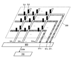
図1は、本発明の一実施形態による液晶表示装置のブロック図であって、画素の観点から示した液晶表示装置のブロック図であり、図2は、本発明の一実施形態による液晶表示装置の一つの画素に対する等価回路図である。図3は、本発明の一実施形態による液晶表示装置のブロック図であって、感知部の観点から示した液晶表示装置のブロック図であり、図4は、本発明の一実施形態による液晶表示装置の感知部に対する等価回路図であり、図5は、本発明の一実施形態による液晶表示装置の概略図である。
映像走査線G1〜Gn及び横感知データ線SY1〜SYNは、ほぼ行方向に延在しており、互いにほとんど平行であり、映像データ線D1〜Dm及び縦感知データ線SX1〜SXMは、ほぼ列方向に延在しており、互いにほとんど平行である。
図4に示す圧力感知部SUは、図面符号SLに表した横または縦感知データ線(以下、感知データ線と言う)に連結されているスイッチSWTを含む圧力感知部である。
このように、横感知データ線SY1〜SYNを通じて流れる感知データ信号を分析して接触点のY座標を判断することができ、縦感知データ線SX1〜SXMを通じて流れる感知データ信号を分析して接触点のX座標を判断することができる。
信号制御部600は、外部装置(図示せず)から入力映像信号R、G、B及びその表示を制御する入力制御信号を受信する。入力映像信号R、G、Bは、各画素PXの輝度(luminance)情報を含んでおり、輝度は決められた数、例えば、1024(=210)、256(=28)または64(=26)個の階調(gray)を有している。入力制御信号の例としては、垂直同期信号Vsync、水平同期信号Hsync、メインクロックMCLK、及びデータイネーブル信号DEなどがある。
図6は、本発明の一実施形態による薄膜トランジスタの配置図であり、図7は、図6の薄膜トランジスタ表示板を含む液晶表示装置のVIIA−VIIA線に沿った断面図であり、図8は、図6の薄膜トランジスタ表示板を含む液晶表示装置のVIIB−VIIB線に沿った断面図である。
透明なガラスまたはプラスチックなどで作られた絶縁基板110上に、複数の映像走査線(image scanning line)121、複数の横感知データ線126、及び複数の維持電極線131が形成されている。
映像走査線121、横感知データ線126、及び維持電極線131上には、窒化ケイ素(SiNx)または酸化ケイ素(SiOx)などで作られたゲート絶縁膜(gate insulating layer)140が形成されている。
半導体154とオーミックコンタクト部材163、165の側面も絶縁基板110面に対して傾斜しており、その傾斜角は30°〜80°程度である。
映像データ線171、ドレイン電極175、及び縦感知データ線174も、その側面が絶縁基板110面に対して30°〜80°程度の傾斜角で傾斜していることが好ましい。
画素電極191は、また、隣接する映像走査線121及び映像データ線171と重畳して開口率(apertureratio)を高めることができる。
コンタクト補助部材81、82は、各々コンタクトホール181、182を通じて映像走査線121の端部129及び映像データ線171の端部179と連結される。コンタクト補助部材81、82は、映像走査線121の端部129及び映像データ線171の端部179と外部装置との接着性を補完し、これらを保護する。
透明なガラスまたはプラスチックなどで作られた絶縁基板210上には共通電極270が形成されている。共通電極270は、ITO(indium tin oxide)またはIZO(indium zinc oxide)などの透明な導電体で作ることが好ましい。共通電極270には共通電圧Vcomが印加される。
柱型スペーサ320は、画素PXの間または画素PXの内に形成され、液晶表示板組立体300に均一に分布して配置されている。柱型スペーサ320は、薄膜トランジスタ表示板100と共通電極表示板200との間に間隙を作り、柱型スペーサ320の高さは薄膜トランジスタ表示板100の感知用突起184a、184bの高さより高く形成されている。
薄膜トランジスタ表示板100及び共通電極表示板200の二つの表示板は、柱型スペーサ320の代りにビーズスペーサ(beads spacer)(図示せず)などによって支持されるようにすることもできる。
このような仮想の縦及び横感知データ線を形成することで静電容量などの差による縦縞または横縞の不良などを減少させる。
図9は、図6の薄膜トランジスタ表示板を含む液晶表示装置のVIIA−VIIA線に沿った断面図の他の実施例である。
つまり、薄膜トランジスタ表示板100’は、絶縁基板110上に複数のゲート電極124を含む複数の映像走査線121、及び延長部126aを含む複数の横感知データ線126が形成されており、その上にゲート絶縁膜140、複数の島型の半導体154、複数の島型のオーミックコンタクト部材163、165が順次に形成されている。オーミックコンタクト部材163、165及びゲート絶縁膜140上には、複数のソース電極173を含む複数の映像データ線171、複数のドレイン電極175及び複数の拡張部174aを含む複数の縦感知データ線174が形成されており、その上に下部保護膜180pが形成されている。
下部及び上部保護膜180p、180qまたはゲート絶縁膜140には、複数のコンタクトホール181、182、183a、183b、187が形成されており、上部保護膜180q上には複数の画素電極191と複数のコンタクト補助部材81、82が形成されている。
図9に示すものとは異なって、画素PXの間以外にも画素PXの内に形成されるようにすることができ、不透明な導電物質からなることができる。この場合、感知用突起195a、195bは画素PXの間に形成され、画素PXの開口率に影響を与えないことが良い。
薄膜トランジスタ表示板100’及び共通電極表示板200の二つの表示板は複数の柱型スペーサ320によって支持されていて、感知用突起195a、195bと共通電極270とは一定の間隔を維持しており、その間隔は約0.001μm以上であることが良い。
本発明の実施形態においては、感知部として圧力感知部を説明したが、これに限定されず、外部から印加される圧力によって静電容量が変わる可変キャパシタを利用した感知部や、光の強さによって出力信号が変わる光センサなどを利用することもできる。また、本発明の表示装置は、二種類以上の感知部を含んで接触判断の正確度を向上させることができる。
また、本発明の実施形態においては、表示装置として液晶表示装置を説明したが、これに限定されず、プラズマ表示装置(plasma display device)、有機発光表示装置(organic light emitting display)などのような表示装置でも同一に適用できる。
81、82 コンタクト補助部材
100、100’ 薄膜トランジスタ表示板
110、210 絶縁基板
121 映像走査線
124 ゲート電極
126 横感知データ線
126a 横感知データ線の延長部
129 映像走査線の端部
131 維持電極線
137 拡張部
140 ゲート絶縁膜
154 半導体
163、165 オーミックコンタクト部材
171 映像データ線
173 ソース電極
174 縦感知データ線
174a 縦感知データ線の拡張部
175 ドレイン電極
177 ドレイン電極の拡張部
179 映像データ線の端部
180p 下部保護膜
180q 上部保護膜
181、182、183a、183b、187 コンタクトホール
184a、184b、195a、195b 感知用突起
191 画素電極
194a、194b、194a’、194b’ 導電部材
200 共通電極表示板
230 カラーフィルタ
270 共通電極
300 液晶表示板組立体
320 柱型スペーサ
400 映像走査部
500 映像データ駆動部
550 階調電圧生成部
600 信号制御部
610 単一チップ
620 FPC基板
700 接触判断部
800 感知信号処理部
Claims (29)
- 基板上に形成され、ゲート電極、ソース電極、及びドレイン電極を備える薄膜トランジスタと、
前記ソース電極及び前記ドレイン電極上に形成され、前記ドレイン電極の少なくとも一部を露出する第1コンタクトホールを備える第1保護膜と、
前記第1保護膜上に位置するカラーフィルタと、
前記第1保護膜上に形成され、少なくとも一つの感知用突起が形成されて第2コンタクトホールを備える第2保護膜と、
前記第2保護膜上に形成され、前記第1及び第2コンタクトホールを通じて前記ドレイン電極に連結される画素電極と、
前記感知用突起上に各々形成される少なくとも一つの導電部材と、を有し、
前記感知用突起は前記カラーフィルタ及び前記画素電極と同一の基板上に配置されることを特徴とする薄膜トランジスタ表示板。 - 前記導電部材は、前記画素電極と同一の材料で形成されることを特徴とする請求項1に記載の薄膜トランジスタ表示板。
- 前記導電部材は、ITOまたはIZOからなることを特徴とする請求項2に記載の薄膜トランジスタ表示板。
- 前記導電部材は、透明な導電性有機膜からなることを特徴とする請求項2に記載の薄膜トランジスタ表示板。
- 前記導電部材は、前記画素電極と同一層に形成されることを特徴とする請求項2に記載の薄膜トランジスタ表示板。
- 前記第2保護膜は、有機絶縁膜からなることを特徴とする請求項2に記載の薄膜トランジスタ表示板。
- 基板上に形成され、ゲート電極、ソース電極、及びドレイン電極を備える薄膜トランジスタと、
前記ソース電極及び前記ドレイン電極上に形成され、前記ドレイン電極の少なくとも一部を露出する第1コンタクトホールを備える第1保護膜と、
前記第1保護膜上に位置するカラーフィルタと、
前記第1保護膜上に形成され、前記第1コンタクトホールを通じて前記ドレイン電極に連結される画素電極と、
前記第1保護膜上に形成される少なくとも一つの導電部材と、
前記導電部材上に形成される少なくとも一つの感知用突起と、を有し、
前記感知用突起は前記カラーフィルタ及び前記画素電極と同一の基板上に配置されることを特徴とする薄膜トランジスタ表示板。 - 前記第1保護膜上に形成され、前記第1コンタクトホールと対応するように第2コンタクトホールが形成される第2保護膜をさらに含むことを特徴とする請求項7に記載の薄膜トランジスタ表示板。
- 前記導電部材は、前記画素電極と同一の材料で形成されることを特徴とする請求項7に記載の薄膜トランジスタ表示板。
- 前記導電部材は、ITOまたはIZOからなることを特徴とする請求項9に記載の薄膜トランジスタ表示板。
- 前記導電部材は、透明な導電性有機膜からなることを特徴とする請求項7に記載の薄膜トランジスタ表示板。
- 前記導電部材は、前記画素電極と同一層に形成されることを特徴とする請求項7に記載の薄膜トランジスタ表示板。
- 前記感知用突起は、透明な導電性有機膜からなることを特徴とする請求項7に記載の薄膜トランジスタ表示板。
- 共通電極が形成される第1表示板と、
ゲート電極、ソース電極、及びドレイン電極を備える薄膜トランジスタ、前記ソース電極及び前記ドレイン電極上に形成される第1保護膜、前記第1保護膜上に位置するカラーフィルタ、前記第1保護膜上に形成され、少なくとも一つの感知用突起が形成される第2保護膜、前記第2保護膜上に形成され、前記ドレイン電極と連結される画素電極、及び前記感知用突起上に形成される少なくとも一つの導電部材を含む第2表示板と、を有し、
前記感知用突起は前記カラーフィルタ及び前記画素電極と同一の基板上に配置されることを特徴とする表示装置。 - 前記導電部材は、前記画素電極と同一の材料で形成されることを特徴とする請求項14に記載の表示装置。
- 前記導電部材は、透明な導電性有機膜からなることを特徴とする請求項15に記載の表示装置。
- 前記導電部材は、前記画素電極と同一層に形成されることを特徴とする請求項14に記載の表示装置。
- 前記第2保護膜は、有機絶縁膜からなることを特徴とする請求項14に記載の表示装置。
- 前記第1表示板は、前記共通電極上に形成されるスペーサをさらに含むことを特徴とする請求項14に記載の表示装置。
- 前記感知用突起の高さは、前記スペーサの高さより低いことを特徴とする請求項19に記載の表示装置。
- 前記第2表示板は、前記第1保護膜上に形成されるカラ−フィルタを更に含むことを特徴とする請求項14に記載の表示装置。
- 共通電極が形成される第1表示板と、
ゲート電極、ソース電極、及びドレイン電極を備える薄膜トランジスタ、前記ソース電極及び前記ドレイン電極上に形成される第1保護膜、前記第1保護膜上に位置するカラーフィルタ、前記第1保護膜上に形成され、前記ドレイン電極と連結される画素電極、前記第1保護膜上に形成される少なくとも一つの導電部材、及び前記導電部材上に形成される少なくとも一つの感知用突起を含む第2表示板と、を有し、
前記感知用突起は前記カラーフィルタ及び前記画素電極と同一の基板上に配置されることを特徴とする表示装置。 - 前記第1保護膜に形成される第2保護膜をさらに含むことを特徴とする請求項22に記載の表示装置。
- 前記導電部材は、前記画素電極と同一の材料で形成されることを特徴とする請求項22に記載の表示装置。
- 前記導電部材は、前記画素電極と同一層に形成されることを特徴とする請求項22に記載の表示装置。
- 前記感知用突起は、透明な導電性有機膜からなることを特徴とする請求項22に記載の表示装置。
- 前記第1表示板は、前記共通電極上に形成されるスペーサをさらに含むことを特徴とする請求項22に記載の表示装置。
- 前記感知用突起の高さは、前記スペーサの高さより低いことを特徴とする請求項27に記載の表示装置。
- 前記第2表示板は、前記第1保護膜上に形成されるカラーフィルタをさらに含むことを特徴とする請求項22に記載の表示装置。
Applications Claiming Priority (2)
| Application Number | Priority Date | Filing Date | Title |
|---|---|---|---|
| KR10-2006-0015481 | 2006-02-17 | ||
| KR1020060015481A KR20070082644A (ko) | 2006-02-17 | 2006-02-17 | 박막 트랜지스터 표시판 및 표시 장치 |
Publications (2)
| Publication Number | Publication Date |
|---|---|
| JP2007220123A JP2007220123A (ja) | 2007-08-30 |
| JP5240893B2 true JP5240893B2 (ja) | 2013-07-17 |
Family
ID=38427287
Family Applications (1)
| Application Number | Title | Priority Date | Filing Date |
|---|---|---|---|
| JP2007034749A Active JP5240893B2 (ja) | 2006-02-17 | 2007-02-15 | 薄膜トランジスタ表示板及び表示装置 |
Country Status (4)
| Country | Link |
|---|---|
| US (2) | US7999264B2 (ja) |
| JP (1) | JP5240893B2 (ja) |
| KR (1) | KR20070082644A (ja) |
| CN (1) | CN101026171B (ja) |
Cited By (1)
| Publication number | Priority date | Publication date | Assignee | Title |
|---|---|---|---|---|
| CN103472612A (zh) * | 2013-09-13 | 2013-12-25 | 北京京东方光电科技有限公司 | 阵列基板制备方法、阵列基板以及液晶显示装置 |
Families Citing this family (30)
| Publication number | Priority date | Publication date | Assignee | Title |
|---|---|---|---|---|
| KR101337257B1 (ko) * | 2007-04-12 | 2013-12-05 | 삼성디스플레이 주식회사 | 표시 장치용 박막 트랜지스터 표시판 |
| JP4894768B2 (ja) * | 2008-01-28 | 2012-03-14 | ソニー株式会社 | 表示装置及び電子機器 |
| JP4894769B2 (ja) * | 2008-01-28 | 2012-03-14 | ソニー株式会社 | 表示装置及び電子機器 |
| KR101451938B1 (ko) * | 2008-03-17 | 2014-10-17 | 삼성디스플레이 주식회사 | 터치스크린 내장형 표시 패널 |
| KR101534012B1 (ko) * | 2008-05-09 | 2015-07-07 | 삼성디스플레이 주식회사 | 박막 트랜지스터 표시판, 그 제조 방법 및 액정 표시 장치 |
| TWI417766B (zh) * | 2008-05-23 | 2013-12-01 | Innolux Corp | 觸控液晶顯示裝置及其驅動方法 |
| KR101571683B1 (ko) * | 2008-12-24 | 2015-12-07 | 삼성디스플레이 주식회사 | 표시 패널 및 이의 제조 방법 |
| KR101582941B1 (ko) * | 2008-12-24 | 2016-01-08 | 삼성디스플레이 주식회사 | 유기 발광 표시 장치 및 그 제조 방법 |
| JP4730443B2 (ja) * | 2009-02-04 | 2011-07-20 | ソニー株式会社 | 表示装置 |
| JP4816738B2 (ja) * | 2009-02-05 | 2011-11-16 | ソニー株式会社 | 情報入出力装置 |
| US8531432B2 (en) | 2009-02-18 | 2013-09-10 | Sharp Kabushiki Kaisha | Touch panel with built-in display device |
| CN101825819B (zh) * | 2009-03-05 | 2013-04-17 | 宏碁股份有限公司 | 液晶显示面板及整合按键于液晶显示面板的方法 |
| WO2011027702A1 (en) * | 2009-09-04 | 2011-03-10 | Semiconductor Energy Laboratory Co., Ltd. | Light-emitting device and method for manufacturing the same |
| KR101735569B1 (ko) * | 2010-02-24 | 2017-05-25 | 삼성디스플레이 주식회사 | 터치 센서를 내장한 액정 표시 장치 |
| US20110279398A1 (en) * | 2010-05-12 | 2011-11-17 | Harald Philipp | Touch screen electrode enhancements |
| KR101274719B1 (ko) * | 2010-06-11 | 2013-06-25 | 엘지디스플레이 주식회사 | 박막트랜지스터 기판 및 그 제조 방법과 그를 가지는 평판 표시 소자 |
| KR101753802B1 (ko) * | 2010-09-20 | 2017-07-04 | 엘지디스플레이 주식회사 | 터치 스크린이 내장된 액정 표시장치와 이의 제조방법 |
| TWI792087B (zh) | 2011-05-05 | 2023-02-11 | 日商半導體能源研究所股份有限公司 | 半導體裝置及其製造方法 |
| KR101415684B1 (ko) * | 2011-07-07 | 2014-08-07 | 엘지디스플레이 주식회사 | 유기전계 발광소자용 기판 및 그 제조 방법 |
| KR101879479B1 (ko) * | 2011-09-07 | 2018-07-17 | 시냅틱스 인코포레이티드 | 비-디스플레이 업데이트 시간들 동안의 용량성 센싱 |
| TWI451179B (zh) * | 2011-11-17 | 2014-09-01 | Au Optronics Corp | 畫素結構及其製造方法 |
| US20130128206A1 (en) * | 2011-11-22 | 2013-05-23 | Semiconductor Energy Laboratory Co., Ltd. | Liquid crystal display device and method for manufacturing the same |
| KR101893111B1 (ko) * | 2012-01-04 | 2018-08-31 | 삼성디스플레이 주식회사 | 센서를 포함하는 표시 장치 |
| KR101982167B1 (ko) * | 2012-06-21 | 2019-05-27 | 삼성디스플레이 주식회사 | 액정 표시 장치 |
| CN103579219B (zh) * | 2012-07-27 | 2016-03-16 | 北京京东方光电科技有限公司 | 一种平板阵列基板、传感器及平板阵列基板的制造方法 |
| KR102080009B1 (ko) * | 2013-05-29 | 2020-04-08 | 삼성디스플레이 주식회사 | 유기 발광 표시 장치 및 그 제조방법 |
| KR20140143646A (ko) | 2013-06-07 | 2014-12-17 | 삼성디스플레이 주식회사 | 터치 센서를 포함하는 표시 장치 및 그 제조 방법 |
| KR102362092B1 (ko) * | 2017-03-31 | 2022-02-11 | 삼성디스플레이 주식회사 | 유기 발광 표시 장치 |
| CN106932943A (zh) * | 2017-04-21 | 2017-07-07 | 惠科股份有限公司 | 显示面板和显示装置 |
| CN106991990A (zh) * | 2017-05-27 | 2017-07-28 | 上海天马有机发光显示技术有限公司 | 显示面板及显示装置 |
Family Cites Families (19)
| Publication number | Priority date | Publication date | Assignee | Title |
|---|---|---|---|---|
| JPH0320817A (ja) * | 1989-06-19 | 1991-01-29 | Nippon Telegr & Teleph Corp <Ntt> | 入力表示一体型ディスプレイ装置 |
| US5847690A (en) | 1995-10-24 | 1998-12-08 | Lucent Technologies Inc. | Integrated liquid crystal display and digitizer having a black matrix layer adapted for sensing screen touch location |
| JP2001042296A (ja) | 1999-07-30 | 2001-02-16 | Sony Corp | 液晶表示装置 |
| JP2001075074A (ja) * | 1999-08-18 | 2001-03-23 | Internatl Business Mach Corp <Ibm> | タッチセンサ一体型液晶表示素子 |
| US6403980B1 (en) * | 1999-11-05 | 2002-06-11 | Samsung Electronics Co., Ltd. | Thin film transistor array panel for liquid crystal display |
| KR100350536B1 (ko) | 1999-11-08 | 2002-08-28 | 삼성에스디아이 주식회사 | 편광판을 갖는 액정 표시장치 |
| US6876355B1 (en) | 2000-05-18 | 2005-04-05 | Lg. Philips Lcd Co., Ltd. | Touch screen structure to prevent image distortion |
| JP2002189533A (ja) * | 2000-08-23 | 2002-07-05 | Semiconductor Energy Lab Co Ltd | 携帯型の電子機器 |
| JP2002149346A (ja) | 2000-11-13 | 2002-05-24 | Hitachi Ltd | タッチパネルおよび画面入力型表示装置 |
| JP2003066463A (ja) | 2001-08-28 | 2003-03-05 | Citizen Watch Co Ltd | 液晶表示素子 |
| KR100832156B1 (ko) | 2001-08-29 | 2008-05-23 | 비오이 하이디스 테크놀로지 주식회사 | 액정표시장치의 제조방법 |
| JP2003195317A (ja) | 2001-12-25 | 2003-07-09 | Matsushita Electric Ind Co Ltd | 液晶表示パネル及びその製造方法 |
| US7019734B2 (en) * | 2002-07-17 | 2006-03-28 | 3M Innovative Properties Company | Resistive touch sensor having microstructured conductive layer |
| KR100902075B1 (ko) | 2002-09-05 | 2009-06-09 | 삼성전자주식회사 | 액정 표시 패널 및 이의 제조 방법 |
| KR100640997B1 (ko) | 2002-12-24 | 2006-11-02 | 엘지.필립스 엘시디 주식회사 | 액정 표시 장치 일체형 터치 패널 |
| KR100563460B1 (ko) | 2003-02-25 | 2006-03-23 | 엘지.필립스 엘시디 주식회사 | 터치패널 일체형 액정표시장치 및 그의 구동방법 |
| US7072012B2 (en) | 2003-05-12 | 2006-07-04 | Lg.Philips Lcd Co., Ltd. | Liquid crystal display device including data line divided into first and second branch lines and method of fabricating the same |
| US7586479B2 (en) * | 2004-06-10 | 2009-09-08 | Samsung Electronics Co., Ltd. | Display device and driving method thereof |
| JP5066335B2 (ja) * | 2004-11-22 | 2012-11-07 | 三星電子株式会社 | 感知素子を内蔵した表示装置 |
-
2006
- 2006-02-17 KR KR1020060015481A patent/KR20070082644A/ko not_active Application Discontinuation
-
2007
- 2007-01-31 US US11/669,583 patent/US7999264B2/en active Active
- 2007-02-07 CN CN2007100062474A patent/CN101026171B/zh active Active
- 2007-02-15 JP JP2007034749A patent/JP5240893B2/ja active Active
-
2011
- 2011-07-06 US US13/177,104 patent/US8586989B2/en active Active
Cited By (2)
| Publication number | Priority date | Publication date | Assignee | Title |
|---|---|---|---|---|
| CN103472612A (zh) * | 2013-09-13 | 2013-12-25 | 北京京东方光电科技有限公司 | 阵列基板制备方法、阵列基板以及液晶显示装置 |
| CN103472612B (zh) * | 2013-09-13 | 2016-02-03 | 北京京东方光电科技有限公司 | 阵列基板制备方法、阵列基板以及液晶显示装置 |
Also Published As
| Publication number | Publication date |
|---|---|
| US20110266547A1 (en) | 2011-11-03 |
| US8586989B2 (en) | 2013-11-19 |
| KR20070082644A (ko) | 2007-08-22 |
| US7999264B2 (en) | 2011-08-16 |
| JP2007220123A (ja) | 2007-08-30 |
| CN101026171B (zh) | 2011-07-27 |
| CN101026171A (zh) | 2007-08-29 |
| US20070194320A1 (en) | 2007-08-23 |
Similar Documents
| Publication | Publication Date | Title |
|---|---|---|
| JP5240893B2 (ja) | 薄膜トランジスタ表示板及び表示装置 | |
| KR101142993B1 (ko) | 표시 장치 및 그의 감지부 검사 방법 | |
| JP4930876B2 (ja) | 液晶表示装置 | |
| JP5099537B2 (ja) | 表示装置 | |
| US8884921B2 (en) | Display device including touch sensor | |
| JP5066335B2 (ja) | 感知素子を内蔵した表示装置 | |
| TWI412981B (zh) | 顯示面版、顯示元件以及其觸控與近接感測方法 | |
| KR101349096B1 (ko) | 디스플레이장치 | |
| US20110310035A1 (en) | Touch sensible display device | |
| JP2007199718A (ja) | 表示装置及び液晶表示板組立体、並びに表示装置の検査方法 | |
| JP2006040289A (ja) | 感知素子を内蔵した液晶表示装置 | |
| JP2014211825A (ja) | 表示装置 | |
| WO2010029662A1 (ja) | 表示装置 | |
| CN106340530B (zh) | 显示装置 | |
| KR20060056793A (ko) | 감지 소자를 내장한 표시 장치 | |
| US9019221B2 (en) | Display device integrated with touch screen panel | |
| KR20140087481A (ko) | 인셀 타입 터치인식 액정표시장치 | |
| KR20060056633A (ko) | 감지 소자를 내장한 표시 장치 | |
| KR20060099886A (ko) | 표시 장치 | |
| KR20070050209A (ko) | 표시 장치 | |
| KR20080044632A (ko) | 액정 표시 장치 | |
| KR20230133441A (ko) | 디스플레이 일체형 터치 검출 장치 |
Legal Events
| Date | Code | Title | Description |
|---|---|---|---|
| A621 | Written request for application examination |
Free format text: JAPANESE INTERMEDIATE CODE: A621 Effective date: 20100126 |
|
| A521 | Request for written amendment filed |
Free format text: JAPANESE INTERMEDIATE CODE: A523 Effective date: 20110124 |
|
| A131 | Notification of reasons for refusal |
Free format text: JAPANESE INTERMEDIATE CODE: A131 Effective date: 20120626 |
|
| A521 | Request for written amendment filed |
Free format text: JAPANESE INTERMEDIATE CODE: A523 Effective date: 20120926 |
|
| A711 | Notification of change in applicant |
Free format text: JAPANESE INTERMEDIATE CODE: A712 Effective date: 20121213 |
|
| TRDD | Decision of grant or rejection written | ||
| A01 | Written decision to grant a patent or to grant a registration (utility model) |
Free format text: JAPANESE INTERMEDIATE CODE: A01 Effective date: 20130305 |
|
| A61 | First payment of annual fees (during grant procedure) |
Free format text: JAPANESE INTERMEDIATE CODE: A61 Effective date: 20130329 |
|
| FPAY | Renewal fee payment (event date is renewal date of database) |
Free format text: PAYMENT UNTIL: 20160412 Year of fee payment: 3 |
|
| R150 | Certificate of patent or registration of utility model |
Free format text: JAPANESE INTERMEDIATE CODE: R150 Ref document number: 5240893 Country of ref document: JP Free format text: JAPANESE INTERMEDIATE CODE: R150 |
|
| R250 | Receipt of annual fees |
Free format text: JAPANESE INTERMEDIATE CODE: R250 |
|
| R250 | Receipt of annual fees |
Free format text: JAPANESE INTERMEDIATE CODE: R250 |
|
| R250 | Receipt of annual fees |
Free format text: JAPANESE INTERMEDIATE CODE: R250 |
|
| R250 | Receipt of annual fees |
Free format text: JAPANESE INTERMEDIATE CODE: R250 |
|
| R250 | Receipt of annual fees |
Free format text: JAPANESE INTERMEDIATE CODE: R250 |
|
| R250 | Receipt of annual fees |
Free format text: JAPANESE INTERMEDIATE CODE: R250 |
|
| R250 | Receipt of annual fees |
Free format text: JAPANESE INTERMEDIATE CODE: R250 |
|
| R250 | Receipt of annual fees |
Free format text: JAPANESE INTERMEDIATE CODE: R250 |
|
| R250 | Receipt of annual fees |
Free format text: JAPANESE INTERMEDIATE CODE: R250 |