WO2010029662A1 - 表示装置 - Google Patents
表示装置 Download PDFInfo
- Publication number
- WO2010029662A1 WO2010029662A1 PCT/JP2009/002397 JP2009002397W WO2010029662A1 WO 2010029662 A1 WO2010029662 A1 WO 2010029662A1 JP 2009002397 W JP2009002397 W JP 2009002397W WO 2010029662 A1 WO2010029662 A1 WO 2010029662A1
- Authority
- WO
- WIPO (PCT)
- Prior art keywords
- substrate
- display device
- electrode
- wiring
- detection
- Prior art date
Links
Images


Classifications
-
- G—PHYSICS
- G06—COMPUTING; CALCULATING OR COUNTING
- G06F—ELECTRIC DIGITAL DATA PROCESSING
- G06F3/00—Input arrangements for transferring data to be processed into a form capable of being handled by the computer; Output arrangements for transferring data from processing unit to output unit, e.g. interface arrangements
- G06F3/01—Input arrangements or combined input and output arrangements for interaction between user and computer
- G06F3/03—Arrangements for converting the position or the displacement of a member into a coded form
- G06F3/041—Digitisers, e.g. for touch screens or touch pads, characterised by the transducing means
- G06F3/047—Digitisers, e.g. for touch screens or touch pads, characterised by the transducing means using sets of wires, e.g. crossed wires
-
- G—PHYSICS
- G02—OPTICS
- G02F—OPTICAL DEVICES OR ARRANGEMENTS FOR THE CONTROL OF LIGHT BY MODIFICATION OF THE OPTICAL PROPERTIES OF THE MEDIA OF THE ELEMENTS INVOLVED THEREIN; NON-LINEAR OPTICS; FREQUENCY-CHANGING OF LIGHT; OPTICAL LOGIC ELEMENTS; OPTICAL ANALOGUE/DIGITAL CONVERTERS
- G02F1/00—Devices or arrangements for the control of the intensity, colour, phase, polarisation or direction of light arriving from an independent light source, e.g. switching, gating or modulating; Non-linear optics
- G02F1/01—Devices or arrangements for the control of the intensity, colour, phase, polarisation or direction of light arriving from an independent light source, e.g. switching, gating or modulating; Non-linear optics for the control of the intensity, phase, polarisation or colour
- G02F1/13—Devices or arrangements for the control of the intensity, colour, phase, polarisation or direction of light arriving from an independent light source, e.g. switching, gating or modulating; Non-linear optics for the control of the intensity, phase, polarisation or colour based on liquid crystals, e.g. single liquid crystal display cells
- G02F1/133—Constructional arrangements; Operation of liquid crystal cells; Circuit arrangements
- G02F1/1333—Constructional arrangements; Manufacturing methods
- G02F1/13338—Input devices, e.g. touch panels
-
- G—PHYSICS
- G06—COMPUTING; CALCULATING OR COUNTING
- G06F—ELECTRIC DIGITAL DATA PROCESSING
- G06F3/00—Input arrangements for transferring data to be processed into a form capable of being handled by the computer; Output arrangements for transferring data from processing unit to output unit, e.g. interface arrangements
- G06F3/01—Input arrangements or combined input and output arrangements for interaction between user and computer
- G06F3/03—Arrangements for converting the position or the displacement of a member into a coded form
- G06F3/041—Digitisers, e.g. for touch screens or touch pads, characterised by the transducing means
- G06F3/0412—Digitisers structurally integrated in a display
-
- G—PHYSICS
- G02—OPTICS
- G02F—OPTICAL DEVICES OR ARRANGEMENTS FOR THE CONTROL OF LIGHT BY MODIFICATION OF THE OPTICAL PROPERTIES OF THE MEDIA OF THE ELEMENTS INVOLVED THEREIN; NON-LINEAR OPTICS; FREQUENCY-CHANGING OF LIGHT; OPTICAL LOGIC ELEMENTS; OPTICAL ANALOGUE/DIGITAL CONVERTERS
- G02F1/00—Devices or arrangements for the control of the intensity, colour, phase, polarisation or direction of light arriving from an independent light source, e.g. switching, gating or modulating; Non-linear optics
- G02F1/01—Devices or arrangements for the control of the intensity, colour, phase, polarisation or direction of light arriving from an independent light source, e.g. switching, gating or modulating; Non-linear optics for the control of the intensity, phase, polarisation or colour
- G02F1/13—Devices or arrangements for the control of the intensity, colour, phase, polarisation or direction of light arriving from an independent light source, e.g. switching, gating or modulating; Non-linear optics for the control of the intensity, phase, polarisation or colour based on liquid crystals, e.g. single liquid crystal display cells
- G02F1/133—Constructional arrangements; Operation of liquid crystal cells; Circuit arrangements
- G02F1/1333—Constructional arrangements; Manufacturing methods
- G02F1/1343—Electrodes
- G02F1/134309—Electrodes characterised by their geometrical arrangement
- G02F1/134345—Subdivided pixels, e.g. for grey scale or redundancy
Definitions
- the present invention relates to a display device that detects position information on a display screen.
- thin display devices such as liquid crystal display devices have been widely used in various devices such as personal computers, mobile phones, PDAs, and game machines.
- a display device that detects positional information on a display screen by providing a touch panel overlaid on a display panel.
- a touch panel system for example, a resistance film system and an optical system are generally known.
- a transparent conductive film is attached to both the surface of the substrate attached to the display panel and the substrate side surface of the film attached to the surface of the substrate with a slight gap. And since each said transparent conductive film contacts and the electric current flows in the position pressed with the finger
- the first touch electrode is disposed so as to overlap the gate wiring and the source wiring of the TFT substrate constituting the liquid crystal display panel, while the second touch electrode is disposed so as to overlap the black matrix of the counter substrate. It is disclosed that the first and second touch electrodes are formed in a lattice shape.
- Patent Document 2 discloses that a plurality of protrusions protruding on the counter substrate side are formed on the TFT substrate, and the surface of the protrusion is covered with an electrode. Thus, position information is detected by detecting a change in electric capacity between the electrode on the protrusion and the counter electrode, or a change in resistance of the electrode and the counter electrode.
- Patent Documents 1 and 2 have a problem that the positions of two or more points on the display screen cannot be detected simultaneously.
- the optical method a position where a finger or the like touches the display screen and is shielded from light is detected by the light sensor by disposing a light sensor on the display pixel.
- the optical sensor requires a complicated circuit in order to reliably detect the position information according to the brightness of ambient ambient light, and it is inevitable that the device cost increases.
- the aperture ratio of the pixel is significantly reduced by arranging the photosensor in the pixel.
- the present invention has been made in view of such a point, and an object of the present invention is to make it thin and capable of detecting multiple points simultaneously.
- a display device is provided between a first substrate, a second substrate disposed opposite to the first substrate, and the first substrate and the second substrate.
- a counter electrode formed on the second substrate, a plurality of pixel electrodes facing the counter electrode, and the display connected to the pixel electrode on the first substrate.
- a switching device for switching and driving the medium layer is formed for each of a plurality of pixels, and at least two or more of the pixels are formed on the first substrate and the counter electrode.
- a touch electrode that is placed in contact with the counter electrode when the second substrate is pressed and curved toward the first substrate, and is connected to the touch electrode. Detects continuity with the counter electrode And out for the element is located.
- the first substrate is provided with a first protrusion that protrudes toward the second substrate and whose surface is covered with the touch electrode.
- the second substrate is provided with a second protrusion that protrudes toward the one substrate and whose surface is covered with the counter electrode.
- the switching element is connected to a gate line and a source line extending across the gate line, and the detection element includes a first detection line extending along the gate line and the source line. A second detection wiring extending along the line may be connected.
- the switching element is connected to a gate line and a source line extending across the gate line.
- the detection element includes a first detection line extending along the gate line, and the source line. May be connected.
- the switching element is connected to a gate line and a source line extending across the gate line.
- the detection element includes the gate line and a second detection line extending along the source line. May be connected.
- the display medium layer may be a liquid crystal layer.
- the display device includes a first substrate, a second substrate disposed to face the first substrate, and a display medium layer provided between the first substrate and the second substrate.
- a counter electrode is formed on the second substrate; a plurality of pixel electrodes opposed to the counter electrode; and the display medium layer connected to the pixel electrode for switching driving the first substrate.
- the switching element is a display device formed for each of a plurality of pixels, and at least two or more of the pixels are formed when the second substrate is pressed and curved toward the first substrate.
- a pixel electrode is configured to be conductive when in contact with the counter electrode, and a detecting element connected to the pixel electrode for detecting the conduction between the pixel electrode and the counter electrode is disposed.
- the second substrate is provided with a protruding portion that protrudes toward the first substrate and whose surface is covered with the counter electrode.
- a transmission region and a reflection region are formed in each of the plurality of pixels, and the protruding portion is disposed in the reflection region.
- the switching element is connected to a gate line and a source line extending across the gate line, and the detection element includes a first detection line extending along the gate line and the source line. A second detection wiring extending along the line may be connected.
- the switching element is connected to a gate line and a source line extending across the gate line.
- the detection element includes a first detection line extending along the gate line, and the source line. May be connected.
- the switching element is connected to a gate line and a source line extending across the gate line.
- the detection element includes the gate line and a second detection line extending along the source line. May be connected.
- the display medium layer may be a liquid crystal layer.
- a display medium layer such as a liquid crystal layer disposed between the counter electrode and the pixel electrode is switched by a switching element to display an image for each pixel.
- the touch electrode and the detection element are arranged in the pixel, when the second substrate is pressed and curved toward the first substrate, the touch electrode comes into contact with the counter electrode and becomes conductive.
- the touch electrode is opposed to the counter electrode when the second substrate is pressed. It is preferable because it is easy to come into contact.
- the conduction state between the touch electrode and the counter electrode is detected by a detection element.
- the detected signal is output by the first and second detection wirings.
- the first detection wiring can also be used as a gate wiring
- the second detection wiring can also be used as a source wiring.
- the pixel electrode has the function of the touch electrode
- the second substrate is pressed and curved toward the first substrate, the pixel electrode comes into contact with the counter electrode and becomes conductive.
- the second protrusion is provided on the second substrate because the pixel electrode can easily come into contact with the counter electrode when the second substrate is pressed.
- the conduction state between the pixel electrode and the counter electrode is detected by a detection element.
- the detected signal is output by the first and second detection wirings.
- the first detection wiring can also be used as a gate wiring, and the second detection wiring can also be used as a source wiring.
- the opposing electrode contacts the pixel electrode in the reflective region when the second substrate is pressed by disposing the protruding portion in the reflective region. It is preferable because it becomes easy to do.
- the touch electrode that contacts the counter electrode when the second substrate is pressed and the detection element that detects conduction between the touch electrode and the counter electrode are arranged in at least two or more pixels. As a result, it is thin and can detect multiple points simultaneously.
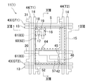
- FIG. 1 is an enlarged plan view showing pixels of the liquid crystal display device according to the first embodiment.
- FIG. 2 is a circuit diagram showing a circuit configuration corresponding to FIG. 3 is a cross-sectional view taken along line III-III in FIG. 4 is a cross-sectional view taken along line IV-IV in FIG.
- FIG. 5 is a timing chart showing the touch position detection operation.
- FIG. 6 is an enlarged plan view showing pixels of the liquid crystal display device of the second embodiment.
- FIG. 7 is a circuit diagram showing a circuit configuration corresponding to FIG.
- FIG. 8 is an enlarged plan view showing the pixels of the liquid crystal display device according to the third embodiment.
- FIG. 9 is a circuit diagram showing a circuit configuration corresponding to FIG. FIG.
- FIG. 10 is an enlarged plan view showing pixels of the liquid crystal display device according to the fourth embodiment.
- FIG. 11 is a circuit diagram showing a circuit configuration corresponding to FIG.
- FIG. 12 is an enlarged plan view showing the pixels of the liquid crystal display device according to the fifth embodiment.
- FIG. 13 is a circuit diagram showing a circuit configuration corresponding to FIG.
- FIG. 14 is an enlarged plan view showing pixels of the liquid crystal display device according to the sixth embodiment.
- FIG. 15 is a circuit diagram showing a circuit configuration corresponding to FIG.
- FIG. 16 is an enlarged plan view showing pixels of the liquid crystal display device according to the seventh embodiment.
- Embodiment 1 of the Invention 1 to 5 show Embodiment 1 of the present invention.
- FIG. 1 is a plan view showing an enlarged pixel of the liquid crystal display device according to the first embodiment.
- FIG. 2 is a circuit diagram showing a circuit configuration corresponding to FIG. 3 is a cross-sectional view taken along line III-III in FIG. 4 is a cross-sectional view taken along line IV-IV in FIG.
- a liquid crystal display device will be described as an example.
- the liquid crystal display device 1 of Embodiment 1 is configured as a transmissive liquid crystal display device that performs transmissive display.
- the liquid crystal display device 1 includes a TFT substrate 11 that is a first substrate, a counter substrate 12 that is a second substrate disposed to face the TFT substrate 11, and the counter substrate 12 and the TFT substrate. 11 and a liquid crystal layer 10 which is a display medium layer provided between the two.
- the liquid crystal display device 1 has, for example, a rectangular display area and a frame area that is a non-display area formed in a frame shape around the display area.
- the display area is composed of a plurality of pixels 5 arranged in a matrix.
- the counter substrate 12 includes, for example, a glass substrate 25 having a thickness of 0.7 mm or less, a color filter layer 26 and a counter electrode (common electrode) 27 sequentially stacked on the liquid crystal layer 10 side of the glass substrate 25. And have.
- the color filter layer 26 includes an RGB colored layer 28 and a black matrix 29 which is a light shielding film.
- the counter electrode 27 is made of, for example, ITO (Indium Tin Oxide), and is formed uniformly over the entire display area. Columnar spacers 31 for defining the thickness of the liquid crystal layer 10 (so-called cell gap) are formed on the surface of the counter electrode 27. An alignment film 30 is formed on the surface of the counter electrode 27 on the liquid crystal layer 10 side. A polarizing plate (not shown) is attached to the surface of the glass substrate 25 opposite to the liquid crystal layer 10.
- ITO Indium Tin Oxide
- the TFT substrate 11 is configured as a so-called active matrix substrate.
- the TFT substrate 11 includes a glass substrate 35 having a thickness of 0.7 mm or less, for example, and a plurality of gate wirings 13 are formed to extend in parallel to each other as shown in FIGS.
- a plurality of source lines 14 are formed on the TFT substrate 11 so as to cross the gate lines 13.
- the TFT substrate 11 is formed with a pattern of gate lines 13 and source lines 14 in a grid pattern.
- Each pixel 5 is formed by a rectangular region partitioned by the gate wiring 13 and the source wiring 14 as shown in FIGS.
- Each pixel 5 includes a plurality of pixel electrodes 15 facing the counter electrode 27 and a TFT (Thin-Film Transistor) 16 that is connected to the pixel electrode 15 and is a switching element for switching and driving the liquid crystal layer 10.
- TFT Thin-Film Transistor
- the TFT 16 is disposed, for example, in the upper left corner of the pixel 5 in FIGS. 1 and 2, and is connected to the gate electrode 17 connected to the gate wiring 13, the source electrode 18 connected to the source wiring 14, and the pixel electrode 15.
- the drain electrode 19 is provided. That is, the gate wiring 13 and the source wiring 14 are connected to the TFT 16.
- the drain electrode 19 extends to the center of the pixel 5, and a capacitor electrode 22 is formed at the tip thereof. As shown in FIG. 3, the capacitor electrode 22 is covered with an interlayer insulating film 37, and a contact hole 23 is formed in the interlayer insulating film 37 above the capacitor electrode 22. The drain electrode 19 is connected to the pixel electrode 15 via the capacitor electrode 22 and the contact hole 23.
- the signal voltage is supplied from the source wiring 14 to the pixel electrode 15 via the source electrode 18 and the drain electrode 19 in a state where the scanning voltage is applied to the gate electrode 17 via the gate wiring 13. ing.
- a plurality of capacitor wirings 20 are formed in parallel to each other so as to pass through the approximate center of each pixel.
- an insulating film 36 is interposed between the capacitor wiring 20 and the capacitor electrode 22, thereby forming a capacitor element 21 that is also called an auxiliary capacitor.
- the capacitive element 21 is formed in each pixel 5, and the display voltage in each pixel 5 is maintained substantially constant.
- the capacitor wiring 20 and the gate wiring 13 are formed on the surface of the glass substrate 35, and these are covered with an insulating film 36.
- the capacitor electrode 22 and the source wiring 14 are formed on the surface of the insulating film 36, and these are covered with an interlayer insulating film 37.
- a pixel electrode 15 is formed on the surface of the interlayer insulating film 37, and the pixel electrode 15 is covered with an alignment film 38.
- the touch electrode 41 and the detection element 42 connected to the touch electrode 41 are formed on the TFT substrate 11 for each pixel 5.
- the detection element 42 is disposed in the lower right corner of each pixel 5 in FIG. 1, for example, and is configured by a TFT.
- a first detection wiring 43 extending along the gate wiring 13 and a second detection wiring 44 extending along the source wiring 14 are connected to the detection element 42. That is, the detection element 42 includes a gate portion 45 connected to the first detection wiring 43, a source portion 46 connected to the second detection wiring 44, and a drain portion 47 formed in a substantially rectangular plate shape. have.
- the source portion 46 is covered with the interlayer insulating film 37, while the drain portion 47 is not covered with the interlayer insulating film 37.
- a first protruding portion 51 that protrudes toward the counter substrate 12 is formed on the drain portion 47.
- the first protrusion 51 is formed in a columnar shape, for example, and the surface thereof is covered with the touch electrode 41.
- the touch electrode 41 is disposed in the notch portion of the pixel electrode 15 in each pixel 5, and the surface thereof is formed at the same height as the pixel electrode 15, and faces the counter electrode 27. Has been placed.
- the detection element 42 is covered with a touch electrode 41 as shown in FIG.
- the touch electrode 41 is made of ITO and is formed in the same process as the pixel electrode 15.
- the alignment film 38 covers part of the pixel electrode 15 and the touch electrode 41, but is not formed in the vicinity of the first protrusion 51.
- the second substrate 52 is formed on the surface of the black matrix 29 on the counter substrate 12.
- the second substrate 52 is disposed at an upper position facing the first protrusion 51 and protrudes toward the TFT substrate 11.
- the second protrusion 52 is formed in a cylindrical shape made of the same material as the columnar spacer 31, and the surface thereof is covered with the counter electrode 27.
- the outer diameter of the second protrusion 52 is smaller than the outer diameter of the first protrusion 51.
- the alignment film 30 covers most of the counter electrode 27 but is not formed in the vicinity of the second protrusion 52.
- the counter electrode 27 below the second protrusion 52 comes into contact with the touch electrode 41 above the first protrusion 51 and becomes conductive. It has become.
- the detection element 42 is configured to detect conduction between the touch electrode 41 and the counter electrode 27.
- FIG. 5 is a timing chart showing the touch position detection operation.
- com in FIG. 5 means the counter electrode 27.
- an AC voltage of ⁇ 1 V is applied to the counter electrode 27.
- GT1 means the upper first detection wiring 43 in FIG. 1
- GT2 means the lower first detection wiring 43 in FIG.
- GTn means the n-th first detection wiring 43 counted from GT1.
- T2 means the second detection wiring 44 on the right side in FIG.
- the detection element 42 (GT2-T2) connected to the first detection wiring 43 of GT2 and the second detection wiring 44 of T2 will be described.
- the detection element 42 (GT1-T2) connected to the first detection wiring 43 of GT1 and the second detection wiring 44 of T2 will be described.
- the drain portion 47 and the source portion 46 of the detection element 42 are conducted and turned on as described above. Become. At this time, if the counter substrate 12 is touched and the counter electrode 27 is in contact with the touch electrode 41 connected to the detection element 42 (GT1-T2), the voltage applied to the counter electrode 27 is + or ⁇ . Current flows through the second detection wiring 44 of T2 (see symbols B and D shown in FIG. 5). By detecting this current, the touch position is detected.
- the detection element 42 (GTn-T2) connected to the first detection wiring 43 of GTn and the second detection wiring 44 of T2 will be described.
- the drain part 47 and the source part 46 of the detection element 42 are electrically connected and turned on as described above. Become. However, if the counter substrate 12 is not touched and the counter electrode 27 is not in contact with the touch electrode 41 connected to the detection element 42 (GTn-T2), the second detection wiring 44 of T2 is connected. No current flows (see symbols E and F shown in FIG. 5). Therefore, in this case, the touch position is not detected, and it is detected that there is no contact.
- the touch electrode 41 that comes into contact with the counter electrode 27 when the counter substrate 12 is pressed, and the detection element 42 that detects the conduction between the touch electrode 41 and the counter electrode 27 are provided. Since each pixel 5 is provided, the overall configuration is thin, and multiple touch positions can be detected simultaneously.
- the touch position can be detected with high accuracy with a simple configuration regardless of the brightness of ambient ambient light.
- the device cost can be reduced, and the display quality can be improved by suppressing the decrease in the aperture ratio.
- the touch electrode 41 becomes the counter electrode 27 when the counter substrate 12 is pressed. Touching can be facilitated, and the detection accuracy of the touch position can be increased.
- the display by the gate wiring 13 and the source wiring 14 is displayed in all the second detection wirings 44. Since the touch position can always be detected independently of the control, the detection accuracy can be further improved.
- Embodiment 2 of the Invention >> 6 to 7 show Embodiment 2 of the present invention.
- FIG. 6 is an enlarged plan view showing pixels of the liquid crystal display device of the second embodiment.
- FIG. 7 is a circuit diagram showing a circuit configuration corresponding to FIG. In the following embodiments, the same parts as those in FIGS. 1 to 5 are denoted by the same reference numerals, and detailed description thereof is omitted.
- the first detection wiring 43 and the second detection wiring 44 are connected to the detection element 42 separately from the gate wiring 13 and the source wiring 14 connected to the display TFT 16.
- the first detection wiring 43 is also used as the gate wiring 13.
- the gate electrode 13 of the TFT 16 and the gate portion 45 of the detection element 42 are connected to the gate wiring 13.
- the source wiring 14 is connected to the source electrode 18 of the TFT 16, while the second detection wiring 44 is connected to the source portion 46 of the detection element 42.
- Embodiment 3 of the Invention >> 8 to 9 show Embodiment 3 of the present invention.
- FIG. 8 is a plan view showing an enlarged pixel of the liquid crystal display device of the third embodiment.
- FIG. 9 is a circuit diagram showing a circuit configuration corresponding to FIG.
- the first detection wiring 43 and the second detection wiring 44 are connected to the detection element 42 separately from the gate wiring 13 and the source wiring 14 connected to the display TFT 16.
- the second detection wiring 44 is also used as the source wiring 14.
- the source electrode 18 of the TFT 16 and the source part 46 of the detection element 42 are connected to the source wiring 14.
- the gate wiring 13 is connected to the gate electrode 17 of the TFT 16, while the first detection wiring 43 is connected to the gate portion 45 of the detection element 42.
- the touch electrode 41 and the detection element 42 are provided in each pixel 5, the same effect as in the first embodiment can be obtained.
- the second detection wiring 44 is also used as the source wiring 14, the number of wirings can be reduced and the aperture ratio of the pixel 5 can be improved.
- Embodiment 4 of the Invention >> 10 to 11 show Embodiment 4 of the present invention.
- FIG. 10 is an enlarged plan view showing the pixels of the liquid crystal display device according to the fourth embodiment.
- FIG. 11 is a circuit diagram showing a circuit configuration corresponding to FIG.
- the touch electrode 41 is provided separately from the pixel electrode 15, whereas in the fourth embodiment, the pixel electrode 15 also serves as the touch electrode 41.
- the drain portion 57 is formed in a wiring shape, and the tip thereof is connected to the capacitor electrode 22. That is, both the drain part 57 of the detection element 42 and the drain electrode 19 of the TFT 16 are connected to the capacitor electrode 22.
- the pixel electrode 15 is connected to the TFT 16 and the detection element 42 via the contact hole 23 and the capacitor electrode 22, respectively.
- the first detection wiring 43 is connected to the gate portion 45, while the second detection wiring 44 is connected to the source portion 46, as in the first embodiment.
- the counter substrate 12 is provided with the second protrusion 52, but the TFT substrate 11 is not provided with the first protrusion 51.
- a part of the second projecting portion 52 is disposed so as to overlap the drain portion 47 when viewed from the normal direction of the surface of the TFT substrate 11 as shown in FIG.
- each pixel 5 is configured such that when the counter substrate 12 is pressed and curved toward the TFT substrate 11, the pixel electrode 15 contacts the counter electrode 27 and becomes conductive.
- the detection element 42 detects conduction between the pixel electrode 15 and the counter electrode 27.
- Embodiment 4- since the detection element 42 is provided in each pixel 5, the same effect as in the first embodiment can be obtained.
- the pixel electrode 15 can be formed larger by not providing the touch electrode 41, the aperture ratio can be increased and display quality can be improved.
- the display by the gate wiring 13 and the source wiring 14 is displayed in all the second detection wirings 44. Since the touch position can always be detected independently of the control, the detection accuracy can be further improved.
- Embodiment 5 of the Invention >> 12 to 13 show Embodiment 5 of the present invention.
- FIG. 12 is a plan view showing an enlarged pixel of the liquid crystal display device according to the fifth embodiment.
- FIG. 13 is a circuit diagram showing a circuit configuration corresponding to FIG.
- the first detection wiring 43 and the second detection wiring 44 are connected to the detection element 42 separately from the gate wiring 13 and the source wiring 14 connected to the display TFT 16.
- the first detection wiring 43 is also used as the gate wiring 13.
- the gate electrode 17 of the TFT 16 and the gate portion 45 of the detection element 42 are connected to the gate wiring 13.
- the source wiring 14 is connected to the source electrode 18 of the TFT 16, while the second detection wiring 44 is connected to the source portion 46 of the detection element 42.
- the detection element 42 is provided in each pixel 5 and the pixel electrode 15 also serves as the touch electrode 41, the same effect as in the fourth embodiment can be obtained.
- the first detection wiring 43 is also used as the gate wiring 13, the number of wirings can be reduced and the aperture ratio of the pixel 5 can be further improved.
- Embodiment 6 of the Invention 14 to 15 show Embodiment 6 of the present invention.
- FIG. 14 is a plan view showing an enlarged pixel of the liquid crystal display device according to the sixth embodiment.
- FIG. 15 is a circuit diagram showing a circuit configuration corresponding to FIG.
- the first detection wiring 43 and the second detection wiring 44 are connected to the detection element 42 separately from the gate wiring 13 and the source wiring 14 connected to the display TFT 16.
- the second detection wiring 44 is also used as the source wiring 14.
- the source electrode 18 of the TFT 16 and the source part 46 of the detection element 42 are connected to the source wiring 14.
- the gate wiring 13 is connected to the gate electrode 17 of the TFT 16, while the first detection wiring 43 is connected to the gate portion 45 of the detection element 42.
- the detection element 42 is provided in each pixel 5 and the pixel electrode 15 also serves as the touch electrode 41, the same effect as in the fourth embodiment can be obtained.
- the second detection wiring 44 is also used as the source wiring 14, the number of wirings can be reduced and the aperture ratio of the pixel 5 can be improved.
- Embodiment 7 of the Invention >> 16 to 18 show Embodiment 7 of the present invention.
- FIG. 16 is an enlarged plan view showing the pixels of the liquid crystal display device according to the seventh embodiment. 17 is a cross-sectional view taken along line XVII-XVII in FIG. 18 is a cross-sectional view taken along line XVIII-XVIII in FIG.
- Embodiment 7 has a semi-transmissive structure in the configuration of Embodiment 4 above. That is, in each pixel 5 in the seventh embodiment, as shown in FIGS. 16 and 18, a transmissive region 60 that transmits light and performs transmissive display, and a reflective image that reflects ambient light and performs reflective display, as shown in FIGS. A region 61 is provided.
- an interlayer insulating film 37 covering the TFT 16 and the detection element 42 is formed on the TFT substrate 11, and a transmissive region 60 is formed in the removed region 62 from which the interlayer insulating film 37 has been removed. Is formed.
- the surface of the interlayer insulating film 37 is formed in an uneven shape.
- a transparent electrode 65 made of ITO or the like as the pixel electrode 15 is formed on the side wall surface of the interlayer insulating film 37 defining the removal region 62 and on the surface of the interlayer insulating film 37.
- a reflective electrode 63 is laminated on the transparent electrode 65 covering the side wall surface of the interlayer insulating film 37 and the surrounding transparent electrode 65.
- the TFT 16, the detection element 42, and the capacitor electrode 22 are individually and independently covered with a reflective electrode 63.
- the capacitive electrode 22 has an extension part 64 extending to the transmission region 60, and the extension part 64 is connected to the transparent electrode 65.
- the drain electrode 19 of the TFT 16 is also connected to the transparent electrode 65 in the transmissive region 60.
- the pixel electrode 15 composed of the transparent electrode 65 is formed in the transmissive region 60, while the pixel electrode 15 composed of the transparent electrode 65 and the reflective electrode 63 is formed in the reflective region 61.
- a second protrusion 52 is arranged at the lower left corner in FIG. As a result, when the counter substrate 12 is touched, the counter electrode 27 below the second protrusion 52 comes into contact with the reflective electrode 63 as the pixel electrode 15.
- the touch position detection structure according to the present invention can also be applied to the transflective liquid crystal display device 1.
- the pixel electrode 15 (reflective electrode 63) is closer to the counter substrate 12 than the transmissive region 60 by the thickness of the interlayer insulating film 37, and the second protrusion 52 is provided in the reflective region 61. Since it is provided, the counter electrode 27 under the second protrusion 52 can be easily brought into contact with the pixel electrode 15 (reflection electrode 63). As a result, the detection accuracy of the touch position can be easily increased.
- the present invention may be configured as follows with respect to the first embodiment.
- the detection elements 42 are arranged in all the pixels 5, but the detection elements 42 may be arranged in at least two or more pixels 5. Further, the detection element 42 and the touch electrode 41 may be arranged on at least two or more pixels 5.
- the TFT 16 and the detection element 42 are not limited to the TFT, and other switching elements that turn on or off the current flow can also be applied.
- the present invention is not limited to this, and the same applies to the semi-transmissive structure in the other embodiments. Can do.
- the liquid crystal display device has been described as an example.
- the present invention can be similarly applied to other display devices such as an organic EL display device.
- the present invention is useful for a display device that detects position information on a display screen.
Landscapes
- Engineering & Computer Science (AREA)
- Physics & Mathematics (AREA)
- Theoretical Computer Science (AREA)
- General Engineering & Computer Science (AREA)
- General Physics & Mathematics (AREA)
- Nonlinear Science (AREA)
- Human Computer Interaction (AREA)
- Mathematical Physics (AREA)
- Chemical & Material Sciences (AREA)
- Crystallography & Structural Chemistry (AREA)
- Optics & Photonics (AREA)
- Liquid Crystal (AREA)
- Devices For Indicating Variable Information By Combining Individual Elements (AREA)
Abstract
少なくとも2つ以上の画素には、第1基板に形成されると共に対向電極に対向して配置され、第2基板が押圧されて第1基板側に湾曲した際に、対向電極に接触して導通するタッチ電極と、タッチ電極に接続されてタッチ電極と対向電極との導通を検出する検出用素子とが配置されている。
Description
本発明は、本発明は、表示画面上の位置情報を検出する表示装置に関するものである。
近年、例えば液晶表示装置等の薄型の表示装置は、パーソナルコンピュータ、携帯電話、PDA及びゲーム機器等の種々の機器に広く用いられている。また、タッチパネルが表示パネルに重ねて設けられることにより、表示画面上の位置情報を検出する表示装置も知られている。
タッチパネルの方式としては、例えば、抵抗膜方式や光学方式等が、一般に知られている。
抵抗膜方式では、表示パネルに貼り付けられた基板の表面と、当該基板の表面に僅かな隙間で貼り付けたフィルムの基板側表面との双方に、透明導電膜が貼り付けられている。そして、指やペン先等で押した位置で上記各透明導電膜が接触して電流が流れることから、その位置を検出するようになっている。
しかし、表示パネルにタッチパネルを重ねて配置する構成では、表示パネルの表面、タッチパネルの裏面、タッチパネルの内部、及びタッチパネルの表面から反射光が生じるため、表示のコントラストが低下してしまう問題がある。
また、上記各反射光が互いに干渉することによってモワレが生じる結果、表示品位が低下する問題もある。さらに、表示パネルとタッチパネルとを積層する構造上、表示装置全体が厚くなり、重くなるという問題もある。
そこで、表示パネルと抵抗膜方式のタッチパネルとを一体化することが提案されている(例えば、特許文献1及び2等参照)。
特許文献1には、液晶表示パネルを構成するTFT基板のゲート配線及びソース配線に第1タッチ電極を重ねて配置する一方、対向基板のブラックマトリクスに第2タッチ電極を重ねて配置することにより、上記第1及び第2タッチ電極を格子状に形成することが開示されている。
特許文献2には、TFT基板に対向基板側に突出する突出部を複数形成し、その突出部の表面を電極で覆うことが開示されている。そうして、突出部上の電極と対向電極との間の電気容量の変化、又は上記電極及び対向電極の抵抗の変化を検知することにより、位置情報を検出するようにしている。
ところが、上記特許文献1及び2の構成では、表示画面上の2点以上の多点の位置を同時に検出することができないという問題がある。
一方、光学方式では、表示画素に光センサを配置することにより、指等が表示画面に接触して遮光された位置を、上記光センサによって検出するようになっている。しかしながら、光センサは、周囲の外光の明暗に応じて位置情報を確実に検出するために複雑な回路が必要となり、装置コストが上昇することが避けられない。さらに、光センサを画素に配置することで、画素の開口率が大幅に低下してしまう問題がある。
本発明は、斯かる点に鑑みてなされたものであり、その目的とするところは、薄型で多点を同時に検出し得るようにすることにある。
上記の目的を達成するために、本発明に係る表示装置は、第1基板と、上記第1基板に対向して配置された第2基板と、上記第1基板及び第2基板の間に設けられた表示媒体層とを備え、上記第2基板には、対向電極が形成され、上記第1基板には、上記対向電極に対向する複数の画素電極と、該画素電極に接続されて上記表示媒体層をスイッチング駆動するためのスイッチング素子とが、複数の画素毎にそれぞれ形成された表示装置であって、少なくとも2つ以上の上記画素には、上記第1基板に形成されると共に上記対向電極に対向して配置され、上記第2基板が押圧されて上記第1基板側に湾曲した際に、上記対向電極に接触して導通するタッチ電極と、上記タッチ電極に接続されて該タッチ電極と上記対向電極との導通を検出する検出用素子とが配置されている。
上記第1基板には、上記第2基板側に突出すると共に表面が上記タッチ電極により覆われた第1突出部が設けられていることが好ましい。
上記第2基板には、上記1基板側に突出すると共に表面が上記対向電極により覆われた第2突出部が設けられていることが好ましい。
上記スイッチング素子には、ゲート配線と、該ゲート配線に交差して延びるソース配線とが接続され、上記検出用素子には、上記ゲート配線に沿って延びる第1検出用配線と、上記ソース配線に沿って延びる第2検出用配線とが接続されていてもよい。
上記スイッチング素子には、ゲート配線と、該ゲート配線に交差して延びるソース配線とが接続され、上記検出用素子には、上記ゲート配線に沿って延びる第1検出用配線と、上記ソース配線とが接続されていてもよい。
上記スイッチング素子には、ゲート配線と、該ゲート配線に交差して延びるソース配線とが接続され、上記検出用素子には、上記ゲート配線と、上記ソース配線に沿って延びる第2検出用配線とが接続されていてもよい。
上記表示媒体層は、液晶層であってもよい。
また、本発明に係る表示装置は、第1基板と、上記第1基板に対向して配置された第2基板と、上記第1基板及び第2基板の間に設けられた表示媒体層とを備え、上記第2基板には、対向電極が形成され、上記第1基板には、上記対向電極に対向する複数の画素電極と、該画素電極に接続されて上記表示媒体層をスイッチング駆動するためのスイッチング素子とが、複数の画素毎にそれぞれ形成された表示装置であって、少なくとも2つ以上の上記画素は、上記第2基板が押圧されて上記第1基板側に湾曲した際に、上記画素電極が上記対向電極に接触して導通するように構成され、上記画素電極に接続されて該画素電極と上記対向電極との導通を検出する検出用素子が配置されている。
上記第2基板には、上記1基板側に突出すると共に表面が上記対向電極により覆われた突出部が設けられていることが好ましい。
上記複数の画素には、それぞれ透過領域と反射領域とが形成され、上記突出部は、上記反射領域に配置されていることが好ましい。
上記スイッチング素子には、ゲート配線と、該ゲート配線に交差して延びるソース配線とが接続され、上記検出用素子には、上記ゲート配線に沿って延びる第1検出用配線と、上記ソース配線に沿って延びる第2検出用配線とが接続されていてもよい。
上記スイッチング素子には、ゲート配線と、該ゲート配線に交差して延びるソース配線とが接続され、上記検出用素子には、上記ゲート配線に沿って延びる第1検出用配線と、上記ソース配線とが接続されていてもよい。
上記スイッチング素子には、ゲート配線と、該ゲート配線に交差して延びるソース配線とが接続され、上記検出用素子には、上記ゲート配線と、上記ソース配線に沿って延びる第2検出用配線とが接続されていてもよい。
上記表示媒体層は、液晶層であってもよい。
-作用-
次に、本発明の作用について説明する。
次に、本発明の作用について説明する。
上記表示装置は、対向電極と画素電極との間に配置されている例えば液晶層等の表示媒体層がスイッチング素子によってスイッチング駆動されることにより、画素毎に画像の表示が行われる。
まず、画素にタッチ電極と検出用素子とが配置されている場合には、第2基板が押圧されて第1基板側に湾曲した際に、タッチ電極が対向電極に接触して導通する。
さらに、第1基板に第1突出部が設けられている場合、又は第2基板に第2突出部が設けられている場合には、第2基板が押圧された際に、タッチ電極が対向電極に接触しやすくなるために好ましい。
上記タッチ電極と対向電極との導通状態は、検出用素子によって検出される。検出された信号は、第1及び第2検出用配線によって出力される。第1検出用配線はゲート配線と兼用することが可能であり、第2検出用配線はソース配線と兼用することが可能である。
一方、画素電極が上記タッチ電極の機能を有している場合には、第2基板が押圧されて第1基板側に湾曲した際に、画素電極が対向電極に接触して導通する。
さらに、第2基板に第2突出部が設けられている場合には、第2基板が押圧された際に、画素電極が対向電極に接触しやすくなるために好ましい。
上記画素電極と対向電極との導通状態は、検出用素子によって検出される。検出された信号は、第1及び第2検出用配線によって出力される。第1検出用配線はゲート配線と兼用することが可能であり、第2検出用配線はソース配線と兼用することが可能である。
また、画素に透過領域と反射領域とが形成されている場合には、突出部を反射領域に配置することによって、第2基板が押圧された際に、対向電極が反射領域の画素電極に接触しやすくなるために好ましい。
本発明によれば、第2基板が押圧されたときに対向電極に接触するタッチ電極と、当該タッチ電極及び対向電極の導通を検出する検出用素子とを、少なくとも2つ以上の画素に配置するようにしたので、薄型で多点を同時に検出することができる。
以下、本発明の実施形態を図面に基づいて詳細に説明する。尚、本発明は、以下の実施形態に限定されるものではない。
《発明の実施形態1》
図1~図5は、本発明の実施形態1を示している。
図1~図5は、本発明の実施形態1を示している。
図1は、本実施形態1の液晶表示装置の画素を拡大して示す平面図である。図2は、図1に相当する回路構成を示す回路図である。図3は、図1におけるIII-III線断面図である。図4は、図1におけるIV-IV線断面図である。
本実施形態1では、液晶表示装置を例に挙げて説明する。本実施形態1の液晶表示装置1は、透過表示を行う透過型の液晶表示装置に構成されている。
液晶表示装置1は、図3に示すように、第1基板であるTFT基板11と、TFT基板11に対向して配置された第2基板である対向基板12と、これら対向基板12及びTFT基板11の間に設けられた表示媒体層である液晶層10とを備えている。
液晶表示装置1は、図示を省略するが、例えば矩形状の表示領域と、この表示領域の周囲に枠状に形成された非表示領域である額縁領域とを有している。上記表示領域は、マトリクス状に配置された複数の画素5によって構成されている。
対向基板12は、図3に示すように、例えば0.7mm以下の厚みのガラス基板25と、ガラス基板25の液晶層10側に順に積層されたカラーフィルタ層26及び対向電極(共通電極)27とを有している。カラーフィルタ層26には、RGBの着色層28と、遮光膜であるブラックマトリクス29とが含まれる。
対向電極27は、例えばITO(Indium Tin Oxide)により構成され、表示領域の全体に亘って一様に形成されている。対向電極27の表面には、液晶層10の厚み(所謂セルギャップ)を規定するための柱状スペーサ31が形成されている。対向電極27の液晶層10側表面には配向膜30が形成されている。また、ガラス基板25における液晶層10とは反対側の表面には、図示省略の偏光板が貼り付けられている。
一方、TFT基板11は、いわゆるアクティブマトリクス基板に構成されている。TFT基板11は、例えば0.7mm以下の厚みのガラス基板35を有し、図1及び図2に示すように、複数のゲート配線13が互いに平行に延びて形成されている。また、TFT基板11には、複数のソース配線14が上記ゲート配線13と交差して延びるように形成されている。そのことにより、TFT基板11には、ゲート配線13及びソース配線14からなる配線が格子状にパターン形成されている。
各画素5は、図1及び図2に示すように、上記ゲート配線13とソース配線14とによって区画される矩形状の領域により形成されている。各画素5には、対向電極27に対向する複数の画素電極15と、画素電極15に接続されて液晶層10をスイッチング駆動するためのスイッチング素子であるTFT(Thin-Film Transistor)16とが形成されている。
TFT16は、例えば画素5における図1及び図2で左上隅部分に配置され、ゲート配線13に接続されたゲート電極17と、ソース配線14に接続されたソース電極18と、画素電極15に接続されたドレイン電極19とを備えている。つまり、TFT16には、ゲート配線13及びソース配線14が接続されている。
ドレイン電極19は、画素5の中央まで延びており、その先端に容量電極22が形成されている。容量電極22は、図3に示すように、層間絶縁膜37によって覆われており、その層間絶縁膜37には、容量電極22の上方位置にコンタクトホール23が形成されている。そして、ドレイン電極19は、容量電極22及びコンタクトホール23を介して画素電極15に接続されている。
そうして、走査電圧がゲート配線13を介してゲート電極17に印加された状態で、信号電圧がソース配線14からソース電極18及びドレイン電極19を介して画素電極15へ供給されるようになっている。
また、TFT基板11には、複数の容量配線20が各画素の略中央を通るように、互いに平行に形成されている。容量配線20と容量電極22との間には、図3に示すように、絶縁膜36が介在されており、これらによって補助容量とも称される容量素子21が形成されている。容量素子21は、各画素5にそれぞれ形成されており、各画素5における表示電圧を略一定に維持するようになっている。
ここで、図1及び図3に示すように、ガラス基板35の表面には容量配線20及びゲート配線13が形成されており、これらは絶縁膜36によって覆われている。絶縁膜36の表面には、容量電極22及びソース配線14が形成されており、これらは層間絶縁膜37によって覆われている。層間絶縁膜37の表面には、画素電極15が形成されており、この画素電極15は、配向膜38によって覆われている。
そうして、ゲート配線13からTFT16のゲート電極17に走査信号が供給された画素5のラインでは、ソース配線14から所定の信号電圧がソース電極18及びドレイン電極19を介して画素電極15に書き込まれる。その結果、画素電極15と対向電極27との間に印加された信号電圧によって、当該画素5の液晶層10が駆動され、所望の画像が表示されるようになっている。
そして、図1及び図4に示すように、TFT基板11には、各画素5毎に、タッチ電極41と、タッチ電極41に接続された検出用素子42とがそれぞれ形成されている。
検出用素子42は、各画素5における例えば図1で右下隅部分に配置され、TFTによって構成されている。検出用素子42には、上記ゲート配線13に沿って延びる第1検出用配線43と、上記ソース配線14に沿って延びる第2検出用配線44とが接続されている。すなわち、検出用素子42は、第1検出用配線43に接続されたゲート部45と、第2検出用配線44に接続されたソース部46と、略矩形板状に形成されたドレイン部47とを有している。図4に示すように、ソース部46は層間絶縁膜37に覆われる一方、ドレイン部47は層間絶縁膜37に覆われていない。
TFT基板11には、図1及び図4に示すように、対向基板12側に突出する第1突出部51がドレイン部47上に形成されている。第1突出部51は、例えば円柱状に形成され、その表面がタッチ電極41によって覆われている。
タッチ電極41は、図1に示すように、各画素5において、画素電極15の切欠部分に配置されると共に、その表面が画素電極15と同じ高さに形成され、対向電極27に対向して配置されている。上記検出用素子42は、図1に示すように、タッチ電極41によって覆われている。また、タッチ電極41は、ITOにより構成され、画素電極15と同じ工程で形成される。
配向膜38は、画素電極15及びタッチ電極41の一部を覆っているが、第1突出部51の近傍には形成されていない。
一方、対向基板12には、上記第1突出部51に対向する上方位置に配置され、TFT基板11側に突出する第2突出部52がブラックマトリクス29の表面に形成されている。第2突出部52は、柱状スペーサ31と同じ材料からなる円柱状に形成され、その表面が対向電極27によって覆われている。この第2突出部52の外径は第1突出部51の外径よりも小さくなっている。
配向膜30は、対向電極27の大部分を覆うが、第2突出部52の近傍には形成されていない。
こうして、対向基板12が押圧されてTFT基板11側に湾曲した際に、第2突出部52下側の対向電極27が、第1突出部51上側のタッチ電極41に接触して導通するようになっている。検出用素子42は、上記タッチ電極41と対向電極27との導通を検出するように構成されている。
-タッチ位置検出方法-
次に、上記液晶表示装置1によるタッチ位置検出方法について、図5を参照して説明する。図5は、タッチ位置の検出動作を示すタイミングチャートである。
次に、上記液晶表示装置1によるタッチ位置検出方法について、図5を参照して説明する。図5は、タッチ位置の検出動作を示すタイミングチャートである。
ここで、図5のcomは対向電極27を意味する。対向電極27には、例えば±1Vの交流電圧が印加されている。
GT1は、図1で上側の第1検出用配線43を意味し、GT2は、図1で下側の第1検出用配線43を意味する。GTnは、GT1から数えてn番目の第1検出用配線43を意味する。また、T2は、図1で右側の第2検出用配線44を意味する。
まず、GT2の第1検出用配線43とT2の第2検出用配線44とに接続されている検出用素子42(GT2-T2)について説明する。
GT2の第1検出用配線43に所定の走査電圧が印加されると、当該検出用素子42(GT2-T2)のドレイン部47とソース部46とが導通してON状態になる。このとき、対向基板12がタッチされ、当該検出用素子42(GT2-T2)に接続されているタッチ電極41に対向電極27が接触していれば、対向電極27に印加されている+又は-の電圧に応じて、T2の第2検出用配線44に電流が流れる(図5に示す符号A及びC参照。)。この電流が検知されることにより、タッチ位置が検出される。
次に、GT1の第1検出用配線43とT2の第2検出用配線44とに接続されている検出用素子42(GT1-T2)について説明する。
GT1の第1検出用配線43に所定の走査電圧が印加されると、上記と同様に、当該検出用素子42(GT1-T2)のドレイン部47とソース部46とが導通してON状態になる。このとき、対向基板12がタッチされ、当該検出用素子42(GT1-T2)に接続されているタッチ電極41に対向電極27が接触していれば、対向電極27に印加されている+又は-の電圧に応じて、T2の第2検出用配線44に電流が流れる(図5に示す符号B及びD参照。)。この電流が検知されることにより、タッチ位置が検出される。
次に、GTnの第1検出用配線43とT2の第2検出用配線44とに接続されている検出用素子42(GTn-T2)について説明する。
GTnの第1検出用配線43に所定の走査電圧が印加されると、上記と同様に、当該検出用素子42(GTn-T2)のドレイン部47とソース部46とが導通してON状態になる。しかし、対向基板12がタッチされておらず、当該検出用素子42(GTn-T2)に接続されているタッチ電極41に対向電極27が接触していなければ、T2の第2検出用配線44に電流は流れない(図5に示す符号E及びF参照。)。したがって、この場合には、タッチ位置が検出されず、非接触であると検出される。
-実施形態1の効果-
したがって、この実施形態1によると、対向基板12が押圧されたときに対向電極27に接触するタッチ電極41と、当該タッチ電極41及び対向電極27の導通を検出する検出用素子42とを、各画素5にそれぞれ設けるようにしたので、全体として薄型の構成とし、多点のタッチ位置を同時に検出することができる。
したがって、この実施形態1によると、対向基板12が押圧されたときに対向電極27に接触するタッチ電極41と、当該タッチ電極41及び対向電極27の導通を検出する検出用素子42とを、各画素5にそれぞれ設けるようにしたので、全体として薄型の構成とし、多点のタッチ位置を同時に検出することができる。
さらに、複数の光センサを設けないので、周囲の外光の明暗に拘わらず、簡易な構成で高精度にタッチ位置を検出することができる。加えて、装置コストの低減を図ることができると共に、開口率の低下を抑制して表示品位の向上を図ることもできる。
さらにまた、TFT基板11に第1突出部51を設ける一方、対向基板12に第2突出部52を設けるようにしたので、対向基板12が押圧された際に、タッチ電極41を対向電極27に接触しやすくすることができ、タッチ位置の検出精度を高めることができる。
また、各検出用素子42に第1検出用配線43及び第2検出用配線44をそれぞれ接続する構成としたので、全ての第2検出用配線44において、ゲート配線13及びソース配線14による表示の制御とは独立して、常時、タッチ位置を検出できるため、検出精度をさらに高めることができる。
《発明の実施形態2》
図6~図7は、本発明の実施形態2を示している。
図6~図7は、本発明の実施形態2を示している。
図6は、本実施形態2の液晶表示装置の画素を拡大して示す平面図である。図7は、図6に相当する回路構成を示す回路図である。尚、以降の各実施形態では、図1~図5と同じ部分については同じ符号を付して、その詳細な説明を省略する。
上記実施形態1では、表示用のTFT16に接続されたゲート配線13及びソース配線14とは、別個独立に第1検出用配線43及び第2検出用配線44を検出用素子42に接続するようにしたのに対し、本実施形態2では、第1検出用配線43をゲート配線13と兼用にしたものである。
すなわち、図6及び図7に示すように、ゲート配線13には、TFT16のゲート電極17と、検出用素子42のゲート部45とが接続されている。一方、TFT16のソース電極18にはソース配線14が接続される一方、検出用素子42のソース部46には第2検出用配線44が接続されている。
そうして、表示用の走査信号がゲート配線13を介してTFT16に供給されるときに、その信号が検出用素子42のゲート部45にも供給される。このとき、対向基板12がタッチされて対向電極27にタッチ電極41が接触していれば、対向電極27に印加されている電圧に応じた電流が、当該検出用素子42から第2検出用配線44に流れる。この第2検出用配線44に流れた電流によって、タッチ位置が検出される。つまり、本実施形態2の構成によれば、各走査ラインの画素5において、表示信号の書き込みとタッチ位置の検出とが同時に行われる。
-実施形態2の効果-
したがって、この実施形態2によると、タッチ電極41及び検出用素子42を各画素5にそれぞれ設けているので、上記実施形態1と同様の効果を得ることができる。そのことに加え、第1検出用配線43をゲート配線13と兼用にしたため、配線の数を減少させて、画素5の開口率を向上させることができる。
したがって、この実施形態2によると、タッチ電極41及び検出用素子42を各画素5にそれぞれ設けているので、上記実施形態1と同様の効果を得ることができる。そのことに加え、第1検出用配線43をゲート配線13と兼用にしたため、配線の数を減少させて、画素5の開口率を向上させることができる。
《発明の実施形態3》
図8~図9は、本発明の実施形態3を示している。
図8~図9は、本発明の実施形態3を示している。
図8は、本実施形態3の液晶表示装置の画素を拡大して示す平面図である。図9は、図8に相当する回路構成を示す回路図である。
上記実施形態1では、表示用のTFT16に接続されたゲート配線13及びソース配線14とは、別個独立に第1検出用配線43及び第2検出用配線44を検出用素子42に接続するようにしたのに対し、本実施形態3では、第2検出用配線44をソース配線14と兼用にしたものである。
すなわち、図8及び図9に示すように、ソース配線14には、TFT16のソース電極18と、検出用素子42のソース部46とが接続されている。一方、TFT16のゲート電極17にはゲート配線13が接続される一方、検出用素子42のゲート部45には第1検出用配線43が接続されている。
そうして、第1検出用配線43を介して検出用素子42のゲート部45に信号電圧が供給されたときに、タッチ電極41と対向電極27とが接触していれば、対向電極27に印加されている電圧に応じた電流が、当該検出用素子42からソース配線14に流れる。このソース配線14に流れた電流によって、タッチ位置が検出される。
-実施形態3の効果-
したがって、この実施形態3によると、タッチ電極41及び検出用素子42を各画素5にそれぞれ設けているので、上記実施形態1と同様の効果を得ることができる。そのことに加え、第2検出用配線44をソース配線14と兼用にしたため、配線の数を減少させて、画素5の開口率を向上させることができる。
したがって、この実施形態3によると、タッチ電極41及び検出用素子42を各画素5にそれぞれ設けているので、上記実施形態1と同様の効果を得ることができる。そのことに加え、第2検出用配線44をソース配線14と兼用にしたため、配線の数を減少させて、画素5の開口率を向上させることができる。
《発明の実施形態4》
図10~図11は、本発明の実施形態4を示している。
図10~図11は、本発明の実施形態4を示している。
図10は、本実施形態4の液晶表示装置の画素を拡大して示す平面図である。図11は、図10に相当する回路構成を示す回路図である。
上記実施形態1では、タッチ電極41を画素電極15とは別個独立に設けたのに対し、本実施形態4は、画素電極15がタッチ電極41を兼ねるようにしたものである。
すなわち、図10及び図11に示すように、本実施形態4の検出用素子42は、ドレイン部57が配線状に形成され、その先端が容量電極22に接続されている。つまり、容量電極22には、検出用素子42のドレイン部57と、TFT16のドレイン電極19との双方が接続されている。このことにより、画素電極15には、コンタクトホール23及び容量電極22を介して、TFT16及び検出用素子42にそれぞれ接続されている。
検出用素子42には、上記実施形態1と同様に、第1検出用配線43がゲート部45に接続される一方、第2検出用配線44がソース部46に接続されている。
対向基板12には第2突出部52が設けられているが、TFT基板11には第1突出部51は設けられていない。この第2突出部52の一部は、図10に示すように、TFT基板11の表面の法線方向から見て、ドレイン部47に重なるように配置されている。
こうして、各画素5は、対向基板12が押圧されてTFT基板11側に湾曲した際に、画素電極15が対向電極27に接触して導通するように構成されている。一方、検出用素子42は、画素電極15と対向電極27との導通を検出するようになっている。
-実施形態4の効果-
したがって、この実施形態4によると、検出用素子42を各画素5にそれぞれ設けているので、上記実施形態1と同様の効果を得ることができる。そのことに加え、タッチ電極41を設けないことにより画素電極15を大きく形成することができるため、開口率を大きくして表示品位の向上を図ることができる。
したがって、この実施形態4によると、検出用素子42を各画素5にそれぞれ設けているので、上記実施形態1と同様の効果を得ることができる。そのことに加え、タッチ電極41を設けないことにより画素電極15を大きく形成することができるため、開口率を大きくして表示品位の向上を図ることができる。
さらに、各検出用素子42に第1検出用配線43及び第2検出用配線44をそれぞれ接続する構成としたので、全ての第2検出用配線44において、ゲート配線13及びソース配線14による表示の制御とは独立して、常時、タッチ位置を検出できるため、検出精度をさらに高めることができる。
《発明の実施形態5》
図12~図13は、本発明の実施形態5を示している。
図12~図13は、本発明の実施形態5を示している。
図12は、本実施形態5の液晶表示装置の画素を拡大して示す平面図である。図13は、図12に相当する回路構成を示す回路図である。
上記実施形態4では、表示用のTFT16に接続されたゲート配線13及びソース配線14とは、別個独立に第1検出用配線43及び第2検出用配線44を検出用素子42に接続するようにしたのに対し、本実施形態5では、第1検出用配線43をゲート配線13と兼用にしたものである。
すなわち、図12及び図13に示すように、ゲート配線13には、TFT16のゲート電極17と、検出用素子42のゲート部45とが接続されている。一方、TFT16のソース電極18にはソース配線14が接続される一方、検出用素子42のソース部46には第2検出用配線44が接続されている。
そうして、表示用の走査信号がゲート配線13を介してTFT16に供給されるときに、その信号が検出用素子42のゲート部45にも供給される。このとき、対向基板12がタッチされて対向電極27に画素電極15が接触していれば、対向電極27に印加されている電圧に応じた電流が、当該検出用素子42から第2検出用配線44に流れる。この第2検出用配線44に流れた電流によって、タッチ位置が検出される。つまり、本実施形態5の構成によれば、各走査ラインの画素5において、表示信号の書き込みとタッチ位置の検出とが同時に行われる。
-実施形態5の効果-
したがって、この実施形態5によると、検出用素子42を各画素5にそれぞれ設けると共に、画素電極15がタッチ電極41を兼ねるようにしたので、上記実施形態4と同様の効果を得ることができる。そのことに加え、第1検出用配線43をゲート配線13と兼用にしたため、配線の数を減少させて、画素5の開口率をさらに向上させることができる。
したがって、この実施形態5によると、検出用素子42を各画素5にそれぞれ設けると共に、画素電極15がタッチ電極41を兼ねるようにしたので、上記実施形態4と同様の効果を得ることができる。そのことに加え、第1検出用配線43をゲート配線13と兼用にしたため、配線の数を減少させて、画素5の開口率をさらに向上させることができる。
《発明の実施形態6》
図14~図15は、本発明の実施形態6を示している。
図14~図15は、本発明の実施形態6を示している。
図14は、本実施形態6の液晶表示装置の画素を拡大して示す平面図である。図15は、図14に相当する回路構成を示す回路図である。
上記実施形態4では、表示用のTFT16に接続されたゲート配線13及びソース配線14とは、別個独立に第1検出用配線43及び第2検出用配線44を検出用素子42に接続するようにしたのに対し、本実施形態6では、第2検出用配線44をソース配線14と兼用にしたものである。
すなわち、図14及び図15に示すように、ソース配線14には、TFT16のソース電極18と、検出用素子42のソース部46とが接続されている。一方、TFT16のゲート電極17にはゲート配線13が接続される一方、検出用素子42のゲート部45には第1検出用配線43が接続されている。
そうして、第1検出用配線43を介して検出用素子42のゲート部45に信号電圧が供給されたときに、画素電極15と対向電極27とが接触していれば、対向電極27に印加されている電圧に応じた電流が、当該検出用素子42からソース配線14に流れる。このソース配線14に流れた電流によって、タッチ位置が検出される。
-実施形態6の効果-
したがって、この実施形態6によると、検出用素子42を各画素5にそれぞれ設けると共に、画素電極15がタッチ電極41を兼ねるようにしたので、上記実施形態4と同様の効果を得ることができる。そのことに加え、第2検出用配線44をソース配線14と兼用にしたため、配線の数を減少させて、画素5の開口率を向上させることができる。
したがって、この実施形態6によると、検出用素子42を各画素5にそれぞれ設けると共に、画素電極15がタッチ電極41を兼ねるようにしたので、上記実施形態4と同様の効果を得ることができる。そのことに加え、第2検出用配線44をソース配線14と兼用にしたため、配線の数を減少させて、画素5の開口率を向上させることができる。
《発明の実施形態7》
図16~図18は、本発明の実施形態7を示している。
図16~図18は、本発明の実施形態7を示している。
図16は、本実施形態7の液晶表示装置の画素を拡大して示す平面図である。図17は、図16におけるXVII-XVII線断面図である。図18は、図16におけるXVIII-XVIII線断面図である。
本実施形態7は、上記実施形態4の構成において半透過構造としたものである。すなわち、本実施形態7における各画素5には、図16及び図18に示すように、光を透過して透過表示を行う透過領域60と、周囲の外光を反射して反射表示を行う反射領域61とが設けられている。
TFT基板11には、図16~図18に示すように、TFT16及び検出用素子42を覆う層間絶縁膜37が形成されると共に、層間絶縁膜37が除去された除去領域62に透過領域60が形成されている。図示は省略するが、上記層間絶縁膜37の表面は凹凸状に形成されている。
図17及び図18に示すように、除去領域62を区画している層間絶縁膜37の側壁面、及び層間絶縁膜37の表面には、画素電極15としてのITO等からなる透明電極65が形成されている。また、上記層間絶縁膜37の側壁面を覆っている透明電極65、及びその周囲の透明電極65には、反射電極63が積層されている。上記TFT16と、検出用素子42及び容量電極22とは、それぞれ別個独立に反射電極63によって覆われている。
ここで、容量電極22は、図16に示すように、透過領域60へ延びた延長部64を有し、この延長部64において透明電極65に接続されている。一方、TFT16のドレイン電極19もまた、透過領域60において透明電極65に接続されている。
こうして、透過領域60には、透明電極65からなる画素電極15が形成される一方、反射領域61には、透明電極65及び反射電極63からなる画素電極15が形成されている。
そして、各画素5の反射領域61には、図16で左下隅部分に、第2突出部52が配置されている。そのことにより、対向基板12がタッチされた際に、第2突出部52の下部の対向電極27が、画素電極15としての反射電極63に接触するようになっている。
-実施形態7の効果-
したがって、この実施形態7によると、検出用素子42を各画素5にそれぞれ設けると共に、画素電極15としての反射電極63がタッチ電極41を兼ねているので、上記実施形態4と同様の効果を得ることができる。そのことに加え、半透過型の液晶表示装置1についても、本発明に係るタッチ位置検出構造を適用することができる。
したがって、この実施形態7によると、検出用素子42を各画素5にそれぞれ設けると共に、画素電極15としての反射電極63がタッチ電極41を兼ねているので、上記実施形態4と同様の効果を得ることができる。そのことに加え、半透過型の液晶表示装置1についても、本発明に係るタッチ位置検出構造を適用することができる。
さらに、反射領域61では、透過領域60よりも、上記層間絶縁膜37の厚みだけ画素電極15(反射電極63)が対向基板12に近くなっており、その反射領域61に第2突出部52を設けるようにしたので、第2突出部52下部の対向電極27を、画素電極15(反射電極63)に容易に接触させることができる。その結果、タッチ位置の検出精度を容易に高めることができる。
《その他の実施形態》
本発明は、上記実施形態1について、以下のような構成としてもよい。
本発明は、上記実施形態1について、以下のような構成としてもよい。
上記各実施形態では、全ての画素5に検出用素子42を配置させるようにしたが、少なくとも2つ以上の画素5に、検出用素子42を配置するようにしてもよい。また、少なくとも2つ以上の画素5に、検出用素子42及びタッチ電極41を配置するようにしてもよい。
また、TFT16及び検出用素子42は、TFTに限らず電流の流れをON又はOFFする他のスイッチング素子を適用することも可能である。
また、上記実施形態7では、実施形態4において半透過構造にした例について説明したが、本発明はこれに限らず、その他の実施形態において半透過構造にしたものについても、同様に適用することができる。
また、上記各実施形態では、液晶表示装置を例に挙げて説明したが、その他に例えば有機EL表示装置等の他の表示装置についても同様に、本発明を適用することができる。
以上説明したように、本発明は、表示画面上の位置情報を検出する表示装置について有用である。
1 液晶表示装置
5 画素
10 液晶層(表示媒体層)
11 TFT基板(第1基板)
12 対向基板(第2基板)
13 ゲート配線
14 ソース配線
15 画素電極
16 TFT(スイッチング素子)
27 対向電極
41 タッチ電極
42 検出用素子
43 第1検出用配線
44 第2検出用配線
51 第1突出部
52 第2突出部
60 透過領域
61 反射領域
63 反射電極
65 透明電極
5 画素
10 液晶層(表示媒体層)
11 TFT基板(第1基板)
12 対向基板(第2基板)
13 ゲート配線
14 ソース配線
15 画素電極
16 TFT(スイッチング素子)
27 対向電極
41 タッチ電極
42 検出用素子
43 第1検出用配線
44 第2検出用配線
51 第1突出部
52 第2突出部
60 透過領域
61 反射領域
63 反射電極
65 透明電極
Claims (14)
- 第1基板と、
上記第1基板に対向して配置された第2基板と、
上記第1基板及び第2基板の間に設けられた表示媒体層とを備え、
上記第2基板には、対向電極が形成され、
上記第1基板には、上記対向電極に対向する複数の画素電極と、該画素電極に接続されて上記表示媒体層をスイッチング駆動するためのスイッチング素子とが、複数の画素毎にそれぞれ形成された表示装置であって、
少なくとも2つ以上の上記画素には、上記第1基板に形成されると共に上記対向電極に対向して配置され、上記第2基板が押圧されて上記第1基板側に湾曲した際に、上記対向電極に接触して導通するタッチ電極と、上記タッチ電極に接続されて該タッチ電極と上記対向電極との導通を検出する検出用素子とが配置されている
ことを特徴とする表示装置。 - 請求項1に記載の表示装置において、
上記第1基板には、上記第2基板側に突出すると共に表面が上記タッチ電極により覆われた第1突出部が設けられている
ことを特徴とする表示装置。 - 請求項1又は2に記載の表示装置において、
上記第2基板には、上記1基板側に突出すると共に表面が上記対向電極により覆われた第2突出部が設けられている
ことを特徴とする表示装置。 - 請求項1乃至3の何れか1つに記載の表示装置において、
上記スイッチング素子には、ゲート配線と、該ゲート配線に交差して延びるソース配線とが接続され、
上記検出用素子には、上記ゲート配線に沿って延びる第1検出用配線と、上記ソース配線に沿って延びる第2検出用配線とが接続されている
ことを特徴とする表示装置。 - 請求項1乃至3の何れか1つに記載の表示装置において、
上記スイッチング素子には、ゲート配線と、該ゲート配線に交差して延びるソース配線とが接続され、
上記検出用素子には、上記ゲート配線に沿って延びる第1検出用配線と、上記ソース配線とが接続されている
ことを特徴とする表示装置。 - 請求項1乃至3の何れか1つに記載の表示装置において、
上記スイッチング素子には、ゲート配線と、該ゲート配線に交差して延びるソース配線とが接続され、
上記検出用素子には、上記ゲート配線と、上記ソース配線に沿って延びる第2検出用配線とが接続されている
ことを特徴とする表示装置。 - 請求項1乃至6の何れか1つに記載の表示装置において、
上記表示媒体層は、液晶層である
ことを特徴とする表示装置。 - 第1基板と、
上記第1基板に対向して配置された第2基板と、
上記第1基板及び第2基板の間に設けられた表示媒体層とを備え、
上記第2基板には、対向電極が形成され、
上記第1基板には、上記対向電極に対向する複数の画素電極と、該画素電極に接続されて上記表示媒体層をスイッチング駆動するためのスイッチング素子とが、複数の画素毎にそれぞれ形成された表示装置であって、
少なくとも2つ以上の上記画素は、上記第2基板が押圧されて上記第1基板側に湾曲した際に、上記画素電極が上記対向電極に接触して導通するように構成され、上記画素電極に接続されて該画素電極と上記対向電極との導通を検出する検出用素子が配置されている
ことを特徴とする表示装置。 - 請求項8に記載の表示装置において、
上記第2基板には、上記1基板側に突出すると共に表面が上記対向電極により覆われた突出部が設けられている
ことを特徴とする表示装置。 - 請求項9に記載の表示装置において、
上記複数の画素には、それぞれ透過領域と反射領域とが形成され、
上記突出部は、上記反射領域に配置されている
ことを特徴とする表示装置。 - 請求項8乃至10の何れか1つに記載の表示装置において、
上記スイッチング素子には、ゲート配線と、該ゲート配線に交差して延びるソース配線とが接続され、
上記検出用素子には、上記ゲート配線に沿って延びる第1検出用配線と、上記ソース配線に沿って延びる第2検出用配線とが接続されている
ことを特徴とする表示装置。 - 請求項8乃至10の何れか1つに記載の表示装置において、
上記スイッチング素子には、ゲート配線と、該ゲート配線に交差して延びるソース配線とが接続され、
上記検出用素子には、上記ゲート配線に沿って延びる第1検出用配線と、上記ソース配線とが接続されている
ことを特徴とする表示装置。 - 請求項8乃至10の何れか1つに記載の表示装置において、
上記スイッチング素子には、ゲート配線と、該ゲート配線に交差して延びるソース配線とが接続され、
上記検出用素子には、上記ゲート配線と、上記ソース配線に沿って延びる第2検出用配線とが接続されている
ことを特徴とする表示装置。 - 請求項8乃至13の何れか1つに記載の表示装置において、
上記表示媒体層は、液晶層である
ことを特徴とする表示装置。
Priority Applications (1)
| Application Number | Priority Date | Filing Date | Title |
|---|---|---|---|
| US13/001,644 US8411212B2 (en) | 2008-09-09 | 2009-05-29 | Display device |
Applications Claiming Priority (2)
| Application Number | Priority Date | Filing Date | Title |
|---|---|---|---|
| JP2008230867 | 2008-09-09 | ||
| JP2008-230867 | 2008-09-09 |
Publications (1)
| Publication Number | Publication Date |
|---|---|
| WO2010029662A1 true WO2010029662A1 (ja) | 2010-03-18 |
Family
ID=42004928
Family Applications (1)
| Application Number | Title | Priority Date | Filing Date |
|---|---|---|---|
| PCT/JP2009/002397 WO2010029662A1 (ja) | 2008-09-09 | 2009-05-29 | 表示装置 |
Country Status (2)
| Country | Link |
|---|---|
| US (1) | US8411212B2 (ja) |
| WO (1) | WO2010029662A1 (ja) |
Cited By (1)
| Publication number | Priority date | Publication date | Assignee | Title |
|---|---|---|---|---|
| JP2017182146A (ja) * | 2016-03-28 | 2017-10-05 | 株式会社ジャパンディスプレイ | センサ及びセンサ付き表示装置 |
Families Citing this family (14)
| Publication number | Priority date | Publication date | Assignee | Title |
|---|---|---|---|---|
| CN102650916B (zh) | 2011-02-25 | 2014-11-26 | 乐金显示有限公司 | 集成触摸传感器的显示设备 |
| KR101450948B1 (ko) * | 2011-08-04 | 2014-10-16 | 엘지디스플레이 주식회사 | 터치센서 일체형 표시장치 |
| TWI464788B (zh) * | 2011-12-22 | 2014-12-11 | Ind Tech Res Inst | 感測元件陣列及其製作方法 |
| KR20140043971A (ko) * | 2012-10-04 | 2014-04-14 | 삼성디스플레이 주식회사 | 표시 기판, 이의 제조 방법 및 이를 포함하는 표시 패널 |
| KR20140100788A (ko) * | 2013-02-07 | 2014-08-18 | 삼성전자주식회사 | 터치 감지가 가능한 디스플레이 패널 및 이를 가지는 디스플레이장치 |
| CN104461201B (zh) * | 2014-12-11 | 2018-04-06 | 上海天马微电子有限公司 | 触控显示装置和该触控显示装置的驱动方法 |
| CN104699316B (zh) | 2015-04-01 | 2018-01-05 | 上海天马微电子有限公司 | 阵列基板、显示面板及显示装置 |
| WO2017030080A1 (ja) * | 2015-08-19 | 2017-02-23 | シャープ株式会社 | タッチパネル付き表示装置及びタッチパネル付き表示装置の製造方法 |
| JP6503275B2 (ja) * | 2015-10-09 | 2019-04-17 | 株式会社ジャパンディスプレイ | センサ及びセンサ付き表示装置 |
| TWI581169B (zh) * | 2016-04-28 | 2017-05-01 | 友達光電股份有限公司 | 雙模式電容觸控顯示面板 |
| US10430000B2 (en) * | 2016-08-05 | 2019-10-01 | Innolux Corporation | Touch display device |
| CN108663837B (zh) * | 2017-03-31 | 2021-01-22 | 京东方科技集团股份有限公司 | 触控显示单元、触控显示基板、触控显示面板及其驱动方法 |
| US11500237B2 (en) * | 2020-11-09 | 2022-11-15 | Sharp Kabushiki Kaisha | Array substrate and display device |
| JP2023064256A (ja) * | 2021-10-26 | 2023-05-11 | シャープディスプレイテクノロジー株式会社 | アクティブマトリクス基板及び表示装置 |
Citations (5)
| Publication number | Priority date | Publication date | Assignee | Title |
|---|---|---|---|---|
| JP2001075074A (ja) * | 1999-08-18 | 2001-03-23 | Internatl Business Mach Corp <Ibm> | タッチセンサ一体型液晶表示素子 |
| JP2002287660A (ja) * | 2001-03-28 | 2002-10-04 | Seiko Epson Corp | 入力機能付き表示装置および電子機器 |
| JP2006154815A (ja) * | 2004-11-22 | 2006-06-15 | Samsung Electronics Co Ltd | 感知素子を内蔵した表示装置 |
| JP2008065302A (ja) * | 2006-09-04 | 2008-03-21 | Au Optronics Corp | 液晶表示パネル及び関連の表示装置 |
| JP2008146077A (ja) * | 2006-12-08 | 2008-06-26 | Samsung Electronics Co Ltd | 液晶表示装置及びその製造方法 |
Family Cites Families (2)
| Publication number | Priority date | Publication date | Assignee | Title |
|---|---|---|---|---|
| JP2007047851A (ja) | 2005-08-05 | 2007-02-22 | Toshiba Matsushita Display Technology Co Ltd | 画像表示装置 |
| KR101385190B1 (ko) * | 2007-02-07 | 2014-04-15 | 삼성디스플레이 주식회사 | 액정 표시 패널 및 이의 제조 방법 |
-
2009
- 2009-05-29 US US13/001,644 patent/US8411212B2/en not_active Expired - Fee Related
- 2009-05-29 WO PCT/JP2009/002397 patent/WO2010029662A1/ja active Application Filing
Patent Citations (5)
| Publication number | Priority date | Publication date | Assignee | Title |
|---|---|---|---|---|
| JP2001075074A (ja) * | 1999-08-18 | 2001-03-23 | Internatl Business Mach Corp <Ibm> | タッチセンサ一体型液晶表示素子 |
| JP2002287660A (ja) * | 2001-03-28 | 2002-10-04 | Seiko Epson Corp | 入力機能付き表示装置および電子機器 |
| JP2006154815A (ja) * | 2004-11-22 | 2006-06-15 | Samsung Electronics Co Ltd | 感知素子を内蔵した表示装置 |
| JP2008065302A (ja) * | 2006-09-04 | 2008-03-21 | Au Optronics Corp | 液晶表示パネル及び関連の表示装置 |
| JP2008146077A (ja) * | 2006-12-08 | 2008-06-26 | Samsung Electronics Co Ltd | 液晶表示装置及びその製造方法 |
Cited By (2)
| Publication number | Priority date | Publication date | Assignee | Title |
|---|---|---|---|---|
| JP2017182146A (ja) * | 2016-03-28 | 2017-10-05 | 株式会社ジャパンディスプレイ | センサ及びセンサ付き表示装置 |
| US10437364B2 (en) | 2016-03-28 | 2019-10-08 | Japan Display Inc. | Sensor and sensor-equipped display device |
Also Published As
| Publication number | Publication date |
|---|---|
| US8411212B2 (en) | 2013-04-02 |
| US20110102359A1 (en) | 2011-05-05 |
Similar Documents
| Publication | Publication Date | Title |
|---|---|---|
| WO2010029662A1 (ja) | 表示装置 | |
| KR101564332B1 (ko) | 액정 표시 장치에 일체화된 터치 스크린 패널과 그 제조 방법 및 터치 센싱 방법 | |
| JP4507480B2 (ja) | 表示装置 | |
| TWI461792B (zh) | 具有內建觸控螢幕面板的液晶顯示器 | |
| JP5240893B2 (ja) | 薄膜トランジスタ表示板及び表示装置 | |
| US8416212B2 (en) | Electro-optical device and electronic apparatus | |
| KR101347291B1 (ko) | 터치 센서 내장형 평판표시패널과 이의 구동방법 및 이를포함한 평판표시장치 | |
| JP5306059B2 (ja) | タッチパネル、表示パネル、タッチパネル用基板、表示パネル用基板および表示装置 | |
| US20100194710A1 (en) | Information input device and information input/output device | |
| KR101546049B1 (ko) | 터치 디스플레이 패널 및 그 구동 방법 | |
| US20110187669A1 (en) | Liquid crystal display device and manufacting method thereof | |
| US20140313439A1 (en) | Display device | |
| US10656476B2 (en) | Liquid crystal panel | |
| KR20110137988A (ko) | 접촉 감지 기능이 있는 표시 장치 | |
| KR20080050674A (ko) | 액정 표시 장치 | |
| KR20120094342A (ko) | 터치스크린 | |
| KR101673206B1 (ko) | 셀프 커패시터 방식 인셀 터치 액정표시장치 | |
| KR20100074820A (ko) | 진동 터치 스크린 패널과 그 제조 방법 | |
| JP2014021865A (ja) | タッチパネル付液晶表示装置及びタッチパネル付液晶表示装置の製造方法 | |
| WO2016163303A1 (ja) | タッチセンサ付き液晶表示装置 | |
| KR20060056633A (ko) | 감지 소자를 내장한 표시 장치 | |
| KR100983519B1 (ko) | 터치 스크린을 내장한 액정표시장치 | |
| US10649263B2 (en) | Touch panel liquid crystal display device and method of driving the same | |
| US10571753B2 (en) | Liquid crystal panel | |
| WO2010106594A1 (ja) | 表示装置 |
Legal Events
| Date | Code | Title | Description |
|---|---|---|---|
| 121 | Ep: the epo has been informed by wipo that ep was designated in this application |
Ref document number: 09812811 Country of ref document: EP Kind code of ref document: A1 |
|
| WWE | Wipo information: entry into national phase |
Ref document number: 13001644 Country of ref document: US |
|
| NENP | Non-entry into the national phase |
Ref country code: DE |
|
| NENP | Non-entry into the national phase |
Ref country code: JP |
|
| 122 | Ep: pct application non-entry in european phase |
Ref document number: 09812811 Country of ref document: EP Kind code of ref document: A1 |