WO2010029662A1 - Dispositif d'affichage - Google Patents
Dispositif d'affichage Download PDFInfo
- Publication number
- WO2010029662A1 WO2010029662A1 PCT/JP2009/002397 JP2009002397W WO2010029662A1 WO 2010029662 A1 WO2010029662 A1 WO 2010029662A1 JP 2009002397 W JP2009002397 W JP 2009002397W WO 2010029662 A1 WO2010029662 A1 WO 2010029662A1
- Authority
- WO
- WIPO (PCT)
- Prior art keywords
- substrate
- display device
- electrode
- wiring
- detection
- Prior art date
Links
Images


Classifications
-
- G—PHYSICS
- G06—COMPUTING; CALCULATING OR COUNTING
- G06F—ELECTRIC DIGITAL DATA PROCESSING
- G06F3/00—Input arrangements for transferring data to be processed into a form capable of being handled by the computer; Output arrangements for transferring data from processing unit to output unit, e.g. interface arrangements
- G06F3/01—Input arrangements or combined input and output arrangements for interaction between user and computer
- G06F3/03—Arrangements for converting the position or the displacement of a member into a coded form
- G06F3/041—Digitisers, e.g. for touch screens or touch pads, characterised by the transducing means
- G06F3/047—Digitisers, e.g. for touch screens or touch pads, characterised by the transducing means using sets of wires, e.g. crossed wires
-
- G—PHYSICS
- G02—OPTICS
- G02F—OPTICAL DEVICES OR ARRANGEMENTS FOR THE CONTROL OF LIGHT BY MODIFICATION OF THE OPTICAL PROPERTIES OF THE MEDIA OF THE ELEMENTS INVOLVED THEREIN; NON-LINEAR OPTICS; FREQUENCY-CHANGING OF LIGHT; OPTICAL LOGIC ELEMENTS; OPTICAL ANALOGUE/DIGITAL CONVERTERS
- G02F1/00—Devices or arrangements for the control of the intensity, colour, phase, polarisation or direction of light arriving from an independent light source, e.g. switching, gating or modulating; Non-linear optics
- G02F1/01—Devices or arrangements for the control of the intensity, colour, phase, polarisation or direction of light arriving from an independent light source, e.g. switching, gating or modulating; Non-linear optics for the control of the intensity, phase, polarisation or colour
- G02F1/13—Devices or arrangements for the control of the intensity, colour, phase, polarisation or direction of light arriving from an independent light source, e.g. switching, gating or modulating; Non-linear optics for the control of the intensity, phase, polarisation or colour based on liquid crystals, e.g. single liquid crystal display cells
- G02F1/133—Constructional arrangements; Operation of liquid crystal cells; Circuit arrangements
- G02F1/1333—Constructional arrangements; Manufacturing methods
- G02F1/13338—Input devices, e.g. touch panels
-
- G—PHYSICS
- G06—COMPUTING; CALCULATING OR COUNTING
- G06F—ELECTRIC DIGITAL DATA PROCESSING
- G06F3/00—Input arrangements for transferring data to be processed into a form capable of being handled by the computer; Output arrangements for transferring data from processing unit to output unit, e.g. interface arrangements
- G06F3/01—Input arrangements or combined input and output arrangements for interaction between user and computer
- G06F3/03—Arrangements for converting the position or the displacement of a member into a coded form
- G06F3/041—Digitisers, e.g. for touch screens or touch pads, characterised by the transducing means
- G06F3/0412—Digitisers structurally integrated in a display
-
- G—PHYSICS
- G02—OPTICS
- G02F—OPTICAL DEVICES OR ARRANGEMENTS FOR THE CONTROL OF LIGHT BY MODIFICATION OF THE OPTICAL PROPERTIES OF THE MEDIA OF THE ELEMENTS INVOLVED THEREIN; NON-LINEAR OPTICS; FREQUENCY-CHANGING OF LIGHT; OPTICAL LOGIC ELEMENTS; OPTICAL ANALOGUE/DIGITAL CONVERTERS
- G02F1/00—Devices or arrangements for the control of the intensity, colour, phase, polarisation or direction of light arriving from an independent light source, e.g. switching, gating or modulating; Non-linear optics
- G02F1/01—Devices or arrangements for the control of the intensity, colour, phase, polarisation or direction of light arriving from an independent light source, e.g. switching, gating or modulating; Non-linear optics for the control of the intensity, phase, polarisation or colour
- G02F1/13—Devices or arrangements for the control of the intensity, colour, phase, polarisation or direction of light arriving from an independent light source, e.g. switching, gating or modulating; Non-linear optics for the control of the intensity, phase, polarisation or colour based on liquid crystals, e.g. single liquid crystal display cells
- G02F1/133—Constructional arrangements; Operation of liquid crystal cells; Circuit arrangements
- G02F1/1333—Constructional arrangements; Manufacturing methods
- G02F1/1343—Electrodes
- G02F1/134309—Electrodes characterised by their geometrical arrangement
- G02F1/134345—Subdivided pixels, e.g. for grey scale or redundancy
Definitions
- the present invention relates to a display device that detects position information on a display screen.
- thin display devices such as liquid crystal display devices have been widely used in various devices such as personal computers, mobile phones, PDAs, and game machines.
- a display device that detects positional information on a display screen by providing a touch panel overlaid on a display panel.
- a touch panel system for example, a resistance film system and an optical system are generally known.
- a transparent conductive film is attached to both the surface of the substrate attached to the display panel and the substrate side surface of the film attached to the surface of the substrate with a slight gap. And since each said transparent conductive film contacts and the electric current flows in the position pressed with the finger
- the first touch electrode is disposed so as to overlap the gate wiring and the source wiring of the TFT substrate constituting the liquid crystal display panel, while the second touch electrode is disposed so as to overlap the black matrix of the counter substrate. It is disclosed that the first and second touch electrodes are formed in a lattice shape.
- Patent Document 2 discloses that a plurality of protrusions protruding on the counter substrate side are formed on the TFT substrate, and the surface of the protrusion is covered with an electrode. Thus, position information is detected by detecting a change in electric capacity between the electrode on the protrusion and the counter electrode, or a change in resistance of the electrode and the counter electrode.
- Patent Documents 1 and 2 have a problem that the positions of two or more points on the display screen cannot be detected simultaneously.
- the optical method a position where a finger or the like touches the display screen and is shielded from light is detected by the light sensor by disposing a light sensor on the display pixel.
- the optical sensor requires a complicated circuit in order to reliably detect the position information according to the brightness of ambient ambient light, and it is inevitable that the device cost increases.
- the aperture ratio of the pixel is significantly reduced by arranging the photosensor in the pixel.
- the present invention has been made in view of such a point, and an object of the present invention is to make it thin and capable of detecting multiple points simultaneously.
- a display device is provided between a first substrate, a second substrate disposed opposite to the first substrate, and the first substrate and the second substrate.
- a counter electrode formed on the second substrate, a plurality of pixel electrodes facing the counter electrode, and the display connected to the pixel electrode on the first substrate.
- a switching device for switching and driving the medium layer is formed for each of a plurality of pixels, and at least two or more of the pixels are formed on the first substrate and the counter electrode.
- a touch electrode that is placed in contact with the counter electrode when the second substrate is pressed and curved toward the first substrate, and is connected to the touch electrode. Detects continuity with the counter electrode And out for the element is located.
- the first substrate is provided with a first protrusion that protrudes toward the second substrate and whose surface is covered with the touch electrode.
- the second substrate is provided with a second protrusion that protrudes toward the one substrate and whose surface is covered with the counter electrode.
- the switching element is connected to a gate line and a source line extending across the gate line, and the detection element includes a first detection line extending along the gate line and the source line. A second detection wiring extending along the line may be connected.
- the switching element is connected to a gate line and a source line extending across the gate line.
- the detection element includes a first detection line extending along the gate line, and the source line. May be connected.
- the switching element is connected to a gate line and a source line extending across the gate line.
- the detection element includes the gate line and a second detection line extending along the source line. May be connected.
- the display medium layer may be a liquid crystal layer.
- the display device includes a first substrate, a second substrate disposed to face the first substrate, and a display medium layer provided between the first substrate and the second substrate.
- a counter electrode is formed on the second substrate; a plurality of pixel electrodes opposed to the counter electrode; and the display medium layer connected to the pixel electrode for switching driving the first substrate.
- the switching element is a display device formed for each of a plurality of pixels, and at least two or more of the pixels are formed when the second substrate is pressed and curved toward the first substrate.
- a pixel electrode is configured to be conductive when in contact with the counter electrode, and a detecting element connected to the pixel electrode for detecting the conduction between the pixel electrode and the counter electrode is disposed.
- the second substrate is provided with a protruding portion that protrudes toward the first substrate and whose surface is covered with the counter electrode.
- a transmission region and a reflection region are formed in each of the plurality of pixels, and the protruding portion is disposed in the reflection region.
- the switching element is connected to a gate line and a source line extending across the gate line, and the detection element includes a first detection line extending along the gate line and the source line. A second detection wiring extending along the line may be connected.
- the switching element is connected to a gate line and a source line extending across the gate line.
- the detection element includes a first detection line extending along the gate line, and the source line. May be connected.
- the switching element is connected to a gate line and a source line extending across the gate line.
- the detection element includes the gate line and a second detection line extending along the source line. May be connected.
- the display medium layer may be a liquid crystal layer.
- a display medium layer such as a liquid crystal layer disposed between the counter electrode and the pixel electrode is switched by a switching element to display an image for each pixel.
- the touch electrode and the detection element are arranged in the pixel, when the second substrate is pressed and curved toward the first substrate, the touch electrode comes into contact with the counter electrode and becomes conductive.
- the touch electrode is opposed to the counter electrode when the second substrate is pressed. It is preferable because it is easy to come into contact.
- the conduction state between the touch electrode and the counter electrode is detected by a detection element.
- the detected signal is output by the first and second detection wirings.
- the first detection wiring can also be used as a gate wiring
- the second detection wiring can also be used as a source wiring.
- the pixel electrode has the function of the touch electrode
- the second substrate is pressed and curved toward the first substrate, the pixel electrode comes into contact with the counter electrode and becomes conductive.
- the second protrusion is provided on the second substrate because the pixel electrode can easily come into contact with the counter electrode when the second substrate is pressed.
- the conduction state between the pixel electrode and the counter electrode is detected by a detection element.
- the detected signal is output by the first and second detection wirings.
- the first detection wiring can also be used as a gate wiring, and the second detection wiring can also be used as a source wiring.
- the opposing electrode contacts the pixel electrode in the reflective region when the second substrate is pressed by disposing the protruding portion in the reflective region. It is preferable because it becomes easy to do.
- the touch electrode that contacts the counter electrode when the second substrate is pressed and the detection element that detects conduction between the touch electrode and the counter electrode are arranged in at least two or more pixels. As a result, it is thin and can detect multiple points simultaneously.
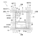
- FIG. 1 is an enlarged plan view showing pixels of the liquid crystal display device according to the first embodiment.
- FIG. 2 is a circuit diagram showing a circuit configuration corresponding to FIG. 3 is a cross-sectional view taken along line III-III in FIG. 4 is a cross-sectional view taken along line IV-IV in FIG.
- FIG. 5 is a timing chart showing the touch position detection operation.
- FIG. 6 is an enlarged plan view showing pixels of the liquid crystal display device of the second embodiment.
- FIG. 7 is a circuit diagram showing a circuit configuration corresponding to FIG.
- FIG. 8 is an enlarged plan view showing the pixels of the liquid crystal display device according to the third embodiment.
- FIG. 9 is a circuit diagram showing a circuit configuration corresponding to FIG. FIG.
- FIG. 10 is an enlarged plan view showing pixels of the liquid crystal display device according to the fourth embodiment.
- FIG. 11 is a circuit diagram showing a circuit configuration corresponding to FIG.
- FIG. 12 is an enlarged plan view showing the pixels of the liquid crystal display device according to the fifth embodiment.
- FIG. 13 is a circuit diagram showing a circuit configuration corresponding to FIG.
- FIG. 14 is an enlarged plan view showing pixels of the liquid crystal display device according to the sixth embodiment.
- FIG. 15 is a circuit diagram showing a circuit configuration corresponding to FIG.
- FIG. 16 is an enlarged plan view showing pixels of the liquid crystal display device according to the seventh embodiment.
- Embodiment 1 of the Invention 1 to 5 show Embodiment 1 of the present invention.
- FIG. 1 is a plan view showing an enlarged pixel of the liquid crystal display device according to the first embodiment.
- FIG. 2 is a circuit diagram showing a circuit configuration corresponding to FIG. 3 is a cross-sectional view taken along line III-III in FIG. 4 is a cross-sectional view taken along line IV-IV in FIG.
- a liquid crystal display device will be described as an example.
- the liquid crystal display device 1 of Embodiment 1 is configured as a transmissive liquid crystal display device that performs transmissive display.
- the liquid crystal display device 1 includes a TFT substrate 11 that is a first substrate, a counter substrate 12 that is a second substrate disposed to face the TFT substrate 11, and the counter substrate 12 and the TFT substrate. 11 and a liquid crystal layer 10 which is a display medium layer provided between the two.
- the liquid crystal display device 1 has, for example, a rectangular display area and a frame area that is a non-display area formed in a frame shape around the display area.
- the display area is composed of a plurality of pixels 5 arranged in a matrix.
- the counter substrate 12 includes, for example, a glass substrate 25 having a thickness of 0.7 mm or less, a color filter layer 26 and a counter electrode (common electrode) 27 sequentially stacked on the liquid crystal layer 10 side of the glass substrate 25. And have.
- the color filter layer 26 includes an RGB colored layer 28 and a black matrix 29 which is a light shielding film.
- the counter electrode 27 is made of, for example, ITO (Indium Tin Oxide), and is formed uniformly over the entire display area. Columnar spacers 31 for defining the thickness of the liquid crystal layer 10 (so-called cell gap) are formed on the surface of the counter electrode 27. An alignment film 30 is formed on the surface of the counter electrode 27 on the liquid crystal layer 10 side. A polarizing plate (not shown) is attached to the surface of the glass substrate 25 opposite to the liquid crystal layer 10.
- ITO Indium Tin Oxide
- the TFT substrate 11 is configured as a so-called active matrix substrate.
- the TFT substrate 11 includes a glass substrate 35 having a thickness of 0.7 mm or less, for example, and a plurality of gate wirings 13 are formed to extend in parallel to each other as shown in FIGS.
- a plurality of source lines 14 are formed on the TFT substrate 11 so as to cross the gate lines 13.
- the TFT substrate 11 is formed with a pattern of gate lines 13 and source lines 14 in a grid pattern.
- Each pixel 5 is formed by a rectangular region partitioned by the gate wiring 13 and the source wiring 14 as shown in FIGS.
- Each pixel 5 includes a plurality of pixel electrodes 15 facing the counter electrode 27 and a TFT (Thin-Film Transistor) 16 that is connected to the pixel electrode 15 and is a switching element for switching and driving the liquid crystal layer 10.
- TFT Thin-Film Transistor
- the TFT 16 is disposed, for example, in the upper left corner of the pixel 5 in FIGS. 1 and 2, and is connected to the gate electrode 17 connected to the gate wiring 13, the source electrode 18 connected to the source wiring 14, and the pixel electrode 15.
- the drain electrode 19 is provided. That is, the gate wiring 13 and the source wiring 14 are connected to the TFT 16.
- the drain electrode 19 extends to the center of the pixel 5, and a capacitor electrode 22 is formed at the tip thereof. As shown in FIG. 3, the capacitor electrode 22 is covered with an interlayer insulating film 37, and a contact hole 23 is formed in the interlayer insulating film 37 above the capacitor electrode 22. The drain electrode 19 is connected to the pixel electrode 15 via the capacitor electrode 22 and the contact hole 23.
- the signal voltage is supplied from the source wiring 14 to the pixel electrode 15 via the source electrode 18 and the drain electrode 19 in a state where the scanning voltage is applied to the gate electrode 17 via the gate wiring 13. ing.
- a plurality of capacitor wirings 20 are formed in parallel to each other so as to pass through the approximate center of each pixel.
- an insulating film 36 is interposed between the capacitor wiring 20 and the capacitor electrode 22, thereby forming a capacitor element 21 that is also called an auxiliary capacitor.
- the capacitive element 21 is formed in each pixel 5, and the display voltage in each pixel 5 is maintained substantially constant.
- the capacitor wiring 20 and the gate wiring 13 are formed on the surface of the glass substrate 35, and these are covered with an insulating film 36.
- the capacitor electrode 22 and the source wiring 14 are formed on the surface of the insulating film 36, and these are covered with an interlayer insulating film 37.
- a pixel electrode 15 is formed on the surface of the interlayer insulating film 37, and the pixel electrode 15 is covered with an alignment film 38.
- the touch electrode 41 and the detection element 42 connected to the touch electrode 41 are formed on the TFT substrate 11 for each pixel 5.
- the detection element 42 is disposed in the lower right corner of each pixel 5 in FIG. 1, for example, and is configured by a TFT.
- a first detection wiring 43 extending along the gate wiring 13 and a second detection wiring 44 extending along the source wiring 14 are connected to the detection element 42. That is, the detection element 42 includes a gate portion 45 connected to the first detection wiring 43, a source portion 46 connected to the second detection wiring 44, and a drain portion 47 formed in a substantially rectangular plate shape. have.
- the source portion 46 is covered with the interlayer insulating film 37, while the drain portion 47 is not covered with the interlayer insulating film 37.
- a first protruding portion 51 that protrudes toward the counter substrate 12 is formed on the drain portion 47.
- the first protrusion 51 is formed in a columnar shape, for example, and the surface thereof is covered with the touch electrode 41.
- the touch electrode 41 is disposed in the notch portion of the pixel electrode 15 in each pixel 5, and the surface thereof is formed at the same height as the pixel electrode 15, and faces the counter electrode 27. Has been placed.
- the detection element 42 is covered with a touch electrode 41 as shown in FIG.
- the touch electrode 41 is made of ITO and is formed in the same process as the pixel electrode 15.
- the alignment film 38 covers part of the pixel electrode 15 and the touch electrode 41, but is not formed in the vicinity of the first protrusion 51.
- the second substrate 52 is formed on the surface of the black matrix 29 on the counter substrate 12.
- the second substrate 52 is disposed at an upper position facing the first protrusion 51 and protrudes toward the TFT substrate 11.
- the second protrusion 52 is formed in a cylindrical shape made of the same material as the columnar spacer 31, and the surface thereof is covered with the counter electrode 27.
- the outer diameter of the second protrusion 52 is smaller than the outer diameter of the first protrusion 51.
- the alignment film 30 covers most of the counter electrode 27 but is not formed in the vicinity of the second protrusion 52.
- the counter electrode 27 below the second protrusion 52 comes into contact with the touch electrode 41 above the first protrusion 51 and becomes conductive. It has become.
- the detection element 42 is configured to detect conduction between the touch electrode 41 and the counter electrode 27.
- FIG. 5 is a timing chart showing the touch position detection operation.
- com in FIG. 5 means the counter electrode 27.
- an AC voltage of ⁇ 1 V is applied to the counter electrode 27.
- GT1 means the upper first detection wiring 43 in FIG. 1
- GT2 means the lower first detection wiring 43 in FIG.
- GTn means the n-th first detection wiring 43 counted from GT1.
- T2 means the second detection wiring 44 on the right side in FIG.
- the detection element 42 (GT2-T2) connected to the first detection wiring 43 of GT2 and the second detection wiring 44 of T2 will be described.
- the detection element 42 (GT1-T2) connected to the first detection wiring 43 of GT1 and the second detection wiring 44 of T2 will be described.
- the drain portion 47 and the source portion 46 of the detection element 42 are conducted and turned on as described above. Become. At this time, if the counter substrate 12 is touched and the counter electrode 27 is in contact with the touch electrode 41 connected to the detection element 42 (GT1-T2), the voltage applied to the counter electrode 27 is + or ⁇ . Current flows through the second detection wiring 44 of T2 (see symbols B and D shown in FIG. 5). By detecting this current, the touch position is detected.
- the detection element 42 (GTn-T2) connected to the first detection wiring 43 of GTn and the second detection wiring 44 of T2 will be described.
- the drain part 47 and the source part 46 of the detection element 42 are electrically connected and turned on as described above. Become. However, if the counter substrate 12 is not touched and the counter electrode 27 is not in contact with the touch electrode 41 connected to the detection element 42 (GTn-T2), the second detection wiring 44 of T2 is connected. No current flows (see symbols E and F shown in FIG. 5). Therefore, in this case, the touch position is not detected, and it is detected that there is no contact.
- the touch electrode 41 that comes into contact with the counter electrode 27 when the counter substrate 12 is pressed, and the detection element 42 that detects the conduction between the touch electrode 41 and the counter electrode 27 are provided. Since each pixel 5 is provided, the overall configuration is thin, and multiple touch positions can be detected simultaneously.
- the touch position can be detected with high accuracy with a simple configuration regardless of the brightness of ambient ambient light.
- the device cost can be reduced, and the display quality can be improved by suppressing the decrease in the aperture ratio.
- the touch electrode 41 becomes the counter electrode 27 when the counter substrate 12 is pressed. Touching can be facilitated, and the detection accuracy of the touch position can be increased.
- the display by the gate wiring 13 and the source wiring 14 is displayed in all the second detection wirings 44. Since the touch position can always be detected independently of the control, the detection accuracy can be further improved.
- Embodiment 2 of the Invention >> 6 to 7 show Embodiment 2 of the present invention.
- FIG. 6 is an enlarged plan view showing pixels of the liquid crystal display device of the second embodiment.
- FIG. 7 is a circuit diagram showing a circuit configuration corresponding to FIG. In the following embodiments, the same parts as those in FIGS. 1 to 5 are denoted by the same reference numerals, and detailed description thereof is omitted.
- the first detection wiring 43 and the second detection wiring 44 are connected to the detection element 42 separately from the gate wiring 13 and the source wiring 14 connected to the display TFT 16.
- the first detection wiring 43 is also used as the gate wiring 13.
- the gate electrode 13 of the TFT 16 and the gate portion 45 of the detection element 42 are connected to the gate wiring 13.
- the source wiring 14 is connected to the source electrode 18 of the TFT 16, while the second detection wiring 44 is connected to the source portion 46 of the detection element 42.
- Embodiment 3 of the Invention >> 8 to 9 show Embodiment 3 of the present invention.
- FIG. 8 is a plan view showing an enlarged pixel of the liquid crystal display device of the third embodiment.
- FIG. 9 is a circuit diagram showing a circuit configuration corresponding to FIG.
- the first detection wiring 43 and the second detection wiring 44 are connected to the detection element 42 separately from the gate wiring 13 and the source wiring 14 connected to the display TFT 16.
- the second detection wiring 44 is also used as the source wiring 14.
- the source electrode 18 of the TFT 16 and the source part 46 of the detection element 42 are connected to the source wiring 14.
- the gate wiring 13 is connected to the gate electrode 17 of the TFT 16, while the first detection wiring 43 is connected to the gate portion 45 of the detection element 42.
- the touch electrode 41 and the detection element 42 are provided in each pixel 5, the same effect as in the first embodiment can be obtained.
- the second detection wiring 44 is also used as the source wiring 14, the number of wirings can be reduced and the aperture ratio of the pixel 5 can be improved.
- Embodiment 4 of the Invention >> 10 to 11 show Embodiment 4 of the present invention.
- FIG. 10 is an enlarged plan view showing the pixels of the liquid crystal display device according to the fourth embodiment.
- FIG. 11 is a circuit diagram showing a circuit configuration corresponding to FIG.
- the touch electrode 41 is provided separately from the pixel electrode 15, whereas in the fourth embodiment, the pixel electrode 15 also serves as the touch electrode 41.
- the drain portion 57 is formed in a wiring shape, and the tip thereof is connected to the capacitor electrode 22. That is, both the drain part 57 of the detection element 42 and the drain electrode 19 of the TFT 16 are connected to the capacitor electrode 22.
- the pixel electrode 15 is connected to the TFT 16 and the detection element 42 via the contact hole 23 and the capacitor electrode 22, respectively.
- the first detection wiring 43 is connected to the gate portion 45, while the second detection wiring 44 is connected to the source portion 46, as in the first embodiment.
- the counter substrate 12 is provided with the second protrusion 52, but the TFT substrate 11 is not provided with the first protrusion 51.
- a part of the second projecting portion 52 is disposed so as to overlap the drain portion 47 when viewed from the normal direction of the surface of the TFT substrate 11 as shown in FIG.
- each pixel 5 is configured such that when the counter substrate 12 is pressed and curved toward the TFT substrate 11, the pixel electrode 15 contacts the counter electrode 27 and becomes conductive.
- the detection element 42 detects conduction between the pixel electrode 15 and the counter electrode 27.
- Embodiment 4- since the detection element 42 is provided in each pixel 5, the same effect as in the first embodiment can be obtained.
- the pixel electrode 15 can be formed larger by not providing the touch electrode 41, the aperture ratio can be increased and display quality can be improved.
- the display by the gate wiring 13 and the source wiring 14 is displayed in all the second detection wirings 44. Since the touch position can always be detected independently of the control, the detection accuracy can be further improved.
- Embodiment 5 of the Invention >> 12 to 13 show Embodiment 5 of the present invention.
- FIG. 12 is a plan view showing an enlarged pixel of the liquid crystal display device according to the fifth embodiment.
- FIG. 13 is a circuit diagram showing a circuit configuration corresponding to FIG.
- the first detection wiring 43 and the second detection wiring 44 are connected to the detection element 42 separately from the gate wiring 13 and the source wiring 14 connected to the display TFT 16.
- the first detection wiring 43 is also used as the gate wiring 13.
- the gate electrode 17 of the TFT 16 and the gate portion 45 of the detection element 42 are connected to the gate wiring 13.
- the source wiring 14 is connected to the source electrode 18 of the TFT 16, while the second detection wiring 44 is connected to the source portion 46 of the detection element 42.
- the detection element 42 is provided in each pixel 5 and the pixel electrode 15 also serves as the touch electrode 41, the same effect as in the fourth embodiment can be obtained.
- the first detection wiring 43 is also used as the gate wiring 13, the number of wirings can be reduced and the aperture ratio of the pixel 5 can be further improved.
- Embodiment 6 of the Invention 14 to 15 show Embodiment 6 of the present invention.
- FIG. 14 is a plan view showing an enlarged pixel of the liquid crystal display device according to the sixth embodiment.
- FIG. 15 is a circuit diagram showing a circuit configuration corresponding to FIG.
- the first detection wiring 43 and the second detection wiring 44 are connected to the detection element 42 separately from the gate wiring 13 and the source wiring 14 connected to the display TFT 16.
- the second detection wiring 44 is also used as the source wiring 14.
- the source electrode 18 of the TFT 16 and the source part 46 of the detection element 42 are connected to the source wiring 14.
- the gate wiring 13 is connected to the gate electrode 17 of the TFT 16, while the first detection wiring 43 is connected to the gate portion 45 of the detection element 42.
- the detection element 42 is provided in each pixel 5 and the pixel electrode 15 also serves as the touch electrode 41, the same effect as in the fourth embodiment can be obtained.
- the second detection wiring 44 is also used as the source wiring 14, the number of wirings can be reduced and the aperture ratio of the pixel 5 can be improved.
- Embodiment 7 of the Invention >> 16 to 18 show Embodiment 7 of the present invention.
- FIG. 16 is an enlarged plan view showing the pixels of the liquid crystal display device according to the seventh embodiment. 17 is a cross-sectional view taken along line XVII-XVII in FIG. 18 is a cross-sectional view taken along line XVIII-XVIII in FIG.
- Embodiment 7 has a semi-transmissive structure in the configuration of Embodiment 4 above. That is, in each pixel 5 in the seventh embodiment, as shown in FIGS. 16 and 18, a transmissive region 60 that transmits light and performs transmissive display, and a reflective image that reflects ambient light and performs reflective display, as shown in FIGS. A region 61 is provided.
- an interlayer insulating film 37 covering the TFT 16 and the detection element 42 is formed on the TFT substrate 11, and a transmissive region 60 is formed in the removed region 62 from which the interlayer insulating film 37 has been removed. Is formed.
- the surface of the interlayer insulating film 37 is formed in an uneven shape.
- a transparent electrode 65 made of ITO or the like as the pixel electrode 15 is formed on the side wall surface of the interlayer insulating film 37 defining the removal region 62 and on the surface of the interlayer insulating film 37.
- a reflective electrode 63 is laminated on the transparent electrode 65 covering the side wall surface of the interlayer insulating film 37 and the surrounding transparent electrode 65.
- the TFT 16, the detection element 42, and the capacitor electrode 22 are individually and independently covered with a reflective electrode 63.
- the capacitive electrode 22 has an extension part 64 extending to the transmission region 60, and the extension part 64 is connected to the transparent electrode 65.
- the drain electrode 19 of the TFT 16 is also connected to the transparent electrode 65 in the transmissive region 60.
- the pixel electrode 15 composed of the transparent electrode 65 is formed in the transmissive region 60, while the pixel electrode 15 composed of the transparent electrode 65 and the reflective electrode 63 is formed in the reflective region 61.
- a second protrusion 52 is arranged at the lower left corner in FIG. As a result, when the counter substrate 12 is touched, the counter electrode 27 below the second protrusion 52 comes into contact with the reflective electrode 63 as the pixel electrode 15.
- the touch position detection structure according to the present invention can also be applied to the transflective liquid crystal display device 1.
- the pixel electrode 15 (reflective electrode 63) is closer to the counter substrate 12 than the transmissive region 60 by the thickness of the interlayer insulating film 37, and the second protrusion 52 is provided in the reflective region 61. Since it is provided, the counter electrode 27 under the second protrusion 52 can be easily brought into contact with the pixel electrode 15 (reflection electrode 63). As a result, the detection accuracy of the touch position can be easily increased.
- the present invention may be configured as follows with respect to the first embodiment.
- the detection elements 42 are arranged in all the pixels 5, but the detection elements 42 may be arranged in at least two or more pixels 5. Further, the detection element 42 and the touch electrode 41 may be arranged on at least two or more pixels 5.
- the TFT 16 and the detection element 42 are not limited to the TFT, and other switching elements that turn on or off the current flow can also be applied.
- the present invention is not limited to this, and the same applies to the semi-transmissive structure in the other embodiments. Can do.
- the liquid crystal display device has been described as an example.
- the present invention can be similarly applied to other display devices such as an organic EL display device.
- the present invention is useful for a display device that detects position information on a display screen.
Landscapes
- Engineering & Computer Science (AREA)
- Physics & Mathematics (AREA)
- Theoretical Computer Science (AREA)
- General Engineering & Computer Science (AREA)
- General Physics & Mathematics (AREA)
- Nonlinear Science (AREA)
- Human Computer Interaction (AREA)
- Mathematical Physics (AREA)
- Chemical & Material Sciences (AREA)
- Crystallography & Structural Chemistry (AREA)
- Optics & Photonics (AREA)
- Liquid Crystal (AREA)
- Devices For Indicating Variable Information By Combining Individual Elements (AREA)
Abstract
L'invention porte sur un dispositif d'affichage ayant au moins deux pixels ou plus, dans lequel une électrode tactile et un élément de détection sont agencés. L'électrode tactile est formée dans un premier substrat et agencée de façon à faire face à une électrode opposée, de telle sorte que l'électrode tactile est mise en contact avec l'électrode opposée et électriquement couplée à celle-ci lorsqu'un second substrat est poussé et déformé vers le premier substrat. L'élément de détection est connecté à l'électrode tactile, pour ainsi détecter la conduction entre l'électrode tactile et l'électrode opposée.
Priority Applications (1)
| Application Number | Priority Date | Filing Date | Title |
|---|---|---|---|
| US13/001,644 US8411212B2 (en) | 2008-09-09 | 2009-05-29 | Display device |
Applications Claiming Priority (2)
| Application Number | Priority Date | Filing Date | Title |
|---|---|---|---|
| JP2008230867 | 2008-09-09 | ||
| JP2008-230867 | 2008-09-09 |
Publications (1)
| Publication Number | Publication Date |
|---|---|
| WO2010029662A1 true WO2010029662A1 (fr) | 2010-03-18 |
Family
ID=42004928
Family Applications (1)
| Application Number | Title | Priority Date | Filing Date |
|---|---|---|---|
| PCT/JP2009/002397 WO2010029662A1 (fr) | 2008-09-09 | 2009-05-29 | Dispositif d'affichage |
Country Status (2)
| Country | Link |
|---|---|
| US (1) | US8411212B2 (fr) |
| WO (1) | WO2010029662A1 (fr) |
Cited By (1)
| Publication number | Priority date | Publication date | Assignee | Title |
|---|---|---|---|---|
| JP2017182146A (ja) * | 2016-03-28 | 2017-10-05 | 株式会社ジャパンディスプレイ | センサ及びセンサ付き表示装置 |
Families Citing this family (14)
| Publication number | Priority date | Publication date | Assignee | Title |
|---|---|---|---|---|
| KR101450948B1 (ko) * | 2011-08-04 | 2014-10-16 | 엘지디스플레이 주식회사 | 터치센서 일체형 표시장치 |
| CN102650916B (zh) | 2011-02-25 | 2014-11-26 | 乐金显示有限公司 | 集成触摸传感器的显示设备 |
| TWI464788B (zh) * | 2011-12-22 | 2014-12-11 | Ind Tech Res Inst | 感測元件陣列及其製作方法 |
| KR20140043971A (ko) * | 2012-10-04 | 2014-04-14 | 삼성디스플레이 주식회사 | 표시 기판, 이의 제조 방법 및 이를 포함하는 표시 패널 |
| KR20140100788A (ko) * | 2013-02-07 | 2014-08-18 | 삼성전자주식회사 | 터치 감지가 가능한 디스플레이 패널 및 이를 가지는 디스플레이장치 |
| CN104461201B (zh) * | 2014-12-11 | 2018-04-06 | 上海天马微电子有限公司 | 触控显示装置和该触控显示装置的驱动方法 |
| CN104699316B (zh) * | 2015-04-01 | 2018-01-05 | 上海天马微电子有限公司 | 阵列基板、显示面板及显示装置 |
| WO2017030080A1 (fr) * | 2015-08-19 | 2017-02-23 | シャープ株式会社 | Dispositif d'affichage fixé à un panneau tactile et procédé de fabrication d'un dispositif d'affichage fixé à un panneau tactile |
| JP6503275B2 (ja) * | 2015-10-09 | 2019-04-17 | 株式会社ジャパンディスプレイ | センサ及びセンサ付き表示装置 |
| TWI581169B (zh) * | 2016-04-28 | 2017-05-01 | 友達光電股份有限公司 | 雙模式電容觸控顯示面板 |
| US10430000B2 (en) * | 2016-08-05 | 2019-10-01 | Innolux Corporation | Touch display device |
| CN108663837B (zh) * | 2017-03-31 | 2021-01-22 | 京东方科技集团股份有限公司 | 触控显示单元、触控显示基板、触控显示面板及其驱动方法 |
| US11500237B2 (en) * | 2020-11-09 | 2022-11-15 | Sharp Kabushiki Kaisha | Array substrate and display device |
| JP2023064256A (ja) * | 2021-10-26 | 2023-05-11 | シャープディスプレイテクノロジー株式会社 | アクティブマトリクス基板及び表示装置 |
Citations (5)
| Publication number | Priority date | Publication date | Assignee | Title |
|---|---|---|---|---|
| JP2001075074A (ja) * | 1999-08-18 | 2001-03-23 | Internatl Business Mach Corp <Ibm> | タッチセンサ一体型液晶表示素子 |
| JP2002287660A (ja) * | 2001-03-28 | 2002-10-04 | Seiko Epson Corp | 入力機能付き表示装置および電子機器 |
| JP2006154815A (ja) * | 2004-11-22 | 2006-06-15 | Samsung Electronics Co Ltd | 感知素子を内蔵した表示装置 |
| JP2008065302A (ja) * | 2006-09-04 | 2008-03-21 | Au Optronics Corp | 液晶表示パネル及び関連の表示装置 |
| JP2008146077A (ja) * | 2006-12-08 | 2008-06-26 | Samsung Electronics Co Ltd | 液晶表示装置及びその製造方法 |
Family Cites Families (2)
| Publication number | Priority date | Publication date | Assignee | Title |
|---|---|---|---|---|
| JP2007047851A (ja) | 2005-08-05 | 2007-02-22 | Toshiba Matsushita Display Technology Co Ltd | 画像表示装置 |
| KR101385190B1 (ko) * | 2007-02-07 | 2014-04-15 | 삼성디스플레이 주식회사 | 액정 표시 패널 및 이의 제조 방법 |
-
2009
- 2009-05-29 US US13/001,644 patent/US8411212B2/en not_active Expired - Fee Related
- 2009-05-29 WO PCT/JP2009/002397 patent/WO2010029662A1/fr active Application Filing
Patent Citations (5)
| Publication number | Priority date | Publication date | Assignee | Title |
|---|---|---|---|---|
| JP2001075074A (ja) * | 1999-08-18 | 2001-03-23 | Internatl Business Mach Corp <Ibm> | タッチセンサ一体型液晶表示素子 |
| JP2002287660A (ja) * | 2001-03-28 | 2002-10-04 | Seiko Epson Corp | 入力機能付き表示装置および電子機器 |
| JP2006154815A (ja) * | 2004-11-22 | 2006-06-15 | Samsung Electronics Co Ltd | 感知素子を内蔵した表示装置 |
| JP2008065302A (ja) * | 2006-09-04 | 2008-03-21 | Au Optronics Corp | 液晶表示パネル及び関連の表示装置 |
| JP2008146077A (ja) * | 2006-12-08 | 2008-06-26 | Samsung Electronics Co Ltd | 液晶表示装置及びその製造方法 |
Cited By (2)
| Publication number | Priority date | Publication date | Assignee | Title |
|---|---|---|---|---|
| JP2017182146A (ja) * | 2016-03-28 | 2017-10-05 | 株式会社ジャパンディスプレイ | センサ及びセンサ付き表示装置 |
| US10437364B2 (en) | 2016-03-28 | 2019-10-08 | Japan Display Inc. | Sensor and sensor-equipped display device |
Also Published As
| Publication number | Publication date |
|---|---|
| US8411212B2 (en) | 2013-04-02 |
| US20110102359A1 (en) | 2011-05-05 |
Similar Documents
| Publication | Publication Date | Title |
|---|---|---|
| WO2010029662A1 (fr) | Dispositif d'affichage | |
| KR101564332B1 (ko) | 액정 표시 장치에 일체화된 터치 스크린 패널과 그 제조 방법 및 터치 센싱 방법 | |
| JP4507480B2 (ja) | 表示装置 | |
| TWI461792B (zh) | 具有內建觸控螢幕面板的液晶顯示器 | |
| JP5240893B2 (ja) | 薄膜トランジスタ表示板及び表示装置 | |
| US8416212B2 (en) | Electro-optical device and electronic apparatus | |
| KR101347291B1 (ko) | 터치 센서 내장형 평판표시패널과 이의 구동방법 및 이를포함한 평판표시장치 | |
| JP5306059B2 (ja) | タッチパネル、表示パネル、タッチパネル用基板、表示パネル用基板および表示装置 | |
| US20100194710A1 (en) | Information input device and information input/output device | |
| KR101546049B1 (ko) | 터치 디스플레이 패널 및 그 구동 방법 | |
| US20110187669A1 (en) | Liquid crystal display device and manufacting method thereof | |
| US20140313439A1 (en) | Display device | |
| US10656476B2 (en) | Liquid crystal panel | |
| KR20110137988A (ko) | 접촉 감지 기능이 있는 표시 장치 | |
| KR20080050674A (ko) | 액정 표시 장치 | |
| KR20120094342A (ko) | 터치스크린 | |
| KR101673206B1 (ko) | 셀프 커패시터 방식 인셀 터치 액정표시장치 | |
| KR20100074820A (ko) | 진동 터치 스크린 패널과 그 제조 방법 | |
| JP2014021865A (ja) | タッチパネル付液晶表示装置及びタッチパネル付液晶表示装置の製造方法 | |
| WO2016163303A1 (fr) | Dispositif d'affichage à cristaux liquides doté d'un capteur tactile | |
| KR20060056633A (ko) | 감지 소자를 내장한 표시 장치 | |
| KR100983519B1 (ko) | 터치 스크린을 내장한 액정표시장치 | |
| US10649263B2 (en) | Touch panel liquid crystal display device and method of driving the same | |
| US10571753B2 (en) | Liquid crystal panel | |
| WO2010106594A1 (fr) | Dispositif d'affichage |
Legal Events
| Date | Code | Title | Description |
|---|---|---|---|
| 121 | Ep: the epo has been informed by wipo that ep was designated in this application |
Ref document number: 09812811 Country of ref document: EP Kind code of ref document: A1 |
|
| WWE | Wipo information: entry into national phase |
Ref document number: 13001644 Country of ref document: US |
|
| NENP | Non-entry into the national phase |
Ref country code: DE |
|
| NENP | Non-entry into the national phase |
Ref country code: JP |
|
| 122 | Ep: pct application non-entry in european phase |
Ref document number: 09812811 Country of ref document: EP Kind code of ref document: A1 |