WO2020121864A1 - ランプ制御装置 - Google Patents
ランプ制御装置 Download PDFInfo
- Publication number
- WO2020121864A1 WO2020121864A1 PCT/JP2019/046996 JP2019046996W WO2020121864A1 WO 2020121864 A1 WO2020121864 A1 WO 2020121864A1 JP 2019046996 W JP2019046996 W JP 2019046996W WO 2020121864 A1 WO2020121864 A1 WO 2020121864A1
- Authority
- WO
- WIPO (PCT)
- Prior art keywords
- lamp
- voltage
- control device
- unit
- switch
- Prior art date
- Legal status (The legal status is an assumption and is not a legal conclusion. Google has not performed a legal analysis and makes no representation as to the accuracy of the status listed.)
- Ceased
Links
Images






Classifications
-
- B—PERFORMING OPERATIONS; TRANSPORTING
- B60—VEHICLES IN GENERAL
- B60Q—ARRANGEMENT OF SIGNALLING OR LIGHTING DEVICES, THE MOUNTING OR SUPPORTING THEREOF OR CIRCUITS THEREFOR, FOR VEHICLES IN GENERAL
- B60Q11/00—Arrangement of monitoring devices for devices provided for in groups B60Q1/00 - B60Q9/00
- B60Q11/005—Arrangement of monitoring devices for devices provided for in groups B60Q1/00 - B60Q9/00 for lighting devices, e.g. indicating if lamps are burning or not
-
- B—PERFORMING OPERATIONS; TRANSPORTING
- B60—VEHICLES IN GENERAL
- B60Q—ARRANGEMENT OF SIGNALLING OR LIGHTING DEVICES, THE MOUNTING OR SUPPORTING THEREOF OR CIRCUITS THEREFOR, FOR VEHICLES IN GENERAL
- B60Q1/00—Arrangement of optical signalling or lighting devices, the mounting or supporting thereof or circuits therefor
- B60Q1/0088—Details of electrical connections
- B60Q1/0094—Arrangement of electronic circuits separated from the light source, e.g. mounting of housings for starter circuits for discharge lamps
-
- B—PERFORMING OPERATIONS; TRANSPORTING
- B60—VEHICLES IN GENERAL
- B60Q—ARRANGEMENT OF SIGNALLING OR LIGHTING DEVICES, THE MOUNTING OR SUPPORTING THEREOF OR CIRCUITS THEREFOR, FOR VEHICLES IN GENERAL
- B60Q1/00—Arrangement of optical signalling or lighting devices, the mounting or supporting thereof or circuits therefor
- B60Q1/26—Arrangement of optical signalling or lighting devices, the mounting or supporting thereof or circuits therefor the devices being primarily intended to indicate the vehicle, or parts thereof, or to give signals, to other traffic
- B60Q1/34—Arrangement of optical signalling or lighting devices, the mounting or supporting thereof or circuits therefor the devices being primarily intended to indicate the vehicle, or parts thereof, or to give signals, to other traffic for indicating change of drive direction
- B60Q1/38—Arrangement of optical signalling or lighting devices, the mounting or supporting thereof or circuits therefor the devices being primarily intended to indicate the vehicle, or parts thereof, or to give signals, to other traffic for indicating change of drive direction using immovably-mounted light sources, e.g. fixed flashing lamps
- B60Q1/382—Electronic temporisation with semiconductor amplification
-
- B—PERFORMING OPERATIONS; TRANSPORTING
- B62—LAND VEHICLES FOR TRAVELLING OTHERWISE THAN ON RAILS
- B62J—CYCLE SADDLES OR SEATS; AUXILIARY DEVICES OR ACCESSORIES SPECIALLY ADAPTED TO CYCLES AND NOT OTHERWISE PROVIDED FOR, e.g. ARTICLE CARRIERS OR CYCLE PROTECTORS
- B62J6/00—Arrangement of optical signalling or lighting devices on cycles; Mounting or supporting thereof; Circuits therefor
- B62J6/05—Direction indicators
- B62J6/055—Electrical means, e.g. lamps
- B62J6/056—Electrical means, e.g. lamps characterised by control means
-
- H—ELECTRICITY
- H05—ELECTRIC TECHNIQUES NOT OTHERWISE PROVIDED FOR
- H05B—ELECTRIC HEATING; ELECTRIC LIGHT SOURCES NOT OTHERWISE PROVIDED FOR; CIRCUIT ARRANGEMENTS FOR ELECTRIC LIGHT SOURCES, IN GENERAL
- H05B45/00—Circuit arrangements for operating light-emitting diodes [LED]
- H05B45/50—Circuit arrangements for operating light-emitting diodes [LED] responsive to malfunctions or undesirable behaviour of LEDs; responsive to LED life; Protective circuits
- H05B45/58—Circuit arrangements for operating light-emitting diodes [LED] responsive to malfunctions or undesirable behaviour of LEDs; responsive to LED life; Protective circuits involving end of life detection of LEDs
-
- Y—GENERAL TAGGING OF NEW TECHNOLOGICAL DEVELOPMENTS; GENERAL TAGGING OF CROSS-SECTIONAL TECHNOLOGIES SPANNING OVER SEVERAL SECTIONS OF THE IPC; TECHNICAL SUBJECTS COVERED BY FORMER USPC CROSS-REFERENCE ART COLLECTIONS [XRACs] AND DIGESTS
- Y02—TECHNOLOGIES OR APPLICATIONS FOR MITIGATION OR ADAPTATION AGAINST CLIMATE CHANGE
- Y02B—CLIMATE CHANGE MITIGATION TECHNOLOGIES RELATED TO BUILDINGS, e.g. HOUSING, HOUSE APPLIANCES OR RELATED END-USER APPLICATIONS
- Y02B20/00—Energy efficient lighting technologies, e.g. halogen lamps or gas discharge lamps
- Y02B20/40—Control techniques providing energy savings, e.g. smart controller or presence detection
Definitions
- the present invention relates to lighting control of a lamp (for example, a flasher lamp for a motorcycle) provided in a vehicle.
- a lamp for example, a flasher lamp for a motorcycle
- a lamp control device that controls the lighting of the flasher lamp installed in the vehicle controls the lighting of the flasher lamp according to the state of the flasher switch operated by the driver.
- the flasher switch provided on motorcycles is used in an environment exposed to rain and wind. Therefore, the flasher switch provided on the motorcycle is much more likely to flow a leak current due to raindrops, dust, etc., even when the flasher switch provided on the four-wheeled vehicle is in the off state, compared to the flasher switch provided on the four-wheeled vehicle. ..
- a lamp control device for controlling the lighting of a flasher lamp provided in a motorcycle, in particular, to prevent erroneous lighting of the lamp due to leak current.
- the lamp control device proposed in Patent Document 1 stops blinking the lamp when detecting that the current flowing through the flasher switch is a leakage current, and causes the lamp to erroneously light due to the leakage current. Suppress.
- the lamp lighting system according to the second embodiment disclosed in Patent Document 1 has a configuration in which a resistor is connected in parallel to the lamp. With this configuration, for example, even if the forward voltage Vf of the LED used as the lamp, the power supply voltage supplied to the lamp control device, and the like vary, it is possible to suppress the error in the current flowing through the flasher switch. As a result, the detection accuracy of the resistance value of the flasher switch can be improved.
- the current flowing through the flasher switch is the threshold voltage of the digital transistor provided in the input section and the Zener voltage of the Zener diode provided in the level adjusting section is the leak current. Affects the decision whether or not That is, in the lamp control device proposed in Patent Document 1, erroneous lighting of the lamp due to a leak current is accurately suppressed due to variations in the threshold voltage of the digital transistor and variations in the Zener voltage of the Zener diode. I can't.
- a second object of the present invention is to provide a lamp control device capable of accurately suppressing erroneous lighting of a lamp due to a leak current.
- a lamp control device configured to be connectable to a lamp via a first input terminal, a second input terminal, and an external switch, and a drive current for the lamp.
- An internal switch provided on a first path connecting the first input terminal and the output terminal, and a constant switch provided on a second path connecting the second input terminal and the output terminal.
- a configuration (first configuration) including a current unit, a voltage monitoring unit that monitors a voltage applied to the output terminal, and a control unit that controls the internal switch based on a monitoring result of the voltage monitoring unit. ..
- the control unit starts alternate switching between the first control mode and the second control mode when the voltage applied to the output terminal is smaller than a first predetermined value.
- the configuration (second configuration) may be adopted.
- the control unit starts the alternate switching between the first control mode and the second control mode, and then a voltage applied to the output terminal is a second predetermined value.
- the configuration may be such that the alternate switching between the first control mode and the second control mode is terminated and the control mode is fixed to the first control mode (third configuration).
- the second predetermined value may be larger than the first predetermined value (fourth configuration).
- control unit may have a configuration (fifth configuration) that PWM-drives the internal switch in the second control mode.
- control unit may have a configuration (sixth configuration) that causes the constant current unit to intermittently operate in the first control mode.
- control unit may be configured to stop the operation of the constant current unit in the second control mode (seventh configuration). ..
- a lamp system according to an aspect of the invention disclosed in this specification includes a lamp control device having any one of the first to seventh configurations, the external switch, and the lamp (eighth aspect). Is the configuration).
- a first resistor and a second resistor are provided, an input voltage is applied to one end of the first resistor and one end of the second resistor, and the other end of the first resistor is A configuration in which the second resistor is connected to the first input terminal, the other end of the second resistor is connected to the second input terminal, and the resistance value of the second resistor is larger than the resistance value of the first resistor (ninth configuration).
- a vehicle according to an aspect of the invention disclosed in this specification includes a lamp system having the eighth or ninth configuration described above, and a battery serving as a power source of the lamp system (tenth configuration). Is.
- the vehicle may be a motorcycle
- the switch may be a flasher switch
- the lamp may be a flasher lamp (eleventh configuration).
- a lamp control device for outputting a drive current of a lamp, a comparator, and a voltage applied to a first input terminal of the comparator
- a first setting unit that sets a second voltage that depends on the voltage or a third voltage that depends on the first current, the output terminal being connected to a second input terminal of the comparator, and the output terminal being The output terminal is configured to be connectable to the lamp via a switch, the output terminal is configured to be connectable to a second setting section including the switch, and the first setting section is applied to the first input terminal of the comparator.
- the second voltage is set to the second voltage
- the second setting unit sets the voltage applied to the output terminal to a fourth voltage that depends on the first voltage and the resistance value of the switch
- the first setting unit sets the voltage applied to the first input terminal of the comparator to the third voltage
- the second setting unit sets the voltage applied to the output terminal to the first voltage.
- a fifth voltage is set that depends on the current and the resistance value of the switch.
- the second setting unit sets the voltage applied to the output terminal to the fourth voltage or the voltage.
- the configuration may be set to the fifth voltage (thirteenth configuration).
- the first setting unit sets the voltage applied to the first input terminal of the comparator to the second voltage
- the second setting unit sets the voltage applied to the output terminal to the fourth voltage
- the second setting unit is configured to be connectable to the output terminal at one end and to be able to apply the first voltage to the other end.
- a configuration including a pull-up resistor (14th configuration) may be used.
- the first voltage may be a configuration (fifteenth configuration) that is an input voltage of the lamp control device.
- a lamp system according to another aspect of the invention disclosed in this specification is a lamp control device having any one of the above twelfth to fifteenth configurations, the switch, the lamp, and the second setting unit. Is a configuration (16th configuration).
- a vehicle according to another aspect of the invention disclosed in the present specification has a configuration (seventeenth configuration) including the lamp system having the sixteenth configuration and a battery serving as a power source of the lamp system. ..
- the vehicle may be a motorcycle
- the switch may be a flasher switch
- the lamp may be a flasher lamp (eighteenth configuration).
- lamp control capable of suppressing erroneous lighting of a lamp due to a leak current and also suppressing power loss caused by the leak current when the leak current is flowing. It becomes possible to provide a device.
- Lamp drive current time chart Figure showing a modification of the lamp system
- Other time chart of lamp drive current Top view of the exterior of the lamp controller
- External view of motorcycle Figure showing a modification of the lamp system Diagram showing another configuration example of the lamp system
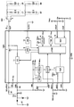
- FIG. 1 is a diagram showing a configuration example of a lamp system.
- the lamp system of this configuration example includes a lamp control device 100A and external parts externally attached to the lamp control device 100A.
- the external parts include a switch SW1, a left front lamp module LF, a left rear lamp module LR, a right front lamp module RF, and a right rear lamp module RR.
- Each lamp module includes an LED [light emitting diode]. Note that FIG. 1 illustrates a configuration in which one lamp module includes one LED, but one lamp module may include a plurality of LEDs.
- the lamp control device 100A is a semiconductor integrated circuit device (so-called LED driver IC) that receives the voltage output from the battery E1 and outputs an output current to each lamp module, and establishes an electrical connection with the outside of the device. Is equipped with a plurality of external terminals.
- LED driver IC semiconductor integrated circuit device
- the negative electrode of the battery E1 is connected to the ground terminal.
- the positive electrode of the battery E1 is connected to the anode of the backflow prevention diode.
- the cathode of the backflow prevention diode is connected to the external terminal VIN.
- the input voltage V IN ( ⁇ output voltage of the battery E1) is applied to the external terminal VIN.
- the input voltage V IN is applied to the external terminal SOURCE and the external terminal SE via the resistor R1.
- the divided voltage of the input voltage V IN is applied to the external terminal VDR.
- the input voltage V IN is applied to the external terminal SSE via the resistor R2. Since the current flowing through the path connecting the external terminal SSE and the external terminal OUT is set to be smaller than the current flowing through the path connecting the external terminal SOURCE and the external terminal OUT, the resistance value of the resistor R2 is the resistance value of the resistor R1. It is preferably larger.
- Constant voltage V REG generated in the interior of the lamp control device 100A is outputted from the external terminal VREG.
- a CR circuit for setting the blinking cycle of the lamp is connected to the external terminal DISC and the external terminal CRT.
- Ground potential is applied to the external terminal GND.
- a voltage indicating the detection threshold for short circuit abnormality detection is input to the external terminal VSCP.
- a voltage indicating a detection threshold value for open abnormality detection is input to the external terminal VOP.
- the common contact c of the switch SW1 is connected to the external terminal OUT and the external terminal OUTS.
- the external terminal OUT is an output terminal that outputs the drive current I O of the lamp.
- the external terminal OUTS is a terminal for monitoring the voltage applied to the external terminal OUT.
- the contact a of the switch SW1 is connected to the left front lamp module LF and the left rear lamp module LR.
- the contact b of the switch SW1 is connected to the front right lamp module RF and the rear right lamp module RR.
- the switch SW1 in order to turn on the left front lamp module LF and the left rear lamp module LR, the switch SW1 must be operated in advance to connect the common contact c and the contact a of the switch SW1. Similarly, in order to turn on the right front lamp module RF and the right rear lamp module RR, the switch SW1 must be operated in advance to connect the common contact c and the contact b of the switch SW1. When the switch SW1 is not operated at all, the common contact c is not connected to either the contact a or the contact b as shown in FIG.
- the left front lamp module LF, the right front lamp module RF, the left rear lamp module LR, and the right rear lamp module RR are series connection bodies of a current limiting resistor and an LED, respectively.
- the lamp control device 100A includes a bandgap reference voltage generation unit 1, a constant voltage generation unit 2, a duty control unit 3, a clock generation unit 4, a logic unit 5, a drive unit 6, a PMOS [P-channel]. [metal-oxide-semiconductor] transistor 7, low voltage malfunction prevention unit 8, overheat protection unit 9, abnormality detection unit 10, constant current unit 11, and voltage monitoring unit 12 are integrated.
- the bandgap reference voltage generation unit 1 generates a reference voltage V BG using the input voltage V IN applied to the external terminal VIN and supplies the reference voltage V BG to each unit of the lamp control device 100A.
- the constant voltage generator 2 uses the reference voltage V BG to generate a constant voltage V REG and supplies the constant voltage V REG to each unit of the lamp control device 100A.
- the duty control unit 3 controls the on-duty of the PWM [pulse width modulation] signal according to the voltage V DR (divided voltage of the input voltage V IN ) applied to the external terminal VDR. Specifically, the duty control unit 3 supplies the result of comparison (binarization signal) between the voltage V DR and the triangular wave voltage of a constant cycle generated by the clock generation unit 4 to the logic unit 5 as a PWM signal.
- the clock generation unit 4 generates a clock signal and a triangular wave voltage with a constant cycle, supplies the clock signal with a constant cycle to the logic unit 5, and supplies the triangular wave voltage with a constant cycle to the duty control unit 3.
- the logic unit 5 controls switching of the PMOS transistor 7. Specifically, the logic section 5 supplies a control signal to the drive section 6, and the drive section 6 drives the supply PMOS transistor 7 according to the control signal from the logic section 5.
- the logic unit 5 When controlling the blinking of the lamp, the logic unit 5 follows the first control mode in which the PMOS transistor 7 is turned off during the period corresponding to the M period of the clock signal and the PWM signal during the period corresponding to the N period of the clock signal.
- the second control mode in which the PMOS transistor 7 is turned on and off is alternately repeated.
- the logic unit 5 stops the operation of the drive unit 6.
- the logic unit 5 PWM-drives the PMOS transistor 7 via the drive unit 6. By PWM-driving the PMOS transistor 7, it becomes easy to light the lamp with a desired brightness.
- the M and N are natural numbers of 2 or more.
- the M and the N may be the same or different from each other.
- the logic unit 5 keeps the PMOS transistor 7 off during the period in which the lamp is prohibited from being turned on, when performing control to prohibit the lamp from being turned on.
- the low voltage malfunction prevention unit 8 locks out the operation of all the circuits of the lamp control device 100A except the constant voltage generation unit 2 when the input voltage V IN becomes equal to or lower than a predetermined value.
- the overheat protection unit 9 executes the overheat protection operation when detecting the overheat.
- the abnormality detection unit 10 When the abnormality detection unit 10 detects a lamp open abnormality and a lamp short-circuit abnormality, the abnormality detection unit 10 notifies the logic unit 5 of the occurrence of the abnormality.
- the constant current unit 11 is arranged on the path connecting the external terminal SSE and the external terminal OUT, and outputs a constant current to the external terminal OUT.
- the logic unit 5 intermittently operates the constant current unit 11 in the first control mode and stops the operation of the constant current unit 11 in the second control mode.
- the logic unit 5 intermittently operates the constant current unit 11 based on a clock signal of a constant cycle output from the clock generation unit 4.
- the voltage monitoring unit 12 monitors the voltage applied to the external terminal OUT. Specifically, the voltage monitoring unit 12 determines whether the voltage applied to the external terminal OUT is smaller than a first predetermined value and is larger than a second predetermined value (>first predetermined value), and the determination result is a logic unit. Notify 5. When the voltage applied to the external terminal OUT is smaller than the first predetermined value, the logic unit 5 starts the alternating switching between the first control mode and the second control mode. After that, when the voltage applied to the external terminal OUT becomes larger than the second predetermined value, the logic unit 5 ends the alternate switching between the first control mode and the second control mode, and fixes the control mode to the first control mode. To do.
- the second predetermined value is set to a value larger than the first predetermined value, and hysteresis is provided at the start and end of the alternate switching between the first control mode and the second control mode.
- the predetermined value and the second predetermined value may be the same value.
- FIG. 2 is a diagram showing a configuration example of the constant current unit 11 and the voltage monitoring unit 12.
- the constant current section 11 in this configuration example is composed of a PMOS transistor 11A, an operational amplifier 11B, and a constant voltage source 11C.
- the voltage monitoring unit 12 in this configuration example includes a comparator 12A and a constant voltage source 12B.
- the source of the PMOS transistor 11A and the inverting input terminal of the operational amplifier 11B are connected to the external terminal SSE, and the drain of the PMOS transistor 11A is connected to the external terminal OUT.
- the input voltage V IN is applied to the positive side of the constant voltage source 11C, and the negative side of the constant voltage source 11C is connected to the non-inverting input terminal of the operational amplifier 11B.
- the output terminal of the operational amplifier 11B is connected to the gate of the PMOS transistor 11A.
- the inverting input terminal of the comparator 12A is connected to the external terminal OUTS.
- the positive side of the constant voltage source 12B is connected to the non-inverting input terminal of the comparator 12A.
- the negative electrode side of the constant voltage source 12B is connected to the ground potential.
- the output signal of the comparator 12A is supplied to the logic unit 5.
- the constant current setting value of the constant current unit 11 is a value obtained by dividing the constant voltage value of the constant voltage source 11C by the resistance value of the resistor R2.
- the voltage monitoring unit 12 determines whether the voltage applied to the external terminal OUT is smaller than the first predetermined value or larger than the second predetermined value (>the first predetermined value). If the voltage applied to the external terminal OUT is smaller than the first predetermined value, the voltage monitoring unit 12 sets the signal supplied to the logic unit 5 to the HIGH level. When the voltage applied to the external terminal OUT is higher than the second predetermined value while the voltage applied to the external terminal OUT is higher than the first predetermined value, the voltage monitoring unit 12 outputs the signal supplied to the logic unit 5 to HIGH. Switch from level to LOW level.
- the constant current unit 11 makes the current flowing through the path connecting the external terminal SSE and the external terminal OUT constant current. Therefore, by reducing the constant current setting value of the constant current unit 11, it is possible to suppress the power loss caused by the leak current while the leak current is flowing.
- the constant current unit 11 since the constant current unit 11 is intermittently operated, the power loss caused by the leak current can be further suppressed when the leak current flows.
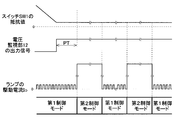
- FIG. 3 is a time chart of the lamp drive current I O. Note that FIG. 3 illustrates an example in which the PMOS transistor 7 is PWM-driven with an on-duty of 100% in the second control mode.
- the resistance value of the switch SW1 becomes sufficiently large.
- the voltage applied to the external terminal OUT does not become smaller than the first predetermined value.
- the logic unit 5 does not start the alternate switching between the first control mode and the second control mode unless the voltage applied to the external terminal OUT becomes smaller than the first predetermined value. In this case, the first control mode remains.
- the logic unit 5 does not start the alternate switching between the first control mode and the second control mode unless the voltage applied to the external terminal OUT becomes smaller than the first predetermined value. In this case also, the first control mode remains.
- the resistance value of the switch SW1 becomes sufficiently small.
- the voltage applied to the external terminal OUT becomes smaller than the first predetermined value, and alternate switching between the first control mode and the second control mode is started.
- the first control mode is switched to the second control mode only after the PT and HIGH levels are maintained for a certain period of time after the output signal of the voltage monitoring unit 12 becomes HIGH bell (see FIG. 3).
- the voltage monitored by the voltage monitoring unit 12 is the product of the constant current determined by the constant current unit 11 and the impedance of the load connected to the output terminal OUT.
- the impedance of the load connected to the output terminal OUT varies due to the variation in the forward voltage of the LED. Therefore, for example, by providing a resistor R3 connected in parallel to the lamp as in the modified example shown in FIG. 4, the voltage monitored by the voltage monitoring unit 12 is the constant current determined by the constant current unit 11, the switch SW1 and the switch SW1. It is the product of the combined resistance of the resistor R3. As a result, it is possible to accurately suppress erroneous lighting of the lamp due to the leak current.
- the logic unit 5 operates the constant current unit 11 intermittently in the first control mode.
- the power consumption can be reduced when the common contact c of the switch SW1 is not connected to either the contact a or the contact b. Further, this makes it possible to reduce the average current flowing through the lamp when the lamp is erroneously lit due to the leakage current, so that the brightness of the lamp at the time of erroneous lighting can be reduced.
- the constant current unit 11 may be continuously operated in the first control mode, though it is more disadvantageous than the present embodiment from the viewpoint of power consumption and the brightness of the lamp when erroneous lighting.
- the time chart of the lamp drive current I O is as shown in FIG. 5, for example.
- FIG. 6 is an external top view of the lamp control device 100A showing an arrangement example of external terminals of the lamp control device 100A.
- the same parts as those in FIG. 1 are designated by the same reference numerals.
- the external terminal SE, the external terminal SOURCE, the external terminal NC, the external terminal SSE, the external terminal NC, the external terminal VIN, the external terminal NC, the external terminal VDR, the external terminal VOP, And the external terminals PSSW are arranged side by side in this order.
- the external terminal OUT, the external terminal OUTS, the external terminal NC, the external terminal VREG, the external terminal NC, and the external terminal DISC are arranged along the second side S2 of the rectangular package P1 that is the side opposite to the first side S1.
- the external terminal CRT, the external terminal VSCP, the external terminal NC, and the external terminal GND are arranged side by side in this order.
- the external terminal OUT and the external terminal OUTS are preferably provided on the same side of the rectangular package. Furthermore, it is desirable that no other external terminal exists between the external terminal OUT and the external terminal OUTS. This facilitates the connection between the switch SW1 and the external terminals OUT and OUTS.
- Each external terminal NC is a terminal that is not connected to the internal circuit of the rectangular package P1. Although illustration of the external terminal PSSW is omitted in FIG. 1 and the like, consumption of the external terminal PSSW in the standby mode is achieved by connecting the lower side (low potential side) of the resistive voltage division to the external terminal PSSW instead of the ground of the resistive voltage division. This is a terminal that reduces the current.
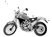
- FIG. 7 is an external view of a motorcycle.
- the motorcycle A includes a flasher lamp A1 provided on the front left side of the motorcycle, a flasher lamp A2 provided on the rear left side of the motorcycle, and a flasher lamp (not shown in FIG. 7) provided on the front right side of the motorcycle.
- the motorcycle includes a flasher lamp A3 provided on the right rear side of the motorcycle and a battery A4 serving as a power source for the flasher lamp A3.
- the lamp control device 100A described above can be suitably used as a device that controls the lighting of each flasher lamp of the motorcycle A.
- the switch SW1 shown in FIG. 1 becomes a flasher switch and is operated by the driver of the motorcycle A.
- the lamp control device 100A may be used to configure the lamp system shown in FIG.
- the external terminal OUTS is connected to the ground potential.
- the output signal of the voltage monitoring unit 12 becomes HIGH level regardless of the voltage applied to the external terminal OUT. That is, the voltage monitoring unit 12 is disabled and does not monitor the voltage applied to the external terminal OUT.
- the abnormality detection unit 10 determines that the current flowing through the resistor R1 is a threshold value. In the following cases, it has a function of detecting that the common contact c of the switch SW1 is not connected to either the contact a or the contact b.
- the logic unit 5 When the abnormality detecting unit 10 detects that the common contact c of the switch SW1 is not connected to either the contact a or the contact b, the logic unit 5 operates in the second control mode. Even if there is, the second control mode is switched to the first control mode at the switching timing based on the clock signal. Therefore, when the common contact c of the switch SW1 is not connected to either the contact a or the contact b, the second control mode has at most one cycle of the clock signal.
- the abnormality detection unit 10 does not detect that the common contact c of the switch SW1 is not connected to either the contact a or the contact b. Thereby, the logic unit 5 alternately switches between the first control mode and the second control mode.
- FIG. 9 is a diagram showing another configuration example of the lamp system.
- the lamp system of this configuration example includes a lamp control device 100B and external parts externally attached thereto.
- the external parts include a resistor R3, a switch SW1, a left front lamp module LF, a left rear lamp module LR, a right front lamp module RF, and a right rear lamp module RR.
- Each lamp module comprises an LED.
- FIG. 9 illustrates a configuration in which one lamp module includes one LED, one lamp module may include a plurality of LEDs.
- Specific configuration examples of the left front lamp module LF, the left rear lamp module LR, the right front lamp module RF, and the right rear lamp module RR in the present embodiment are the left front lamp module LF and the left front lamp module LF in the first embodiment. This is different from the specific configuration example of the rear lamp module LR, the right front lamp module RF, and the right rear lamp module RR.
- the lamp control device 100B is a semiconductor integrated circuit device (so-called LED driver IC) that receives the voltage output from the battery E1 and outputs an output current to each lamp module, and establishes an electrical connection with the outside of the device. Is equipped with a plurality of external terminals.
- LED driver IC semiconductor integrated circuit device
- the lamp control device 100B does not include the external terminal SSE.
- the external terminal OUT is an output terminal that outputs a lamp drive current.
- the input voltage V IN is applied to the other end of the resistor R3.
- the contact a of the switch SW1 is connected to the left front lamp module LF and the left rear lamp module LR.
- the contact b of the switch SW1 is connected to the front right lamp module RF and the rear right lamp module RR.
- the switch SW1 in order to turn on the left front lamp module LF and the left rear lamp module LR, the switch SW1 must be operated in advance to connect the common contact c and the contact a of the switch SW1. Similarly, in order to turn on the right front lamp module RF and the right rear lamp module RR, the switch SW1 must be operated in advance to connect the common contact c and the contact b of the switch SW1. When the switch SW1 is not operated at all, as shown in FIG. 9, the common contact c is not connected to either the contact a or the contact b.
- Each of the left front lamp module LF and the right front lamp module RF includes a current limiting resistor and a resistor R4_1 connected in parallel to the series connection body of the LEDs.
- the left rear lamp module LR and the right rear lamp module RR each include a current limiting resistor and a resistor R4_2 connected in parallel to the series connection body of the LEDs.
- the lamp control device 100B includes a bandgap reference voltage generation unit 1, a constant voltage generation unit 2, a duty control unit 3, a clock generation unit 4, a logic unit 5, a driving unit 6, a PMOS transistor 7, The low voltage malfunction prevention unit 8, the overheat protection unit 9, the abnormality detection unit 10, and the state detection unit 200 are integrated.
- the bandgap reference voltage generation unit 1 generates a reference voltage V BG using the input voltage V IN applied to the external terminal VIN and supplies the reference voltage V BG to each unit of the lamp control device 100B.
- the constant voltage generator 2 uses the reference voltage V BG to generate a constant voltage V REG and supplies the constant voltage V REG to each unit of the lamp control device 100B.
- the logic unit 5 When controlling the blinking of the lamp, the logic unit 5 has a first control mode (light-off control) in which the MOS transistor 7 is turned off during a period corresponding to M cycles of the clock signal, and a period corresponding to N cycles of the clock signal.
- the second control mode (lighting control) for switching between the ON state and the OFF state of the MOS transistor 7 according to the middle PWM signal is alternately repeated.
- the M and N are natural numbers of 2 or more.
- the M and the N may be the same or different from each other.
- the state detection unit 200 detects the state of the switch SW1. Specifically, the state detection unit 200 determines whether the resistance value of the switch SW1 is smaller than a predetermined value, and notifies the logic unit 5 of the determination result.
- FIG. 10 is a diagram showing a first configuration example of the state detection unit 200.
- the state detection unit 200 in this configuration example includes a resistor R11, a resistor R12, and a comparator CMP1.
- the input voltage V IN is applied to one end of the resistor R11.
- the other end of the resistor R11 and one end of the resistor R12 are connected to the non-inverting input terminal of the comparator CMP1.
- the ground potential is applied to the other end of the resistor R12.
- the external terminal OUT is connected to the inverting input terminal of the comparator CMP1.
- the divided voltage of the input voltage V IN is applied to the inverting input terminal of the comparator CMP1.
- the ratio of the resistance value of the resistor R11 to the resistance value of the resistor R12 is set to 9. Therefore, as shown in FIG. 10, 0.1V IN is applied to the non-inverting input terminal of the comparator CMP1. That is, the following expression (1) is established.
- V + is a voltage applied to the non-inverting input terminal of the comparator CMP1.
- V + 0.1 ⁇ V IN (1)
- V ⁇ is the voltage applied to the inverting input terminal of the comparator CMP1
- R 3 is the resistance value of the resistor R3
- R 4 is the resistor R4_1 and the left rear lamp of the front left lamp module LF (see FIG. 9).
- R SW are the resistance values of the switch SW1.
- V ⁇ V IN ⁇ (R SW +R 4 )/(R SW +R 3 +R 4 ).
- the resistance value R SW of the switch SW1 increases to some extent. Therefore, the resistance value R 3 and the combined resistance value R 4 are set so that the above equation (4) does not hold when a leak current flows through the switch SW1. In other words, the detection sensitivity of the leak current can be adjusted by setting the resistance value R 3 and the combined resistance value R 4 .
- the error factor for detecting the leak current is “9” in the above equation (4). That is, the error with respect to the detection of the leak current is about the error of the voltage division ratio of the voltage dividing circuit configured by the resistors R11 and R12. Therefore, the state detection unit 200 in the present configuration example can detect the leak current of the switch SW1 with higher accuracy than the lamp control device proposed in Patent Document 1.
- the constant voltage V REG may be used instead of the input voltage V IN .
- FIG. 11 is a diagram showing a second configuration example of the state detection unit 200.
- the state detection unit 200 in this configuration example differs from the state detection unit 200 in the first configuration example in that it includes a constant current source CS1 instead of the resistor R11, and further includes a constant current source CS2 and an adjustment circuit ADJ1. The point is the same as the state detection unit 200 in the first configuration example.
- the resistor R3 is not connected to the external terminal OUT as shown in FIG.
- the power supply voltage of the constant current sources CS1 and CS2 is the input voltage V IN .
- the constant voltage V REG may be used as the power supply voltage for the constant current sources CS1 and CS2 instead of the input voltage V IN .
- the constant current source CS2 supplies a constant current to the external terminal OUT.
- the adjusting circuit ADJ1 adjusts the ratio of the value of the constant current output from the constant current source CS2 to the value of the constant current output from the constant current source CS1 according to the value of the resistor connected to the external terminal ADJ. It can be adjusted detection sensitivity of the leakage current by the ratio and set the combined resistance value R 4 value of the constant current output from the constant current source CS2 to the value of the constant current output from the constant current source CS1.
- the error for the detection of the leak current is about the error of the ratio of the constant current value output from the constant current source CS2 to the constant current value output from the constant current source CS1. Therefore, the state detection unit 200 in the present configuration example can detect the leak current of the switch SW1 with higher accuracy than the lamp control device proposed in Patent Document 1.
- the above-described lamp control device 100B can be suitably used as a device for performing lighting control of each flasher lamp of the motorcycle A shown in FIG. 7 described above.
- the switch SW1 shown in FIG. 9 becomes a flasher switch and is operated by the driver of the motorcycle A.
- the logic of the output signal SG1 may be reversed from that of the second embodiment.
- the resistor R3 may be built in the lamp control device 100B. However, from the viewpoint of increasing the degree of freedom in adjusting the detection sensitivity of the leakage current, it is desirable that the resistor R3 be an external component as in the second embodiment.
Landscapes
- Engineering & Computer Science (AREA)
- Mechanical Engineering (AREA)
- Lighting Device Outwards From Vehicle And Optical Signal (AREA)
- Circuit Arrangement For Electric Light Sources In General (AREA)
Abstract
Description
<1-1.ランプシステムの構成>
図1はランプシステムの一構成例を示す図である。本構成例のランプシステムは、ランプ制御装置100Aと、これに外付けされる外付け部品と、を備える。外付け部品は、スイッチSW1、左前用ランプモジュールLF、左後用ランプモジュールLR、右前用ランプモジュールRF、及び右後用ランプモジュールRRを含む。各ランプモジュールはLED[light emitting diode]を備える。なお、図1では、1つのランプモジュールが1つのLEDを備える構成を図示しているが、1つのランプモジュールが複数のLEDを備える構成であってもよい。
引き続き、図1を参照しながら、ランプ制御装置100Aの内部構成について説明する。ランプ制御装置100Aは、バンドギャップ型基準電圧生成部1と、定電圧生成部2と、デューティ制御部3と、クロック生成部4と、ロジック部5と、駆動部6と、PMOS[P-channel metal-oxide-semiconductor]トランジスタ7と、低電圧誤動作防止部8と、過熱保護部9と、異常検出部10と、定電流部11と、電圧監視部12と、を集積化している。
図2は、定電流部11及び電圧監視部12の一構成例を示す図である。なお、図2において図1と同一の部分には同一の符号を付す。本構成例における定電流部11は、PMOSトランジスタ11A、オペアンプ11B、及び定電圧源11Cによって構成される。本構成例における電圧監視部12は、コンパレータ12A及び定電圧源12Bによって構成される。
次に、図1に示すランプシステムの動作について図3を参照して説明する。図3は、ランプの駆動電流IOのタイムチャートである。なお、図3は、第2制御モードにおいてPMOSトランジスタ7がオンデューティ100%でPWM駆動される例を示している。
図6は、ランプ制御装置100Aの外部端子の配置例を示すランプ制御装置100Aの外観上面図である。なお、図6において図1と同一の部分には同一の符号を付す。
図7は、自動二輪車の外観図である。本図の自動二輪車Aは、いわゆる中型二輪(=日本の道路交通法において、排気量50cc超400cc以下の車両区分に属する普通自動二輪車に相当)と呼ばれる車両の一種である。自動二輪車Aは、自動二輪車の左側前方に設けられるフラッシャーランプA1と、自動二輪車の左側後方に設けられるフラッシャーランプA2と、自動二輪車の右側前方に設けられるフラッシャーランプ(図7において不図示)と、自動二輪車の右側後方に設けられるフラッシャーランプA3と、それらの電源となるバッテリA4と、を備える。
上記の第1実施形態では、ランプとしてLEDを用いた構成を例に挙げたが、例えば、ランプとしてハロゲンランプ、キセノンランプ、有機EL[electro-luminescence]素子等を用いることも可能である。
<2-1.ランプシステムの構成>
図9はランプシステムの他の構成例を示す図である。なお、図9において、図1と同一の部分には同一の符号を付し、詳細な説明を適宜省略する。本構成例のランプシステムは、ランプ制御装置100Bと、これに外付けされる外付け部品と、を備える。外付け部品は、抵抗R3、スイッチSW1、左前用ランプモジュールLF、左後用ランプモジュールLR、右前用ランプモジュールRF、及び右後用ランプモジュールRRを含む。各ランプモジュールはLEDを備える。なお、図9では、1つのランプモジュールが1つのLEDを備える構成を図示しているが、1つのランプモジュールが複数のLEDを備える構成であってもよい。本実施形態における左前用ランプモジュールLF、左後用ランプモジュールLR、右前用ランプモジュールRF、及び右後用ランプモジュールRRの具体的な構成例は、第1実施形態における左前用ランプモジュールLF、左後用ランプモジュールLR、右前用ランプモジュールRF、及び右後用ランプモジュールRRの具体的な構成例とは異なる。
引き続き、図9を参照しながら、ランプ制御装置100Bの内部構成について説明する。ランプ制御装置100Bは、バンドギャップ型基準電圧生成部1と、定電圧生成部2と、デューティ制御部3と、クロック生成部4と、ロジック部5と、駆動部6と、PMOSトランジスタ7と、低電圧誤動作防止部8と、過熱保護部9と、異常検出部10と、状態検出部200と、を集積化している。
(第1構成例)
図10は、状態検出部200の第1構成例を示す図である。なお、図10において図9と同一の部分には同一の符号を付す。本構成例における状態検出部200は、抵抗R11、抵抗R12、及びコンパレータCMP1によって構成される。
V+=0.1×VIN …(1)
V-=VIN×(RSW+R4)/(RSW+R3+R4) …(2)
V-<V+ …(3)
VIN×(RSW+R4)/(RSW+R3+R4)<0.1×VIN
RSW<(R3/9)-R4 …(4)
図11は、状態検出部200の第2構成例を示す図である。なお、図11において図10と同一の部分には同一の符号を付す。本構成例における状態検出部200は、抵抗R11の代わりに定電流源CS1を備え、さらに定電流源CS2及び調整回路ADJ1を備える点で第1構成例における状態検出部200と異なり、それ以外の点で第1構成例における状態検出部200と同一である。
上述したランプ制御装置100Bは、上述したランプ制御装置100Aと同様に、上述した図7に示す自動二輪車Aの各フラッシャーランプの点灯制御を行う装置として好適に用いることができる。上述したランプ制御装置100Bを自動二輪車Aの各フラッシャーランプの点灯制御を行う装置として用いた場合、図9に示すスイッチSW1はフラッシャースイッチとなり、自動二輪車Aの運転者によって操作される。
上記の第2実施形態では、ランプとしてLEDを用いた構成を例に挙げたが、例えば、ランプとしてハロゲンランプ、キセノンランプ、有機EL素子等を用いることも可能である。
11 定電流部
12 電圧監視部
200 状態検出部
CMP1 コンパレータ
OUT 出力端子(外部端子)
R1、R2、RSW 抵抗
A 自動二輪車(車両)
Claims (11)
- 第1入力端子と、
第2入力端子と、
外部スイッチを介してランプに接続可能に構成され、前記ランプの駆動電流を出力する出力端子と、
前記第1入力端子と前記出力端子とを繋ぐ第1経路上に設けられる内部スイッチと、
前記第2入力端子と前記出力端子とを繋ぐ第2経路上に設けられる定電流部と、
前記出力端子に印加される電圧を監視する電圧監視部と、
前記電圧監視部の監視結果に基づき前記内部スイッチを制御する制御部と、
を備える、ランプ制御装置。 - 前記制御部は、
前記出力端子に印加される電圧が第1所定値より小さい場合、第1制御モードと第2制御モードとの交互切り替えを開始する、請求項1に記載のランプ制御装置。 - 前記制御部は、
前記第1制御モードと前記第2制御モードとの交互切り替えを開始した後、前記出力端子に印加される電圧が第2所定値より大きくなると、前記第1制御モードと前記第2制御モードとの交互切り替えを終了し、制御モードを前記第1制御モードに固定する、請求項2に記載のランプ制御装置。 - 前記第2所定値は前記第1所定値より大きい、請求項3に記載のランプ制御装置。
- 前記制御部は、前記第2制御モード時に前記内部スイッチをPWM駆動する、請求項2~4のいずれか一項に記載のランプ制御装置。
- 前記制御部は、前記第1制御モード時に前記定電流部を間欠動作させる、請求項2~5のいずれか一項に記載のランプ制御装置。
- 前記制御部は、前記第2制御モード時に前記定電流部の動作を停止させる、請求項2~6のいずれか一項に記載のランプ制御装置。
- 請求項1~7のいずれか一項に記載のランプ制御装置と、
前記外部スイッチと、
前記ランプと、
を備える、ランプシステム。 - 第1抵抗及び第2抵抗を備え、
前記第1抵抗の一端及び前記第2抵抗の一端に入力電圧が印加され、
前記第1抵抗の他端が前記第1入力端子に接続され、
前記第2抵抗の他端が前記第2入力端子に接続され、
前記第2抵抗の抵抗値は前記第1抵抗の抵抗値より大きい、請求項8に記載のランプシステム。 - 請求項8又は請求項9に記載のランプシステムと、
前記ランプシステムの電源となるバッテリと、
を備える、車両。 - 前記車両は自動二輪車であり、
前記スイッチは、フラッシャースイッチであり、
前記ランプは、フラッシャーランプである、請求項10に記載の車両。
Priority Applications (5)
| Application Number | Priority Date | Filing Date | Title |
|---|---|---|---|
| JP2020559171A JP7291725B2 (ja) | 2018-12-14 | 2019-12-02 | ランプ制御装置 |
| CN201980082138.1A CN113226904B (zh) | 2018-12-14 | 2019-12-02 | 灯控制装置 |
| US17/298,807 US11919441B2 (en) | 2018-12-14 | 2019-12-02 | Lamp control device |
| DE112019006217.4T DE112019006217T5 (de) | 2018-12-14 | 2019-12-02 | Lampensteuervorrichtung |
| US18/426,602 US12257948B2 (en) | 2018-12-14 | 2024-01-30 | Lamp control device |
Applications Claiming Priority (4)
| Application Number | Priority Date | Filing Date | Title |
|---|---|---|---|
| JP2018234402 | 2018-12-14 | ||
| JP2018-234402 | 2018-12-14 | ||
| JP2019-061305 | 2019-03-27 | ||
| JP2019061305 | 2019-03-27 |
Related Child Applications (2)
| Application Number | Title | Priority Date | Filing Date |
|---|---|---|---|
| US17/298,807 A-371-Of-International US11919441B2 (en) | 2018-12-14 | 2019-12-02 | Lamp control device |
| US18/426,602 Continuation US12257948B2 (en) | 2018-12-14 | 2024-01-30 | Lamp control device |
Publications (1)
| Publication Number | Publication Date |
|---|---|
| WO2020121864A1 true WO2020121864A1 (ja) | 2020-06-18 |
Family
ID=71075688
Family Applications (1)
| Application Number | Title | Priority Date | Filing Date |
|---|---|---|---|
| PCT/JP2019/046996 Ceased WO2020121864A1 (ja) | 2018-12-14 | 2019-12-02 | ランプ制御装置 |
Country Status (5)
| Country | Link |
|---|---|
| US (2) | US11919441B2 (ja) |
| JP (2) | JP7291725B2 (ja) |
| CN (1) | CN113226904B (ja) |
| DE (1) | DE112019006217T5 (ja) |
| WO (1) | WO2020121864A1 (ja) |
Families Citing this family (2)
| Publication number | Priority date | Publication date | Assignee | Title |
|---|---|---|---|---|
| JP7291725B2 (ja) | 2018-12-14 | 2023-06-15 | ローム株式会社 | ランプ制御装置 |
| CN112248934B (zh) * | 2020-09-29 | 2025-01-24 | 蔚来汽车科技(安徽)有限公司 | 车辆灯光提示控制装置的状态检测方法、装置及车辆 |
Citations (2)
| Publication number | Priority date | Publication date | Assignee | Title |
|---|---|---|---|---|
| WO2013065106A1 (ja) * | 2011-10-31 | 2013-05-10 | 新電元工業株式会社 | 方向指示灯制御装置、方向指示装置および方向指示装置の制御方法 |
| JP2014040142A (ja) * | 2012-08-21 | 2014-03-06 | Rohm Co Ltd | リーク電流検出回路、半導体装置、led照明装置、車両 |
Family Cites Families (17)
| Publication number | Priority date | Publication date | Assignee | Title |
|---|---|---|---|---|
| DE3118240C2 (de) * | 1981-05-08 | 1984-08-02 | Telefunken electronic GmbH, 7100 Heilbronn | Blinkgeber |
| US4972174A (en) * | 1989-07-21 | 1990-11-20 | Onan Lance C | Motorcycle turn signal control circuit |
| US5808545A (en) * | 1994-05-20 | 1998-09-15 | Brueggemann; Douglas C. | Integrated vehicular electronic signalling system |
| US7646291B2 (en) * | 2004-11-15 | 2010-01-12 | Safecode, Inc. | Method for automotive lamp control |
| EP1821386A2 (en) | 2006-02-17 | 2007-08-22 | Power Systems Co., Ltd. | Charging apparatus for capacitor storage type power source and discharging apparatus for capacitor storage type power source |
| JP3907123B1 (ja) | 2006-02-17 | 2007-04-18 | 株式会社パワーシステム | キャパシタ蓄電電源用充電装置 |
| WO2011055533A1 (ja) * | 2009-11-04 | 2011-05-12 | ローム株式会社 | バックライト用ledストリングの駆動回路および駆動方法、ならびにそれを用いたバックライトおよびディスプレイ装置 |
| JP5425004B2 (ja) * | 2010-07-05 | 2014-02-26 | 本田技研工業株式会社 | 鞍乗型車両の発光ダイオード点灯回路 |
| US9945910B2 (en) | 2011-03-31 | 2018-04-17 | Renesas Electronics Corporation | Voltage monitoring module and voltage monitoring system which compares voltages to determine leakage |
| JP2013071593A (ja) * | 2011-09-28 | 2013-04-22 | Yamaha Motor Co Ltd | 車両用フラッシャースイッチ |
| TWI449467B (zh) | 2012-03-12 | 2014-08-11 | Anteya Technology Corp | High-power power switch switching dimmer, power switch switching dimming system, dimming device and transmission power and dimming instructions |
| EP3127795B1 (en) | 2014-03-31 | 2019-03-13 | Honda Motor Co., Ltd. | Vehicle led lighting device system |
| KR102360117B1 (ko) * | 2014-12-30 | 2022-02-07 | 주식회사 엘엑스세미콘 | 리어 콤비네이션 램프 장치 및 그 감시 방법 |
| JP6566511B2 (ja) * | 2015-04-07 | 2019-08-28 | 株式会社小糸製作所 | 点灯回路 |
| JP6400045B2 (ja) | 2016-06-01 | 2018-10-03 | 株式会社ミツバ | 灯体制御装置及び灯体点灯システム |
| CN108601162B (zh) * | 2018-07-03 | 2021-07-06 | 上海路傲电子科技有限公司 | Led照明线性恒流驱动电路 |
| JP7291725B2 (ja) | 2018-12-14 | 2023-06-15 | ローム株式会社 | ランプ制御装置 |
-
2019
- 2019-12-02 JP JP2020559171A patent/JP7291725B2/ja active Active
- 2019-12-02 WO PCT/JP2019/046996 patent/WO2020121864A1/ja not_active Ceased
- 2019-12-02 US US17/298,807 patent/US11919441B2/en active Active
- 2019-12-02 DE DE112019006217.4T patent/DE112019006217T5/de active Pending
- 2019-12-02 CN CN201980082138.1A patent/CN113226904B/zh active Active
-
2023
- 2023-06-05 JP JP2023092122A patent/JP7503177B2/ja active Active
-
2024
- 2024-01-30 US US18/426,602 patent/US12257948B2/en active Active
Patent Citations (2)
| Publication number | Priority date | Publication date | Assignee | Title |
|---|---|---|---|---|
| WO2013065106A1 (ja) * | 2011-10-31 | 2013-05-10 | 新電元工業株式会社 | 方向指示灯制御装置、方向指示装置および方向指示装置の制御方法 |
| JP2014040142A (ja) * | 2012-08-21 | 2014-03-06 | Rohm Co Ltd | リーク電流検出回路、半導体装置、led照明装置、車両 |
Also Published As
| Publication number | Publication date |
|---|---|
| CN113226904B (zh) | 2022-12-02 |
| JP7291725B2 (ja) | 2023-06-15 |
| DE112019006217T5 (de) | 2021-09-02 |
| US20220055538A1 (en) | 2022-02-24 |
| JP7503177B2 (ja) | 2024-06-19 |
| US20240166131A1 (en) | 2024-05-23 |
| JPWO2020121864A1 (ja) | 2021-11-04 |
| US12257948B2 (en) | 2025-03-25 |
| CN113226904A (zh) | 2021-08-06 |
| US11919441B2 (en) | 2024-03-05 |
| JP2023101804A (ja) | 2023-07-21 |
Similar Documents
| Publication | Publication Date | Title |
|---|---|---|
| JP5989455B2 (ja) | リーク電流検出回路、半導体装置、led照明装置、車両 | |
| US10360969B2 (en) | Light emitting element driving semiconductor integrated circuit, light emitting element driving device, light emitting device, and vehicle | |
| US10383193B2 (en) | Lighting circuit and vehicle lamp employing same | |
| US8330375B2 (en) | Vehicle lamp lighting control device | |
| JP6757579B2 (ja) | 発光素子駆動装置、発光装置、車両 | |
| EP3244700B1 (en) | Ground fault detection circuit, abnormality detection circuit, light emitting device, vehicle | |
| JP2006210219A (ja) | 車両用灯具の点灯制御回路 | |
| JP2006073400A (ja) | 車両用灯具の点灯制御回路 | |
| JP6821835B2 (ja) | 点灯回路およびそれを用いた車両用灯具 | |
| KR20170045218A (ko) | Led 주행등 제어 및 상태를 위한 장치 및 방법 | |
| JP7503177B2 (ja) | ランプ制御装置 | |
| EP2410820B1 (en) | Semiconductor light source lighting circuit and control method | |
| EP2200406B1 (en) | Controller for vehicular lamp | |
| JP6173874B2 (ja) | 車両用灯具 | |
| US7327203B2 (en) | PWM signal generation circuit and PWM control circuit | |
| JP2014136532A (ja) | 半導体装置 | |
| JP4780775B2 (ja) | 電源装置のledランプ用保護回路 | |
| WO2012111041A1 (ja) | Led点灯装置 | |
| KR101903970B1 (ko) | 차량 led 램프의 텔-테일 회로 | |
| JP7675637B2 (ja) | 点灯回路、及び車両用灯具 | |
| JP6249555B2 (ja) | 車両用灯具 | |
| WO2024079980A1 (ja) | 半導体装置、発光装置、車両 | |
| JP2024047822A (ja) | 点灯回路 | |
| JPH1151984A (ja) | 異常電流検知回路 | |
| ITMI20081709A1 (it) | Circuito di pilotaggio di una serie di diodi ad emissione di luce |
Legal Events
| Date | Code | Title | Description |
|---|---|---|---|
| 121 | Ep: the epo has been informed by wipo that ep was designated in this application |
Ref document number: 19897204 Country of ref document: EP Kind code of ref document: A1 |
|
| ENP | Entry into the national phase |
Ref document number: 2020559171 Country of ref document: JP Kind code of ref document: A |
|
| 122 | Ep: pct application non-entry in european phase |
Ref document number: 19897204 Country of ref document: EP Kind code of ref document: A1 |
|
| WWG | Wipo information: grant in national office |
Ref document number: 202117025271 Country of ref document: IN |