WO2024079980A1 - 半導体装置、発光装置、車両 - Google Patents
半導体装置、発光装置、車両 Download PDFInfo
- Publication number
- WO2024079980A1 WO2024079980A1 PCT/JP2023/029700 JP2023029700W WO2024079980A1 WO 2024079980 A1 WO2024079980 A1 WO 2024079980A1 JP 2023029700 W JP2023029700 W JP 2023029700W WO 2024079980 A1 WO2024079980 A1 WO 2024079980A1
- Authority
- WO
- WIPO (PCT)
- Prior art keywords
- light
- switch element
- current source
- semiconductor device
- emitting element
- Prior art date
Links
- 239000004065 semiconductor Substances 0.000 title claims abstract description 74
- 238000001514 detection method Methods 0.000 claims abstract description 142
- 238000003745 diagnosis Methods 0.000 claims abstract description 96
- 238000012544 monitoring process Methods 0.000 claims abstract description 20
- 230000004044 response Effects 0.000 claims description 5
- 230000007704 transition Effects 0.000 claims description 4
- 238000010586 diagram Methods 0.000 description 53
- 238000004458 analytical method Methods 0.000 description 3
- 230000000694 effects Effects 0.000 description 2
- 239000011159 matrix material Substances 0.000 description 2
- 238000000034 method Methods 0.000 description 2
- 230000004048 modification Effects 0.000 description 2
- 238000012986 modification Methods 0.000 description 2
- 230000004397 blinking Effects 0.000 description 1
- 238000006243 chemical reaction Methods 0.000 description 1
- 238000005401 electroluminescence Methods 0.000 description 1
- 230000005669 field effect Effects 0.000 description 1
- 230000006872 improvement Effects 0.000 description 1
- 229910044991 metal oxide Inorganic materials 0.000 description 1
- 150000004706 metal oxides Chemical class 0.000 description 1
- 230000008520 organization Effects 0.000 description 1
Images


Classifications
-
- B—PERFORMING OPERATIONS; TRANSPORTING
- B60—VEHICLES IN GENERAL
- B60Q—ARRANGEMENT OF SIGNALLING OR LIGHTING DEVICES, THE MOUNTING OR SUPPORTING THEREOF OR CIRCUITS THEREFOR, FOR VEHICLES IN GENERAL
- B60Q11/00—Arrangement of monitoring devices for devices provided for in groups B60Q1/00 - B60Q9/00
-
- H—ELECTRICITY
- H05—ELECTRIC TECHNIQUES NOT OTHERWISE PROVIDED FOR
- H05B—ELECTRIC HEATING; ELECTRIC LIGHT SOURCES NOT OTHERWISE PROVIDED FOR; CIRCUIT ARRANGEMENTS FOR ELECTRIC LIGHT SOURCES, IN GENERAL
- H05B45/00—Circuit arrangements for operating light-emitting diodes [LED]
- H05B45/10—Controlling the intensity of the light
- H05B45/14—Controlling the intensity of the light using electrical feedback from LEDs or from LED modules
-
- H—ELECTRICITY
- H05—ELECTRIC TECHNIQUES NOT OTHERWISE PROVIDED FOR
- H05B—ELECTRIC HEATING; ELECTRIC LIGHT SOURCES NOT OTHERWISE PROVIDED FOR; CIRCUIT ARRANGEMENTS FOR ELECTRIC LIGHT SOURCES, IN GENERAL
- H05B45/00—Circuit arrangements for operating light-emitting diodes [LED]
- H05B45/30—Driver circuits
- H05B45/32—Pulse-control circuits
- H05B45/325—Pulse-width modulation [PWM]
-
- H—ELECTRICITY
- H05—ELECTRIC TECHNIQUES NOT OTHERWISE PROVIDED FOR
- H05B—ELECTRIC HEATING; ELECTRIC LIGHT SOURCES NOT OTHERWISE PROVIDED FOR; CIRCUIT ARRANGEMENTS FOR ELECTRIC LIGHT SOURCES, IN GENERAL
- H05B45/00—Circuit arrangements for operating light-emitting diodes [LED]
- H05B45/40—Details of LED load circuits
- H05B45/44—Details of LED load circuits with an active control inside an LED matrix
-
- H—ELECTRICITY
- H05—ELECTRIC TECHNIQUES NOT OTHERWISE PROVIDED FOR
- H05B—ELECTRIC HEATING; ELECTRIC LIGHT SOURCES NOT OTHERWISE PROVIDED FOR; CIRCUIT ARRANGEMENTS FOR ELECTRIC LIGHT SOURCES, IN GENERAL
- H05B45/00—Circuit arrangements for operating light-emitting diodes [LED]
- H05B45/50—Circuit arrangements for operating light-emitting diodes [LED] responsive to malfunctions or undesirable behaviour of LEDs; responsive to LED life; Protective circuits
- H05B45/54—Circuit arrangements for operating light-emitting diodes [LED] responsive to malfunctions or undesirable behaviour of LEDs; responsive to LED life; Protective circuits in a series array of LEDs
-
- H—ELECTRICITY
- H05—ELECTRIC TECHNIQUES NOT OTHERWISE PROVIDED FOR
- H05B—ELECTRIC HEATING; ELECTRIC LIGHT SOURCES NOT OTHERWISE PROVIDED FOR; CIRCUIT ARRANGEMENTS FOR ELECTRIC LIGHT SOURCES, IN GENERAL
- H05B47/00—Circuit arrangements for operating light sources in general, i.e. where the type of light source is not relevant
- H05B47/10—Controlling the light source
- H05B47/105—Controlling the light source in response to determined parameters
-
- H—ELECTRICITY
- H05—ELECTRIC TECHNIQUES NOT OTHERWISE PROVIDED FOR
- H05B—ELECTRIC HEATING; ELECTRIC LIGHT SOURCES NOT OTHERWISE PROVIDED FOR; CIRCUIT ARRANGEMENTS FOR ELECTRIC LIGHT SOURCES, IN GENERAL
- H05B47/00—Circuit arrangements for operating light sources in general, i.e. where the type of light source is not relevant
- H05B47/10—Controlling the light source
- H05B47/16—Controlling the light source by timing means
-
- H—ELECTRICITY
- H05—ELECTRIC TECHNIQUES NOT OTHERWISE PROVIDED FOR
- H05B—ELECTRIC HEATING; ELECTRIC LIGHT SOURCES NOT OTHERWISE PROVIDED FOR; CIRCUIT ARRANGEMENTS FOR ELECTRIC LIGHT SOURCES, IN GENERAL
- H05B47/00—Circuit arrangements for operating light sources in general, i.e. where the type of light source is not relevant
- H05B47/20—Responsive to malfunctions or to light source life; for protection
- H05B47/23—Responsive to malfunctions or to light source life; for protection of two or more light sources connected in series
-
- H—ELECTRICITY
- H05—ELECTRIC TECHNIQUES NOT OTHERWISE PROVIDED FOR
- H05B—ELECTRIC HEATING; ELECTRIC LIGHT SOURCES NOT OTHERWISE PROVIDED FOR; CIRCUIT ARRANGEMENTS FOR ELECTRIC LIGHT SOURCES, IN GENERAL
- H05B47/00—Circuit arrangements for operating light sources in general, i.e. where the type of light source is not relevant
- H05B47/20—Responsive to malfunctions or to light source life; for protection
- H05B47/25—Circuit arrangements for protecting against overcurrent
Definitions
- This disclosure relates to a semiconductor device, and a light-emitting device and vehicle using the same.
- Semiconductor devices e.g., matrix switch ICs [integrated circuits] or bypass switch ICs
- matrix switch ICs integrated circuits
- bypass switch ICs bypass switch ICs
- LEDs light emitting diodes
- Patent Document 1 As an example of related prior art, Patent Document 1 can be mentioned.
- the semiconductor device disclosed in this specification includes a switch element configured to be connected in parallel to a light-emitting element, a detection circuit configured to generate a detection signal by comparing the voltage across the switch element with a predetermined threshold voltage, and a fault diagnosis circuit configured to diagnose whether the switch element is stuck off by monitoring the detection signal when the drive signal for the switch element is at an on-logic level.
- the semiconductor device disclosed in this specification includes a switch element or a current source configured to be connected in series to a light-emitting element, a detection circuit configured to generate a detection signal by comparing the voltage across the switch element or the current source with a predetermined threshold voltage, and a fault diagnosis circuit configured to diagnose whether the switch element or the current source is stuck on by monitoring the detection signal at a timing when the drive signal for the switch element or the current source is at an off logic level.
- the semiconductor device disclosed in this specification includes a switch element or a current source configured to be connected in series with a light-emitting element, a detection circuit configured to detect a drive current flowing through the switch element or the current source, and a fault diagnosis circuit configured to diagnose whether the switch element or the current source is stuck on by monitoring the detection signal when the drive signal of the switch element or the current source is at an off-logic level, and to diagnose whether the switch element or the current source is stuck off by monitoring the detection signal when the drive signal of the switch element or the current source is at an on-logic level.
- This disclosure makes it possible to provide a semiconductor device that can increase the fault detection rate, as well as a light-emitting device and a vehicle that use the same.
- FIG. 1 is a diagram showing a first configuration example of a light emitting device.
- FIG. 2 is a diagram showing a first embodiment of a semiconductor device.
- FIG. 3 is a diagram showing a first example of fault diagnosis (normal state).
- FIG. 4 is a diagram showing a second example of fault diagnosis (when an LED is short-circuited).
- FIG. 5 is a diagram showing a third example of the fault diagnosis (when the SW is stuck on).
- FIG. 6 is a diagram showing a fourth example of the fault diagnosis (when the SW is stuck in the off position).
- FIG. 7 is a diagram showing a second configuration example of the light emitting device.
- FIG. 8 is a diagram showing a second embodiment of the semiconductor device.
- FIG. 9 is a diagram showing a fifth example of fault diagnosis (normal state).
- FIG. 10 is a diagram showing a sixth example of fault diagnosis (when an LED is short-circuited).
- FIG. 11 is a diagram showing a seventh example of fault diagnosis (when an LED is open).
- FIG. 12 is a diagram showing an eighth example of the fault diagnosis (when CS is stuck on).
- FIG. 13 is a diagram showing a ninth example of the fault diagnosis (when CS is stuck in the off state).
- FIG. 14 is a diagram showing a third embodiment of the semiconductor device.
- FIG. 15 is a diagram showing a tenth example of fault diagnosis (normal state).
- FIG. 16 is a diagram showing an eleventh example of fault diagnosis (when CS is stuck on).
- FIG. 17 is a diagram showing a twelfth example of fault diagnosis (when CS is stuck in the off state).
- FIG. 18 is a diagram showing the external appearance (front) of a vehicle on which a light emitting device can be mounted.
- FIG. 19 is a diagram showing the external appearance (rear view) of
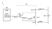
- ⁇ Light-emitting device (first configuration example)> 1 is a diagram showing a first configuration example of a light emitting device.
- the light emitting device 100 of this configuration example includes a semiconductor device 1 and light emitting elements 2(0) to 2(7).
- the light emitting device 100 may be, for example, a head lamp, a tail lamp, a stop lamp, a turn lamp, or an interior lamp (such as an instrument panel lamp) of a vehicle.
- the semiconductor device 1 is a matrix switch IC (bypass switch IC) that switches between short-circuiting and non-shorting each of the light-emitting elements 2(0) to 2(7).
- the semiconductor device 1 also has multiple external terminals (external terminals CH(0) to CH(8) in this figure) as means for establishing electrical connections with the outside of the device.
- Each of the light-emitting elements 2(0) to 2(7) is a series light-emitting element provided on a current path through which the drive current ILED flows.
- each can be understood as a single LED element, or as a light-emitting element assembly in which multiple LED elements are combined in series or in parallel.
- the anode of light-emitting element 2(n) is connected to external terminal CH(n+1) of semiconductor device 1.
- the light emitting device 100 may also include a semiconductor device (a so-called LED driver IC) that generates the above-mentioned drive current ILED.
- a semiconductor device a so-called LED driver IC
- the semiconductor device 1 of this configuration example includes a switch circuit 10 and a control circuit 20 built therein.
- the switch circuit 10 includes switch elements 11(0)-11(7) (in this diagram, NMOSFETs [N-channel type metal oxide semiconductor field effect transistors]), drivers 12(0)-12(7), detection circuits 13(0)-13(7), and level shifters 14(0)-14(7).
- the control circuit 20 also includes PWM [pulse width modulation] dimmer circuits 21(0)-21(7).
- the switch element 11(n) connected in this manner is in an on state when the drive signal VG(n) is at a high level, and in an off state when the drive signal VG(n) is at a low level.
- the driver 12(n) generates the drive signal VG(n) in response to the control signal S4(n) output from the PWM dimming circuit 21(n) (more precisely, the level-shifted control signal S5(n) output from the level shifter 14(n)). For example, the driver 12(n) sets the drive signal VG(n) to a high level when the control signal S4(n) is at a high level, and sets the drive signal VG(n) to a low level when the control signal S4(n) is at a low level.
- the driver 12(n) also has the function of forcibly fixing the logical level of the drive signal VG(n) in response to the detection signal S2(n) output from the detection circuit 13(n).
- Detection circuit 13(n) monitors the voltage across switch element 11(n) and generates detection signals S1(n) and S2(n).
- the voltage across switch element 11(n) is detected as a differential voltage V(n+1)-V(n) between the node voltage V(n) appearing at external terminal CH(n) and the node voltage V(n+1) appearing at external terminal CH(n+1).
- detection signals S1(n) and S2(n) may be the same signal.
- the level shifter 14(n) is provided between the control circuit 20 and the driver 12(n) and detection circuit 13(n).
- the level shifter 14(n) generates a level-shifted control signal S5(n) by shifting the signal level of the control signal S4(n) output from the PWM dimming circuit 21(n).
- the level shifter 14(n) then outputs the level-shifted control signal S5(n) to the driver 12(n).
- the level shifter 14(n) also shifts the signal level of the detection signal S1(n) output from the detection circuit 13(n) to generate a level-shifted detection signal S3(n).
- the level shifter 14(n) then outputs the level-shifted detection signal S3(n) to the control circuit 20.
- the fault detection rate of the semiconductor device 1 is calculated by dividing the element area by the number of elements. Therefore, for example, if a fault in the switch element 11(n), which has a large element area, cannot be detected, a single point fault will occur, and the fault detection rate of the semiconductor device 1 will be significantly reduced.
- First Embodiment 2 is a diagram showing a first embodiment (particularly, a group of components related to fault diagnosis) of the semiconductor device 1.
- a hysteresis comparator is used as the aforementioned detection circuit 13(n).
- the non-inverting input terminal (+) of detection circuit 13(n) is supplied with an added voltage V(n)+Vth(n) obtained by adding the node voltage V(n) appearing at external terminal CH(n) and the threshold voltage Vth(n).
- the inverting input terminal (-) of detection circuit 13(n) is supplied with the node voltage V(n+1) appearing at external terminal CH(n+1).
- the detection signal S1(n) is at a low level when V(n+1)>V(n)+Vth(n) and is at a high level when V(n+1)>V(n)+Vth(n). In other words, the detection signal S1(n) is at a low level when V(n+1)-V(n)>Vth(n) and is at a high level when V(n+1)-V(n) ⁇ Vth(n).
- the detection circuit 13(n) generates the detection signal S1(n) by comparing the voltage V(n+1)-V(n) across the switch element 11(n) with a predetermined threshold voltage Vth(n).
- the threshold voltage Vth(n) is set to a voltage value lower than the forward drop voltage Vf of the light-emitting element 2(n), for example.
- control circuit 20 further includes a fault diagnosis circuit 22(n).
- ⁇ Fault Diagnosis (First Embodiment)> 3 is a diagram showing a first example of fault diagnosis (normal in the first embodiment).
- the drive signal VG(n) the on/off state of the switch element 11(n), the on/off state of the light-emitting element 2(n), the voltage V(n+1)-V(n) across the switch element 11(n), and the detection signal S1(n) are depicted.
- the detection signal S1(n) is at a low level.
- the fault diagnosis circuit 22(n) diagnoses that both the light-emitting element 2(n) and the switch element 11(n) are normal.
- FIG. 4 is a diagram showing a second example of fault diagnosis (when the LED is short-circuited in the first embodiment). As with FIG. 3, this diagram depicts, from top to bottom, the drive signal VG(n), the on/off state of the switch element 11(n), the on/off state of the light-emitting element 2(n), the voltage V(n+1)-V(n) across the switch element 11(n), and the detection signal S1(n).
- FIG. 5 is a diagram showing a third example of fault diagnosis (when SW is stuck on in the first embodiment). As with the above-mentioned FIGS. 3 and 4, this diagram depicts, from top to bottom, the drive signal VG(n), the on/off state of the switch element 11(n), the on/off state of the light-emitting element 2(n), the voltage V(n+1)-V(n) across the switch element 11(n), and the detection signal S1(n).
- the fault diagnosis circuit 22(n) diagnoses that a short circuit has occurred in the light-emitting element 2(n) ( Figure 4) or that the switch element 11(n) is stuck on ( Figure 5).
- FIG. 6 is a diagram showing a fourth example of fault diagnosis (when SW is stuck off in the first embodiment). As with FIGS. 3 to 5, from top to bottom, this diagram depicts the drive signal VG(n), the on/off state of switch element 11(n), the on/off state of light-emitting element 2(n), the voltage V(n+1)-V(n) across switch element 11(n), and the detection signal S1(n).
- the fault diagnosis circuit 22(n) diagnoses that the switch element 11(n) is stuck off when the detection signal S1(n) is at a low level while the drive signal VG(n) is at a high level.
- the fault diagnosis circuit 22(n) can diagnose not only the short circuit of the light-emitting element 2(n) but also whether the switch element 11(n) is stuck on or stuck off.
- the fault detection rate of the semiconductor device 1 is calculated by dividing the element area by the number of elements. Therefore, if a fault in the switch element 11(n), which has a large element area, can be detected, the fault detection rate of the semiconductor device 1 will be significantly improved.
- the conventional LED short detection circuit can be used as is. Therefore, the circuit scale of the semiconductor device 1 does not become unnecessarily large.
- Fault diagnosis circuit 22(n) may output the fault diagnosis result to the outside of semiconductor device 1.
- the fault diagnosis result may be a flag output, or may be read out as register data.
- the host e.g., ECU [electronic control unit]
- the host that receives the fault diagnosis result from the semiconductor device 1 can transition the light emitting device 100 to a safe state in accordance with the fault diagnosis result.
- one possible method for achieving functional safety of the light emitting device 100 is to notify the driver of the occurrence of a fault, for example, by stopping the drive current ILED and turning off all the light emitting elements 2(0) to 2(7).
- Fault diagnosis circuit 22(n) may also transition semiconductor device 1 to a safe state on its own in response to the fault diagnosis result, without waiting for control from the host.
- a possible method for achieving functional safety of semiconductor device 1 is to notify the driver of the occurrence of a fault by, for example, turning all switch elements 11(0)-11(7) on and off in a manner different from normal (all on, all off, blinking or sequential lighting, etc.).
- ⁇ Light-emitting device (second configuration example)> 7 is a diagram showing a second configuration example of a light emitting device.
- the light emitting device 100 of this configuration example includes a semiconductor device 1 and light emitting elements 2(0) to 2(7).
- the cathode of light emitting element 2(n) is connected to an external terminal CH(n) of the semiconductor device 1.
- the anodes of light emitting element 2(n) are all connected to a power supply circuit (not shown). That is, the light emitting elements 2(0) to 2(7) are connected in parallel to the power supply circuit (not shown).
- the semiconductor device 1 includes a switch circuit 10 and a control circuit 20.
- the switch circuit 10 includes current sources 15(0)-15(7) and detection circuits 16(0)-16(7).
- Current source 15(n) is connected in series to light-emitting element 2(n). In this diagram, current source 15(n) is connected between external terminal CH(n) and the ground terminal. Note that current source 15(n) may be replaced with a switch element.
- the current source 15(n) connected in this manner is on/off controlled according to the drive signal S12(n) output from the PWM dimming circuit 21(n) of the control circuit 20.
- the drive current ILED(n) flows through the light-emitting element 2(n). Therefore, the light-emitting element 2(n) is in a light-on state.
- the drive current ILED(n) no longer flows through the light-emitting element 2(n). Therefore, the light-emitting element 2(n) is in a light-off state.
- the node voltage VC(n) can be understood as the cathode voltage of the light-emitting element 2(n).
- the node voltages VC(0) to VC(7) may be output feedback controlled so that the lowest voltage among them matches a predetermined reference voltage Vfb.
- FIG. 8 is a diagram showing a second embodiment of the semiconductor device 1 (particularly, an example of a detection circuit 16(n) used in the light emitting device 100 of the second configuration example (FIG. 7)).
- the detection circuit 16(n) includes comparators 16a(n) and 16b(n).
- the detection circuit 16(n) outputs detection signals S11a(n) and S11b(n) as the aforementioned detection signal S11(n).
- Comparator 16a(n) outputs detection signal S11a(n) by comparing node voltage VC(n) input to the non-inverting input terminal (+) with threshold voltage Vth1 input to the inverting input terminal (-). Therefore, detection signal S11a(n) is at high level when VC(n)>Vth1, and is at low level when VC(n) ⁇ Vth1.
- threshold voltage Vth1 corresponds to the short circuit detection voltage of light-emitting element 2(n).
- Threshold voltage Vth1 is set to a voltage value higher than reference voltage Vfb.
- Comparator 16b(n) outputs detection signal S11b(n) by comparing node voltage VC(n) input to the inverting input terminal (-) with threshold voltage Vth2 input to the non-inverting input terminal (+). Therefore, detection signal S11b(n) is at low level when VC(n)>Vth2, and at high level when VC(n) ⁇ Vth2.
- threshold voltage Vth2 corresponds to the open detection voltage of light-emitting element 2(n).
- Threshold voltage Vth2 is set to a voltage value lower than reference voltage Vfb.
- the fault diagnosis circuit 22(n) monitors the detection signals S11a(n) and S11b(n) when the drive signal S12(n) of the current source 15(n) is at the on-logic level, and performs short circuit and open circuit diagnosis of the light-emitting element 2(n).
- the fault diagnosis circuit 22(n) monitors at least one of the detection signals S11a(n) and S11b(n) when the drive signal S12(n) of the current source 15(n) is at the off logic level, and performs a stuck-on diagnosis or a stuck-off diagnosis of the current source 15(n).
- Current source 15(n) stuck on (hereinafter sometimes referred to as CS stuck on) refers to a failure mode in which current source 15(n) does not turn off and remains on even though the drive signal S12(n) of current source 15(n) is set to the off logical level.
- Current source 15(n) stuck off (hereinafter sometimes referred to as CS stuck off) refers to a failure mode in which current source 15(n) does not turn on and remains in the off state even though the drive signal S12(n) for current source 15(n) is set to the on logical level.
- ⁇ Fault Diagnosis (Second Embodiment)> 9 is a diagram showing a fifth example of fault diagnosis (normal in the second embodiment).
- the drive signal S12(n) of the current source 15(n) the on/off state of the light-emitting element 2(n), the node voltage VC(n), and the detection signals S11a(n) and S11b(n) are depicted.
- the light-emitting element 2(n) and the current source 15(n) are normal, if the drive signal S12(n) of the current source 15(n) is at the off logical level, the current source 15(n) is in the off state. At this time, the drive current ILED does not flow through the light-emitting element 2(n). Therefore, the light-emitting element 2(n) is in the off state.
- the node voltage VC(n) is higher than the threshold voltage Vth1. In other words, Vth2 ⁇ Vth1 ⁇ VC(n) is established. Therefore, the detection signal S11a(n) is at a high level, and the detection signal S11b(n) is at a low level.
- the fault diagnosis circuit 22(n) diagnoses that both the light-emitting element 2(n) and the current source 15(n) are normal when the detection signals S11a(n) and S11b(n) are both at a low level when the drive signal S12(n) is at an on-logic level, and when the detection signal S11a(n) is at a high level and the detection signal S11b(n) is at a low level when the drive signal S12(n) is at an off-logic level.
- FIG. 10 is a diagram showing a sixth example of fault diagnosis (when the LED is short-circuited in the second embodiment). As with FIG. 9, this diagram depicts the drive signal S12(n) of the current source 15(n), the on/off state of the light-emitting element 2(n), the node voltage VC(n), and the detection signals S11a(n) and S11b(n).
- the fault diagnosis circuit 22(n) diagnoses that a short circuit has occurred in the light-emitting element 2(n).
- FIG. 11 is a diagram showing a seventh example of fault diagnosis (when the LED is open in the second embodiment). Note that, like the above-mentioned FIGS. 9 and 10, this diagram depicts the drive signal S12(n) of the current source 15(n), the on/off state of the light-emitting element 2(n), the node voltage VC(n), and the detection signals S11a(n) and S11b(n).
- the node voltage VC(n) is lower than the threshold voltage Vth2. In other words, VC(n) ⁇ Vth2 ⁇ Vth1 is established. Therefore, the detection signal S11a(n) is at a low level, and the detection signal S11b(n) is at a high level.
- the fault diagnosis circuit 22(n) diagnoses that an open circuit has occurred in the light-emitting element 2(n).
- the fault diagnosis circuit 22(n) diagnoses that the current source 15(n) is stuck on when the detection signal S11a(n) is at a low level at the timing when the drive signal S12(n) is at its off logical level.
- FIG. 14 is a diagram showing a third embodiment of the semiconductor device 1 (particularly a specific example of the current source 15(n) and a modified example of the detection circuit 16(n) used in the light emitting device 100 of the second configuration example (FIG. 7)).
- the current source 15(n) includes a transistor 15a(n) (an NMOSFET in the example shown in the figure), a resistor 15b(n), and an amplifier 15c(n).
- the detection circuit 16(n) includes a comparator 16c(n).
- the detection circuit 16(n) outputs a detection signal S11c(n) as the aforementioned detection signal S11(n).
- the drain of the transistor 15a(n) is connected to the external terminal CH(n).
- the source of the transistor 15a(n) is connected to the first terminal of the resistor 15b(n).
- the second terminal of the resistor 15b(n) is connected to the ground terminal.
- the reference voltage Vref may be adjustable using a DAC [digital-to-analog converter] or the like.
- Comparator 16c(n) outputs detection signal S11c(n) by comparing sense voltage Vs(n) input to the inverting input terminal (-) with threshold voltage Vth3 input to the non-inverting input terminal (+). Therefore, detection signal S11c(n) is at low level when Vs(n)>Vth3, and at high level when Vs(n) ⁇ Vth3.
- the fault diagnosis circuit 22(n) performs a stuck-on diagnosis or a stuck-off diagnosis of the current source 15(n) by monitoring the detection signal S11c(n) both when the drive signal S12(n) of the current source 15(n) is at the off logic level and when it is at the on logic level.
- ⁇ Fault Diagnosis (Third Embodiment)> 15 is a diagram showing a tenth example of fault diagnosis (normal in the third embodiment). In this diagram, from the top, the drive signal S12(n) of the current source 15(n), the on/off state of the light-emitting element 2(n), the sense voltage Vs(n), and the detection signal S11c(n) are depicted.
- the drive signal S12(n) of the current source 15(n) is at the off logical level
- the current source 15(n) is in the off state.
- the drive current ILED does not flow to the light-emitting element 2(n). Therefore, the light-emitting element 2(n) is in the off state.
- the sense voltage Vs(n) becomes lower than the threshold voltage Vth3. Therefore, the detection signal S11c(n) becomes high level.
- the fault diagnosis circuit 22(n) diagnoses that both the light-emitting element 2(n) and the current source 15(n) are normal.
- FIG. 16 is a diagram showing an eleventh example of fault diagnosis (when CS is stuck on in the third embodiment). As with FIG. 15, from the top, this diagram depicts the drive signal S12(n) of the current source 15(n), the on/off state of the light-emitting element 2(n), the sense voltage Vs(n), and the detection signal S11c(n).
- the fault diagnosis circuit 22(n) diagnoses that the current source 15(n) is stuck on when the detection signal S11c(n) is at a low level at the timing when the drive signal S12(n) is at its off logical level.
- FIG. 17 is a diagram showing a twelfth example of fault diagnosis (when CS is stuck off in the third embodiment). As with the above-mentioned FIGS. 15 and 16, this diagram depicts, from top to bottom, the drive signal S12(n) of the current source 15(n), the on/off state of the light-emitting element 2(n), the sense voltage Vs(n), and the detection signal S11c(n).
- the fault diagnosis circuit 22(n) diagnoses that the current source 15(n) is stuck off when the detection signal S11c(n) is at a high level at the timing when the drive signal S12(n) is at the on logical level.
- the second embodiment (FIG. 8) and the third embodiment (FIG. 14) may be combined. By combining the two detection methods, it becomes possible to correctly diagnose the failure mode of each of the light-emitting element 2(n) and the current source 15(n).
- ⁇ Application to vehicles> 18 and 19 are diagrams showing the external appearance (front and rear) of a vehicle on which the above-mentioned light-emitting device 100 can be mounted.
- the light-emitting device 100 can be suitably used, for example, as a headlamp (including high beam/low beam/small lamp/fog lamp, etc., as appropriate) X11, a daytime running lamp (DRL [daylight running lamps]) X12, a tail lamp (including small lamp or back lamp, etc., as appropriate) X13, a stop lamp X14, and a turn lamp X15 of the vehicle X10.
- the light-emitting device 100 may be an interior lamp (such as an instrument panel lamp) of the vehicle X10.
- the semiconductor device disclosed in this specification is configured (first configuration) to include a switch element configured to be connected in parallel to a light-emitting element, a detection circuit configured to generate a detection signal by comparing the voltage across the switch element with a predetermined threshold voltage, and a fault diagnosis circuit configured to diagnose whether the switch element is stuck off by monitoring the detection signal at a timing when the drive signal for the switch element is at an on-logic level.
- the fault diagnosis circuit may be configured (second configuration) to diagnose whether the switch element is stuck on or whether the light-emitting element to which the switch element is connected in parallel is short-circuited by monitoring the detection signal at a timing when the drive signal is at an off logic level.
- the fault diagnosis circuit may be configured to output the fault diagnosis result to the outside of the semiconductor device (third configuration).
- the fault diagnosis circuit may be configured to transition the semiconductor device to a safe state (fourth configuration).
- a semiconductor device may be further configured (fifth configuration) to include a control circuit configured to generate a control signal, and a driver configured to generate the drive signal in response to the control signal.
- the semiconductor device according to the fifth configuration may be further configured (sixth configuration) to include a level shifter configured to shift the signal level of the control signal between the control circuit and the driver.
- the semiconductor device disclosed in this specification is configured (seventh configuration) to include a switch element or a current source configured to be connected in series to a light-emitting element, a detection circuit configured to generate a detection signal by comparing the voltage across the switch element or the current source with a predetermined threshold voltage, and a fault diagnosis circuit configured to diagnose whether the switch element or the current source is stuck on by monitoring the detection signal at a timing when the drive signal for the switch element or the current source is at an off logic level.
- the fault diagnosis circuit may be configured (eighth configuration) to perform a stuck-off diagnosis of the switch element or the current source, or a short circuit diagnosis or open circuit diagnosis of the light-emitting element by monitoring the detection signal at the timing when the drive signal is at the on-logic level.
- the semiconductor device disclosed in this specification is configured (ninth configuration) to include a switch element or a current source configured to be connected in series to a light-emitting element, a detection circuit configured to detect a drive current flowing through the switch element or the current source and generate a detection signal, and a fault diagnosis circuit configured to diagnose whether the switch element or the current source is stuck on by monitoring the detection signal when the drive signal of the switch element or the current source is at a logical level when it is off, and to diagnose whether the switch element or the current source is stuck off by monitoring the detection signal when the drive signal of the switch element or the current source is at a logical level when it is on.
- the light emitting device disclosed in this specification has a configuration (tenth configuration) including the light emitting element and a semiconductor device having any one of the first to ninth configurations described above.
- the light-emitting device may also be configured (eleventh configuration) in which the light-emitting element is an LED element or an organic EL element.
- the vehicle disclosed in this specification is configured to include a light-emitting device according to the tenth or eleventh configuration (twelfth configuration).
Landscapes
- Electronic Switches (AREA)
- Engineering & Computer Science (AREA)
- Mechanical Engineering (AREA)
Abstract
半導体装置1は、発光素子2(n)に対して並列に接続されるスイッチ素子11(n)と、スイッチ素子11(n)の両端間電圧V(n+1)-V(n)と所定の閾値電圧Vthとを比較して検出信号S1(n)を生成する検出回路13(n)と、スイッチ素子11(n)の駆動信号VG(n)がオン時の論理レベルとされているタイミングで検出信号S1(n)を監視することによりスイッチ素子11(n)のオフ固着診断を行う故障診断回路22(n)と、を備える。
Description
本開示は、半導体装置、及び、これを用いた発光装置並びに車両に関する。
LED[light emitting diode]素子などの発光素子を点灯/消灯する半導体装置(例えばマトリクススイッチIC[integrated circuit]又はバイパススイッチIC)には、発光素子の故障(短絡など)を検出するための検出回路が内蔵されている。
なお、上記に関連する従来技術の一例としては、特許文献1を挙げることができる。
しかしながら、従来の半導体装置は、故障検出率の向上について検討の余地があった。
例えば、本明細書中に開示されている半導体装置は、発光素子に対して並列に接続されるように構成されたスイッチ素子と、前記スイッチ素子の両端間電圧と所定の閾値電圧とを比較して検出信号を生成するように構成された検出回路と、前記スイッチ素子の駆動信号がオン時の論理レベルとされているタイミングで前記検出信号を監視することにより前記スイッチ素子のオフ固着診断を行うように構成された故障診断回路と、を備える。
また、例えば、本明細書中に開示されている半導体装置は、発光素子に対して直列に接続されるように構成されたスイッチ素子又は電流源と、前記スイッチ素子又は前記電流源の両端間電圧と所定の閾値電圧とを比較して検出信号を生成するように構成された検出回路と、前記スイッチ素子又は前記電流源の駆動信号がオフ時の論理レベルとされているタイミングで前記検出信号を監視することにより前記スイッチ素子又は前記電流源のオン固着診断を行うように構成された故障診断回路と、を備える。
また、例えば、本明細書中に開示されている半導体装置は、発光素子に対して直列に接続されるように構成されたスイッチ素子又は電流源と、前記スイッチ素子又は前記電流源に流れる駆動電流を検出するように構成された検出回路と、前記スイッチ素子又は前記電流源の駆動信号がオフ時の論理レベルとされているタイミングで前記検出信号を監視することにより前記スイッチ素子又は前記電流源のオン固着診断を行い、前記スイッチ素子又は前記電流源の駆動信号がオン時の論理レベルとされているタイミングで前記検出信号を監視することにより前記スイッチ素子又は前記電流源のオフ固着診断を行うように構成された故障診断回路と、を備える。
なお、その他の特徴、要素、ステップ、利点、及び、特性については、以下に続く発明を実施するための形態及びこれに関する添付の図面によって、さらに明らかとなる。
本開示によれば、故障検出率を高めることのできる半導体装置、及び、これを用いた発光装置並びに車両を提供することが可能となる。
<発光装置(第1構成例)>
図1は、発光装置の第1構成例を示す図である。本構成例の発光装置100は、半導体装置1と、発光素子2(0)~2(7)と、を備える。発光装置100は、例えば、車両のヘッドランプ、テールランプ、ストップランプ、ターンランプ、又は、室内ランプ(インパネランプなど)であってもよい。
図1は、発光装置の第1構成例を示す図である。本構成例の発光装置100は、半導体装置1と、発光素子2(0)~2(7)と、を備える。発光装置100は、例えば、車両のヘッドランプ、テールランプ、ストップランプ、ターンランプ、又は、室内ランプ(インパネランプなど)であってもよい。
半導体装置1は、発光素子2(0)~2(7)それぞれの短絡/非短絡を切り替えるマトリクススイッチIC(バイパススイッチIC)である。なお、半導体装置1は、装置外部との電気的な接続を確立するための手段として複数の外部端子(本図では外部端子CH(0)~CH(8))を備えている。
発光素子2(0)~2(7)は、それぞれ、駆動電流ILEDの流れる電流経路上に設けられた直列発光体である。発光素子2(0)~2(7)を個別に見た場合、それぞれを単一のLED素子として理解することもできるし、或いは、複数のLED素子を直列又は並列に組み合わせた発光素子集合体として理解することもできる。
なお、発光素子2(n)(ただしn=0,1,…,7、以下も同様)のカソードは、半導体装置1の外部端子CH(n)に接続されている。一方、発光素子2(n)のアノードは、半導体装置1の外部端子CH(n+1)に接続されている。
また、本図では明示されていないが、発光装置100は、上記の駆動電流ILEDを生成する半導体装置(いわゆるLEDドライバIC)を備えていてもよい。
<半導体装置>
引き続き、図1を参照しながら半導体装置1の内部構成について説明する。本構成例の半導体装置1には、スイッチ回路10と制御回路20が内蔵されている。
引き続き、図1を参照しながら半導体装置1の内部構成について説明する。本構成例の半導体装置1には、スイッチ回路10と制御回路20が内蔵されている。
スイッチ回路10は、スイッチ素子11(0)~11(7)(本図では、NMOSFET[N-channel type metal oxide semiconductor field effect transistor])と、ドライバ12(0)~12(7)と、検出回路13(0)~13(7)と、レベルシフタ14(0)~14(7)を含む。また、制御回路20は、PWM[pulse width modulation]調光回路21(0)~21(7)を含む。
スイッチ素子11(n)は、発光素子2(n)に対して並列に接続されている。本図に即して具体的に述べると、スイッチ素子11(n)のソースは、外部端子CH(n)に接続されている。スイッチ素子11(n)のドレインは、外部端子CH(n+1)に接続されている。スイッチ素子11(n)のゲートは、駆動信号VG(n)の印加端(=ドライバ12(n)の出力端)に接続されている。
このように接続されたスイッチ素子11(n)は、駆動信号VG(n)がハイレベルであるときにオン状態となり、駆動信号VG(n)がローレベルであるときにオフ状態となる。なお、スイッチ素子11(n)がオン状態であるときには、発光素子2(n)の両端間が短絡状態となる。従って、発光素子2(n)が消灯状態(=点灯不能状態)となる。一方、スイッチ素子11(n)がオフ状態であるときには、発光素子2(n)の両端間が非短絡状態となる。従って、発光素子2(n)が点灯状態(=点灯可能状態)となる。
ドライバ12(n)は、PWM調光回路21(n)から出力される制御信号S4(n)(より正確には、レベルシフタ14(n)から出力されるレベルシフト済みの制御信号S5(n))に応じて駆動信号VG(n)を生成する。例えば、ドライバ12(n)は、制御信号S4(n)がハイレベルであるときに駆動信号VG(n)をハイレベルとし、制御信号S4(n)がローレベルであるときに駆動信号VG(n)をローレベルとする。
また、ドライバ12(n)は、検出回路13(n)から出力される検出信号S2(n)に応じて駆動信号VG(n)の論理レベルを強制的に固定する機能も備えている。
検出回路13(n)は、スイッチ素子11(n)の両端間電圧を監視して検出信号S1(n)及びS2(n)を生成する。スイッチ素子11(n)の両端間電圧は、外部端子CH(n)に現れるノード電圧V(n)と、外部端子CH(n+1)に現れるノード電圧V(n+1)との差分電圧V(n+1)-V(n)として検出される。なお、検出信号S1(n)及びS2(n)は、同一信号であってもよい。
レベルシフタ14(n)は、制御回路20と、ドライバ12(n)および検出回路13(n)との間に設けられている。レベルシフタ14(n)は、PWM調光回路21(n)から出力される制御信号S4(n)の信号レベルをシフトさせることによりレベルシフト済みの制御信号S5(n)を生成する。そして、レベルシフタ14(n)は、レベルシフト済みの制御信号S5(n)をドライバ12(n)に出力する。また、レベルシフタ14(n)は、検出回路13(n)から出力される検出信号S1(n)の信号レベルをシフトさせることによりレベルシフト済みの検出信号S3(n)を生成する。そして、レベルシフタ14(n)は、レベルシフト済みの検出信号S3(n)を制御回路20に出力する。
PWM調光回路21(n)は、発光素子2(n)の輝度に応じたオンデューティDon(=パルス周期に対するオン期間の比率)の制御信号S4(n)を生成する。先にも述べたように、発光素子2(n)は、スイッチ素子11(n)がオン状態であるときに消灯状態(=点灯不能状態)となり、スイッチ素子11(n)がオフ状態であるときに点灯状態(=点灯可能状態)となる。従って、発光素子2(n)をフル点灯(輝度100%)すべきときには、制御信号S4(n)のオンデューティDonが0%(常にローレベル)に設定される。一方、発光素子2(n)を消灯すべきときには、制御信号S4(n)のオンデューティDonが100%(常にハイレベル)に設定される。
<故障検出率に関する考察>
ところで、半導体装置1が車載用途である場合には、機能安全に関する厳しい国際規格を満たさなければならない。例えば、上記国際規格の一つであるISO[international organization for standardization]26262に準拠するためには、故障モード影響診断解析(いわゆるFMEDA[failure modes effects and diagnostics analysis])による半導体装置1の故障分析が必要となる。
ところで、半導体装置1が車載用途である場合には、機能安全に関する厳しい国際規格を満たさなければならない。例えば、上記国際規格の一つであるISO[international organization for standardization]26262に準拠するためには、故障モード影響診断解析(いわゆるFMEDA[failure modes effects and diagnostics analysis])による半導体装置1の故障分析が必要となる。
そのためには、システムで要求される安全レベルに応じて、半導体装置1に外付けされる発光素子2(n)の故障検出(LED短絡検出)を行うだけでなく、半導体装置1に内蔵される内部素子及び内部回路の故障検出率を高める必要がある。
なお、半導体装置1の故障検出率は、素子面積の案分で算出される。従って、例えば、素子面積の大きいスイッチ素子11(n)の故障が検出できなければ、シングルポイントフォールトとなり、半導体装置1の故障検出率が大きく低下してしまう。
以下では、上記の考察に鑑み、半導体装置1の故障検出率を高めることのできる新規な実施形態を提案する。
<半導体装置(第1実施形態)>
図2は、半導体装置1の第1実施形態(特に故障診断に関連する構成要素群)を示す図である。本実施形態の半導体装置1では、先出の検出回路13(n)としてヒステリシスコンパレータが用いられている。
図2は、半導体装置1の第1実施形態(特に故障診断に関連する構成要素群)を示す図である。本実施形態の半導体装置1では、先出の検出回路13(n)としてヒステリシスコンパレータが用いられている。
本図に即して述べると、検出回路13(n)の非反転入力端(+)には、外部端子CH(n)に現れるノード電圧V(n)と閾値電圧Vth(n)とを足し合わせた加算電圧V(n)+Vth(n)が入力されている。一方、検出回路13(n)の反転入力端(-)には、外部端子CH(n+1)に現れるノード電圧V(n+1)が入力されている。
従って、検出信号S1(n)は、V(n+1)>V(n)+Vth(n)であるときにローレベルとなり、V(n+1)>V(n)+Vth(n)であるときにハイレベルとなる。言い換えると、検出信号S1(n)は、V(n+1)-V(n)>Vth(n)であるときにローレベルとなり、V(n+1)-V(n)<Vth(n)であるときにハイレベルとなる。
上記したように、検出回路13(n)は、スイッチ素子11(n)の両端間電圧V(n+1)-V(n)と所定の閾値電圧Vth(n)とを比較することにより、検出信号S1(n)を生成する。閾値電圧Vth(n)は、例えば、発光素子2(n)の順方向降下電圧Vfよりも低い電圧値に設定されている。
また、本実施形態の半導体装置1において、制御回路20は、故障診断回路22(n)をさらに含む。
故障診断回路22(n)は、スイッチ素子11(n)の駆動信号VG(n)がローレベル(=オフ時の論理レベル)とされているタイミングで検出信号S1(n)を監視することによりスイッチ素子11(n)のオン固着診断又はスイッチ素子11(n)が並列に接続された発光素子2(n)の短絡診断を行う。
スイッチ素子11(n)のオン固着(以下ではSWオン固着と呼ぶことがある)とは、スイッチ素子11(n)の駆動信号VG(n)がローレベル(=オフ時の論理レベル)とされているにも関わらず、スイッチ素子11(n)がオフ状態とならず、オン状態に維持される故障モードのことを言う。
また、故障診断回路22(n)は、スイッチ素子11(n)の駆動信号VG(n)がハイレベル(=オン時の論理レベル)とされているタイミングで検出信号S1(n)を監視することによりスイッチ素子11(n)のオフ固着診断を行う。
スイッチ素子11(n)のオフ固着(以下ではSWオフ固着と呼ぶことがある)とは、スイッチ素子11(n)の駆動信号VG(n)がハイレベル(=オン時の論理レベル)とされているにも関わらず、スイッチ素子11(n)がオン状態とならず、オフ状態に維持される故障モードのことを言う。
<故障診断(第1実施形態)>
図3は、故障診断の第1例(第1実施形態における正常時)を示す図である。なお、本図では、上から順に、駆動信号VG(n)、スイッチ素子11(n)のオン/オフ状態、発光素子2(n)の点灯/消灯状態、スイッチ素子11(n)の両端間電圧V(n+1)-V(n)、及び、検出信号S1(n)が描写されている。
図3は、故障診断の第1例(第1実施形態における正常時)を示す図である。なお、本図では、上から順に、駆動信号VG(n)、スイッチ素子11(n)のオン/オフ状態、発光素子2(n)の点灯/消灯状態、スイッチ素子11(n)の両端間電圧V(n+1)-V(n)、及び、検出信号S1(n)が描写されている。
発光素子2(n)及びスイッチ素子11(n)のいずれにも故障が生じていない正常時において、駆動信号VG(n)がハイレベルであるときには、スイッチ素子11(n)がオン状態となる。このとき、発光素子2(n)がスイッチ素子11(n)によってバイパスされるので、発光素子2(n)には駆動電流ILEDが流れなくなる。従って、発光素子2(n)が消灯状態(=点灯不能状態)となる。また、スイッチ素子11(n)がオン状態であるときには、スイッチ素子11(n)の両端間電圧V(n+1)-V(n)が0V(<Vth(n))となる。従って、検出信号S1(n)がハイレベルとなる。
また、発光素子2(n)及びスイッチ素子11(n)の正常時において、駆動信号VG(n)がローレベルであるときには、スイッチ素子11(n)がオフ状態となる。このとき、スイッチ素子11(n)による発光素子2(n)のバイパスが解除されるので、発光素子2(n)に駆動電流ILEDが流れる。従って、発光素子2(n)が点灯状態(=点灯可能状態)となる。また、スイッチ素子11(n)がオフ状態であるときには、スイッチ素子11(n)の両端間電圧V(n+1)-V(n)が発光素子2(n)の順方向降下電圧Vf(>Vth(n))となる。従って、検出信号S1(n)がローレベルとなる。
図3の挙動に鑑み、故障診断回路22(n)は、駆動信号VG(n)がハイレベルであるときに検出信号S1(n)がハイレベルであって、かつ、駆動信号VG(n)がローレベルであるときに検出信号S1(n)がローレベルであるときには、発光素子2(n)及びスイッチ素子11(n)がいずれも正常であると診断する。
図4は、故障診断の第2例(第1実施形態におけるLED短絡時)を示す図である。なお、本図では、先出の図3と同様、上から順に、駆動信号VG(n)、スイッチ素子11(n)のオン/オフ状態、発光素子2(n)の点灯/消灯状態、スイッチ素子11(n)の両端間電圧V(n+1)-V(n)、及び、検出信号S1(n)が描写されている。
発光素子2(n)のアノードとカソードとの間が短絡しているときには、駆動信号VG(n)がローレベルとされて、スイッチ素子11(n)がオフ状態となっても、発光素子2(n)に駆動電流ILEDが流れない。従って、発光素子2(n)が消灯状態(=点灯不能状態)となる。また、発光素子2(n)に順方向降下電圧Vfが生じないので、スイッチ素子11(n)の両端間電圧V(n+1)-V(n)が閾値電圧Vth(n)よりも低くなる。従って、検出信号S1(n)がハイレベルとなる。
図5は、故障診断の第3例(第1実施形態におけるSWオン固着時)を示す図である。なお、本図では、先出の図3及び図4と同じく、上から順に、駆動信号VG(n)、スイッチ素子11(n)のオン/オフ状態、発光素子2(n)の点灯/消灯状態、スイッチ素子11(n)の両端間電圧V(n+1)-V(n)、及び、検出信号S1(n)が描写されている。
スイッチ素子11(n)がオン固着しているときには、駆動信号VG(n)がローレベルとされても、スイッチ素子11(n)がオフ状態とならずにオン状態のままとなる。そのため、発光素子2(n)がスイッチ素子11(n)によりバイパスされるので、発光素子2(n)には駆動電流ILEDが流れなくなる。従って、発光素子2(n)が消灯状態(=点灯不能状態)となる。また、スイッチ素子11(n)がオン状態であるときには、スイッチ素子11(n)の両端間電圧V(n+1)-V(n)が0V(<Vth(n))となる。従って、検出信号S1(n)がハイレベルとなる。
図4及び図5の挙動に鑑み、故障診断回路22(n)は、駆動信号VG(n)のローレベル期間に検出信号S1(n)がハイレベルとなっているときには、発光素子2(n)の短絡(図4)又はスイッチ素子11(n)のオン固着(図5)が生じていると診断する。
図6は、故障診断の第4例(第1実施形態におけるSWオフ固着時)を示す図である。本図では、先の図3~図5と同様、上から順に、駆動信号VG(n)、スイッチ素子11(n)のオン/オフ状態、発光素子2(n)の点灯/消灯状態、スイッチ素子11(n)の両端間電圧V(n+1)-V(n)、及び、検出信号S1(n)が描写されている。
スイッチ素子11(n)がオフ固着しているときには、駆動信号VG(n)がハイレベルとされても、スイッチ素子11(n)がオン状態とならずにオフ状態のままとなる。そのため、発光素子2(n)がバイパスされないので、発光素子2(n)に駆動電流ILEDが流れる。従って、発光素子2(n)が点灯状態(=消灯不能状態)となる。また、スイッチ素子11(n)がオフ状態であるときには、スイッチ素子11(n)の両端間電圧V(n+1)-V(n)が発光素子2(n)の順方向降下電圧Vf(>Vth(n))となる。従って、検出信号S1(n)がローレベルとなる。
図6の挙動に鑑み、故障診断回路22(n)は、駆動信号VG(n)のハイレベル期間に検出信号S1(n)がローレベルとなっているときには、スイッチ素子11(n)のオフ固着が生じていると診断する。
このように、故障診断回路22(n)は、発光素子2(n)の短絡診断だけでなく、スイッチ素子11(n)のオン固着及びオフ固着を診断することができる。
先にも述べたように、半導体装置1の故障検出率は、素子面積の案分で算出される。従って、素子面積の大きいスイッチ素子11(n)の故障が検出できれば、半導体装置1の故障検出率が大きく向上する。
また、検出回路13(n)については、従前のLEDショート検出回路がそのまま流用可能である。従って、半導体装置1の回路規模が不必要に大きくならない。
なお、故障診断回路22(n)は、故障診断結果を半導体装置1の外部に出力してもよい。例えば、故障診断結果は、フラグ出力であってもよいし、或いは、レジスタデータとして読み出されてもよい。
このような構成であれば、半導体装置1から故障診断結果を受けたホスト(例えばECU[electronic control unit])は、故障診断結果に応じて発光装置100を安全状態に移行することができる。なお、発光装置100の機能安全を実現するための手法としては、例えば、駆動電流ILEDを停止して全ての発光素子2(0)~2(7)を消灯させることにより、運転者に故障の発生を通知することが考えられる。
また、故障診断回路22(n)は、ホストからの制御を待つことなく、故障診断結果に応じて自らで半導体装置1を安全状態に移行してもよい。なお、半導体装置1の機能安全を実現するための手法としては、例えば、全てのスイッチ素子11(0)~11(7)を通常時とは異なる挙動で点消灯(全点灯、全消灯、点滅又はシーケンシャル点灯など)させることにより、運転者に故障の発生を通知することが考えられる。
<発光装置(第2構成例)>
図7は、発光装置の第2構成例を示す図である。本構成例の発光装置100は、半導体装置1と、発光素子2(0)~2(7)と、を備える。なお、発光素子2(n)のカソードは、半導体装置1の外部端子CH(n)に接続されている。一方、発光素子2(n)のアノードは、いずれも不図示の電源回路に接続されている。すなわち、発光素子2(0)~2(7)は、不図示の電源回路に対して並列に接続されている。
図7は、発光装置の第2構成例を示す図である。本構成例の発光装置100は、半導体装置1と、発光素子2(0)~2(7)と、を備える。なお、発光素子2(n)のカソードは、半導体装置1の外部端子CH(n)に接続されている。一方、発光素子2(n)のアノードは、いずれも不図示の電源回路に接続されている。すなわち、発光素子2(0)~2(7)は、不図示の電源回路に対して並列に接続されている。
半導体装置1には、スイッチ回路10と制御回路20が内蔵されている。スイッチ回路10は、電流源15(0)~15(7)と、検出回路16(0)~16(7)とを含む。
電流源15(n)は、発光素子2(n)に対して直列に接続されている。本図に即して述べると、電流源15(n)は、外部端子CH(n)と接地端との間に接続されている。なお、電流源15(n)は、スイッチ素子に置き換えられてもよい。
このように接続された電流源15(n)は、制御回路20のPWM調光回路21(n)から出力される駆動信号S12(n)に応じてオン/オフ制御される。電流源15(n)がオン状態であるときには、発光素子2(n)に駆動電流ILED(n)が流れる。従って、発光素子2(n)が点灯状態となる。一方、電流源15(n)がオフ状態であるときには、発光素子2(n)に駆動電流ILED(n)が流れなくなる。従って、発光素子2(n)が消灯状態となる。
検出回路16(n)は、電流源15(n)の両端間電圧(=外部端子CH(n)に印加されるノード電圧VC(n))を監視して検出信号S11(n)を生成する。なお、ノード電圧VC(n)は、発光素子2(n)のカソード電圧として理解され得る。
なお、ノード電圧VC(0)~VC(7)は、そのうちで最も低い電圧が所定の基準電圧Vfbと一致するように出力帰還制御されてもよい。
<半導体装置(第2実施形態)>
図8は、半導体装置1の第2実施形態(特に第2構成例(図7)の発光装置100に用いられる検出回路16(n)の一例)を示す図である。本実施形態の半導体装置1において、検出回路16(n)は、コンパレータ16a(n)及び16b(n)を含む。なお、検出回路16(n)は、先出の検出信号S11(n)として、検出信号S11a(n)及びS11b(n)を出力する。
図8は、半導体装置1の第2実施形態(特に第2構成例(図7)の発光装置100に用いられる検出回路16(n)の一例)を示す図である。本実施形態の半導体装置1において、検出回路16(n)は、コンパレータ16a(n)及び16b(n)を含む。なお、検出回路16(n)は、先出の検出信号S11(n)として、検出信号S11a(n)及びS11b(n)を出力する。
コンパレータ16a(n)は、非反転入力端(+)に入力されるノード電圧VC(n)と、反転入力端(-)に入力される閾値電圧Vth1とを比較することにより、検出信号S11a(n)を出力する。従って、検出信号S11a(n)は、VC(n)>Vth1であるときにハイレベルとなり、VC(n)<Vth1であるときにローレベルとなる。なお、閾値電圧Vth1は、発光素子2(n)の短絡検出電圧に相当する。閾値電圧Vth1は、基準電圧Vfbよりも高い電圧値に設定される。
コンパレータ16b(n)は、反転入力端(-)に入力されるノード電圧VC(n)と非反転入力端(+)に入力される閾値電圧Vth2とを比較することにより、検出信号S11b(n)を出力する。従って、検出信号S11b(n)は、VC(n)>Vth2であるときにローレベルとなり、VC(n)<Vth2であるときにハイレベルとなる。なお、閾値電圧Vth2は、発光素子2(n)のオープン検出電圧に相当する。閾値電圧Vth2は、基準電圧Vfbよりも低い電圧値に設定される。
故障診断回路22(n)は、電流源15(n)の駆動信号S12(n)がオン時の論理レベルとされているタイミングで検出信号S11a(n)及びS11b(n)をそれぞれ監視して発光素子2(n)の短絡診断及びオープン診断を行う。
また、故障診断回路22(n)は、電流源15(n)の駆動信号S12(n)がオフ時の論理レベルとされているタイミングで検出信号S11a(n)及びS11b(n)の少なくとも一方を監視して電流源15(n)のオン固着診断又はオフ固着診断を行う。
電流源15(n)のオン固着(以下ではCSオン固着と呼ぶことがある)とは、電流源15(n)の駆動信号S12(n)がオフ時の論理レベルとされているにも関わらず、電流源15(n)がオフ状態とならず、オン状態に維持される故障モードのことを言う。
電流源15(n)のオフ固着(以下ではCSオフ固着と呼ぶことがある)とは、電流源15(n)の駆動信号S12(n)がオン時の論理レベルとされているにも関わらず、電流源15(n)がオン状態とならず、オフ状態に維持される故障モードのことを言う。
<故障診断(第2実施形態)>
図9は、故障診断の第5例(第2実施形態における正常時)を示す図である。なお、本図では、上から順番に、電流源15(n)の駆動信号S12(n)、発光素子2(n)の点灯/消灯状態、ノード電圧VC(n)、及び、検出信号S11a(n)並びにS11b(n)が描写されている。
図9は、故障診断の第5例(第2実施形態における正常時)を示す図である。なお、本図では、上から順番に、電流源15(n)の駆動信号S12(n)、発光素子2(n)の点灯/消灯状態、ノード電圧VC(n)、及び、検出信号S11a(n)並びにS11b(n)が描写されている。
発光素子2(n)及び電流源15(n)のいずれにも故障が生じていない正常時において、電流源15(n)の駆動信号S12(n)がオン時の論理レベルであるときには、電流源15(n)がオン状態となる。このとき、発光素子2(n)に駆動電流ILEDが流れる。従って、発光素子2(n)が点灯状態となる。また、電流源15(n)がオン状態であるときには、ノード電圧VC(n)が基準電圧Vfbと同値又は基準電圧Vfbの近傍値となる。すなわち、Vth2<VC(n)<Vth1が成立する。従って、検出信号S11a(n)及びS11b(n)がいずれもローレベルとなる。
また、発光素子2(n)及び電流源15(n)の正常時において、電流源15(n)の駆動信号S12(n)がオフ時の論理レベルであるときには、電流源15(n)がオフ状態となる。このとき、発光素子2(n)には駆動電流ILEDが流れない。従って、発光素子2(n)が消灯状態となる。また、電流源15(n)がオフ状態であるときには、ノード電圧VC(n)が閾値電圧Vth1よりも高くなる。つまり、Vth2<Vth1<VC(n)が成立する。従って、検出信号S11a(n)がハイレベルとなり、検出信号S11b(n)がローレベルとなる。
図9の挙動に鑑み、故障診断回路22(n)は、駆動信号S12(n)がオン時の論理レベルとされているタイミングで検出信号S11a(n)及びS11b(n)がいずれもローレベルであり、駆動信号S12(n)がオフ時の論理レベルとされているタイミングで検出信号S11a(n)がハイレベルであり検出信号S11b(n)がローレベルであるときには、発光素子2(n)及び電流源15(n)がいずれも正常であると診断する。
図10は、故障診断の第6例(第2実施形態におけるLED短絡時)を示す図である。なお、本図では、先出の図9と同様、電流源15(n)の駆動信号S12(n)、発光素子2(n)の点灯/消灯状態、ノード電圧VC(n)、及び、検出信号S11a(n)並びにS11b(n)が描写されている。
発光素子2(n)のアノードとカソードとの間が短絡しているときには、駆動信号S12(n)がオン時の論理レベルとされて電流源15(n)がオン状態となっても、発光素子2(n)に駆動電流ILEDが流れない。従って、発光素子2(n)が消灯状態(=点灯不能状態)となる。また、発光素子2(n)に順方向降下電圧Vfが生じないので、ノード電圧VC(n)が閾値電圧Vth1よりも高くなる。つまり、Vth2<Vth1<VC(n)が成立する。従って、検出信号S11a(n)がハイレベルとなり、検出信号S11b(n)がローレベルとなる。
図10の挙動に鑑み、故障診断回路22(n)は、駆動信号S12(n)がオン時の論理レベルとされているタイミングで検出信号S11a(n)がハイレベルとなっているときには、発光素子2(n)の短絡が生じていると診断する。
図11は、故障診断の第7例(第2実施形態におけるLEDオープン時)を示す図である。なお、本図では、先出の図9及び図10と同様、電流源15(n)の駆動信号S12(n)、発光素子2(n)の点灯/消灯状態、ノード電圧VC(n)、及び、検出信号S11a(n)並びにS11b(n)が描写されている。
外部端子CH(n)がオープン状態となっているときには、駆動信号S12(n)がオン時の論理レベルとされて電流源15(n)がオン状態となっても、発光素子2(n)に駆動電流ILEDが流れない。従って、発光素子2(n)が消灯状態(=点灯不能状態)となる。また、ノード電圧VC(n)が閾値電圧Vth2よりも低くなる。つまり、VC(n)<Vth2<Vth1が成立する。従って、検出信号S11a(n)がローレベルとなり、検出信号S11b(n)がハイレベルとなる。
図11の挙動に鑑み、故障診断回路22(n)は、駆動信号S12(n)がオン時の論理レベルとされているタイミングで検出信号S11b(n)がハイレベルとなっているときには、発光素子2(n)のオープンが生じていると診断する。
図12は、故障診断の第8例(=第2実施形態におけるCSオン固着時)を示す図である。なお、本図では、先出の図9~図11と同じく、電流源15(n)の駆動信号S12(n)、発光素子2(n)の点灯/消灯状態、ノード電圧VC(n)、及び、検出信号S11a(n)並びにS11b(n)が描写されている。
電流源15(n)がオン固着しているときには、駆動信号S12(n)がオフ時の論理レベルとされても、電流源15(n)がオフ状態とならずにオン状態のままとなる。そのため、発光素子2(n)には駆動電流ILEDが流れ続ける。従って、発光素子2(n)が点灯状態(=消灯不能状態)となる。また、電流源15(n)がオン状態であるときには、ノード電圧VC(n)が基準電圧Vfbと同値又は基準電圧Vfbの近傍値となる。つまり、Vth2<VC(n)<Vth1が成立する。従って、検出信号S11a(n)及びS11b(n)がいずれもローレベルとなる。
図12の挙動に鑑み、故障診断回路22(n)は、駆動信号S12(n)のオフ時の論理レベルとされているタイミングで検出信号S11a(n)がローレベルとなっているときには、電流源15(n)のオン固着が生じていると診断する。
図13は、故障診断の第9例(=第2実施形態におけるCSオフ固着時)を示す図である。なお、本図では、先出の図9~図12と同じく、電流源15(n)の駆動信号S12(n)、発光素子2(n)の点灯/消灯状態、ノード電圧VC(n)、及び、検出信号S11a(n)並びにS11b(n)が描写されている。
電流源15(n)がオフ固着しているときには、駆動信号S12(n)がオン時の論理レベルとされても、電流源15(n)がオン状態とならずにオフ状態のままとなる。そのため、発光素子2(n)には駆動電流ILEDが流れない。従って、発光素子2(n)が消灯状態(=点灯不能状態)となる。また、発光素子2(n)に順方向降下電圧Vfが生じないので、ノード電圧VC(n)が閾値電圧Vth1よりも高くなる。つまり、Vth2<Vth1<VC(n)が成立する。従って、検出信号S11a(n)がハイレベルとなり、検出信号S11b(n)がローレベルとなる。
なお、電流源15(n)がオフ固着しているときの挙動(本図)と、発光素子2(n)が短絡しているときの挙動(図10)には差異が無い。そこで、故障診断回路22(n)は、駆動信号S12(n)がオン時の論理レベルとされているタイミングで検出信号S11a(n)がハイレベルとなっているときには、発光素子2(n)の短絡(図10)又は電流源15(n)のオフ固着(図13)が生じていると診断する。
<半導体装置(第3実施形態)>
図14は、半導体装置1の第3実施形態(特に第2構成例(図7)の発光装置100に用いられる電流源15(n)の具体例と検出回路16(n)の変形例)を示す図である。
図14は、半導体装置1の第3実施形態(特に第2構成例(図7)の発光装置100に用いられる電流源15(n)の具体例と検出回路16(n)の変形例)を示す図である。
本実施形態の半導体装置1において、電流源15(n)は、トランジスタ15a(n)(本図の例ではNMOSFET)と、抵抗15b(n)と、アンプ15c(n)と、を含む。また、検出回路16(n)は、コンパレータ16c(n)を含む。なお、検出回路16(n)は、先出の検出信号S11(n)として、検出信号S11c(n)を出力する。
トランジスタ15a(n)のドレインは、外部端子CH(n)に接続されている。トランジスタ15a(n)のソースは、抵抗15b(n)の第1端に接続されている。抵抗15b(n)の第2端は、接地端に接続されている。
このように接続された抵抗15b(n)は、駆動電流ILED(n)に応じたセンス電圧Vs(n)(=ILED(n)×Rs、ただしRsは抵抗15b(n)の抵抗値)を生成する電流/電圧変換素子として機能する。
アンプ15c(n)は、非反転入力端(+)に入力される所定の参照電圧Vrefと、反転入力端(-)に入力されるセンス電圧Vs(n)とが一致するように、トランジスタ15a(n)のゲート制御を行う。従って、駆動電流ILEDは、参照電圧Vrefに応じた電圧値(=Vref/Rs)となる。なお、参照電圧Vrefは、DAC[digital-to-analog converter]などを用いて調整可能であってもよい。
コンパレータ16c(n)は、反転入力端(-)に入力されるセンス電圧Vs(n)と非反転入力端(+)に入力される閾値電圧Vth3とを比較することにより、検出信号S11c(n)を出力する。従って、検出信号S11c(n)は、Vs(n)>Vth3であるときにローレベルとなり、Vs(n)<Vth3であるときにハイレベルとなる。なお、閾値電圧Vth3は、参照電圧Vrefよりも低い電圧値(例えばVth3=Vref×n、ただし0<n<1)に設定される。
故障診断回路22(n)は、電流源15(n)の駆動信号S12(n)がオフ時の論理レベルとされているタイミング及びオン時の論理レベルとされているタイミングの双方で検出信号S11c(n)を監視することにより、電流源15(n)のオン固着診断又はオフ固着診断を行う。
<故障診断(第3実施形態)>
図15は、故障診断の第10例(第3実施形態における正常時)を示す図である。本図では、上から順に、電流源15(n)の駆動信号S12(n)、発光素子2(n)の点灯/消灯状態、センス電圧Vs(n)、及び、検出信号S11c(n)が描写されている。
図15は、故障診断の第10例(第3実施形態における正常時)を示す図である。本図では、上から順に、電流源15(n)の駆動信号S12(n)、発光素子2(n)の点灯/消灯状態、センス電圧Vs(n)、及び、検出信号S11c(n)が描写されている。
発光素子2(n)及び電流源15(n)のいずれにも故障が生じていない正常時において、電流源15(n)の駆動信号S12(n)がオン時の論理レベルであるときには、電流源15(n)がオン状態となる。このとき、発光素子2(n)に駆動電流ILEDが流れる。従って、発光素子2(n)が点灯状態となる。また、駆動電流ILEDが流れるときには、センス電圧Vs(n)が閾値電圧Vth3よりも高くなる。従って、検出信号S11c(n)がローレベルとなる。
また、発光素子2(n)及び電流源15(n)の正常時において、電流源15(n)の駆動信号S12(n)がオフ時の論理レベルであるときには、電流源15(n)がオフ状態となる。このとき、発光素子2(n)には駆動電流ILEDが流れない。従って、発光素子2(n)が消灯状態となる。また、駆動電流ILEDが流れないときには、センス電圧Vs(n)が閾値電圧Vth3よりも低くなる。従って、検出信号S11c(n)がハイレベルとなる。
図15の挙動に鑑み、故障診断回路22(n)は、駆動信号S12(n)がオン時の論理レベルとされているタイミングで検出信号S11c(n)がローレベルであり、駆動信号S12(n)がオフ時の論理レベルとされているタイミングで検出信号S11c(n)がハイレベルであるときには、発光素子2(n)及び電流源15(n)がいずれも正常であると診断する。
図16は、故障診断の第11例(第3実施形態におけるCSオン固着時)を示す図である。本図では、先出の図15と同じく、上から順に、電流源15(n)の駆動信号S12(n)、発光素子2(n)の点灯/消灯状態、センス電圧Vs(n)、及び、検出信号S11c(n)が描写されている。
電流源15(n)がオン固着しているときには、駆動信号S12(n)がオフ時の論理レベルとされても、電流源15(n)がオフ状態とならずにオン状態のままとなる。そのため、発光素子2(n)には駆動電流ILEDが流れ続ける。従って、発光素子2(n)が点灯状態(=消灯不能状態)となる。また、駆動電流ILEDが流れるときには、センス電圧Vs(n)が閾値電圧Vth3よりも高くなる。従って、検出信号S11c(n)がローレベルとなる。
図16の挙動に鑑み、故障診断回路22(n)は、駆動信号S12(n)のオフ時の論理レベルとされているタイミングで検出信号S11c(n)がローレベルとなっているときには、電流源15(n)のオン固着が生じていると診断する。
図17は、故障診断の第12例(第3実施形態におけるCSオフ固着時)を示す図である。本図では、先出の図15及び図16と同じく、上から順に、電流源15(n)の駆動信号S12(n)、発光素子2(n)の点灯/消灯状態、センス電圧Vs(n)、及び、検出信号S11c(n)が描写されている。
電流源15(n)がオフ固着しているときには、駆動信号S12(n)がオン時の論理レベルとされても、電流源15(n)がオン状態とならずにオフ状態のままとなる。そのため、発光素子2(n)には駆動電流ILEDが流れない。従って、発光素子2(n)が消灯状態(=点灯不能状態)となる。また、駆動電流ILEDが流れないときには、センス電圧Vs(n)が閾値電圧Vth3よりも低くなる。従って、検出信号S11c(n)がハイレベルとなる。
図17の挙動に鑑み、故障診断回路22(n)は、駆動信号S12(n)のオン時の論理レベルとされているタイミングで検出信号S11c(n)がハイレベルとなっているときには、電流源15(n)のオフ固着が生じていると診断する。
なお、第2実施形態(図8)及び第3実施形態(図14)は、組み合わせてもよい。両者の検出方法が組み合わされることににより、発光素子2(n)及び電流源15(n)それぞれの故障モードを正しく診断することが可能となる。
<車両への適用>
図18及び図19は、それぞれ、先述の発光装置100が搭載され得る車両の外観(前面及び背面)を示す図である。発光装置100は、例えば、車両X10のヘッドランプ(ハイビーム/ロービーム/スモールランプ/フォグランプなどを適宜含む)X11、昼間走行用ランプ(DRL[daylight running lamps])X12、テールランプ(スモールランプ又はバックランプなどを適宜含む)X13、ストップランプX14、及び、ターンランプX15などとして好適に用いることができる。また、本図では明示していないが、発光装置100は、車両X10の室内ランプ(インパネランプなど)であってもよい。
図18及び図19は、それぞれ、先述の発光装置100が搭載され得る車両の外観(前面及び背面)を示す図である。発光装置100は、例えば、車両X10のヘッドランプ(ハイビーム/ロービーム/スモールランプ/フォグランプなどを適宜含む)X11、昼間走行用ランプ(DRL[daylight running lamps])X12、テールランプ(スモールランプ又はバックランプなどを適宜含む)X13、ストップランプX14、及び、ターンランプX15などとして好適に用いることができる。また、本図では明示していないが、発光装置100は、車両X10の室内ランプ(インパネランプなど)であってもよい。
<総括>
以下では、上記で説明した種々の実施形態について総括的に述べる。
以下では、上記で説明した種々の実施形態について総括的に述べる。
例えば、本明細書中に開示されている半導体装置は、発光素子に対して並列に接続されるように構成されたスイッチ素子と、前記スイッチ素子の両端間電圧と所定の閾値電圧とを比較して検出信号を生成するように構成された検出回路と、前記スイッチ素子の駆動信号がオン時の論理レベルとされているタイミングで前記検出信号を監視することにより前記スイッチ素子のオフ固着診断を行うように構成された故障診断回路とを備える構成(第1の構成)とされている。
上記第1の構成による半導体装置において、前記故障診断回路は、前記駆動信号がオフ時の論理レベルとされているタイミングで前記検出信号を監視することにより前記スイッチ素子のオン固着診断又は前記スイッチ素子が並列に接続された前記発光素子の短絡診断を行う構成(第2の構成)としてもよい。
上記第1又は第2の構成による半導体装置において、前記故障診断回路は、故障診断結果を前記半導体装置の外部に出力する構成(第3の構成)としてもよい。
上記第1~第3いずれかの構成による半導体装置において、前記故障診断回路は、前記半導体装置を安全状態に移行する構成(第4の構成)としてもよい。
上記第1~第4いずれかの構成による半導体装置は、制御信号を生成するように構成された制御回路と、前記制御信号に応じて前記駆動信号を生成するように構成されたドライバと、をさらに備える構成(第5の構成)としてもよい。
上記第5の構成による半導体装置は、前記制御回路と前記ドライバとの間で前記制御信号の信号レベルをシフトさせるように構成されたレベルシフタをさらに備える構成(第6の構成)としてもよい。
また、例えば、本明細書中に開示されている半導体装置は、発光素子に対して直列に接続されるように構成されたスイッチ素子又は電流源と、前記スイッチ素子又は前記電流源の両端間電圧と所定の閾値電圧とを比較して検出信号を生成するように構成された検出回路と、前記スイッチ素子又は前記電流源の駆動信号がオフ時の論理レベルとされているタイミングで前記検出信号を監視することにより前記スイッチ素子又は前記電流源のオン固着診断を行うように構成された故障診断回路を備える構成(第7の構成)とされている。
なお、上記第7の構成による半導体装置において、前記故障診断回路は、前記駆動信号がオン時の論理レベルとされているタイミングで前記検出信号を監視することにより前記スイッチ素子若しくは前記電流源のオフ固着診断又は前記発光素子の短絡診断若しくはオープン診断を行う構成(第8の構成)としてもよい。
また、例えば、本明細書中に開示されている半導体装置は、発光素子に対して直列に接続されるように構成されたスイッチ素子又は電流源と、前記スイッチ素子又は前記電流源に流れる駆動電流を検出して検出信号を生成するように構成された検出回路と、前記スイッチ素子又は前記電流源の駆動信号がオフ時の論理レベルとされているタイミングで前記検出信号を監視することにより前記スイッチ素子又は前記電流源のオン固着診断を行い、前記スイッチ素子又は前記電流源の駆動信号がオン時の論理レベルとされているタイミングで前記検出信号を監視することにより前記スイッチ素子又は前記電流源のオフ固着診断を行うように構成された故障診断回路と、を備える構成(第9の構成)とされている。
また、例えば、本明細書中に開示されている発光装置は、前記発光素子と、上記第1~第9いずれかの構成による半導体装置と、を備える構成(第10の構成)とされている。
なお、上記第10の構成による発光装置は、前記発光素子がLED素子又は有機EL素子である構成(第11の構成)としてもよい。
また、例えば、本明細書中に開示されている車両は、上記第10又は第11の構成による発光装置を備える構成(第12の構成)とされている。
<その他の変形例>
なお、本明細書中に開示されている種々の技術的特徴は、上記実施形態のほか、その技術的創作の主旨を逸脱しない範囲で種々の変更を加えることが可能である。
なお、本明細書中に開示されている種々の技術的特徴は、上記実施形態のほか、その技術的創作の主旨を逸脱しない範囲で種々の変更を加えることが可能である。
例えば、上記の実施形態では、発光素子としてLED素子を用いた構成を例に挙げて説明を行ったが、本開示の構成はこれに限定されるものではなく、例えば、発光素子として有機EL[electro-luminescence]素子を用いることも可能である。
このように、上記の実施形態は、全ての点で例示であって制限的なものではないと考えられるべきである。また、本開示の技術的範囲は、特許請求の範囲により規定されるものであって、特許請求の範囲と均等の意味及び範囲内に属する全ての変更が含まれると理解されるべきである。
1 半導体装置
2、2(0)~2(7)、2(n) 発光素子
10 スイッチ回路
11、11(0)~11(7)、11(n) スイッチ素子(NMOSFET)
12(0)~12(7) ドライバ
13、13(0)~13(7)、13(n) 検出回路
14(0)~14(7) レベルシフタ
15(0)~15(7) 電流源
15a(n) トランジスタ(NMOSFET)
15b(n) 抵抗
15c(n) アンプ
16(0)~16(7) 検出回路
16a(n)、16b(n) コンパレータ
16c(n) コンパレータ
20 制御回路
21(0)~21(7) PWM調光回路
22、22(n) 故障診断回路
100 発光装置
CH(0)~CH(8)、CH(n)、CH(n+1) 外部端子
X10 車両
X11 ヘッドランプ
X12 昼間走行用ランプ
X13 テールランプ
X14 ストップランプ
X15 ターンランプ
Claims (12)
- 発光素子に対して並列に接続されるように構成されたスイッチ素子と、
前記スイッチ素子の両端間電圧と所定の閾値電圧とを比較して検出信号を生成するように構成された検出回路と、
前記スイッチ素子の駆動信号がオン時の論理レベルとされているタイミングで前記検出信号を監視することにより前記スイッチ素子のオフ固着診断を行うように構成された故障診断回路と、
を備える、半導体装置。 - 前記故障診断回路は、前記駆動信号がオフ時の論理レベルとされているタイミングで前記検出信号を監視することにより前記スイッチ素子のオン固着診断又は前記発光素子の短絡診断を行う、請求項1に記載の半導体装置。
- 前記故障診断回路は、故障診断結果を前記半導体装置の外部に出力する、請求項1又は2に記載の半導体装置。
- 前記故障診断回路は、故障診断結果に応じて前記半導体装置を安全状態に移行する、請求項1~3のいずれか一項に記載の半導体装置。
- 制御信号を生成するように構成された制御回路と、
前記制御信号に応じて前記駆動信号を生成するように構成されたドライバと、
をさらに備える、請求項1~4のいずれか一項に記載の半導体装置。 - 前記制御回路と前記ドライバとの間で前記制御信号の信号レベルをシフトさせるように構成されたレベルシフタをさらに備える、請求項5に記載の半導体装置。
- 発光素子に対して直列に接続されるように構成されたスイッチ素子又は電流源と、
前記スイッチ素子又は前記電流源の両端間電圧と所定の閾値電圧とを比較して検出信号を生成するように構成された検出回路と、
前記スイッチ素子又は前記電流源の駆動信号がオフ時の論理レベルとされているタイミングで前記検出信号を監視することにより前記スイッチ素子又は前記電流源のオン固着診断を行うように構成された故障診断回路と、
を備える、半導体装置。 - 前記故障診断回路は、前記駆動信号がオン時の論理レベルとされているタイミングで前記検出信号を監視することにより前記スイッチ素子若しくは前記電流源のオフ固着診断又は前記発光素子の短絡診断若しくはオープン診断を行う、請求項7に記載の半導体装置。
- 発光素子に対して直列に接続されるように構成されたスイッチ素子又は電流源と、
前記スイッチ素子又は前記電流源に流れる駆動電流を検出して検出信号を生成するように構成された検出回路と、
前記スイッチ素子又は前記電流源の駆動信号がオフ時の論理レベルとされているタイミングで前記検出信号を監視することにより前記スイッチ素子又は前記電流源のオン固着診断を行い、前記スイッチ素子又は前記電流源の駆動信号がオン時の論理レベルとされているタイミングで前記検出信号を監視することにより前記スイッチ素子又は前記電流源のオフ固着診断を行うように構成された故障診断回路と、
を備える、半導体装置。 - 前記発光素子と、
請求項1~9のいずれか一項に記載の半導体装置と、
を備える、発光装置。 - 前記発光素子は、LED素子又は有機EL素子である、請求項10に記載の発光装置。
- 請求項10又は11に記載の発光装置を備える、車両。
Applications Claiming Priority (2)
| Application Number | Priority Date | Filing Date | Title |
|---|---|---|---|
| JP2022-165470 | 2022-10-14 | ||
| JP2022165470 | 2022-10-14 |
Publications (1)
| Publication Number | Publication Date |
|---|---|
| WO2024079980A1 true WO2024079980A1 (ja) | 2024-04-18 |
Family
ID=90669450
Family Applications (1)
| Application Number | Title | Priority Date | Filing Date |
|---|---|---|---|
| PCT/JP2023/029700 WO2024079980A1 (ja) | 2022-10-14 | 2023-08-17 | 半導体装置、発光装置、車両 |
Country Status (1)
| Country | Link |
|---|---|
| WO (1) | WO2024079980A1 (ja) |
Citations (2)
| Publication number | Priority date | Publication date | Assignee | Title |
|---|---|---|---|---|
| JP2016170931A (ja) * | 2015-03-12 | 2016-09-23 | 三菱自動車工業株式会社 | コンタクタの故障判定装置 |
| JP2020031066A (ja) * | 2019-11-22 | 2020-02-27 | ローム株式会社 | スイッチ駆動装置、発光装置、車両 |
-
2023
- 2023-08-17 WO PCT/JP2023/029700 patent/WO2024079980A1/ja unknown
Patent Citations (2)
| Publication number | Priority date | Publication date | Assignee | Title |
|---|---|---|---|---|
| JP2016170931A (ja) * | 2015-03-12 | 2016-09-23 | 三菱自動車工業株式会社 | コンタクタの故障判定装置 |
| JP2020031066A (ja) * | 2019-11-22 | 2020-02-27 | ローム株式会社 | スイッチ駆動装置、発光装置、車両 |
Similar Documents
| Publication | Publication Date | Title |
|---|---|---|
| US10360969B2 (en) | Light emitting element driving semiconductor integrated circuit, light emitting element driving device, light emitting device, and vehicle | |
| KR20170045218A (ko) | Led 주행등 제어 및 상태를 위한 장치 및 방법 | |
| EP3220719B1 (en) | Light emitting element driving device, light emitting device, and vehicle | |
| JP5576892B2 (ja) | Led点灯および断線検出制御装置 | |
| EP3244700B1 (en) | Ground fault detection circuit, abnormality detection circuit, light emitting device, vehicle | |
| JP6634293B2 (ja) | 駆動回路、車両用灯具 | |
| JP6783790B2 (ja) | 点灯回路、車両用灯具 | |
| JP2007305929A (ja) | Led表示装置及びled照明装置 | |
| JP2006216304A (ja) | 駆動回路 | |
| WO2021206145A1 (ja) | 車両用灯具および点灯回路 | |
| US10368405B2 (en) | Two stage indicator dimming circuit controlled by PWM backlighting back feed and backlight control | |
| WO2024079980A1 (ja) | 半導体装置、発光装置、車両 | |
| WO2020195478A1 (ja) | 発光素子駆動装置 | |
| KR20120003730A (ko) | 차량용 리어 콤비네이션 램프 제어회로 | |
| CN113940142A (zh) | 灯具模块及其点亮电路 | |
| WO2024096118A1 (ja) | リアターンランプ | |
| WO2020121864A1 (ja) | ランプ制御装置 | |
| WO2023106199A1 (ja) | 点灯回路、及び車両用灯具 | |
| CN108668412B (zh) | 满足车身诊断的led灯具用电流反馈型亮度bin区补偿电路 | |
| JP6337649B2 (ja) | Ledランプユニットおよび車両用ランプ装置 | |
| WO2021251374A1 (ja) | 光源モジュールおよび点灯回路 | |
| JP2022118963A (ja) | 点灯回路 | |
| CN113243143B (zh) | 用于限制汽车照明装置中的电流浪涌的方法 | |
| US20240034221A1 (en) | Light assembly for performing lighting functions with switching units in low side position | |
| JP2022118962A (ja) | 点灯回路 |