WO2020105622A1 - シールドパッケージ - Google Patents
シールドパッケージInfo
- Publication number
- WO2020105622A1 WO2020105622A1 PCT/JP2019/045237 JP2019045237W WO2020105622A1 WO 2020105622 A1 WO2020105622 A1 WO 2020105622A1 JP 2019045237 W JP2019045237 W JP 2019045237W WO 2020105622 A1 WO2020105622 A1 WO 2020105622A1
- Authority
- WO
- WIPO (PCT)
- Prior art keywords
- graphic
- shield
- package
- graphic portion
- shield layer
- Prior art date
- Legal status (The legal status is an assumption and is not a legal conclusion. Google has not performed a legal analysis and makes no representation as to the accuracy of the status listed.)
- Ceased
Links
Images





Classifications
-
- H—ELECTRICITY
- H05—ELECTRIC TECHNIQUES NOT OTHERWISE PROVIDED FOR
- H05K—PRINTED CIRCUITS; CASINGS OR CONSTRUCTIONAL DETAILS OF ELECTRIC APPARATUS; MANUFACTURE OF ASSEMBLAGES OF ELECTRICAL COMPONENTS
- H05K9/00—Screening of apparatus or components against electric or magnetic fields
- H05K9/0007—Casings
- H05K9/002—Casings with localised screening
- H05K9/0022—Casings with localised screening of components mounted on printed circuit boards [PCB]
- H05K9/0024—Shield cases mounted on a PCB, e.g. cans or caps or conformal shields
- H05K9/003—Shield cases mounted on a PCB, e.g. cans or caps or conformal shields made from non-conductive materials comprising an electro-conductive coating
-
- G—PHYSICS
- G06—COMPUTING OR CALCULATING; COUNTING
- G06K—GRAPHICAL DATA READING; PRESENTATION OF DATA; RECORD CARRIERS; HANDLING RECORD CARRIERS
- G06K19/00—Record carriers for use with machines and with at least a part designed to carry digital markings
- G06K19/06—Record carriers for use with machines and with at least a part designed to carry digital markings characterised by the kind of the digital marking, e.g. shape, nature, code
- G06K19/06009—Record carriers for use with machines and with at least a part designed to carry digital markings characterised by the kind of the digital marking, e.g. shape, nature, code with optically detectable marking
- G06K19/06037—Record carriers for use with machines and with at least a part designed to carry digital markings characterised by the kind of the digital marking, e.g. shape, nature, code with optically detectable marking multi-dimensional coding
-
- H—ELECTRICITY
- H05—ELECTRIC TECHNIQUES NOT OTHERWISE PROVIDED FOR
- H05K—PRINTED CIRCUITS; CASINGS OR CONSTRUCTIONAL DETAILS OF ELECTRIC APPARATUS; MANUFACTURE OF ASSEMBLAGES OF ELECTRICAL COMPONENTS
- H05K9/00—Screening of apparatus or components against electric or magnetic fields
- H05K9/0073—Shielding materials
- H05K9/0081—Electromagnetic shielding materials, e.g. EMI, RFI shielding
-
- H—ELECTRICITY
- H10—SEMICONDUCTOR DEVICES; ELECTRIC SOLID-STATE DEVICES NOT OTHERWISE PROVIDED FOR
- H10W—GENERIC PACKAGES, INTERCONNECTIONS, CONNECTORS OR OTHER CONSTRUCTIONAL DETAILS OF DEVICES COVERED BY CLASS H10
- H10W42/00—Arrangements for protection of devices
- H10W42/20—Arrangements for protection of devices protecting against electromagnetic or particle radiation, e.g. light, X-rays, gamma-rays or electrons
-
- H—ELECTRICITY
- H10—SEMICONDUCTOR DEVICES; ELECTRIC SOLID-STATE DEVICES NOT OTHERWISE PROVIDED FOR
- H10W—GENERIC PACKAGES, INTERCONNECTIONS, CONNECTORS OR OTHER CONSTRUCTIONAL DETAILS OF DEVICES COVERED BY CLASS H10
- H10W42/00—Arrangements for protection of devices
- H10W42/20—Arrangements for protection of devices protecting against electromagnetic or particle radiation, e.g. light, X-rays, gamma-rays or electrons
- H10W42/261—Arrangements for protection of devices protecting against electromagnetic or particle radiation, e.g. light, X-rays, gamma-rays or electrons characterised by their shapes or dispositions
- H10W42/276—Arrangements for protection of devices protecting against electromagnetic or particle radiation, e.g. light, X-rays, gamma-rays or electrons characterised by their shapes or dispositions the arrangements being on an external surface of the package, e.g. on the outer surface of an encapsulation
-
- H—ELECTRICITY
- H10—SEMICONDUCTOR DEVICES; ELECTRIC SOLID-STATE DEVICES NOT OTHERWISE PROVIDED FOR
- H10W—GENERIC PACKAGES, INTERCONNECTIONS, CONNECTORS OR OTHER CONSTRUCTIONAL DETAILS OF DEVICES COVERED BY CLASS H10
- H10W42/00—Arrangements for protection of devices
- H10W42/60—Arrangements for protection of devices protecting against electrostatic charges or discharges, e.g. Faraday shields
-
- H—ELECTRICITY
- H10—SEMICONDUCTOR DEVICES; ELECTRIC SOLID-STATE DEVICES NOT OTHERWISE PROVIDED FOR
- H10W—GENERIC PACKAGES, INTERCONNECTIONS, CONNECTORS OR OTHER CONSTRUCTIONAL DETAILS OF DEVICES COVERED BY CLASS H10
- H10W42/00—Arrangements for protection of devices
- H10W42/80—Arrangements for protection of devices protecting against overcurrent or overload, e.g. fuses or shunts
-
- H—ELECTRICITY
- H10—SEMICONDUCTOR DEVICES; ELECTRIC SOLID-STATE DEVICES NOT OTHERWISE PROVIDED FOR
- H10W—GENERIC PACKAGES, INTERCONNECTIONS, CONNECTORS OR OTHER CONSTRUCTIONAL DETAILS OF DEVICES COVERED BY CLASS H10
- H10W46/00—Marks applied to devices, e.g. for alignment or identification
-
- H—ELECTRICITY
- H10—SEMICONDUCTOR DEVICES; ELECTRIC SOLID-STATE DEVICES NOT OTHERWISE PROVIDED FOR
- H10W—GENERIC PACKAGES, INTERCONNECTIONS, CONNECTORS OR OTHER CONSTRUCTIONAL DETAILS OF DEVICES COVERED BY CLASS H10
- H10W74/00—Encapsulations, e.g. protective coatings
-
- H—ELECTRICITY
- H10—SEMICONDUCTOR DEVICES; ELECTRIC SOLID-STATE DEVICES NOT OTHERWISE PROVIDED FOR
- H10W—GENERIC PACKAGES, INTERCONNECTIONS, CONNECTORS OR OTHER CONSTRUCTIONAL DETAILS OF DEVICES COVERED BY CLASS H10
- H10W74/00—Encapsulations, e.g. protective coatings
- H10W74/10—Encapsulations, e.g. protective coatings characterised by their shape or disposition
-
- G—PHYSICS
- G06—COMPUTING OR CALCULATING; COUNTING
- G06K—GRAPHICAL DATA READING; PRESENTATION OF DATA; RECORD CARRIERS; HANDLING RECORD CARRIERS
- G06K19/00—Record carriers for use with machines and with at least a part designed to carry digital markings
- G06K19/06—Record carriers for use with machines and with at least a part designed to carry digital markings characterised by the kind of the digital marking, e.g. shape, nature, code
- G06K19/06009—Record carriers for use with machines and with at least a part designed to carry digital markings characterised by the kind of the digital marking, e.g. shape, nature, code with optically detectable marking
- G06K19/06046—Constructional details
- G06K19/06159—Constructional details the marking being relief type, e.g. three-dimensional bar codes engraved in a support
-
- H—ELECTRICITY
- H10—SEMICONDUCTOR DEVICES; ELECTRIC SOLID-STATE DEVICES NOT OTHERWISE PROVIDED FOR
- H10W—GENERIC PACKAGES, INTERCONNECTIONS, CONNECTORS OR OTHER CONSTRUCTIONAL DETAILS OF DEVICES COVERED BY CLASS H10
- H10W46/00—Marks applied to devices, e.g. for alignment or identification
- H10W46/101—Marks applied to devices, e.g. for alignment or identification characterised by the type of information, e.g. logos or symbols
- H10W46/106—Marks applied to devices, e.g. for alignment or identification characterised by the type of information, e.g. logos or symbols digital information, e.g. bar codes
-
- H—ELECTRICITY
- H10—SEMICONDUCTOR DEVICES; ELECTRIC SOLID-STATE DEVICES NOT OTHERWISE PROVIDED FOR
- H10W—GENERIC PACKAGES, INTERCONNECTIONS, CONNECTORS OR OTHER CONSTRUCTIONAL DETAILS OF DEVICES COVERED BY CLASS H10
- H10W46/00—Marks applied to devices, e.g. for alignment or identification
- H10W46/601—Marks applied to devices, e.g. for alignment or identification for use after dicing
- H10W46/607—Located on parts of packages, e.g. on encapsulations or on package substrates
-
- H—ELECTRICITY
- H10—SEMICONDUCTOR DEVICES; ELECTRIC SOLID-STATE DEVICES NOT OTHERWISE PROVIDED FOR
- H10W—GENERIC PACKAGES, INTERCONNECTIONS, CONNECTORS OR OTHER CONSTRUCTIONAL DETAILS OF DEVICES COVERED BY CLASS H10
- H10W74/00—Encapsulations, e.g. protective coatings
- H10W74/40—Encapsulations, e.g. protective coatings characterised by their materials
- H10W74/47—Encapsulations, e.g. protective coatings characterised by their materials comprising organic materials, e.g. plastics or resins
- H10W74/473—Encapsulations, e.g. protective coatings characterised by their materials comprising organic materials, e.g. plastics or resins containing a filler
Definitions
- the present invention relates to shield packages.
- Patent Document 3 a method of performing laser marking on the surface of the package has been conventionally performed.
- the groove is formed by irradiating the sealing material of the package with a laser to etch the surface of the sealing material. By this etching by the laser, fine unevenness is formed on the bottom of the groove on the surface of the sealing material.
- a metal thin film is deposited on the encapsulant by a sputtering method to form a shield layer, and a shield layer having irregularities due to minute irregularities on the surface of the encapsulant is formed to form a figure portion having an identification function. There is a method of forming.
- the shield layer formed by the sputtering method has irregularities due to the fine irregularities on the surface of the encapsulant, and since the irregularities form the graphic portion, the boundary of the graphic portion is easily distinguished.
- the shield layer formed by the sputtering method has different linear expansion coefficients between the sealing material that seals the electronic component and the metal thin film, there is a problem that the reliability is poor in the heat cycle test. Further, since the sputtering device is expensive, the productivity cannot be said to be sufficient.
- the shield layer formed on the fine irregularities of the groove of the encapsulant becomes gentle due to the leveling effect of the conductive paint. As a result, it may be difficult to distinguish the boundary of the portion irradiated with the laser, and the boundary of the graphic portion having the identification function may be ambiguous.
- the present invention has been made to solve the above problems, and an object of the present invention is to provide a shield package in which a graphic portion having high distinguishability is formed on the surface of a shield layer.
- the shield layer has a graphic portion and a non-graphic portion other than the graphic portion.
- the ratio of the specific parameter expressing the shape of the non-graphic part to the specific parameter expressing the shape of the graphic part satisfies a predetermined relationship, whereby the non-graphic part and the graphic part are There is a difference in reflectance, and the difference in lightness between the non-graphic part other than the graphic part is large. Therefore, the boundary of the graphic part becomes clear. Therefore, in the shield package of the present invention, the distinguishability of the graphic portion is high.
- the “figure part” includes not only simple figures such as circles and triangles but also pieces of information having distinguishing power such as characters and signs.
- "indicating information having discriminating power" includes not only information that can be visually identified but also information that can be identified by optical means such as a reader.
- the shield package of the present invention is a shield package including a package in which electronic components are sealed with a sealing material, and a shield layer covering the package, and the figure portion and the figure portion are provided on the surface of the shield layer.
- the ratio of Sal (minimum autocorrelation length) of the non-graphic part to Sal of the graphic part is (Sal of non-graphic part) / (Sal of graphic part)> 4. It is characterized by being 0.
- the specific parameter expressing the shape of the non-graphic part and the specific parameter expressing the shape of the graphic part are Sal (minimum autocorrelation length).
- Sal minimum autocorrelation length
- Another shield package of the present invention is a shield package including a package in which an electronic component is sealed with a sealing material, and a shield layer covering the package, wherein a figure portion and the shield are provided on a surface of the shield layer.
- the specific parameter expressing the shape of the non-graphic part and the specific parameter expressing the shape of the graphic part are Smr1 (load area ratio separating the protruding peak part and the core part). Is.
- Smr1 load area ratio separating the protruding peak part and the core part.
- Another shield package of the present invention is a shield package including a package in which an electronic component is sealed with a sealing material, and a shield layer covering the package, wherein a figure portion and the shield are provided on a surface of the shield layer.
- a non-graphic part other than the graphic part and the ratio of Ssk (skewness) of the non-graphic part and Ssk of the graphic part is (Ssk of non-graphic part) / (Ssk of graphic part) ⁇ 5.0 It is characterized by being.
- the specific parameter expressing the shape of the non-graphic part and the specific parameter expressing the shape of the graphic part are Ssk (skewness).
- Ssk skewness
- Another shield package of the present invention is a shield package including a package in which an electronic component is sealed with a sealing material, and a shield layer covering the package, wherein a graphic part and the There is a non-graphic portion other than the graphic portion, and the ratio of Rvk (protruding valley portion depth) of the non-graphic portion to Rvk of the graphic portion is (Rvk of non-graphic portion) / (Rvk of graphic portion) ⁇ It is characterized by being 0.4.
- the specific parameter expressing the shape of the non-graphic part and the specific parameter expressing the shape of the graphic part are Rvk (protruding valley depth).
- Rvk protruding valley depth
- the surface of the encapsulant is composed of a drawing region that is line-drawn and / or dot-printed by a plurality of groove portions gathering together and a non-description region other than the drawing region.
- a plurality of recesses due to the groove portions are formed on the surface of the upper shield layer, and the recesses may collectively collect and draw the graphic portion.
- At least a part of the plurality of groove portions may be linearly formed.
- the linear groove is easily formed by laser marking.
- the shield package of the present invention it is preferable that at least a part of the plurality of groove portions is formed linearly and the groove portions are parallel to each other. Since the linear and parallel groove portions are simple in shape, they can be efficiently formed.
- the interval between the adjacent groove portions is preferably 10 to 100 ⁇ m.
- the distance between the groove portions is within the above range, the difference in lightness between the graphic portion and the non-graphic portion drawn on the surface of the shield layer becomes clearer. If the distance between the adjacent groove portions is less than 10 ⁇ m, it takes time to form the groove portions, which is not efficient. In addition, the leveling effect of the conductive paint makes it difficult for the graphic portion to be recognized by optical means such as a reader. If the distance between the adjacent groove portions exceeds 100 ⁇ m, the distance between the concave portions formed on the surface of the shield layer becomes wider, and the number of concave portions per unit area decreases. Therefore, the number of concave portions for drawing the graphic portion is reduced. As a result, the difference in lightness between the graphic portion and the non-graphic portion on the surface of the shield layer becomes small, making it difficult to identify the graphic portion.
- At least a part of the plurality of groove portions may be formed in a lattice shape.
- the lattice-shaped groove can be easily formed by laser-marking a cross shape.
- the width of the grid formed by the groove is preferably 10 to 100 ⁇ m.
- the width of the lattice formed by the groove is in the above range, the difference in brightness between the graphic portion and the non-graphic portion drawn on the surface of the shield layer becomes clear.
- the width of the grid formed by the groove is less than 10 ⁇ m, it takes time to form the groove, which is not efficient.
- the leveling effect of the conductive paint makes it difficult for the graphic portion to be recognized by optical means such as a reader.
- the width of the lattice formed by the groove portions exceeds 100 ⁇ m, the interval between the recesses formed on the surface of the shield layer becomes wider, and the number of recesses per unit area decreases. Therefore, the number of concave portions for drawing the graphic portion is reduced. As a result, the difference in lightness between the graphic portion and the non-graphic portion on the surface of the shield layer becomes small, and it becomes difficult to identify the graphic portion.
- the width of the groove is preferably 5 to 100 ⁇ m.
- the width of the groove is in the above range, the difference in brightness between the graphic portion and the non-graphic portion, which are line-drawn and / or dot-drawn on the surface of the shield layer, becomes clear.
- the width of the groove is less than 5 ⁇ m, it becomes difficult to form a recess on the surface of the shield layer.
- the difference in lightness between the graphic portion and the non-graphic portion on the surface of the shield layer becomes small, making it difficult to identify the graphic portion.
- the leveling effect of the conductive paint makes it difficult for the graphic portion to be recognized by optical means such as a reader.
- the width of the groove exceeds 100 ⁇ m, the width of the recess formed on the surface of the shield layer increases, so that the number of recesses per unit area decreases. Therefore, the number of concave portions for drawing the graphic portion is reduced. As a result, the difference in lightness between the graphic portion and the non-graphic portion on the surface of the shield layer becomes small, making it difficult to identify the graphic portion.
- the depth of the groove is preferably 5 ⁇ m or more.
- the depth of the groove is 5 ⁇ m or more, a concave portion is clearly formed on the surface of the shield layer, and therefore the difference in brightness between the figure portion and the non-figure portion drawn and / or dotted on the surface of the shield layer. Becomes clear.
- the shield layer preferably has a thickness of 3 to 15 ⁇ m.
- the thickness of the shield layer is less than 3 ⁇ m, it becomes difficult to obtain sufficient shield performance. If the thickness of the shield layer exceeds 15 ⁇ m, the distance from the groove to the surface of the shield layer becomes long, so that it becomes difficult to form the recess. As a result, the difference in lightness between the graphic portion and the non-graphic portion on the surface of the shield layer becomes small, making it difficult to identify the graphic portion.
- the graphic portion is preferably a two-dimensional code.
- the distinguishability of the graphic portion is high. Therefore, even if the graphic portion is a two-dimensional code, it can be easily read by an optical means such as a reader.
- the ratio of Sal of the non-graphic part to Sal of the graphic part is (Sal of the non-graphic part) / (Sal of the graphic part)> 4.0.
- the ratio of Sal is in the above range, it is considered that the figure portion has more sharp irregularities than the non-figure portion, so that the reflection of light can be suppressed. Therefore, the difference in brightness between the graphic portion and the non-graphic portion becomes clear, and the distinctiveness of the graphic portion is further improved.
- the ratio of Smr1 of the non-graphic part to Smr1 of the graphic part is (Smr1 of the non-graphic part) / (Smr1 of the graphic part)> 1.0.
- the ratio of Smr1 is in the above range, it is considered that the reflection of light is suppressed because the figure portion has more sharp irregularities than the non-figure portion. Therefore, the difference in brightness between the graphic portion and the non-graphic portion becomes clear, and the distinctiveness of the graphic portion is further improved.
- the ratio of the non-graphic portion Ssk to the graphic portion Ssk is (non-graphic portion Ssk) / (graphic portion Ssk) ⁇ 5.0.
- the ratio of Ssk is within the above range, the figure portion has more fine convex portions than the non-figure portion, so that it is considered that the reflection of light is suppressed. Therefore, the difference in brightness between the graphic portion and the non-graphic portion becomes clear, and the distinctiveness of the graphic portion is further improved.
- the ratio of the non-graphic portion Rvk to the graphic portion Rvk is (Rvk of non-graphic portion) / (Rvk of graphic portion) ⁇ 0.4.
- the ratio of Rvk is in the above range, the valleys on the surface of the graphic portion are sufficiently deeper than the valleys on the surface of the non-graphic portion, so that it is considered that the reflection of light is suppressed. Therefore, the difference in brightness between the graphic portion and the non-graphic portion becomes clear, and the distinctiveness of the graphic portion is further improved.
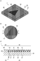
- FIG. 1A is a perspective view schematically showing an example of the shield package of the present invention.
- FIG. 1B is an enlarged view of a portion surrounded by a broken line in FIG.
- FIG. 1C is a sectional view taken along the line AA of FIG.
- FIG. 2A is a perspective view schematically showing an example of the shield package of the comparative technique in which one figure portion is drawn by one recess in the shield layer.
- FIG. 2B is an enlarged view of a portion surrounded by a broken line in FIG.
- FIG. 2C is a sectional view taken along the line BB of FIG.
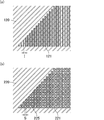
- FIGS. 3A and 3B are top views schematically showing an example of the shape of the groove formed in the sealing material of the shield package of the present invention.
- FIG. 3A and 3B are top views schematically showing an example of the shape of the groove formed in the sealing material of the shield package of the present invention.
- FIG. 4 is a process diagram schematically showing an example of a package preparation process in the shield package manufacturing method of the present invention.
- FIG. 5 is a process diagram schematically showing an example of the delineation-scheduled region determining process in the method for manufacturing a shield package of the present invention.
- FIG. 6 is an enlarged view of a portion surrounded by a broken line in FIG. 5, and is a process chart schematically showing an example of a drawing region forming process in the method for manufacturing a shield package of the present invention.
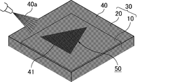
- FIG. 7 is a process chart schematically showing an example of a shield layer forming process in the method for manufacturing a shield package of the present invention.
- FIG. 8A is a photograph of the shield package according to the first embodiment.
- FIG. 8B is an enlarged photograph of the graphic portion of the shield package shown in FIG.
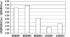
- FIG. 9 is a graph showing the ratio of (Sal of non-graphic portion) / (Sal of non-graphic portion) / (Sal of non-graphic portion) of the non-graphic portion of each shield package in each of the examples and the comparative examples.
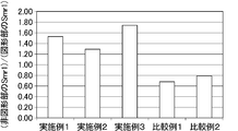
- FIG. 10 is a graph showing a ratio ((Smr1 of non-graphic part) / (Smr1 of graphic part)) of Smr1 of the non-graphic part and Smr1 of the graphic part of each shield package and each comparative example.
- FIG. 9 is a graph showing the ratio of (Sal of non-graphic portion) / (Sal of non-graphic portion) / (Sal of non-graphic portion) of the non-graphic portion of each shield package in each of the examples and the comparative examples.
- FIG. 10 is a graph showing a ratio ((Smr1 of non-graphic part) / (Smr1 of graphic part)
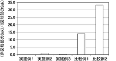
- FIG. 11 is a graph showing a ratio ((Ssk of non-graphic portion) / (Ssk of graphic portion)) of Ssk of non-graphic portion and Ssk of graphic portion of each shield package and each comparative example.
- FIG. 12 is a graph showing the ratio ((Rvk of non-graphic portion) / (Rvk of graphic portion)) of Rvk of the non-graphic portion and Rvk of the graphic portion of each shield package and each comparative example.
- FIG. 1A is a perspective view schematically showing an example of the shield package of the present invention.
- FIG. 1B is an enlarged view of a portion surrounded by a broken line in FIG.
- FIG. 1C is a sectional view taken along the line AA of FIG.
- the shield package 1 includes a package 30 in which the electronic component 10 is sealed with a sealing material 20, and a shield layer 40 that covers the package 30.
- the shield layer 40 has a graphic portion 50 and a non-graphic portion 60.
- the graphic portion 50 is drawn by gathering the concave portions 41 formed on the surface of the shield layer 40.
- the surface of the encapsulant 20 is composed of a drawing area 22 drawn linearly by gathering a plurality of groove portions 21 and a non-drawing area 23 other than the drawing area 22. Due to the groove 21, the plurality of recesses 41 are formed on the surface of the shield layer 40 located above the drawing region 22.
- FIG. 2A is a perspective view schematically showing an example of the shield package of the comparative technique in which one figure portion is drawn by one recess in the shield layer.
- FIG. 2B is an enlarged view of a portion surrounded by a broken line in FIG.
- FIG. 2C is a sectional view taken along the line BB of FIG.
- the shield package 501 includes a package 530 in which an electronic component 510 is sealed with a sealing material 520, and a shield layer 540 that covers the package 530.
- the graphic portion 550 is formed on the shield layer 540.
- the graphic portion 550 is formed by one recess 541 formed on the surface of the shield layer 540.
- a groove 521 is formed in the sealing material 520, and a drawing area 522 is formed in one groove 521.
- the other portion is the non-drawing area 523.
- This one groove portion 521 is formed by laser etching. By this etching, the bottom of one groove 521 is formed with fine irregularities 525 by laser etching.
- one recess 541 is formed on the surface of the shield layer 540 located above the drawing region 522 due to the groove 521.
- the conductive coating material is applied to form the shield layer 540.
- the shield layer 540 formed on the fine irregularities 525 becomes smooth due to the leveling effect of the conductive paint.
- it becomes difficult to distinguish the boundary of the concave portion 541 and the boundary of the graphic portion 550 becomes ambiguous.
- the graphic portion 50 is drawn on the surface of the shield layer 40 by gathering the plurality of recesses 41.
- the graphic portion 50 drawn in this way has a large difference in brightness from the non-graphic portion 60 due to the difference in reflectance. Therefore, the boundary of the graphic part 50 becomes clear.
- the ratio of Sal of the non-graphic part 60 to Sal of the graphic part 50 is (Sal of the non-graphic part) / (Sal of the graphic part)> 4.0.
- the ratio of Sal is in the above range, it is considered that the figure portion has more sharp irregularities than the non-figure portion, so that the reflection of light can be suppressed. Therefore, the difference in brightness between the graphic portion and the non-graphic portion becomes clear, and the distinctiveness of the graphic portion is further improved.
- these parameters can be controlled by adjusting the width and depth of the groove 21, the spacing between the grooves 21, the composition of the conductive coating material for forming the shield layer, and the like.
- the width W of the groove 21 (the distance indicated by the symbol “W” in FIG. 1C) is preferably 5 to 100 ⁇ m.
- the width W of the groove portion 21 is in the above range, the difference in lightness between the graphic portion 50 and the non-graphic portion 60 drawn on the surface of the shield layer 40 becomes clear.
- the width W of the groove 21 is less than 5 ⁇ m, the recess 41 is less likely to be formed on the surface of the shield layer 40.
- the difference in brightness between the graphic portion 50 and the non-graphic portion 60 on the surface of the shield layer 40 becomes small, and the graphic portion 50 becomes difficult to be identified.
- the leveling effect of the conductive paint makes it difficult for the graphic portion to be recognized by optical means such as a reader.
- the width W of the groove 21 exceeds 100 ⁇ m, the width of the recesses 41 formed on the surface of the shield layer 40 increases, so that the number of recesses 41 per unit area decreases. Therefore, the number of concave portions 41 for drawing the graphic portion 50 is reduced. As a result, the difference in lightness between the graphic portion 50 on the surface of the shield layer 40 and the non-graphic portion is small, and the graphic portion 50 is difficult to identify.
- the depth D of the groove 21 (the distance indicated by the symbol “D” in FIG. 1C) is preferably 5 ⁇ m or more, and more preferably 20 ⁇ m or more.
- the concave portion 41 is clearly formed on the surface of the shield layer 40, so that the figure portion 50 and the non-figure portion 60 that are drawn on the surface of the shield layer 40 are formed. The difference in brightness becomes clear.
- the groove may be formed in any shape as long as it can form a recess on the surface of the shield layer.
- the groove may have a linear shape or a dot shape.
- the groove is linear, it is easy to form by laser marking.
- FIGS. 3A and 3B are top views schematically showing an example of the shape of the groove formed in the sealing material of the shield package of the present invention.
- the groove portions 121 are formed linearly and in parallel with each other. Further, the intervals I between the adjacent groove portions 121 (the distance indicated by the symbol “I” in FIG. 3A) are equal intervals.
- the straight and parallel groove portions 121 can be efficiently formed because they have a simple shape.
- the interval I between the adjacent groove portions 121 is preferably 10 to 100 ⁇ m.
- the interval I between the groove portions 121 is in the above range, the difference between the graphic portion and the non-graphic portion drawn on the surface of the shield layer becomes clear. If the interval between the adjacent groove portions is less than 10 ⁇ m, many groove portions will be formed, so that it takes time to form the groove portions and it is not efficient. In addition, the leveling effect of the conductive paint makes it difficult for the graphic portion to be recognized by optical means such as a reader. If the distance between the adjacent groove portions exceeds 100 ⁇ m, the distance between the concave portions formed on the surface of the shield layer becomes wider, and the number of concave portions per unit area decreases. Therefore, the number of concave portions for drawing the graphic portion is reduced. As a result, the difference in lightness between the graphic portion and the non-graphic portion on the surface of the shield layer becomes small, making it difficult to identify the graphic portion.
- the intervals I between the adjacent groove portions 121 are equal, but in the shield package of the present invention, the intervals between the adjacent groove portions may not be equal.
- Grooves 221 are formed in a grid pattern in the sealing material 220 shown in FIG.
- the lattices formed by the groove portions 221 have the same shape.
- the lattice-shaped groove portions 221 can be easily formed by laser marking in a cross shape.
- the width S of the grating 225 formed by the groove portion 221 (the distance indicated by the symbol “S” in FIG. 3B) be 10 to 100 ⁇ m.
- the width S of the lattice 225 is in the above range, the difference in lightness between the graphic portion and the non-graphic portion drawn on the surface of the shield layer becomes clear. If the width of the grid formed by the groove portions is less than 10 ⁇ m, many groove portions will be formed, and it will take time to form the groove portions, which is not efficient.
- the leveling effect of the conductive paint makes it difficult for the graphic portion to be recognized by optical means such as a reader.
- the width of the lattice formed by the groove portions exceeds 100 ⁇ m, the interval between the recesses formed on the surface of the shield layer becomes wider, and the number of recesses per unit area decreases. Therefore, the number of concave portions for drawing the graphic portion is reduced. As a result, the difference in lightness between the graphic portion and the non-graphic portion on the surface of the shield layer becomes small, making it difficult to identify the graphic portion.
- the lattice formed by the groove 221 is a square having the same shape, but in the shield package of the present invention, the lattice formed by the groove does not have to be the same shape, and may be rectangular. Good.
- the electronic component is not particularly limited, and may be, for example, a conventional electronic component for wireless communication.
- the material of the sealing material that seals the electronic component is not particularly limited, and may be a resin material that is normally used.
- resin materials include epoxy resins, phenol resins, silicone resins, unsaturated polyester resins, melamine resins, urea resins, diallyl phthalate resins, polyimide resins, polyphenylene sulfide resins, and the like.
- the resin material may be composed of at least one selected from thermosetting resins, thermoplastic resins, and active energy ray-curable resins, but from the viewpoint of heat resistance, thermosetting resins or active It is desirable to be composed of an energy ray curable resin.
- the shield layer is not limited and may be formed of a known conductive paint.
- the shield layer may be made of a resin as a binder component and conductive particles.
- binder component forming the shield layer examples include epoxy resin, alkyd resin, melamine resin, xylene resin, and (meth) acrylate compound.
- the epoxy resin examples include bisphenol A type epoxy resin, bisphenol F type epoxy resin, bisphenol S type epoxy resin and other bisphenol type epoxy resin, spiro ring type epoxy resin, naphthalene type epoxy resin, biphenyl type epoxy resin, terpene type epoxy resin, Glycidyl ether type epoxy resins such as tris (glycidyloxyphenyl) methane and tetrakis (glycidyloxyphenyl) ethane, glycidyl amine type epoxy resins such as tetraglycidyl diaminodiphenylmethane, tetrabromobisphenol A type epoxy resin, cresol novolac type epoxy resin, phenol Examples thereof include novolac type epoxy resins, ⁇ -naphthol novolac type epoxy resins, novolac type epoxy resins such as brominated phenol novolac type epoxy resins, and rubber-modified epoxy resins.
- the (meth) acrylate compound is an acrylate compound or a methacrylate compound, and is not particularly limited as long as it is a compound having an acryloyl group or a methacryloyl group.
- Examples of (meth) acrylate compounds are isoamyl acrylate, neopentyl glycol diacrylate, trimethylolpropane triacrylate, ditrimethylolpropane tetraacrylate, 2-hydroxy-3-acryloyloxypropyl methacrylate, phenylglycidyl ether acrylate hexamethylene diisocyanate.
- examples thereof include urethane prepolymers, bisphenol A diglycidyl ether acrylic acid adducts, ethylene glycol dimethacrylate, and diethylene glycol dimethacrylate.
- Examples of the conductive particles forming the shield layer include metal particles such as copper particles, silver particles, nickel particles, silver-coated copper particles, gold-coated copper particles, silver-coated nickel particles, and gold-coated nickel particles.
- the shape of the metal particles is not particularly limited, and may be spherical, flaky (scaly), dendritic, fibrous, or the like.
- the spherical shape includes not only a substantially spherical shape (atomized powder) but also a substantially spherical shape such as a substantially polyhedral spherical shape (reducing powder) and an irregular shape (electrolytic powder).
- the shield layer is formed by curing a conductive coating material containing a curing agent
- the shield layer may contain a component derived from the curing agent.
- the shield layer may contain known additives such as a defoaming agent, a thickener, a pressure-sensitive adhesive, a filler, a flame retardant, and a colorant, if necessary.
- the graphic part on the surface of the shield layer may be a simple graphic, a character, a sign, or the like that indicates information having identifying power.
- the graphic portion When the graphic portion is a character, it may be a product model number, a lot number, a manufacturing date and time, or the like. When the graphic portion is a character, it is desirable that it can be visually recognized.
- a two-dimensional code can be given as an example of information that has discriminating power.
- the figure portion is a two-dimensional code, it is desirable that it can be read by a reader (for example, Honeywell's bar code scanner Xenon 1902 series).
- the surface of the sealing material 20 is formed in the plurality of groove portions 21 to form the graphic portion 50 on the surface of the shield layer 40.
- the ratio of the sal of the non-graphic portion to the sal of the graphic portion may be (Sal of the non-graphic portion) / (Sal of the graphic portion)> 4.0.
- the groove may not be formed on the surface of the.
- the graphic portion may be formed by forming a plurality of convex portions and / or a plurality of concave portions on the surface of the shield layer.
- the plurality of convex portions or the plurality of concave portions may be randomly arranged or may be regularly arranged.
- the plurality of convex portions or the plurality of concave portions may be drawn and / or dotted.
- the method for forming a plurality of protrusions and / or recesses on the surface of the shield layer is not particularly limited, and a method of processing the surface of the shield layer by embossing, sandblasting, or the like, or a conductive coating material for forming the shield layer A conventional method such as a method of adding particles to the can be used.
- a plurality of protrusions and / or recesses may be formed on the surface of the shield layer by applying a conductive paint to form the shield layer.
- a method of manufacturing a shield package according to the present invention includes (1) package preparation step, (2) drawing demarcation area determining step, (3) drawing area forming step, and (4) shield layer forming step. Each step will be described below with reference to the drawings.
- FIG. 4 is a process diagram schematically showing an example of a package preparation process in the shield package manufacturing method of the present invention.
- FIG. 5 is a process diagram schematically showing an example of the delineation-scheduled region determining process in the method for manufacturing a shield package of the present invention.
- FIG. 6 is an enlarged view of a portion surrounded by a broken line in FIG.
- FIG. 5 is a process chart schematically showing an example of a drawing region forming process in the method for manufacturing a shield package of the present invention.
- FIG. 7 is a process chart schematically showing an example of a shield layer forming process in the method for manufacturing a shield package of the present invention.
- FIG. 6 a plurality of linear groove portions 21 are formed by irradiating the drawing area 22a with a laser L, and the linear groove portions 21 are assembled.
- the drawing area 22 is drawn.
- the drawing area 22 is drawn by the linear groove portions 21 in FIG. 6, the drawing area may be drawn by forming dot-shaped groove portions in the method for manufacturing a shield package of the present invention.
- the width and depth of the groove formed in the drawing-destined area can be controlled by adjusting the laser output and moving speed. Further, at this time, in the shield layer formed through the subsequent steps, the ratio of Sal of the non-graphic portion to Sal of the graphic portion is (Sal of the non-graphic portion) / (Sal of the graphic portion)> 4.0. Therefore, the width and depth of the groove portions, the width between the groove portions, the composition of the conductive coating material applied to the package surface, and the like are controlled.
- the conductive coating material 40a is applied to the surface of the sealing material 20, the conductive coating material is cured to form the shield layer 40.
- the linear concave portion 41 caused by the linear groove portion 21 is formed, and the concave portions 41 are assembled to draw the graphic portion 50.
- the linear concave portion 41 is formed due to the linear groove portion 21.
- the dot-shaped groove may be formed in the drawing region forming step. In this case, a dot-shaped recess is formed, and the figure portion is stippled by the dot-shaped recess.
- the method for applying the conductive coating material is not particularly limited, and examples thereof include a spray method, a screen printing method, and a dipping method. Among these, it is desirable to apply by a spray method that can easily obtain a shield layer having a uniform thickness. Further, the thickness of the shield layer can be adjusted by controlling the spraying time and the like and adjusting the coating amount of the conductive paint.
- the conductive paint used in this step will be described.
- the conductive paint contains a binder component, conductive particles and a curing agent.
- the desirable types of the binder component and the conductive particles are the same as the desirable types of the binder component and the conductive particles forming the shield layer, and thus the description thereof is omitted here.
- the content of the conductive particles is preferably 500 to 1800 parts by weight, more preferably 550 to 1800 parts by weight, based on 100 parts by weight of the binder component.
- the curing agent examples include a phenol-based curing agent, an imidazole-based curing agent, an amine-based curing agent, a cationic-based curing agent, and a radical-based curing agent.
- phenol-based curing agent examples include novolac phenol and naphthol-based compounds.
- imidazole-based curing agent examples include imidazole, 2-undecylimidazole, 2-heptadecylimidazole, 2-methylimidazole, 2-ethylimidazole, 2-phenylimidazole, 2-ethyl-4-methyl-imidazole, 1-cyanoethyl. Examples include 2-undecylimidazole and 2-phenylimidazole.
- cationic curing agents are amine salts of boron trifluoride, P-methoxybenzenediazonium hexafluorophosphate, diphenyliodonium hexafluorophosphate, triphenylsulfonium, tetra-n-butylphosphonium tetraphenylborate, tetra- Onium compounds represented by n-butylphosphonium-o, o-diethylphosphorodithioate and the like can be mentioned.
- radical type curing agent examples include di-cumyl peroxide, t-butyl cumyl peroxide, t-butyl hydroperoxide, cumene hydroperoxide and the like.
- the amount of the curing agent mixed varies depending on the type of the curing agent, but normally, it is preferably 0.3 to 40 parts by weight, and 0.5 to 35 parts by weight based on 100 parts by weight of the total amount of the binder components. Is more desirable.
- the conductive paint may contain a solvent such as methyl ethyl ketone, if necessary.
- the viscosity of the conductive paint is preferably 10 to 5000 mPa ⁇ s. When the viscosity of the conductive paint is less than 10 mPa ⁇ s, the viscosity is too low and the irregularities are likely to be filled. When the viscosity of the conductive paint exceeds 5000 mPa ⁇ s, the viscosity becomes too high and the surface roughness of the coating film becomes large. As a result, the shield characteristics tend to deteriorate, and the appearance tends to deteriorate.
- a known curing method such as a method of curing the binder component by heating or a method of irradiating an activation energy ray to cure the binder component can be adopted.
- the curing conditions can be appropriately set according to the type and blending amount of the curing agent in the binder component.
- the ratio of the sal of the non-graphic portion to the sal of the graphic portion of the shield package according to the first embodiment is (Sal of the non-graphic portion) / (Sal of the graphic portion). )> 4.0, but the ratio of Smr1 of the non-graphic part to Smr1 of the graphic part is (Smr1 of the non-graphic part) / (Smr1 of the graphic part)> 1.0 2 is a shield package similar to the shield package according to the first embodiment of FIG.
- the Smr1 of the non-figure part and the graphic part can be measured by a confocal microscope (Latertec, OPTELICS HYBRID) according to ISO25178.
- the ratio of the sal of the non-graphic portion to the sal of the graphic portion of the shield package according to the first embodiment is (Sal of the non-graphic portion) / (Sal of the graphic portion). )> 4.0, but the ratio of Ssk of the non-graphic part to Ssk of the graphic part is (Ssk of non-graphic part) / (Ssk of graphic part) ⁇ 5.0.
- 2 is a shield package similar to the shield package according to the first embodiment of FIG.
- the figure portion has more fine convex portions than the non-figure portion, so that it is considered that the reflection of light is suppressed. Therefore, the difference in brightness between the graphic portion and the non-graphic portion becomes clear, and the distinctiveness of the graphic portion is further improved.
- the Ssks of the non-figure part and the graphic part can be measured by a confocal microscope (OPTELICS HYBRID manufactured by Lasertec Inc.) according to ISO25178.
- the ratio of the sal of the non-graphic portion to the sal of the graphic portion of the shield package according to the first embodiment is (Sal of the non-graphic portion) / (Sal of the graphic portion). )> 4.0, instead of the ratio Rvk of the non-graphic portion to the Rvk of the graphic portion being (Rvk of the non-graphic portion) / (Rvk of the graphic portion) ⁇ 0.4.
- 2 is a shield package similar to the shield package according to the first embodiment of FIG.
- the valleys on the surface of the graphic portion become sufficiently deeper than the valleys on the surface of the non-graphic portion, so that it is considered that the reflection of light is suppressed. Therefore, the difference in brightness between the graphic portion and the non-graphic portion becomes clear, and the distinctiveness of the graphic portion is further improved.
- the non-graphic part and Rvk can be measured by a confocal microscope (OPTELICS HYBRID manufactured by Lasertec) in accordance with JIS B 0601: 2001.
- the ratio of the sal of the non-graphic part to the sal of the graphic part is (Sal of the non-graphic part) / (Sal of the graphic part)> 4.0 ""
- the ratio of Smr1 of the non-graphic part to Smr1 of the graphic part is (Smr1 of the non-graphic part) / (Smr1 of the graphic part)> 1.0 ""
- non-figure The ratio of the part Ssk to the figure part Ssk is (non-figure part Ssk) / (figure part Ssk) ⁇ 5.0 ”and“ ratio of non-figure part Rvk and figure part Rvk Is (Rvk of non-figure part) / (Rvk of graphic part) ⁇ 0.4 ”.
- the ratio of Sal of the non-graphic portion to Sal of the graphic portion is (Sal of the non-graphic portion) / (Sal of the graphic portion)> 4.0”, “of the non-graphic portion”
- Sal, Smr1, and Ssk are parameters expressing a three-dimensional shape, and therefore the shield package of the present invention may satisfy these at the same time.
- Example 1 (1) Package Preparation Step A model package having a size of 1 cm in length and 1 cm in width is prepared by sealing the model IC with a sealing material made of a thermosetting epoxy resin.
- Planned drawing area determination process A drawing planned area that becomes a two-dimensional code and a non-drawing area other than that are determined on the surface of the encapsulating material of the model package.
- a conductive paint having the following composition was prepared.
- ⁇ Composition of conductive paint> ⁇ Binder component (epoxy resin) Mitsubishi Chemical Co., Ltd., product name "JER157S70” 20 parts by weight ADEKA Co., Ltd. product name "EP-3905S” 30 parts by weight ADEKA Co., Ltd.
- EP-4400 50 parts by mass -Conductive particles 1000 parts by weight of silver-coated copper alloy particles (average particle size 5 ⁇ m, flakes, aspect ratio 2-10) -Curing agent Phenol novolac (Arakawa Chemical Industry Co., Ltd., trade name “Tamanor 758") 15 parts by weight 2-methylimidazole (manufactured by Shikoku Chemicals Co., Ltd., trade name "2MZ-H”) 5 parts by weight Solvent 1-methoxy-2-propanol 24 Wt%
- spray coating was performed under the following conditions to form a shield layer having a thickness of 7 ⁇ m on the surface of the encapsulating material of the model package.
- a model shield package according to Example 1 was manufactured in which a plurality of recesses due to the groove were formed in the shield layer, and the two-dimensional code was drawn by assembling the recesses.
- FIG. 8A is a photograph of the shield package according to the first embodiment.
- FIG. 8B is an enlarged photograph of the graphic portion of the shield package shown in FIG.
- Examples 2 to 3 and Comparative Examples 1 to 2 In the (3) drawing area forming step, the shield packages according to Examples 2 to 3 and Comparative Examples 1 and 2 are the same as Example 1 except that the interval between the adjacent groove portions is changed as shown in Table 1. Was manufactured.
- FIG. 8 to 11 show the ratios of the parameters of the graphic part and the non-graphic part of the shield layer of the shield package in each of the examples and the comparative examples.
- FIG. 9 is a graph showing the ratio of (Sal of non-graphic portion) / (Sal of non-graphic portion) / (Sal of non-graphic portion) of the non-graphic portion of each shield package in each of the examples and the comparative examples.
- FIG. 10 is a graph showing a ratio ((Smr1 of non-graphic part) / (Smr1 of graphic part)) of Smr1 of the non-graphic part and Smr1 of the graphic part of each shield package and each comparative example.
- FIG. 9 is a graph showing the ratio of (Sal of non-graphic portion) / (Sal of non-graphic portion) / (Sal of non-graphic portion) of the non-graphic portion of each shield package in each of the examples and the comparative examples.
- FIG. 10 is a graph showing a ratio ((S
- FIG. 11 is a graph showing a ratio ((Ssk of non-graphic portion) / (Ssk of graphic portion)) of Ssk of non-graphic portion and Ssk of graphic portion of each shield package and each comparative example.
- FIG. 12 is a graph showing the ratio ((Rvk of non-graphic portion) / (Rvk of graphic portion)) of Rvk of the non-graphic portion and Rvk of the graphic portion of each shield package and each comparative example.
- the graphic portion could be read.
- the graphic portion could not be read.
- Shield package 10 1, 101, 201, 501 Shield package 10, 110, 210, 510 Electronic components 20, 120, 220, 520 Sealing material 21, 121, 221, 521 Groove 22, 522 Drawing area 22a Drawing scheduled area 23, 523 Region 30, 530 Package 40, 540 Shield layer 40a Conductive paint 41, 541 Recessed portion 50, 550 Graphic portion 60 Non-graphic portion 225 Lattice 525 Fine unevenness
Landscapes
- Engineering & Computer Science (AREA)
- Microelectronics & Electronic Packaging (AREA)
- Physics & Mathematics (AREA)
- Electromagnetism (AREA)
- General Physics & Mathematics (AREA)
- Theoretical Computer Science (AREA)
- Shielding Devices Or Components To Electric Or Magnetic Fields (AREA)
- Structures Or Materials For Encapsulating Or Coating Semiconductor Devices Or Solid State Devices (AREA)
- Health & Medical Sciences (AREA)
- Toxicology (AREA)
- Power Engineering (AREA)
Abstract
識別性が高い図形部がシールド層の表面に形成されたシールドパッケージを提供することを目的とする。 本発明のシールドパッケージは、電子部品が封止材により封止されたパッケージと、上記パッケージを覆うシールド層とからなるシールドパッケージであって、上記シールド層の表面には、図形部と上記図形部以外の非図形部とがあり、上記非図形部のSal(最小自己相関長さ)と上記図形部のSalとの比が、(非図形部のSal)/(図形部のSal)>4.0であることを特徴とする。
Description
本発明は、シールドパッケージに関する。
携帯電話やタブレット端末等の電子機器においては、近年、大容量のデータを伝送するための無線通信用の電子部品が封止材により封止されたパッケージとして多数実装されている。
このような無線通信用の電子部品は、ノイズを発生しやすいだけでなくノイズに対する感受性が高く、外部からのノイズに曝されると誤動作を起こしやすいという問題がある。
このような無線通信用の電子部品は、ノイズを発生しやすいだけでなくノイズに対する感受性が高く、外部からのノイズに曝されると誤動作を起こしやすいという問題がある。
また、電子機器の小型軽量化と高機能化を両立させるため、電子部品の実装密度を高めることが求められている。しかしながら、実装密度を高めるとノイズの発生源となる電子部品が増えるだけでなく、ノイズの影響を受ける電子部品も増えてしまうという問題がある。
従来から、ノイズの発生源である電子部品をパッケージごとシールド層で覆うことで、電子部品からのノイズの発生を防止するとともにノイズの侵入を防止した、いわゆるシールドパッケージが知られている(特許文献1、2)。
従来から、ノイズの発生源である電子部品をパッケージごとシールド層で覆うことで、電子部品からのノイズの発生を防止するとともにノイズの侵入を防止した、いわゆるシールドパッケージが知られている(特許文献1、2)。
また、電子部品が封止材により封止されたパッケージの識別性を向上させるために、パッケージの表面にレーザーマーキングをする方法も従来から行われている(特許文献3)。
シールドパッケージの識別性を向上させる方法としては、例えば、以下の方法がある。
まず、パッケージの封止材にレーザーを照射して封止材表面をエッチングすることにより溝部を形成する。このレーザーによるエッチングにより、封止材表面の溝部の底部には微細な凹凸が形成されることになる。
次に、スパッタリング法により、封止材に金属薄膜を堆積してシールド層を形成し、封止材表面の微細な凹凸に起因した凹凸を有するシールド層を形成することにより識別機能を有する図形部を形成するという方法がある。
まず、パッケージの封止材にレーザーを照射して封止材表面をエッチングすることにより溝部を形成する。このレーザーによるエッチングにより、封止材表面の溝部の底部には微細な凹凸が形成されることになる。
次に、スパッタリング法により、封止材に金属薄膜を堆積してシールド層を形成し、封止材表面の微細な凹凸に起因した凹凸を有するシールド層を形成することにより識別機能を有する図形部を形成するという方法がある。
スパッタリング法によって形成されたシールド層は、封止材表面の微細な凹凸に起因した凹凸を有し、その凹凸が図形部を形成するので、図形部の境界が判別しやすいという特徴がある。しかし、スパッタリング法によって形成されたシールド層は、電子部品を封止している封止材と金属薄膜との線膨張率が異なるので、ヒートサイクル試験における信頼性が悪いという問題点があった。さらに、スパッタリング装置は高価であるため生産性が充分といえなかった。
また、スプレー法により導電性塗料を封止材の表面に塗布すると、導電性塗料のレベリング効果によって、封止材の溝部の微細な凹凸の上に形成されるシールド層は、なだらかになる。その結果、レーザーを照射した箇所の境界が判別しにくくなり、識別機能を有する図形部の境界が曖昧になるという問題が生じることがある。
本発明は、上記問題を解決するためになされたものであり、本発明の目的は、識別性が高い図形部がシールド層の表面に形成されたシールドパッケージを提供することである。
本発明のシールドパッケージでは、シールド層の表面には、図形部と上記図形部以外の非図形部とがある。
本発明のシールドパッケージでは、非図形部の形状を表現する特定のパラメータと図形部の形状を表現する当該特定のパラメータとの比が、所定の関係を満たすことにより、非図形部と図形部の反射率に差が生じ、図形部以外の非図形部との明度の差が大きくなる。そのため、図形部の境界が明確になる。従って、本発明のシールドパッケージでは、図形部の識別性が高い。
なお、本明細書において「図形部」とは、円や三角形等の単純図形に加え、文字や標識等の識別力を有する情報を示すものも含む。
また、「識別力を有する情報を示すもの」とは、目視により識別できるものに加え、リーダー等の光学的手段により識別できるものを含む。
本発明のシールドパッケージでは、非図形部の形状を表現する特定のパラメータと図形部の形状を表現する当該特定のパラメータとの比が、所定の関係を満たすことにより、非図形部と図形部の反射率に差が生じ、図形部以外の非図形部との明度の差が大きくなる。そのため、図形部の境界が明確になる。従って、本発明のシールドパッケージでは、図形部の識別性が高い。
なお、本明細書において「図形部」とは、円や三角形等の単純図形に加え、文字や標識等の識別力を有する情報を示すものも含む。
また、「識別力を有する情報を示すもの」とは、目視により識別できるものに加え、リーダー等の光学的手段により識別できるものを含む。
本発明のシールドパッケージは、電子部品が封止材により封止されたパッケージと、上記パッケージを覆うシールド層とからなるシールドパッケージであって、上記シールド層の表面には、図形部と上記図形部以外の非図形部とがあり、上記非図形部のSal(最小自己相関長さ)と上記図形部のSalとの比が、(非図形部のSal)/(図形部のSal)>4.0であることを特徴とする。
本発明のシールドパッケージでは、非図形部の形状を表現する特定のパラメータ、及び、図形部の形状を表現する当該特定のパラメータはSal(最小自己相関長さ)である。
Salの比が上記範囲であると、図形部の方が非図形部よりも急激な凹凸が多くなるため、光の反射が抑えられると考えられる。そのため、図形部と非図形部との間の明暗の差が明確になり、図形部の識別性がより向上する。
Salの比が上記範囲であると、図形部の方が非図形部よりも急激な凹凸が多くなるため、光の反射が抑えられると考えられる。そのため、図形部と非図形部との間の明暗の差が明確になり、図形部の識別性がより向上する。
本発明の別のシールドパッケージは、電子部品が封止材により封止されたパッケージと、前記パッケージを覆うシールド層とからなるシールドパッケージであって、前記シールド層の表面には、図形部と前記図形部以外の非図形部とがあり、上記非図形部のSmr1(突出山部とコア部を分離する負荷面積率)と上記図形部のSmr1との比が、(非図形部のSmr1)/(図形部のSmr1)>1.0であることを特徴とする。
本発明の別のシールドパッケージでは、非図形部の形状を表現する特定のパラメータ、及び、図形部の形状を表現する当該特定のパラメータはSmr1(突出山部とコア部を分離する負荷面積率)である。
Smr1の比が上記範囲であると、図形部の方が非図形部よりも急激な凹凸が多くなるため、光の反射が抑えられると考えられる。そのため、図形部と非図形部との間の明暗の差が明確になり、図形部の識別性がより向上する。
Smr1の比が上記範囲であると、図形部の方が非図形部よりも急激な凹凸が多くなるため、光の反射が抑えられると考えられる。そのため、図形部と非図形部との間の明暗の差が明確になり、図形部の識別性がより向上する。
本発明の別のシールドパッケージは、電子部品が封止材により封止されたパッケージと、前記パッケージを覆うシールド層とからなるシールドパッケージであって、前記シールド層の表面には、図形部と前記図形部以外の非図形部とがあり、上記非図形部のSsk(スキューネス)と上記図形部のSskとの比が、(非図形部のSsk)/(図形部のSsk)<5.0であることを特徴とする。
本発明の別のシールドパッケージでは、非図形部の形状を表現する特定のパラメータ、及び、図形部の形状を表現する当該特定のパラメータはSsk(スキューネス)である。
Sskの比が上記範囲であると、図形部の方が非図形部よりも細かな凸部が多くなるので、光の反射が抑えられると考えられる。そのため、図形部と非図形部との間の明暗の差が明確になり、図形部の識別性がより向上する。
Sskの比が上記範囲であると、図形部の方が非図形部よりも細かな凸部が多くなるので、光の反射が抑えられると考えられる。そのため、図形部と非図形部との間の明暗の差が明確になり、図形部の識別性がより向上する。
本発明の別のシールドパッケージは、電子部品が封止材により封止されたパッケージと、上記パッケージを覆うシールド層とからなるシールドパッケージであって、上記シールド層の表面には、図形部と上記図形部以外の非図形部とがあり、上記非図形部のRvk(突出谷部深さ)と上記図形部のRvkとの比が、(非図形部のRvk)/(図形部のRvk)<0.4であることを特徴とする。
本発明の別のシールドパッケージでは、非図形部の形状を表現する特定のパラメータ、及び、図形部の形状を表現する当該特定のパラメータは、Rvk(突出谷部深さ)である。
Rvkの比が上記範囲であると、図形部の表面における谷部が非図形部の表面における谷部よりも充分に深くなるため、光の反射が抑えられると考えられる。そのため、図形部と非図形部との間の明暗の差が明確になり、図形部の識別性がより向上する。
Rvkの比が上記範囲であると、図形部の表面における谷部が非図形部の表面における谷部よりも充分に深くなるため、光の反射が抑えられると考えられる。そのため、図形部と非図形部との間の明暗の差が明確になり、図形部の識別性がより向上する。
本発明のシールドパッケージでは、上記封止材の表面は、複数の溝部が集合することにより線描及び/又は点描された描写領域と、上記描写領域以外の非描写領域とからなり、上記描写領域の上に位置する上記シールド層の表面には、上記溝部に起因する複数の凹部が形成されており、上記凹部は、集合して上記図形部を線描及び/又は点描していてもよい。
封止材の表面に溝部を形成することにより、容易にシールド層の表面に図形部を形成することができる。
また、線描及び/又は点描により図形部を形成するため、図形部の識別性は良好になる。
封止材の表面に溝部を形成することにより、容易にシールド層の表面に図形部を形成することができる。
また、線描及び/又は点描により図形部を形成するため、図形部の識別性は良好になる。
本発明のシールドパッケージでは、複数の上記溝部の内、少なくとも一部は、線状に形成されていてもよい。
線状の溝部はレーザーマーキングにより形成しやすい。
線状の溝部はレーザーマーキングにより形成しやすい。
本発明のシールドパッケージでは、複数の上記溝部の内、少なくとも一部は、直線状に、かつ、上記溝部同士が平行になるように形成されていることが望ましい。
直線状、かつ、平行な溝部は、単純な形状なので効率的に形成することができる。
直線状、かつ、平行な溝部は、単純な形状なので効率的に形成することができる。
本発明のシールドパッケージでは、隣り合う上記溝部同士の間隔は、10~100μmであることが望ましい。
溝部同士の間隔が上記範囲であると、シールド層の表面に線描される図形部と、非図形部との明度の差がより明確になる。
隣り合う溝部同士の間隔が、10μm未満であると、溝部形成に時間がかかり効率的でない。また、導電性塗料のレベリング効果により、リーダー等の光学的手段で図形部が認識されにくくなる。
隣り合う溝部同士の間隔が、100μmを超えると、シールド層の表面に形成される凹部の間隔が広がり、単位面積当たりの凹部の数が少なくなる。そのため、図形部を線描する凹部の数が少なくなる。
その結果、シールド層の表面の図形部と、非図形部との明度の差が小さくなり、図形部が識別されにくくなる。
溝部同士の間隔が上記範囲であると、シールド層の表面に線描される図形部と、非図形部との明度の差がより明確になる。
隣り合う溝部同士の間隔が、10μm未満であると、溝部形成に時間がかかり効率的でない。また、導電性塗料のレベリング効果により、リーダー等の光学的手段で図形部が認識されにくくなる。
隣り合う溝部同士の間隔が、100μmを超えると、シールド層の表面に形成される凹部の間隔が広がり、単位面積当たりの凹部の数が少なくなる。そのため、図形部を線描する凹部の数が少なくなる。
その結果、シールド層の表面の図形部と、非図形部との明度の差が小さくなり、図形部が識別されにくくなる。
本発明のシールドパッケージでは、複数の上記溝部の内、少なくとも一部は、格子状に形成されていてもよい。
格子状の溝部は、十字にレーザーマーキングすることにより容易に形成することができる。
格子状の溝部は、十字にレーザーマーキングすることにより容易に形成することができる。
本発明のシールドパッケージでは、上記溝部により形成される格子の幅は、10~100μmであることが望ましい。
溝部により形成される格子の幅が、上記範囲であると、シールド層の表面に線描される図形部と、非図形部との明度の差が明確になる。
溝部により形成される格子の幅が、10μm未満であると、溝部形成に時間がかかり効率的でない。また、導電性塗料のレベリング効果により、リーダー等の光学的手段で図形部が認識されにくくなる。
溝部により形成される格子の幅が、100μmを超えると、シールド層の表面に形成される凹部の間隔が広がり、単位面積当たりの凹部の数が少なくなる。そのため、図形部を線描する凹部の数が少なくなる。
その結果、シールド層の表面の図形部と、非図形部と明度の差が小さくなり、図形部が識別されにくくなる。
溝部により形成される格子の幅が、上記範囲であると、シールド層の表面に線描される図形部と、非図形部との明度の差が明確になる。
溝部により形成される格子の幅が、10μm未満であると、溝部形成に時間がかかり効率的でない。また、導電性塗料のレベリング効果により、リーダー等の光学的手段で図形部が認識されにくくなる。
溝部により形成される格子の幅が、100μmを超えると、シールド層の表面に形成される凹部の間隔が広がり、単位面積当たりの凹部の数が少なくなる。そのため、図形部を線描する凹部の数が少なくなる。
その結果、シールド層の表面の図形部と、非図形部と明度の差が小さくなり、図形部が識別されにくくなる。
本発明のシールドパッケージでは、上記溝部の幅は、5~100μmであることが望ましい。
溝部の幅が、上記範囲であると、シールド層の表面に線描及び/又は点描される図形部と、非図形部との明度の差が明確になる。
溝部の幅が、5μm未満であると、シールド層の表面に凹部が形成されにくくなる。その結果、シールド層の表面の図形部と、非図形部との明度の差が小さくなり、図形部が識別されにくくなる。また、導電性塗料のレベリング効果により、リーダー等の光学的手段で図形部が認識されにくくなる。
溝部の幅が、100μmを超えると、シールド層の表面に形成される凹部の幅が広がるので、単位面積当たりの凹部の数が少なくなる。そのため、図形部を線描する凹部の数が少なくなる。
その結果、シールド層の表面の図形部と、非図形部との明度の差が小さくなり、図形部が識別されにくくなる。
溝部の幅が、上記範囲であると、シールド層の表面に線描及び/又は点描される図形部と、非図形部との明度の差が明確になる。
溝部の幅が、5μm未満であると、シールド層の表面に凹部が形成されにくくなる。その結果、シールド層の表面の図形部と、非図形部との明度の差が小さくなり、図形部が識別されにくくなる。また、導電性塗料のレベリング効果により、リーダー等の光学的手段で図形部が認識されにくくなる。
溝部の幅が、100μmを超えると、シールド層の表面に形成される凹部の幅が広がるので、単位面積当たりの凹部の数が少なくなる。そのため、図形部を線描する凹部の数が少なくなる。
その結果、シールド層の表面の図形部と、非図形部との明度の差が小さくなり、図形部が識別されにくくなる。
本発明のシールドパッケージでは、上記溝部の深さは、5μm以上であることが望ましい。
溝部の深さが、5μm以上であると、シールド層の表面にはっきりと凹部が形成されるので、シールド層の表面に線描及び/又は点描される図形部と、非図形部との明度の差が明確になる。
溝部の深さが、5μm以上であると、シールド層の表面にはっきりと凹部が形成されるので、シールド層の表面に線描及び/又は点描される図形部と、非図形部との明度の差が明確になる。
本発明のシールドパッケージでは、上記シールド層の厚さは、3~15μmであることが望ましい。
シールド層の厚さが3μm未満であると、充分なシールド性能を得られにくくなる。
シールド層の厚さが15μmを超えると、溝部からシールド層の表面までの距離が長くなるので、凹部が形成されにくくなる。
その結果、シールド層の表面の図形部と、非図形部との明度の差が小さくなり、図形部が識別されにくくなる。
シールド層の厚さが3μm未満であると、充分なシールド性能を得られにくくなる。
シールド層の厚さが15μmを超えると、溝部からシールド層の表面までの距離が長くなるので、凹部が形成されにくくなる。
その結果、シールド層の表面の図形部と、非図形部との明度の差が小さくなり、図形部が識別されにくくなる。
本発明のシールドパッケージでは、上記図形部は、二次元コードであることが望ましい。
上記の通り、本発明のシールドパッケージでは、図形部の識別性が高い。そのため、図形部が二次元コードであったとしてもリーダー等の光学的手段で容易に読み取ることができる。
上記の通り、本発明のシールドパッケージでは、図形部の識別性が高い。そのため、図形部が二次元コードであったとしてもリーダー等の光学的手段で容易に読み取ることができる。
本発明のシールドパッケージでは、非図形部のSalと図形部のSalとの比が、(非図形部のSal)/(図形部のSal)>4.0である。
Salの比が上記範囲であると、図形部の方が非図形部よりも急激な凹凸が多くなるため、光の反射が抑えられると考えられる。そのため、図形部と非図形部との間の明暗の差が明確になり、図形部の識別性がより向上する。
Salの比が上記範囲であると、図形部の方が非図形部よりも急激な凹凸が多くなるため、光の反射が抑えられると考えられる。そのため、図形部と非図形部との間の明暗の差が明確になり、図形部の識別性がより向上する。
本発明の別のシールドパッケージでは、非図形部のSmr1と図形部のSmr1との比が、(非図形部のSmr1)/(図形部のSmr1)>1.0である。
Smr1の比が上記範囲であると、図形部の方が非図形部よりも急激な凹凸が多くなるため、光の反射が抑えられると考えられる。そのため、図形部と非図形部との間の明暗の差が明確になり、図形部の識別性がより向上する。
Smr1の比が上記範囲であると、図形部の方が非図形部よりも急激な凹凸が多くなるため、光の反射が抑えられると考えられる。そのため、図形部と非図形部との間の明暗の差が明確になり、図形部の識別性がより向上する。
本発明の別のシールドパッケージでは、非図形部のSskと図形部のSskとの比が、(非図形部のSsk)/(図形部のSsk)<5.0である。
Sskの比が上記範囲であると、図形部の方が非図形部よりも細かな凸部が多くなるので、光の反射が抑えられると考えられる。そのため、図形部と非図形部との間の明暗の差が明確になり、図形部の識別性がより向上する。
Sskの比が上記範囲であると、図形部の方が非図形部よりも細かな凸部が多くなるので、光の反射が抑えられると考えられる。そのため、図形部と非図形部との間の明暗の差が明確になり、図形部の識別性がより向上する。
本発明のシールドパッケージでは、非図形部のRvkと図形部のRvkとの比が、(非図形部のRvk)/(図形部のRvk)<0.4である。
Rvkの比が上記範囲であると、図形部の表面における谷部が非図形部の表面における谷部よりも充分に深くなるため、光の反射が抑えられると考えられる。そのため、図形部と非図形部との間の明暗の差が明確になり、図形部の識別性がより向上する。
Rvkの比が上記範囲であると、図形部の表面における谷部が非図形部の表面における谷部よりも充分に深くなるため、光の反射が抑えられると考えられる。そのため、図形部と非図形部との間の明暗の差が明確になり、図形部の識別性がより向上する。
以下、本発明のシールドパッケージについて具体的に説明する。しかしながら、本発明は、以下の実施形態に限定されるものではなく、本発明の要旨を変更しない範囲において適宜変更して適用することができる。
(第1実施形態)
本発明のシールドパッケージの一態様について、以下に図面を用いて説明する。
図1(a)は、本発明のシールドパッケージの一例を模式的に示す斜視図である。図1(b)は、図1(a)中、破線で囲った部分の拡大図である。図1(c)は、図1(b)のA-A線断面図である。
本発明のシールドパッケージの一態様について、以下に図面を用いて説明する。
図1(a)は、本発明のシールドパッケージの一例を模式的に示す斜視図である。図1(b)は、図1(a)中、破線で囲った部分の拡大図である。図1(c)は、図1(b)のA-A線断面図である。
図1(a)に示すように、シールドパッケージ1は、電子部品10が封止材20により封止されたパッケージ30と、パッケージ30を覆うシールド層40とからなる。
そして、シールド層40には、図形部50と非図形部60とがある。
そして、シールド層40には、図形部50と非図形部60とがある。
図1(b)に示すように、図形部50は、シールド層40の表面に形成された凹部41が集合することにより線描されている。
また、図1(c)に示すように、封止材20の表面は、複数の溝部21が集合することにより線描された描写領域22と、描写領域22以外の非描写領域23とからなる。
複数の凹部41は、溝部21に起因して、描写領域22の上に位置するシールド層40の表面に形成されている。
複数の凹部41は、溝部21に起因して、描写領域22の上に位置するシールド層40の表面に形成されている。
ここで、一つの溝部により封止材に描写領域を形成し、その上にシールド層を形成して凹部を形成し、一つの凹部により一つの図形部を描く、比較技術のシールドパッケージについて説明する。
図2(a)は、シールド層において、一つの凹部により一つの図形部を描いた比較技術のシールドパッケージの一例を模式的に示す斜視図である。図2(b)は、図2(a)中、破線で囲った部分の拡大図である。図2(c)は、図2(b)のB-B線断面図である。
図2(a)は、シールド層において、一つの凹部により一つの図形部を描いた比較技術のシールドパッケージの一例を模式的に示す斜視図である。図2(b)は、図2(a)中、破線で囲った部分の拡大図である。図2(c)は、図2(b)のB-B線断面図である。
図2(a)に示すようにシールドパッケージ501は、電子部品510が封止材520により封止されたパッケージ530と、パッケージ530を覆うシールド層540とからなる。
そして、シールド層540には、図形部550が形成されている。
そして、シールド層540には、図形部550が形成されている。
図2(b)に示すように、図形部550は、シールド層540の表面に形成された一つの凹部541により形成されている。
また、図2(c)に示すように、封止材520には、溝部521が形成されており、一つの溝部521で描写領域522が形成されている。また、それ以外の部分は、非描写領域523である。
この一つの溝部521はレーザーによるエッチングにより形成されている。
このエッチングにより一つの溝部521の底部は、レーザーエッチングにより微細な凹凸525が形成されている。
この一つの溝部521はレーザーによるエッチングにより形成されている。
このエッチングにより一つの溝部521の底部は、レーザーエッチングにより微細な凹凸525が形成されている。
また、一つの凹部541が、溝部521に起因して、描写領域522の上に位置するシールド層540の表面に形成されている。
このようなシールドパッケージ501を製造する場合、封止材520に溝部521を形成した後、導電性塗料を塗布してシールド層540を形成することになる。
図2(c)の破線で囲った部分に示されるように、導電性塗料のレベリング効果によって、微細な凹凸525の上に形成されるシールド層540は、なだらかになる。その結果、凹部541の境界が判別しにくくなり、図形部550の境界が曖昧になる。
図2(c)の破線で囲った部分に示されるように、導電性塗料のレベリング効果によって、微細な凹凸525の上に形成されるシールド層540は、なだらかになる。その結果、凹部541の境界が判別しにくくなり、図形部550の境界が曖昧になる。
一方、シールドパッケージ1では、複数の凹部41が集合することにより、シールド層40の表面に図形部50が線描されている。
このように線描された図形部50は、反射率の違いにより、非図形部60との明度の差が大きくなる。そのため、図形部50の境界が明確になる。
このように線描された図形部50は、反射率の違いにより、非図形部60との明度の差が大きくなる。そのため、図形部50の境界が明確になる。
シールドパッケージ1では、非図形部60のSalと図形部50のSalとの比が、(非図形部のSal)/(図形部のSal)>4.0である。
Salの比が上記範囲であると、図形部の方が非図形部よりも急激な凹凸が多くなるため、光の反射が抑えられると考えられる。そのため、図形部と非図形部との間の明暗の差が明確になり、図形部の識別性がより向上する。
Salの比が上記範囲であると、図形部の方が非図形部よりも急激な凹凸が多くなるため、光の反射が抑えられると考えられる。そのため、図形部と非図形部との間の明暗の差が明確になり、図形部の識別性がより向上する。
なお、非図形部60及び図形部50のSalは、ISO25178に準拠して、コンフォーカル顕微鏡(Lasertec社製、OPTELICS HYBRID)により測定することができる。
また、これらのパラメータは、溝部21の幅、深さ、溝部21同士の間隔、シールド層を形成するための導電性塗料の組成等を調整することにより制御することができる。
シールドパッケージ1では、溝部21の幅W(図1(c)中、符号「W」で示す距離)は、5~100μmであることが望ましい。
溝部21の幅Wが、上記範囲であると、シールド層40の表面に線描される図形部50と、非図形部60との明度の差が明確になる。
溝部21の幅Wが、5μm未満であると、シールド層40の表面に凹部41が形成されにくくなる。その結果、シールド層40の表面の図形部50と、非図形部60との明度の差が小さくなり、図形部50が識別されにくくなる。また、導電性塗料のレベリング効果により、リーダー等の光学的手段で図形部が認識されにくくなる。
溝部21の幅Wが、100μmを超えると、シールド層40の表面に形成される凹部41の幅が広がるので、単位面積当たりの凹部41の数が少なくなる。そのため、図形部50を線描する凹部41の数が少なくなる。
その結果、シールド層40の表面の図形部50と、そうでない部分との明度の差が小さくなり、図形部50が識別されにくくなる。
溝部21の幅Wが、上記範囲であると、シールド層40の表面に線描される図形部50と、非図形部60との明度の差が明確になる。
溝部21の幅Wが、5μm未満であると、シールド層40の表面に凹部41が形成されにくくなる。その結果、シールド層40の表面の図形部50と、非図形部60との明度の差が小さくなり、図形部50が識別されにくくなる。また、導電性塗料のレベリング効果により、リーダー等の光学的手段で図形部が認識されにくくなる。
溝部21の幅Wが、100μmを超えると、シールド層40の表面に形成される凹部41の幅が広がるので、単位面積当たりの凹部41の数が少なくなる。そのため、図形部50を線描する凹部41の数が少なくなる。
その結果、シールド層40の表面の図形部50と、そうでない部分との明度の差が小さくなり、図形部50が識別されにくくなる。
シールドパッケージ1では、溝部21の深さD(図1(c)中、符号「D」で示す距離)は、5μm以上であることが望ましく、20μm以上であることがより望ましい。
溝部21の深さDが、5μm以上であると、シールド層40の表面にはっきりと凹部41が形成されるので、シールド層40の表面に線描される図形部50と、非図形部60との明度の差が明確になる。
溝部21の深さDが、5μm以上であると、シールド層40の表面にはっきりと凹部41が形成されるので、シールド層40の表面に線描される図形部50と、非図形部60との明度の差が明確になる。
本発明のシールドパッケージにおいて、溝部は、シールド層の表面に凹部が形成できる形状であれば、どのように形成されていてもよい。
例えば、溝部は、線状であってもよく、点状であってもよい。
特に、溝部が線状である場合、レーザーマーキングにより形成しやすい。
例えば、溝部は、線状であってもよく、点状であってもよい。
特に、溝部が線状である場合、レーザーマーキングにより形成しやすい。
ここで、本発明のシールドパッケージにおける溝部の形状について図面を用いて説明する。
図3(a)及び(b)は、本発明のシールドパッケージの封止材に形成した溝部の形状の一例を模式的に示す上面図である。
図3(a)及び(b)は、本発明のシールドパッケージの封止材に形成した溝部の形状の一例を模式的に示す上面図である。
図3(a)に示す封止材120には、溝部121が、直線状に、かつ、溝部121同士が平行になるように形成されている。
また、隣り合う溝部121同士の間隔I(図3(a)中、符号「I」で示す距離)は等間隔である。
直線状、かつ、平行な溝部121は、単純な形状なので効率的に形成することができる。
また、隣り合う溝部121同士の間隔I(図3(a)中、符号「I」で示す距離)は等間隔である。
直線状、かつ、平行な溝部121は、単純な形状なので効率的に形成することができる。
封止材120では、隣り合う溝部121同士の間隔Iは、10~100μmであることが望ましい。
溝部121同士の間隔Iが上記範囲であると、シールド層の表面に線描される図形部と、非図形部の差が明確になる。
隣り合う溝部同士の間隔が、10μm未満であると、多くの溝部を形成することになるので、溝部形成に時間がかかり効率的でない。また、導電性塗料のレベリング効果により、リーダー等の光学的手段で図形部が認識されにくくなる。
隣り合う溝部同士の間隔が、100μmを超えると、シールド層の表面に形成される凹部の間隔が広がり、単位面積当たりの凹部の数が少なくなる。そのため、図形部を線描する凹部の数が少なくなる。
その結果、シールド層の表面の図形部と、非図形部との明度の差が小さくなり、図形部が識別されにくくなる。
溝部121同士の間隔Iが上記範囲であると、シールド層の表面に線描される図形部と、非図形部の差が明確になる。
隣り合う溝部同士の間隔が、10μm未満であると、多くの溝部を形成することになるので、溝部形成に時間がかかり効率的でない。また、導電性塗料のレベリング効果により、リーダー等の光学的手段で図形部が認識されにくくなる。
隣り合う溝部同士の間隔が、100μmを超えると、シールド層の表面に形成される凹部の間隔が広がり、単位面積当たりの凹部の数が少なくなる。そのため、図形部を線描する凹部の数が少なくなる。
その結果、シールド層の表面の図形部と、非図形部との明度の差が小さくなり、図形部が識別されにくくなる。
図3(a)では、隣り合う溝部121同士の間隔Iは等間隔であるが、本発明のシールドパッケージでは、隣り合う溝部同士の間隔は等間隔でなくてもよい。
図3(b)に示す封止材220には、溝部221が格子状に形成されている。
また、溝部221により形成される格子は、それぞれが互いに同じ形状である。
格子状の溝部221は、十字にレーザーマーキングすることにより容易に形成することができる。
また、溝部221により形成される格子は、それぞれが互いに同じ形状である。
格子状の溝部221は、十字にレーザーマーキングすることにより容易に形成することができる。
封止材220では、溝部221により形成される格子225の幅S(図3(b)中、符号「S」で示す距離)は、10~100μmであることが望ましい。
格子225の幅Sが、上記範囲であると、シールド層の表面に線描される図形部と、非図形部との明度の差が明確になる。
溝部により形成される格子の幅が、10μm未満であると、多くの溝部を形成することになるので、溝部形成に時間がかかり効率的でない。また、導電性塗料のレベリング効果により、リーダー等の光学的手段で図形部が認識されにくくなる。
溝部により形成される格子の幅が、100μmを超えると、シールド層の表面に形成される凹部の間隔が広がり、単位面積当たりの凹部の数が少なくなる。そのため、図形部を線描する凹部の数が少なくなる。
その結果、シールド層の表面の図形部と、非図形部との明度の差が小さくなり、図形部が識別されにくくなる。
格子225の幅Sが、上記範囲であると、シールド層の表面に線描される図形部と、非図形部との明度の差が明確になる。
溝部により形成される格子の幅が、10μm未満であると、多くの溝部を形成することになるので、溝部形成に時間がかかり効率的でない。また、導電性塗料のレベリング効果により、リーダー等の光学的手段で図形部が認識されにくくなる。
溝部により形成される格子の幅が、100μmを超えると、シールド層の表面に形成される凹部の間隔が広がり、単位面積当たりの凹部の数が少なくなる。そのため、図形部を線描する凹部の数が少なくなる。
その結果、シールド層の表面の図形部と、非図形部との明度の差が小さくなり、図形部が識別されにくくなる。
図3(b)では、溝部221により形成される格子は同じ形状の正方形であるが、本発明のシールドパッケージでは、溝部により形成される格子は同じ形状でなくてもよく、長方形であってもよい。
本発明のシールドパッケージにおいて、電子部品は、特に限定されず、例えば、従来の無線通信用の電子部品であってもよい。
本発明のシールドパッケージにおいて、電子部品を封止する封止材の材料は、特に限定されず、通常使用される樹脂材料であってもよい。
このような樹脂材料としては、エポキシ樹脂、フェノール樹脂、シリコーン樹脂、不飽和ポリエステル樹脂、メラミン樹脂、ユリア樹脂、ジアリルフタレート樹脂、ポリイミド樹脂、ポリフェニレンサルフィド樹脂等が挙げられる。
また、樹脂材料は、熱硬化性樹脂や熱可塑性樹脂、活性エネルギー線硬化性樹脂から選択される少なくともいずれか一つにより構成されていても良いが、耐熱性の観点から熱硬化性樹脂又は活性エネルギー線硬化性樹脂により構成されることが望ましい。
このような樹脂材料としては、エポキシ樹脂、フェノール樹脂、シリコーン樹脂、不飽和ポリエステル樹脂、メラミン樹脂、ユリア樹脂、ジアリルフタレート樹脂、ポリイミド樹脂、ポリフェニレンサルフィド樹脂等が挙げられる。
また、樹脂材料は、熱硬化性樹脂や熱可塑性樹脂、活性エネルギー線硬化性樹脂から選択される少なくともいずれか一つにより構成されていても良いが、耐熱性の観点から熱硬化性樹脂又は活性エネルギー線硬化性樹脂により構成されることが望ましい。
本発明のシールドパッケージでは、シールド層は限定されず、公知の導電性塗料により形成されていてもよい。
シールド層は、バインダ成分である樹脂と、導電性粒子からなっていてもよい。
シールド層は、バインダ成分である樹脂と、導電性粒子からなっていてもよい。
シールド層を構成するバインダ成分としては、例えば、エポキシ樹脂、アルキド樹脂、メラミン樹脂、キシレン樹脂、(メタ)アクリレート化合物等が挙げられる。
エポキシ樹脂としては、ビスフェノールA型エポキシ樹脂、ビスフェノールF型エポキシ樹脂、ビスフェノールS型エポキシ樹脂などのビスフェノール型エポキシ樹脂、スピロ環型エポキシ樹脂、ナフタレン型エポキシ樹脂、ビフェニル型エポキシ樹脂、テルペン型エポキシ樹脂、トリス(グリシジルオキシフェニル)メタン、テトラキス(グリシジルオキシフェニル)エタンなどのグリシジルエーテル型エポキシ樹脂、テトラグリシジルジアミノジフェニルメタンなどのグリシジルアミン型エポキシ樹脂、テトラブロムビスフェノールA型エポキシ樹脂、クレゾールノボラック型エポキシ樹脂、フェノールノボラック型エポキシ樹脂、α-ナフトールノボラック型エポキシ樹脂、臭素化フェノールノボラック型エポキシ樹脂等のノボラック型エポキシ樹脂、ゴム変性エポキシ樹脂等が挙げられる。
(メタ)アクリレート化合物とは、アクリレート化合物又はメタクリレート化合物であり、アクリロイル基又はメタクリロイル基を有する化合物であれば特に限定されない。(メタ)アクリレート化合物の例としては、イソアミルアクリレート、ネオペンチルグリコールジアクリレート、トリメチロールプロパントリアクリレート、ジトリメチロールプロパンテトラアクリレート、2-ヒドロキシ-3-アクリロイロキシプロピルメタクリレート、フェニルグリシジルエーテルアクリレートヘキサメチレンジイソシアネートウレタンプレポリマー、ビスフェノールAジグリシジルエーテルアクリル酸付加物、エチレングリコールジメタクリレート、及びジエチレングリコールジメタクリレート等が挙げられる。
シールド層を構成する導電性粒子としては、例えば、銅粒子、銀粒子、ニッケル粒子、銀コート銅粒子、金コート銅粒子、銀コートニッケル粒子、金コートニッケル粒子等の金属粒子が挙げられる。
金属粒子の形状は、特に限定されず、球状、フレーク状(鱗片状)、樹枝状、繊維状等であってもよい。
なお、球状には、略真球のもの(アトマイズ粉)だけでなく、略多面体状の球体(還元粉)や、不定形状(電解粉)等の略球状のものを含む。
なお、球状には、略真球のもの(アトマイズ粉)だけでなく、略多面体状の球体(還元粉)や、不定形状(電解粉)等の略球状のものを含む。
なお、シールド層は、硬化剤を含む導電性塗料が硬化して形成されることになるので、シールド層には硬化剤由来の成分が含まれていてもよい。
また、シールド層には、必要に応じ、消泡剤、増粘剤、粘着剤、充填剤、難燃剤、着色剤等、公知の添加剤が含まれていてもよい。
本発明のシールドパッケージにおいて、シールド層の表面の図形部は、単純図形や、文字や、標識等の識別力を有する情報を示すものであってもよい。
図形部が文字である場合、製品の型番、ロット番号、製造日時等であってもよい。なお、図形部が文字である場合、視認できることが望ましい。
識別力を有する情報を示すものとしては、例えば、二次元コードが挙げられる。
図形部が二次元コードである場合、リーダー(例えば、Honey well社 バーコードスキャナーXenon1902シリーズ等)で読み取り可能であることが望ましい。
図形部が二次元コードである場合、リーダー(例えば、Honey well社 バーコードスキャナーXenon1902シリーズ等)で読み取り可能であることが望ましい。
上記シールドパッケージ1では、封止材20の表面は、複数の溝部21に形成することによりシールド層40の表面に図形部50を形成していた。
しかし、本発明のシールドパッケージでは、非図形部のSalと図形部のSalとの比が、(非図形部のSal)/(図形部のSal)>4.0であればよく、封止材の表面に溝部が形成されていなくてもよい。
例えば、シールド層の表面に複数の凸部及び/又は複数の凹部を形成することにより図形部は形成されていてもよい。複数の凸部または複数の凹部は、ランダムに配列されていてよいし、規則的に配列されていてもよい。また、複数の凸部または複数の凹部が線描及び/又は点描されていてもよい。
シールド層の表面に複数の凸部及び/又は凹部を形成する方法としては、特に限定されず、シールド層の表面をエンボス処理、サンドブラスト処理等で加工する方法や、シールド層を形成する導電性塗料に粒子を添加する方法等、従来の方法を用いることができる。
また、電子部品を封止材で被覆したパッケージにエンボス処理、サンドブラスト処理等で加工したり、パッケージに粒子を添加することにより、パッケージの表面に複数の凸部及び/又は凹部を形成した後、導電性塗料を塗布してシールド層を形成することにより、シールド層の表面に複数の凸部及び/又は凹部を形成してもよい。
しかし、本発明のシールドパッケージでは、非図形部のSalと図形部のSalとの比が、(非図形部のSal)/(図形部のSal)>4.0であればよく、封止材の表面に溝部が形成されていなくてもよい。
例えば、シールド層の表面に複数の凸部及び/又は複数の凹部を形成することにより図形部は形成されていてもよい。複数の凸部または複数の凹部は、ランダムに配列されていてよいし、規則的に配列されていてもよい。また、複数の凸部または複数の凹部が線描及び/又は点描されていてもよい。
シールド層の表面に複数の凸部及び/又は凹部を形成する方法としては、特に限定されず、シールド層の表面をエンボス処理、サンドブラスト処理等で加工する方法や、シールド層を形成する導電性塗料に粒子を添加する方法等、従来の方法を用いることができる。
また、電子部品を封止材で被覆したパッケージにエンボス処理、サンドブラスト処理等で加工したり、パッケージに粒子を添加することにより、パッケージの表面に複数の凸部及び/又は凹部を形成した後、導電性塗料を塗布してシールド層を形成することにより、シールド層の表面に複数の凸部及び/又は凹部を形成してもよい。
次に、本発明のシールドパッケージの製造方法の一例について説明する。
本発明のシールドパッケージの製造方法は、(1)パッケージ準備工程と、(2)描写予定領域決定工程と、(3)描写領域形成工程と、(4)シールド層形成工程とを含む。
以下に、各工程について図面を用いて説明する。
図4は、本発明のシールドパッケージの製造方法におけるパッケージ準備工程の一例を模式的に示す工程図である。
図5は、本発明のシールドパッケージの製造方法における描写予定領域決定工程の一例を模式的に示す工程図である。
図6は、図5中、破線で囲った部分の拡大図であり、かつ、本発明のシールドパッケージの製造方法における描写領域形成工程の一例を模式的に示す工程図である。
図7は、本発明のシールドパッケージの製造方法におけるシールド層形成工程の一例を模式的に示す工程図である。
本発明のシールドパッケージの製造方法は、(1)パッケージ準備工程と、(2)描写予定領域決定工程と、(3)描写領域形成工程と、(4)シールド層形成工程とを含む。
以下に、各工程について図面を用いて説明する。
図4は、本発明のシールドパッケージの製造方法におけるパッケージ準備工程の一例を模式的に示す工程図である。
図5は、本発明のシールドパッケージの製造方法における描写予定領域決定工程の一例を模式的に示す工程図である。
図6は、図5中、破線で囲った部分の拡大図であり、かつ、本発明のシールドパッケージの製造方法における描写領域形成工程の一例を模式的に示す工程図である。
図7は、本発明のシールドパッケージの製造方法におけるシールド層形成工程の一例を模式的に示す工程図である。
(1)パッケージ準備工程
まず、図4に示すように、電子部品10が封止材20に封止されたパッケージ30を準備する。
電子部品の種類や封止材の材料は既に説明しているので、ここでの説明は省略する。
まず、図4に示すように、電子部品10が封止材20に封止されたパッケージ30を準備する。
電子部品の種類や封止材の材料は既に説明しているので、ここでの説明は省略する。
(2)描写予定領域決定工程
次に、図5に示すように、封止材20の表面に、描写予定領域22aと、描写予定領域22a以外の非描写領域23とを決定する。
次に、図5に示すように、封止材20の表面に、描写予定領域22aと、描写予定領域22a以外の非描写領域23とを決定する。
(3)描写領域形成工程
次に、図6に示すように、描写予定領域22aにレーザーLを照射することにより複数の線状の溝部21を形成し、線状の溝部21を集合させることにより描写領域22を線描する。
なお、図6では、描写領域22を線状の溝部21により線描しているが、本発明のシールドパッケージの製造方法では、点状の溝部を形成し、描写領域を点描してもよい。
次に、図6に示すように、描写予定領域22aにレーザーLを照射することにより複数の線状の溝部21を形成し、線状の溝部21を集合させることにより描写領域22を線描する。
なお、図6では、描写領域22を線状の溝部21により線描しているが、本発明のシールドパッケージの製造方法では、点状の溝部を形成し、描写領域を点描してもよい。
描写予定領域に形成する溝部の幅及び深さは、レーザーの出力及び移動速度を調整することにより制御することができる。
また、この際、後の工程を経て形成されるシールド層において、非図形部のSalと図形部のSalとの比が、(非図形部のSal)/(図形部のSal)>4.0となるように、溝部の幅、深さ、溝部同士の幅、パッケージ表面に塗布する導電性塗料の組成等を制御する。
また、この際、後の工程を経て形成されるシールド層において、非図形部のSalと図形部のSalとの比が、(非図形部のSal)/(図形部のSal)>4.0となるように、溝部の幅、深さ、溝部同士の幅、パッケージ表面に塗布する導電性塗料の組成等を制御する。
(4)シールド層形成工程
次に、図7に示すように、封止材20の表面に導電性塗料40aを塗布した後、導電性塗料を硬化させてシールド層40を形成する。
この工程では、線状の溝部21に起因する線状の凹部41を形成し、凹部41を集合させることにより図形部50を線描する。
なお、図7では、線状の溝部21に起因して線状の凹部41が形成されている。上記の通り、本発明のシールドパッケージの製造方法では、描写領域形成工程において、点状の溝部を形成してもよい。この場合、点状の凹部が形成されることになり、図形部は点状の凹部により点描されることになる。
次に、図7に示すように、封止材20の表面に導電性塗料40aを塗布した後、導電性塗料を硬化させてシールド層40を形成する。
この工程では、線状の溝部21に起因する線状の凹部41を形成し、凹部41を集合させることにより図形部50を線描する。
なお、図7では、線状の溝部21に起因して線状の凹部41が形成されている。上記の通り、本発明のシールドパッケージの製造方法では、描写領域形成工程において、点状の溝部を形成してもよい。この場合、点状の凹部が形成されることになり、図形部は点状の凹部により点描されることになる。
本工程において、導電性塗料を塗布する方法としては、特に限定されないが、例えば、スプレー法、スクリーン印刷法、ディッピング法等が挙げられる。これらの中では、均一な厚さのシールド層を得やすいスプレー法で塗布することが望ましい。
また、スプレー時間等を制御し、導電性塗料の塗布量を調整することにより、シールド層の厚さを調整することができる。
また、スプレー時間等を制御し、導電性塗料の塗布量を調整することにより、シールド層の厚さを調整することができる。
本工程において使用する導電性塗料について説明する。
導電性塗料は、バインダ成分、導電性粒子及び硬化剤を含む。
導電性塗料は、バインダ成分、導電性粒子及び硬化剤を含む。
バインダ成分及び導電性粒子の望ましい種類は、上記シールド層を構成するバインダ成分及び導電性粒子の望ましい種類と同じであるので、ここでの記載は省略する。
導電性粒子の配合量は、バインダ成分100重量部に対して500~1800重量部であることが望ましく、550~1800重量部であることがより望ましい。
硬化剤としては、例えばフェノール系硬化剤、イミダゾール系硬化剤、アミン系硬化剤、カチオン系硬化剤、ラジカル系硬化剤等が挙げられる。
フェノール系硬化剤としては、例えばノボラックフェノール、ナフトール系化合物等が挙げられる。
イミダゾール系硬化剤としては、例えばイミダゾール、2-ウンデシルイミダゾール、2-ヘプタデシルイミダゾール、2-メチルイミダゾール、2-エチルイミダゾール、2-フェニルイミダゾール、2-エチル-4-メチル-イミダゾール、1-シアノエチル-2-ウンデシルイミダゾール、2-フェニルイミダゾールが挙げられる。
カチオン系硬化剤の例としては、三フッ化ホウ素のアミン塩、P-メトキシベンゼンジアゾニウムヘキサフルオロホスフェート、ジフェニルイオドニウムヘキサフルオロホスフェート、トリフェニルスルホニウム、テトラ-n-ブチルホスホニウムテトラフェニルボレート、テトラ-n-ブチルホスホニウム-o,o-ジエチルホスホロジチオエート等に代表されるオニウム系化合物が挙げられる。
ラジカル系硬化剤(重合開始剤)の例としては、ジ-クミルパーオキサイド、t-ブチルクミルパーオキサイド、t-ブチルハイドロパーオキサイド、クメンハイドロパーオキサイド等が挙げられる。
硬化剤の配合量は、硬化剤の種類によっても異なるが、通常は、バインダ成分の合計量100重量部に対して0.3~40重量部であることが望ましく、0.5~35重量部であることがより望ましい。
また、導電性塗料は必要に応じてメチルエチルケトン等の溶剤を含んでいてもよい。
導電性塗料の粘度は、10~5000mPa・sであることが望ましい。
導電性塗料の粘度が10mPa・s未満であると、粘度が低すぎて凹凸が埋まりやすくなる。
導電性塗料の粘度が5000mPa・sを超えると、粘度が高すぎて塗膜の表面粗さが大きくなる。その結果、シールド特性が悪くなりやすくなり、外観が悪くなりやすくなる。
導電性塗料の粘度は、10~5000mPa・sであることが望ましい。
導電性塗料の粘度が10mPa・s未満であると、粘度が低すぎて凹凸が埋まりやすくなる。
導電性塗料の粘度が5000mPa・sを超えると、粘度が高すぎて塗膜の表面粗さが大きくなる。その結果、シールド特性が悪くなりやすくなり、外観が悪くなりやすくなる。
導電性塗料を硬化する方法としては、加熱によりバインダ成分を硬化する方法、活性化エネルギー線を照射してバインダ成分を硬化させる方法等、公知の硬化方法を採用することができる。硬化条件は、バインダ成分中の硬化剤の種類や配合量に応じて適宜設定することができる。
(第2実施形態)
本発明の第2実施形態に係るシールドパッケージは、第1実施形態に係るシールドパッケージの非図形部のSalと図形部のSalとの比が、(非図形部のSal)/(図形部のSal)>4.0である代わりに、非図形部のSmr1と図形部のSmr1との比が、(非図形部のSmr1)/(図形部のSmr1)>1.0である以外は、本発明の第1実施形態に係るシールドパッケージと同様のシールドパッケージである。
本発明の第2実施形態に係るシールドパッケージは、第1実施形態に係るシールドパッケージの非図形部のSalと図形部のSalとの比が、(非図形部のSal)/(図形部のSal)>4.0である代わりに、非図形部のSmr1と図形部のSmr1との比が、(非図形部のSmr1)/(図形部のSmr1)>1.0である以外は、本発明の第1実施形態に係るシールドパッケージと同様のシールドパッケージである。
Smr1の比が上記範囲であると、図形部の方が非図形部よりも急激な凹凸が多くなるため、光の反射が抑えられると考えられる。そのため、図形部と非図形部との間の明暗の差が明確になり、図形部の識別性がより向上する。
非図形部及び図形部のSmr1は、ISO25178に準拠して、コンフォーカル顕微鏡(Lasertec社製、OPTELICS HYBRID)により測定することができる。
(第3実施形態)
本発明の第3実施形態に係るシールドパッケージは、第1実施形態に係るシールドパッケージの非図形部のSalと図形部のSalとの比が、(非図形部のSal)/(図形部のSal)>4.0である代わりに、非図形部のSskと図形部のSskとの比が、(非図形部のSsk)/(図形部のSsk)<5.0である以外は、本発明の第1実施形態に係るシールドパッケージと同様のシールドパッケージである。
本発明の第3実施形態に係るシールドパッケージは、第1実施形態に係るシールドパッケージの非図形部のSalと図形部のSalとの比が、(非図形部のSal)/(図形部のSal)>4.0である代わりに、非図形部のSskと図形部のSskとの比が、(非図形部のSsk)/(図形部のSsk)<5.0である以外は、本発明の第1実施形態に係るシールドパッケージと同様のシールドパッケージである。
Sskの比が上記範囲であると、図形部の方が非図形部よりも細かな凸部が多くなるので、光の反射が抑えられると考えられる。そのため、図形部と非図形部との間の明暗の差が明確になり、図形部の識別性がより向上する。
非図形部及び図形部のSskは、ISO25178に準拠して、コンフォーカル顕微鏡(Lasertec社製、OPTELICS HYBRID)により測定することができる。
(第4実施形態)
本発明の第4実施形態に係るシールドパッケージは、第1実施形態に係るシールドパッケージの非図形部のSalと図形部のSalとの比が、(非図形部のSal)/(図形部のSal)>4.0である代わりに、非図形部のRvkと図形部のRvkとの比が、(非図形部のRvk)/(図形部のRvk)<0.4である以外は、本発明の第1実施形態に係るシールドパッケージと同様のシールドパッケージである。
本発明の第4実施形態に係るシールドパッケージは、第1実施形態に係るシールドパッケージの非図形部のSalと図形部のSalとの比が、(非図形部のSal)/(図形部のSal)>4.0である代わりに、非図形部のRvkと図形部のRvkとの比が、(非図形部のRvk)/(図形部のRvk)<0.4である以外は、本発明の第1実施形態に係るシールドパッケージと同様のシールドパッケージである。
Rvkの比が上記範囲であると、図形部表面における谷部が非図形部の表面における谷部よりも充分に深くなるため、光の反射が抑えられると考えられる。そのため、図形部と非図形部との間の明暗の差が明確になり、図形部の識別性がより向上する。
非図形部及びのRvkは、JIS B 0601:2001に準拠して、コンフォーカル顕微鏡(Lasertec社製、OPTELICS HYBRID)により測定することができる。
(その他の実施形態)
上記本発明の第1実施形態~第4実施形態に係るシールドパッケージは、それぞれ「非図形部のSalと図形部のSalとの比が(非図形部のSal)/(図形部のSal)>4.0であること」、「非図形部のSmr1と図形部のSmr1との比が、(非図形部のSmr1)/(図形部のSmr1)>1.0であること」、「非図形部のSskと図形部のSskとの比が、(非図形部のSsk)/(図形部のSsk)<5.0であること」及び「非図形部のRvkと図形部のRvkとの比が、(非図形部のRvk)/(図形部のRvk)<0.4であること」を満たしていた。
本発明のシールドパッケージは、「非図形部のSalと図形部のSalとの比が(非図形部のSal)/(図形部のSal)>4.0であること」、「非図形部のSmr1と図形部のSmr1との比が、(非図形部のSmr1)/(図形部のSmr1)>1.0であること」、「非図形部のSskと図形部のSskとの比が、(非図形部のSsk)/(図形部のSsk)<5.0であること」及び「非図形部のRvkと図形部のRvkとの比が、(非図形部のRvk)/(図形部のRvk)<0.4であること」を、同時に2つ以上満たすシールドパッケージであっても良い。
特に、Sal、Smr1及びSskは、3次元的な形状を表現するパラメータであるので、本発明のシールドパッケージは、これらを同時に満たしていても良い。
上記本発明の第1実施形態~第4実施形態に係るシールドパッケージは、それぞれ「非図形部のSalと図形部のSalとの比が(非図形部のSal)/(図形部のSal)>4.0であること」、「非図形部のSmr1と図形部のSmr1との比が、(非図形部のSmr1)/(図形部のSmr1)>1.0であること」、「非図形部のSskと図形部のSskとの比が、(非図形部のSsk)/(図形部のSsk)<5.0であること」及び「非図形部のRvkと図形部のRvkとの比が、(非図形部のRvk)/(図形部のRvk)<0.4であること」を満たしていた。
本発明のシールドパッケージは、「非図形部のSalと図形部のSalとの比が(非図形部のSal)/(図形部のSal)>4.0であること」、「非図形部のSmr1と図形部のSmr1との比が、(非図形部のSmr1)/(図形部のSmr1)>1.0であること」、「非図形部のSskと図形部のSskとの比が、(非図形部のSsk)/(図形部のSsk)<5.0であること」及び「非図形部のRvkと図形部のRvkとの比が、(非図形部のRvk)/(図形部のRvk)<0.4であること」を、同時に2つ以上満たすシールドパッケージであっても良い。
特に、Sal、Smr1及びSskは、3次元的な形状を表現するパラメータであるので、本発明のシールドパッケージは、これらを同時に満たしていても良い。
以下、本発明の内容を実施例に基づいて詳細に説明するが、本発明は以下に限定されるものではない。
(実施例1)
(1)パッケージ準備工程
モデルICを熱硬化性エポキシ樹脂からなる封止材により封止した縦1cm×横1cmの大きさのモデルパッケージを準備した。
(1)パッケージ準備工程
モデルICを熱硬化性エポキシ樹脂からなる封止材により封止した縦1cm×横1cmの大きさのモデルパッケージを準備した。
(2)描写予定領域決定工程
モデルパッケージの封止材の表面に、二次元コードとなる描写予定領域と、それ以外の非描写領域とを決定した。
モデルパッケージの封止材の表面に、二次元コードとなる描写予定領域と、それ以外の非描写領域とを決定した。
(3)描写領域形成工程
次に、レーザーマーカー(esi社製「LodeStone」)により、レーザー出力0.3W、レーザー堀幅4.0μm、レーザー移動速度400mm/sの条件で、描写予定領域に複数の溝部を形成し、描写領域を形成した。
溝部は、直線状となり、かつ、隣り合う溝部同士が等間隔で平行となるように形成された。
また、溝部の幅は10μmであり、深さは、40μmであり、隣り合う溝部同士の間隔は、15μmであった。
次に、レーザーマーカー(esi社製「LodeStone」)により、レーザー出力0.3W、レーザー堀幅4.0μm、レーザー移動速度400mm/sの条件で、描写予定領域に複数の溝部を形成し、描写領域を形成した。
溝部は、直線状となり、かつ、隣り合う溝部同士が等間隔で平行となるように形成された。
また、溝部の幅は10μmであり、深さは、40μmであり、隣り合う溝部同士の間隔は、15μmであった。
(4)シールド層形成工程
まず、下記組成の導電性塗料を準備した。
<導電性塗料の組成>
・バインダ成分(エポキシ樹脂)
三菱化学(株)製、商品名「JER157S70」を20重量部
(株)ADEKA製、商品名「EP-3905S」を30重量部
(株)ADEKA製、商品名「EP-4400」を50質量部
・導電性粒子
銀被覆銅合金粒子(平均粒径5μm、フレーク状、アスペクト比2~10)を1000重量部
・硬化剤
フェノールノボラック(荒川化学工業(株)製、商品名「タマノル758」)を15重量部
2-メチルイミダゾール(四国化成工業(株)製、商品名「2MZ-H」)を5重量部
・溶剤
1-メトキシ-2-プロパノール 24Wt%
次に、下記条件でスプレー塗布し、モデルパッケージの封止材の表面に厚さ7μmのシールド層を形成した。
<スプレー条件>Nordson Asymtek社製 SL-940E ペースト押し出し圧力:2.8Psi
アシストエアー(噴霧化エアー):5Psi
パッケージ表面の温度:22℃
パッケージ表面からノズルまでの距離:約15cm
スプレーヘッド移動ピッチ:5mm
スプレーヘッド移動スピード:500mm/秒
スプレー回数:4回
硬化条件:160℃の乾燥機内に20分放置
まず、下記組成の導電性塗料を準備した。
<導電性塗料の組成>
・バインダ成分(エポキシ樹脂)
三菱化学(株)製、商品名「JER157S70」を20重量部
(株)ADEKA製、商品名「EP-3905S」を30重量部
(株)ADEKA製、商品名「EP-4400」を50質量部
・導電性粒子
銀被覆銅合金粒子(平均粒径5μm、フレーク状、アスペクト比2~10)を1000重量部
・硬化剤
フェノールノボラック(荒川化学工業(株)製、商品名「タマノル758」)を15重量部
2-メチルイミダゾール(四国化成工業(株)製、商品名「2MZ-H」)を5重量部
・溶剤
1-メトキシ-2-プロパノール 24Wt%
次に、下記条件でスプレー塗布し、モデルパッケージの封止材の表面に厚さ7μmのシールド層を形成した。
<スプレー条件>Nordson Asymtek社製 SL-940E ペースト押し出し圧力:2.8Psi
アシストエアー(噴霧化エアー):5Psi
パッケージ表面の温度:22℃
パッケージ表面からノズルまでの距離:約15cm
スプレーヘッド移動ピッチ:5mm
スプレーヘッド移動スピード:500mm/秒
スプレー回数:4回
硬化条件:160℃の乾燥機内に20分放置
この工程において、シールド層に、溝部に起因する複数の凹部が形成され、凹部が集合することにより二次元コードが線描された実施例1に係るモデルシールドパッケージを製造した。
図8(a)は、実施例1に係るシールドパッケージの写真である。図8(b)は、図8(a)に示すシールドパッケージの図形部の拡大写真である。
(実施例2~3)及び(比較例1~2)
上記(3)描写領域形成工程において、隣り合う溝部同士の間隔を表1に示すように変更した以外は、実施例1と同様に、実施例2~3及び比較例1~2に係るシールドパッケージを製造した。
上記(3)描写領域形成工程において、隣り合う溝部同士の間隔を表1に示すように変更した以外は、実施例1と同様に、実施例2~3及び比較例1~2に係るシールドパッケージを製造した。
(図形部及び非図形部のパラメータ測定)
各実施例及び各比較例のシールドパッケージのシールド層の図形部及び非図形部の各パラメータをコンフォーカル顕微鏡(Lasertec社製、OPTELICS HYBRID、対物レンズ20倍)を用い、Sal、Smr1及びSskはISO25178に準拠して、Rvkは、JIS B 0601:2001に準拠して、測定した。なお、Sal、Smr1、Ssk及びRvkは、いずれも図形部と非図形部のそれぞれについて任意の3箇所で測定した値の平均値を採用した。また、Sal、Smr1及びSskの測定面積は縦200μm×横200μmとし、Rvkの測定長は200μmとした。結果を表1に示す。
各実施例及び各比較例のシールドパッケージのシールド層の図形部及び非図形部の各パラメータをコンフォーカル顕微鏡(Lasertec社製、OPTELICS HYBRID、対物レンズ20倍)を用い、Sal、Smr1及びSskはISO25178に準拠して、Rvkは、JIS B 0601:2001に準拠して、測定した。なお、Sal、Smr1、Ssk及びRvkは、いずれも図形部と非図形部のそれぞれについて任意の3箇所で測定した値の平均値を採用した。また、Sal、Smr1及びSskの測定面積は縦200μm×横200μmとし、Rvkの測定長は200μmとした。結果を表1に示す。

また、各実施例及び各比較例におけるシールドパッケージのシールド層の図形部及び非図形部の各パラメータの比を図8~図11に示す。
図9は、各実施例及び各比較例におけるシールドパッケージの非図形部のSalと図形部のSalとの比((非図形部のSal)/(図形部のSal))を示すグラフである。
図10は、各実施例及び各比較例におけるシールドパッケージの非図形部のSmr1と図形部のSmr1との比((非図形部のSmr1)/(図形部のSmr1))を示すグラフである。
図11は、各実施例及び各比較例におけるシールドパッケージの非図形部のSskと図形部のSskとの比((非図形部のSsk)/(図形部のSsk))を示すグラフである。
図12は、各実施例及び各比較例におけるシールドパッケージの非図形部のRvkと図形部のRvkとの比((非図形部のRvk)/(図形部のRvk))を示すグラフである。
図9は、各実施例及び各比較例におけるシールドパッケージの非図形部のSalと図形部のSalとの比((非図形部のSal)/(図形部のSal))を示すグラフである。
図10は、各実施例及び各比較例におけるシールドパッケージの非図形部のSmr1と図形部のSmr1との比((非図形部のSmr1)/(図形部のSmr1))を示すグラフである。
図11は、各実施例及び各比較例におけるシールドパッケージの非図形部のSskと図形部のSskとの比((非図形部のSsk)/(図形部のSsk))を示すグラフである。
図12は、各実施例及び各比較例におけるシールドパッケージの非図形部のRvkと図形部のRvkとの比((非図形部のRvk)/(図形部のRvk))を示すグラフである。
(二次元コード読み取り試験)
「Honey well社 バーコードスキャナーXenon1902シリーズ」を用い、各実施例及び各比較例に係るモデルシールドパッケージに形成された二次元コードの読み取り試験を行った。結果を表1に示す。
「Honey well社 バーコードスキャナーXenon1902シリーズ」を用い、各実施例及び各比較例に係るモデルシールドパッケージに形成された二次元コードの読み取り試験を行った。結果を表1に示す。
表1に示すように、各実施例に係るシールドパッケージでは、図形部を読み取ることができた。一方、各比較例に係るシールドパッケージでは、図形部を読み取ることができなかった。
1、101、201、501 シールドパッケージ
10、110、210、510 電子部品
20、120、220、520 封止材
21、121、221、521 溝部
22、522 描写領域
22a 描写予定領域
23、523 非描写領域
30、530 パッケージ
40、540 シールド層
40a 導電性塗料
41、541 凹部
50、550 図形部
60 非図形部
225 格子
525 微細な凹凸
10、110、210、510 電子部品
20、120、220、520 封止材
21、121、221、521 溝部
22、522 描写領域
22a 描写予定領域
23、523 非描写領域
30、530 パッケージ
40、540 シールド層
40a 導電性塗料
41、541 凹部
50、550 図形部
60 非図形部
225 格子
525 微細な凹凸
Claims (13)
- 電子部品が封止材により封止されたパッケージと、前記パッケージを覆うシールド層とからなるシールドパッケージであって、
前記シールド層の表面には、図形部と前記図形部以外の非図形部とがあり、
前記非図形部のSal(最小自己相関長さ)と前記図形部のSalとの比が、(非図形部のSal)/(図形部のSal)>4.0であることを特徴とするシールドパッケージ。 - 電子部品が封止材により封止されたパッケージと、前記パッケージを覆うシールド層とからなるシールドパッケージであって、
前記シールド層の表面には、図形部と前記図形部以外の非図形部とがあり、
前記非図形部のSmr1(突出山部とコア部を分離する負荷面積率)と前記図形部のSmr1との比が、(非図形部のSmr1)/(図形部のSmr1)>1.0であることを特徴とするシールドパッケージ。 - 電子部品が封止材により封止されたパッケージと、前記パッケージを覆うシールド層とからなるシールドパッケージであって、
前記シールド層の表面には、図形部と前記図形部以外の非図形部とがあり、
前記非図形部のSsk(スキューネス)と前記図形部のSskとの比が、(非図形部のSsk)/(図形部のSsk)<5.0であることを特徴とするシールドパッケージ。 - 電子部品が封止材により封止されたパッケージと、前記パッケージを覆うシールド層とからなるシールドパッケージであって、
前記シールド層の表面には、図形部と前記図形部以外の非図形部とがあり、
前記非図形部のRvk(突出谷部深さ)と前記図形部のRvkとの比が、(非図形部のRvk)/(図形部のRvk)<0.4であることを特徴とするシールドパッケージ。 - 前記封止材の表面は、複数の溝部が集合することにより線描及び/又は点描された描写領域と、前記描写領域以外の非描写領域とからなり、
前記描写領域の上に位置する前記シールド層の表面には、前記溝部に起因する複数の凹部が形成されており、
前記凹部は、集合して前記図形部を線描及び/又は点描している請求項1~4のいずれかに記載のシールドパッケージ。 - 複数の前記溝部の内、少なくとも一部は、線状に形成されている請求項5に記載のシールドパッケージ。
- 複数の前記溝部の内、少なくとも一部は、直線状に、かつ、前記溝部同士が平行になるように形成されている請求項6に記載のシールドパッケージ。
- 隣り合う前記溝部同士の間隔は、10~100μmである請求項7に記載のシールドパッケージ。
- 複数の前記溝部の内、少なくとも一部は、格子状に形成されている請求項5に記載のシールドパッケージ。
- 前記溝部により形成される格子の幅は、10~100μmである請求項9に記載のシールドパッケージ。
- 前記溝部の幅は、5~100μmである請求項5~10のいずれかに記載のシールドパッケージ。
- 前記溝部の深さは、5μm以上である請求項5~11のいずれかに記載のシールドパッケージ。
- 前記図形部は、二次元コードである請求項1~12のいずれかに記載のシールドパッケージ。
Priority Applications (4)
| Application Number | Priority Date | Filing Date | Title |
|---|---|---|---|
| CN201980075108.8A CN112997295B (zh) | 2018-11-21 | 2019-11-19 | 屏蔽封装体 |
| JP2020558418A JP7385596B2 (ja) | 2018-11-21 | 2019-11-19 | シールドパッケージ |
| KR1020217011697A KR102675853B1 (ko) | 2018-11-21 | 2019-11-19 | 차폐 패키지 |
| US17/295,975 US12016165B2 (en) | 2018-11-21 | 2019-11-19 | Shield package |
Applications Claiming Priority (2)
| Application Number | Priority Date | Filing Date | Title |
|---|---|---|---|
| JP2018-218409 | 2018-11-21 | ||
| JP2018218409 | 2018-11-21 |
Publications (1)
| Publication Number | Publication Date |
|---|---|
| WO2020105622A1 true WO2020105622A1 (ja) | 2020-05-28 |
Family
ID=70773315
Family Applications (1)
| Application Number | Title | Priority Date | Filing Date |
|---|---|---|---|
| PCT/JP2019/045237 Ceased WO2020105622A1 (ja) | 2018-11-21 | 2019-11-19 | シールドパッケージ |
Country Status (6)
| Country | Link |
|---|---|
| US (1) | US12016165B2 (ja) |
| JP (1) | JP7385596B2 (ja) |
| KR (1) | KR102675853B1 (ja) |
| CN (1) | CN112997295B (ja) |
| TW (1) | TWI825226B (ja) |
| WO (1) | WO2020105622A1 (ja) |
Families Citing this family (1)
| Publication number | Priority date | Publication date | Assignee | Title |
|---|---|---|---|---|
| US20240379580A1 (en) * | 2023-05-09 | 2024-11-14 | STATS ChipPAC Pte. Ltd. | Semiconductor Device and Method of Forming Shielding Material Containing Conductive Spheres |
Citations (5)
| Publication number | Priority date | Publication date | Assignee | Title |
|---|---|---|---|---|
| JPH0613475A (ja) * | 1992-04-28 | 1994-01-21 | Matsushita Electric Ind Co Ltd | 符号を備えた電子部品とプリント配線基板と電子機器と符号の形成方法 |
| JP2000334785A (ja) * | 1999-05-31 | 2000-12-05 | Matsushita Electronics Industry Corp | 樹脂射出成形金型及び樹脂構造体 |
| JP2015015498A (ja) * | 2013-03-22 | 2015-01-22 | 株式会社東芝 | 半導体装置 |
| WO2016181706A1 (ja) * | 2015-05-14 | 2016-11-17 | 株式会社村田製作所 | 電子回路モジュール |
| JP2018195756A (ja) * | 2017-05-19 | 2018-12-06 | 株式会社村田製作所 | 電子部品モジュールおよび電子部品モジュールの製造方法 |
Family Cites Families (12)
| Publication number | Priority date | Publication date | Assignee | Title |
|---|---|---|---|---|
| JPH03124051A (ja) | 1989-10-06 | 1991-05-27 | Nitto Denko Corp | レーザーマーキング可能な多層封止電気・電子部品 |
| JP3827488B2 (ja) | 1999-10-15 | 2006-09-27 | 松下電器産業株式会社 | 電子部品、マーク用マスクおよびその製造方法 |
| US9362196B2 (en) | 2010-07-15 | 2016-06-07 | Kabushiki Kaisha Toshiba | Semiconductor package and mobile device using the same |
| JP2012183549A (ja) * | 2011-03-04 | 2012-09-27 | Mitsubishi Electric Corp | SiC半導体ウェハのマーキング方法およびSiC半導体ウェハ |
| US20120290117A1 (en) * | 2011-05-13 | 2012-11-15 | Jane-Yau Wang | Vibration compensation during trim and form and marking |
| JP2012243895A (ja) | 2011-05-18 | 2012-12-10 | Renesas Electronics Corp | 半導体装置およびその製造方法ならびに携帯電話機 |
| JP5779227B2 (ja) * | 2013-03-22 | 2015-09-16 | 株式会社東芝 | 半導体装置の製造方法 |
| WO2015186624A1 (ja) | 2014-06-02 | 2015-12-10 | タツタ電線株式会社 | 導電性接着フィルム、プリント回路基板、及び、電子機器 |
| US9899332B2 (en) * | 2016-02-18 | 2018-02-20 | Texas Instruments Incorporated | Visual identification of semiconductor dies |
| TWI704196B (zh) | 2016-03-29 | 2020-09-11 | 日商拓自達電線股份有限公司 | 導電性塗料及使用其之屏蔽封裝體之製造方法 |
| US10714427B2 (en) * | 2016-09-08 | 2020-07-14 | Asml Netherlands B.V. | Secure chips with serial numbers |
| TWI848937B (zh) * | 2018-07-24 | 2024-07-21 | 日商拓自達電線股份有限公司 | 屏蔽封裝體及屏蔽封裝體之製造方法 |
-
2019
- 2019-11-19 US US17/295,975 patent/US12016165B2/en active Active
- 2019-11-19 JP JP2020558418A patent/JP7385596B2/ja active Active
- 2019-11-19 WO PCT/JP2019/045237 patent/WO2020105622A1/ja not_active Ceased
- 2019-11-19 CN CN201980075108.8A patent/CN112997295B/zh active Active
- 2019-11-19 KR KR1020217011697A patent/KR102675853B1/ko active Active
- 2019-11-20 TW TW108142200A patent/TWI825226B/zh active
Patent Citations (5)
| Publication number | Priority date | Publication date | Assignee | Title |
|---|---|---|---|---|
| JPH0613475A (ja) * | 1992-04-28 | 1994-01-21 | Matsushita Electric Ind Co Ltd | 符号を備えた電子部品とプリント配線基板と電子機器と符号の形成方法 |
| JP2000334785A (ja) * | 1999-05-31 | 2000-12-05 | Matsushita Electronics Industry Corp | 樹脂射出成形金型及び樹脂構造体 |
| JP2015015498A (ja) * | 2013-03-22 | 2015-01-22 | 株式会社東芝 | 半導体装置 |
| WO2016181706A1 (ja) * | 2015-05-14 | 2016-11-17 | 株式会社村田製作所 | 電子回路モジュール |
| JP2018195756A (ja) * | 2017-05-19 | 2018-12-06 | 株式会社村田製作所 | 電子部品モジュールおよび電子部品モジュールの製造方法 |
Also Published As
| Publication number | Publication date |
|---|---|
| CN112997295A (zh) | 2021-06-18 |
| CN112997295B (zh) | 2024-04-16 |
| KR102675853B1 (ko) | 2024-06-14 |
| US12016165B2 (en) | 2024-06-18 |
| TW202107642A (zh) | 2021-02-16 |
| US20220030751A1 (en) | 2022-01-27 |
| JP7385596B2 (ja) | 2023-11-22 |
| TWI825226B (zh) | 2023-12-11 |
| KR20210093861A (ko) | 2021-07-28 |
| JPWO2020105622A1 (ja) | 2021-09-30 |
Similar Documents
| Publication | Publication Date | Title |
|---|---|---|
| JP6675524B1 (ja) | シールドパッケージ、及び、シールドパッケージの製造方法 | |
| EP3202866B1 (en) | Conductive coating material and method for producing shield package using same | |
| JP6992083B2 (ja) | シールドパッケージ | |
| KR102355385B1 (ko) | 도전성 도료 및 이것을 사용한 차폐 패키지의 제조 방법 | |
| US11414554B2 (en) | Conductive coating material and production method for shielded package using conductive coating material | |
| US12526924B2 (en) | Conductive adhesive sheet | |
| WO2019198336A1 (ja) | 導電性塗料及び該導電性塗料を用いたシールドパッケージの製造方法 | |
| WO2020105622A1 (ja) | シールドパッケージ | |
| HK40045702A (en) | Shield package | |
| EP1813654A1 (en) | Radiation curable conductive ink and manufacturing method for using the same | |
| US20230151228A1 (en) | Conductive composition and method for producing shielded package using same | |
| KR20260020214A (ko) | 부품 내장 기판의 제조 방법, 및, 부품 내장 기판 | |
| CN216873734U (zh) | 一种标识防辐射膜和线路板 | |
| JP2012222282A (ja) | 接続構造体の製造方法 |
Legal Events
| Date | Code | Title | Description |
|---|---|---|---|
| 121 | Ep: the epo has been informed by wipo that ep was designated in this application |
Ref document number: 19886508 Country of ref document: EP Kind code of ref document: A1 |
|
| ENP | Entry into the national phase |
Ref document number: 2020558418 Country of ref document: JP Kind code of ref document: A |
|
| NENP | Non-entry into the national phase |
Ref country code: DE |
|
| 122 | Ep: pct application non-entry in european phase |
Ref document number: 19886508 Country of ref document: EP Kind code of ref document: A1 |