WO2020105114A1 - 半導体装置 - Google Patents
半導体装置Info
- Publication number
- WO2020105114A1 WO2020105114A1 PCT/JP2018/042805 JP2018042805W WO2020105114A1 WO 2020105114 A1 WO2020105114 A1 WO 2020105114A1 JP 2018042805 W JP2018042805 W JP 2018042805W WO 2020105114 A1 WO2020105114 A1 WO 2020105114A1
- Authority
- WO
- WIPO (PCT)
- Prior art keywords
- resin case
- wiring member
- semiconductor device
- fixing portion
- substrate
- Prior art date
- Legal status (The legal status is an assumption and is not a legal conclusion. Google has not performed a legal analysis and makes no representation as to the accuracy of the status listed.)
- Ceased
Links
Images












Classifications
-
- H—ELECTRICITY
- H10—SEMICONDUCTOR DEVICES; ELECTRIC SOLID-STATE DEVICES NOT OTHERWISE PROVIDED FOR
- H10W—GENERIC PACKAGES, INTERCONNECTIONS, CONNECTORS OR OTHER CONSTRUCTIONAL DETAILS OF DEVICES COVERED BY CLASS H10
- H10W90/00—Package configurations
-
- H—ELECTRICITY
- H10—SEMICONDUCTOR DEVICES; ELECTRIC SOLID-STATE DEVICES NOT OTHERWISE PROVIDED FOR
- H10W—GENERIC PACKAGES, INTERCONNECTIONS, CONNECTORS OR OTHER CONSTRUCTIONAL DETAILS OF DEVICES COVERED BY CLASS H10
- H10W70/00—Package substrates; Interposers; Redistribution layers [RDL]
- H10W70/40—Leadframes
- H10W70/479—Leadframes on or in insulating or insulated package substrates, interposers, or redistribution layers
-
- H—ELECTRICITY
- H10—SEMICONDUCTOR DEVICES; ELECTRIC SOLID-STATE DEVICES NOT OTHERWISE PROVIDED FOR
- H10W—GENERIC PACKAGES, INTERCONNECTIONS, CONNECTORS OR OTHER CONSTRUCTIONAL DETAILS OF DEVICES COVERED BY CLASS H10
- H10W70/00—Package substrates; Interposers; Redistribution layers [RDL]
- H10W70/60—Insulating or insulated package substrates; Interposers; Redistribution layers
- H10W70/62—Insulating or insulated package substrates; Interposers; Redistribution layers characterised by their interconnections
- H10W70/65—Shapes or dispositions of interconnections
-
- H—ELECTRICITY
- H10—SEMICONDUCTOR DEVICES; ELECTRIC SOLID-STATE DEVICES NOT OTHERWISE PROVIDED FOR
- H10W—GENERIC PACKAGES, INTERCONNECTIONS, CONNECTORS OR OTHER CONSTRUCTIONAL DETAILS OF DEVICES COVERED BY CLASS H10
- H10W76/00—Containers; Fillings or auxiliary members therefor; Seals
- H10W76/10—Containers or parts thereof
- H10W76/12—Containers or parts thereof characterised by their shape
- H10W76/13—Containers comprising a conductive base serving as an interconnection
-
- H—ELECTRICITY
- H10—SEMICONDUCTOR DEVICES; ELECTRIC SOLID-STATE DEVICES NOT OTHERWISE PROVIDED FOR
- H10W—GENERIC PACKAGES, INTERCONNECTIONS, CONNECTORS OR OTHER CONSTRUCTIONAL DETAILS OF DEVICES COVERED BY CLASS H10
- H10W76/00—Containers; Fillings or auxiliary members therefor; Seals
- H10W76/10—Containers or parts thereof
- H10W76/12—Containers or parts thereof characterised by their shape
- H10W76/15—Containers comprising an insulating or insulated base
- H10W76/157—Containers comprising an insulating or insulated base having interconnections parallel to the insulating or insulated base
-
- H—ELECTRICITY
- H10—SEMICONDUCTOR DEVICES; ELECTRIC SOLID-STATE DEVICES NOT OTHERWISE PROVIDED FOR
- H10W—GENERIC PACKAGES, INTERCONNECTIONS, CONNECTORS OR OTHER CONSTRUCTIONAL DETAILS OF DEVICES COVERED BY CLASS H10
- H10W40/00—Arrangements for thermal protection or thermal control
- H10W40/20—Arrangements for cooling
- H10W40/25—Arrangements for cooling characterised by their materials
- H10W40/255—Arrangements for cooling characterised by their materials having a laminate or multilayered structure, e.g. direct bond copper [DBC] ceramic substrates
-
- H—ELECTRICITY
- H10—SEMICONDUCTOR DEVICES; ELECTRIC SOLID-STATE DEVICES NOT OTHERWISE PROVIDED FOR
- H10W—GENERIC PACKAGES, INTERCONNECTIONS, CONNECTORS OR OTHER CONSTRUCTIONAL DETAILS OF DEVICES COVERED BY CLASS H10
- H10W70/00—Package substrates; Interposers; Redistribution layers [RDL]
- H10W70/60—Insulating or insulated package substrates; Interposers; Redistribution layers
- H10W70/611—Insulating or insulated package substrates; Interposers; Redistribution layers for connecting multiple chips together
-
- H—ELECTRICITY
- H10—SEMICONDUCTOR DEVICES; ELECTRIC SOLID-STATE DEVICES NOT OTHERWISE PROVIDED FOR
- H10W—GENERIC PACKAGES, INTERCONNECTIONS, CONNECTORS OR OTHER CONSTRUCTIONAL DETAILS OF DEVICES COVERED BY CLASS H10
- H10W72/00—Interconnections or connectors in packages
- H10W72/071—Connecting or disconnecting
- H10W72/073—Connecting or disconnecting of die-attach connectors
-
- H—ELECTRICITY
- H10—SEMICONDUCTOR DEVICES; ELECTRIC SOLID-STATE DEVICES NOT OTHERWISE PROVIDED FOR
- H10W—GENERIC PACKAGES, INTERCONNECTIONS, CONNECTORS OR OTHER CONSTRUCTIONAL DETAILS OF DEVICES COVERED BY CLASS H10
- H10W72/00—Interconnections or connectors in packages
- H10W72/071—Connecting or disconnecting
- H10W72/073—Connecting or disconnecting of die-attach connectors
- H10W72/07331—Connecting techniques
- H10W72/07336—Soldering or alloying
-
- H—ELECTRICITY
- H10—SEMICONDUCTOR DEVICES; ELECTRIC SOLID-STATE DEVICES NOT OTHERWISE PROVIDED FOR
- H10W—GENERIC PACKAGES, INTERCONNECTIONS, CONNECTORS OR OTHER CONSTRUCTIONAL DETAILS OF DEVICES COVERED BY CLASS H10
- H10W72/00—Interconnections or connectors in packages
- H10W72/071—Connecting or disconnecting
- H10W72/073—Connecting or disconnecting of die-attach connectors
- H10W72/07351—Connecting or disconnecting of die-attach connectors characterised by changes in properties of the die-attach connectors during connecting
- H10W72/07352—Connecting or disconnecting of die-attach connectors characterised by changes in properties of the die-attach connectors during connecting changes in structures or sizes
-
- H—ELECTRICITY
- H10—SEMICONDUCTOR DEVICES; ELECTRIC SOLID-STATE DEVICES NOT OTHERWISE PROVIDED FOR
- H10W—GENERIC PACKAGES, INTERCONNECTIONS, CONNECTORS OR OTHER CONSTRUCTIONAL DETAILS OF DEVICES COVERED BY CLASS H10
- H10W72/00—Interconnections or connectors in packages
- H10W72/071—Connecting or disconnecting
- H10W72/073—Connecting or disconnecting of die-attach connectors
- H10W72/07351—Connecting or disconnecting of die-attach connectors characterised by changes in properties of the die-attach connectors during connecting
- H10W72/07354—Connecting or disconnecting of die-attach connectors characterised by changes in properties of the die-attach connectors during connecting changes in dispositions
-
- H—ELECTRICITY
- H10—SEMICONDUCTOR DEVICES; ELECTRIC SOLID-STATE DEVICES NOT OTHERWISE PROVIDED FOR
- H10W—GENERIC PACKAGES, INTERCONNECTIONS, CONNECTORS OR OTHER CONSTRUCTIONAL DETAILS OF DEVICES COVERED BY CLASS H10
- H10W72/00—Interconnections or connectors in packages
- H10W72/071—Connecting or disconnecting
- H10W72/076—Connecting or disconnecting of strap connectors
-
- H—ELECTRICITY
- H10—SEMICONDUCTOR DEVICES; ELECTRIC SOLID-STATE DEVICES NOT OTHERWISE PROVIDED FOR
- H10W—GENERIC PACKAGES, INTERCONNECTIONS, CONNECTORS OR OTHER CONSTRUCTIONAL DETAILS OF DEVICES COVERED BY CLASS H10
- H10W72/00—Interconnections or connectors in packages
- H10W72/071—Connecting or disconnecting
- H10W72/076—Connecting or disconnecting of strap connectors
- H10W72/07651—Connecting or disconnecting of strap connectors characterised by changes in properties of the strap connectors during connecting
- H10W72/07653—Connecting or disconnecting of strap connectors characterised by changes in properties of the strap connectors during connecting changes in shapes
-
- H—ELECTRICITY
- H10—SEMICONDUCTOR DEVICES; ELECTRIC SOLID-STATE DEVICES NOT OTHERWISE PROVIDED FOR
- H10W—GENERIC PACKAGES, INTERCONNECTIONS, CONNECTORS OR OTHER CONSTRUCTIONAL DETAILS OF DEVICES COVERED BY CLASS H10
- H10W72/00—Interconnections or connectors in packages
- H10W72/30—Die-attach connectors
- H10W72/321—Structures or relative sizes of die-attach connectors
- H10W72/327—Multiple die-attach connectors having different sizes
-
- H—ELECTRICITY
- H10—SEMICONDUCTOR DEVICES; ELECTRIC SOLID-STATE DEVICES NOT OTHERWISE PROVIDED FOR
- H10W—GENERIC PACKAGES, INTERCONNECTIONS, CONNECTORS OR OTHER CONSTRUCTIONAL DETAILS OF DEVICES COVERED BY CLASS H10
- H10W72/00—Interconnections or connectors in packages
- H10W72/30—Die-attach connectors
- H10W72/341—Dispositions of die-attach connectors, e.g. layouts
- H10W72/347—Dispositions of multiple die-attach connectors
-
- H—ELECTRICITY
- H10—SEMICONDUCTOR DEVICES; ELECTRIC SOLID-STATE DEVICES NOT OTHERWISE PROVIDED FOR
- H10W—GENERIC PACKAGES, INTERCONNECTIONS, CONNECTORS OR OTHER CONSTRUCTIONAL DETAILS OF DEVICES COVERED BY CLASS H10
- H10W72/00—Interconnections or connectors in packages
- H10W72/30—Die-attach connectors
- H10W72/351—Materials of die-attach connectors
- H10W72/352—Materials of die-attach connectors comprising metals or metalloids, e.g. solders
-
- H—ELECTRICITY
- H10—SEMICONDUCTOR DEVICES; ELECTRIC SOLID-STATE DEVICES NOT OTHERWISE PROVIDED FOR
- H10W—GENERIC PACKAGES, INTERCONNECTIONS, CONNECTORS OR OTHER CONSTRUCTIONAL DETAILS OF DEVICES COVERED BY CLASS H10
- H10W72/00—Interconnections or connectors in packages
- H10W72/60—Strap connectors, e.g. thick copper clips for grounding of power devices
- H10W72/631—Shapes of strap connectors
-
- H—ELECTRICITY
- H10—SEMICONDUCTOR DEVICES; ELECTRIC SOLID-STATE DEVICES NOT OTHERWISE PROVIDED FOR
- H10W—GENERIC PACKAGES, INTERCONNECTIONS, CONNECTORS OR OTHER CONSTRUCTIONAL DETAILS OF DEVICES COVERED BY CLASS H10
- H10W72/00—Interconnections or connectors in packages
- H10W72/60—Strap connectors, e.g. thick copper clips for grounding of power devices
- H10W72/631—Shapes of strap connectors
- H10W72/634—Cross-sectional shape
-
- H—ELECTRICITY
- H10—SEMICONDUCTOR DEVICES; ELECTRIC SOLID-STATE DEVICES NOT OTHERWISE PROVIDED FOR
- H10W—GENERIC PACKAGES, INTERCONNECTIONS, CONNECTORS OR OTHER CONSTRUCTIONAL DETAILS OF DEVICES COVERED BY CLASS H10
- H10W72/00—Interconnections or connectors in packages
- H10W72/60—Strap connectors, e.g. thick copper clips for grounding of power devices
- H10W72/641—Dispositions of strap connectors
- H10W72/646—Dispositions of strap connectors the connected ends being on auxiliary connecting means on bond pads, e.g. on a bump connector
-
- H—ELECTRICITY
- H10—SEMICONDUCTOR DEVICES; ELECTRIC SOLID-STATE DEVICES NOT OTHERWISE PROVIDED FOR
- H10W—GENERIC PACKAGES, INTERCONNECTIONS, CONNECTORS OR OTHER CONSTRUCTIONAL DETAILS OF DEVICES COVERED BY CLASS H10
- H10W72/00—Interconnections or connectors in packages
- H10W72/851—Dispositions of multiple connectors or interconnections
- H10W72/874—On different surfaces
- H10W72/886—Die-attach connectors and strap connectors
-
- H—ELECTRICITY
- H10—SEMICONDUCTOR DEVICES; ELECTRIC SOLID-STATE DEVICES NOT OTHERWISE PROVIDED FOR
- H10W—GENERIC PACKAGES, INTERCONNECTIONS, CONNECTORS OR OTHER CONSTRUCTIONAL DETAILS OF DEVICES COVERED BY CLASS H10
- H10W74/00—Encapsulations, e.g. protective coatings
-
- H—ELECTRICITY
- H10—SEMICONDUCTOR DEVICES; ELECTRIC SOLID-STATE DEVICES NOT OTHERWISE PROVIDED FOR
- H10W—GENERIC PACKAGES, INTERCONNECTIONS, CONNECTORS OR OTHER CONSTRUCTIONAL DETAILS OF DEVICES COVERED BY CLASS H10
- H10W76/00—Containers; Fillings or auxiliary members therefor; Seals
- H10W76/10—Containers or parts thereof
- H10W76/12—Containers or parts thereof characterised by their shape
-
- H—ELECTRICITY
- H10—SEMICONDUCTOR DEVICES; ELECTRIC SOLID-STATE DEVICES NOT OTHERWISE PROVIDED FOR
- H10W—GENERIC PACKAGES, INTERCONNECTIONS, CONNECTORS OR OTHER CONSTRUCTIONAL DETAILS OF DEVICES COVERED BY CLASS H10
- H10W76/00—Containers; Fillings or auxiliary members therefor; Seals
- H10W76/10—Containers or parts thereof
- H10W76/17—Containers or parts thereof characterised by their materials
-
- H—ELECTRICITY
- H10—SEMICONDUCTOR DEVICES; ELECTRIC SOLID-STATE DEVICES NOT OTHERWISE PROVIDED FOR
- H10W—GENERIC PACKAGES, INTERCONNECTIONS, CONNECTORS OR OTHER CONSTRUCTIONAL DETAILS OF DEVICES COVERED BY CLASS H10
- H10W90/00—Package configurations
- H10W90/701—Package configurations characterised by the relative positions of pads or connectors relative to package parts
- H10W90/731—Package configurations characterised by the relative positions of pads or connectors relative to package parts of die-attach connectors
- H10W90/734—Package configurations characterised by the relative positions of pads or connectors relative to package parts of die-attach connectors between a chip and a stacked insulating package substrate, interposer or RDL
-
- H—ELECTRICITY
- H10—SEMICONDUCTOR DEVICES; ELECTRIC SOLID-STATE DEVICES NOT OTHERWISE PROVIDED FOR
- H10W—GENERIC PACKAGES, INTERCONNECTIONS, CONNECTORS OR OTHER CONSTRUCTIONAL DETAILS OF DEVICES COVERED BY CLASS H10
- H10W90/00—Package configurations
- H10W90/701—Package configurations characterised by the relative positions of pads or connectors relative to package parts
- H10W90/731—Package configurations characterised by the relative positions of pads or connectors relative to package parts of die-attach connectors
- H10W90/736—Package configurations characterised by the relative positions of pads or connectors relative to package parts of die-attach connectors between a chip and a stacked lead frame, conducting package substrate or heat sink
-
- H—ELECTRICITY
- H10—SEMICONDUCTOR DEVICES; ELECTRIC SOLID-STATE DEVICES NOT OTHERWISE PROVIDED FOR
- H10W—GENERIC PACKAGES, INTERCONNECTIONS, CONNECTORS OR OTHER CONSTRUCTIONAL DETAILS OF DEVICES COVERED BY CLASS H10
- H10W90/00—Package configurations
- H10W90/701—Package configurations characterised by the relative positions of pads or connectors relative to package parts
- H10W90/761—Package configurations characterised by the relative positions of pads or connectors relative to package parts of strap connectors
- H10W90/763—Package configurations characterised by the relative positions of pads or connectors relative to package parts of strap connectors between laterally-adjacent chips
Definitions
- the present invention relates to a semiconductor device, and more particularly to a semiconductor device used for an inverter that controls a motor of an electric vehicle or a train, a converter for regeneration, and the like.
- a semiconductor device including a wiring member integrally molded in a resin case has been disclosed (see, for example, Patent Documents 1 and 2).
- the wiring member is soldered to an electrode provided on the upper surface of the semiconductor element, and a part thereof is exposed to the outside.
- the height direction of the wiring member means the direction of the distance between the wiring member and the semiconductor element.
- the wiring member and the semiconductor element are joined by solder at a high temperature of approximately 200 ° C to 250 ° C.
- the resin case and the wiring member are also in a high temperature state, but since the respective linear expansion coefficients are different, strain is generated between the resin case and the wiring member.
- the wiring member is bent in order to alleviate the above strain.
- the bent wiring member does not have high accuracy in the position in the height direction, the wiring member and the semiconductor element may not be properly joined by solder.
- the present invention has been made to solve such a problem, and an object thereof is to provide a semiconductor device capable of improving the accuracy of the position of the wiring member in the height direction.
- a semiconductor device includes a substrate on which a semiconductor element is provided, a resin case provided on a peripheral edge of the substrate, and a first fixing portion fixed in a wall surface of the resin case.
- a board-shaped wiring member having a length, a thickness, and a width, which is joined to the surface of the semiconductor element opposite to the substrate in the resin case with solder, and the wiring member is in the resin case.
- the thickness is uniform and flat, and the width of the second fixing portion is narrower than the width of the exposed portion.
- the semiconductor device is exposed to the outside adjacent to the substrate on which the semiconductor element is provided, the resin case provided on the peripheral edge of the substrate, and the first fixing portion fixed in the wall surface of the resin case.
- the resin case there is an exposed portion and a second fixing portion fixed to a wall surface of the resin case at a position different from the first fixing portion with respect to a portion extending from the first fixing portion into the resin case.
- the semiconductor element is provided with a plate-shaped wiring member having a length, a thickness, and a width, which is joined to the surface of the semiconductor element on the side opposite to the substrate with a solder, and the wiring member has a uniform thickness and is flat in the resin case.
- the width of the second fixing portion is narrower than the width of the exposed portion, it is possible to improve the accuracy of the position of the wiring member in the height direction.
- FIG. 1 is a plan view showing an example of the configuration of a semiconductor device according to a first embodiment of the present invention.
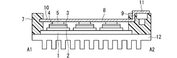
- FIG. 2 is a sectional view taken along line A1-A2 in FIG. 1.
- FIG. 9 is a plan view showing an example of a configuration of a semiconductor device according to a second embodiment of the present invention.
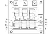
- FIG. 4 is a sectional view taken along line B1-B2 in FIG. 3.
- FIG. 9 is a plan view showing an example of a configuration of a semiconductor device according to a third embodiment of the present invention.
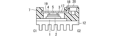
- FIG. 6 is a cross-sectional view of C1-C2 in FIG.
- FIG. 14 is a plan view showing an example of a configuration of a semiconductor device according to a fourth embodiment of the present invention.
- FIG. 8 is a sectional view taken along the line D1-D2 in FIG. 7.
- FIG. 16 is a plan view showing an example of a configuration of a semiconductor device according to a fifth embodiment of the present invention.
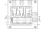
- FIG. 10 is a sectional view taken along line E1-E2 in FIG. 9. It is a top view which shows an example of a structure of the semiconductor device by related technology. It is a figure which shows an example of the cross section of F1-F2 in FIG. It is a figure which shows an example of the cross section of F1-F2 in FIG. It is a figure which shows an example of the cross section of F1-F2 in FIG. It is a top view which shows an example of a structure of the semiconductor device by related technology.
- FIG. 11 is a plan view showing an example of the configuration of a semiconductor device according to related technology.
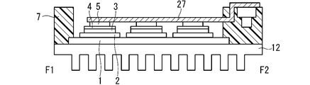
- FIG. 12 is a diagram showing an example of a cross section taken along line F1-F2 of FIG. 11 and 12 show a state before the resin is injected into the resin case 7.
- the semiconductor device shown in FIGS. 11 and 12 has a circuit pattern 2 provided on a substrate 1.
- Semiconductor elements 4 and 6 are bonded onto the circuit pattern 2 via solder 3.
- a heat sink 12 is provided on the back surface of the substrate 1.
- a resin case 7 is provided on the periphery of the substrate 1.
- a wiring member 27 is integrally formed with the resin case 7. The wiring member 27 is joined to the surfaces of the semiconductor elements 4 and 6 opposite to the substrate 1 via the solder 5, and one end thereof is exposed to the outside of the resin case 7.
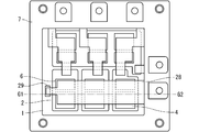
- FIG. 15 is a plan view showing an example of the configuration of a semiconductor device according to related technology.
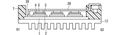
- FIG. 16 is a diagram showing an example of a cross section taken along G1-G2 in FIG. 15 and 16 show a state before the resin is injected into the resin case 7.
- the semiconductor device shown in FIGS. 15 and 16 has a circuit pattern 29 provided on the substrate 1.
- the circuit pattern 29 is insulated from the circuit pattern 2.
- a part of the wiring member 28 extends toward the substrate 1 and is in contact with the circuit pattern 29.
- the circuit pattern 29 may be a protrusion.
- Other configurations are the same as those of the semiconductor device shown in FIGS. 11 and 12, and thus detailed description thereof is omitted here.
- FIG. 17 is a plan view showing an example of the configuration of a semiconductor device according to related technology.
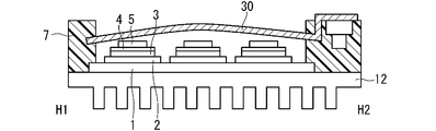
- FIG. 18 is a diagram showing an example of a cross section taken along line H1-H2 in FIG. 17 and 18 show a state before the resin is injected into the resin case 7.
- one end of the wiring member 30 is exposed from the inside of the wall surface of the resin case 7, and the other end is fixed inside the wall surface of the resin case 7.
- Other configurations are the same as those of the semiconductor device shown in FIGS. 11 and 12, and thus detailed description thereof is omitted here.
- FIG. 20 is a plan view showing an example of the configuration of a semiconductor device according to related technology.
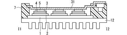
- 21 is a diagram showing an example of a cross section taken along line I1-I2 of FIG. 20 and 21 show a state before the resin is injected into the resin case 7.
- the wiring member 31 in the resin case 7 is bent.
- Other configurations are similar to those of the semiconductor device shown in FIGS. 17 and 18, and thus detailed description thereof is omitted here.
- FIG. 1 is a plan view showing an example of the configuration of the semiconductor device according to the first embodiment.
- FIG. 2 is a sectional view taken along line A1-A2 in FIG. 1 and 2 show a state before the resin is injected into the resin case 7.
- the semiconductor device according to the first embodiment is characterized by the second fixing portion 10 of the wiring member 8.
- Other configurations are the same as those of the semiconductor device according to the related art shown in FIGS. 11 and 12, and thus detailed description thereof is omitted here.
- the wiring member 8 is provided with respect to an exposed portion 11 adjacent to the first fixing portion 9 fixed inside the wall surface of the resin case 7 and exposed to the outside, and a portion extending from the first fixing portion 9 into the resin case 7.
- a second fixing portion 10 fixed in the wall surface of the resin case 7 at a position different from the first fixing portion 9, and on the surface of the semiconductor elements 4, 6 opposite to the substrate 1 in the resin case 7. Is a plate shape having a length, a thickness, and a width, which are joined to each other with solder 5.
- the wiring member 8 has a uniform thickness and is flat inside the resin case 7, and is not bent. Further, the second fixing portion 10 of the wiring member 8 is formed by punching so that the width becomes narrow. Therefore, the width of the second fixing portion 10 is narrower than the width of the exposed portion 11.
- the wiring member and the semiconductor element are joined by solder at a high temperature of about 200 ° C to 250 ° C.
- the resin case and the wiring member are also in a high temperature state, but since the respective linear expansion coefficients are different, strain is generated between the resin case and the wiring member.
- the semiconductor device according to the first embodiment since the width of the second fixing portion 10 of the wiring member 8 is narrowed to facilitate the deformation, the strain generated at the high temperature of the second fixing portion 10 is relaxed.
- the strain generated in the second fixing portion 10 of the wiring member 8 at high temperature is relaxed, the position of the wiring member 8 in the height direction does not shift. Therefore, the accuracy of the position of the wiring member 8 in the height direction can be improved. Further, since the accuracy of the position of the wiring member 8 in the height direction is improved, the bonding state of the wiring member 8 and the semiconductor elements 4 and 6 with the solder 5 becomes good. Further, since the wiring member 8 is not bent, the cost of the wiring member 8 can be suppressed.
- FIG. 3 is a plan view showing an example of the configuration of the semiconductor device according to the second embodiment.
- FIG. 4 is a sectional view taken along line B1-B2 in FIG. 3 and 4 show a state before the resin is injected into the resin case 7.
- the semiconductor device according to the second embodiment is characterized by the second fixing portion 15 of the wiring member 13.
- the first fixing portion 14 of the wiring member 13 corresponds to the first fixing portion 9 of FIGS. 1 and 2
- the exposed portion 16 of the wiring member 13 corresponds to the exposed portion 11 of FIGS.
- Other configurations are similar to those of the semiconductor device according to the first embodiment shown in FIGS. 1 and 2, and therefore detailed description thereof will be omitted here.
- the second fixing portion 15 has a bent shape in plan view. Specifically, the second fixing portion 15 has a crank shape. It should be noted that the examples of FIGS. 3 and 4 show the case where the second fixing portion 15 has a crank shape, but the present invention is not limited to this. For example, the second fixing portion 15 may have a curved shape.
- the second embodiment by making the second fixing portion 15 of the wiring member 13 into the bent shape, it is possible to enhance the effect of alleviating the strain more than the semiconductor device according to the first embodiment. .
- FIG. 5 is a plan view showing an example of the configuration of the semiconductor device according to the third embodiment.
- FIG. 6 is a cross-sectional view of C1-C2 in FIG. 5 and 6 show a state before the resin is injected into the resin case 7.
- the semiconductor device according to the third embodiment is characterized by the second fixing portion 19 of the wiring member 17.
- the first fixing portion 18 of the wiring member 17 corresponds to the first fixing portion 9 of FIGS. 1 and 2
- the exposed portion 20 of the wiring member 17 corresponds to the exposed portion 11 of FIGS.
- Other configurations are similar to those of the semiconductor device according to the first embodiment shown in FIGS. 1 and 2, and therefore detailed description thereof will be omitted here.
- the second fixing portion 19 of the wiring member 17 is fixed in the wall surface adjacent to the wall surface of the resin case 7 to which the first fixing portion 18 is fixed.
- the strain generated in the second fixing portion 19 at high temperature is relaxed, the position of the wiring member 17 in the height direction does not shift. Therefore, the accuracy of the position of the wiring member 17 in the height direction can be improved.
- FIG. 7 is a plan view showing an example of the configuration of the semiconductor device according to the fourth embodiment.
- FIG. 8 is a sectional view taken along line D1-D2 in FIG. 7 and 8 show a state before the resin is injected into the resin case 7.
- the semiconductor device according to the fourth embodiment is characterized by the resin case 7 and the wiring member 22.
- Other configurations are the same as those of the semiconductor device according to the related art shown in FIGS. 11 and 12, and thus detailed description thereof is omitted here.
- the resin case 7 is provided on the peripheral edge of the substrate 1 and has a protruding portion 21 partially protruding inward.
- the wiring member 22 is fixed to the protrusion 21 at a location different from the exposed portion 25 adjacent to the first fixing portion 23 fixed inside the wall surface of the resin case 7 and exposed to the outside, and the first fixing portion 23. It has a second fixing portion 24, is joined to the surfaces of the semiconductor elements 4 and 6 opposite to the substrate 1 with solder 5, and has a plate shape having a length, a thickness, and a width.
- the wiring member 22 has a uniform thickness and is flat in the resin case 7, and is not bent.
- the protrusion 21 of the resin case 7 relieves the strain generated when the temperature is high, the position of the wiring member 22 in the height direction does not shift. Therefore, the accuracy of the position of the wiring member 22 in the height direction can be improved. Further, since the accuracy of the position of the wiring member 22 in the height direction is improved, the bonding state of the wiring member 22 and the semiconductor elements 4 and 6 with the solder 5 becomes good. Further, since the wiring member 22 is not bent, the cost of the wiring member 22 can be suppressed and the processing of the wiring member 22 becomes easy.
- FIG. 9 is a plan view showing an example of the configuration of the semiconductor device according to the fifth embodiment.
- FIG. 10 is a sectional view taken along line E1-E2 in FIG. 9 and 10 show a state before the resin is injected into the resin case 7.
- the semiconductor device according to the fifth embodiment is characterized by the resin case 7.
- Other structures are similar to those of the semiconductor device according to the fourth embodiment shown in FIGS. 7 and 8, and therefore detailed description thereof is omitted here.
- the protrusion 26 of the resin case 7 has a bent shape in plan view. Specifically, the protrusion 26 has a crank shape. 9 and 10 show the case where the protrusion 26 has a crank shape, the present invention is not limited to this. For example, the protrusion 26 may have a curved shape.
Landscapes
- Structures Or Materials For Encapsulating Or Coating Semiconductor Devices Or Solid State Devices (AREA)
- Physics & Mathematics (AREA)
- Geometry (AREA)
Abstract
本発明は、配線部材の高さ方向の位置の精度を向上させることが可能な半導体装置を提供することを目的とする。本発明による半導体装置は、半導体素子(4)が設けられた基板(1)と、基板(1)の周縁に設けられた樹脂ケース(7)と、樹脂ケース(7)の壁面内に固定された第1固定部(9)に隣接して外部に露出した露出部(11)と、第1固定部(9)から樹脂ケース(7)内に延在する部分に対し第1固定部(9)とは異なる箇所で樹脂ケース(7)の壁面内に固定された第2固定部(10)とを有し、樹脂ケース(7)内において半導体素子(4)の基板(1)とは反対側の面上にはんだ(5)で接合され、長さ、厚み、および幅を有する板形状の配線部材(8)とを備え、配線部材(8)は、樹脂ケース(7)内において厚みが均一で平坦であり、かつ第2固定部(10)の幅が露出部(11)の幅よりも狭い。
Description
本発明は、半導体装置に関し、特に、電気自動車または電車等のモータを制御するインバータ、または回生用のコンバータ等に用いられる半導体装置に関する。
従来、樹脂ケースに一体成形された配線部材を備える半導体装置が開示されている(例えば、特許文献1,2参照)。配線部材は、半導体素子の上面に設けられた電極にはんだで接合され、一部が外部に露出している。このような構成において、配線部材と半導体素子とのはんだによる接合を良好な状態にするためには、配線部材の高さ方向の精度を良くする必要がある。ここで、配線部材の高さ方向とは、配線部材と半導体素子との間隔方向のことをいう。
半導体装置の製造工程において、配線部材と半導体素子とは、約200℃~250℃の高温状態ではんだによって接合される。このとき、樹脂ケースおよび配線部材も高温状態となるが、それぞれの線膨張係数が異なるため、樹脂ケースと配線部材との間でひずみが発生する。
特許文献1,2では、上記のひずみを緩和するために、配線部材に折り曲げ加工を施している。しかし、折り曲げ加工を施した配線部材は、高さ方向の位置の精度が良くないため、配線部材と半導体素子とをはんだで良好に接合することができないことがある。
本発明は、このような問題を解決するためになされたものであり、配線部材の高さ方向の位置の精度を向上させることが可能な半導体装置を提供することを目的とする。
上記の課題を解決するために、本発明による半導体装置は、半導体素子が設けられた基板と、基板の周縁に設けられた樹脂ケースと、樹脂ケースの壁面内に固定された第1固定部に隣接して外部に露出した露出部と、第1固定部から樹脂ケース内に延在する部分に対し第1固定部とは異なる箇所で樹脂ケースの壁面内に固定された第2固定部とを有し、樹脂ケース内において半導体素子の基板とは反対側の面上にはんだで接合され、長さ、厚み、および幅を有する板形状の配線部材とを備え、配線部材は、樹脂ケース内において厚みが均一で平坦であり、かつ第2固定部の幅が露出部の幅よりも狭い。
本発明によると、半導体装置は、半導体素子が設けられた基板と、基板の周縁に設けられた樹脂ケースと、樹脂ケースの壁面内に固定された第1固定部に隣接して外部に露出した露出部と、第1固定部から樹脂ケース内に延在する部分に対し第1固定部とは異なる箇所で樹脂ケースの壁面内に固定された第2固定部とを有し、樹脂ケース内において半導体素子の基板とは反対側の面上にはんだで接合され、長さ、厚み、および幅を有する板形状の配線部材とを備え、配線部材は、樹脂ケース内において厚みが均一で平坦であり、かつ第2固定部の幅が露出部の幅よりも狭いため、配線部材の高さ方向の位置の精度を向上させることが可能となる。
本発明の目的、特徴、態様、および利点は、以下の詳細な説明と添付図面とによって、より明白となる。
本発明の実施の形態について、図面に基づいて以下に説明する。
<関連技術>
まず、本実施の形態の関連技術について説明する。
まず、本実施の形態の関連技術について説明する。
図11は、関連技術による半導体装置の構成の一例を示す平面図である。図12は、図11におけるF1-F2の断面の一例を示す図である。なお、図11,12は、樹脂ケース7内に樹脂を注入する前の状態を示している。
図11,12に示す半導体装置は、基板1上に回路パターン2を設けている。回路パターン2上には、はんだ3を介して半導体素子4,6が接合されている。また、基板1の裏面には、ヒートシンク12が設けられている。
基板1の周縁には、樹脂ケース7が設けられている。樹脂ケース7には、配線部材27が一体成形されている。配線部材27は、半導体素子4,6の基板1とは反対側の面上に、はんだ5を介して接合され、一端が樹脂ケース7の外部に露出している。
図11,12に示す半導体装置の構成では、配線部材27の高さ方向の位置の精度にばらつきが生じる。図12の例では、配線部材27の高さ方向の位置が適切であるため、配線部材27と半導体素子4,6とのはんだ5による接合状態は良好である。しかし、図13,14に示すように、配線部材27の高さ方向の位置が適切でないとき、配線部材27と半導体素子4,6とのはんだ5による接合状態が悪くなる。
具体的には、図13の例では、配線部材27と半導体素子4との間隔が大きくなる箇所があり、このような箇所では配線部材27と半導体素子4とをはんだ5で接合することができない。また、図14の例では、配線部材27と半導体素子4との間隔が小さくなる箇所があり、このような箇所では配線部材27と半導体素子4との接合時にはんだ5がはみ出てしまう。
図15は、関連技術による半導体装置の構成の一例を示す平面図である。図16は、図15におけるG1-G2の断面の一例を示す図である。なお、図15,16は、樹脂ケース7内に樹脂を注入する前の状態を示している。
図15,16に示す半導体装置は、基板1上に回路パターン29を設けている。回路パターン29は、回路パターン2とは絶縁されている。配線部材28は、その一部が基板1に向けて延設されており、回路パターン29に接触している。なお、回路パターン29は、突起であってもよい。その他の構成は、図11,12に示す半導体装置と同様であるため、ここでは詳細な説明を省略する。
図15,16に示す半導体装置の構成は、配線部材28の高さ方向の位置を制御することは可能であるが、回路パターン29を設けるスペースと、回路パターン29と回路パターン2とを絶縁するためのスペースとが必要である。従って、図15,16に示す半導体装置は、小型化が困難である。
図17は、関連技術による半導体装置の構成の一例を示す平面図である。図18は、図17におけるH1-H2の断面の一例を示す図である。なお、図17,18は、樹脂ケース7内に樹脂を注入する前の状態を示している。
図17,18に示す半導体装置は、配線部材30の一端が樹脂ケース7の壁面内から外部に露出し、他端が樹脂ケース7の壁面内に固定されている。その他の構成は、図11,12に示す半導体装置と同様であるため、ここでは詳細な説明を省略する。
図17,18に示す半導体装置の構成では、高温状態で配線部材30と半導体素子4とをはんだ5で接合するときに、樹脂ケース7と配線部材30との間でひずみが発生する。これにより、図19に示すように、配線部材30が湾曲してしまう。配線部材30が湾曲すると、配線部材30の高さ方向の位置にばらつきが生じ、配線部材30と半導体素子4とをはんだ5で接合することができない。
図20は、関連技術による半導体装置の構成の一例を示す平面図である。図21は、図20におけるI1-I2の断面の一例を示す図である。なお、図20,21は、樹脂ケース7内に樹脂を注入する前の状態を示している。
図20,21に示す半導体装置は、樹脂ケース7における配線部材31に折り曲げ加工を施している。その他の構成は、図17,18に示す半導体装置と同様であるため、ここでは詳細な説明を省略する。
図20,21に示す半導体装置の構成では、高温状態で配線部材31と半導体素子4とをはんだ5で接合するときに、樹脂ケース7と配線部材31との間で発生するひずみを緩和することができる。しかし、折り曲げ加工を施した配線部材31は、高さ方向の位置の精度が良くないため、配線部材31と半導体素子4とをはんだ5で良好に接合することができないことがある。また、配線部材31に折り曲げ加工を施すためのコストがかかる。
このように、上記で説明した関連技術による半導体装置では、配線部材の高さ方向の位置の精度を向上させているとはいえなかった。本実施の形態は、上記の関連技術による半導体装置の問題を解決するためになされたものであり、以下に詳細に説明する。
<実施の形態1>
図1は、本実施の形態1による半導体装置の構成の一例を示す平面図である。図2は、図1におけるA1-A2の断面図である。なお、図1,2は、樹脂ケース7内に樹脂を注入する前の状態を示している。
図1は、本実施の形態1による半導体装置の構成の一例を示す平面図である。図2は、図1におけるA1-A2の断面図である。なお、図1,2は、樹脂ケース7内に樹脂を注入する前の状態を示している。
図1,2に示すように、本実施の形態1による半導体装置は、配線部材8の第2固定部10に特徴を有している。その他の構成は、図11,12に示す関連技術による半導体装置と同様であるため、ここでは詳細な説明を省略する。
配線部材8は、樹脂ケース7の壁面内に固定された第1固定部9に隣接して外部に露出した露出部11と、第1固定部9から樹脂ケース7内に延在する部分に対し第1固定部9とは異なる箇所で樹脂ケース7の壁面内に固定された第2固定部10とを有し、樹脂ケース7内において半導体素子4,6の基板1とは反対側の面上にはんだ5で接合され、長さ、厚み、および幅を有する板形状である。また、配線部材8は、樹脂ケース7内において厚みが均一で平坦であり、折り曲げ加工が施されていない。さらに、配線部材8の第2固定部10は、幅が狭くなるように打ち抜き加工によって形成されている。従って、第2固定部10の幅は、露出部11の幅よりも狭い。
上述の通り、半導体装置の製造工程において、配線部材と半導体素子とは、約200℃~250℃の高温状態ではんだによって接合される。このとき、樹脂ケースおよび配線部材も高温状態となるが、それぞれの線膨張係数が異なるため、樹脂ケースと配線部材との間でひずみが発生する。一方、本実施の形態1による半導体装置では、配線部材8の第2固定部10の幅を狭くして変形しやすくしているため、第2固定部10が高温時に発生するひずみを緩和する。
以上のことから、本実施の形態1によれば、配線部材8の第2固定部10が高温時に発生するひずみを緩和するため、配線部材8の高さ方向の位置がずれることはない。従って、配線部材8の高さ方向の位置の精度を向上させることが可能となる。また、配線部材8の高さ方向の位置の精度が向上するため、配線部材8と半導体素子4,6とのはんだ5による接合状態が良好となる。さらに、配線部材8に折り曲げ加工を施していないため、配線部材8にかかるコストを抑えることができる。
<実施の形態2>
図3は、本実施の形態2による半導体装置の構成の一例を示す平面図である。図4は、図3におけるB1-B2の断面図である。なお、図3,4は、樹脂ケース7内に樹脂を注入する前の状態を示している。
図3は、本実施の形態2による半導体装置の構成の一例を示す平面図である。図4は、図3におけるB1-B2の断面図である。なお、図3,4は、樹脂ケース7内に樹脂を注入する前の状態を示している。
図3,4に示すように、本実施の形態2による半導体装置は、配線部材13の第2固定部15に特徴を有している。なお、配線部材13の第1固定部14は図1,2の第1固定部9に相当し、配線部材13の露出部16は図1,2の露出部11に相当する。その他の構成は、図1,2に示す実施の形態1による半導体装置と同様であるため、ここでは詳細な説明を省略する。
配線部材13は、第2固定部15が平面視において屈曲形状となっている。具体的には、第2固定部15は、クランク形状である。なお、図3,4の例では、第2固定部15がクランク形状である場合について示しているが、これに限るものではない。例えば、第2固定部15は、湾曲形状であってもよい。
以上のことから、本実施の形態2によれば、配線部材13の第2固定部15を屈曲形状とすることによって、実施の形態1による半導体装置よりもひずみを緩和する効果を高めることができる。
<実施の形態3>
図5は、本実施の形態3による半導体装置の構成の一例を示す平面図である。図6は、図5におけるC1-C2の断面図である。なお、図5,6は、樹脂ケース7内に樹脂を注入する前の状態を示している。
図5は、本実施の形態3による半導体装置の構成の一例を示す平面図である。図6は、図5におけるC1-C2の断面図である。なお、図5,6は、樹脂ケース7内に樹脂を注入する前の状態を示している。
図5,6に示すように、本実施の形態3による半導体装置は、配線部材17の第2固定部19に特徴を有している。なお、配線部材17の第1固定部18は図1,2の第1固定部9に相当し、配線部材17の露出部20は図1,2の露出部11に相当する。その他の構成は、図1,2に示す実施の形態1による半導体装置と同様であるため、ここでは詳細な説明を省略する。
配線部材17の第2固定部19は、第1固定部18が固定されている樹脂ケース7の壁面に隣接する壁面内に固定されている。
以上のことから、本実施の形態3によれば、第2固定部19が高温時に発生するひずみを緩和するため、配線部材17の高さ方向の位置がずれることはない。従って、配線部材17の高さ方向の位置の精度を向上させることが可能となる。
<実施の形態4>
図7は、本実施の形態4による半導体装置の構成の一例を示す平面図である。図8は、図7におけるD1-D2の断面図である。なお、図7,8は、樹脂ケース7内に樹脂を注入する前の状態を示している。
図7は、本実施の形態4による半導体装置の構成の一例を示す平面図である。図8は、図7におけるD1-D2の断面図である。なお、図7,8は、樹脂ケース7内に樹脂を注入する前の状態を示している。
図7,8に示すように、本実施の形態4による半導体装置は、樹脂ケース7および配線部材22に特徴を有している。その他の構成は、図11,12に示す関連技術による半導体装置と同様であるため、ここでは詳細な説明を省略する。
樹脂ケース7は、基板1の周縁に設けられ、一部が内側に突出した突起部21を有している。
配線部材22は、樹脂ケース7の壁面内に固定された第1固定部23に隣接して外部に露出した露出部25と、第1固定部23とは異なる箇所で突起部21に固定された第2固定部24とを有し、半導体素子4,6の基板1とは反対側の面上にはんだ5で接合され、長さ、厚み、および幅を有する板形状である。また、配線部材22は、樹脂ケース7内において厚みが均一で平坦であり、折り曲げ加工が施されていない。
以上のことから、本実施の形態4によれば、樹脂ケース7の突起部21が高温時に発生するひずみを緩和するため、配線部材22の高さ方向の位置がずれることはない。従って、配線部材22の高さ方向の位置の精度を向上させることが可能となる。また、配線部材22の高さ方向の位置の精度が向上するため、配線部材22と半導体素子4,6とのはんだ5による接合状態が良好となる。さらに、配線部材22に折り曲げ加工を施していないため配線部材22にかかるコストを抑えることができ、配線部材22の加工が容易となる。
<実施の形態5>
図9は、本実施の形態5による半導体装置の構成の一例を示す平面図である。図10は、図9におけるE1-E2の断面図である。なお、図9,10は、樹脂ケース7内に樹脂を注入する前の状態を示している。
図9は、本実施の形態5による半導体装置の構成の一例を示す平面図である。図10は、図9におけるE1-E2の断面図である。なお、図9,10は、樹脂ケース7内に樹脂を注入する前の状態を示している。
図9,10に示すように、本実施の形態5による半導体装置は、樹脂ケース7に特徴を有している。その他の構成は、図7,8に示す実施の形態4による半導体装置と同様であるため、ここでは詳細な説明を省略する。
樹脂ケース7の突起部26は、平面視において屈曲形状となっている。具体的には、突起部26は、クランク形状である。なお、図9,10の例では、突起部26がクランク形状である場合について示しているが、これに限るものではない。例えば、突起部26は、湾曲形状であってもよい。
以上のことから、本実施の形態5によれば、樹脂ケース7の突起部26を屈曲形状とすることによって、実施の形態4による半導体装置よりもひずみを緩和する効果を高めることができる。
なお、本発明は、その発明の範囲内において、各実施の形態を自由に組み合わせたり、各実施の形態を適宜、変形、省略することが可能である。
本発明は詳細に説明されたが、上記した説明は、すべての態様において、例示であって、この発明がそれに限定されるものではない。例示されていない無数の変形例が、この発明の範囲から外れることなく想定され得るものと解される。
1 基板、2 回路パターン、3 はんだ、4 半導体素子、5 はんだ、6 半導体素子、7 樹脂ケース、8 配線部材、9 第1固定部、10 第2固定部、11 露出部、12 ヒートシンク、13 配線部材、14 第1固定部、15 第2固定部、16 露出部、17 配線部材、18 第1固定部、19 第2固定部、20 露出部、21 突起部、22 配線部材、23 第1固定部、24 第2固定部、25 露出部、26 突起部、27,28 配線部材、29 回路パターン、30,31 配線部材。
Claims (5)
- 半導体素子(4)が設けられた基板(1)と、
前記基板(1)の周縁に設けられた樹脂ケース(7)と、
前記樹脂ケース(7)の壁面内に固定された第1固定部(9)に隣接して外部に露出した露出部(11)と、前記第1固定部(9)から前記樹脂ケース(7)内に延在する部分に対し前記第1固定部(9)とは異なる箇所で前記樹脂ケース(7)の壁面内に固定された第2固定部(10)とを有し、前記樹脂ケース(7)内において前記半導体素子(4)の前記基板(1)とは反対側の面上にはんだ(5)で接合され、長さ、厚み、および幅を有する板形状の配線部材(8)と、
を備え、
前記配線部材(8)は、前記樹脂ケース(7)内において前記厚みが均一で平坦であり、かつ前記第2固定部(10)の前記幅が前記露出部(11)の前記幅よりも狭いことを特徴とする、半導体装置。 - 前記第2固定部(10)は、平面視において屈曲形状であることを特徴とする、請求項1に記載の半導体装置。
- 前記第2固定部(10)は、前記第1固定部(9)が固定されている前記樹脂ケース(7)の壁面に隣接する壁面内に固定されることを特徴とする、請求項1に記載の半導体装置。
- 半導体素子(4)が設けられた基板(1)と、
前記基板(1)の周縁に設けられ、一部が内側に突出した突起部(21)を有する樹脂ケース(7)と、
前記樹脂ケース(7)の壁面内に固定された第1固定部(23)に隣接して外部に露出した露出部(25)と、前記第1固定部(23)とは異なる箇所で前記突起部(21)に固定された第2固定部(24)とを有し、前記半導体素子(4)の前記基板(1)とは反対側の面上にはんだ(5)で接合され、長さ、厚み、および幅を有する板形状の配線部材(22)と、
を備え、
前記配線部材(22)は、前記樹脂ケース(7)内において前記厚みが均一で平坦であることを特徴とする、半導体装置。 - 前記突起部(21)は、平面視において屈曲形状であることを特徴とする、請求項4に記載の半導体装置。
Priority Applications (5)
| Application Number | Priority Date | Filing Date | Title |
|---|---|---|---|
| DE112018008155.9T DE112018008155T5 (de) | 2018-11-20 | 2018-11-20 | Halbleitervorrichtung |
| JP2020557062A JP7005790B2 (ja) | 2018-11-20 | 2018-11-20 | 半導体装置 |
| US17/269,480 US11562977B2 (en) | 2018-11-20 | 2018-11-20 | Semiconductor device comprising a resin case and a wiring member that is flat in the resin case |
| CN201880099541.0A CN113039637A (zh) | 2018-11-20 | 2018-11-20 | 半导体装置 |
| PCT/JP2018/042805 WO2020105114A1 (ja) | 2018-11-20 | 2018-11-20 | 半導体装置 |
Applications Claiming Priority (1)
| Application Number | Priority Date | Filing Date | Title |
|---|---|---|---|
| PCT/JP2018/042805 WO2020105114A1 (ja) | 2018-11-20 | 2018-11-20 | 半導体装置 |
Publications (1)
| Publication Number | Publication Date |
|---|---|
| WO2020105114A1 true WO2020105114A1 (ja) | 2020-05-28 |
Family
ID=70773379
Family Applications (1)
| Application Number | Title | Priority Date | Filing Date |
|---|---|---|---|
| PCT/JP2018/042805 Ceased WO2020105114A1 (ja) | 2018-11-20 | 2018-11-20 | 半導体装置 |
Country Status (5)
| Country | Link |
|---|---|
| US (1) | US11562977B2 (ja) |
| JP (1) | JP7005790B2 (ja) |
| CN (1) | CN113039637A (ja) |
| DE (1) | DE112018008155T5 (ja) |
| WO (1) | WO2020105114A1 (ja) |
Citations (6)
| Publication number | Priority date | Publication date | Assignee | Title |
|---|---|---|---|---|
| JPH0645518A (ja) * | 1992-07-24 | 1994-02-18 | Fuji Electric Co Ltd | パワー半導体装置 |
| JP2009105267A (ja) * | 2007-10-24 | 2009-05-14 | Fuji Electric Device Technology Co Ltd | 半導体装置およびその製造方法 |
| WO2013058038A1 (ja) * | 2011-10-18 | 2013-04-25 | 富士電機株式会社 | 半導体装置および半導体装置製造方法 |
| WO2014049740A1 (ja) * | 2012-09-26 | 2014-04-03 | トヨタ自動車株式会社 | 電気部品 |
| JP2015046416A (ja) * | 2013-08-27 | 2015-03-12 | 三菱電機株式会社 | 半導体装置および半導体装置の製造方法 |
| WO2017169134A1 (ja) * | 2016-03-30 | 2017-10-05 | 三菱電機株式会社 | パワーモジュール及びその製造方法並びにパワーエレクトロニクス機器及びその製造方法 |
Family Cites Families (3)
| Publication number | Priority date | Publication date | Assignee | Title |
|---|---|---|---|---|
| JP4722415B2 (ja) * | 2004-06-14 | 2011-07-13 | 三菱電機株式会社 | 半導体装置およびその製造方法 |
| JP6201626B2 (ja) * | 2013-10-23 | 2017-09-27 | スミダコーポレーション株式会社 | 電子部品及び電子部品の製造方法 |
| JP6293030B2 (ja) * | 2014-10-09 | 2018-03-14 | 三菱電機株式会社 | 電力用半導体装置 |
-
2018
- 2018-11-20 US US17/269,480 patent/US11562977B2/en active Active
- 2018-11-20 CN CN201880099541.0A patent/CN113039637A/zh active Pending
- 2018-11-20 WO PCT/JP2018/042805 patent/WO2020105114A1/ja not_active Ceased
- 2018-11-20 JP JP2020557062A patent/JP7005790B2/ja active Active
- 2018-11-20 DE DE112018008155.9T patent/DE112018008155T5/de active Granted
Patent Citations (6)
| Publication number | Priority date | Publication date | Assignee | Title |
|---|---|---|---|---|
| JPH0645518A (ja) * | 1992-07-24 | 1994-02-18 | Fuji Electric Co Ltd | パワー半導体装置 |
| JP2009105267A (ja) * | 2007-10-24 | 2009-05-14 | Fuji Electric Device Technology Co Ltd | 半導体装置およびその製造方法 |
| WO2013058038A1 (ja) * | 2011-10-18 | 2013-04-25 | 富士電機株式会社 | 半導体装置および半導体装置製造方法 |
| WO2014049740A1 (ja) * | 2012-09-26 | 2014-04-03 | トヨタ自動車株式会社 | 電気部品 |
| JP2015046416A (ja) * | 2013-08-27 | 2015-03-12 | 三菱電機株式会社 | 半導体装置および半導体装置の製造方法 |
| WO2017169134A1 (ja) * | 2016-03-30 | 2017-10-05 | 三菱電機株式会社 | パワーモジュール及びその製造方法並びにパワーエレクトロニクス機器及びその製造方法 |
Also Published As
| Publication number | Publication date |
|---|---|
| CN113039637A (zh) | 2021-06-25 |
| US20210313295A1 (en) | 2021-10-07 |
| DE112018008155T5 (de) | 2021-07-29 |
| JPWO2020105114A1 (ja) | 2021-04-08 |
| US11562977B2 (en) | 2023-01-24 |
| JP7005790B2 (ja) | 2022-01-24 |
Similar Documents
| Publication | Publication Date | Title |
|---|---|---|
| JP6305302B2 (ja) | 半導体装置およびその製造方法 | |
| JP6299120B2 (ja) | 半導体モジュール | |
| JP4858336B2 (ja) | 電力用半導体装置 | |
| US9917064B2 (en) | Semiconductor device with a plate-shaped lead terminal | |
| WO2016084483A1 (ja) | リードフレーム、半導体装置、リードフレームの製造方法、および半導体装置の製造方法 | |
| US10886205B2 (en) | Terminal structure and semiconductor module | |
| JP6365768B2 (ja) | 半導体装置 | |
| JP5136748B2 (ja) | 素子の位置決め治具及び実装方法 | |
| JP6132034B2 (ja) | 半導体モジュール | |
| JP6092645B2 (ja) | 半導体装置 | |
| US7030491B2 (en) | Power semiconductor module with deflection-resistant base plate | |
| JP7005790B2 (ja) | 半導体装置 | |
| CN204706588U (zh) | 压电变压器装置 | |
| JP4848252B2 (ja) | 端子要素を備えたパワー半導体モジュール | |
| JP5793295B2 (ja) | 半導体装置 | |
| JP2013033784A (ja) | 電子制御装置 | |
| JP2014232832A (ja) | 電源装置およびビームリード | |
| JP2014216458A (ja) | ビームリードおよび電源装置 | |
| JP5603210B2 (ja) | シールドケース固定具 | |
| JP6523567B1 (ja) | 電子モジュール | |
| WO2023139687A1 (ja) | 半導体装置および半導体装置の製造方法 | |
| JP2011198929A (ja) | 半導体装置の内部接続構造、及び、半導体装置 | |
| JP2014216450A (ja) | ビームリードおよびパワーモジュール | |
| TWM441233U (en) | Electrical connector | |
| JP2009238840A (ja) | 基板の接続構造 |
Legal Events
| Date | Code | Title | Description |
|---|---|---|---|
| 121 | Ep: the epo has been informed by wipo that ep was designated in this application |
Ref document number: 18940549 Country of ref document: EP Kind code of ref document: A1 |
|
| ENP | Entry into the national phase |
Ref document number: 2020557062 Country of ref document: JP Kind code of ref document: A |
|
| 122 | Ep: pct application non-entry in european phase |
Ref document number: 18940549 Country of ref document: EP Kind code of ref document: A1 |