WO2020100947A1 - 半導体装置 - Google Patents
半導体装置 Download PDFInfo
- Publication number
- WO2020100947A1 WO2020100947A1 PCT/JP2019/044563 JP2019044563W WO2020100947A1 WO 2020100947 A1 WO2020100947 A1 WO 2020100947A1 JP 2019044563 W JP2019044563 W JP 2019044563W WO 2020100947 A1 WO2020100947 A1 WO 2020100947A1
- Authority
- WO
- WIPO (PCT)
- Prior art keywords
- electrode
- layer
- wiring
- semiconductor device
- resin
- Prior art date
- Legal status (The legal status is an assumption and is not a legal conclusion. Google has not performed a legal analysis and makes no representation as to the accuracy of the status listed.)
- Ceased
Links
Images











Classifications
-
- H—ELECTRICITY
- H10—SEMICONDUCTOR DEVICES; ELECTRIC SOLID-STATE DEVICES NOT OTHERWISE PROVIDED FOR
- H10W—GENERIC PACKAGES, INTERCONNECTIONS, CONNECTORS OR OTHER CONSTRUCTIONAL DETAILS OF DEVICES COVERED BY CLASS H10
- H10W72/00—Interconnections or connectors in packages
- H10W72/90—Bond pads, in general
-
- H—ELECTRICITY
- H10—SEMICONDUCTOR DEVICES; ELECTRIC SOLID-STATE DEVICES NOT OTHERWISE PROVIDED FOR
- H10W—GENERIC PACKAGES, INTERCONNECTIONS, CONNECTORS OR OTHER CONSTRUCTIONAL DETAILS OF DEVICES COVERED BY CLASS H10
- H10W74/00—Encapsulations, e.g. protective coatings
- H10W74/10—Encapsulations, e.g. protective coatings characterised by their shape or disposition
- H10W74/111—Encapsulations, e.g. protective coatings characterised by their shape or disposition the semiconductor body being completely enclosed
- H10W74/129—Encapsulations, e.g. protective coatings characterised by their shape or disposition the semiconductor body being completely enclosed forming a chip-scale package [CSP]
-
- H—ELECTRICITY
- H10—SEMICONDUCTOR DEVICES; ELECTRIC SOLID-STATE DEVICES NOT OTHERWISE PROVIDED FOR
- H10W—GENERIC PACKAGES, INTERCONNECTIONS, CONNECTORS OR OTHER CONSTRUCTIONAL DETAILS OF DEVICES COVERED BY CLASS H10
- H10W74/00—Encapsulations, e.g. protective coatings
- H10W74/10—Encapsulations, e.g. protective coatings characterised by their shape or disposition
- H10W74/111—Encapsulations, e.g. protective coatings characterised by their shape or disposition the semiconductor body being completely enclosed
- H10W74/114—Encapsulations, e.g. protective coatings characterised by their shape or disposition the semiconductor body being completely enclosed by a substrate and the encapsulations
- H10W74/117—Encapsulations, e.g. protective coatings characterised by their shape or disposition the semiconductor body being completely enclosed by a substrate and the encapsulations the substrate having spherical bumps for external connection
-
- H—ELECTRICITY
- H10—SEMICONDUCTOR DEVICES; ELECTRIC SOLID-STATE DEVICES NOT OTHERWISE PROVIDED FOR
- H10W—GENERIC PACKAGES, INTERCONNECTIONS, CONNECTORS OR OTHER CONSTRUCTIONAL DETAILS OF DEVICES COVERED BY CLASS H10
- H10W72/00—Interconnections or connectors in packages
- H10W72/01—Manufacture or treatment
- H10W72/012—Manufacture or treatment of bump connectors, dummy bumps or thermal bumps
-
- H—ELECTRICITY
- H10—SEMICONDUCTOR DEVICES; ELECTRIC SOLID-STATE DEVICES NOT OTHERWISE PROVIDED FOR
- H10W—GENERIC PACKAGES, INTERCONNECTIONS, CONNECTORS OR OTHER CONSTRUCTIONAL DETAILS OF DEVICES COVERED BY CLASS H10
- H10W72/00—Interconnections or connectors in packages
- H10W72/01—Manufacture or treatment
- H10W72/019—Manufacture or treatment of bond pads
- H10W72/01951—Changing the shapes of bond pads
-
- H—ELECTRICITY
- H10—SEMICONDUCTOR DEVICES; ELECTRIC SOLID-STATE DEVICES NOT OTHERWISE PROVIDED FOR
- H10W—GENERIC PACKAGES, INTERCONNECTIONS, CONNECTORS OR OTHER CONSTRUCTIONAL DETAILS OF DEVICES COVERED BY CLASS H10
- H10W72/00—Interconnections or connectors in packages
- H10W72/20—Bump connectors, e.g. solder bumps or copper pillars; Dummy bumps; Thermal bumps
-
- H—ELECTRICITY
- H10—SEMICONDUCTOR DEVICES; ELECTRIC SOLID-STATE DEVICES NOT OTHERWISE PROVIDED FOR
- H10W—GENERIC PACKAGES, INTERCONNECTIONS, CONNECTORS OR OTHER CONSTRUCTIONAL DETAILS OF DEVICES COVERED BY CLASS H10
- H10W72/00—Interconnections or connectors in packages
- H10W72/30—Die-attach connectors
-
- H—ELECTRICITY
- H10—SEMICONDUCTOR DEVICES; ELECTRIC SOLID-STATE DEVICES NOT OTHERWISE PROVIDED FOR
- H10W—GENERIC PACKAGES, INTERCONNECTIONS, CONNECTORS OR OTHER CONSTRUCTIONAL DETAILS OF DEVICES COVERED BY CLASS H10
- H10W72/00—Interconnections or connectors in packages
- H10W72/851—Dispositions of multiple connectors or interconnections
-
- H—ELECTRICITY
- H10—SEMICONDUCTOR DEVICES; ELECTRIC SOLID-STATE DEVICES NOT OTHERWISE PROVIDED FOR
- H10W—GENERIC PACKAGES, INTERCONNECTIONS, CONNECTORS OR OTHER CONSTRUCTIONAL DETAILS OF DEVICES COVERED BY CLASS H10
- H10W74/00—Encapsulations, e.g. protective coatings
- H10W74/01—Manufacture or treatment
- H10W74/014—Manufacture or treatment using batch processing
-
- H—ELECTRICITY
- H10—SEMICONDUCTOR DEVICES; ELECTRIC SOLID-STATE DEVICES NOT OTHERWISE PROVIDED FOR
- H10W—GENERIC PACKAGES, INTERCONNECTIONS, CONNECTORS OR OTHER CONSTRUCTIONAL DETAILS OF DEVICES COVERED BY CLASS H10
- H10W74/00—Encapsulations, e.g. protective coatings
- H10W74/40—Encapsulations, e.g. protective coatings characterised by their materials
-
- H—ELECTRICITY
- H10—SEMICONDUCTOR DEVICES; ELECTRIC SOLID-STATE DEVICES NOT OTHERWISE PROVIDED FOR
- H10W—GENERIC PACKAGES, INTERCONNECTIONS, CONNECTORS OR OTHER CONSTRUCTIONAL DETAILS OF DEVICES COVERED BY CLASS H10
- H10W74/00—Encapsulations, e.g. protective coatings
- H10W74/40—Encapsulations, e.g. protective coatings characterised by their materials
- H10W74/47—Encapsulations, e.g. protective coatings characterised by their materials comprising organic materials, e.g. plastics or resins
- H10W74/473—Encapsulations, e.g. protective coatings characterised by their materials comprising organic materials, e.g. plastics or resins containing a filler
-
- H—ELECTRICITY
- H10—SEMICONDUCTOR DEVICES; ELECTRIC SOLID-STATE DEVICES NOT OTHERWISE PROVIDED FOR
- H10W—GENERIC PACKAGES, INTERCONNECTIONS, CONNECTORS OR OTHER CONSTRUCTIONAL DETAILS OF DEVICES COVERED BY CLASS H10
- H10W20/00—Interconnections in chips, wafers or substrates
- H10W20/40—Interconnections external to wafers or substrates, e.g. back-end-of-line [BEOL] metallisations or vias connecting to gate electrodes
- H10W20/49—Adaptable interconnections, e.g. fuses or antifuses
-
- H—ELECTRICITY
- H10—SEMICONDUCTOR DEVICES; ELECTRIC SOLID-STATE DEVICES NOT OTHERWISE PROVIDED FOR
- H10W—GENERIC PACKAGES, INTERCONNECTIONS, CONNECTORS OR OTHER CONSTRUCTIONAL DETAILS OF DEVICES COVERED BY CLASS H10
- H10W70/00—Package substrates; Interposers; Redistribution layers [RDL]
- H10W70/01—Manufacture or treatment
- H10W70/05—Manufacture or treatment of insulating or insulated package substrates, or of interposers, or of redistribution layers
-
- H—ELECTRICITY
- H10—SEMICONDUCTOR DEVICES; ELECTRIC SOLID-STATE DEVICES NOT OTHERWISE PROVIDED FOR
- H10W—GENERIC PACKAGES, INTERCONNECTIONS, CONNECTORS OR OTHER CONSTRUCTIONAL DETAILS OF DEVICES COVERED BY CLASS H10
- H10W70/00—Package substrates; Interposers; Redistribution layers [RDL]
- H10W70/60—Insulating or insulated package substrates; Interposers; Redistribution layers
-
- H—ELECTRICITY
- H10—SEMICONDUCTOR DEVICES; ELECTRIC SOLID-STATE DEVICES NOT OTHERWISE PROVIDED FOR
- H10W—GENERIC PACKAGES, INTERCONNECTIONS, CONNECTORS OR OTHER CONSTRUCTIONAL DETAILS OF DEVICES COVERED BY CLASS H10
- H10W70/00—Package substrates; Interposers; Redistribution layers [RDL]
- H10W70/60—Insulating or insulated package substrates; Interposers; Redistribution layers
- H10W70/62—Insulating or insulated package substrates; Interposers; Redistribution layers characterised by their interconnections
- H10W70/65—Shapes or dispositions of interconnections
-
- H—ELECTRICITY
- H10—SEMICONDUCTOR DEVICES; ELECTRIC SOLID-STATE DEVICES NOT OTHERWISE PROVIDED FOR
- H10W—GENERIC PACKAGES, INTERCONNECTIONS, CONNECTORS OR OTHER CONSTRUCTIONAL DETAILS OF DEVICES COVERED BY CLASS H10
- H10W70/00—Package substrates; Interposers; Redistribution layers [RDL]
- H10W70/60—Insulating or insulated package substrates; Interposers; Redistribution layers
- H10W70/62—Insulating or insulated package substrates; Interposers; Redistribution layers characterised by their interconnections
- H10W70/65—Shapes or dispositions of interconnections
- H10W70/654—Top-view layouts
- H10W70/656—Fan-in layouts
-
- H—ELECTRICITY
- H10—SEMICONDUCTOR DEVICES; ELECTRIC SOLID-STATE DEVICES NOT OTHERWISE PROVIDED FOR
- H10W—GENERIC PACKAGES, INTERCONNECTIONS, CONNECTORS OR OTHER CONSTRUCTIONAL DETAILS OF DEVICES COVERED BY CLASS H10
- H10W70/00—Package substrates; Interposers; Redistribution layers [RDL]
- H10W70/60—Insulating or insulated package substrates; Interposers; Redistribution layers
- H10W70/62—Insulating or insulated package substrates; Interposers; Redistribution layers characterised by their interconnections
- H10W70/66—Conductive materials thereof
-
- H—ELECTRICITY
- H10—SEMICONDUCTOR DEVICES; ELECTRIC SOLID-STATE DEVICES NOT OTHERWISE PROVIDED FOR
- H10W—GENERIC PACKAGES, INTERCONNECTIONS, CONNECTORS OR OTHER CONSTRUCTIONAL DETAILS OF DEVICES COVERED BY CLASS H10
- H10W70/00—Package substrates; Interposers; Redistribution layers [RDL]
- H10W70/60—Insulating or insulated package substrates; Interposers; Redistribution layers
- H10W70/67—Insulating or insulated package substrates; Interposers; Redistribution layers characterised by their insulating layers or insulating parts
- H10W70/68—Shapes or dispositions thereof
-
- H—ELECTRICITY
- H10—SEMICONDUCTOR DEVICES; ELECTRIC SOLID-STATE DEVICES NOT OTHERWISE PROVIDED FOR
- H10W—GENERIC PACKAGES, INTERCONNECTIONS, CONNECTORS OR OTHER CONSTRUCTIONAL DETAILS OF DEVICES COVERED BY CLASS H10
- H10W72/00—Interconnections or connectors in packages
- H10W72/01—Manufacture or treatment
- H10W72/012—Manufacture or treatment of bump connectors, dummy bumps or thermal bumps
- H10W72/01251—Changing the shapes of bumps
- H10W72/01257—Changing the shapes of bumps by reflowing
-
- H—ELECTRICITY
- H10—SEMICONDUCTOR DEVICES; ELECTRIC SOLID-STATE DEVICES NOT OTHERWISE PROVIDED FOR
- H10W—GENERIC PACKAGES, INTERCONNECTIONS, CONNECTORS OR OTHER CONSTRUCTIONAL DETAILS OF DEVICES COVERED BY CLASS H10
- H10W72/00—Interconnections or connectors in packages
- H10W72/01—Manufacture or treatment
- H10W72/019—Manufacture or treatment of bond pads
-
- H—ELECTRICITY
- H10—SEMICONDUCTOR DEVICES; ELECTRIC SOLID-STATE DEVICES NOT OTHERWISE PROVIDED FOR
- H10W—GENERIC PACKAGES, INTERCONNECTIONS, CONNECTORS OR OTHER CONSTRUCTIONAL DETAILS OF DEVICES COVERED BY CLASS H10
- H10W72/00—Interconnections or connectors in packages
- H10W72/01—Manufacture or treatment
- H10W72/019—Manufacture or treatment of bond pads
- H10W72/01931—Manufacture or treatment of bond pads using blanket deposition
- H10W72/01933—Manufacture or treatment of bond pads using blanket deposition in liquid form, e.g. spin coating, spray coating or immersion coating
- H10W72/01935—Manufacture or treatment of bond pads using blanket deposition in liquid form, e.g. spin coating, spray coating or immersion coating by plating, e.g. electroless plating or electroplating
-
- H—ELECTRICITY
- H10—SEMICONDUCTOR DEVICES; ELECTRIC SOLID-STATE DEVICES NOT OTHERWISE PROVIDED FOR
- H10W—GENERIC PACKAGES, INTERCONNECTIONS, CONNECTORS OR OTHER CONSTRUCTIONAL DETAILS OF DEVICES COVERED BY CLASS H10
- H10W72/00—Interconnections or connectors in packages
- H10W72/01—Manufacture or treatment
- H10W72/019—Manufacture or treatment of bond pads
- H10W72/01931—Manufacture or treatment of bond pads using blanket deposition
- H10W72/01938—Manufacture or treatment of bond pads using blanket deposition in gaseous form, e.g. by CVD or PVD
-
- H—ELECTRICITY
- H10—SEMICONDUCTOR DEVICES; ELECTRIC SOLID-STATE DEVICES NOT OTHERWISE PROVIDED FOR
- H10W—GENERIC PACKAGES, INTERCONNECTIONS, CONNECTORS OR OTHER CONSTRUCTIONAL DETAILS OF DEVICES COVERED BY CLASS H10
- H10W72/00—Interconnections or connectors in packages
- H10W72/01—Manufacture or treatment
- H10W72/019—Manufacture or treatment of bond pads
- H10W72/01951—Changing the shapes of bond pads
- H10W72/01953—Changing the shapes of bond pads by etching
-
- H—ELECTRICITY
- H10—SEMICONDUCTOR DEVICES; ELECTRIC SOLID-STATE DEVICES NOT OTHERWISE PROVIDED FOR
- H10W—GENERIC PACKAGES, INTERCONNECTIONS, CONNECTORS OR OTHER CONSTRUCTIONAL DETAILS OF DEVICES COVERED BY CLASS H10
- H10W72/00—Interconnections or connectors in packages
- H10W72/01—Manufacture or treatment
- H10W72/019—Manufacture or treatment of bond pads
- H10W72/01951—Changing the shapes of bond pads
- H10W72/01955—Changing the shapes of bond pads by using masks
-
- H—ELECTRICITY
- H10—SEMICONDUCTOR DEVICES; ELECTRIC SOLID-STATE DEVICES NOT OTHERWISE PROVIDED FOR
- H10W—GENERIC PACKAGES, INTERCONNECTIONS, CONNECTORS OR OTHER CONSTRUCTIONAL DETAILS OF DEVICES COVERED BY CLASS H10
- H10W72/00—Interconnections or connectors in packages
- H10W72/01—Manufacture or treatment
- H10W72/0198—Manufacture or treatment batch processes
-
- H—ELECTRICITY
- H10—SEMICONDUCTOR DEVICES; ELECTRIC SOLID-STATE DEVICES NOT OTHERWISE PROVIDED FOR
- H10W—GENERIC PACKAGES, INTERCONNECTIONS, CONNECTORS OR OTHER CONSTRUCTIONAL DETAILS OF DEVICES COVERED BY CLASS H10
- H10W72/00—Interconnections or connectors in packages
- H10W72/20—Bump connectors, e.g. solder bumps or copper pillars; Dummy bumps; Thermal bumps
- H10W72/221—Structures or relative sizes
-
- H—ELECTRICITY
- H10—SEMICONDUCTOR DEVICES; ELECTRIC SOLID-STATE DEVICES NOT OTHERWISE PROVIDED FOR
- H10W—GENERIC PACKAGES, INTERCONNECTIONS, CONNECTORS OR OTHER CONSTRUCTIONAL DETAILS OF DEVICES COVERED BY CLASS H10
- H10W72/00—Interconnections or connectors in packages
- H10W72/20—Bump connectors, e.g. solder bumps or copper pillars; Dummy bumps; Thermal bumps
- H10W72/221—Structures or relative sizes
- H10W72/222—Multilayered bumps, e.g. a coating on top and side surfaces of a bump core
- H10W72/223—Multilayered bumps, e.g. a coating on top and side surfaces of a bump core characterised by the structure of the outermost layers, e.g. multilayered coatings
-
- H—ELECTRICITY
- H10—SEMICONDUCTOR DEVICES; ELECTRIC SOLID-STATE DEVICES NOT OTHERWISE PROVIDED FOR
- H10W—GENERIC PACKAGES, INTERCONNECTIONS, CONNECTORS OR OTHER CONSTRUCTIONAL DETAILS OF DEVICES COVERED BY CLASS H10
- H10W72/00—Interconnections or connectors in packages
- H10W72/20—Bump connectors, e.g. solder bumps or copper pillars; Dummy bumps; Thermal bumps
- H10W72/221—Structures or relative sizes
- H10W72/225—Bumps having a filler embedded in a matrix
-
- H—ELECTRICITY
- H10—SEMICONDUCTOR DEVICES; ELECTRIC SOLID-STATE DEVICES NOT OTHERWISE PROVIDED FOR
- H10W—GENERIC PACKAGES, INTERCONNECTIONS, CONNECTORS OR OTHER CONSTRUCTIONAL DETAILS OF DEVICES COVERED BY CLASS H10
- H10W72/00—Interconnections or connectors in packages
- H10W72/20—Bump connectors, e.g. solder bumps or copper pillars; Dummy bumps; Thermal bumps
- H10W72/231—Shapes
- H10W72/232—Plan-view shape, i.e. in top view
-
- H—ELECTRICITY
- H10—SEMICONDUCTOR DEVICES; ELECTRIC SOLID-STATE DEVICES NOT OTHERWISE PROVIDED FOR
- H10W—GENERIC PACKAGES, INTERCONNECTIONS, CONNECTORS OR OTHER CONSTRUCTIONAL DETAILS OF DEVICES COVERED BY CLASS H10
- H10W72/00—Interconnections or connectors in packages
- H10W72/20—Bump connectors, e.g. solder bumps or copper pillars; Dummy bumps; Thermal bumps
- H10W72/231—Shapes
- H10W72/234—Cross-sectional shape, i.e. in side view
-
- H—ELECTRICITY
- H10—SEMICONDUCTOR DEVICES; ELECTRIC SOLID-STATE DEVICES NOT OTHERWISE PROVIDED FOR
- H10W—GENERIC PACKAGES, INTERCONNECTIONS, CONNECTORS OR OTHER CONSTRUCTIONAL DETAILS OF DEVICES COVERED BY CLASS H10
- H10W72/00—Interconnections or connectors in packages
- H10W72/20—Bump connectors, e.g. solder bumps or copper pillars; Dummy bumps; Thermal bumps
- H10W72/241—Dispositions, e.g. layouts
- H10W72/242—Dispositions, e.g. layouts relative to the surface, e.g. recessed, protruding
-
- H—ELECTRICITY
- H10—SEMICONDUCTOR DEVICES; ELECTRIC SOLID-STATE DEVICES NOT OTHERWISE PROVIDED FOR
- H10W—GENERIC PACKAGES, INTERCONNECTIONS, CONNECTORS OR OTHER CONSTRUCTIONAL DETAILS OF DEVICES COVERED BY CLASS H10
- H10W72/00—Interconnections or connectors in packages
- H10W72/20—Bump connectors, e.g. solder bumps or copper pillars; Dummy bumps; Thermal bumps
- H10W72/241—Dispositions, e.g. layouts
- H10W72/244—Dispositions, e.g. layouts relative to underlying supporting features, e.g. bond pads, RDLs or vias
-
- H—ELECTRICITY
- H10—SEMICONDUCTOR DEVICES; ELECTRIC SOLID-STATE DEVICES NOT OTHERWISE PROVIDED FOR
- H10W—GENERIC PACKAGES, INTERCONNECTIONS, CONNECTORS OR OTHER CONSTRUCTIONAL DETAILS OF DEVICES COVERED BY CLASS H10
- H10W72/00—Interconnections or connectors in packages
- H10W72/20—Bump connectors, e.g. solder bumps or copper pillars; Dummy bumps; Thermal bumps
- H10W72/241—Dispositions, e.g. layouts
- H10W72/247—Dispositions of multiple bumps
-
- H—ELECTRICITY
- H10—SEMICONDUCTOR DEVICES; ELECTRIC SOLID-STATE DEVICES NOT OTHERWISE PROVIDED FOR
- H10W—GENERIC PACKAGES, INTERCONNECTIONS, CONNECTORS OR OTHER CONSTRUCTIONAL DETAILS OF DEVICES COVERED BY CLASS H10
- H10W72/00—Interconnections or connectors in packages
- H10W72/20—Bump connectors, e.g. solder bumps or copper pillars; Dummy bumps; Thermal bumps
- H10W72/251—Materials
- H10W72/252—Materials comprising solid metals or solid metalloids, e.g. PbSn, Ag or Cu
-
- H—ELECTRICITY
- H10—SEMICONDUCTOR DEVICES; ELECTRIC SOLID-STATE DEVICES NOT OTHERWISE PROVIDED FOR
- H10W—GENERIC PACKAGES, INTERCONNECTIONS, CONNECTORS OR OTHER CONSTRUCTIONAL DETAILS OF DEVICES COVERED BY CLASS H10
- H10W72/00—Interconnections or connectors in packages
- H10W72/20—Bump connectors, e.g. solder bumps or copper pillars; Dummy bumps; Thermal bumps
- H10W72/29—Bond pads specially adapted therefor
-
- H—ELECTRICITY
- H10—SEMICONDUCTOR DEVICES; ELECTRIC SOLID-STATE DEVICES NOT OTHERWISE PROVIDED FOR
- H10W—GENERIC PACKAGES, INTERCONNECTIONS, CONNECTORS OR OTHER CONSTRUCTIONAL DETAILS OF DEVICES COVERED BY CLASS H10
- H10W72/00—Interconnections or connectors in packages
- H10W72/30—Die-attach connectors
- H10W72/321—Structures or relative sizes of die-attach connectors
- H10W72/325—Die-attach connectors having a filler embedded in a matrix
-
- H—ELECTRICITY
- H10—SEMICONDUCTOR DEVICES; ELECTRIC SOLID-STATE DEVICES NOT OTHERWISE PROVIDED FOR
- H10W—GENERIC PACKAGES, INTERCONNECTIONS, CONNECTORS OR OTHER CONSTRUCTIONAL DETAILS OF DEVICES COVERED BY CLASS H10
- H10W72/00—Interconnections or connectors in packages
- H10W72/30—Die-attach connectors
- H10W72/351—Materials of die-attach connectors
- H10W72/353—Materials of die-attach connectors not comprising solid metals or solid metalloids, e.g. ceramics
-
- H—ELECTRICITY
- H10—SEMICONDUCTOR DEVICES; ELECTRIC SOLID-STATE DEVICES NOT OTHERWISE PROVIDED FOR
- H10W—GENERIC PACKAGES, INTERCONNECTIONS, CONNECTORS OR OTHER CONSTRUCTIONAL DETAILS OF DEVICES COVERED BY CLASS H10
- H10W72/00—Interconnections or connectors in packages
- H10W72/30—Die-attach connectors
- H10W72/351—Materials of die-attach connectors
- H10W72/353—Materials of die-attach connectors not comprising solid metals or solid metalloids, e.g. ceramics
- H10W72/354—Materials of die-attach connectors not comprising solid metals or solid metalloids, e.g. ceramics comprising polymers
-
- H—ELECTRICITY
- H10—SEMICONDUCTOR DEVICES; ELECTRIC SOLID-STATE DEVICES NOT OTHERWISE PROVIDED FOR
- H10W—GENERIC PACKAGES, INTERCONNECTIONS, CONNECTORS OR OTHER CONSTRUCTIONAL DETAILS OF DEVICES COVERED BY CLASS H10
- H10W72/00—Interconnections or connectors in packages
- H10W72/90—Bond pads, in general
- H10W72/921—Structures or relative sizes of bond pads
- H10W72/922—Bond pads being integral with underlying chip-level interconnections
-
- H—ELECTRICITY
- H10—SEMICONDUCTOR DEVICES; ELECTRIC SOLID-STATE DEVICES NOT OTHERWISE PROVIDED FOR
- H10W—GENERIC PACKAGES, INTERCONNECTIONS, CONNECTORS OR OTHER CONSTRUCTIONAL DETAILS OF DEVICES COVERED BY CLASS H10
- H10W72/00—Interconnections or connectors in packages
- H10W72/90—Bond pads, in general
- H10W72/921—Structures or relative sizes of bond pads
- H10W72/923—Bond pads having multiple stacked layers
-
- H—ELECTRICITY
- H10—SEMICONDUCTOR DEVICES; ELECTRIC SOLID-STATE DEVICES NOT OTHERWISE PROVIDED FOR
- H10W—GENERIC PACKAGES, INTERCONNECTIONS, CONNECTORS OR OTHER CONSTRUCTIONAL DETAILS OF DEVICES COVERED BY CLASS H10
- H10W72/00—Interconnections or connectors in packages
- H10W72/90—Bond pads, in general
- H10W72/931—Shapes of bond pads
- H10W72/932—Plan-view shape, i.e. in top view
-
- H—ELECTRICITY
- H10—SEMICONDUCTOR DEVICES; ELECTRIC SOLID-STATE DEVICES NOT OTHERWISE PROVIDED FOR
- H10W—GENERIC PACKAGES, INTERCONNECTIONS, CONNECTORS OR OTHER CONSTRUCTIONAL DETAILS OF DEVICES COVERED BY CLASS H10
- H10W72/00—Interconnections or connectors in packages
- H10W72/90—Bond pads, in general
- H10W72/931—Shapes of bond pads
- H10W72/934—Cross-sectional shape, i.e. in side view
-
- H—ELECTRICITY
- H10—SEMICONDUCTOR DEVICES; ELECTRIC SOLID-STATE DEVICES NOT OTHERWISE PROVIDED FOR
- H10W—GENERIC PACKAGES, INTERCONNECTIONS, CONNECTORS OR OTHER CONSTRUCTIONAL DETAILS OF DEVICES COVERED BY CLASS H10
- H10W72/00—Interconnections or connectors in packages
- H10W72/90—Bond pads, in general
- H10W72/941—Dispositions of bond pads
- H10W72/9415—Dispositions of bond pads relative to the surface, e.g. recessed, protruding
-
- H—ELECTRICITY
- H10—SEMICONDUCTOR DEVICES; ELECTRIC SOLID-STATE DEVICES NOT OTHERWISE PROVIDED FOR
- H10W—GENERIC PACKAGES, INTERCONNECTIONS, CONNECTORS OR OTHER CONSTRUCTIONAL DETAILS OF DEVICES COVERED BY CLASS H10
- H10W72/00—Interconnections or connectors in packages
- H10W72/90—Bond pads, in general
- H10W72/941—Dispositions of bond pads
- H10W72/942—Dispositions of bond pads relative to underlying supporting features, e.g. bond pads, RDLs or vias
-
- H—ELECTRICITY
- H10—SEMICONDUCTOR DEVICES; ELECTRIC SOLID-STATE DEVICES NOT OTHERWISE PROVIDED FOR
- H10W—GENERIC PACKAGES, INTERCONNECTIONS, CONNECTORS OR OTHER CONSTRUCTIONAL DETAILS OF DEVICES COVERED BY CLASS H10
- H10W72/00—Interconnections or connectors in packages
- H10W72/90—Bond pads, in general
- H10W72/951—Materials of bond pads
- H10W72/952—Materials of bond pads comprising metals or metalloids, e.g. PbSn, Ag or Cu
-
- H—ELECTRICITY
- H10—SEMICONDUCTOR DEVICES; ELECTRIC SOLID-STATE DEVICES NOT OTHERWISE PROVIDED FOR
- H10W—GENERIC PACKAGES, INTERCONNECTIONS, CONNECTORS OR OTHER CONSTRUCTIONAL DETAILS OF DEVICES COVERED BY CLASS H10
- H10W74/00—Encapsulations, e.g. protective coatings
- H10W74/10—Encapsulations, e.g. protective coatings characterised by their shape or disposition
- H10W74/15—Encapsulations, e.g. protective coatings characterised by their shape or disposition on active surfaces of flip-chip devices, e.g. underfills
Definitions
- the present invention relates to a semiconductor device having rewiring.
- Patent Document 1 discloses a WL-CSP (wafer level chip size package) type semiconductor device.
- This semiconductor device has a silicon substrate, a terminal pad (electrode) formed on the silicon substrate, a rewiring connected to the terminal pad, a copper post connected to the rewiring, and a redistribution on the silicon substrate. And a mold resin (resin) that seals the wiring and the copper post (post electrode).
- One embodiment of the present invention provides a semiconductor device capable of suppressing resin peeling.
- a semiconductor layer having a main surface, an electrode pad formed on the main surface, a first wiring surface connected to the electrode pad, and an opposite side of the first wiring surface.
- a rewiring formed on the main surface so as to be drawn out to a region outside the electrode pad, and the second wiring surface on the main surface.
- a resin that covers two wiring surfaces and seals the rewiring.
- the adhesion of the resin to the rewiring can be enhanced by the roughened second wiring surface. Therefore, it is possible to provide a semiconductor device capable of suppressing peeling of the resin.
- One embodiment of the present invention is a semiconductor layer having a main surface, an electrode pad formed on the main surface, the main surface so as to be connected to the electrode pad and be drawn to a region outside the electrode pad. And a first electrode surface connected to the rewiring, a second electrode surface located on the opposite side of the first electrode surface, and the first electrode surface and the second electrode A surface of the post electrode having a roughened electrode side surface and a surface of the post electrode having a roughened electrode side surface, and exposing the second electrode surface on the main surface to cover the electrode side surface.
- a semiconductor device including a sealing resin.
- the adhesion of the resin to the post electrode can be enhanced by the roughened electrode side surface. Therefore, it is possible to provide a semiconductor device capable of suppressing peeling of the resin.
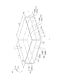
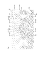
- FIG. 1 is a schematic perspective view of a semiconductor device according to the first embodiment of the present invention.
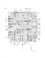
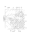
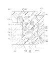
- FIG. 2 is a plan view showing the structure on the first main surface of the semiconductor layer shown in FIG. 1 through the sealing resin layer.
- FIG. 3 is an enlarged view of the region III shown in FIG.
- FIG. 4 is an enlarged view of the area IV shown in FIG.
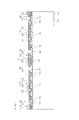
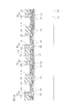
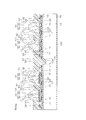
- FIG. 5 is a schematic cross-sectional view of the semiconductor device shown in FIG.
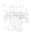
- FIG. 6 is an enlarged view of area VI in FIG.
- FIG. 7 is an enlarged view of the area VII of FIG.
- FIG. 8 is an enlarged view of the area VIII in FIG. 7.
- FIG. 9 is an enlarged view of the area IX in FIG. FIG.
- 10A is a sectional view for explaining the example of the method for manufacturing the semiconductor device shown in FIG. 1.
- 10B is a cross-sectional view showing a step after FIG. 10A.
- FIG. 10C is a cross-sectional view showing a step after FIG. 10B.
- 10D is a cross-sectional view showing a step after FIG. 10C.
- 10E is a cross-sectional view showing a step after FIG. 10D.
- 10F is a cross-sectional view showing a step after FIG. 10E.
- FIG. 10G is a sectional view showing a step after FIG. 10F.
- 10H is a cross-sectional view showing a step after FIG. 10G.
- 10I is a cross-sectional view showing a step after FIG. 10H.
- 10J is a cross-sectional view showing a step after FIG. 10I.
- FIG. 10K is a sectional view showing a step after FIG. 10J.
- 10L is a cross-sectional view showing a step after FIG. 10K.
- 10M is a cross-sectional view showing a step after FIG. 10L.
- 10N is a cross-sectional view showing a step after FIG. 10M.
- 10O is a sectional view showing a step after FIG. 10N.
- 10P is a cross-sectional view showing a step after FIG. 10O.
- 10Q is a cross-sectional view showing a step after FIG. 10P.
- 10R is a cross-sectional view showing a step after FIG. 10Q.
- FIG. 10I is a cross-sectional view showing a step after FIG. 10I.
- FIG. 10K is a sectional view showing a step after FIG. 10J.
- 10L is a cross-sectional view showing
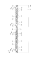
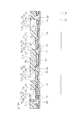
- FIG. 11 is a cross-sectional view corresponding to FIG. 5, and is a schematic cross-sectional view of the semiconductor device according to the second embodiment of the present invention.
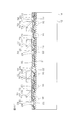
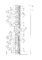
- FIG. 12 is a cross-sectional view corresponding to FIG. 5, and is a schematic cross-sectional view of the semiconductor device according to the third embodiment of the present invention.
- FIG. 13 is an enlarged view of the area XIII in FIG.
- FIG. 14 is an enlarged view of the area XIV in FIG.
- FIG. 1 is a schematic perspective view of a semiconductor device 1 according to the first embodiment of the present invention.
- FIG. 2 is a plan view showing the structure on the first main surface 13 of the semiconductor layer 12 shown in FIG. 1 through the sealing resin layer 93.
- FIG. 3 is an enlarged view of the region III shown in FIG.
- FIG. 4 is an enlarged view of the area IV shown in FIG.
- FIG. 5 is a schematic cross-sectional view of the semiconductor device 1 shown in FIG.
- FIG. 6 is an enlarged view of area VI in FIG.
- FIG. 7 is an enlarged view of the area VII of FIG.
- FIG. 8 is an enlarged view of the area VIII in FIG. 7.
- FIG. 9 is an enlarged view of the area IX in FIG.
- FIG. 5 schematically shows a configuration necessary for the description, and does not show a cross section of a specific portion of the semiconductor device 1.
- the semiconductor device 1 is an electronic component to which a WL-CSP (Wafer Level-Chip Size Package) is applied as a package type.
- the semiconductor device 1 includes a device body 2 formed in a rectangular parallelepiped shape.
- the device body 2 includes a first device main surface 3 on one side, a second device main surface 4 on the other side, and device side surfaces 5A, 5B, 5C connecting the first device main surface 3 and the second device main surface 4. , 5D.
- the first device main surface 3 and the second device main surface 4 are formed in a quadrangular shape (square shape in this embodiment) in a plan view (hereinafter, simply referred to as “plan view”) viewed from the normal direction Z thereof. ing.
- the first device main surface 3 is formed as a mounting surface that faces the mounting board when mounted on a connection target such as the mounting board.
- the device side surfaces 5A to 5D extend in a plane along the normal direction Z.
- the device side surface 5A and the device side surface 5C extend in the first direction X and face each other in the second direction Y intersecting the first direction X.
- the device side surface 5B and the device side surface 5D extend along the second direction Y and face each other in the first direction X.
- the second direction Y is more specifically orthogonal to the first direction X.
- the length L1 of the device side surface 5A and the device side surface 5C may be 0.1 mm or more and 10 mm or less.
- the length L1 may be 0.1 mm or more and 2 mm or less, 2 mm or more and 4 mm or less, 4 mm or more and 6 mm or less, 6 mm or more and 8 mm or less, or 8 mm or more and 10 mm or less.
- the length L2 of the device side surface 5B and the device side surface 5D may be 0.1 mm or more and 10 mm or less.
- the length L1 may be 0.1 mm or more and 2 mm or less, 2 mm or more and 4 mm or less, 4 mm or more and 6 mm or less, 6 mm or more and 8 mm or less, or 8 mm or more and 10 mm or less.
- the thickness T of the device body 2 may be 100 ⁇ m or more and 1500 ⁇ m or less.
- the thickness T may be 100 ⁇ m or more and 250 ⁇ m or less, 250 ⁇ m or more and 500 ⁇ m or less, 500 ⁇ m or more and 750 ⁇ m or less, 750 ⁇ m or more and 1000 ⁇ m or less, 1000 ⁇ m or more and 1250 ⁇ m or less, or 1250 ⁇ m or more and 1500 ⁇ m or less.
- the device body 2 includes a semiconductor layer 12.
- the semiconductor layer 12 is formed in a rectangular parallelepiped shape.
- the semiconductor layer 12 may be a Si semiconductor layer containing Si (silicon).
- the Si semiconductor layer may have a laminated structure including a Si semiconductor substrate and a Si epitaxial layer.
- the Si semiconductor layer may have a single layer structure composed of a Si semiconductor substrate.
- the semiconductor layer 12 may be a wide band gap semiconductor layer containing a wide band gap semiconductor material having a band gap of 2.0 eV or more.
- the semiconductor layer 12 may be a SiC semiconductor layer containing SiC (silicon carbide) as an example of a wide band gap semiconductor material.
- the SiC semiconductor layer may have a laminated structure including a SiC semiconductor substrate and a SiC epitaxial layer.
- the SiC semiconductor layer may have a single layer structure made of a SiC semiconductor substrate.
- the semiconductor layer 12 may be a compound semiconductor layer containing a compound semiconductor material.
- the compound semiconductor layer may have a laminated structure including a compound semiconductor substrate and a compound semiconductor epitaxial layer.
- the compound semiconductor layer may have a single layer structure composed of a compound semiconductor substrate.
- the compound semiconductor material may be a III-V group compound semiconductor material.
- the III-V compound semiconductor material may include at least one of AlN (aluminum nitride), InN (indium nitride), GaN (gallium nitride), and GaAs (gallium arsenide).
- the semiconductor layer 12 includes a first main surface 13 on one side, a second main surface 14 on the other side, and side surfaces 15A, 15B, 15C, 15D connecting the first main surface 13 and the second main surface 14.
- the side surfaces 15A to 15D form part of the device side surfaces 5A to 5D, respectively.
- the side surfaces 15A to 15D are grinding surfaces in this embodiment.
- the thickness of the semiconductor layer 12 may be 50 ⁇ m or more and 1000 ⁇ m or less.
- the thickness of the semiconductor layer 12 may be 50 ⁇ m or more and 200 ⁇ m or less, 200 ⁇ m or more and 400 ⁇ m or less, 400 ⁇ m or more and 600 ⁇ m or less, 600 ⁇ m or more and 800 ⁇ m or less, or 800 ⁇ m or more and 1000 ⁇ m or less.
- the first main surface 13 is formed as a device formation surface on which the main structure of the functional device 16 is formed.
- the functional device 16 is formed by utilizing the surface layer portion of the first main surface 13 of the semiconductor layer 12 and / or the region on the first main surface 13 of the semiconductor layer 12. In FIG. 5, the functional device 16 is simplified by the broken line shown in the surface layer portion of the first main surface 13 of the semiconductor layer 12.
- the functional device 16 may include at least one of a passive device, a semiconductor rectifying device, and a semiconductor switching device.
- Passive devices may include semiconductor passive devices.
- the passive device semiconductor passive device
- the passive device may include at least one of a resistor, a capacitor, and a coil.
- the semiconductor rectifying device may include at least one of a pn junction diode, a Zener diode, a Schottky barrier diode, and a fast recovery diode.
- the semiconductor switching device includes at least one of BJT (Bipolar Junction Transistor), MISFET (Metal Insulator Field Effect Transistor), IGBT (Insulated Gate Bipolar Junction Transistor), and JFET (Junction Field Effect Transistor). Good.
- BJT Bipolar Junction Transistor
- MISFET Metal Insulator Field Effect Transistor
- IGBT Insulated Gate Bipolar Junction Transistor
- JFET Joint Field Effect Transistor
- the functional device 16 may include a circuit network in which any two or more devices selected from passive devices (semiconductor passive devices), semiconductor rectifying devices, and semiconductor switching devices are selectively combined.
- the circuitry may form part or all of an integrated circuit.
- the integrated circuit may include SSI (Small Scale Integration), LSI (Large Scale Integration), MSI (Medium Scale Integration), VLSI (Very Large Scale Integration), or ULSI (Ultra-Very Large Scale Integration).
- the device body 2 includes a main surface insulating layer 21.
- the main surface insulating layer 21 covers the first main surface 13 of the semiconductor layer 12.
- the principal surface insulating layer 21 may have a single layer structure composed of a single insulating layer.
- the main surface insulating layer 21 may have a laminated structure in which a plurality of insulating layers are laminated.
- the single or multiple insulating layers applied as the main surface insulating layer 21 may include a silicon oxide layer and / or a silicon nitride layer.
- the main surface insulating layer 21 may have a multilayer wiring structure.
- the multilayer wiring structure may include a plurality of insulating layers and one or a plurality of wiring layers selectively interposed in a region between the plurality of insulating layers.
- the plurality of wiring layers are electrically connected to the functional device 16.
- the device body 2 includes a plurality of wiring electrodes 22 formed on the main surface insulating layer 21. Each of the plurality of wiring electrodes 22 is selectively routed on the main surface insulating layer 21. The plurality of wiring electrodes 22 are electrically connected to the functional device 16. The plurality of wiring electrodes 22 may include one or more electrically opened wiring electrodes 22.
- the planar shape of the plurality of wiring electrodes 22 is arbitrary and is not limited to a particular shape.
- the wiring electrode 22 may include at least one of aluminum, copper, an aluminum alloy, and a copper alloy.
- the wiring electrode 22 may include at least one of an Al-Si-Cu (aluminum-silicon-copper) alloy, an Al-Si (aluminum-silicon) alloy, and an Al-Cu (aluminum-copper) alloy. Good.
- the wiring electrode 22 preferably contains aluminum.
- the device body 2 includes a protective insulating layer 23.
- the protective insulating layer 23 collectively covers the plurality of wiring electrodes 22 on the main surface insulating layer 21.
- the protective insulating layer 23 protects the underlying structure including the plurality of wiring electrodes 22.
- the protective insulating layer 23 is also called a passivation layer.
- the protective insulating layer 23 may have a single layer structure composed of a single insulating layer.
- the protective insulating layer 23 may have a laminated structure in which a plurality of insulating layers are laminated.
- the single or multiple insulating layers applied as protective insulating layer 23 may include silicon oxide layers and / or silicon nitride layers. In this form, the protective insulating layer 23 has a single-layer structure made of a silicon nitride layer.
- the protective insulating layer 23 has a plurality of first pad openings 25.
- the plurality of first pad openings 25 expose part of regions of the plurality of wiring electrodes 22 as electrode pads 24, respectively.
- the planar shape of each first pad opening 25 is arbitrary and is not limited to a specific shape.
- Each first pad opening 25 may be formed in a polygonal shape such as a triangular shape, a quadrangular shape, a hexagonal shape, or the like in a plan view, or may be formed in a circular shape or an elliptical shape.
- the plurality of electrode pads 24 may be regularly arranged or may be irregularly arranged.
- the plurality of electrode pads 24 may form a plurality of groups according to their arrangement.
- FIG. 2 shows a form in which the plurality of electrode pads 24 include a first electrode pad group 26, a second electrode pad group 27, and a third electrode pad group 28.
- the first electrode pad group 26 includes a plurality of electrode pads 24 arranged in a row at equal intervals along the first direction X or the second direction Y.
- the second electrode pad group 27 is arranged in a row at equal intervals along the first direction X, and is arranged in a row at equal intervals along the second direction Y. It includes a plurality of electrode pads 24.
- the third electrode pad group 28 includes a plurality of electrode pads 24 that are irregularly arranged at different intervals.
- the device body 2 includes a rewiring structure 31.
- the rewiring structure 31 covers the plurality of wiring electrodes 22 on the main surface insulating layer 21.
- the redistribution structure 31 includes a base layer 32 and a plurality of redistribution layers 33 (redistribution).
- the base layer 32 covers the plurality of wiring electrodes 22 on the protective insulating layer 23.
- the base layer 32 has a plurality of second pad openings 35.
- the plurality of second pad openings 35 respectively expose the corresponding electrode pads 24. More specifically, the plurality of second pad openings 35 expose the corresponding electrode pads 24 in a one-to-one correspondence relationship.
- each second pad opening 35 is arbitrary and is not limited to a specific shape.
- Each second pad opening 35 may be formed in a polygonal shape such as a triangular shape, a quadrangular shape, or a hexagonal shape in a plan view, or may be formed in a circular shape or an elliptical shape.
- Each second pad opening 35 includes an inner wall located in a region surrounded by the inner wall of each first pad opening 25 in this embodiment. That is, in this embodiment, the base layer 32 enters each first pad opening 25 from above the protective insulating layer 23 to expose each electrode pad 24. The base layer 32 covers the inner wall of each first pad opening 25 and a part of each electrode pad 24 in each first pad opening 25.
- each second pad opening 35 may communicate with the inner wall of each first pad opening 25.
- the inner wall of each second pad opening 35 may be formed flush with the inner wall of each first pad opening 25, or may be formed outside the inner wall of each first pad opening 25. ..
- the base layer 32 includes an organic insulating material.
- the base layer 32 contains a photosensitive resin as an example of an organic insulating material.
- the base layer 32 may include a polyimide resin as an example of a negative type photosensitive resin.
- the base layer 32 may include polybenzoxazole as an example of a positive type photosensitive resin.
- the thickness of the base layer 32 may be 1 ⁇ m or more and 20 ⁇ m.
- the thickness of the underlayer 32 may be 1 ⁇ m or more and 5 ⁇ m or less, 5 ⁇ m or more and 10 ⁇ m or less, 10 ⁇ m or more and 15 ⁇ m or less, or 15 ⁇ m or more and 20 ⁇ m or less.
- Each rewiring layer 33 is connected to the corresponding electrode pad 24.
- Each redistribution layer 33 is drawn out from the corresponding electrode pad 24 onto the base layer 32. Most of each redistribution layer 33 is located in a region outside the corresponding electrode pad 24.
- each rewiring layer 33 has a pad connecting portion 36, an electrode connecting portion 37, and a wiring portion 38.
- the pad connecting portion 36 covers the electrode pad 24 and is electrically connected to the electrode pad 24 in the second pad opening 35.
- the planar shape of the pad connecting portion 36 is arbitrary and is not limited to a specific shape.
- the electrode connecting portion 37 is formed on the base layer 32 with a space from the pad connecting portion 36.
- the electrode connecting portion 37 has a plane area that exceeds the plane area of the electrode pad 24.
- the planar shape of the electrode connecting portion 37 is arbitrary and is not limited to a specific shape.
- the wiring portion 38 connects the pad connecting portion 36 and the electrode connecting portion 37.
- the wiring portion 38 extends in a region between the pad connecting portion 36 and the electrode connecting portion 37.
- the planar shape of the wiring portion 38 is arbitrary and is not limited to a specific shape.
- the plurality of rewiring layers 33 may have a plurality of types of names depending on the connection mode with the electrode pads 24.
- the plurality of redistribution layers 33 may include a first redistribution layer 33A and a second redistribution layer 33B.
- the first redistribution layer 33A is connected to only one electrode pad 24.
- the second redistribution layer 33B is connected to the plurality of electrode pads 24.
- the first redistribution layer 33A includes a first pad connecting portion 36A, a first electrode connecting portion 37A, and a first wiring portion 38A.
- the first pad connecting portion 36A covers the corresponding one electrode pad 24 and is electrically connected to the electrode pad 24 in the second pad opening 35.
- the planar shape of the first pad connecting portion 36A is arbitrary and is not limited to a specific shape.
- the first pad connecting portion 36A may be formed in a polygonal shape such as a triangular shape, a quadrangular shape, or a hexagonal shape in a plan view, or may be formed in a circular shape or an elliptical shape.
- the first electrode connecting portion 37A is formed on the base layer 32 with a space from the first pad connecting portion 36A.
- the first electrode connecting portion 37A has a plane area that exceeds the plane area of one corresponding electrode pad 24.
- the first electrode connecting portion 37A has an arbitrary planar shape and is not limited to a specific shape.
- the first electrode connecting portion 37A may be formed in a polygonal shape such as a triangular shape, a quadrangular shape, or a hexagonal shape in a plan view, or may be formed in a circular shape or an elliptical shape.
- the first wiring portion 38A connects the first pad connecting portion 36A and the first electrode connecting portion 37A.
- the first wiring portion 38A extends in a region between the first pad connecting portion 36A and the first electrode connecting portion 37A.
- the planar shape of the first wiring portion 38A is arbitrary and is not limited to a specific shape.
- the first wiring portion 38A may extend in a region between the first pad connecting portion 36A and the first electrode connecting portion 37A in a strip shape, a linear shape, an L shape, or a zigzag shape.
- the first wiring portion 38A may cross the other rewiring layer 33 along the first direction X and / or the second direction Y.
- the first wiring portion 38A may extend so as not to cross the other rewiring layer 33 along the first direction X and / or the second direction Y.
- the first pad connecting portion 36A, the first electrode connecting portion 37A, and the first wiring portion 38A may be formed in a polygonal shape as a whole without distinguishing their respective planar shapes.
- the second rewiring layer 33B has a second pad connecting portion 36B, a second electrode connecting portion 37B, and a second wiring portion 38B.
- the second redistribution layer 33B includes a plurality of (two in this embodiment) second electrode connecting portions 37B and a plurality of (two in this embodiment) second wiring portions 38B in this embodiment.
- the second pad connecting portion 36B collectively covers a plurality of corresponding electrode pads 24.
- the second pad connecting portion 36B is electrically connected to the corresponding electrode pad 24 in the corresponding plurality of second pad openings 35.
- the planar shape of the second pad connecting portion 36B is arbitrary and is not limited to a specific shape.
- the plurality of second electrode connecting portions 37B are formed on the base layer 32 at intervals from the second pad connecting portions 36B.
- Each second electrode connecting portion 37B has a plane area that exceeds the plane area of the electrode pad 24.
- the planar shape of each second electrode connecting portion 37B is arbitrary and is not limited to a specific shape.
- the plurality of second wiring portions 38B respectively connect the second pad connecting portions 36B and the corresponding second electrode connecting portions 37B.
- Each second wiring portion 38B extends in a region between the second pad connecting portion 36B and the corresponding second electrode connecting portion 37B.
- the planar shape of each second wiring portion 38B is arbitrary and is not limited to a specific shape.
- Each second wiring portion 38B may extend in a region between the second pad connecting portion 36B and the corresponding second electrode connecting portion 37B in a strip shape, a linear shape, an L shape, or a zigzag shape.
- Each second wiring portion 38B may cross the other rewiring layer 33 along the first direction X and / or the second direction Y.
- Each second wiring part 38B may extend so as not to cross the other rewiring layer 33 along the first direction X and / or the second direction Y.
- the second pad connecting portion 36B, the second electrode connecting portion 37B, and the second wiring portion 38B may be formed in a polygonal shape as a whole without distinguishing the respective planar shapes.
- each redistribution layer 33 includes a first wiring surface 41 on the semiconductor layer 12 side and a second wiring surface 42 located on the opposite side of the first wiring surface 41.
- the first wiring surface 41 has one or a plurality of contact portions 43 connected to the corresponding one or a plurality of electrode pads 24.
- the second wiring surface 42 is roughened.
- the second wiring surface 42 has a first arithmetic average roughness Ra1.
- the first arithmetic average roughness Ra1 is defined by the following equation (1).
- “L1” in the above formula (1) is an arbitrary length extracted from the roughness curve formed on the second wiring surface 42 along the direction along the average line of the roughness curve.
- the unit of the first arithmetic average roughness Ra1 is “ ⁇ m”.
- the first arithmetic average roughness Ra1 may be 0.5 ⁇ m or more and 2 ⁇ m or less.
- the first arithmetic average roughness Ra1 is 0.5 ⁇ m or more and 0.75 ⁇ m or less, 0.75 ⁇ m or more and 1 ⁇ m or less, 1 ⁇ m or more and 1.25 ⁇ m or less, 1.25 ⁇ m or more and 1.5 ⁇ m or less, 1.5 ⁇ m or more and 1.75 ⁇ m or less, Alternatively, it may be 1.75 ⁇ m or more and 2 ⁇ m or less.
- the first arithmetic average roughness Ra1 is preferably 0.65 ⁇ m or more and 1.3 ⁇ m or less.
- the second wiring surface 42 includes a plurality of wiring recesses 44 and is roughened by the plurality of wiring recesses 44.
- the plurality of wiring recesses 44 are recessed in an irregular shape from the second wiring surface 42 toward the first wiring surface 41. As a result, the irregular wiring structure is formed on the second wiring surface 42.
- the plurality of wiring recesses 44 may include one or more tapered recesses 45.
- the thickened recess 45 has an opening edge 46 and an internal space 47 in which the opening width increases from the opening edge 46 toward the first wiring surface 41.
- the plurality of wiring recesses 44 may include one or more tapered recesses 48.
- the tapered recess 48 has an opening edge 49 and an internal space 50 having an opening width narrowed from the opening edge 49 toward the first wiring surface 41.
- second wiring surface 42 has roughened roughened surface area 51 (first area) and non-roughened surface area 52 (second area) having a surface roughness smaller than that of roughened surface area 51. )including.
- the rough surface region 51 includes a plurality of wiring recesses 44 and has a first arithmetic average roughness Ra1.
- the non-roughened surface area 52 is an area not including the wiring recess 44.
- the non-rough surface area 52 has an arithmetic average roughness of less than the first arithmetic average roughness Ra1 (less than 0.5 ⁇ m).
- the rough surface area 51 is formed on the second wiring surface 42 of the pad connecting portion 36, the electrode connecting portion 37, and the wiring portion 38.
- the non-rough surface region 52 is formed in a region of the second wiring surface 42 of the electrode connecting portion 37, to which a post electrode 70 described later is connected.
- the rough surface area 51 is formed over the entire area other than the non-rough surface area 52.
- each rewiring layer 33 has a laminated structure in which a plurality of wiring layers are laminated in this form.
- Each redistribution layer 33 includes a base wiring layer 55 and a body wiring layer 56 that are stacked in this order from the wiring electrode 22 side.
- the base wiring layer 55 may be referred to as UBM (Under Bump Metal).
- the base wiring layer 55 forms the first wiring surface 41 of the rewiring layer 33.
- the base wiring layer 55 is formed in a film shape along the inner surfaces of the base layer 32 and the second pad openings 35.
- the underlying wiring layer 55 defines a concave space in the second pad opening 35.
- the underlying wiring layer 55 has a laminated structure including a first wiring layer 57 and a second wiring layer 58 which are laminated in this order from the wiring electrode 22 side.
- the second wiring layer 58 contains a conductive material different from that of the first wiring layer 57.
- the first wiring layer 57 includes a Ti layer containing Ti (titanium) as a main component.
- the Ti layer may be a Ti barrier layer.
- the second wiring layer 58 includes a Cu layer containing Cu (copper) as a main component.
- the Cu layer may be a Cu seed layer.
- the body wiring layer 56 forms the second wiring surface 42 of the rewiring layer 33.
- the body wiring layer 56 is formed in a film shape on the base wiring layer 55, following the base wiring layer 55.
- the body wiring layer 56 enters into the concave space defined by the base wiring layer 55 in the second pad opening 35.
- the body wiring layer 56 includes a Cu layer containing Cu (copper) as a main component.
- the body wiring layer 56 has a single layer structure including a Cu layer.
- the Cu layer of the body wiring layer 56 may be a Cu plating layer.
- the body wiring layer 56 may be integrated with the second wiring layer 58.
- the body wiring layer 56 may be formed so that the interface with the second wiring layer 58 disappears.
- the body wiring layer 56 may be formed such that the interface with the second wiring layer 58 remains.
- the first wiring layer 57 has a first peripheral edge 57A.
- the second wiring layer 58 has a second peripheral edge 58A protruding outward from the first peripheral edge 57A.
- the body wiring layer 56 has a third peripheral edge 56A protruding outward from the first peripheral edge 57A.
- the third peripheral edge 56A of the body wiring layer 56 is continuous with the second peripheral edge 58A of the second wiring layer 58. More specifically, the third peripheral edge 56A of the body wiring layer 56 is formed flush with the second peripheral edge 58A of the second wiring layer 58.
- the first peripheral edge 57A, the second peripheral edge 58A, and the third peripheral edge 56A form the peripheral edge of the redistribution layer 33.
- the total thickness of the redistribution layer 33 may be 5 ⁇ m or more and 15 ⁇ m or less.
- the total thickness of the redistribution layer 33 may be 5 ⁇ m or more and 7.5 ⁇ m or less, 7.5 ⁇ m or more and 10 ⁇ m or less, 10 ⁇ m or more and 12.5 ⁇ m or less, or 12.5 ⁇ m or more and 15 ⁇ m or less.
- the underlayer 32 has anchor recesses 61 recessed toward the semiconductor layer 12.
- the anchor recess 61 is formed in a portion of the base layer 32 exposed from the redistribution layer 33.
- the anchor recess 61 includes a bottom wall and a side wall.
- the bottom wall of the anchor recess 61 is located on the first main surface 13 side of the semiconductor layer 12 with respect to the first wiring surface 41 of the redistribution layer 33.
- the bottom wall of the anchor recess 61 may be formed in an uneven shape by rising and / or sinking.
- the sidewall of the anchor recess 61 is located on the inner side of the redistribution layer 33 with respect to the peripheral edge of the redistribution layer 33.
- the bottom wall of the anchor recess 61 includes the exposed portion 62 exposed from the redistribution layer 33 in a plan view and the concealing portion 63 overlapping the redistribution layer 33 in a plan view.
- the concealing portion 63 is formed over the entire periphery of each redistribution layer 33.
- the concealment portion 63 is formed independently of each redistribution layer 33, and has the same contour as the redistribution layer 33 in a plan view.
- Each concealing portion 63 has a curved surface facing the first main surface 13 of the semiconductor layer 12.
- the anchor recess 61 is formed in the entire region of the underlying layer 32 exposed from the redistribution layer 33, and extends between the redistribution layers 33 adjacent to each other. Therefore, the concealing portion 63 of the rewiring layer 33 on one side (for example, the rewiring layer 33 on the left side of FIG. 5) and the rewiring layer 33 on the other side (for example, the rewiring layer 33 on the right side of FIG. 5) are included.
- the concealing portion 63 is continuous through the common exposing portion 62.
- the depth of the anchor recess 61 may be more than 0 ⁇ m and 10 ⁇ m or less.
- the depth of the anchor recess 61 may be more than 0 ⁇ m and 2 ⁇ m or less, 2 ⁇ m or more and 4 ⁇ m or less, 4 ⁇ m or more and 6 ⁇ m or less, 6 ⁇ m or more and 8 ⁇ m or less, or 8 ⁇ m or more and 10 ⁇ m or less.
- the depth of the anchor recess 61 is preferably 1 ⁇ m or more and 5 ⁇ m or less.
- the device body 2 includes a plurality of post electrodes 70.
- the plurality of post electrodes 70 are formed at intervals along the first direction X and the second direction Y in a plan view.
- the plurality of post electrodes 70 are arranged in a matrix in a plan view.
- the plurality of post electrodes 70 are connected to the corresponding electrode connection portions 37 of the rewiring layer 33. More specifically, the plurality of post electrodes 70 are connected to the non-rough surface region 52 at the electrode connection portion 37 of the corresponding redistribution layer 33. One post electrode 70 is connected to one electrode connection portion 37 of the first redistribution layer 33A. One post electrode 70 is connected to each of the two electrode connecting portions 37 of the second redistribution layer 33B.
- the plurality of post electrodes 70 are each formed in a columnar shape extending along the normal line direction (normal line direction Z) of the second wiring surface 42 of the rewiring layer 33.
- the post electrode 70 is also called a pillar electrode.
- the plurality of post electrodes 70 may be formed in a polygonal columnar shape such as a square columnar shape, a hexagonal columnar shape, or a cylindrical shape or an elliptic cylindrical shape.
- the plurality of post electrodes 70 are formed in a cylindrical shape in this form.
- the plurality of post electrodes 70 include a first electrode surface 71 connected to the second wiring surface 42 in the corresponding rewiring layer 33, a second electrode surface 72 located on the opposite side of the first electrode surface 71, and a first electrode surface 71. It has the electrode side surface 73 which connects the electrode surface 71 and the 2nd electrode surface 72, respectively.
- the second electrode surface 72 has a flat surface.
- the second electrode surface 72 is formed parallel to the first main surface 13 of the semiconductor layer 12. More specifically, the second electrode surface 72 is a ground surface.
- the second electrode surface 72 functions as a mounting terminal. That is, the semiconductor device 1 is mounted on a connection target such as a mounting board by bonding the second electrode surface 72 to the connection target.
- the electrode side surface 73 extends in a plane along the normal direction Z.
- the plurality of post electrodes 70 may include one or a plurality of tapered post electrodes 70 formed in a tapered shape from the second electrode surface 72 toward the first electrode surface 71.
- the tapered post electrode 70 includes the first electrode surface 71 having the first plane area, the second electrode surface 72 having the second plane area exceeding the first plane area, and the first to second electrode surfaces 71 to 71. It has an electrode side surface 73 that is inclined downward toward the electrode surface 72.
- the tapered post electrode 70 may be formed asymmetrically (more specifically, a non-symmetrical shape) with respect to the normal line of the first electrode surface 71 in a cross-sectional view. That is, the tapered post electrode 70 may be formed such that the inclination angle of the electrode side surface 73 on one side is different from the inclination angle of the electrode side surface 73 on the other side in cross-sectional view. Of course, all post electrodes 70 may be tapered.
- the post electrode 70 has a thickness exceeding the thickness of the rewiring layer 33.
- the ratio of the thickness of the post electrode 70 to the thickness of the redistribution layer 33 may be more than 1 and 30 or less.
- the ratio of the thickness of the post electrode 70 to the thickness of the redistribution layer 33 is more than 1 and 5 or less, 5 or more and 10 or less, 10 or more and 15 or less, 15 or more and 20 or less, 20 or more and 25 or less, or 25 or more and 30 or more. It may be the following.
- the thickness of the post electrode 70 may be 50 ⁇ m or more and 150 ⁇ m or less.
- the thickness of the post electrode 70 may be 50 ⁇ m or more and 75 ⁇ m or less, 75 ⁇ m or more and 100 ⁇ m or less, 100 ⁇ m or more and 125 ⁇ m or less, or 125 ⁇ m or more and 150 ⁇ m or less.
- the thickness of the post electrode 70 is preferably 90 ⁇ m or more and 110 ⁇ m or less.
- the electrode side surface 73 is roughened.
- the electrode side surface 73 has a second arithmetic average roughness Ra2.
- the second arithmetic average roughness Ra2 is defined by the following equation (2).
- “L2” in the above equation (2) is an arbitrary length extracted from the roughness curve formed on the electrode side surface 73 along the direction along the average line of the roughness curve.
- the unit of the second arithmetic average roughness Ra2 is “ ⁇ m”.
- the second arithmetic average roughness Ra2 of the electrode side surface 73 is less than the first arithmetic average roughness Ra1 of the second wiring surface 42 (Ra1> Ra2).
- the second arithmetic average roughness Ra2 may be more than 0 ⁇ m and less than 0.5 ⁇ m.
- the second arithmetic average roughness Ra2 exceeds 0 ⁇ m and is 0.1 ⁇ m or less, 0.1 ⁇ m or more and 0.2 ⁇ m or less, 0.2 ⁇ m or more and 0.3 ⁇ m or less, 0.3 ⁇ m or more and 0.4 ⁇ m or less, or 0.4 ⁇ m. It may be 0.5 ⁇ m or less.
- the second arithmetic average roughness Ra2 is preferably 0.1 ⁇ m or more and 0.3 ⁇ m or less.
- the electrode side surface 73 includes a plurality of electrode recesses 74, and is roughened by the plurality of electrode recesses 74.
- the plurality of electrode recesses 74 are recessed in an irregular shape from the electrode side surface 73 toward the inside. As a result, an irregular concavo-convex structure is formed on the electrode side surface 73.
- the plurality of electrode recesses 74 may include one or more tapered recesses 75.
- the thickened recess 75 has an opening edge 76 and an internal space 77 in which the opening width expands inward from the opening edge 76.
- the plurality of electrode recesses 74 may include one or more tapered recesses 78.
- the tapered recess 78 has an opening edge 79 and an internal space 80 in which the opening width narrows inward from the opening edge 79.
- the electrode side surface 73 may include a wiring / electrode recess 81 that is integral with the wiring recess 44 at the connection portion with the second wiring surface 42. From the wiring / electrode recess 81, the rewiring layer 33 and the post electrode 70 are exposed.
- the wiring / electrode recess 81 includes an opening edge 82 and an internal space 83.
- the wiring / electrode recess 81 may have an internal space 83 extending from the opening edge 82 along the lateral direction parallel to the second wiring surface 42.
- the wiring / electrode recess 81 may be a thickened recess having an internal space 83 whose opening width expands inward from the opening edge 82.
- the wiring / electrode recess 81 may be a tapered recess having an internal space 83 whose opening width narrows inward from the opening edge 82.
- the device body 2 includes a sealing resin layer 93 (resin).
- the sealing resin layer 93 forms the first device main surface 3.
- the encapsulating resin layer 93 includes the plurality of redistribution layers 33 and the plurality of post electrodes 70 on the first main surface 13 of the semiconductor layer 12 so as to expose the second electrode surfaces 72 of the plurality of post electrodes 70. It covers all at once.
- the sealing resin layer 93 includes a resin main surface 94 and resin side surfaces 95A, 95B, 95C, 95D.
- the resin main surface 94 is continuous with the second electrode surface 72 of the plurality of post electrodes 70.
- the resin main surface 94 is formed flush with the second electrode surface 72 of the plurality of post electrodes 70. More specifically, the resin main surface 94 forms one ground surface with the second electrode surfaces 72 of the plurality of post electrodes 70.
- the resin side surfaces 95A to 95D extend from the peripheral edge of the resin main surface 94 toward the semiconductor layer 12, and are connected to the side surfaces 15A to 15D.
- the resin side surfaces 95A to 95D are continuous with the side surfaces 15A to 15D. More specifically, the resin side surfaces 95A to 95D are formed flush with the side surfaces 15A to 15D.
- the resin side surfaces 95A to 95D form one grinding surface with the side surfaces 15A to 15D.
- the thickness of the sealing resin layer 93 may be 50 ⁇ m or more and 200 ⁇ m or less.
- the thickness of the sealing resin layer 93 may be 50 ⁇ m or more and 75 ⁇ m or less, 75 ⁇ m or more and 100 ⁇ m or less, 100 ⁇ m or more and 125 ⁇ m or less, 125 ⁇ m or more and 150 ⁇ m or less, 150 ⁇ m or more and 175 ⁇ m or less, or 175 ⁇ m or more and 200 ⁇ m or less.
- the thickness of the sealing resin layer 93 is preferably 100 ⁇ m or more and 120 ⁇ m or less.
- the portion of the sealing resin layer 93 that covers the second wiring surface 42 of the rewiring layer 33 enters the plurality of wiring recesses 44.
- the adhesion of the sealing resin layer 93 to the plurality of rewiring layers 33 is enhanced.
- the portion of the sealing resin layer 93 that covers the electrode side surface 73 of the post electrode 70 enters into the plurality of electrode recesses 74 (wiring / electrode recesses 81).
- the adhesion of the sealing resin layer 93 to the plurality of post electrodes 70 is increased.
- the portion of the sealing resin layer 93 that covers the base layer 32 is in the anchor recess 61.
- the adhesion of the sealing resin layer 93 to the base layer 32 is enhanced.
- a portion of the sealing resin layer 93 located inside the anchor recess 61 fills the exposed portion 62 and the concealing portion 63 of the anchor recess 61.
- the adhesion of the sealing resin layer 93 to the base layer 32 is enhanced.
- a part of the sealing resin layer 93 located inside the anchor recess 61 meshes with a part defined by the anchor recess 61 and the rewiring layer 33. Further, the sealing resin layer 93 sandwiches the first wiring surface 41 and the second wiring surface 42 of the rewiring layer 33 from the inside and the outside of the anchor recess 61. Thereby, the adhesive force of the sealing resin layer 93 to the base layer 32 is appropriately increased.
- sealing resin layer 93 includes a thermosetting resin as an example of a mold resin.
- the thermosetting resin may include an epoxy resin.
- the sealing resin layer 93 includes a matrix resin 96 and a plurality of fillers 97 added (filled) to the matrix resin 96.
- the matrix resin 96 includes an epoxy resin in this form.
- the plurality of fillers 97 include silicon oxide and are formed into particles or spheres each having a non-uniform diameter (size).
- the plurality of fillers 97 include a plurality of large diameter fillers 98 and a plurality of small diameter fillers 99.
- the plurality of large-diameter fillers 98 include a plurality of fillers 97 having a diameter exceeding the opening width of the wiring recess 44 and the opening width of the electrode recess 74.
- the plurality of small-diameter fillers 99 include a plurality of fillers 97 having a diameter smaller than the opening width of the wiring recess 44 and the opening width of the electrode recess 74.
- the diameter of the plurality of large-diameter fillers 98 may be more than 5 ⁇ m and 15 ⁇ m or less.
- the diameter of the plurality of large-diameter fillers 98 may be more than 5 ⁇ m and 7.5 ⁇ m or less, 7.5 ⁇ m or more and 10 ⁇ m or less, 10 ⁇ m or more and 12.5 ⁇ m or less, or 12.5 ⁇ m or more and 15 ⁇ m or less.
- the diameter of the plurality of small-diameter fillers 99 may be more than 0 ⁇ m and 5 ⁇ m or less.
- the diameters of the plurality of small-diameter fillers 99 are more than 0 ⁇ m and 0.1 ⁇ m or less, 0.1 ⁇ m or more and 0.5 ⁇ m or less, 0.5 ⁇ m or more and 1 ⁇ m or less, 1 ⁇ m or more and 1.5 ⁇ m or less, 1.5 ⁇ m or more and 2 ⁇ m or less, 2 ⁇ m or more.
- It may be 2.5 ⁇ m or less, 2.5 ⁇ m or more and 3 ⁇ m or less, 3 ⁇ m or more and 3.5 ⁇ m or less, 3.5 ⁇ m or more and 4 ⁇ m or less, 4 ⁇ m or more and 4.5 ⁇ m or less, or 4.5 ⁇ m or more and 5 ⁇ m or less.
- the plurality of large-diameter fillers 98 seal the rewiring layer 33 and the post electrode 70 together with the matrix resin 96 in the regions outside the plurality of wiring recesses 44 and the plurality of electrode recesses 74.
- the plurality of small diameter fillers 99 enter the plurality of wiring recesses 44 and the plurality of electrode recesses 74.
- the plurality of small-diameter fillers 99 having a diameter of 1 ⁇ m or less among the plurality of small-diameter fillers 99 easily enter the plurality of wiring recesses 44 and the plurality of electrode recesses 74.
- the plurality of small diameter fillers 99 fill the plurality of wiring recesses 44 and the plurality of electrode recesses 74 together with the matrix resin 96.
- the plurality of small diameter fillers 99 guide the matrix resin 96 into the plurality of wiring recesses 44 and the plurality of electrode recesses 74. In this way, the adhesion of the sealing resin layer 93 to the plurality of redistribution layers 33 and the plurality of post electrodes 70 is enhanced.
- the plurality of small-diameter fillers 99 also enter the tapered recess 45 of the wiring recess 44 and the tapered recess 75 of the electrode recess 74.
- the plurality of small-diameter fillers 99 fill the thickened recesses 45 and the thickened recesses 75 together with the matrix resin 96.
- the plurality of small-diameter fillers 99 have entered the anchor recess 61.
- the plurality of small-diameter fillers 99 fill the anchor recess 61 together with the matrix resin 96.
- the plurality of large-diameter fillers 98 may enter the anchor recess 61.
- the plurality of large-diameter fillers 98 may fill the anchor recess 61 together with the matrix resin 96.
- the sealing resin layer 93 may include bubbles (not shown) having a diameter of more than 0 ⁇ m and not more than 2 ⁇ m.
- the sealing resin layer 93 having such bubbles is formed by the compression molding method.
- the diameters of the bubbles are more than 0 ⁇ m and 0.25 ⁇ m or less, 0.25 ⁇ m or more and 0.5 ⁇ m or less, 0.5 ⁇ m or more and 0.75 ⁇ m or less, 0.75 ⁇ m or more and 1 ⁇ m or less, 1.25 ⁇ m or more and 1.5 ⁇ m or less, 1. It may be 5 ⁇ m or more and 1.75 ⁇ m or less, or 1.75 ⁇ m or more and 2 ⁇ m or less.
- the diameter of the bubbles is preferably 1 ⁇ m or less.
- Bubbles may serve as a starting point of peeling of the sealing resin layer 93. Therefore, by limiting the diameter of the bubbles to 2 ⁇ m or less (preferably 1 ⁇ m or less), the peeling of the sealing resin layer 93 originating from the bubbles can be suppressed.
- the contact area of the sealing resin layer 93 with the rewiring layer 33 can be increased by limiting the bubble diameter to 2 ⁇ m or less (preferably 1 ⁇ m or less). The peeling of the sealing resin layer 93 from the rewiring layer 33 can be appropriately suppressed.
- the contact area of the sealing resin layer 93 with the post electrode 70 can be increased.
- the peeling of the sealing resin layer 93 from the electrode 70 can be appropriately suppressed.
- the anchor recess 61 is formed and the diameter of the bubbles is limited to 2 ⁇ m or less (preferably 1 ⁇ m or less), the contact area of the sealing resin layer 93 with the base layer 32 can be increased. The peeling of the sealing resin layer 93 from the ground layer 32 can be appropriately suppressed.
- the sealing resin layer 93 containing the large-diameter filler 98 and the small-diameter filler 99 in these structures the separation of the sealing resin layer 93 from the anchor recess 61, the rewiring layer 33, and the post electrode 70 is appropriately performed. Can be suppressed.
- the device body 2 includes a main surface protective layer 100.
- the main surface protection layer 100 is formed on the second main surface 14 of the semiconductor layer 12.
- the main surface protective layer 100 may cover the entire surface of the second main surface 14 of the semiconductor layer 12, or may expose a part of the second main surface 14 (for example, the peripheral portion of the second main surface 14). Good.
- the main surface protection layer 100 forms the second device main surface 4 and part of the device side surfaces 5A to 5D.
- the main surface protective layer 100 may have a single layer structure composed of an organic insulating material layer.
- the main surface protection layer 100 may include a thermosetting resin as an example of an organic insulating material layer.
- the main surface protective layer 100 may include an epoxy resin.
- the thickness of the main surface protective layer 100 may be 5 ⁇ m or more and 100 ⁇ m or less.
- the thickness of the main surface protective layer 100 may be 5 ⁇ m or more and 25 ⁇ m or less, 25 ⁇ m or more and 50 ⁇ m or less, 50 ⁇ m or more and 75 ⁇ m or less, or 75 ⁇ m or more and 100 ⁇ m or less.
- the device body 2 includes a plurality of conductive bonding materials 101.
- the plurality of conductive bonding materials 101 are respectively formed on the second electrode surface 72 of the post electrode 70 exposed from the resin main surface 94.
- the plurality of conductive bonding materials 101 are formed in a one-to-one correspondence with the corresponding second electrode surfaces 72. Therefore, the plurality of conductive bonding materials 101 are formed at intervals along the first direction X and the second direction Y.
- the plurality of conductive bonding materials 101 are arranged in a matrix in a plan view.
- the plurality of conductive bonding materials 101 are each formed in a hemispherical shape protruding from the second electrode surface 72.
- the plurality of conductive bonding materials 101 each include solder or metal paste.
- the solder is preferably lead-free.
- the solder may contain Sn (tin).
- the solder may contain at least one of SnAg alloy, SnSb alloy, SnAgCu alloy, SnZnBi alloy, SnCu alloy, SnCuNi alloy, and SnSbNi alloy.
- the metal paste may contain at least one of aluminum, copper, silver, and gold.
- the semiconductor layer 12 includes a peripheral recess 102 formed on the peripheral edge of the first main surface 13.
- the peripheral recess 102 is recessed from the first main surface 13 toward the second main surface 14. More specifically, the peripheral recess 102 penetrates the underlayer 32, the protective insulating layer 23, and the main surface insulating layer 21, and is formed on the first main surface 13.
- the peripheral recess 102 extends in a band shape along the peripheral edge of the first main surface 13 in a plan view. More specifically, the peripheral edge recess 102 is formed in an annular shape (square annular shape in this embodiment) extending along the peripheral edge of the first main surface 13 in a plan view.
- the peripheral recess 102 has a first wall surface 103 located on the first main surface 13 side and a second wall surface 104 located on the second main surface 14 side.
- the first wall surface 103 is inclined with respect to the first main surface 13.
- the second wall surface 104 is inclined with respect to the first wall surface 103.
- the second wall surface 104 is inclined at an angle different from that of the first wall surface 103.
- the recess angle formed by the second wall surface 104 with the first wall surface 103 in the peripheral recess 102 may be more than 90 ° and not more than 150 °.
- the recess angle is more than 90 ° and 100 ° or less, 100 ° or more and 110 ° or less, 110 ° or more and 120 ° or less, 120 ° or more and 130 ° or less, 130 ° or more and 140 ° or less, or 140 ° or more and 150 ° or less. It may be.
- the sealing resin layer 93 has entered the peripheral recess 102.
- the resin side surfaces 95A to 95D are formed by the portion of the sealing resin layer 93 that has entered the peripheral recess 102.
- the plurality of small diameter fillers 99 may enter the peripheral recess 102.
- the plurality of small-diameter fillers 99 may fill the anchor recess 61 together with the matrix resin 96.
- the plurality of large-diameter fillers 98 may enter the anchor recess 61.
- the plurality of large-diameter fillers 98 may fill the anchor recess 61 together with the matrix resin 96.
- FIGS. 10A to 10R are cross-sectional views for explaining an example of a method of manufacturing the semiconductor device 1 shown in FIG.
- the plurality of semiconductor devices 1 are manufactured at the same time, but for convenience, the region where the two semiconductor devices 1 are manufactured is shown.
- a wafer-shaped semiconductor layer 12 is prepared.
- the semiconductor layer 12 may have a thickness of 200 ⁇ m or more and 1000 ⁇ m or less.
- the functional device 16 is formed on the semiconductor layer 12.
- the main surface insulating layer 21 is formed on the first main surface 13.
- the wiring electrode 22 is formed on the main surface insulating layer 21.
- the protective insulating layer 23 is formed on the main surface insulating layer 21.
- the protective insulating layer 23 covers the wiring electrodes 22 on the main surface insulating layer 21.
- a first pad opening 25 exposing a part of the wiring electrode 22 as an electrode pad 24 is formed in the protective insulating layer 23.
- the first pad opening 25 is formed by removing an unnecessary portion of the protective insulating layer 23.
- the unnecessary portion of the protective insulating layer 23 may be removed by an etching method using a mask (not shown).
- the base layer 32 is formed on the protective insulating layer 23.
- the base layer 32 is made of a photosensitive resin in this embodiment.
- the underlayer 32 may be formed by a spin coating method, a spray coating method, or the like.
- the second pad opening 35 exposing the electrode pad 24 is formed in the base layer 32.
- the second pad opening 35 is formed by exposing the underlying layer 32 in a predetermined pattern and then developing it.
- the base wiring layer 55 is formed on the base layer 32.
- a first wiring layer 57 containing Ti (titanium) as a main component and a second wiring layer 58 containing Cu (copper) as a main component are formed in this order from above the base layer 32.
- Including the step of The first wiring layer 57 and the second wiring layer 58 may be respectively formed by a sputtering method.
- a mask 111 having a predetermined pattern is formed on the underlying wiring layer 55.
- the base wiring layer 55 has a plurality of openings 112 that expose a region where the body wiring layer 56 is to be formed.
- body wiring layer 56 containing Cu (copper) as a main component is formed on base wiring layer 55.
- the body wiring layer 56 is formed on a portion of the base wiring layer 55 exposed from the plurality of openings 112.
- the body wiring layer 56 may be formed by a copper plating method.
- the mask 111 is removed.
- a mask 113 is formed on the underlying wiring layer 55 so as to cover the body wiring layer 56.
- the mask 113 may be formed by applying a photosensitive resin.
- the mask 113 may be formed by attaching a mask material such as a dry film made of a photosensitive resin.
- a plurality of openings 114 that respectively expose the regions where the post electrodes 70 are to be formed are formed in the mask 113.
- the plurality of openings 114 are formed by exposing the mask 113 with a predetermined pattern and then developing it.
- the post electrode 70 containing Cu (copper) as a main component is formed on the body wiring layer 56.
- the post electrode 70 is formed on a portion of the body wiring layer 56 exposed from the plurality of openings 114.
- the post electrode 70 may be formed by a copper plating method.
- the mask 113 is removed.
- unnecessary portions of the underlying wiring layer 55 are removed.
- the unnecessary portion of the underlying wiring layer 55 may be removed by an etching method through a mask (not shown).
- the etching method may be a wet etching method.
- the second wiring layer 58 exposed from the body wiring layer 56 is removed.
- the first wiring layer 57 exposed from the second wiring layer 58 is removed.
- the redistribution layer 33 including the base wiring layer 55 and the body wiring layer 56 is formed.
- the groove 115 is formed in the first main surface 13.
- the groove 115 is formed in the first main surface 13 by penetrating the base layer 32, the protective insulating layer 23, and the main surface insulating layer 21.
- the groove 115 serves as a base of the peripheral recess 102.
- the groove 115 may be formed by a grinding method using a grinding member such as a dicing blade.
- the inner wall of the groove 115 is formed in a shape corresponding to the shape of the cutting edge of the grinding member.
- the groove 115 having the first wall surface 103 located on the first main surface 13 side and the second wall surface 104 located on the second main surface 14 side is formed.
- the first wall surface 103 is inclined with respect to the first main surface 13.
- the second wall surface 104 is inclined at an angle different from that of the first wall surface 103.
- the angle (recess angle) formed by the second wall surface 104 with the first wall surface 103 in the groove 115 may be more than 90 ° and 150 ° or less.
- the anchor recess 61 is formed in a portion of the base layer 32 exposed from the rewiring.
- the anchor recess 61 may be formed by an ashing treatment method for the base layer 32. In the ashing method, unnecessary portions of the base layer 32 are isotropically removed. As a result, the anchor recess 61 having the exposed portion 62 and the concealing portion 63 is formed.
- the outer surface of the redistribution layer 33 is roughened, and the outer surface of the post electrode 70 is roughened.
- the step of roughening the redistribution layer 33 and the step of roughening the post electrode 70 are performed simultaneously.
- the outer surface of the redistribution layer 33 and the outer surface of the post electrode 70 are roughened by a wet etching method using a roughening etching liquid that reacts with copper.
- the roughening etching solution may be an aqueous solution containing sulfuric acid and hydrogen peroxide.
- the roughening etching solution may be supplied onto the first main surface 13 of the semiconductor layer 12 in a state where the semiconductor layer 12 is rotated around the rotation axis along the normal direction Z.
- the roughening etching liquid receives the centrifugal force caused by the rotation of the semiconductor layer 12 and is discharged to the outside of the semiconductor layer 12.
- a plurality of wiring recesses 44 are formed on the outer surface of the redistribution layer 33, and a plurality of electrode recesses 74 are formed on the outer surface of the post electrode 70.
- the roughening etching liquid forms a discharge flow path (see an arrow in FIG. 10M) from the central portion of the semiconductor layer 12 toward the peripheral portion in a state where the semiconductor layer 12 is rotated.
- a region of the post electrode 70 located on the upstream side of the discharge flow path on the electrode side surface 73 partially blocks the roughening etching solution.
- the region of the electrode side surface 73 of the post electrode 70 located on the upstream side of the discharge channel may be over-etched.
- the post electrode 70 having a tapered shape in cross section may be formed. More specifically, the post electrode 70 may be formed asymmetrically (more specifically, in a non-axisymmetric shape) with respect to the normal line of the first electrode surface 71 in cross-sectional view.
- Rinsing process may be performed after the roughening process.
- the rinse liquid may be supplied onto the first main surface 13 of the semiconductor layer 12 in a state where the semiconductor layer 12 is rotated around the rotation axis along the normal direction Z.
- the roughening etching liquid remaining on the first main surface 13 is washed away by the rinse liquid.
- the rinse liquid may include at least one of pure water (deionized water), carbonated water, electrolytic ion water, hydrogen water, ozone water, and hydrochloric acid water having a dilute concentration.
- the sealing resin layer 93 is formed on the first main surface 13 of the semiconductor layer 12.
- the sealing resin layer 93 collectively covers the redistribution layer 33 and the post electrode 70.
- the sealing resin layer 93 includes a matrix resin 96 (epoxy resin) and a plurality of fillers 97 added (filled) to the matrix resin 96 and having a non-uniform diameter.
- the plurality of fillers 97 include a plurality of large diameter fillers 98 and a plurality of small diameter fillers 99.
- the sealing resin layer 93 is formed by being pressed and solidified by a compression molding method under a reduced pressure atmosphere.
- the air pressure at the time of forming the sealing resin layer 93 is set so that the diameter of the bubbles in the sealing resin layer 93 is 2 ⁇ m or less (preferably 1 ⁇ m or less).
- the sealing resin layer 93 that fills the wiring recess 44, the electrode recess 74, the anchor recess 61, and the groove 115 and collectively covers the rewiring layer 33 and the post electrode 70 is formed.
- a step of forming an oxidation suppressing film that collectively covers the redistribution layer 33 and the post electrode 70 may be performed prior to the step of forming the sealing resin layer 93.
- the oxidation suppressing film protects the redistribution layer 33 and the post electrode 70 from oxidation.
- the oxidation suppressing film may be an organic thin film containing an organic insulating material.
- the organic thin film may have a thickness of 0.1 nm or more and 10 nm or less.
- the organic thin film may contain an epoxy resin.
- the sealing resin layer 93 is formed integrally with the oxidation suppressing film in the step of forming the sealing resin layer 93. That is, the oxidation suppression film is incorporated as a part of the sealing resin layer 93.
- the sealing resin layer 93 may be formed in such a manner that the interface with the oxidation suppressing film remains.
- the resin main surface 94 of the sealing resin layer 93 is ground until the post electrode 70 is exposed.
- the sealing resin layer 93 may be ground by a CMP (Chemical Mechanical Polishing) method.
- CMP Chemical Mechanical Polishing
- the second electrode surface 72 of the post electrode 70 is ground together with the resin main surface 94 of the sealing resin layer 93.
- the resin main surface 94 of the sealing resin layer 93 forms one ground surface together with the second electrode surface 72 of the post electrode 70.
- the semiconductor layer 12 is thinned to a desired thickness by grinding from the second major surface 14 side.
- the semiconductor layer 12 may be ground by the CMP method.
- the main surface protection layer 100 is formed on the second main surface 14 of the semiconductor layer 12.
- the main surface protective layer 100 contains an epoxy resin.
- the main surface protective layer 100 may be formed by a spin coating method, a spray coating method, or the like.
- the conductive bonding material 101 is formed on the second electrode surface 72 of the post electrode 70.
- the conductive bonding material 101 may include solder.
- the reflow process may be performed at a temperature at which the solder melts.
- the wafer-shaped semiconductor layer 12 is cut along the grooves 115.
- a plurality of semiconductor devices 1 are cut out from one wafer-shaped semiconductor layer 12.
- the semiconductor layer 12 is cut by a grinding member such as a dicing blade.
- a dicing blade having a cutting edge smaller than the width of the groove 115 may be used.
- a portion of the sealing resin layer 93 that covers the groove 115 is a part of the device side surfaces 5A to 5D of the device body 2.
- the semiconductor device 1 is manufactured through the steps including the above.
- the process order of FIGS. 10A to 10R is an example, and the process order is not limited.
- the roughening step (see FIG. 10M) may be performed prior to the groove forming step (see FIG. 10K).
- the roughening step for the redistribution layer 33 and the roughening step for the post electrode 70 (see FIG. 10M) may be performed at different timings.
- the roughening step (see FIG. 10M) for the redistribution layer 33 is performed after the forming step of the body wiring layer 56 (see FIG. 10E) and prior to the forming step of the post electrode 70 (see FIG. 10I). Good. In this case, the entire area of the second wiring surface 42 of the rewiring layer 33 is roughened.
- the roughening step (see FIG. 10M) for the post electrode 70 may be performed at any timing after the step of forming the post electrode 70 (see FIG. 10I).
- the post electrode 70 is formed on the roughened second wiring surface 42 in the redistribution layer 33.
- the post electrode 70 is formed in the non-roughened region (non-roughened region 52) of the second wiring surface 42. Therefore, it is preferable that the surface roughening step for the redistribution layer 33 and the surface roughening step for the post electrodes 70 be performed at the same time.
- the adhesion of the sealing resin layer 93 to the rewiring layer 33 can be increased by the roughened second wiring surface 42. Further, according to the semiconductor device 1, the adhesion force of the sealing resin layer 93 to the post electrode 70 can be enhanced by the roughened electrode side surface 73. Therefore, peeling of the sealing resin layer 93 can be suppressed.
- the post electrode 70 is formed on the non-rough surface region 52 on the second wiring surface 42 of the rewiring layer 33.
- the adhesiveness of the sealing resin layer 93 can be increased while improving the film forming property of the post electrode 70 on the redistribution layer 33.
- the sealing resin layer 93 includes the matrix resin 96 and the plurality of fillers 97 each having a non-uniform diameter.
- the plurality of large-diameter fillers 98 of the plurality of fillers 97 seal the redistribution layer 33 and the post electrode 70 together with the matrix resin 96 in the regions outside the plurality of wiring recesses 44 and the plurality of electrode recesses 74.
- the plurality of small diameter fillers 99 among the plurality of fillers 97 fill the plurality of wiring recesses 44 and the plurality of electrode recesses 74 together with the matrix resin 96.
- the adhesion of the sealing resin layer 93 to the rewiring layer 33 and the post electrode 70 can be appropriately increased, so that peeling of the sealing resin layer 93 can be appropriately suppressed.
- the anchors of the sealing resin layer 93 for the plurality of wiring recesses 44 and the plurality of electrode recesses 74 can be enhanced.
- the small diameter filler 99 can properly guide the matrix resin 96 into the thickened recesses 45 and the thickened recesses 75. Thereby, the anchor effect of the sealing resin layer 93 with respect to the plurality of wiring recesses 44 and the plurality of electrode recesses 74 can be appropriately enhanced.
- the encapsulating resin layer 93 enters the anchor recess 61 formed in the base layer 32.
- the adhesion of the sealing resin layer 93 to the base layer 32 can be increased, so that peeling of the sealing resin layer 93 can be suppressed.
- the bottom wall of the anchor recess 61 is formed in a concavo-convex shape by rising and / or sinking. As a result, the contact area of the sealing resin layer 93 with the bottom wall of the anchor recess 61 can be increased, so that the adhesion of the sealing resin layer 93 to the base layer 32 can be appropriately increased.
- the bottom wall of the anchor recess 61 includes the exposed portion 62 exposed from the rewiring layer 33 in a plan view and the concealing portion 63 overlapping the rewiring layer 33 in a plan view.
- the sealing resin layer 93 enters the anchor recess 61 from above the redistribution layer 33, and sandwiches the first wiring surface 41 and the second wiring surface 42 of the redistribution layer 33. Thereby, the anchor effect of the sealing resin layer 93 on the anchor recess 61 can be enhanced. Therefore, peeling of the sealing resin layer 93 can be appropriately suppressed.
- the sealing resin layer 93 includes bubbles (not shown) having a diameter of more than 0 ⁇ m and not more than 2 ⁇ m. Bubbles in the sealing resin layer 93 may serve as a starting point of peeling of the sealing resin layer 93. Therefore, by limiting the diameter of the bubbles to 2 ⁇ m or less (preferably 1 ⁇ m or less), the contact area of the encapsulating resin layer 93 with the underlying layer 32, the rewiring layer 33, and the post electrode 70 can be appropriately increased. As a result, the peeling of the sealing resin layer 93 from the underlying layer 32, the redistribution layer 33, and the post electrode 70 originating from the bubbles can be appropriately suppressed.
- FIG. 11 is a cross-sectional view corresponding to FIG. 5, and is a schematic cross-sectional view of the semiconductor device 121 according to the second embodiment of the present invention.
- FIG. 11 schematically shows a configuration necessary for the description, and does not show a cross section of a specific portion of the semiconductor device 121.
- structures corresponding to those described for the semiconductor device 1 are designated by the same reference numerals, and description thereof will be omitted.
- the semiconductor device 1 has a post electrode 70.
- the conductive bonding material 101 is electrically connected to the rewiring layer 33 without the interposition of the post electrode 70.
- the structure of the semiconductor device 121 will be specifically described below.
- the sealing resin layer 93 has a plurality of openings 122 in this embodiment.
- the plurality of openings 122 respectively expose the corresponding electrode connection portions 37 of the redistribution layer 33.
- the entire area of the second wiring surface 42 of the rewiring layer 33 is roughened by the plurality of wiring recesses 44. Therefore, the portion of the electrode connecting portion 37 exposed from the opening 122 is the rough surface region 51.
- the portion of the electrode connecting portion 37 exposed from the opening 122 may be the non-rough surface area 52.
- the device body 2 includes a plurality of base electrode layers 123 in this form.
- the base electrode layer 123 is also referred to as a UBM layer.
- Each base electrode layer 123 is formed in the corresponding opening 122.
- Each base electrode layer 123 is electrically connected to the redistribution layer 33 in the corresponding opening 122.
- Each base electrode layer 123 extends in a film shape along the inner wall of the corresponding opening 122 and is drawn out onto the resin main surface 94.
- Each base electrode layer 123 defines a concave space in the corresponding opening 122.
- Each base electrode layer 123 has a laminated structure in which a plurality of electrode layers are laminated in this form.
- the plurality of electrode layers include a first electrode layer 124 and a second electrode layer 125 that are stacked in this order from the redistribution layer 33 side.
- the first electrode layer 124 may include a Ti layer containing Ti (titanium) as a main component.
- the second electrode layer 125 may include a Cu layer containing Cu (copper) as a main component.
- the plurality of conductive bonding materials 101 are connected to the plurality of base electrode layers 123 in a one-to-one correspondence.
- each of the plurality of conductive bonding materials 101 functions as an external terminal connected to a connection target such as a mounting board.
- Each conductive bonding material 101 includes a buried portion 126 and a protruding portion 127.
- the embedded portion 126 of each conductive bonding material 101 is located in a concave space defined by the base electrode layer 123 in the corresponding opening 122.
- the protruding portion 127 of each conductive bonding material 101 covers the base electrode layer 123 on the resin main surface 94 and protrudes in a hemispherical shape.
- the effect related to the post electrode 70 cannot be obtained, but other than that, the same effect as the effect described for the semiconductor device 1 can be obtained.
- FIG. 12 is a cross-sectional view corresponding to FIG. 5, and is a schematic cross-sectional view of the semiconductor device 131 according to the third embodiment of the present invention.
- FIG. 13 is an enlarged view of the area XIII in FIG.
- FIG. 14 is an enlarged view of the area XIV in FIG.
- structures corresponding to those described for the semiconductor device 1 are designated by the same reference numerals, and description thereof will be omitted.
- the semiconductor device 131 is an electronic component to which WL-CSP (Wafer Level-Chip Size Package) is applied as a package type. Unlike the semiconductor device 1, the semiconductor device 131 does not have the redistribution layer 33.
- the semiconductor device 131 includes a plurality of UBM (Under Bump (Barrier) Metal) electrodes 132 instead of the redistribution layer 33.
- the plurality of UBM electrodes 132 are respectively connected to the corresponding electrode pads 24.
- each UBM electrode 132 is connected to the corresponding electrode pad 24 in the corresponding second pad opening 35.
- Each UBM electrode 132 is formed in a film shape along the wall surfaces of the electrode pad 24 and the second pad opening 35, and is drawn from above the electrode pad 24 onto the underlayer 32.
- each UBM electrode 132 faces the first main surface 13 of the semiconductor layer 12, and is located on the electrode surface 133 which is recessed toward the semiconductor layer 12 side following the second pad opening 35 and the underlying layer 32. It has an electrode side surface 134 to operate.
- the electrode side surface 134 extends substantially perpendicular to the base layer 32.
- the electrode surface 133 does not necessarily have to be recessed toward the semiconductor layer 12 side.
- the electrode surface 133 may have a flat surface extending parallel to the first main surface 13.
- the planar shape of each UBM electrode 132 is arbitrary and is not limited to a specific shape.
- Each UBM electrode 132 has a laminated structure in which a plurality of electrode layers are laminated.
- each UBM electrode 132 includes a base electrode layer 135 and a body electrode layer 136 laminated in this order from the wiring electrode 22 side.
- the base electrode layer 135 includes a Ti layer containing Ti (titanium) as a main component.
- the Ti layer may be a Ti barrier layer.
- the body electrode layer 136 is a Cu layer containing Cu (copper) as a main component.
- the body electrode layer 136 may protrude to the outside of the base electrode layer 135 and partition a space from the base layer 32.
- the base electrode layer 135 may be formed by a sputtering method.
- the body electrode layer 136 may be formed by a sputtering method and / or a copper plating method.
- Each UBM electrode 132 may not have the base electrode layer 135 and may have a single layer structure composed of the body electrode layer 136.
- the electrode side surface 134 of each UBM electrode 132 includes a plurality of electrode recesses 74, and is roughened by the plurality of electrode recesses 74, like the electrode side surface 73 according to the first embodiment.
- the plurality of electrode recesses 74 are formed in the body electrode layer 136 on the electrode side surface 134.
- the plurality of electrode recesses 74 may be formed on the lower surface of the body electrode layer 136 exposed from the base electrode layer 135.
- the electrode side surface 134 of each UBM electrode 132 has a second arithmetic average roughness Ra2, similarly to the electrode side surface 73 according to the first embodiment.
- the plurality of electrode recesses 74 are formed by performing a roughening process on the electrode side surfaces 134 of the plurality of UBM electrodes 132.
- the electrode side surfaces 134 of the plurality of UBM electrodes 132 are roughened by a wet etching method using a roughening etching liquid that reacts with copper.
- the roughening etching solution may be an aqueous solution containing sulfuric acid and hydrogen peroxide.
- the plurality of electrode recesses 74 are recessed in an irregular shape from the electrode side surface 134 toward the inside of the UBM electrode 132. As a result, an irregular concavo-convex structure is formed on the electrode side surface 134.
- the plurality of electrode recesses 74 may include one or a plurality of tapered recesses 75, similarly to the electrode recesses 74 according to the first embodiment. Further, the plurality of electrode recesses 74 may include one or a plurality of tapered recesses 78, similar to the electrode recess 74 according to the first embodiment.
- the sealing resin layer 93 described above covers the base layer 32 and the electrode side surfaces 134 of the plurality of UBM electrodes 132 on the first main surface 13 of the semiconductor layer 12, and the electrodes of the plurality of UBM electrodes 132.
- the surface 133 is exposed.
- the sealing resin layer 93 preferably covers the entire electrode side surface 134 of the plurality of UBM electrodes 132.
- the resin main surface 94 of the sealing resin layer 93 may be formed flush with the electrode surface 133 of the UBM electrode 132.
- the resin main surface 94 of the sealing resin layer 93 may protrude toward the side opposite to the semiconductor layer 12 with respect to the electrode surface 133 of the UBM electrode 132.
- the resin main surface 94 of the sealing resin layer 93 may be located on the semiconductor layer 12 side with respect to the electrode surface 133 of the UBM electrode 132. That is, the sealing resin layer 93 may expose a part of the electrode side surfaces 134 of the plurality of UBM electrodes 132.
- the sealing resin layer 93 includes a matrix resin 96 and a plurality of fillers 97 added (filled) to the matrix resin 96.
- the plurality of large-diameter fillers 98 among the plurality of fillers 97 seal the electrode side surfaces 134 of the plurality of UBM electrodes 132 and the underlayer 32 together with the matrix resin 96 in the regions outside the plurality of electrode recesses 74.
- the plurality of large-diameter fillers 98 may fill the space defined between the body electrode layer 136 and the base layer 32 together with the matrix resin 96.
- the plurality of small-diameter fillers 99 (not shown in FIG. 14) among the plurality of fillers 97 enter the plurality of electrode recesses 74.
- the plurality of small diameter fillers 99 having a diameter of 1 ⁇ m or less easily enter the plurality of electrode recesses 74.
- the plurality of small-diameter fillers 99 fill the plurality of electrode recesses 74 together with the matrix resin 96.
- the plurality of small diameter fillers 99 guide the matrix resin 96 into the plurality of electrode recesses 74. In this way, the adhesion of the sealing resin layer 93 to the plurality of UBM electrodes 132 is enhanced.
- the plurality of small-diameter fillers 99 may fill the space defined between the body electrode layer 136 and the base layer 32 together with the matrix resin 96.
- the plurality of conductive bonding materials 101 described above are respectively formed on the electrode surface 133 of the corresponding UBM electrode 132 in a one-to-one correspondence.
- the plurality of conductive bonding materials 101 are connected to the corresponding electrode pads 24 via the corresponding UBM electrodes 132.
- the plurality of conductive bonding materials 101 are each formed in a hemispherical shape protruding from the resin main surface 94 of the sealing resin layer 93.
- the adhesion of the sealing resin layer 93 to the UBM electrode 132 can be enhanced by the roughened electrode side surface 134 of the UBM electrode 132.
- the electrode surface 133 of the plurality of UBM electrodes 132 may include the plurality of electrode recesses 74 and may be roughened by the plurality of electrode recesses 74, similarly to the electrode side surface 134.
- the electrode surfaces 133 and the electrode side surfaces 134 of the plurality of UBM electrodes 132 may be roughened simultaneously.
- the electrode surface 133 of the plurality of UBM electrodes 132 may have the first arithmetic average roughness Ra1 similarly to the second wiring surface 42 according to the first embodiment.
- the example in which the plurality of conductive bonding materials 101 are formed on the second electrode surface 72 of the post electrode 70 has been described.
- the plurality of conductive bonding materials 101 may be removed.
- the base electrode layer 123 may be removed.
- the plurality of conductive bonding materials 101 may be directly connected to the redistribution layer 33 in the corresponding openings 122.
- the peripheral recess 102 may be removed.
- the device side surfaces 5A to 5D may be formed by the main surface insulating layer 21, the protective insulating layer 23, and the base layer 32, in addition to the semiconductor layer 12 and the sealing resin layer 93.
- Such a form is formed by cutting the semiconductor layer 12 with a grinding member having a blade edge exceeding the width of the groove 115 in the individualizing step (see FIG. 10R).
- the example in which the roughened electrode is covered with the resin has been described.
- the form in which the roughened electrode is covered with a resin can be applied to a semiconductor package.
- semiconductor packages TOP (Transistor Outline Package), SOP (Small Outline Package), QFN (Quad For Non Lead Package), DFP (Dual Flat Package), DIP (Dual Inline Package), QFP (Quad Flat Package), SIP (SIP) Single Inline Package), SOJ (Small Outline J-leaded Package), or various packages similar to these may be applied.
- the semiconductor package includes a lead frame, a semiconductor chip, a bonding material, a conductive wire, and a molding resin.
- the lead frame includes a plurality of parts that are molded into various shapes according to the type of package and that are electrically separated. A part or the entire area of the outer surface of the lead frame includes a plurality of recesses and is roughened by the plurality of recesses.
- the semiconductor chip is placed on any part of the lead frame.
- the bonding material is a metal bonding material or an insulating bonding material.
- the bonding material is interposed between the lead frame and the semiconductor chip to bond the semiconductor chip to the lead frame.
- the conductive wire is made of, for example, a bonding wire, and is connected to an arbitrary region of the semiconductor chip and an arbitrary portion of the lead frame.
- Mold resin forms the package body of the semiconductor package.
- the molding resin seals the lead frame, the semiconductor chip, the conductive wire, and the bonding material, and exposes arbitrary plural parts of the lead frame as external terminals.
- the molding resin fills a plurality of recesses formed on the outer surface of the lead frame.
- the mold resin specifically includes a matrix resin and a plurality of fillers added (filled) to the matrix resin.
- the matrix resin includes an epoxy resin.
- the plurality of fillers include an insulator (for example, silicon oxide) and are formed into particles or spheres each having a nonuniform diameter (size).
- the plurality of large-diameter fillers among the plurality of fillers seal the lead frame, the semiconductor chip, the conductive wire, and the bonding material together with the matrix resin in the regions outside the plurality of recesses.
- a plurality of small-diameter fillers out of a plurality of fillers fill a plurality of recesses of the lead frame together with the matrix resin.
- the plurality of small diameter fillers guide the matrix resin into the plurality of recesses of the lead frame.
- the plurality of small diameter fillers having a diameter of 1 ⁇ m or less easily enter the plurality of recesses of the lead frame. In this way, the mold resin meshes with the recesses of the lead frame, and the adhesion of the mold resin to the lead frame is enhanced.
- the process of preparing the lead frame is performed.
- a step of bonding the semiconductor chip onto an arbitrary portion of the lead frame via a bonding material is performed.
- a step of connecting a conductive wire to an arbitrary region of the semiconductor chip and an arbitrary portion of the lead frame is performed.
- a step of encapsulating the lead frame, the semiconductor chip, the conductive wire, and the bonding material with a molding resin is performed so as to expose arbitrary plural parts of the lead frame as external terminals.
- a step of cutting the semiconductor package may be performed by cutting the sealing structure including the lead frame, the semiconductor chip, the conductive wire, the bonding material, and the molding resin according to the type of the package.
- the surface roughening process of the lead frame can be performed at any timing before the sealing process with the mold resin.
- the roughening step of the lead frame may be performed before the step of joining the semiconductor chip to the lead frame. In this case, a part of the outer surface of the lead frame may be roughened, or the entire outer surface of the lead frame may be roughened.
- the roughening etchant for the lead frame is selected according to the material of the lead frame.
- the molding resin fills a plurality of recesses formed on the outer surface of the lead frame and seals the lead frame, the semiconductor chip, the conductive wire, and the bonding material. This enhances the adhesion of the mold resin to the lead frame.
- [A1] to [A9] are intended to provide a semiconductor device capable of increasing the adhesion of a resin to a UBM (Under Bump (Barrier) Metal) electrode.
- UBM Under Bump (Barrier) Metal
- a semiconductor layer having a main surface, an electrode pad formed on the main surface, an underlayer having a pad opening that covers the main surface and exposes the electrode pad, and in the pad opening
- a UBM electrode that is connected to the electrode pad and is drawn out onto the underlayer, and has an electrode surface facing the main surface and an electrode side surface that is located on the underlayer and is roughened.
- a semiconductor device comprising: a UBM electrode having; and a resin that covers the electrode side surface of the base layer and the UBM electrode and exposes the electrode surface of the UBM electrode.
- the adhesion of the resin to the UBM electrode can be increased by the roughened electrode side surface of the UBM electrode.
- A2 The semiconductor device according to A1, further including a conductive bonding material formed on the electrode surface.
- the electrode side face of the UBM electrode is roughened by a plurality of recesses, and the resin covers a plurality of regions outside the recess together with the matrix resin to cover the base layer and the electrode side face.
- the semiconductor device according to A4 including the large-diameter filler, and a plurality of small-diameter fillers that fill the plurality of recesses together with the matrix resin.
Landscapes
- Internal Circuitry In Semiconductor Integrated Circuit Devices (AREA)
- Structures Or Materials For Encapsulating Or Coating Semiconductor Devices Or Solid State Devices (AREA)
- Wire Bonding (AREA)
Abstract
Description


12 半導体層
13 第1主面
23 保護絶縁層
24 電極パッド
33 再配線層
41 第1配線面
42 第2配線面
44 配線リセス
51 非粗面領域
52 粗面領域
70 ポスト電極
71 第1電極面
72 第2電極面
73 電極側面
74 電極リセス
93 封止樹脂層
94 樹脂主面
96 マトリックス樹脂
97 フィラー
98 大径フィラー
99 小径フィラー
100 導電接合材
121 半導体装置
Claims (20)
- 主面を有する半導体層と、
前記主面の上に形成された電極パッドと、
前記電極パッドに接続された第1配線面、および、前記第1配線面の反対側に位置し、粗面化された第2配線面を有し、前記電極パッド外の領域に引き出されるように前記主面の上に形成された再配線と、
前記主面の上において前記第2配線面を被覆し、前記再配線を封止する樹脂と、を含む、半導体装置。 - 前記第2配線面に接続されたポスト電極をさらに含み、
前記樹脂は、前記ポスト電極の一部を露出させるように、前記再配線および前記ポスト電極を封止している、請求項1に記載の半導体装置。 - 前記第2配線面は、粗面化された第1領域および前記第1領域に対して面粗さの小さい第2領域を含み、
前記ポスト電極は、前記第2領域に接続されている、請求項2に記載の半導体装置。 - 前記ポスト電極は、前記第2配線面に接続された第1電極面、前記第1電極面の反対側に位置する第2電極面、ならびに、前記第1電極面および前記第2電極面を接続し、粗面化された電極側面を有しており、
前記樹脂は、前記第2電極面を露出させ、前記電極側面を被覆するように前記ポスト電極を封止している、請求項2または3に記載の半導体装置。 - 前記第2配線面は、第1算術平均粗さを有しており、
前記電極側面は、前記第1算術平均粗さ未満の第2算術平均粗さを有している、請求項4に記載の半導体装置。 - 前記第1算術平均粗さは、0.5μm以上2.0μm以下である、請求項5に記載の半導体装置。
- 前記第2算術平均粗さは、0μmを超えて0.5μm未満である、請求項5または6に記載の半導体装置。
- 前記ポスト電極は、前記再配線の厚さを超える厚さを有している、請求項2~7のいずれか一項に記載の半導体装置。
- 前記ポスト電極は、前記第2配線面の法線方向に沿って延びる柱状に形成されている、請求項2~8のいずれか一項に記載の半導体装置。
- 前記ポスト電極は、前記再配線から前記半導体層とは反対方向に向けて先細り形状に形成されている、請求項2~9のいずれか一項に記載の半導体装置。
- 前記ポスト電極は、銅を含む、請求項2~10のいずれか一項に記載の半導体装置。
- 前記ポスト電極に接続された導電接合材をさらに含む、請求項2~11のいずれか一項に記載の半導体装置。
- 前記樹脂は、マトリックス樹脂、および、前記マトリックス樹脂に添加され、不均一な径をそれぞれ有する複数のフィラーを含む、請求項1~12のいずれか一項に記載の半導体装置。
- 前記再配線の前記第2配線面は、複数の配線リセスによって粗面化されており、
前記樹脂は、複数の前記配線リセス外の領域において前記マトリックス樹脂と共に前記再配線を封止する複数の大径フィラー、および、前記マトリックス樹脂と共に複数の前記配線リセスを埋める複数の小径フィラーを含む、請求項13に記載の半導体装置。 - 前記再配線は、銅を含む、請求項1~14のいずれか一項に記載の半導体装置。
- 前記主面の上に形成され、前記電極パッドを露出させる開口を有する下地層をさらに含み、
前記再配線は、前記開口内において前記電極パッドに接続され、前記開口から前記下地層の上に引き出されている、請求項1~15のいずれか一項に記載の半導体装置。 - 主面を有する半導体層と、
前記主面の上に形成された電極パッドと、
前記電極パッドに接続され、前記電極パッド外の領域に引き出されるように前記主面の上に形成された再配線と、
前記再配線に接続された第1電極面、前記第1電極面の反対側に位置する第2電極面、ならびに、前記第1電極面および前記第2電極面を接続し、粗面化された電極側面を有するポスト電極と、
前記主面の上において前記第2電極面を露出させ、前記電極側面を被覆するように、前記再配線および前記ポスト電極を封止する樹脂と、を含む、半導体装置。 - 前記樹脂は、前記第2電極面に連なる樹脂主面を有している、請求項17に記載の半導体装置。
- 前記樹脂は、マトリックス樹脂、および、前記マトリックス樹脂に添加され、不均一な径をそれぞれ有する複数のフィラーを含む、請求項17または18に記載の半導体装置。
- 前記ポスト電極の前記電極側面は、複数の電極リセスによって粗面化されており、
前記樹脂は、複数の前記電極リセス外の領域において前記マトリックス樹脂と共に前記再配線および前記ポスト電極を封止する複数の大径フィラー、および、前記マトリックス樹脂と共に複数の前記電極リセスを埋める複数の小径フィラーを含む、請求項19に記載の半導体装置。
Priority Applications (5)
| Application Number | Priority Date | Filing Date | Title |
|---|---|---|---|
| JP2020556143A JP7384820B2 (ja) | 2018-11-15 | 2019-11-13 | 半導体装置 |
| CN201980075295.XA CN113016067B (zh) | 2018-11-15 | 2019-11-13 | 半导体器件 |
| DE112019005745.6T DE112019005745T5 (de) | 2018-11-15 | 2019-11-13 | Halbleiterbauelement |
| KR1020217013520A KR20210089657A (ko) | 2018-11-15 | 2019-11-13 | 반도체 장치 |
| US17/294,066 US11894325B2 (en) | 2018-11-15 | 2019-11-13 | Semiconductor device having a resin that seals a rewiring |
Applications Claiming Priority (2)
| Application Number | Priority Date | Filing Date | Title |
|---|---|---|---|
| JP2018-214867 | 2018-11-15 | ||
| JP2018214867 | 2018-11-15 |
Publications (1)
| Publication Number | Publication Date |
|---|---|
| WO2020100947A1 true WO2020100947A1 (ja) | 2020-05-22 |
Family
ID=70731999
Family Applications (1)
| Application Number | Title | Priority Date | Filing Date |
|---|---|---|---|
| PCT/JP2019/044563 Ceased WO2020100947A1 (ja) | 2018-11-15 | 2019-11-13 | 半導体装置 |
Country Status (6)
| Country | Link |
|---|---|
| US (1) | US11894325B2 (ja) |
| JP (1) | JP7384820B2 (ja) |
| KR (1) | KR20210089657A (ja) |
| CN (1) | CN113016067B (ja) |
| DE (1) | DE112019005745T5 (ja) |
| WO (1) | WO2020100947A1 (ja) |
Cited By (5)
| Publication number | Priority date | Publication date | Assignee | Title |
|---|---|---|---|---|
| US20230091632A1 (en) * | 2021-09-22 | 2023-03-23 | Rohm Co., Ltd. | Semiconductor device and method of manufacturing semiconductor device |
| WO2023080084A1 (ja) * | 2021-11-05 | 2023-05-11 | ローム株式会社 | 半導体装置 |
| WO2023080082A1 (ja) * | 2021-11-05 | 2023-05-11 | ローム株式会社 | 半導体装置 |
| WO2023080088A1 (ja) * | 2021-11-05 | 2023-05-11 | ローム株式会社 | 半導体装置 |
| WO2023080083A1 (ja) * | 2021-11-05 | 2023-05-11 | ローム株式会社 | 半導体装置 |
Families Citing this family (4)
| Publication number | Priority date | Publication date | Assignee | Title |
|---|---|---|---|---|
| US11817406B2 (en) | 2021-09-23 | 2023-11-14 | Qualcomm Incorporated | Semiconductor die employing repurposed seed layer for forming additional signal paths to back end-of-line (BEOL) structure, and related integrated circuit (IC) packages and fabrication methods |
| CN116454060A (zh) * | 2022-01-07 | 2023-07-18 | 群创光电股份有限公司 | 连接结构以及电子装置 |
| JP2023136139A (ja) * | 2022-03-16 | 2023-09-29 | キオクシア株式会社 | 半導体装置およびその製造方法 |
| KR20250033802A (ko) * | 2023-09-01 | 2025-03-10 | 삼성전자주식회사 | 반도체 칩 및 이를 포함하는 반도체 패키지 |
Citations (5)
| Publication number | Priority date | Publication date | Assignee | Title |
|---|---|---|---|---|
| JPH11186468A (ja) * | 1997-12-22 | 1999-07-09 | Oki Electric Ind Co Ltd | 半導体装置 |
| JP2004282035A (ja) * | 2003-02-25 | 2004-10-07 | Sanyo Electric Co Ltd | 半導体装置の製造方法 |
| JP2005277034A (ja) * | 2004-03-24 | 2005-10-06 | Yamaha Corp | 半導体装置 |
| JP2006210406A (ja) * | 2005-01-25 | 2006-08-10 | Fujikura Ltd | 配線とそれを備えた半導体装置 |
| JP2013115336A (ja) * | 2011-11-30 | 2013-06-10 | Renesas Electronics Corp | 半導体装置及びその製造方法 |
Family Cites Families (12)
| Publication number | Priority date | Publication date | Assignee | Title |
|---|---|---|---|---|
| JP3813482B2 (ja) * | 2001-10-11 | 2006-08-23 | 株式会社フジクラ | 半導体パッケージの製造方法 |
| US7015580B2 (en) * | 2003-11-25 | 2006-03-21 | International Business Machines Corporation | Roughened bonding pad and bonding wire surfaces for low pressure wire bonding |
| TWI281037B (en) | 2004-03-24 | 2007-05-11 | Yamaha Corp | Semiconductor device, magnetic sensor, and magnetic sensor unit |
| JP2007134552A (ja) | 2005-11-11 | 2007-05-31 | Matsushita Electric Ind Co Ltd | 半導体装置 |
| WO2008071576A2 (de) * | 2006-12-11 | 2008-06-19 | Continental Automotive Gmbh | Schaltungsanordnung und verfahren zum herstellen einer schaltungsanordnung |
| JP4317245B2 (ja) * | 2007-09-27 | 2009-08-19 | 新光電気工業株式会社 | 電子装置及びその製造方法 |
| KR101611804B1 (ko) * | 2007-11-01 | 2016-04-11 | 다이니폰 인사츠 가부시키가이샤 | 부품 내장 배선판, 부품 내장 배선판의 제조 방법 |
| JP2012253189A (ja) * | 2011-06-02 | 2012-12-20 | Lapis Semiconductor Co Ltd | 半導体装置の製造方法、及び半導体装置 |
| JP6510897B2 (ja) * | 2015-06-09 | 2019-05-08 | 新光電気工業株式会社 | 配線基板及びその製造方法と電子部品装置 |
| JP6691451B2 (ja) * | 2015-08-06 | 2020-04-28 | 新光電気工業株式会社 | 配線基板及びその製造方法と電子部品装置 |
| JP6689691B2 (ja) * | 2016-07-12 | 2020-04-28 | 新光電気工業株式会社 | 配線基板及びその製造方法 |
| JP6951838B2 (ja) * | 2016-08-29 | 2021-10-20 | 新光電気工業株式会社 | 配線基板、半導体装置及び配線基板の製造方法 |
-
2019
- 2019-11-13 CN CN201980075295.XA patent/CN113016067B/zh active Active
- 2019-11-13 US US17/294,066 patent/US11894325B2/en active Active
- 2019-11-13 JP JP2020556143A patent/JP7384820B2/ja active Active
- 2019-11-13 WO PCT/JP2019/044563 patent/WO2020100947A1/ja not_active Ceased
- 2019-11-13 KR KR1020217013520A patent/KR20210089657A/ko not_active Withdrawn
- 2019-11-13 DE DE112019005745.6T patent/DE112019005745T5/de active Pending
Patent Citations (5)
| Publication number | Priority date | Publication date | Assignee | Title |
|---|---|---|---|---|
| JPH11186468A (ja) * | 1997-12-22 | 1999-07-09 | Oki Electric Ind Co Ltd | 半導体装置 |
| JP2004282035A (ja) * | 2003-02-25 | 2004-10-07 | Sanyo Electric Co Ltd | 半導体装置の製造方法 |
| JP2005277034A (ja) * | 2004-03-24 | 2005-10-06 | Yamaha Corp | 半導体装置 |
| JP2006210406A (ja) * | 2005-01-25 | 2006-08-10 | Fujikura Ltd | 配線とそれを備えた半導体装置 |
| JP2013115336A (ja) * | 2011-11-30 | 2013-06-10 | Renesas Electronics Corp | 半導体装置及びその製造方法 |
Cited By (5)
| Publication number | Priority date | Publication date | Assignee | Title |
|---|---|---|---|---|
| US20230091632A1 (en) * | 2021-09-22 | 2023-03-23 | Rohm Co., Ltd. | Semiconductor device and method of manufacturing semiconductor device |
| WO2023080084A1 (ja) * | 2021-11-05 | 2023-05-11 | ローム株式会社 | 半導体装置 |
| WO2023080082A1 (ja) * | 2021-11-05 | 2023-05-11 | ローム株式会社 | 半導体装置 |
| WO2023080088A1 (ja) * | 2021-11-05 | 2023-05-11 | ローム株式会社 | 半導体装置 |
| WO2023080083A1 (ja) * | 2021-11-05 | 2023-05-11 | ローム株式会社 | 半導体装置 |
Also Published As
| Publication number | Publication date |
|---|---|
| CN113016067A (zh) | 2021-06-22 |
| JPWO2020100947A1 (ja) | 2021-10-07 |
| US20210407937A1 (en) | 2021-12-30 |
| KR20210089657A (ko) | 2021-07-16 |
| CN113016067B (zh) | 2024-02-02 |
| JP7384820B2 (ja) | 2023-11-21 |
| DE112019005745T5 (de) | 2021-07-29 |
| US11894325B2 (en) | 2024-02-06 |
Similar Documents
| Publication | Publication Date | Title |
|---|---|---|
| JP7384820B2 (ja) | 半導体装置 | |
| US6562647B2 (en) | Chip scale surface mount package for semiconductor device and process of fabricating the same | |
| US7537966B2 (en) | Method for fabricating board on chip (BOC) semiconductor package with circuit side polymer layer | |
| US6316287B1 (en) | Chip scale surface mount packages for semiconductor device and process of fabricating the same | |
| US6271060B1 (en) | Process of fabricating a chip scale surface mount package for semiconductor device | |
| US7589396B2 (en) | Chip scale surface mount package for semiconductor device and process of fabricating the same | |
| US8362606B2 (en) | Wafer level chip scale package | |
| JPH0347732B2 (ja) | ||
| CN110190040A (zh) | 半导体封装,半导体模块,电子组件以及制造半导体封装和半导体模块的方法 | |
| US9806056B2 (en) | Method of packaging integrated circuits | |
| US9362216B2 (en) | Conductive pads and methods of formation thereof | |
| JP2017191840A (ja) | 半導体装置および半導体装置の製造方法 | |
| JP2020202313A (ja) | 半導体装置および半導体装置の製造方法 | |
| US12451467B2 (en) | Semiconductor device having a redistribution bonding interconnection, a method of manufacturing the semiconductor device, and a chip stack package including the semiconductor device | |
| WO2023080084A1 (ja) | 半導体装置 | |
| JP2007273876A (ja) | 半導体装置の製造方法及び半導体装置 | |
| HK1034806A (en) | Chip scale surface mount packages for semiconductor device and process of fabricating the same |
Legal Events
| Date | Code | Title | Description |
|---|---|---|---|
| 121 | Ep: the epo has been informed by wipo that ep was designated in this application |
Ref document number: 19883773 Country of ref document: EP Kind code of ref document: A1 |
|
| ENP | Entry into the national phase |
Ref document number: 2020556143 Country of ref document: JP Kind code of ref document: A |
|
| ENP | Entry into the national phase |
Ref document number: 20217013520 Country of ref document: KR Kind code of ref document: A |
|
| 122 | Ep: pct application non-entry in european phase |
Ref document number: 19883773 Country of ref document: EP Kind code of ref document: A1 |