WO2020100813A1 - 位相差フィルム、円偏光板、有機エレクトロルミネッセンス表示装置 - Google Patents
位相差フィルム、円偏光板、有機エレクトロルミネッセンス表示装置 Download PDFInfo
- Publication number
- WO2020100813A1 WO2020100813A1 PCT/JP2019/044142 JP2019044142W WO2020100813A1 WO 2020100813 A1 WO2020100813 A1 WO 2020100813A1 JP 2019044142 W JP2019044142 W JP 2019044142W WO 2020100813 A1 WO2020100813 A1 WO 2020100813A1
- Authority
- WO
- WIPO (PCT)
- Prior art keywords
- group
- wavelength
- retardation film
- requirement
- retardation
- Prior art date
- Legal status (The legal status is an assumption and is not a legal conclusion. Google has not performed a legal analysis and makes no representation as to the accuracy of the status listed.)
- Ceased
Links
Images









Classifications
-
- G—PHYSICS
- G02—OPTICS
- G02B—OPTICAL ELEMENTS, SYSTEMS OR APPARATUS
- G02B5/00—Optical elements other than lenses
- G02B5/30—Polarising elements
- G02B5/3016—Polarising elements involving passive liquid crystal elements
-
- G—PHYSICS
- G02—OPTICS
- G02F—OPTICAL DEVICES OR ARRANGEMENTS FOR THE CONTROL OF LIGHT BY MODIFICATION OF THE OPTICAL PROPERTIES OF THE MEDIA OF THE ELEMENTS INVOLVED THEREIN; NON-LINEAR OPTICS; FREQUENCY-CHANGING OF LIGHT; OPTICAL LOGIC ELEMENTS; OPTICAL ANALOGUE/DIGITAL CONVERTERS
- G02F1/00—Devices or arrangements for the control of the intensity, colour, phase, polarisation or direction of light arriving from an independent light source, e.g. switching, gating or modulating; Non-linear optics
- G02F1/01—Devices or arrangements for the control of the intensity, colour, phase, polarisation or direction of light arriving from an independent light source, e.g. switching, gating or modulating; Non-linear optics for the control of the intensity, phase, polarisation or colour
- G02F1/13—Devices or arrangements for the control of the intensity, colour, phase, polarisation or direction of light arriving from an independent light source, e.g. switching, gating or modulating; Non-linear optics for the control of the intensity, phase, polarisation or colour based on liquid crystals, e.g. single liquid crystal display cells
-
- G—PHYSICS
- G09—EDUCATION; CRYPTOGRAPHY; DISPLAY; ADVERTISING; SEALS
- G09F—DISPLAYING; ADVERTISING; SIGNS; LABELS OR NAME-PLATES; SEALS
- G09F9/00—Indicating arrangements for variable information in which the information is built-up on a support by selection or combination of individual elements
- G09F9/30—Indicating arrangements for variable information in which the information is built-up on a support by selection or combination of individual elements in which the desired character or characters are formed by combining individual elements
-
- H—ELECTRICITY
- H05—ELECTRIC TECHNIQUES NOT OTHERWISE PROVIDED FOR
- H05B—ELECTRIC HEATING; ELECTRIC LIGHT SOURCES NOT OTHERWISE PROVIDED FOR; CIRCUIT ARRANGEMENTS FOR ELECTRIC LIGHT SOURCES, IN GENERAL
- H05B33/00—Electroluminescent light sources
- H05B33/02—Details
-
- H—ELECTRICITY
- H10—SEMICONDUCTOR DEVICES; ELECTRIC SOLID-STATE DEVICES NOT OTHERWISE PROVIDED FOR
- H10K—ORGANIC ELECTRIC SOLID-STATE DEVICES
- H10K50/00—Organic light-emitting devices
- H10K50/80—Constructional details
- H10K50/86—Arrangements for improving contrast, e.g. preventing reflection of ambient light
-
- H—ELECTRICITY
- H10—SEMICONDUCTOR DEVICES; ELECTRIC SOLID-STATE DEVICES NOT OTHERWISE PROVIDED FOR
- H10K—ORGANIC ELECTRIC SOLID-STATE DEVICES
- H10K59/00—Integrated devices, or assemblies of multiple devices, comprising at least one organic light-emitting element covered by group H10K50/00
- H10K59/80—Constructional details
- H10K59/8791—Arrangements for improving contrast, e.g. preventing reflection of ambient light
Definitions
- the present invention relates to a retardation film, a circularly polarizing plate, and an organic electroluminescence display device.
- a circularly polarizing plate has been used in an organic electroluminescence (EL) display device in order to suppress the adverse effect of external light reflection.
- Examples of the retardation film contained in the circularly polarizing plate include a retardation film (optical film) as described in Patent Document 1.
- the present invention suppresses external light reflection when applied to a display device, and suppresses tint of reflected light, and further suppresses tint during white display. It is also an object to provide a retardation film. Another object of the present invention is to provide a circularly polarizing plate and an organic electroluminescent display device.
- a retardation film formed by using at least a liquid crystal compound The in-plane retardation at a wavelength of 550 nm is 100 to 200 nm,
- ⁇ xy which is the difference between the chromaticity of the transmitted light obtained by making the light of the standard light source D65 incident on the retardation film and the chromaticity of the standard light source D65, satisfies the requirement 1 described later.
- ⁇ xy which is the difference between the chromaticity of the transmitted light obtained by making the light of the standard light source D65 incident on the retardation film and the chromaticity of the standard light source D65, satisfies the requirement 1 described later.
- the in-plane retardation Re ( ⁇ 1) of the retardation film at the wavelength ⁇ 1 in the wavelength range of 450 to 550 nm satisfies the requirement 10 described later, and the in-plane retardation of the retardation film at the wavelength ⁇ 2 in the wavelength range of 550 to 650 nm is satisfied.
- An organic electroluminescence display device comprising the organic electroluminescence display panel and the circularly polarizing plate according to (7) arranged on the organic electroluminescence display panel.
- the reflection of external light is suppressed, and the tint of reflected light is suppressed, further retardation film is also suppressed tint during white display.
- a circularly polarizing plate and an organic electroluminescent display device can be provided.
- FIG. 6 is a diagram showing a comparison between the wavelength dispersion of the extraordinary ray refractive index ne and the ordinary ray refractive index no depending on the presence or absence of a predetermined absorption characteristic. It is a figure which shows the change of the wavelength dispersion of a retardation film when the dichroic dye which has a maximum absorption wavelength in a visible light region is used.
- Re ( ⁇ ) and Rth ( ⁇ ) represent the in-plane retardation at the wavelength ⁇ and the retardation in the thickness direction, respectively.
- Re (450) represents in-plane retardation at a wavelength of 450 nm.
- the wavelength ⁇ is 550 nm.
- Re ( ⁇ ) and Rth ( ⁇ ) are values measured at wavelength ⁇ in AxoScan OPMF-1 (manufactured by Optoscience).
- NAR-4T Abbe refractometer
- ⁇ 589 nm
- DR-M2 multi-wavelength Abbe refractometer
- visible light means 400 to 700 nm.
- an angle for example, an angle such as “90 °” and a relation thereof (for example, “orthogonal”, “parallel”, and “intersection at 45 °”)
- the technology to which the present invention belongs the technology to which the present invention belongs.
- the range of error allowed in the field shall be included. For example, it means that the strict angle is within ⁇ 10 °, and the error from the strict angle is preferably within ⁇ 5 °, and more preferably within ⁇ 3 °. preferable.
- the “absorption axis” of the polarizer means the direction in which the absorbance is highest.
- “Transmission axis” means a direction that makes an angle of 90 ° with the “absorption axis”.
- the binding direction of the divalent group (eg, —O—CO—) described in the present specification is not particularly limited, and for example, when D 1 in the formula (I) described later is —O—CO—. , The position bound to the Ar side is * 1, and the position bound to the G 1 side is * 2, D 1 may be * 1-O—CO— * 2, or * 1-CO It may be -O- * 2.
- the retardation film, the circularly polarizing plate, and the organic electroluminescent display device (organic EL display device) of the present invention will be described with reference to the drawings.
- the retardation film, the circularly polarizing plate, and the organic EL display device will be described in this order.
- the retardation film will be described separately in the first embodiment and the second embodiment.
- the first embodiment of the retardation film (hereinafter, also referred to as “first retardation film”) is a retardation film formed using a liquid crystal compound and has an in-plane retardation at a wavelength of 550 nm of 100 to 200 nm. It is a retardation film that satisfies the requirements 1 to 3 described later. Moreover, as described later, the first embodiment of the retardation film preferably satisfies requirements 1, 10 and 11 described later.
- first retardation film is a retardation film formed using a liquid crystal compound and has an in-plane retardation at a wavelength of 550 nm of 100 to 200 nm. It is a retardation film that satisfies the requirements 1 to 3 described later. Moreover, as described later, the first embodiment of the retardation film preferably satisfies requirements 1, 10 and 11 described later.
- the structure of the first retardation film will be described in detail.
- the in-plane retardation Re (550) at a wavelength of 550 nm of the first retardation film is 100 to 200 nm, and the reflection of external light is further suppressed, the tint of reflected light is further suppressed, and white.
- At least one of the points at which color tint during display is further suppressed (hereinafter, also referred to as “the point at which the effect of the present invention is more excellent”), 120 to 160 nm is more preferable, 130 to 150 nm is further preferable, 130 to 140 nm is particularly preferable.
- the retardation Rth (550) in the thickness direction of the first retardation film at a wavelength of 550 nm is not particularly limited, but is preferably 50 to 100 nm, more preferably 60 to 80 nm, further preferably 65 to 75 nm.
- the first retardation film preferably exhibits reverse wavelength dispersion.
- the reverse wavelength dispersibility is preferably shown in the visible light range. That the first retardation film exhibits reverse wavelength dispersion means that the in-plane retardation of the first retardation film increases as the measurement wavelength increases.
- Re (450), Re (550), and Re (650) described later satisfy the following relationship X. Relationship X: Re (450) ⁇ Re (550) ⁇ Re (650)
- the Re (450) / Re (550) of the first retardation film is preferably 0.75 to 0.99, and more preferably 0.80 to 0.95.
- the Re (450) / Re (550) is an in-plane retardation at a wavelength of 450 nm of the first retardation film Re (550) with respect to an in-plane retardation at a wavelength of 550 nm of the first retardation film Re (450).
- the Re (650) / Re (550) of the first retardation film is preferably 1.03 to 1.20, more preferably 1.08 to 1.15.
- the Re (650) / Re (550) is an in-plane retardation at a wavelength of 650 nm of the first retardation film Re (550) with respect to an in-plane retardation at a wavelength of 550 nm of the first retardation film Re (550). Represents the ratio of.
- ⁇ xy ((x ⁇ x0) 2 + (y ⁇ y0) 2 ) 1/2
- x and y represent the chromaticity coordinates of the transmitted light of the first retardation film on the CIExy chromaticity diagram
- x0 and y0 represent the chromaticity coordinates of the standard light source D65 (light of the standard light source D65) on the CIExy chromaticity diagram.
- ⁇ xy is preferably 0.008 or less in that the tint of reflected light is further suppressed and the tint during white display is further suppressed.
- the lower limit of ⁇ xy is not particularly limited, but is often 0.001 or more.
- the method for measuring the chromaticity is as follows.
- the transmittance of the film was measured at intervals of 10 nm in the wavelength range of 380 to 780 nm, and the obtained value was multiplied by the spectral distribution of the standard light source D65 to obtain the value at each wavelength. Calculate the transmitted light intensity distribution.
- the obtained transmitted light intensity is multiplied by the CIE spectrum tristimulus value (see, for example, "Science of Color, Psychology, Physiology, and Physics" written by Takayoshi Kaneko), and the values are summed at all wavelengths to obtain X, Y, Z, respectively.
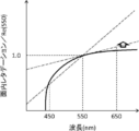
- the horizontal axis represents the wavelength of the measurement light incident on the first retardation film
- the vertical axis represents the in-plane retardation at each wavelength of the measurement light normalized by setting the in-plane retardation of the first retardation film at the measurement wavelength of 550 nm to 1.0.
- the in-plane retardation Re ( ⁇ 1) of the first retardation film at the wavelength ⁇ 1 in the wavelength range of 450 to 550 nm satisfies the following requirement 2
- the in-plane retardation Re ( ⁇ 2) of the 1 retardation film satisfies the following requirement 3.
- Requirement 2 0.0027 ⁇ ⁇ 1-0.5 ⁇ Re ( ⁇ 1) / Re (550) ⁇ 0.0009 ⁇ ⁇ 1 + 0.5 Requirement 3: 0.0009 ⁇ ⁇ 2 + 0.5 ⁇ Re ( ⁇ 2) / Re (550) ⁇ 0.0027 ⁇ ⁇ 2-0.5
- the horizontal axis represents the wavelength of the measurement light incident on the first retardation film.
- the vertical axis represents the in-plane retardation at each wavelength of the measurement light normalized by setting the in-plane retardation of the first retardation film at the measurement wavelength of 550 nm to 1.0.
- the requirement 3 is that the in-plane retardation Re ( ⁇ 2) of the first retardation film at the wavelength ⁇ 2 within the wavelength range of 550 to 650 nm is located between the straight line represented by the formula A and the straight line represented by the formula B. It means that. That is, in FIG. 1, the curve indicated by the thick line at the wavelength of 550 to 650 nm is located between the straight line represented by the formula A and the straight line represented by the formula B.
- the in-plane retardation Re ( ⁇ 1) of the first retardation film at the wavelength ⁇ 1 within the wavelength range of 450 to 550 nm satisfies the following requirement 4
- the in-plane retardation Re ( ⁇ 2) of the first retardation film at the wavelength ⁇ 2 within the wavelength range of 550 to 650 nm satisfies the following requirement 5.
- Requirement 4 0.0023 ⁇ ⁇ 1-0.25 ⁇ Re ( ⁇ 1) / Re (550) ⁇ 0.0014 ⁇ ⁇ 1 + 0.25 Requirement 5: 0.0014 ⁇ ⁇ 2 + 0.25 ⁇ Re ( ⁇ 2) / Re (550) ⁇ 0.0023 ⁇ ⁇ 2-0.25
- Two straight lines represented by solid lines in FIG. 1 are represented by the following equations.
- the requirement 5 is that the in-plane retardation Re ( ⁇ 2) of the first retardation film at the wavelength ⁇ 2 within the wavelength range of 550 to 650 nm is located between the straight line represented by the formula C and the straight line represented by the formula D. It means that. That is, in FIG. 1, the curve indicated by the thick line at the wavelength of 550 to 650 nm is located between the expressions C and D.
- the in-plane retardation Re ( ⁇ 1) of the first retardation film at the wavelength ⁇ 1 within the wavelength range of 450 to 550 nm satisfies the following requirement 10
- the in-plane retardation Re ( ⁇ 2) of the first retardation film at the wavelength ⁇ 2 within the range of 550 to 650 nm satisfies the following requirement 11.
- Requirement 10 0.0027 ⁇ ⁇ 1-0.5 ⁇ Re ( ⁇ 1) / Re (550) ⁇ 0.0014 ⁇ ⁇ 1 + 0.25 Requirement 11: 0.0009 ⁇ ⁇ 2 + 0.5 ⁇ Re ( ⁇ 2) / Re (550) ⁇ 0.0023 ⁇ ⁇ 2-0.25 Requirement 10 is that the in-plane retardation Re ( ⁇ 1) of the first retardation film at the wavelength ⁇ 1 within the wavelength range of 450 to 550 nm is located between the straight line represented by the formula A and the straight line represented by the formula D. It means that. That is, in FIG.
- the curve indicated by a thick line at a wavelength of 450 to 550 nm is located between the straight line represented by the formula A and the straight line represented by the formula D.
- the requirement 11 is that the in-plane retardation Re ( ⁇ 2) of the first retardation film at the wavelength ⁇ 2 within the wavelength range of 550 to 650 nm is located between the straight line represented by the formula B and the straight line represented by the formula C. It means that. That is, in FIG. 1, the curve indicated by the thick line at the wavelength of 550 to 650 nm is located between the expressions B and C.
- the in-plane retardation Re ( ⁇ 1) of the first retardation film at the wavelength ⁇ 1 in the wavelength range of 450 to 550 nm satisfies the following requirement 12, and the wavelength range of 550 to 650 nm, in that the effect of the present invention is more excellent. It is also preferable that the in-plane retardation Re ( ⁇ 2) of the first retardation film at the internal wavelength ⁇ 2 satisfies the following requirement 13.
- Requirement 12 0.0027 ⁇ ⁇ 1 ⁇ 0.485 ⁇ Re ( ⁇ 1) / Re (550) ⁇ 0.0009 ⁇ ⁇ 1 + 0.505 Requirement 13: 0.0009 ⁇ ⁇ 2 + 0.505 ⁇ Re ( ⁇ 2) / Re (550) ⁇ 0.0027 ⁇ ⁇ 2-0.485
- the in-plane retardation Re ( ⁇ 1) of the first retardation film at the wavelength ⁇ 1 within the wavelength range of 450 to 550 nm satisfies the following requirement 14, and the wavelength range of 550 to 650 nm.
- the in-plane retardation Re ( ⁇ 2) of the first retardation film at the internal wavelength ⁇ 2 satisfies the following requirement 15.
- Requirement 14 0.0023 ⁇ ⁇ 1 ⁇ 0.265 ⁇ Re ( ⁇ 1) / Re (550) ⁇ 0.0014 ⁇ ⁇ 1 + 0.23 Requirement 15: 0.0014 ⁇ ⁇ 2 + 0.23 ⁇ Re ( ⁇ 2) / Re (550) ⁇ 0.0023 ⁇ ⁇ 2-0.265
- the in-plane retardation Re ( ⁇ 1) of the first retardation film at the wavelength ⁇ 1 in the wavelength range of 450 to 500 nm satisfies the above requirement 2 and the first retardation film at the wavelength ⁇ 2 in the wavelength range of 600 to 650 nm is satisfied. It is also preferable that the in-plane retardation Re ( ⁇ 2) of the 1 retardation film satisfies the above requirement 3.
- the first retardation film preferably satisfies at least one of requirements 6 to 9 described later in that the effect of the present invention is more excellent.
- the thickness of the first retardation film is not particularly limited and is adjusted so that the in-plane retardation falls within a predetermined range, but from the viewpoint of thinning, it is preferably 10 ⁇ m or less, more preferably 0.5 to 8.0 ⁇ m. , 0.5 to 6.0 ⁇ m is more preferable.
- the thickness of the first retardation film means the average thickness of the first retardation film. The average thickness is obtained by measuring the thicknesses of arbitrary 5 or more points of the first retardation film and arithmetically averaging them.
- the second embodiment of the retardation film (hereinafter, also referred to as “second retardation film”) is a retardation film formed by using a liquid crystal compound and has an in-plane retardation at a wavelength of 550 nm of 100 to 200 nm. It is a retardation film that satisfies the requirements 1 and 6 described later.
- the configuration of the second retardation film will be described in detail.
- the in-plane retardation Re (550) at a wavelength of 550 nm of the second retardation film is 100 to 200 nm, and from the viewpoint that the effect of the present invention is more excellent, 120 to 160 nm is more preferable, 130 to 150 nm is further preferable, and 130 to 150 nm. 140 nm is particularly preferred.
- the retardation Rth (550) in the thickness direction of the second retardation film at a wavelength of 550 nm is not particularly limited, but is preferably 50 to 100 nm, more preferably 60 to 80 nm, further preferably 65 to 75 nm.
- the second retardation film preferably exhibits reverse wavelength dispersion.
- the reverse wavelength dispersibility is preferably shown in the visible light range. That the second retardation film exhibits reverse wavelength dispersion means that the in-plane retardation of the second retardation film increases as the measurement wavelength increases.
- Re (450), Re (550), and Re (650) described later satisfy the following relationship X. Relationship X: Re (450) ⁇ Re (550) ⁇ Re (650)
- the Re (450) / Re (550) of the second retardation film is preferably 0.75 to 0.99, and more preferably 0.80 to 0.95.
- the Re (450) / Re (550) is the in-plane retardation at the wavelength of 450 nm of the second retardation film Re (450) with respect to the Re (550) which is the in-plane retardation at the wavelength of 550 nm of the second retardation film.
- Represents the ratio of The Re (650) / Re (550) of the second retardation film is preferably 1.03 to 1.20, more preferably 1.08 to 1.15.
- the Re (650) / Re (550) is an in-plane retardation at a wavelength of 650 nm of the first retardation film Re (650) with respect to an in-plane retardation at a wavelength of 550 nm of the second retardation film Re (550). Represents the ratio of
- ⁇ xy ((x ⁇ x0) 2 + (y ⁇ y0) 2 ) 1/2
- x and y represent chromaticity coordinates on the CIExy chromaticity diagram of the transmitted light of the second retardation film
- x0 and y0 represent chromaticity coordinates of the standard light source D65 (light of the standard light source D65) on the CIExy chromaticity diagram.
- the above-mentioned ⁇ xy is preferably 0.008 or less in that the reflection tint is further reduced.
- the lower limit of ⁇ xy is not particularly limited, but is often 0.001 or more.
- the method for measuring the chromaticity is as follows.
- the transmittance of the film was measured at intervals of 10 nm in the wavelength range of 380 to 780 nm, and the obtained value was multiplied by the spectral distribution of the standard light source D65 to obtain the value at each wavelength. Calculate the transmitted light intensity distribution.
- the obtained transmitted light intensity is multiplied by the CIE spectrum tristimulus value (see, for example, "Science of Color, Psychology, Physiology, and Physics" written by Takayoshi Kaneko), and the values are summed at all wavelengths to obtain X, Y, Z, respectively.
- the horizontal axis represents the wavelength of the measurement light incident on the second retardation film
- the vertical axis represents the in-plane retardation of the second retardation film at the wavelengths of the measurement light of 25 nm in the wavelength range of 450 to 600 nm
- the slope S of a straight line connecting two adjacent plot points satisfies the requirement 6.
- Requirement 6 0.10 ⁇ Slope S ⁇ 1.0
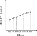
- the requirement 6 will be described in detail with reference to the drawings.
- the horizontal axis represents the wavelength of the measurement light incident on the second retardation film.
- the vertical axis represents the in-plane retardation (nm) of the second retardation film at the wavelength of the measurement light.
- the in-plane retardation of the second retardation film at each wavelength of the measurement light is plotted.
- the measurement is performed with measuring light at every 25 nm in the wavelength range of 450 to 600 nm. That is, as shown in FIG. 2, the in-plane retardations of the measurement lights of wavelength 450 nm, wavelength 475 nm, wavelength 500 nm, wavelength 525 nm, wavelength 550 nm, wavelength 575 nm, and wavelength 600 nm are obtained and plotted on the graph.
- two adjacent plot points are connected by a straight line. More specifically, as shown in FIG.
- a plot point at a wavelength of 450 nm and a plot point at a wavelength of 475 nm are connected by a straight line (straight line 1), and a plot point at a wavelength of 475 nm and a plot point at a wavelength of 500 nm are connected.
- a straight line straight line 2
- a plot point at a wavelength of 500 nm and a plot point at a wavelength of 525 nm are connected by a straight line (straight line 3)
- a plot point at a wavelength of 525 nm and a plot point at a wavelength of 550 nm are drawn by a straight line (straight line).
- the plot point at the wavelength of 550 nm and the plot point at the wavelength of 575 nm are joined by a straight line (straight line 5), and the plot point at the wavelength of 575 nm and the plot point at a wavelength of 600 nm are joined by a straight line (straight line 6). ..
- the slope S of each obtained straight line is calculated. If all the obtained slopes S (the slopes S of the straight lines 1 to 6) are more than 0.10 and 1.0 or less, the requirement 6 is satisfied.
- the second retardation film at the wavelength of the measurement light at every 25 nm in the wavelength range of 450 to 650 nm.
- the slope S of the straight line connecting two adjacent plot points both satisfy the requirement 7.
- Requirement 7 0.10 ⁇ Slope S ⁇ 1.0
- in-plane retardation in the measurement light of wavelength 450 nm, wavelength 475 nm, wavelength 500 nm, wavelength 525 nm, wavelength 550 nm, wavelength 575 nm, wavelength 600 nm, wavelength 625 nm, and wavelength 650 nm. , And plot them on the graph.
- the inclination of each of the straight lines 1 to 6 the plot point at the wavelength of 600 nm and the plot point at the wavelength of 625 nm, the slope of the straight line (straight line 7), and the plot point at the wavelength of 625 nm and the plot point at the wavelength of 650 nm It is preferable that the inclination of the straight line (straight line 8) satisfies the requirement 7.
- the slope S (550) of the straight line connecting the plot point where the measurement light has the wavelength of 550 nm and the plot point where the measurement light has the wavelength of 575 nm (the slope S of the straight line 5) Preferably satisfies the requirement 8.
- the slope S (625) of the straight line connecting the plot point where the measurement light has the wavelength of 625 nm and the plot point where the measurement light has the wavelength of 650 nm (the slope S of the straight line 8) Preferably satisfies the requirement 9.
- the retardation film (first retardation film and second retardation film) is a layer formed using at least a liquid crystal compound.
- the retardation film is preferably a film obtained by fixing the liquid crystal compound by homogeneously aligning it.
- a rigid flat type is the mainstream of organic electroluminescence display panels (organic EL display panels).
- organic EL display panels organic electroluminescence display panels
- a foldable flexible organic EL display panel has been proposed.
- the circularly polarizing plate used for such a flexible organic EL display panel is required to have excellent flexibility in itself. From this point of view, a retardation film formed using a liquid crystal compound is more flexible than a polymer film, and thus can be suitably applied to a flexible organic EL display panel.
- the type of liquid crystal compound is not particularly limited, but depending on its shape, it can be classified into a rod-shaped type (rod-shaped liquid crystal compound) and a disc-shaped type (disc-shaped liquid crystal compound. Discotic liquid crystal compound). Further, there are low molecular type and high molecular type respectively.
- a polymer has a degree of polymerization of 100 or more (polymer physics / phase transition dynamics, Masao Doi, p. 2, Iwanami Shoten, 1992). Two or more rod-shaped liquid crystal compounds, two or more discotic liquid crystal compounds, or a mixture of a rod-shaped liquid crystal compound and a discotic liquid crystal compound may be used.
- the liquid crystal compound is more preferably formed by using a liquid crystal compound having a polymerizable group (a rod-shaped liquid crystal compound or a discotic liquid crystal compound) because it can reduce the temperature change and the humidity change of the optical properties.
- the liquid crystal compound may be a mixture of two or more kinds, and in that case, it is preferable that at least one has two or more polymerizable groups. That is, the liquid crystal compound is preferably a layer formed by fixing a liquid crystal compound having a polymerizable group (a rod-shaped liquid crystal compound or a discotic liquid crystal compound) by polymerization or the like. It does not need to exhibit liquid crystallinity.
- the type of the polymerizable group is not particularly limited, and a polymerizable group capable of radical polymerization or cationic polymerization is preferable.
- a polymerizable group capable of radical polymerization or cationic polymerization is preferable.
- a known radically polymerizable group can be used, and an acryloyl group or a methacryloyl group is preferable.
- a known cationically polymerizable group a known cationically polymerizable group can be used, and specifically, an alicyclic ether group, a cyclic acetal group, a cyclic lactone group, a cyclic thioether group, a spiro orthoester group, and vinyloxy. Groups and the like. Of these, an alicyclic ether group or a vinyloxy group is preferable, and an epoxy group, an oxetanyl group, or a vinyloxy group is more preferable.
- preferable polymerizable groups include the
- the liquid crystal compound preferably exhibits reverse wavelength dispersion.
- the liquid crystal compound having reverse wavelength dispersion means that the liquid crystal compound has a main chain mesogen and a side chain mesogen bonded to the main chain mesogen in the molecule, and the main chain mesogen and the side chain when aligned uniformly. It means a compound in which the optical axis with respect to mesogen is oriented in a different direction so that the birefringence ⁇ n exhibits reverse wavelength dispersion characteristics. That is, the "reverse wavelength dispersion" liquid crystal compound is a liquid crystal compound that is measured when an in-plane retardation (Re) value at a specific wavelength (visible light range) of an optically anisotropic layer produced using this compound is measured.
- Re in-plane retardation
- the main chain mesogen means a mesogen located in the major axis direction in the molecule, and the side chain mesogen binds to the main chain mesogen and has a different optical axis (for example, orthogonal to the major axis direction).
- Direction means a mesogen.
- the structure surrounded by a corresponds to the main chain mesogen
- the structure surrounded by b corresponds to the side chain mesogen.
- D 1 , D 2 , D 3 and D 4 are each independently a single bond, —O—, —CO—, —O—CO—, —C ( ⁇ S) O—, -CR 1 R 2 -, - CR 1 R 2 -CR 3 R 4 -, - O-CR 1 R 2 -, - CR 1 R 2 -O-CR 3 R 4 -, - CO-O-CR 1 R 2 -, - O-CO- CR 1 R 2 -, - CR 1 R 2 -CR 3 R 4 -O-CO -, - CR 1 R 2 -O-CO-CR 3
- R 1 , R 2 , R 3 and R 4 each independently represent a hydrogen atom, a fluorine atom or an alkyl group having 1 to 4 carbon atoms.
- the plurality of R 1 , the plurality of R 2 , the plurality of R 3 and the plurality of R 4 may be the same or different from each other.
- G 1 and G 2 are each independently linked to a divalent alicyclic hydrocarbon group having 5 to 8 carbon atoms and a plurality of the above alicyclic hydrocarbon groups.
- the group formed by connecting a plurality of the alicyclic hydrocarbon groups means a group formed by connecting divalent alicyclic hydrocarbon groups having 5 to 8 carbon atoms with a single bond. Further, the group formed by connecting a plurality of the aromatic hydrocarbon groups means a group formed by connecting aromatic hydrocarbon groups with a single bond.
- a 1 and A 2 each independently represent a single bond, an aromatic ring having 6 or more carbon atoms, or a cycloalkylene ring having 6 or more carbon atoms.
- SP 1 and SP 2 are each independently a single bond, a linear or branched alkylene group having 1 to 14 carbon atoms, or a linear chain having 1 to 14 carbon atoms. At least one of —CH 2 — constituting a branched or branched alkylene group is replaced by —O—, —S—, —NH—, —N (Q) —, or —CO— Represents a linking group, and Q represents a polymerizable group.
- L 1 and L 2 each independently represent a monovalent organic group (for example, an alkyl group or a polymerizable group).
- Ar is a group represented by the formula (Ar-1), a group represented by the formula (Ar-2), a group represented by the formula (Ar-4), or a group represented by the formula (Ar-5) described later.
- a group represented by the formula (Ar-6) or a group represented by the formula (Ar-7) at least one of L 1 and L 2 represents a polymerizable group.
- Ar is a group represented by the formula (Ar-3) described later, at least one of L 1 and L 2 and L 3 and L 4 in the formula (Ar-3) below is a polymerizable group.
- the divalent alicyclic hydrocarbon group having 5 to 8 carbon atoms represented by G 1 and G 2 is preferably a 5-membered ring or a 6-membered ring.
- the alicyclic hydrocarbon group may be a saturated alicyclic hydrocarbon group or an unsaturated alicyclic hydrocarbon group, but a saturated alicyclic hydrocarbon group is preferable.
- the divalent alicyclic hydrocarbon group represented by G 1 and G 2 for example, the description in paragraph 0078 of JP 2012-21068 A can be referred to, and the contents thereof are incorporated in the present specification.
- Examples of the aromatic ring having 6 or more carbon atoms represented by A 1 and A 2 in the above formula (I) include aromatic hydrocarbon rings such as benzene ring, naphthalene ring, anthracene ring, and phenanthroline ring; Ring, pyrrole ring, thiophene ring, pyridine ring, thiazole ring, and aromatic heterocycle such as benzothiazole ring; Of these, a benzene ring (eg, 1,4-phenyl group) is preferable.
- examples of the cycloalkylene ring having 6 or more carbon atoms represented by A 1 and A 2 include a cyclohexane ring and a cyclohexene ring, and among them, a cyclohexane ring (for example, cyclohexane ring). -1,4-diyl group and the like) are preferable.
- the linear or branched alkylene group having 1 to 14 carbon atoms represented by SP 1 and SP 2 is preferably a methylene group, an ethylene group, a propylene group, or a butylene group.
- the polymerizable groups represented by L 1 and L 2 are not particularly limited, but may be a radical polymerizable group (radical polymerizable group) or a cation polymerizable group (cation polymerizable group). preferable.
- the suitable range of the radically polymerizable group is as described above.
- Ar represents any aromatic ring selected from the group consisting of groups represented by the following formulas (Ar-1) to (Ar-7).
- formulas (Ar-1) to (Ar-7) below * 1 represents a bonding position with D 1 and * 2 represents a bonding position with D 2 .
- Q 1 represents N or CH
- Q 2 represents —S—, —O—, or —N (R 5 ) —
- R 5 is Represents a hydrogen atom or an alkyl group having 1 to 6 carbon atoms
- Y 1 represents an aromatic hydrocarbon group having 6 to 12 carbon atoms or an aromatic hetero group having 3 to 12 carbon atoms, which may have a substituent. Represents a ring group.
- Examples of the alkyl group having 1 to 6 carbon atoms represented by R 5 include methyl group, ethyl group, propyl group, isopropyl group, n-butyl group, isobutyl group, sec-butyl group, tert-butyl group, n-pentyl group. Group and n-hexyl group.
- Examples of the aromatic hydrocarbon group having 6 to 12 carbon atoms represented by Y 1 include a phenyl group, a 2,6-diethylphenyl group, and an aryl group such as a naphthyl group.
- Examples of the aromatic heterocyclic group having 3 to 12 carbon atoms represented by Y 1 include a thienyl group, a thiazolyl group, a furyl group, a pyridyl group, and a heteroaryl group such as a benzofuryl group.
- the aromatic heterocyclic group also includes a group in which a benzene ring and an aromatic heterocycle are condensed.
- examples of the substituent that Y 1 may have include an alkyl group, an alkoxy group, a nitro group, an alkylsulfonyl group, an alkyloxycarbonyl group, a cyano group, and a halogen atom.
- alkyl group for example, a linear, branched or cyclic alkyl group having 1 to 18 carbon atoms is preferable, and an alkyl group having 1 to 8 carbon atoms (eg, methyl group, ethyl group, propyl group, isopropyl group , N-butyl group, isobutyl group, sec-butyl group, t-butyl group, and cyclohexyl group) are more preferable, an alkyl group having 1 to 4 carbon atoms is further preferable, and a methyl group or an ethyl group is particularly preferable.
- an alkyl group having 1 to 8 carbon atoms eg, methyl group, ethyl group, propyl group, isopropyl group , N-butyl group, isobutyl group, sec-butyl group, t-butyl group, and cyclohexyl group
- an alkyl group having 1 to 4 carbon atoms is
- an alkoxy group having 1 to 18 carbon atoms is preferable, and an alkoxy group having 1 to 8 carbon atoms (eg, methoxy group, ethoxy group, n-butoxy group, and methoxyethoxy group) is more preferable, An alkoxy group having 1 to 4 carbon atoms is more preferable, and a methoxy group or an ethoxy group is particularly preferable.
- the halogen atom include a fluorine atom, a chlorine atom, a bromine atom, and an iodine atom, and a fluorine atom or a chlorine atom is preferable.
- Z 1 , Z 2 and Z 3 are each independently a hydrogen atom, a monovalent aliphatic hydrocarbon group having 1 to 20 carbon atoms, or a carbon atom.
- a monovalent alicyclic hydrocarbon group having 3 to 20 carbon atoms, a monovalent aromatic hydrocarbon group having 6 to 20 carbon atoms, a halogen atom, a cyano group, a nitro group, -NR 6 R 7 or -SR 8 R 6 to R 8 each independently represent a hydrogen atom or an alkyl group having 1 to 6 carbon atoms, and Z 1 and Z 2 may be bonded to each other to form a ring.
- the ring may be any of an alicyclic ring, a heterocyclic ring, and an aromatic ring, and is preferably an aromatic ring.
- the formed ring may be substituted with a substituent.
- the monovalent aliphatic hydrocarbon group having 1 to 20 carbon atoms an alkyl group having 1 to 15 carbon atoms is preferable, an alkyl group having 1 to 8 carbon atoms is more preferable, and a methyl group, an ethyl group, an isopropyl group, tert.
- -Pentyl group (1,1-dimethylpropyl group), tert-butyl group, or 1,1-dimethyl-3,3-dimethyl-butyl group is more preferable, and methyl group, ethyl group, or tert-butyl group Is particularly preferable.
- Examples of the monovalent alicyclic hydrocarbon group having 3 to 20 carbon atoms include cyclopropyl group, cyclobutyl group, cyclopentyl group, cyclohexyl group, cycloheptyl group, cyclooctyl group, cyclodecyl group, methylcyclohexyl group, and Monocyclic saturated hydrocarbon group such as ethylcyclohexyl group; cyclobutenyl group, cyclopentenyl group, cyclohexenyl group, cycloheptenyl group, cyclooctenyl group, cyclodecenyl group, cyclopentadienyl group, cyclohexadienyl group, cyclooctadienyl group, And monocyclic unsaturated hydrocarbon groups such as cyclodecadiene group; bicyclo [2.2.1] heptyl group, bicyclo [2.2.2] oct
- the monovalent aromatic hydrocarbon group having 6 to 20 carbon atoms include a phenyl group, a 2,6-diethylphenyl group, a naphthyl group, a biphenyl group and the like, and an aryl group having 6 to 12 carbon atoms. (In particular, a phenyl group) is preferable.
- the halogen atom include a fluorine atom, a chlorine atom, a bromine atom, an iodine atom and the like, and a fluorine atom, a chlorine atom or a bromine atom is preferable.
- examples of the alkyl group having 1 to 6 carbon atoms represented by R 6 to R 8 include, for example, methyl group, ethyl group, propyl group, isopropyl group, n-butyl group, isobutyl group, sec-butyl group, tert-butyl group. Group, n-pentyl group, and n-hexyl group.
- a 3 and A 4 are independently from —O—, —N (R 9 ) —, —S—, and —CO—. consisting represents a group selected from the group, R 9 represents a hydrogen atom or a substituent. Examples of the substituent represented by R 9 include those similar to the substituent that Y 1 in the above formula (Ar-1) may have.
- X represents a hydrogen atom or a non-metal atom of Group 14 to 16 to which a substituent may be bonded.
- the non-metal atoms of Groups 14 to 16 represented by X include an oxygen atom, a sulfur atom, a nitrogen atom having a substituent, and a carbon atom having a substituent. Examples thereof include the same substituents as Y 1 in formula (Ar-1) may have.
- -C ( S) O - , - CR 1 R 2 -, - CR 1 R 2 -CR 3 R 4 -, - O-CR 1 R 2 -, - CR 1 R 2 -O-CR 3 R 4 -, - CO-O-CR 1 R 2 -, - O-CO-CR 1 R 2 -, - CR 1 R 2 -O-CO-CR 3 R 4 -, - CR 1 R 2 -CO-O- It represents CR 3 R 4 —, —NR 1 —CR 2 R 3 —, or —CO—NR 1 —.
- R 1 , R 2 , R 3 and R 4 each independently represent a hydrogen atom, a fluorine atom or an alkyl group having 1 to 4 carbon
- SP 3 and SP 4 are each independently a single bond, a linear or branched alkylene group having 1 to 12 carbon atoms, or a C 1 to 12 carbon atom.
- One or more of —CH 2 — constituting the linear or branched alkylene group is substituted with —O—, —S—, —NH—, —N (Q) —, or —CO— It represents a divalent linking group, and Q represents a polymerizable group.
- L 3 and L 4 each independently represent a monovalent organic group (eg, an alkyl group or a polymerizable group), and as described above, L 3 and L 4 are 4 and at least one of L 1 and L 2 in the above formula (I) represents a polymerizable group.
- the monovalent organic group other than the polymerizable group include an alkyl group, an aryl group, and a heteroaryl group.
- Ax has at least one aromatic ring selected from the group consisting of aromatic hydrocarbon rings and aromatic heterocycles, and has 2 to 30 carbon atoms.
- Ay is a hydrogen atom, an alkyl group having 1 to 6 carbon atoms which may have a substituent, or an aromatic hydrocarbon ring and an aromatic group. It represents an organic group having 2 to 30 carbon atoms and having at least one aromatic ring selected from the group consisting of group heterocycles.
- the aromatic ring in Ax and Ay may have a substituent, and Ax and Ay may combine with each other to form a ring.
- Q 3 represents a hydrogen atom or an optionally substituted alkyl group having 1 to 6 carbon atoms.
- Ax and Ay include those described in paragraphs 0039 to 0095 of WO 2014/010325.
- Examples of the alkyl group having 1 to 6 carbon atoms represented by Q 3 include, for example, methyl group, ethyl group, propyl group, isopropyl group, n-butyl group, isobutyl group, sec-butyl group, tert-butyl group, n Examples thereof include a pentyl group and an n-hexyl group, and examples of the substituent include those similar to the substituent that Y 1 in the above formula (Ar-1) may have.
- At least one of A 1 and A 2 is preferably a cycloalkylene ring having 6 or more carbon atoms, and one of A 1 and A 2 is 6 or more carbon atoms, because the effect of the present invention is more excellent.
- the retardation film may be formed by combining other components than the liquid crystal compound. That is, the retardation film may contain a component other than the component derived from the liquid crystal compound.
- the retardation film may contain a dye. That is, the retardation film may be a layer formed using a composition containing a liquid crystal compound and a dye. The inclusion of the dye makes it possible to control the wavelength dispersion of the retardation film.
- the retardation film contains an infrared absorbing dye will be described in detail.
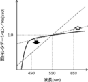
- 3 shows the wavelength dispersion characteristics of the in-plane retardation at each wavelength in the visible light region standardized by setting the in-plane retardation at the measurement wavelength of 550 nm to 1.0, and meets the requirements 2 and 3 described above with broken lines. Shows a straight line.
- a conventional retardation film exhibiting reverse wavelength dispersion satisfies requirements 2 and 3 in a short wavelength region of 550 nm or less, but satisfies requirement 2 in a long wavelength region of 550 nm or more, as shown by a solid line in FIG. In many cases, there is a tendency that 3 and 3 are not satisfied.
- an infrared absorbing dye is used, and by controlling the absorption characteristics of the retardation film at a wavelength of 700 to 900 nm, optical characteristics in the long wavelength region are required, as indicated by white arrows. It can be adjusted to satisfy 2 and 3.
- the refractive index wavelength dispersion characteristics of a general organic molecule In FIG. 4, the upper side shows the behavior of the refractive index with respect to the wavelength, and the lower side shows the behavior of the absorption characteristic with respect to the wavelength (absorption spectrum).
- the refractive index n in the region away from the intrinsic absorption wavelength region a in FIG. 4 monotonically decreases as the wavelength increases.
- Such dispersion is called "normal dispersion”.
- the refractive index n in the wavelength region including the intrinsic absorption (region of b in FIG. 4) sharply increases as the wavelength increases.
- Such dispersion is called "abnormal dispersion”. That is, as shown in FIG. 4, an increase or decrease in the refractive index is observed immediately before the absorption wavelength range.
- the retardation film is affected by the infrared absorbing dye, and absorption at a wavelength of 700 to 900 nm in the direction of the fast axis of the retardation film. Is larger than the absorption at the wavelength of 700 to 900 nm in the direction of the slow axis of the retardation film.
- an absorption characteristic is also referred to as an absorption characteristic X.
- the absorption characteristic X is achieved by arranging in the retardation film the axial direction in which the infrared absorbing dye has a high absorbance in parallel with the fast axis direction of the retardation film.
- the retardation film showing the absorption characteristic X has a lower ordinary ray refractive index than the retardation film having no absorption characteristic X.
- FIG. 5 is a diagram showing a comparison of wavelength dispersion between the extraordinary ray refractive index ne and the ordinary ray refractive index no depending on the presence or absence of the absorption characteristic X.
- the thick line shows the curve of the extraordinary ray refractive index ne without the absorption characteristic X
- the solid line shows the curve of the ordinary ray refractive index no without the absorption characteristic X.
- the retardation film having the absorption characteristic X is affected by the absorption at the wavelength of 700 to 900 nm as shown in FIG.
- the dichroic dye which has a maximum absorption wavelength in a visible light region (henceforth "a visible light absorption dichroic dye” is also called. ) Is used.
- a visible light absorption dichroic dye When the visible light absorbing dichroic dye is present in the retardation film, it affects the wavelength dispersibility of the retardation film as in the case of using the above infrared absorbing dye.
- a retardation film is prepared by using a dichroic dye having a maximum absorption wavelength near 550 nm together with a liquid crystal compound, it is affected by the refractive index wavelength dispersion characteristics shown in FIG.
- a black arrow indicates in the short wavelength region of 550 nm or less.
- the curve moves in the direction of the white arrow in the long wavelength region of 550 nm or more, and the retardation film satisfying the above requirements 2 and 3 (or requirement 6) is obtained.
- the infrared absorbing dye is not particularly limited as long as it is a dye that absorbs infrared rays (in particular, light having a wavelength of 700 to 900 m).
- the infrared absorbing dye is preferably a dichroic dye.
- the dichroic dye means a dye having a property that the absorbance in the major axis direction of the molecule and the absorbance in the minor axis direction are different.
- Infrared absorbing dyes include diketopyrrolopyrrole dyes, diimmonium dyes, phthalocyanine dyes, naphthalocyanine dyes, azo dyes, polymethine dyes, anthraquinone dyes, pyrylium dyes, squarylium dyes, triphenylmethane dyes. Examples thereof include dyes, cyanine dyes, and aminium dyes.
- the infrared absorbing dyes may be used alone or in combination of two or more.
- the infrared absorbing dye preferably has a mesogenic group.
- the infrared absorbing dye has a mesogenic group, it is easily aligned with the above-mentioned liquid crystal compound, and it is easy to control a predetermined absorption characteristic.
- the mesogen group is a functional group having rigidity and orientation.
- the mesogen group for example, a group selected from the group consisting of an aromatic ring group (aromatic hydrocarbon ring group and aromatic heterocyclic group) and an alicyclic group, a plurality of groups, direct or linking group (for example, Examples thereof include a structure linked via —CO—, —O—, —NR— (R represents a hydrogen atom or an alkyl group), or a group combining these.
- the maximum absorption wavelength of the infrared absorbing dye is preferably located in the range of 700 to 900 nm from the viewpoint that the effect of the present invention is more excellent.
- a preferred form of the infrared absorbing dye is a compound represented by the formula (1).
- the compound represented by the formula (1) has a small absorption in the visible light region, and further suppresses coloring of the obtained retardation film. Further, since this compound contains a group having a mesogenic group, it is easily aligned with the liquid crystal compound. At that time, since the group having a mesogenic group is arranged in a form extending laterally from the condensed ring portion containing a nitrogen atom in the center of the compound, the above-mentioned condensed It is easy to arrange the ring parts in a direction orthogonal to each other.
- absorption in the infrared region (particularly, wavelength of 700 to 900 nm) derived from the condensed ring portion is easily obtained in the direction orthogonal to the slow axis of the retardation film, and a retardation film having desired characteristics is easily obtained. ..
- R 11 and R 12 each independently represent a hydrogen atom or a substituent, at least one of which is an electron-withdrawing group, and R 11 and R 12 may combine with each other to form a ring.
- substituents include an alkyl group, an alkenyl group, an alkynyl group, an aryl group, an amino group, an alkoxy group, an aryloxy group, an aromatic heterocyclic oxy group, an acyl group, an alkoxycarbonyl group, an aryloxycarbonyl group, an acyloxy group.
- R 11 and R 12 are preferably a group other than the group having a mesogen group described later.
- the electron-withdrawing group represents a substituent having a positive Hammett's ⁇ p value (sigmapara value), and examples thereof include a cyano group, an acyl group, an alkyloxycarbonyl group, an aryloxycarbonyl group, a sulfamoyl group, a sulfinyl group, and a hetero group. A ring group is mentioned. These electron-withdrawing groups may be further substituted.
- the Hammett's substituent constant ⁇ value will be described. Hammett's rule is used to quantitatively discuss the effect of substituents on the reaction or equilibrium of benzene derivatives in 1935 L.A. P. The rule of thumb proposed by Hammett, which is widely accepted today.
- Substituent constants determined by Hammett's law include ⁇ p values and ⁇ m values, and these values can be found in many general texts. For example, J. A. Dean ed., “Lange's Handbook of Chemistry”, 12th Edition, 1979 (McGraw-Hill) and “Chemistry” extra number, 122, 96-103, 1979 (Nankodo), Chem. Rev. , 1991, Volume 91, pp. 165-195.
- the electron-withdrawing group is preferably a substituent having a Hammett's substituent constant ⁇ p value of 0.20 or more.
- the ⁇ p value is preferably 0.25 or more, more preferably 0.30 or more, still more preferably 0.35 or more.
- the upper limit is not particularly limited, but 0.80 or less is preferable.
- Specific examples include a cyano group (0.66), a carboxyl group (-COOH: 0.45), an alkoxycarbonyl group (-COOMe: 0.45), an aryloxycarbonyl group (-COOPh: 0.44), carbamoyl.
- Me represents a methyl group
- Ph represents a phenyl group.
- the values in parentheses are ⁇ p values of typical substituents in Chem. Rev. , 1991, vol. 91, pp. 165-195.
- R 11 and R 12 When R 11 and R 12 are combined to form a ring, they form a 5 to 7 membered ring (preferably 5 to 6 membered ring), and the formed ring is usually a merocyanine dye and used as an acidic nucleus. Those that can be used are preferred.
- the ring formed by combining R 11 and R 12 includes 1,3-dicarbonyl nucleus, pyrazolinone nucleus, 2,4,6-triketohexahydropyrimidine nucleus (including thioketone body), 2-thio- 2,4-thiazolidinedione nucleus, 2-thio-2,4-oxazolidinedione nucleus, 2-thio-2,5-thiazolidinedione nucleus, 2,4-thiazolidinedione nucleus, 2,4-imidazolidinedione nucleus, 2 A -thio-2,4-imidazolidinedione nucleus, a 2-imidazolin-5-one nucleus, a 3,5-pyrazolidinedione nucleus, a benzothiophen-3-one nucleus, or an indanone nucleus is preferable.
- R 11 is preferably a heterocyclic group, and more preferably an aromatic heterocyclic group.
- the heterocyclic group may be monocyclic or polycyclic.
- a substituent may be substituted on the heterocyclic group. Examples of the substituent include the examples of the substituents exemplified as the above-mentioned substituent
- R 13 independently represents a hydrogen atom, an alkyl group, an aryl group, a heteroaryl group, a substituted boron (—B (Ra) 2 , Ra represents a substituent) or a metal atom, and a covalent bond with R 11 or It may be coordinate-bonded.
- the substituent of the substituted boron represented by R 13 has the same meaning as the substituent described above for R 11 and R 12 , and is preferably an alkyl group, an aryl group or a heteroaryl group.
- the substituent of the substituted boron (for example, the above-described alkyl group, aryl group, or heteroaryl group) may be further substituted with a substituent.
- the substituent examples include the groups exemplified as the substituents represented by R 11 and R 12 .
- the metal atom represented by R 13 is preferably a transition metal atom, a magnesium atom, an aluminum atom, a calcium atom, a barium atom, a zinc atom, or a tin atom, and an aluminum atom, a zinc atom, a tin atom, a vanadium atom, An iron atom, a cobalt atom, a nickel atom, a copper atom, a palladium atom, an iridium atom, or a platinum atom is more preferable.
- R 14's each independently represent a group having a mesogenic group.
- the definition of the mesogenic group is as described above.
- R 14 is preferably a group represented by formula (2). * Represents a binding position.
- Formula (2) * -M 1- (X 1 -M 2 ) n -X 2 -P M 1 represents a substituted or unsubstituted arylene group or a substituted or unsubstituted heteroarylene group.
- a phenylene group is mentioned as an arylene group.
- heteroarylene group examples include a pyrazole ring, a thiazole ring, an oxazole ring, an imidazole ring, an oxadiazole ring, a thiadiazole ring, a triazole ring, a pyridine ring, a pyridazine ring, a pyrimidine ring, a pyrazine ring, and a benzo condensed ring thereof (for example, benzo Examples thereof include a thiazole ring, a benzopyrazine ring) or a naphtho-condensed ring, or a divalent group obtained by removing any two hydrogen atoms from a complex of these condensed rings.
- R 0 represents a hydrogen atom or an alkyl group having 1 to 5 carbon atoms.
- M 2 represents a substituted or unsubstituted arylene group, a substituted or unsubstituted heteroarylene group, or a substituted or unsubstituted cycloalkylene group.
- a phenylene group is mentioned as an arylene group.
- heteroarylene group examples include a pyrazole ring, a thiazole ring, an oxazole ring, an imidazole ring, an oxadiazole ring, a thiadiazole ring, a triazole ring, a pyridine ring, a pyridazine ring, a pyrimidine ring, a pyrazine ring, and a benzo condensed ring thereof (for example, benzo Examples thereof include a thiazole ring, a benzopyrazine ring) or a naphtho-condensed ring, or a divalent group obtained by removing any two hydrogen atoms from a complex of these condensed rings.
- the cycloalkylene group preferably has 5 to 7 carbon atoms.
- substituents represented by R 11 and R 12 examples of the substituent include the groups exemplified by the substituents represented by R 11 and R 12 .
- X 2 represents a single bond or a divalent linking group.
- the divalent linking group include a divalent hydrocarbon group (eg, an alkylene group having 1 to 10 carbon atoms, an alkenylene group having 1 to 10 carbon atoms, and an alkynylene group having 1 to 10 carbon atoms).
- Divalent aromatic hydrocarbon group divalent aromatic hydrocarbon group such as arylene group
- divalent heterocyclic group divalent heterocyclic group
- Q represents a hydrogen atom or an alkyl group.
- n represents 1 to 10. Among them, 1 to 5 is preferable, and 2 to 4 is more preferable.
- P represents a hydrogen atom or a polymerizable group.
- the definition of the polymerizable group is synonymous with the definition of the polymerizable group that the liquid crystal compound described later may have.
- the infrared absorbing dye is more preferably a compound represented by the formula (3).
- R 14 is as described above.
- R 22's each independently represent a cyano group, an acyl group, an alkoxycarbonyl group, an alkylsulfinyl group, an arylsulfinyl group, or a nitrogen-containing heteroaryl group.
- R 15 and R 16 each independently represent a hydrogen atom, an alkyl group, an alkoxy group, an aryl group, or a heteroaryl group, and R 15 and R 16 may combine with each other to form a ring. Examples of the ring formed include an alicyclic ring having 5 to 10 carbon atoms, an aromatic hydrocarbon ring having 6 to 10 carbon atoms, and an aromatic heterocyclic ring having 3 to 10 carbon atoms.
- the ring formed by combining R 15 and R 16 may be further substituted with a substituent.
- substituents include the groups exemplified in the description of the substituent represented by R 11 and R 12 .
- R 17 and R 18 each independently represent an alkyl group, an alkoxy group, an aryl group, or a heteroaryl group.
- the group represented by R 17 and R 18 may be further substituted with a substituent.
- substituent include the groups exemplified in the description of the substituent represented by R 11 and R 12 .
- X independently represents an oxygen atom, a sulfur atom, —NR—, —CRR′—, —CH ⁇ CH—, or —N ⁇ CH—, and R and R ′ are each independently a hydrogen atom. Represents an alkyl group or an aryl group.
- the visible light absorbing dichroic dye is not particularly limited, and examples thereof include acridine dye, azine dye, azomethine dye, oxazine dye, cyanine dye, merocyanine dye, squarylium dye, naphthalene dye, azo dye, and anthraquinone dye, benzotriazole dye.
- Benzophenone dye pyrazoline dye, diphenylpolyene dye, binaphthylpolyene dye, stilbene dye, benzothiazole dye, thienothiazole dye, benzimidazole dye, coumarin dye, nitrodiphenylamine dye, polymethine dye, naphthoquinone dye, perylene dye, quinophthalone dye, stilbene Pigments and indigo pigments.
- the dichroic ratio of a visible light absorbing dichroic dye is defined by the ratio of the absorbance at the maximum absorption wavelength in the long axis direction of the visible light absorbing dichroic dye to the absorbance in the short axis direction.
- the dichroic ratio can be determined by measuring the absorbance in the alignment direction of the visible light absorbing dichroic dye and the absorbance in the direction perpendicular to the alignment direction.
- the dichroic ratio of the visible light absorbing dichroic dye is preferably from 2 to 50, more preferably from 5 to 30.
- the visible light absorbing dichroic dye may have a polymerizable group.
- the polymerizable group include an acrylic group, a methacrylic group, a vinyl group, a vinyloxy group, an epoxy group, and an oxetanyl group.
- the maximum absorption wavelength of the visible light absorbing dichroic dye is preferably in the range of 400 to 700 nm, more preferably in the range of 540 to 620 nm.
- the method for producing the retardation film is not particularly limited, and known methods can be used. Among them, a liquid crystal compound having a polymerizable group (hereinafter also simply referred to as “polymerizable liquid crystal compound”) and the above-mentioned dye (for example, an infrared absorbing dye or visible light) from the viewpoint of easily controlling the wavelength dispersion characteristics of the retardation film.
- a composition for forming a retardation film containing an absorbing dichroic dye hereinafter also simply referred to as "composition" is applied to form a coating film, and the coating film is subjected to an alignment treatment to align the polymerizable liquid crystal compound.
- a method of forming a retardation film by subjecting the obtained coating film to a curing treatment is preferable.
- a curing treatment ultraviolet irradiation (light irradiation treatment) or heat treatment
- the composition is applied onto a support to form a coating film, and the coating film is subjected to an alignment treatment to align the polymerizable liquid crystal compound.
- the dye is also oriented in a predetermined direction according to the orientation of the polymerizable liquid crystal compound.
- the composition used comprises a polymerizable liquid crystal compound.
- the definition of the polymerizable liquid crystal compound is as described above.
- the composition used also contains a dye such as an infrared absorbing dye or a visible light absorbing dichroic dye.
- the content of the polymerizable liquid crystal compound in the composition is not particularly limited, but is preferably 50% by mass or more, more preferably 70% by mass or more, and further preferably 90% by mass or more, based on the total solid content in the composition. ..
- the upper limit is not particularly limited, but is often 99% by mass or less.
- the solvent is not included in the total solid content in the composition.
- the content of the dye in the composition is not particularly limited, but when the composition contains an infrared absorbing dye, the content of the infrared absorbing dye is 1 to 20 parts by mass with respect to 100 parts by mass of the polymerizable liquid crystal compound. Is preferable, and 3 to 15 parts by mass is more preferable.
- the content of the visible light absorbing dichroic dye is preferably 0.01 to 0.50 parts by mass with respect to 100 parts by mass of the polymerizable liquid crystal compound. 0.01 to 0.20 parts by mass is more preferable, and 0.05 to 0.15 parts by mass is further preferable.
- the composition may contain a liquid crystal compound having no polymerizable group.
- the liquid crystal compound having no polymerizable group include a liquid crystal compound in which both L 1 and L 2 in the formula (I) are groups other than the polymerizable group.
- the composition may contain a polymerization initiator.
- the polymerization initiator used is selected according to the type of polymerization reaction, and examples thereof include a thermal polymerization initiator and a photopolymerization initiator.
- examples of the photopolymerization initiator include ⁇ -carbonyl compounds, acyloin ethers, ⁇ -hydrocarbon-substituted aromatic acyloin compounds, polynuclear quinone compounds, and combinations of triarylimidazole dimers and p-aminophenyl ketones. Be done.
- the content of the polymerization initiator in the composition is preferably 0.01 to 20% by mass, more preferably 0.5 to 5% by mass, based on the total solid content of the composition.
- the composition may contain a polymerizable monomer other than the polymerizable liquid crystal compound.
- the polymerizable monomer include radically polymerizable or cationically polymerizable compounds. Of these, polyfunctional radically polymerizable monomers are preferred.
- the polymerizable monomer is preferably a monomer copolymerizable with the above-mentioned liquid crystal compound having a polymerizable group.
- the content of the polymerizable monomer in the composition is preferably 1 to 50% by mass, more preferably 2 to 30% by mass, based on the total mass of the polymerizable liquid crystal compound.
- composition may contain a surfactant.
- surfactant include conventionally known compounds, and fluorine compounds are particularly preferable.
- the compounds described in paragraphs [0028] to [0056] of JP-A-2001-330725 and the compounds described in paragraphs [0069] to [0126] of Japanese Patent Application No. 2003-295212 can be mentioned. Be done.
- the composition may include a solvent.
- the solvent is preferably an organic solvent.
- the organic solvent include amides (eg N, N-dimethylformamide), sulfoxides (eg dimethylsulfoxide), heterocyclic compounds (eg pyridine), hydrocarbons (eg benzene, hexane), alkyl halides (eg chloroform). , Dichloromethane), esters (eg methyl acetate, ethyl acetate, butyl acetate), ketones (eg acetone, methyl ethyl ketone), and ethers (eg tetrahydrofuran, 1,2-dimethoxyethane).
- you may use together 2 or more types of organic solvents.
- the composition may contain various alignment control agents such as a vertical alignment agent and a horizontal alignment agent. These alignment control agents are compounds that can control the alignment of the liquid crystal compound horizontally or vertically on the interface side. Furthermore, the composition may contain an adhesion improver, a plasticizer, a polymer and the like in addition to the above components.
- the support used is a member that functions as a base material for applying the composition.
- the support may be a temporary support that is peeled off after coating and curing the composition.
- a glass substrate may be used in addition to the plastic film.
- Polyester resin such as polyethylene terephthalate (PET), polycarbonate resin, (meth) acrylic resin, epoxy resin, polyurethane resin, polyamide resin, polyolefin resin, cellulose derivative, silicone resin, and polyvinyl alcohol are used as materials for forming the plastic film. (PVA) and the like.
- the thickness of the support may be about 5 to 1000 ⁇ m, preferably 10 to 250 ⁇ m, more preferably 15 to 90 ⁇ m.
- the alignment film may be arranged on the support, if necessary.
- the alignment film generally contains a polymer as a main component.
- the polymer for the alignment film is described in many documents, and many commercial products are available.
- the polymer used is preferably polyvinyl alcohol, polyimide, or a derivative thereof.
- the alignment film is preferably subjected to a known rubbing treatment.
- the thickness of the alignment film is preferably 0.01 to 10 ⁇ m, more preferably 0.01 to 1 ⁇ m.
- a curtain coating method As a method for applying the composition, a curtain coating method, a dip coating method, a spin coating method, a printing coating method, a spray coating method, a slot coating method, a roll coating method, a slide coating method, a blade coating method, a gravure coating method, and Wire bar method etc. are mentioned. Whichever method is used, single layer coating is preferred.
- the coating film formed on the support is subjected to an alignment treatment to align the polymerizable liquid crystal compound in the coating film.
- the orientation treatment can be performed by drying the coating film at room temperature or by heating the coating film.
- the liquid crystal phase formed by the alignment treatment can be generally transformed by a change in temperature or pressure.
- the transition can be performed also by the composition ratio such as the amount of solvent.
- the conditions for heating the coating film are not particularly limited, but the heating temperature is preferably 50 to 150 ° C., and the heating time is preferably 10 seconds to 5 minutes.
- a curing treatment is applied to the coating film in which the polymerizable liquid crystal compound is oriented.
- the method of curing treatment performed on the coating film in which the polymerizable liquid crystal compound is oriented is not particularly limited, and examples thereof include light irradiation treatment and heat treatment. Among them, light irradiation treatment is preferable, and ultraviolet irradiation treatment is more preferable, from the viewpoint of production suitability.
- the irradiation conditions for the light irradiation treatment are not particularly limited, but an irradiation amount of 50 to 1000 mJ / cm 2 is preferable.
- the above retardation film can be applied to various uses, and particularly suitable for antireflection use. More specifically, it can be preferably applied to antireflection applications of display devices such as organic EL display devices.
- the circularly polarizing plate of the present invention includes a polarizer and the above retardation film.
- a polarizer included in the circularly polarizing plate
- each member included in the circularly polarizing plate will be described in detail.
- the form of the retardation film included in the circularly polarizing plate is as described above.
- the polarizer may be any member (linear polarizer) having a function of converting light into specific linearly polarized light, and examples thereof include an absorption-type polarizer.
- the absorption-type polarizer include iodine-based polarizers, dye-based polarizers using dichroic dyes, and polyene-based polarizers.
- the iodine-based polarizer and the dye-based polarizer include a coating-type polarizer and a stretch-type polarizer, both of which are applicable. Of these, a polarizer produced by adsorbing iodine or a dichroic dye on polyvinyl alcohol and stretching it is preferable.
- Japanese Patent No. 5048120 Japanese Patent No. 5143918, Japanese Patent No. 5048120, and Japanese Patent No. 5048120
- the methods described in Japanese Patent No. 4691205, Japanese Patent No. 4751481, and Japanese Patent No. 4751486 can be mentioned, and known techniques relating to these polarizers can also be preferably used.
- the polarizer is selected from the group consisting of polyvinyl alcohol resins (polymers containing —CH 2 —CHOH— as a repeating unit, particularly polyvinyl alcohol and ethylene-vinyl alcohol copolymers. At least one is preferable).
- the thickness of the polarizer is not particularly limited, it is preferably 35 ⁇ m or less, more preferably 3 to 25 ⁇ m, and further preferably 4 to 15 ⁇ m, from the viewpoint of excellent handleability and optical characteristics. With the above thickness, it is possible to cope with the thinning of the image display device.
- the angle ⁇ formed by the absorption axis of the polarizer and the in-plane slow axis of the retardation film is preferably 45 ⁇ 10 °, because the effect of the present invention is more excellent. That is, the angle ⁇ is preferably 35 to 55 °. Among them, the angle ⁇ formed by the absorption axis of the polarizer and the in-plane slow axis of the retardation film is more preferably 40 to 50 °, and further preferably 42 to 48 ° from the viewpoint that the effect of the present invention is more excellent. .
- the above-mentioned angle is intended to mean the angle formed by the absorption axis of the polarizer and the in-plane slow axis of the retardation film when viewed from the direction normal to the surface of the polarizer.
- the circularly polarizing plate may include a layer other than the polarizer and the retardation film as long as the effect of the present invention is not impaired.
- the circularly polarizing plate may include an alignment film having a function of defining the alignment direction of the liquid crystal compound.
- the arrangement position of the alignment film is not particularly limited, and examples thereof include between the polarizer and the retardation film.
- the material forming the alignment film and the thickness of the alignment film are as described above.
- the circularly polarizing plate may include an adhesive layer or an adhesive layer for adhering each layer.
- a polarizer protective film may be arranged on the surface of the polarizer.
- the structure of the polarizer protective film is not particularly limited, and may be, for example, a transparent support or a hard coat layer, or a laminate of a transparent support and a hard coat layer.
- a known layer can be used, and for example, a layer obtained by polymerizing and curing the above-mentioned polyfunctional monomer may be used.
- the transparent support may be a known transparent support.
- a cellulose-based polymer typified by triacetyl cellulose (hereinafter, referred to as cellulose acylate), a thermoplastic norbornene-based resin (ZEONEX and ZEONOR manufactured by Nippon Zeon Co., Ltd., and Arton manufactured by JSR Co., Ltd.), (meth) acrylic resin, and polyester resin.
- the thickness of the polarizer protective film is not particularly limited, it is preferably 40 ⁇ m or less, and more preferably 25 ⁇ m or less from the viewpoint that the thickness of the circularly polarizing plate can be reduced.
- the circularly polarizing plate may include a support.
- a so-called transparent support is preferable as the support.
- the transparent support may be a known transparent support.
- a material for forming the transparent support a cellulose-based polymer typified by triacetyl cellulose (hereinafter, referred to as cellulose acylate), a thermoplastic norbornene-based resin (ZEONEX and ZEONOR manufactured by Nippon Zeon Co., Ltd., and Arton manufactured by JSR Co., Ltd.), (meth) acrylic resin, and polyester resin.
- the circularly polarizing plate may have a film having a retardation other than the above retardation film.
- it may have a so-called positive C plate.
- the method for manufacturing the circularly polarizing plate is not particularly limited, and examples thereof include a method in which the prepared polarizer and the retardation film are bonded together via an adhesive or a pressure-sensitive adhesive.
- the above-mentioned circularly polarizing plate can be applied to various uses, and particularly suitable for antireflection use. More specifically, it can be preferably applied to antireflection applications of display devices such as organic EL display devices.
- the organic EL display device of the present invention preferably has a polarizer, a retardation film, and an organic EL display panel in this order.
- the polarizer in the circularly polarizing plate is usually arranged on the viewing side.
- the forms of the polarizer and the retardation film are as described above.
- the organic EL display panel is a display panel configured by using an organic EL element in which an organic light emitting layer (organic electroluminescence layer) is sandwiched between electrodes (between a cathode and an anode).
- the structure of the organic EL display panel is not particularly limited, and a known structure is adopted.
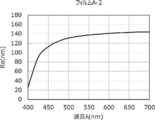
- a polyimide alignment film forming composition SE-130 (manufactured by Nissan Kagaku) was applied onto the washed glass substrate by spin coating. After the coating film was dried and sintered at 250 ° C. for 1 hour, the coating film was rubbed to form an alignment layer. The following composition A-1 was applied onto the alignment film by spin coating. The coating film formed on the orientation film was heated to 240 ° C. on a hot plate and then cooled to 200 ° C., and then, a 500 mJ / cm 2 ultraviolet ray was applied at a wavelength of 365 nm using a high pressure mercury lamp in a nitrogen atmosphere. By irradiating the film, the alignment of the liquid crystal compound was fixed and a retardation film A-1 was produced. The thickness of the retardation film A-1 is shown in Table 1.
- composition A-1 Liquid crystal compound L-1 42.00 parts by mass Liquid crystal compound L-2 42.00 parts by mass Liquid crystal compound L-3 16.00 parts by mass Polymerization initiator PI-1 0.50 parts by mass Leveling agent T- 1 0.20 parts by mass, chloroform 560.00 parts by mass ⁇
- a retardation film A-3 was produced in the same manner as in Comparative Example 1 except that the composition A-1 was changed to the following composition A-2 and the thickness was adjusted.
- Composition A-3 ⁇ Liquid crystal compound L-1 50.00 parts by mass Liquid crystal compound L-2 50.00 parts by mass Polymerization initiator PI-1 0.50 parts by mass Leveling agent T-1 0.20 parts by mass Chloroform 560.00 Mass part ⁇
- Example 1 By the same method as in Example 1 except that 14.00 parts by mass of the following dichroic dye D-1 (maximum absorption wavelength: 706 nm / 785 nm) was added to the composition A-1, and the thickness was adjusted. A retardation film A-4 was produced.
- D-1 maximum absorption wavelength: 706 nm / 785 nm
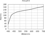
- Example 2 A retardation film A-5 was produced in the same manner as in Example 1 except that 10.00 parts by mass of the dichroic dye D-1 was added to the composition A-1 to adjust the thickness.
- Example 3 A retardation film A-6 was produced in the same manner as in Example 2 except that the thickness was adjusted.
- Example 4 A retardation film A-7 was produced in the same manner as in Example 1 except that 5.00 parts by mass of the dichroic dye D-1 was added to the composition A-1 to adjust the thickness.
- Example 5 By the same method as in Comparative Example 1 except that 0.20 parts by mass of dichroic dye G-241 (maximum absorption wavelength: 555 nm, manufactured by Nagase & Co., Ltd.) was added to Composition A-1 to adjust the thickness. A retardation film A-8 was produced.
- dichroic dye G-241 maximum absorption wavelength: 555 nm, manufactured by Nagase & Co., Ltd.
- Retardation film A-9 was prepared in the same manner as in Comparative Example 1 except that 0.70 parts by mass of dichroic dye G-241 (manufactured by Nagase & Co., Ltd.) was added to Composition A-1 to adjust the thickness. Was produced.
- Comparative Example 5 Same as Comparative Example 1 except that 0.20 parts by mass of dichroic dye M-137 (maximum absorption wavelength: 582 nm / 621 nm, manufactured by Mitsui Chemicals Fine, Inc.) was added to the composition A-1 to adjust the thickness.
- a retardation film A-10 was produced by the method of 1.
- Retardation film A was prepared in the same manner as in Comparative Example 1 except that 1.00 part by weight of dichroic dye M-137 (manufactured by Mitsui Chemicals Fine, Inc.) was added to Composition A-1 to adjust the thickness. -11 was produced.
- TD80UL manufactured by FUJIFILM Corporation
- alkali saponification treatment The surface of TD80UL (manufactured by FUJIFILM Corporation) as a support was subjected to alkali saponification treatment. Specifically, the above support is immersed in a 1.5 N sodium hydroxide aqueous solution at 55 ° C. for 2 minutes, the support taken out is washed in a water-washing bath at room temperature, and 0.1 N sulfuric acid is added at 30 ° C. Was used to neutralize. Then, the obtained support was washed again in a water-washing bath at room temperature, and further dried with hot air at 100 ° C.
- a roll-shaped polyvinyl alcohol film having a thickness of 80 ⁇ m was continuously stretched 5 times in an iodine aqueous solution, and the stretched film was dried to obtain a polarizer having a thickness of 20 ⁇ m.
- the obtained polarizer and an alkali-saponified support (TD80UL) were attached to each other to obtain a polarizing plate in which the polarizer was exposed on one side.
- polarization was performed so that the angle between the absorption axis of the polarizer and the slow axes of the retardation films A-1 to A-11 produced in Examples 1 to 5 and Comparative Examples 1 to 6 was 45 °.
- the polarizer in the plate and the coated surface of the retardation film are bonded together via an adhesive, the glass substrate is subsequently peeled off, only the retardation film is transferred onto the polarizer, and circularly polarizing plates P-1 to P -11 was produced.
- Table 1 shows various evaluation results of the retardation films and the circularly polarizing plates produced in Examples 1 to 5 and Comparative Examples 1 to 6.
- the thickness of the retardation film was measured using a reflection spectral film thickness meter FE3000 (manufactured by Otsuka Electronics Co., Ltd.).
- Re (550) represents the in-plane retardation of the retardation film at a wavelength of 550 nm.
- the “addition amount” in the “dye” column represents the amount of the dye used with respect to 100 parts by mass of the liquid crystal compound.
- the value of ⁇ xy is shown.
- Requirements 2 and 3 “A” indicates that the above requirements 2 and 3 are satisfied, and “B” indicates that at least one of the requirements 2 and 3 is not satisfied.
- Requirements 4 and 5 “A” indicates that the requirements 4 and 5 described above are satisfied, and “B” indicates that at least one of the requirements 4 and 5 is not satisfied.
Landscapes
- Physics & Mathematics (AREA)
- Optics & Photonics (AREA)
- General Physics & Mathematics (AREA)
- Chemical & Material Sciences (AREA)
- Crystallography & Structural Chemistry (AREA)
- Nonlinear Science (AREA)
- Engineering & Computer Science (AREA)
- Theoretical Computer Science (AREA)
- Polarising Elements (AREA)
- Liquid Crystal (AREA)
Abstract
本発明は、表示装置に適用した際に、外光反射が抑制され、かつ、反射光の色味づきが抑制され、さらに白表示の際の色味づきも抑制される位相差フィルム、円偏光板、および、有機エレクトロルミネッセンス表示装置を提供する。本発明の位相差フィルムは、液晶化合物を用いて形成された位相差フィルムであって、波長550nmにおける面内レタデーションが100~200nmであり、要件1および6を満たす。 要件1:Δxy<0.010 要件6:0.10<傾きS≦1.0
Description
本発明は、位相差フィルム、円偏光板、および、有機エレクトロルミネッセンス表示装置に関する。
従来から、外光反射による悪影響を抑制するために、円偏光板が有機エレクトロルミネッセンス(EL)表示装置に使用されている。円偏光板中に含まれる位相差フィルムとしては、例えば、特許文献1に記載されるような位相差フィルム(光学フィルム)が挙げられる。
一方、近年、有機EL表示装置に代表される表示装置においては、円偏光板を含む場合に、外光反射のより一層の低減が求められている。
また、円偏光板を含む表示装置においては、反射光の色味づきのより一層の抑制も求められている。
さらに、円偏光板を含む表示装置においては、白表示時の色味づきのより一層の抑制も求められている。
また、円偏光板を含む表示装置においては、反射光の色味づきのより一層の抑制も求められている。
さらに、円偏光板を含む表示装置においては、白表示時の色味づきのより一層の抑制も求められている。
本発明は、上記実情に鑑みて、表示装置に適用した際に、外光反射が抑制され、かつ、反射光の色味づきが抑制され、さらに白表示の際の色味づきも抑制される位相差フィルムを提供することも課題とする。
また、本発明は、円偏光板、および、有機エレクトロルミネッセンス表示装置を提供することも課題とする。
また、本発明は、円偏光板、および、有機エレクトロルミネッセンス表示装置を提供することも課題とする。
本発明者らは、従来技術の問題点について鋭意検討した結果、所定の要件を満たす位相差フィルムを用いることにより、上記課題を解決できることを見出した。
すなわち、以下の構成により上記課題を解決できることを見出した。
すなわち、以下の構成により上記課題を解決できることを見出した。
(1) 少なくとも液晶化合物を用いて形成された位相差フィルムであって、
波長550nmにおける面内レタデーションが100~200nmであり、
CIExy色度図上において、位相差フィルムに対して標準光源D65の光を入射させて得られる透過光の色度と、標準光源D65の色度との差であるΔxyが後述する要件1を満たし、
位相差フィルムに入射する測定光の波長を横軸に、波長450~600nmの範囲における25nm毎の測定光の波長における位相差フィルムの面内レタデーションを縦軸にプロットしたグラフにおいて、隣接する2つのプロット点を結ぶ直線の傾きSが、いずれも後述する要件6を満たす、位相差フィルム。
(2) 位相差フィルムに入射する測定光の波長を横軸に、波長450~650nmの範囲における25nm毎の測定光の波長における位相差フィルムの面内レタデーションを縦軸にプロットしたグラフにおいて、隣接する2つのプロット点を結ぶ直線の傾きSが、いずれも後述する要件7を満たす、(1)に記載の位相差フィルム。
(3) グラフにおいて、測定光が波長550nmであるプロット点と、測定光が波長575nmであるプロット点とを結んだ直線の傾きS(550)が後述する要件8を満たす、(1)または(2)に記載の位相差フィルム。
(4) グラフにおいて、測定光が波長625nmであるプロット点と、測定光が波長650nmであるプロット点とを結んだ直線の傾きS(625)が後述する要件9を満たす、(1)~(3)のいずれかに記載の位相差フィルム。
(5) 少なくとも液晶化合物を用いて形成された位相差フィルムであって、
波長550nmにおける面内レタデーションが100~200nmであり、
CIExy色度図上において、位相差フィルムに対して標準光源D65の光を入射させて得られる透過光の色度と、標準光源D65の色度との差であるΔxyが後述する要件1を満たし、
位相差フィルムに入射する測定光の波長を横軸に、測定波長550nmにおける位相差フィルムの面内レタデーションを1.0として規格化した測定光の各波長における面内レタデーションを縦軸にプロットしたグラフにおいて、波長450~550nmの範囲内の波長λ1における位相差フィルムの面内レタデーションRe(λ1)が後述する要件10を満たし、波長550~650nmの範囲内の波長λ2における位相差フィルムの面内レタデーションRe(λ2)が後述する要件11を満たす、位相差フィルム。
(6) 液晶化合物が逆波長分散性を示す、(1)~(5)のいずれかに記載の位相差フィルム。
(7) 偏光子と、(1)~(6)のいずれかに記載の位相差フィルムとを含む、円偏光板。
(8) 有機エレクトロルミネッセンス表示パネルと、有機エレクトロルミネッセンス表示パネル上に配置された(7)に記載の円偏光板と、を含む有機エレクトロルミネッセンス表示装置。
波長550nmにおける面内レタデーションが100~200nmであり、
CIExy色度図上において、位相差フィルムに対して標準光源D65の光を入射させて得られる透過光の色度と、標準光源D65の色度との差であるΔxyが後述する要件1を満たし、
位相差フィルムに入射する測定光の波長を横軸に、波長450~600nmの範囲における25nm毎の測定光の波長における位相差フィルムの面内レタデーションを縦軸にプロットしたグラフにおいて、隣接する2つのプロット点を結ぶ直線の傾きSが、いずれも後述する要件6を満たす、位相差フィルム。
(2) 位相差フィルムに入射する測定光の波長を横軸に、波長450~650nmの範囲における25nm毎の測定光の波長における位相差フィルムの面内レタデーションを縦軸にプロットしたグラフにおいて、隣接する2つのプロット点を結ぶ直線の傾きSが、いずれも後述する要件7を満たす、(1)に記載の位相差フィルム。
(3) グラフにおいて、測定光が波長550nmであるプロット点と、測定光が波長575nmであるプロット点とを結んだ直線の傾きS(550)が後述する要件8を満たす、(1)または(2)に記載の位相差フィルム。
(4) グラフにおいて、測定光が波長625nmであるプロット点と、測定光が波長650nmであるプロット点とを結んだ直線の傾きS(625)が後述する要件9を満たす、(1)~(3)のいずれかに記載の位相差フィルム。
(5) 少なくとも液晶化合物を用いて形成された位相差フィルムであって、
波長550nmにおける面内レタデーションが100~200nmであり、
CIExy色度図上において、位相差フィルムに対して標準光源D65の光を入射させて得られる透過光の色度と、標準光源D65の色度との差であるΔxyが後述する要件1を満たし、
位相差フィルムに入射する測定光の波長を横軸に、測定波長550nmにおける位相差フィルムの面内レタデーションを1.0として規格化した測定光の各波長における面内レタデーションを縦軸にプロットしたグラフにおいて、波長450~550nmの範囲内の波長λ1における位相差フィルムの面内レタデーションRe(λ1)が後述する要件10を満たし、波長550~650nmの範囲内の波長λ2における位相差フィルムの面内レタデーションRe(λ2)が後述する要件11を満たす、位相差フィルム。
(6) 液晶化合物が逆波長分散性を示す、(1)~(5)のいずれかに記載の位相差フィルム。
(7) 偏光子と、(1)~(6)のいずれかに記載の位相差フィルムとを含む、円偏光板。
(8) 有機エレクトロルミネッセンス表示パネルと、有機エレクトロルミネッセンス表示パネル上に配置された(7)に記載の円偏光板と、を含む有機エレクトロルミネッセンス表示装置。
本発明によれば、表示装置に適用した際に、外光反射が抑制され、かつ、反射光の色味づきが抑制され、さらに白表示の際の色味づきも抑制される位相差フィルムを提供できる。
また、本発明によれば、円偏光板、および、有機エレクトロルミネッセンス表示装置を提供できる。
また、本発明によれば、円偏光板、および、有機エレクトロルミネッセンス表示装置を提供できる。
以下、本発明について詳細に説明する。なお、本明細書において「~」を用いて表される数値範囲は、「~」の前後に記載される数値を下限値および上限値として含む範囲を意味する。まず、本明細書で用いられる用語について説明する。
本発明において、Re(λ)およびRth(λ)は各々、波長λにおける面内レタデーションおよび厚み方向のレタデーションを表す。例えば、Re(450)は、波長450nmにおける面内レタデーションを表す。特に記載がないときは、波長λは、550nmとする。
本発明において、Re(λ)およびRth(λ)はAxoScan OPMF-1(オプトサイエンス社製)において、波長λで測定した値である。AxoScanにて平均屈折率((nx+ny+nz)/3)と膜厚(d(μm))を入力することにより、
遅相軸方向(°)
Re(λ)=R0(λ)
Rth(λ)=((nx+ny)/2-nz)×d
が算出される。
なお、R0(λ)は、AxoScan OPMF-1で算出される数値として表示されるものであるが、Re(λ)を意味している。
本発明において、Re(λ)およびRth(λ)はAxoScan OPMF-1(オプトサイエンス社製)において、波長λで測定した値である。AxoScanにて平均屈折率((nx+ny+nz)/3)と膜厚(d(μm))を入力することにより、
遅相軸方向(°)
Re(λ)=R0(λ)
Rth(λ)=((nx+ny)/2-nz)×d
が算出される。
なお、R0(λ)は、AxoScan OPMF-1で算出される数値として表示されるものであるが、Re(λ)を意味している。
本明細書において、屈折率nx、ny、および、nzは、アッベ屈折計(NAR-4T、アタゴ(株)製)を使用し、光源にナトリウムランプ(λ=589nm)を用いて測定する。また、波長依存性を測定する場合は、多波長アッベ屈折計DR-M2(アタゴ(株)製)にて、干渉フィルタとの組み合わせで測定できる。
また、ポリマーハンドブック(JOHN WILEY&SONS,INC)、および、各種光学フィルムのカタログの値を使用できる。主な光学フィルムの平均屈折率の値を以下に例示する:セルロースアシレート(1.48)、シクロオレフィンポリマー(1.52)、ポリカーボネート(1.59)、ポリメチルメタクリレート(1.49)、および、ポリスチレン(1.59)。
また、本明細書において、Nzファクターとは、Nz=(nx-nz)/(nx-ny)で与えられる値である。
また、ポリマーハンドブック(JOHN WILEY&SONS,INC)、および、各種光学フィルムのカタログの値を使用できる。主な光学フィルムの平均屈折率の値を以下に例示する:セルロースアシレート(1.48)、シクロオレフィンポリマー(1.52)、ポリカーボネート(1.59)、ポリメチルメタクリレート(1.49)、および、ポリスチレン(1.59)。
また、本明細書において、Nzファクターとは、Nz=(nx-nz)/(nx-ny)で与えられる値である。
なお、本明細書では、「可視光」とは、400~700nmのことをいう。
また、本明細書において、角度(例えば「90°」などの角度)、および、その関係(例えば「直交」、「平行」、および「45°で交差」など)については、本発明が属する技術分野において許容される誤差の範囲を含むものとする。例えば、厳密な角度±10°の範囲内であることなどを意味し、厳密な角度との誤差は、±5°の範囲内であることが好ましく、±3°の範囲内であることがより好ましい。
また、本明細書において、角度(例えば「90°」などの角度)、および、その関係(例えば「直交」、「平行」、および「45°で交差」など)については、本発明が属する技術分野において許容される誤差の範囲を含むものとする。例えば、厳密な角度±10°の範囲内であることなどを意味し、厳密な角度との誤差は、±5°の範囲内であることが好ましく、±3°の範囲内であることがより好ましい。
本明細書において、偏光子の「吸収軸」は、吸光度の最も高い方向を意味する。「透過軸」は、「吸収軸」と90°の角度をなす方向を意味する。
本明細書において表記される2価の基(例えば、-O-CO-)の結合方向は特に制限されず、例えば、後述する式(I)中のD1が-O-CO-である場合、Ar側に結合している位置を*1、G1側に結合している位置を*2とすると、D1は*1-O-CO-*2であってもよく、*1-CO-O-*2であってもよい。
以下に、本発明の位相差フィルム、円偏光板、および、有機エレクトロルミネッセンス表示装置(有機EL表示装置)について図面を参照して説明する。
なお、以下では、位相差フィルム、円偏光板、および、有機EL表示装置の順に説明する。なお、位相差フィルムに関しては、第1実施形態および第2実施形態に分けて説明する。
なお、以下では、位相差フィルム、円偏光板、および、有機EL表示装置の順に説明する。なお、位相差フィルムに関しては、第1実施形態および第2実施形態に分けて説明する。
<位相差フィルム>
(第1実施形態)
位相差フィルムの第1実施形態(以後、「第1位相差フィルム」ともいう。)は、液晶化合物を用いて形成された位相差フィルムであって、波長550nmにおける面内レタデーションが100~200nmであり、後述する要件1~要件3を満たす、位相差フィルムである。
また、後述するように、位相差フィルムの第1実施形態は、後述する要件1、10および11を満たすことが好ましい。
以下、第1位相差フィルムの構成について詳述する。
(第1実施形態)
位相差フィルムの第1実施形態(以後、「第1位相差フィルム」ともいう。)は、液晶化合物を用いて形成された位相差フィルムであって、波長550nmにおける面内レタデーションが100~200nmであり、後述する要件1~要件3を満たす、位相差フィルムである。
また、後述するように、位相差フィルムの第1実施形態は、後述する要件1、10および11を満たすことが好ましい。
以下、第1位相差フィルムの構成について詳述する。
第1位相差フィルムの波長550nmにおける面内レタデーションRe(550)は、100~200nmであり、外光反射がより抑制される点、反射光の色味づきがより抑制される点、および、白表示の際の色味づきがより抑制される点の少なくとも1つの点(以後、「本発明の効果がより優れる点」ともいう)で、120~160nmがより好ましく、130~150nmがさらに好ましく、130~140nmが特に好ましい。
第1位相差フィルムの波長550nmにおける厚み方向のレタデーションRth(550)は特に制限されないが、50~100nmが好ましく、60~80nmがより好ましく、65~75nmがさらに好ましい。
第1位相差フィルムの波長550nmにおける厚み方向のレタデーションRth(550)は特に制限されないが、50~100nmが好ましく、60~80nmがより好ましく、65~75nmがさらに好ましい。
第1位相差フィルムは、逆波長分散性を示すことが好ましい。なお、上記逆波長分散性は、可視光域において示されることが好ましい。
第1位相差フィルムが逆波長分散性を示すとは、第1位相差フィルムの面内レタデーションが、測定波長が大きくなるにつれて大きくなることを意味する。言い換えると、後述するRe(450)、Re(550)、および、Re(650)は、以下の関係Xを満たす。
関係X:Re(450)<Re(550)<Re(650)
第1位相差フィルムが逆波長分散性を示すとは、第1位相差フィルムの面内レタデーションが、測定波長が大きくなるにつれて大きくなることを意味する。言い換えると、後述するRe(450)、Re(550)、および、Re(650)は、以下の関係Xを満たす。
関係X:Re(450)<Re(550)<Re(650)
第1位相差フィルムのRe(450)/Re(550)は、0.75~0.99であることが好ましく、0.80~0.95であることがより好ましい。上記Re(450)/Re(550)は、第1位相差フィルムの波長550nmにおける面内レタデーションであるRe(550)に対する、第1位相差フィルムの波長450nmにおける面内レタデーションであるRe(450)の比を表す。
また、第1位相差フィルムのRe(650)/Re(550)は、1.03~1.20であることが好ましく、1.08~1.15であることがより好ましい。上記Re(650)/Re(550)は、第1位相差フィルムの波長550nmにおける面内レタデーションであるRe(550)に対する、第1位相差フィルムの波長650nmにおける面内レタデーションであるRe(650)の比を表す。
また、第1位相差フィルムのRe(650)/Re(550)は、1.03~1.20であることが好ましく、1.08~1.15であることがより好ましい。上記Re(650)/Re(550)は、第1位相差フィルムの波長550nmにおける面内レタデーションであるRe(550)に対する、第1位相差フィルムの波長650nmにおける面内レタデーションであるRe(650)の比を表す。
CIExy色度図上において、第1位相差フィルムに対して標準光源D65の光を入射させて得られる透過光の色度と、標準光源D65の色度(標準光源D65の光の色度)との差であるΔxyが要件1を満たす。
要件1:Δxy<0.010
ただし、Δxyは、以下式より算出される。
式:Δxy=((x-x0)2+(y-y0)2)1/2
xおよびyは第1位相差フィルムの透過光のCIExy色度図上の色度座標を表し、x0およびy0は標準光源D65(標準光源D65の光)のCIExy色度図上の色度座標を表す。
なかでも、反射光の色味づきがより抑制される点、および、白表示の際の色味づきがより抑制される点で、上記Δxyは、0.008以下が好ましい。Δxyの下限は特に制限されないが、0.001以上の場合が多い。
上記色度の測定方法は、以下の通りである。
分光光度計(UV-3150 島津製作所製)を用い、波長380~780nmの範囲で10nmおきにフィルムの透過率を測定し、得られた値を標準光源D65の分光分布と掛け合わせ、各波長における透過光強度分布を算出する。得られた透過光強度にCIEスペクトル三刺激値(例えば、「色の科学 その心理と生理と物理 金子隆芳著」参照)を乗じて全波長で足し合わせた値をそれぞれX、Y、Z、さらにx+y+z=1となるように規格化した値(x、y)を透過光の色度とする。なお、上記規格化の方法としては、x=X/(X+Y+Z)、y=Y/(X+Y+Z)、および、z=Z/(X+Y+Z)を求める。そして、得られた透過光の色度(x,y)と、標準光源D65の色度(x0,y0)=(0.31271、0.32902)との差であるΔxyを上述した式に沿って、計算する。
なお、上記透過光の色度の算出は、標準光源D65と同様の分光分布を有する光を照射したと仮定したシミュレーションによって行ってもよい。
要件1:Δxy<0.010
ただし、Δxyは、以下式より算出される。
式:Δxy=((x-x0)2+(y-y0)2)1/2
xおよびyは第1位相差フィルムの透過光のCIExy色度図上の色度座標を表し、x0およびy0は標準光源D65(標準光源D65の光)のCIExy色度図上の色度座標を表す。
なかでも、反射光の色味づきがより抑制される点、および、白表示の際の色味づきがより抑制される点で、上記Δxyは、0.008以下が好ましい。Δxyの下限は特に制限されないが、0.001以上の場合が多い。
上記色度の測定方法は、以下の通りである。
分光光度計(UV-3150 島津製作所製)を用い、波長380~780nmの範囲で10nmおきにフィルムの透過率を測定し、得られた値を標準光源D65の分光分布と掛け合わせ、各波長における透過光強度分布を算出する。得られた透過光強度にCIEスペクトル三刺激値(例えば、「色の科学 その心理と生理と物理 金子隆芳著」参照)を乗じて全波長で足し合わせた値をそれぞれX、Y、Z、さらにx+y+z=1となるように規格化した値(x、y)を透過光の色度とする。なお、上記規格化の方法としては、x=X/(X+Y+Z)、y=Y/(X+Y+Z)、および、z=Z/(X+Y+Z)を求める。そして、得られた透過光の色度(x,y)と、標準光源D65の色度(x0,y0)=(0.31271、0.32902)との差であるΔxyを上述した式に沿って、計算する。
なお、上記透過光の色度の算出は、標準光源D65と同様の分光分布を有する光を照射したと仮定したシミュレーションによって行ってもよい。
第1位相差フィルムに入射する測定光の波長を横軸に、測定波長550nmにおける第1位相差フィルムの面内レタデーションを1.0として規格化した測定光の各波長における面内レタデーションを縦軸にプロットしたグラフにおいて、波長450~550nmの範囲内の波長λ1における第1位相差フィルムの面内レタデーションRe(λ1)が以下の要件2を満たし、波長550~650nmの範囲内の波長λ2における第1位相差フィルムの面内レタデーションRe(λ2)が以下の要件3を満たす。
要件2:0.0027×λ1-0.5≦Re(λ1)/Re(550)≦0.0009×λ1+0.5
要件3:0.0009×λ2+0.5≦Re(λ2)/Re(550)≦0.0027×λ2-0.5
上記要件2および3について、図面を用いて詳細に説明する。
まず、図1に示すグラフ(直交座標)においては、横軸が、第1位相差フィルムに入射する測定光の波長を示す。縦軸は、測定波長550nmにおける第1位相差フィルムの面内レタデーションを1.0として規格化した測定光の各波長における面内レタデーションを示す。つまり、各波長における第1位相差フィルムの面内レタデーションをRe(λ)、測定波長550nmにおける第1位相差フィルムの面内レタデーションRe(550)とした場合、縦軸はRe(λ)/Re(550)を表す。
次に、このグラフ中に、測定光の各波長における第1位相差フィルムの面内レタデーションをそれぞれプロットする。なお、図1においては、太線で示す曲線が、第1位相差フィルムの面内レタデーションをプロットして形成される線(プロットした点をつないで形成される線)に該当する。
図1中の破線で表される2つの直線は、以下の式で表される。
式A:Re(λ)/Re(550)=0.0027×λ-0.5
式B:Re(λ)/Re(550)=0.0009×λ+0.5
要件2は、波長450~550nmの範囲内の波長λ1における第1位相差フィルムの面内レタデーションRe(λ1)が式Aで表される直線と式Bで表される直線との間に位置することを表す。つまり、図1において、波長450~550nmにおける太線で示す曲線が、式Aで表される直線と式Bで表される直線との間に位置することを表す。
要件3は、波長550~650nmの範囲内の波長λ2における第1位相差フィルムの面内レタデーションRe(λ2)が式Aで表される直線と式Bで表される直線との間に位置することを表す。つまり、図1において、波長550~650nmにおける太線で示す曲線が、式Aで表される直線と式Bで表される直線との間に位置することを表す。
各波長(450~650nm)における第1位相差フィルムの面内レタデーションが要件2および3を満たすことにより、本発明の効果が得られる。
要件2:0.0027×λ1-0.5≦Re(λ1)/Re(550)≦0.0009×λ1+0.5
要件3:0.0009×λ2+0.5≦Re(λ2)/Re(550)≦0.0027×λ2-0.5
上記要件2および3について、図面を用いて詳細に説明する。
まず、図1に示すグラフ(直交座標)においては、横軸が、第1位相差フィルムに入射する測定光の波長を示す。縦軸は、測定波長550nmにおける第1位相差フィルムの面内レタデーションを1.0として規格化した測定光の各波長における面内レタデーションを示す。つまり、各波長における第1位相差フィルムの面内レタデーションをRe(λ)、測定波長550nmにおける第1位相差フィルムの面内レタデーションRe(550)とした場合、縦軸はRe(λ)/Re(550)を表す。
次に、このグラフ中に、測定光の各波長における第1位相差フィルムの面内レタデーションをそれぞれプロットする。なお、図1においては、太線で示す曲線が、第1位相差フィルムの面内レタデーションをプロットして形成される線(プロットした点をつないで形成される線)に該当する。
図1中の破線で表される2つの直線は、以下の式で表される。
式A:Re(λ)/Re(550)=0.0027×λ-0.5
式B:Re(λ)/Re(550)=0.0009×λ+0.5
要件2は、波長450~550nmの範囲内の波長λ1における第1位相差フィルムの面内レタデーションRe(λ1)が式Aで表される直線と式Bで表される直線との間に位置することを表す。つまり、図1において、波長450~550nmにおける太線で示す曲線が、式Aで表される直線と式Bで表される直線との間に位置することを表す。
要件3は、波長550~650nmの範囲内の波長λ2における第1位相差フィルムの面内レタデーションRe(λ2)が式Aで表される直線と式Bで表される直線との間に位置することを表す。つまり、図1において、波長550~650nmにおける太線で示す曲線が、式Aで表される直線と式Bで表される直線との間に位置することを表す。
各波長(450~650nm)における第1位相差フィルムの面内レタデーションが要件2および3を満たすことにより、本発明の効果が得られる。
なかでも、本発明の効果がより優れる点で、上述したグラフにおいて、波長450~550nmの範囲内の波長λ1における第1位相差フィルムの面内レタデーションRe(λ1)が以下の要件4を満たし、波長550~650nmの範囲内の波長λ2における第1位相差フィルムの面内レタデーションRe(λ2)が以下の要件5を満たすことが好ましい。
要件4:0.0023×λ1-0.25≦Re(λ1)/Re(550)≦0.0014×λ1+0.25
要件5:0.0014×λ2+0.25≦Re(λ2)/Re(550)≦0.0023×λ2-0.25
図1中の実線で表される2つの直線は、以下の式で表される。
式C:Re(λ)/Re(550)=0.0023×λ-0.25
式D:Re(λ)/Re(550)=0.0014×λ+0.25
要件4は、波長450~550nmの範囲内の波長λ1における第1位相差フィルムの面内レタデーションRe(λ1)が式Cで表される直線と式Dで表される直線との間に位置することを表す。つまり、図1において、波長450~550nmにおける太線で示す曲線が、式Cで表される直線と式Dで表される直線との間に位置することを表す。
要件5は、波長550~650nmの範囲内の波長λ2における第1位相差フィルムの面内レタデーションRe(λ2)が式Cで表される直線と式Dで表される直線との間に位置することを表す。つまり、図1において、波長550~650nmにおける太線で示す曲線が、式Cと式Dとの間に位置することを表す。
要件4:0.0023×λ1-0.25≦Re(λ1)/Re(550)≦0.0014×λ1+0.25
要件5:0.0014×λ2+0.25≦Re(λ2)/Re(550)≦0.0023×λ2-0.25
図1中の実線で表される2つの直線は、以下の式で表される。
式C:Re(λ)/Re(550)=0.0023×λ-0.25
式D:Re(λ)/Re(550)=0.0014×λ+0.25
要件4は、波長450~550nmの範囲内の波長λ1における第1位相差フィルムの面内レタデーションRe(λ1)が式Cで表される直線と式Dで表される直線との間に位置することを表す。つまり、図1において、波長450~550nmにおける太線で示す曲線が、式Cで表される直線と式Dで表される直線との間に位置することを表す。
要件5は、波長550~650nmの範囲内の波長λ2における第1位相差フィルムの面内レタデーションRe(λ2)が式Cで表される直線と式Dで表される直線との間に位置することを表す。つまり、図1において、波長550~650nmにおける太線で示す曲線が、式Cと式Dとの間に位置することを表す。
また、本発明の効果がより優れる点で、上述したグラフにおいて、波長450~550nmの範囲内の波長λ1における第1位相差フィルムの面内レタデーションRe(λ1)が以下の要件10を満たし、波長550~650nmの範囲内の波長λ2における第1位相差フィルムの面内レタデーションRe(λ2)が以下の要件11を満たすことも好ましい。
要件10:0.0027×λ1-0.5≦Re(λ1)/Re(550)≦0.0014×λ1+0.25
要件11:0.0009×λ2+0.5≦Re(λ2)/Re(550)≦0.0023×λ2-0.25
要件10は、波長450~550nmの範囲内の波長λ1における第1位相差フィルムの面内レタデーションRe(λ1)が式Aで表される直線と式Dで表される直線との間に位置することを表す。つまり、図1において、波長450~550nmにおける太線で示す曲線が、式Aで表される直線と式Dで表される直線との間に位置することを表す。
要件11は、波長550~650nmの範囲内の波長λ2における第1位相差フィルムの面内レタデーションRe(λ2)が式Bで表される直線と式Cで表される直線との間に位置することを表す。つまり、図1において、波長550~650nmにおける太線で示す曲線が、式Bと式Cとの間に位置することを表す。
要件10:0.0027×λ1-0.5≦Re(λ1)/Re(550)≦0.0014×λ1+0.25
要件11:0.0009×λ2+0.5≦Re(λ2)/Re(550)≦0.0023×λ2-0.25
要件10は、波長450~550nmの範囲内の波長λ1における第1位相差フィルムの面内レタデーションRe(λ1)が式Aで表される直線と式Dで表される直線との間に位置することを表す。つまり、図1において、波長450~550nmにおける太線で示す曲線が、式Aで表される直線と式Dで表される直線との間に位置することを表す。
要件11は、波長550~650nmの範囲内の波長λ2における第1位相差フィルムの面内レタデーションRe(λ2)が式Bで表される直線と式Cで表される直線との間に位置することを表す。つまり、図1において、波長550~650nmにおける太線で示す曲線が、式Bと式Cとの間に位置することを表す。
また、本発明の効果がより優れる点で、波長450~550nmの範囲内の波長λ1における第1位相差フィルムの面内レタデーションRe(λ1)が以下の要件12を満たし、波長550~650nmの範囲内の波長λ2における第1位相差フィルムの面内レタデーションRe(λ2)が以下の要件13を満たすことも好ましい。
要件12:0.0027×λ1-0.485≦Re(λ1)/Re(550)≦0.0009×λ1+0.505
要件13:0.0009×λ2+0.505≦Re(λ2)/Re(550)≦0.0027×λ2-0.485
さらに、本発明の効果がより優れる点で、波長450~550nmの範囲内の波長λ1における第1位相差フィルムの面内レタデーションRe(λ1)が以下の要件14を満たし、波長550~650nmの範囲内の波長λ2における第1位相差フィルムの面内レタデーションRe(λ2)が以下の要件15を満たすことも好ましい。
要件14:0.0023×λ1-0.265≦Re(λ1)/Re(550)≦0.0014×λ1+0.23
要件15:0.0014×λ2+0.23≦Re(λ2)/Re(550)≦0.0023×λ2-0.265
要件12:0.0027×λ1-0.485≦Re(λ1)/Re(550)≦0.0009×λ1+0.505
要件13:0.0009×λ2+0.505≦Re(λ2)/Re(550)≦0.0027×λ2-0.485
さらに、本発明の効果がより優れる点で、波長450~550nmの範囲内の波長λ1における第1位相差フィルムの面内レタデーションRe(λ1)が以下の要件14を満たし、波長550~650nmの範囲内の波長λ2における第1位相差フィルムの面内レタデーションRe(λ2)が以下の要件15を満たすことも好ましい。
要件14:0.0023×λ1-0.265≦Re(λ1)/Re(550)≦0.0014×λ1+0.23
要件15:0.0014×λ2+0.23≦Re(λ2)/Re(550)≦0.0023×λ2-0.265
また、本発明においては、波長450~500nmの範囲内の波長λ1における第1位相差フィルムの面内レタデーションRe(λ1)が上記要件2を満たし、波長600~650nmの範囲内の波長λ2における第1位相差フィルムの面内レタデーションRe(λ2)が上記要件3を満たすことも好ましい。
第1位相差フィルムは、本発明の効果がより優れる点で、後述する要件6~9の少なくとも1つを満たしていることが好ましい。
第1位相差フィルムの厚みは特に制限されず、面内レタデーションが所定の範囲となるように調整されるが、薄型化の点から、10μm以下が好ましく、0.5~8.0μmがより好ましく、0.5~6.0μmがさらに好ましい。
なお、本明細書において、第1位相差フィルムの厚みとは、第1位相差フィルムの平均厚みを意図する。上記平均厚みは、第1位相差フィルムの任意の5点以上の厚みを測定して、それらを算術平均して求める。
なお、本明細書において、第1位相差フィルムの厚みとは、第1位相差フィルムの平均厚みを意図する。上記平均厚みは、第1位相差フィルムの任意の5点以上の厚みを測定して、それらを算術平均して求める。
(第2実施形態)
位相差フィルムの第2実施形態(以後、「第2位相差フィルム」ともいう。)は、液晶化合物を用いて形成された位相差フィルムであって、波長550nmにおける面内レタデーションが100~200nmであり、後述する要件1および要件6を満たす、位相差フィルムである。
以下、第2位相差フィルムの構成について詳述する。
位相差フィルムの第2実施形態(以後、「第2位相差フィルム」ともいう。)は、液晶化合物を用いて形成された位相差フィルムであって、波長550nmにおける面内レタデーションが100~200nmであり、後述する要件1および要件6を満たす、位相差フィルムである。
以下、第2位相差フィルムの構成について詳述する。
第2位相差フィルムの波長550nmにおける面内レタデーションRe(550)は、100~200nmであり、本発明の効果がより優れる点で、120~160nmがより好ましく、130~150nmがさらに好ましく、130~140nmが特に好ましい。
第2位相差フィルムの波長550nmにおける厚み方向のレタデーションRth(550)は特に制限されないが、50~100nmが好ましく、60~80nmがより好ましく、65~75nmがさらに好ましい。
第2位相差フィルムの波長550nmにおける厚み方向のレタデーションRth(550)は特に制限されないが、50~100nmが好ましく、60~80nmがより好ましく、65~75nmがさらに好ましい。
第2位相差フィルムは、逆波長分散性を示すことが好ましい。なお、上記逆波長分散性は、可視光域において示されることが好ましい。
第2位相差フィルムが逆波長分散性を示すとは、第2位相差フィルムの面内レタデーションが、測定波長が大きくなるにつれて大きくなることを意味する。言い換えると、後述するRe(450)、Re(550)、および、Re(650)は、以下の関係Xを満たす。
関係X:Re(450)<Re(550)<Re(650)
第2位相差フィルムが逆波長分散性を示すとは、第2位相差フィルムの面内レタデーションが、測定波長が大きくなるにつれて大きくなることを意味する。言い換えると、後述するRe(450)、Re(550)、および、Re(650)は、以下の関係Xを満たす。
関係X:Re(450)<Re(550)<Re(650)
第2位相差フィルムのRe(450)/Re(550)は、0.75~0.99であることが好ましく、0.80~0.95であることがより好ましい。上記Re(450)/Re(550)は、第2位相差フィルムの波長550nmにおける面内レタデーションであるRe(550)に対する、第2位相差フィルムの波長450nmにおける面内レタデーションであるRe(450)の比を表す。
また、第2位相差フィルムのRe(650)/Re(550)は、1.03~1.20であることが好ましく、1.08~1.15であることがより好ましい。上記Re(650)/Re(550)は、第2位相差フィルムの波長550nmにおける面内レタデーションであるRe(550)に対する、第1位相差フィルムの波長650nmにおける面内レタデーションであるRe(650)の比を表す。
また、第2位相差フィルムのRe(650)/Re(550)は、1.03~1.20であることが好ましく、1.08~1.15であることがより好ましい。上記Re(650)/Re(550)は、第2位相差フィルムの波長550nmにおける面内レタデーションであるRe(550)に対する、第1位相差フィルムの波長650nmにおける面内レタデーションであるRe(650)の比を表す。
CIExy色度図上において、第2位相差フィルムに対して標準光源D65の光を入射させて得られる透過光の色度と、標準光源D65(標準光源D65の光)の色度との差であるΔxyが要件1を満たす。
要件1:Δxy<0.010
ただし、Δxyは、以下式より算出される。
式:Δxy=((x-x0)2+(y-y0)2)1/2
xおよびyは第2位相差フィルムの透過光のCIExy色度図上の色度座標を表し、x0およびy0は標準光源D65(標準光源D65の光)のCIExy色度図上の色度座標を表す。
なかでも、反射色味がより低減される点で、上記Δxyは、0.008以下が好ましい。Δxyの下限は特に制限されないが、0.001以上の場合が多い。
上記色度の測定方法は、以下の通りである。
分光光度計(UV-3150 島津製作所製)を用い、波長380~780nmの範囲で10nmおきにフィルムの透過率を測定し、得られた値を標準光源D65の分光分布と掛け合わせ、各波長における透過光強度分布を算出する。得られた透過光強度にCIEスペクトル三刺激値(例えば、「色の科学 その心理と生理と物理 金子隆芳著」参照)を乗じて全波長で足し合わせた値をそれぞれX、Y、Z、さらにx+y+z=1となるように規格化した値(x、y)を透過光の色度とする。なお、上記規格化の方法としては、x=X/(X+Y+Z)、y=Y/(X+Y+Z)、および、z=Z/(X+Y+Z)を求める。そして、得られた透過光の色度(x,y)と、標準光源D65の色度(x0,y0)=(0.31271、0.32902)との差であるΔxyを上述した式に沿って、計算する。
なお、上記透過光の色度の算出は、標準光源D65と同様の分光分布を有する光を照射したと仮定したシミュレーションによって行ってもよい。
要件1:Δxy<0.010
ただし、Δxyは、以下式より算出される。
式:Δxy=((x-x0)2+(y-y0)2)1/2
xおよびyは第2位相差フィルムの透過光のCIExy色度図上の色度座標を表し、x0およびy0は標準光源D65(標準光源D65の光)のCIExy色度図上の色度座標を表す。
なかでも、反射色味がより低減される点で、上記Δxyは、0.008以下が好ましい。Δxyの下限は特に制限されないが、0.001以上の場合が多い。
上記色度の測定方法は、以下の通りである。
分光光度計(UV-3150 島津製作所製)を用い、波長380~780nmの範囲で10nmおきにフィルムの透過率を測定し、得られた値を標準光源D65の分光分布と掛け合わせ、各波長における透過光強度分布を算出する。得られた透過光強度にCIEスペクトル三刺激値(例えば、「色の科学 その心理と生理と物理 金子隆芳著」参照)を乗じて全波長で足し合わせた値をそれぞれX、Y、Z、さらにx+y+z=1となるように規格化した値(x、y)を透過光の色度とする。なお、上記規格化の方法としては、x=X/(X+Y+Z)、y=Y/(X+Y+Z)、および、z=Z/(X+Y+Z)を求める。そして、得られた透過光の色度(x,y)と、標準光源D65の色度(x0,y0)=(0.31271、0.32902)との差であるΔxyを上述した式に沿って、計算する。
なお、上記透過光の色度の算出は、標準光源D65と同様の分光分布を有する光を照射したと仮定したシミュレーションによって行ってもよい。
第2位相差フィルムに入射する測定光の波長を横軸に、波長450~600nmの範囲における25nm毎の測定光の波長における第2位相差フィルムの面内レタデーションを縦軸にプロットしたグラフにおいて、隣接する2つのプロット点を結ぶ直線の傾きSが、いずれも要件6を満たす。
要件6:0.10<傾きS≦1.0
上記要件6について、図面を用いて詳細に説明する。
まず、図2に示すグラフ(直交座標)においては、横軸が、第2位相差フィルムに入射する測定光の波長を示す。縦軸は、測定光の波長における第2位相差フィルムの面内レタデーション(nm)を示す。
次に、このグラフ中に、測定光の各波長における第2位相差フィルムの面内レタデーションをそれぞれプロットする。なお、測定に際しては、波長450~600nmの範囲における25nm毎の測定光にて実施する。つまり、図2に示すように、波長450nm、波長475nm、波長500nm、波長525nm、波長550nm、波長575nm、および、波長600nmの測定光における面内レタデーションをそれぞれ求めて、グラフ上にプロットする。
次に、隣接する2つのプロット点を直線で結ぶ。より具体的には、図2に示すように、波長450nmでのプロット点と波長475nmでのプロット点とを直線(直線1)で結び、波長475nmでのプロット点と波長500nmでのプロット点とを直線(直線2)で結び、波長500nmでのプロット点と波長525nmでのプロット点とを直線(直線3)で結び、波長525nmでのプロット点と波長550nmでのプロット点とを直線(直線4)で結び、波長550nmでのプロット点と波長575nmでのプロット点とを直線(直線5)で結び、波長575nmでのプロット点と波長600nmでのプロット点とを直線(直線6)で結ぶ。
次に、得られた各直線(直線1~6)の傾きSをそれぞれ算出する。得られたすべての傾きS(直線1~6のそれぞれの傾きS)が、0.10超1.0以下であれば、要件6を満たす。
なかでも、本発明の効果がより優れる点から、第2位相差フィルムに入射する測定光の波長を横軸に、波長450~650nmの範囲における25nm毎の測定光の波長における第2位相差フィルムの面内レタデーションを縦軸にプロットしたグラフにおいて、隣接する2つのプロット点を結ぶ直線の傾きSが、いずれも要件7を満たすことが好ましい。
要件7:0.10<傾きS≦1.0
要件7の要件を満たすか否か判断するためには、波長450nm、波長475nm、波長500nm、波長525nm、波長550nm、波長575nm、波長600nm、波長625nm、および、波長650nmの測定光における面内レタデーションをそれぞれ求めて、グラフ上にプロットする。そして、直線1~6のそれぞれの傾き、波長600nmでのプロット点と波長625nmでのプロット点とを直線(直線7)の傾き、および、波長625nmでのプロット点と波長650nmでのプロット点とを直線(直線8)の傾きが、いずれも要件7を満たすことが好ましい。
要件6:0.10<傾きS≦1.0
上記要件6について、図面を用いて詳細に説明する。
まず、図2に示すグラフ(直交座標)においては、横軸が、第2位相差フィルムに入射する測定光の波長を示す。縦軸は、測定光の波長における第2位相差フィルムの面内レタデーション(nm)を示す。
次に、このグラフ中に、測定光の各波長における第2位相差フィルムの面内レタデーションをそれぞれプロットする。なお、測定に際しては、波長450~600nmの範囲における25nm毎の測定光にて実施する。つまり、図2に示すように、波長450nm、波長475nm、波長500nm、波長525nm、波長550nm、波長575nm、および、波長600nmの測定光における面内レタデーションをそれぞれ求めて、グラフ上にプロットする。
次に、隣接する2つのプロット点を直線で結ぶ。より具体的には、図2に示すように、波長450nmでのプロット点と波長475nmでのプロット点とを直線(直線1)で結び、波長475nmでのプロット点と波長500nmでのプロット点とを直線(直線2)で結び、波長500nmでのプロット点と波長525nmでのプロット点とを直線(直線3)で結び、波長525nmでのプロット点と波長550nmでのプロット点とを直線(直線4)で結び、波長550nmでのプロット点と波長575nmでのプロット点とを直線(直線5)で結び、波長575nmでのプロット点と波長600nmでのプロット点とを直線(直線6)で結ぶ。
次に、得られた各直線(直線1~6)の傾きSをそれぞれ算出する。得られたすべての傾きS(直線1~6のそれぞれの傾きS)が、0.10超1.0以下であれば、要件6を満たす。
なかでも、本発明の効果がより優れる点から、第2位相差フィルムに入射する測定光の波長を横軸に、波長450~650nmの範囲における25nm毎の測定光の波長における第2位相差フィルムの面内レタデーションを縦軸にプロットしたグラフにおいて、隣接する2つのプロット点を結ぶ直線の傾きSが、いずれも要件7を満たすことが好ましい。
要件7:0.10<傾きS≦1.0
要件7の要件を満たすか否か判断するためには、波長450nm、波長475nm、波長500nm、波長525nm、波長550nm、波長575nm、波長600nm、波長625nm、および、波長650nmの測定光における面内レタデーションをそれぞれ求めて、グラフ上にプロットする。そして、直線1~6のそれぞれの傾き、波長600nmでのプロット点と波長625nmでのプロット点とを直線(直線7)の傾き、および、波長625nmでのプロット点と波長650nmでのプロット点とを直線(直線8)の傾きが、いずれも要件7を満たすことが好ましい。
また、本発明の効果がより優れる点で、測定光が波長550nmであるプロット点と、測定光が波長575nmであるプロット点とを結んだ直線の傾きS(550)(直線5の傾きS)が要件8を満たすことが好ましい。
要件8:0.10<傾きS(550)<0.20
また、本発明の効果がより優れる点で、測定光が波長625nmであるプロット点と、測定光が波長650nmであるプロット点とを結んだ直線の傾きS(625)(直線8の傾きS)が要件9を満たすことが好ましい。
要件9:0<|傾きS(625)-0.25|<0.15
要件8:0.10<傾きS(550)<0.20
また、本発明の効果がより優れる点で、測定光が波長625nmであるプロット点と、測定光が波長650nmであるプロット点とを結んだ直線の傾きS(625)(直線8の傾きS)が要件9を満たすことが好ましい。
要件9:0<|傾きS(625)-0.25|<0.15
(液晶化合物)
上記位相差フィルム(第1位相差フィルムおよび第2位相差フィルム)は、少なくとも液晶化合物を用いて形成される層である。なかでも、位相差フィルムは、液晶化合物をホモジニアス配向させて、固定してなるフィルムであることが好ましい。
なお、従来、有機エレクトロルミネッセンス表示パネル(有機EL表示パネル)は剛直な平面型が主流であった。しかし、近年、折り畳みが可能なフレキシブルな有機EL表示パネルが提案されている。このようなフレキシブルな有機EL表示パネルに用いる円偏光板としては、それ自体がフレキシブル性に優れることが求められる。この観点からは、液晶化合物を用いて形成された位相差フィルムであれば、ポリマーフィルムよりもフレキシブル性に優れるため、フレキシブルな有機EL表示パネルに好適に適用できる。
上記位相差フィルム(第1位相差フィルムおよび第2位相差フィルム)は、少なくとも液晶化合物を用いて形成される層である。なかでも、位相差フィルムは、液晶化合物をホモジニアス配向させて、固定してなるフィルムであることが好ましい。
なお、従来、有機エレクトロルミネッセンス表示パネル(有機EL表示パネル)は剛直な平面型が主流であった。しかし、近年、折り畳みが可能なフレキシブルな有機EL表示パネルが提案されている。このようなフレキシブルな有機EL表示パネルに用いる円偏光板としては、それ自体がフレキシブル性に優れることが求められる。この観点からは、液晶化合物を用いて形成された位相差フィルムであれば、ポリマーフィルムよりもフレキシブル性に優れるため、フレキシブルな有機EL表示パネルに好適に適用できる。
液晶化合物の種類は特に制限されないが、その形状から、棒状タイプ(棒状液晶化合物)と円盤状タイプ(円盤状液晶化合物。ディスコティック液晶化合物)とに分類できる。さらにそれぞれ低分子タイプと高分子タイプとがある。高分子とは一般に重合度が100以上のものを指す(高分子物理・相転移ダイナミクス,土井 正男 著,2頁,岩波書店,1992)。なお、2種以上の棒状液晶化合物、2種以上の円盤状液晶化合物、または、棒状液晶化合物と円盤状液晶化合物との混合物を用いてもよい。
液晶化合物は、光学特性の温度変化および湿度変化を小さくできることから、重合性基を有する液晶化合物(棒状液晶化合物または円盤状液晶化合物)を用いて形成することがより好ましい。液晶化合物は2種類以上の混合物でもよく、その場合、少なくとも1つが2以上の重合性基を有していることが好ましい。
つまり、液晶化合物は、重合性基を有する液晶化合物(棒状液晶化合物または円盤状液晶化合物)が重合などによって固定されて形成された層であることが好ましく、この場合、層となった後はもはや液晶性を示す必要はない。
上記重合性基の種類は特に制限されず、ラジカル重合またはカチオン重合が可能な重合性基が好ましい。
ラジカル重合性基としては、公知のラジカル重合性基を用いることができ、アクリロイル基またはメタアクリロイル基が好ましい。
カチオン重合性基としては、公知のカチオン重合性基を用いることができ、具体的には、脂環式エーテル基、環状アセタール基、環状ラクトン基、環状チオエーテル基、スピロオルソエステル基、および、ビニルオキシ基などが挙げられる。なかでも、脂環式エーテル基またはビニルオキシ基が好ましく、エポキシ基、オキセタニル基、または、ビニルオキシ基がより好ましい。
特に、好ましい重合性基の例としては下記が挙げられる。
つまり、液晶化合物は、重合性基を有する液晶化合物(棒状液晶化合物または円盤状液晶化合物)が重合などによって固定されて形成された層であることが好ましく、この場合、層となった後はもはや液晶性を示す必要はない。
上記重合性基の種類は特に制限されず、ラジカル重合またはカチオン重合が可能な重合性基が好ましい。
ラジカル重合性基としては、公知のラジカル重合性基を用いることができ、アクリロイル基またはメタアクリロイル基が好ましい。
カチオン重合性基としては、公知のカチオン重合性基を用いることができ、具体的には、脂環式エーテル基、環状アセタール基、環状ラクトン基、環状チオエーテル基、スピロオルソエステル基、および、ビニルオキシ基などが挙げられる。なかでも、脂環式エーテル基またはビニルオキシ基が好ましく、エポキシ基、オキセタニル基、または、ビニルオキシ基がより好ましい。
特に、好ましい重合性基の例としては下記が挙げられる。

液晶化合物が、逆波長分散性を示すことが好ましい。なお、液晶化合物が逆波長分散性を示すとは、液晶化合物が、分子中に主鎖メソゲンと主鎖メソゲンに結合した側鎖メソゲンとを有し、均一配向した場合に主鎖メソゲンと側鎖メソゲンとの光軸が異なる方向に配向し、それにより複屈折Δnが逆波長分散特性を示す化合物を意味する。つまり、「逆波長分散性」の液晶化合物とは、この化合物を用いて作製された光学異方性層の特定波長(可視光範囲)における面内レタデーション(Re)値を測定した際に、測定波長が大きくなるにつれてRe値が大きくなるものをいう。
なお、主鎖メソゲンとは分子中の長軸方向に位置するメソゲンを意味し、側鎖メソゲンとは、上記主鎖メソゲンに結合し、その光軸が異なる方向(例えば、長軸方向に直交する方向)に延びるメソゲンを意味する。
例えば、以下の式で表される化合物中においては、aで囲まれた構造が主鎖メソゲンに該当し、bで囲まれた構造が側鎖メソゲンに該当する。
なお、主鎖メソゲンとは分子中の長軸方向に位置するメソゲンを意味し、側鎖メソゲンとは、上記主鎖メソゲンに結合し、その光軸が異なる方向(例えば、長軸方向に直交する方向)に延びるメソゲンを意味する。
例えば、以下の式で表される化合物中においては、aで囲まれた構造が主鎖メソゲンに該当し、bで囲まれた構造が側鎖メソゲンに該当する。

なかでも、位相差フィルムを形成する際に用いられる液晶化合物としては、式(I)で表される化合物が好ましい。
式(I) L1-SP1-A1-D3-G1-D1-Ar-D2-G2-D4-A2-SP2-L2
上記式(I)中、D1、D2、D3およびD4は、それぞれ独立に、単結合、-O-、-CO-、-O-CO-、-C(=S)O-、-CR1R2-、-CR1R2-CR3R4-、-O-CR1R2-、-CR1R2-O-CR3R4-、-CO-O-CR1R2-、-O-CO-CR1R2-、-CR1R2-CR3R4-O-CO-、-CR1R2-O-CO-CR3R4-、-CR1R2-CO-O-CR3R4-、-NR1-CR2R3-、または、-CO-NR1-を表す。
式(I) L1-SP1-A1-D3-G1-D1-Ar-D2-G2-D4-A2-SP2-L2
上記式(I)中、D1、D2、D3およびD4は、それぞれ独立に、単結合、-O-、-CO-、-O-CO-、-C(=S)O-、-CR1R2-、-CR1R2-CR3R4-、-O-CR1R2-、-CR1R2-O-CR3R4-、-CO-O-CR1R2-、-O-CO-CR1R2-、-CR1R2-CR3R4-O-CO-、-CR1R2-O-CO-CR3R4-、-CR1R2-CO-O-CR3R4-、-NR1-CR2R3-、または、-CO-NR1-を表す。
R1、R2、R3およびR4は、それぞれ独立に、水素原子、フッ素原子、または、炭素数1~4のアルキル基を表す。R1、R2、R3及びR4のそれぞれが複数存在する場合には、複数のR1、複数のR2、複数のR3及び複数のR4はそれぞれ、互いに同一でも異なっていてもよい。
また、上記式(I)中、G1およびG2は、それぞれ独立に、炭素数5~8の2価の脂環式炭化水素基、複数の上記脂環式炭化水素基が連結してなる基、芳香族炭化水素基、又は、複数の上記芳香族炭化水素基が連結してなる基を表し、脂環式炭化水素基を構成する-CH2-の1個以上が-O-、-S-または-NH-で置換されていてもよい。
複数の上記脂環式炭化水素基が連結してなる基とは、炭素数5~8の2価の脂環式炭化水素基同士が単結合で連結してなる基を意味する。また、複数の上記芳香族炭化水素基が連結してなる基とは、芳香族炭化水素基同士が単結合で連結してなる基を意味する。
また、上記式(I)中、A1およびA2は、それぞれ独立に、単結合、炭素数6以上の芳香環、または、炭素数6以上のシクロアルキレン環を表す。
また、上記式(I)中、SP1およびSP2は、それぞれ独立に、単結合、炭素数1~14の直鎖状もしくは分岐鎖状のアルキレン基、または、炭素数1~14の直鎖状もしくは分岐鎖状のアルキレン基を構成する-CH2-の1個以上が-O-、-S-、-NH-、-N(Q)-、もしくは、-CO-に置換された2価の連結基を表し、Qは、重合性基を表す。
また、上記式(I)中、L1およびL2は、それぞれ独立に1価の有機基(例えば、アルキル基、または、重合性基)を表す。
なお、Arが後述する式(Ar-1)で表される基、式(Ar-2)で表される基、式(Ar-4)で表される基、式(Ar-5)で表される基、式(Ar-6)で表される基、または、式(Ar-7)で表される基である場合、L1およびL2の少なくとも一方は重合性基を表す。また、Arが、後述する式(Ar-3)で表される基である場合は、L1およびL2ならびに下記式(Ar-3)中のL3およびL4の少なくとも1つが重合性基を表す。
また、上記式(I)中、G1およびG2は、それぞれ独立に、炭素数5~8の2価の脂環式炭化水素基、複数の上記脂環式炭化水素基が連結してなる基、芳香族炭化水素基、又は、複数の上記芳香族炭化水素基が連結してなる基を表し、脂環式炭化水素基を構成する-CH2-の1個以上が-O-、-S-または-NH-で置換されていてもよい。
複数の上記脂環式炭化水素基が連結してなる基とは、炭素数5~8の2価の脂環式炭化水素基同士が単結合で連結してなる基を意味する。また、複数の上記芳香族炭化水素基が連結してなる基とは、芳香族炭化水素基同士が単結合で連結してなる基を意味する。
また、上記式(I)中、A1およびA2は、それぞれ独立に、単結合、炭素数6以上の芳香環、または、炭素数6以上のシクロアルキレン環を表す。
また、上記式(I)中、SP1およびSP2は、それぞれ独立に、単結合、炭素数1~14の直鎖状もしくは分岐鎖状のアルキレン基、または、炭素数1~14の直鎖状もしくは分岐鎖状のアルキレン基を構成する-CH2-の1個以上が-O-、-S-、-NH-、-N(Q)-、もしくは、-CO-に置換された2価の連結基を表し、Qは、重合性基を表す。
また、上記式(I)中、L1およびL2は、それぞれ独立に1価の有機基(例えば、アルキル基、または、重合性基)を表す。
なお、Arが後述する式(Ar-1)で表される基、式(Ar-2)で表される基、式(Ar-4)で表される基、式(Ar-5)で表される基、式(Ar-6)で表される基、または、式(Ar-7)で表される基である場合、L1およびL2の少なくとも一方は重合性基を表す。また、Arが、後述する式(Ar-3)で表される基である場合は、L1およびL2ならびに下記式(Ar-3)中のL3およびL4の少なくとも1つが重合性基を表す。
上記式(I)中、G1およびG2が示す炭素数5~8の2価の脂環式炭化水素基としては、5員環または6員環が好ましい。また、脂環式炭化水素基は、飽和脂環式炭化水素基でも不飽和脂環式炭化水素基でもよいが、飽和脂環式炭化水素基が好ましい。G1およびG2で表される2価の脂環式炭化水素基としては、例えば、特開2012-21068号公報の段落0078の記載を参酌でき、この内容は本明細書に組み込まれる。
上記式(I)中、A1およびA2が示す炭素数6以上の芳香環としては、例えば、ベンゼン環、ナフタレン環、アントラセン環、および、フェナンスロリン環などの芳香族炭化水素環;フラン環、ピロール環、チオフェン環、ピリジン環、チアゾール環、および、ベンゾチアゾール環などの芳香族複素環;が挙げられる。なかでも、ベンゼン環(例えば、1,4-フェニル基など)が好ましい。
また、上記式(I)中、A1およびA2が示す炭素数6以上のシクロアルキレン環としては、例えば、シクロヘキサン環、および、シクロヘキセン環などが挙げられ、なかでも、シクロヘキサン環(例えば、シクロヘキサン-1,4-ジイル基など)が好ましい。
また、上記式(I)中、A1およびA2が示す炭素数6以上のシクロアルキレン環としては、例えば、シクロヘキサン環、および、シクロヘキセン環などが挙げられ、なかでも、シクロヘキサン環(例えば、シクロヘキサン-1,4-ジイル基など)が好ましい。
上記式(I)中、SP1およびSP2が示す炭素数1~14の直鎖状または分岐鎖状のアルキレン基としては、メチレン基、エチレン基、プロピレン基、または、ブチレン基が好ましい。
上記式(I)中、L1およびL2で表される重合性基は、特に制限されないが、ラジカル重合性基(ラジカル重合可能な基)またはカチオン重合性基(カチオン重合可能な基)が好ましい。
ラジカル重合性基の好適範囲は、上述の通りである。
ラジカル重合性基の好適範囲は、上述の通りである。
一方、上記式(I)中、Arは、下記式(Ar-1)~(Ar-7)で表される基からなる群から選択されるいずれかの芳香環を表す。なお、下記式(Ar-1)~(Ar-7)中、*1はD1との結合位置を表し、*2はD2との結合位置を表す。
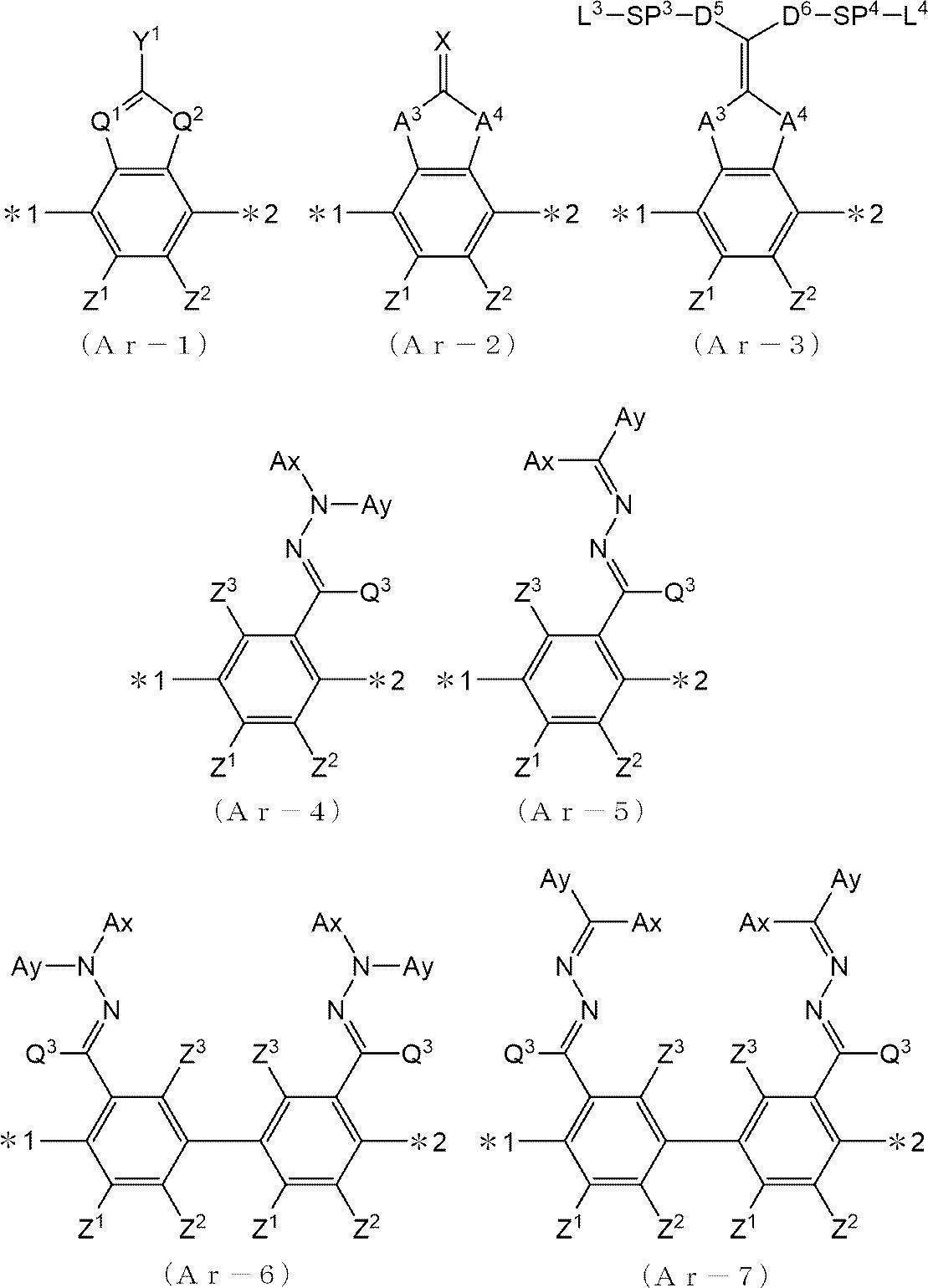
ここで、上記式(Ar-1)中、Q1は、NまたはCHを表し、Q2は、-S-、-O-、または、-N(R5)-を表し、R5は、水素原子または炭素数1~6のアルキル基を表し、Y1は、置換基を有してもよい、炭素数6~12の芳香族炭化水素基、または、炭素数3~12の芳香族複素環基を表す。
R5が示す炭素数1~6のアルキル基としては、例えば、メチル基、エチル基、プロピル基、イソプロピル基、n-ブチル基、イソブチル基、sec-ブチル基、tert-ブチル基、n-ペンチル基、および、n-ヘキシル基などが挙げられる。
Y1が示す炭素数6~12の芳香族炭化水素基としては、例えば、フェニル基、2,6-ジエチルフェニル基、および、ナフチル基などのアリール基が挙げられる。
Y1が示す炭素数3~12の芳香族複素環基としては、例えば、チエニル基、チアゾリル基、フリル基、ピリジル基、および、ベンゾフリル基などのヘテロアリール基が挙げられる。なお、芳香族複素環基には、ベンゼン環と芳香族複素環とが縮合した基も含まれる。
また、Y1が有していてもよい置換基としては、例えば、アルキル基、アルコキシ基、ニトロ基、アルキルスルホニル基、アルキルオキシカルボニル基、シアノ基、および、ハロゲン原子などが挙げられる。
アルキル基としては、例えば、炭素数1~18の直鎖状、分岐鎖状または環状のアルキル基が好ましく、炭素数1~8のアルキル基(例えば、メチル基、エチル基、プロピル基、イソプロピル基、n-ブチル基、イソブチル基、sec-ブチル基、t-ブチル基、および、シクロヘキシル基)がより好ましく、炭素数1~4のアルキル基がさらに好ましく、メチル基またはエチル基が特に好ましい。
アルコキシ基としては、例えば、炭素数1~18のアルコキシ基が好ましく、炭素数1~8のアルコキシ基(例えば、メトキシ基、エトキシ基、n-ブトキシ基、および、メトキシエトキシ基)がより好ましく、炭素数1~4のアルコキシ基がさらに好ましく、メトキシ基またはエトキシ基が特に好ましい。
ハロゲン原子としては、例えば、フッ素原子、塩素原子、臭素原子、および、ヨウ素原子などが挙げられ、フッ素原子、または、塩素原子が好ましい。
R5が示す炭素数1~6のアルキル基としては、例えば、メチル基、エチル基、プロピル基、イソプロピル基、n-ブチル基、イソブチル基、sec-ブチル基、tert-ブチル基、n-ペンチル基、および、n-ヘキシル基などが挙げられる。
Y1が示す炭素数6~12の芳香族炭化水素基としては、例えば、フェニル基、2,6-ジエチルフェニル基、および、ナフチル基などのアリール基が挙げられる。
Y1が示す炭素数3~12の芳香族複素環基としては、例えば、チエニル基、チアゾリル基、フリル基、ピリジル基、および、ベンゾフリル基などのヘテロアリール基が挙げられる。なお、芳香族複素環基には、ベンゼン環と芳香族複素環とが縮合した基も含まれる。
また、Y1が有していてもよい置換基としては、例えば、アルキル基、アルコキシ基、ニトロ基、アルキルスルホニル基、アルキルオキシカルボニル基、シアノ基、および、ハロゲン原子などが挙げられる。
アルキル基としては、例えば、炭素数1~18の直鎖状、分岐鎖状または環状のアルキル基が好ましく、炭素数1~8のアルキル基(例えば、メチル基、エチル基、プロピル基、イソプロピル基、n-ブチル基、イソブチル基、sec-ブチル基、t-ブチル基、および、シクロヘキシル基)がより好ましく、炭素数1~4のアルキル基がさらに好ましく、メチル基またはエチル基が特に好ましい。
アルコキシ基としては、例えば、炭素数1~18のアルコキシ基が好ましく、炭素数1~8のアルコキシ基(例えば、メトキシ基、エトキシ基、n-ブトキシ基、および、メトキシエトキシ基)がより好ましく、炭素数1~4のアルコキシ基がさらに好ましく、メトキシ基またはエトキシ基が特に好ましい。
ハロゲン原子としては、例えば、フッ素原子、塩素原子、臭素原子、および、ヨウ素原子などが挙げられ、フッ素原子、または、塩素原子が好ましい。
また、上記式(Ar-1)~(Ar-7)中、Z1、Z2およびZ3は、それぞれ独立に、水素原子、炭素数1~20の1価の脂肪族炭化水素基、炭素数3~20の1価の脂環式炭化水素基、炭素数6~20の1価の芳香族炭化水素基、ハロゲン原子、シアノ基、ニトロ基、-NR6R7、または、-SR8を表し、R6~R8は、それぞれ独立に、水素原子または炭素数1~6のアルキル基を表し、Z1およびZ2は、互いに結合して環を形成してもよい。環は、脂環式、複素環、および、芳香環のいずれであってもよく、芳香環であることが好ましい。なお、形成される環には、置換基が置換していてもよい。
炭素数1~20の1価の脂肪族炭化水素基としては、炭素数1~15のアルキル基が好ましく、炭素数1~8のアルキル基がより好ましく、メチル基、エチル基、イソプロピル基、tert-ペンチル基(1,1-ジメチルプロピル基)、tert-ブチル基、または、1,1-ジメチル-3,3-ジメチル-ブチル基がさらに好ましく、メチル基、エチル基、または、tert-ブチル基が特に好ましい。
炭素数3~20の1価の脂環式炭化水素基としては、例えば、シクロプロピル基、シクロブチル基、シクロペンチル基、シクロヘキシル基、シクロヘプチル基、シクロオクチル基、シクロデシル基、メチルシクロヘキシル基、および、エチルシクロヘキシル基などの単環式飽和炭化水素基;シクロブテニル基、シクロペンテニル基、シクロヘキセニル基、シクロヘプテニル基、シクロオクテニル基、シクロデセニル基、シクロペンタジエニル基、シクロヘキサジエニル基、シクロオクタジエニル基、および、シクロデカジエン基などの単環式不飽和炭化水素基;ビシクロ[2.2.1]ヘプチル基、ビシクロ[2.2.2]オクチル基、トリシクロ[5.2.1.02,6]デシル基、トリシクロ[3.3.1.13,7]デシル基、テトラシクロ[6.2.1.13,6.02,7]ドデシル基、および、アダマンチル基などの多環式飽和炭化水素基;が挙げられる。
炭素数6~20の1価の芳香族炭化水素基としては、例えば、フェニル基、2,6-ジエチルフェニル基、ナフチル基、および、ビフェニル基などが挙げられ、炭素数6~12のアリール基(特にフェニル基)が好ましい。
ハロゲン原子としては、例えば、フッ素原子、塩素原子、臭素原子、および、ヨウ素原子などが挙げられ、フッ素原子、塩素原子、または、臭素原子が好ましい。
一方、R6~R8が示す炭素数1~6のアルキル基としては、例えば、メチル基、エチル基、プロピル基、イソプロピル基、n-ブチル基、イソブチル基、sec-ブチル基、tert-ブチル基、n-ペンチル基、および、n-ヘキシル基などが挙げられる。
炭素数1~20の1価の脂肪族炭化水素基としては、炭素数1~15のアルキル基が好ましく、炭素数1~8のアルキル基がより好ましく、メチル基、エチル基、イソプロピル基、tert-ペンチル基(1,1-ジメチルプロピル基)、tert-ブチル基、または、1,1-ジメチル-3,3-ジメチル-ブチル基がさらに好ましく、メチル基、エチル基、または、tert-ブチル基が特に好ましい。
炭素数3~20の1価の脂環式炭化水素基としては、例えば、シクロプロピル基、シクロブチル基、シクロペンチル基、シクロヘキシル基、シクロヘプチル基、シクロオクチル基、シクロデシル基、メチルシクロヘキシル基、および、エチルシクロヘキシル基などの単環式飽和炭化水素基;シクロブテニル基、シクロペンテニル基、シクロヘキセニル基、シクロヘプテニル基、シクロオクテニル基、シクロデセニル基、シクロペンタジエニル基、シクロヘキサジエニル基、シクロオクタジエニル基、および、シクロデカジエン基などの単環式不飽和炭化水素基;ビシクロ[2.2.1]ヘプチル基、ビシクロ[2.2.2]オクチル基、トリシクロ[5.2.1.02,6]デシル基、トリシクロ[3.3.1.13,7]デシル基、テトラシクロ[6.2.1.13,6.02,7]ドデシル基、および、アダマンチル基などの多環式飽和炭化水素基;が挙げられる。
炭素数6~20の1価の芳香族炭化水素基としては、例えば、フェニル基、2,6-ジエチルフェニル基、ナフチル基、および、ビフェニル基などが挙げられ、炭素数6~12のアリール基(特にフェニル基)が好ましい。
ハロゲン原子としては、例えば、フッ素原子、塩素原子、臭素原子、および、ヨウ素原子などが挙げられ、フッ素原子、塩素原子、または、臭素原子が好ましい。
一方、R6~R8が示す炭素数1~6のアルキル基としては、例えば、メチル基、エチル基、プロピル基、イソプロピル基、n-ブチル基、イソブチル基、sec-ブチル基、tert-ブチル基、n-ペンチル基、および、n-ヘキシル基などが挙げられる。
また、上記式(Ar-2)および(Ar-3)中、A3およびA4は、それぞれ独立に、-O-、-N(R9)-、-S-、および、-CO-からなる群から選択される基を表し、R9は、水素原子または置換基を表す。
R9が示す置換基としては、上記式(Ar-1)中のY1が有していてもよい置換基と同様のものが挙げられる。
R9が示す置換基としては、上記式(Ar-1)中のY1が有していてもよい置換基と同様のものが挙げられる。
また、上記式(Ar-2)中、Xは、水素原子または置換基が結合していてもよい第14~16族の非金属原子を表す。
また、Xが示す第14族~第16族の非金属原子としては、例えば、酸素原子、硫黄原子、置換基を有する窒素原子、置換基を有する炭素原子が挙げられ、置換基としては、上記式(Ar-1)中のY1が有していてもよい置換基と同様のものが挙げられる。
また、Xが示す第14族~第16族の非金属原子としては、例えば、酸素原子、硫黄原子、置換基を有する窒素原子、置換基を有する炭素原子が挙げられ、置換基としては、上記式(Ar-1)中のY1が有していてもよい置換基と同様のものが挙げられる。
また、上記式(Ar-3)中、D5およびD6は、それぞれ独立に、単結合、-CO-、-O-、-S-、-C(=S)-、-O-CO-、-C(=S)O-、-CR1R2-、-CR1R2-CR3R4-、-O-CR1R2-、-CR1R2-O-CR3R4-、-CO-O-CR1R2-、-O-CO-CR1R2-、-CR1R2-O-CO-CR3R4-、-CR1R2-CO-O-CR3R4-、-NR1-CR2R3-、または、-CO-NR1-を表す。R1、R2、R3およびR4は、それぞれ独立に、水素原子、フッ素原子、または、炭素数1~4のアルキル基を表す。
また、上記式(Ar-3)中、SP3およびSP4は、それぞれ独立に、単結合、炭素数1~12の直鎖状もしくは分岐鎖状のアルキレン基、または、炭素数1~12の直鎖状もしくは分岐鎖状のアルキレン基を構成する-CH2-の1個以上が-O-、-S-、-NH-、-N(Q)-、もしくは、-CO-に置換された2価の連結基を表し、Qは、重合性基を表す。
また、上記式(Ar-3)中、L3およびL4は、それぞれ独立に1価の有機基(例えば、アルキル基、または、重合性基)を表し、上述したように、L3およびL4ならびに上記式(I)中のL1およびL2の少なくとも1つが重合性基を表す。
重合性基以外の1価の有機基としては、例えば、アルキル基、アリール基、及び、ヘテロアリール基が挙げられる。
重合性基以外の1価の有機基としては、例えば、アルキル基、アリール基、及び、ヘテロアリール基が挙げられる。
また、上記式(Ar-4)~(Ar-7)中、Axは、芳香族炭化水素環および芳香族複素環からなる群から選ばれる少なくとも1つの芳香環を有する、炭素数2~30の有機基を表す。
また、上記式(Ar-4)~(Ar-7)中、Ayは、水素原子、置換基を有していてもよい炭素数1~6のアルキル基、または、芳香族炭化水素環および芳香族複素環からなる群から選択される少なくとも1つの芳香環を有する、炭素数2~30の有機基を表す。
ここで、AxおよびAyにおける芳香環は、置換基を有していてもよく、AxとAyとが結合して環を形成していてもよい。
また、Q3は、水素原子、または、置換基を有していてもよい炭素数1~6のアルキル基を表す。
AxおよびAyとしては、国際公開第2014/010325号パンフレットの段落0039~0095に記載されたものが挙げられる。
また、Q3が示す炭素数1~6のアルキル基としては、例えば、メチル基、エチル基、プロピル基、イソプロピル基、n-ブチル基、イソブチル基、sec-ブチル基、tert-ブチル基、n-ペンチル基、および、n-ヘキシル基などが挙げられ、置換基としては、上記式(Ar-1)中のY1が有していてもよい置換基と同様のものが挙げられる。
また、上記式(Ar-4)~(Ar-7)中、Ayは、水素原子、置換基を有していてもよい炭素数1~6のアルキル基、または、芳香族炭化水素環および芳香族複素環からなる群から選択される少なくとも1つの芳香環を有する、炭素数2~30の有機基を表す。
ここで、AxおよびAyにおける芳香環は、置換基を有していてもよく、AxとAyとが結合して環を形成していてもよい。
また、Q3は、水素原子、または、置換基を有していてもよい炭素数1~6のアルキル基を表す。
AxおよびAyとしては、国際公開第2014/010325号パンフレットの段落0039~0095に記載されたものが挙げられる。
また、Q3が示す炭素数1~6のアルキル基としては、例えば、メチル基、エチル基、プロピル基、イソプロピル基、n-ブチル基、イソブチル基、sec-ブチル基、tert-ブチル基、n-ペンチル基、および、n-ヘキシル基などが挙げられ、置換基としては、上記式(Ar-1)中のY1が有していてもよい置換基と同様のものが挙げられる。
なかでも、本発明の効果がより優れる点で、A1およびA2の少なくとも一方が、炭素数6以上のシクロアルキレン環であることが好ましく、A1およびA2の一方が、炭素数6以上のシクロアルキレン環であることがより好ましい。
(色素)
位相差フィルムは、液晶化合物以外の他の成分を合わせて用いて形成してもよい。つまり、位相差フィルムには、上記液晶化合物由来の成分以外の他の成分が含まれていてもよい。
例えば、位相差フィルムには、色素が含まれていてもよい。つまり、位相差フィルムは、液晶化合物および色素を含む組成物を用いて形成された層であってもよい。
色素が含まれることにより、位相差フィルムの波長分散性を制御できる。
以下、まず、一例として、位相差フィルムが赤外線吸収色素を含む場合について詳述する。
まず、図3に、測定波長550nmでの面内レタデーションを1.0として規格化した可視光線領域での各波長における面内レタデーションの波長分散特性を示し、破線で上述した要件2および3に該当する直線を示す。例えば、従来の逆波長分散性を示す位相差フィルムは、図3の実線に示すように、550nm以下の短波長領域においては要件2および3を満たすが、550nm以上の長波長領域においては要件2および3を満たさない傾向を示す場合が多い。
本発明の位相差フィルムにおいては赤外線吸収色素を用いて、かつ、位相差フィルムの波長700~900nmにおける吸収特性を制御することにより、白抜き矢印で示すように、長波長領域における光学特性が要件2および3を満たすように調整できる。
位相差フィルムは、液晶化合物以外の他の成分を合わせて用いて形成してもよい。つまり、位相差フィルムには、上記液晶化合物由来の成分以外の他の成分が含まれていてもよい。
例えば、位相差フィルムには、色素が含まれていてもよい。つまり、位相差フィルムは、液晶化合物および色素を含む組成物を用いて形成された層であってもよい。
色素が含まれることにより、位相差フィルムの波長分散性を制御できる。
以下、まず、一例として、位相差フィルムが赤外線吸収色素を含む場合について詳述する。
まず、図3に、測定波長550nmでの面内レタデーションを1.0として規格化した可視光線領域での各波長における面内レタデーションの波長分散特性を示し、破線で上述した要件2および3に該当する直線を示す。例えば、従来の逆波長分散性を示す位相差フィルムは、図3の実線に示すように、550nm以下の短波長領域においては要件2および3を満たすが、550nm以上の長波長領域においては要件2および3を満たさない傾向を示す場合が多い。
本発明の位相差フィルムにおいては赤外線吸収色素を用いて、かつ、位相差フィルムの波長700~900nmにおける吸収特性を制御することにより、白抜き矢印で示すように、長波長領域における光学特性が要件2および3を満たすように調整できる。
上記特性が得られる理由としては、まず、一般的な有機分子の屈折率波長分散特性について図4を参照しながら説明する。図4中、上側は波長に対する屈折率の挙動を示し、下側では波長に対する吸収特性の挙動(吸収スペクトル)を示す。
有機分子は、固有吸収波長から離れた領域(図4のaの領域)における屈折率nは波長が増すと共に単調に減少する。このような分散は「正常分散」と言われる。これに対して、固有吸収を含む波長域(図4のbの領域)における屈折率nは、波長が増すとともに急激に増加する。このような分散は「異常分散」と言われる。
つまり、図4に示すように、吸収がある波長領域の直前においては屈折率の増減が観察される。
有機分子は、固有吸収波長から離れた領域(図4のaの領域)における屈折率nは波長が増すと共に単調に減少する。このような分散は「正常分散」と言われる。これに対して、固有吸収を含む波長域(図4のbの領域)における屈折率nは、波長が増すとともに急激に増加する。このような分散は「異常分散」と言われる。
つまり、図4に示すように、吸収がある波長領域の直前においては屈折率の増減が観察される。
赤外線吸収色素を用いて、かつ、その配向方向を制御することにより、位相差フィルムにおいては、赤外線吸収色素の影響を受けて、位相差フィルムの進相軸の方向での波長700~900nmにおける吸収が、位相差フィルムの遅相軸の方向での波長700~900nmにおける吸収よりも大きくなる。以後、このような吸収特性を、吸収特性Xともいう。上記吸収特性Xは、位相差フィルム中において赤外線吸収色素の吸光度の高い軸方向を位相差フィルムの進相軸の方向と平行になるように配置することにより達成される。
吸収特性Xを示す位相差フィルムにおいては、吸収特性Xを有さない位相差フィルムよりも、常光線屈折率がより低下する。
具体的には、図5において、上記吸収特性Xの有無による異常光線屈折率neと常光線屈折率noとの波長分散の比較を示す図である。図5中、太線は吸収特性Xがない場合の異常光線屈折率neのカーブを示し、実線は吸収特性Xがない場合の常光線屈折率noのカーブを示す。それに対して、吸収特性Xを有する位相差フィルムにおいては、上記図4で示したような波長700~900nmの吸収に由来する影響を受けて、破線で示すように可視光線領域の長波長領域において常光線屈折率noの値がより低下する。結果として、可視光線領域の長波長領域において、異常光線屈折率neと常光線屈折率noとの差である複屈折Δnがより大きくなり、図3に示す矢印の挙動が達成され、上述した要件2および3(または、要件6)を満たすような位相差フィルムが得られる。
吸収特性Xを示す位相差フィルムにおいては、吸収特性Xを有さない位相差フィルムよりも、常光線屈折率がより低下する。
具体的には、図5において、上記吸収特性Xの有無による異常光線屈折率neと常光線屈折率noとの波長分散の比較を示す図である。図5中、太線は吸収特性Xがない場合の異常光線屈折率neのカーブを示し、実線は吸収特性Xがない場合の常光線屈折率noのカーブを示す。それに対して、吸収特性Xを有する位相差フィルムにおいては、上記図4で示したような波長700~900nmの吸収に由来する影響を受けて、破線で示すように可視光線領域の長波長領域において常光線屈折率noの値がより低下する。結果として、可視光線領域の長波長領域において、異常光線屈折率neと常光線屈折率noとの差である複屈折Δnがより大きくなり、図3に示す矢印の挙動が達成され、上述した要件2および3(または、要件6)を満たすような位相差フィルムが得られる。
なお、上記では赤外線吸収色素を用いる形態について説明したが、この形態には限定されず、可視光領域に極大吸収波長を有する二色性色素(以後、「可視光吸収二色性色素」ともいう)を用いる形態が挙げられる。
可視光吸収二色性色素が位相差フィルム中にあると、上述した赤外線吸収色素を用いる場合と同様に、位相差フィルムの波長分散性に影響を与える。例えば、550nm付近に極大吸収波長を有する二色性色素を液晶化合物と共に用いて位相差フィルムを作製した場合、図4で示した屈折率波長分散特性の影響を受けて、図6に示すように、550nm付近に極大吸収波長を有する二色性色素を用いずに作製した位相差フィルムの波長分散特性(図6中の実線で示す)に対して、550nm以下の短波長領域においては黒矢印の方向に、550nm以上の長波長領域においては白矢印方向に曲線が移動して、上述した要件2および3(または、要件6)を満たすような位相差フィルムが得られる。
可視光吸収二色性色素が位相差フィルム中にあると、上述した赤外線吸収色素を用いる場合と同様に、位相差フィルムの波長分散性に影響を与える。例えば、550nm付近に極大吸収波長を有する二色性色素を液晶化合物と共に用いて位相差フィルムを作製した場合、図4で示した屈折率波長分散特性の影響を受けて、図6に示すように、550nm付近に極大吸収波長を有する二色性色素を用いずに作製した位相差フィルムの波長分散特性(図6中の実線で示す)に対して、550nm以下の短波長領域においては黒矢印の方向に、550nm以上の長波長領域においては白矢印方向に曲線が移動して、上述した要件2および3(または、要件6)を満たすような位相差フィルムが得られる。
以下、色素の形態について、赤外線吸収色素と可視光吸収二色性色素との形態に分けて説明する。
赤外線吸収色素としては、赤外線(特に、波長700~900mの光)を吸収する色素であれば特に制限されない。なかでも、赤外線吸収色素は二色性色素であることが好ましい。なお、二色性色素とは、分子の長軸方向における吸光度と、短軸方向における吸光度とが異なる性質を有する色素をいう。
赤外線吸収色素としては、ジケトピロロピロール系色素、ジインモニウム系色素、フタロシアニン系色素、ナフタロシアニン系色素、アゾ系色素、ポリメチン系色素、アントラキノン系色素、ピリリウム系色素、スクアリリウム系色素、トリフェニルメタン系色素、シアニン系色素、および、アミニウム系色素などが挙げられる。
赤外線吸収色素は1種単独で用いてもよいし、2種類以上を組み合わせて用いてもよい。
赤外線吸収色素としては、ジケトピロロピロール系色素、ジインモニウム系色素、フタロシアニン系色素、ナフタロシアニン系色素、アゾ系色素、ポリメチン系色素、アントラキノン系色素、ピリリウム系色素、スクアリリウム系色素、トリフェニルメタン系色素、シアニン系色素、および、アミニウム系色素などが挙げられる。
赤外線吸収色素は1種単独で用いてもよいし、2種類以上を組み合わせて用いてもよい。
本発明の効果がより優れる点で、赤外線吸収色素はメソゲン基を有することが好ましい。赤外線吸収色素がメソゲン基を有することにより、上述した液晶化合物と共に配向しやすく、所定の吸収特性の制御がしやすい。
メソゲン基とは、剛直かつ配向性を有する官能基である。メソゲン基の構造としては、例えば、芳香環基(芳香族炭化水素環基および芳香族複素環基)および脂環基からなる群から選択される基が、複数個、直接または連結基(例えば、-CO-、-O-、-NR-(Rは、水素原子、または、アルキル基を表す)、または、これらを組み合わせた基)を介して連なった構造が挙げられる。
メソゲン基とは、剛直かつ配向性を有する官能基である。メソゲン基の構造としては、例えば、芳香環基(芳香族炭化水素環基および芳香族複素環基)および脂環基からなる群から選択される基が、複数個、直接または連結基(例えば、-CO-、-O-、-NR-(Rは、水素原子、または、アルキル基を表す)、または、これらを組み合わせた基)を介して連なった構造が挙げられる。
赤外線吸収色素の極大吸収波長は、本発明の効果がより優れる点で、700~900nmに位置することが好ましい。
赤外線吸収色素の好適形態としては、式(1)で表される化合物が挙げられる。
式(1)で表される化合物は、可視光線領域の吸収が少なく、得られる位相差フィルムの着色がより抑制される。また、この化合物はメソゲン基を有する基を含むことから、液晶化合物と共に配向しやすい。その際、化合物の中心にある窒素原子を含む縮合環部分から横方向に延びる形でメソゲン基を有する基が配置されているため、形成される位相差フィルムの遅相軸に対して、上記縮合環部分が直交する方向に配列しやすい。つまり、位相差フィルムの遅相軸に直交する方向に、縮合環部分に由来する赤外線領域(特に、波長700~900nm)における吸収が得られやすく、所望の特性を示す位相差フィルムが得られやすい。
式(1)で表される化合物は、可視光線領域の吸収が少なく、得られる位相差フィルムの着色がより抑制される。また、この化合物はメソゲン基を有する基を含むことから、液晶化合物と共に配向しやすい。その際、化合物の中心にある窒素原子を含む縮合環部分から横方向に延びる形でメソゲン基を有する基が配置されているため、形成される位相差フィルムの遅相軸に対して、上記縮合環部分が直交する方向に配列しやすい。つまり、位相差フィルムの遅相軸に直交する方向に、縮合環部分に由来する赤外線領域(特に、波長700~900nm)における吸収が得られやすく、所望の特性を示す位相差フィルムが得られやすい。

R11およびR12は、それぞれ独立に、水素原子または置換基を表し、少なくとも一方は電子吸引性基であり、R11およびR12は結合して環を形成してもよい。
置換基としては、例えば、アルキル基、アルケニル基、アルキニル基、アリール基、アミノ基、アルコキシ基、アリールオキシ基、芳香族ヘテロ環オキシ基、アシル基、アルコキシカルボニル基、アリールオキシカルボニル基、アシルオキシ基、アシルアミノ基、アルコキシカルボニルアミノ基、アリールオキシカルボニルアミノ基、スルホニルアミノ基、スルファモイル基、カルバモイル基、アルキルチオ基、アリールチオ基、芳香族ヘテロ環チオ基、スルホニル基、スルフィニル基、ウレイド基、リン酸アミド基、ヒドロキシ基、メルカプト基、ハロゲン原子、シアノ基、スルホ基、カルボキシル基、ニトロ基、ヒドロキサム酸基、スルフィノ基、ヒドラジノ基、イミノ基、ヘテロ環基(例えば、ヘテロアリール基)、シリル基、および、これらを組み合わせた基などが挙げられる。なお、上記置換基は、さらに置換基で置換されていてもよい。
なお、R11およびR12で表される置換基としては、後述するメソゲン基を有する基以外の基が好ましい。
置換基としては、例えば、アルキル基、アルケニル基、アルキニル基、アリール基、アミノ基、アルコキシ基、アリールオキシ基、芳香族ヘテロ環オキシ基、アシル基、アルコキシカルボニル基、アリールオキシカルボニル基、アシルオキシ基、アシルアミノ基、アルコキシカルボニルアミノ基、アリールオキシカルボニルアミノ基、スルホニルアミノ基、スルファモイル基、カルバモイル基、アルキルチオ基、アリールチオ基、芳香族ヘテロ環チオ基、スルホニル基、スルフィニル基、ウレイド基、リン酸アミド基、ヒドロキシ基、メルカプト基、ハロゲン原子、シアノ基、スルホ基、カルボキシル基、ニトロ基、ヒドロキサム酸基、スルフィノ基、ヒドラジノ基、イミノ基、ヘテロ環基(例えば、ヘテロアリール基)、シリル基、および、これらを組み合わせた基などが挙げられる。なお、上記置換基は、さらに置換基で置換されていてもよい。
なお、R11およびR12で表される置換基としては、後述するメソゲン基を有する基以外の基が好ましい。
電子吸引性基としては、Hammettのσp値(シグマパラ値)が正の置換基を表し、例えば、シアノ基、アシル基、アルキルオキシカルボニル基、アリールオキシカルボニル基、スルファモイル基、スルフィニル基、および、ヘテロ環基が挙げられる。
これら電子吸引性基はさらに置換されていてもよい。
ハメットの置換基定数σ値について説明する。ハメット則は、ベンゼン誘導体の反応または平衡に及ぼす置換基の影響を定量的に論ずるために1935年L.P.Hammettにより提唱された経験則であるが、これは今日広く妥当性が認められている。ハメット則に求められた置換基定数にはσp値とσm値があり、これらの値は多くの一般的な成書に見出すことができる。例えば、J.A.Dean編、「Lange’s Handbook of Chemistry」第12版,1979年(Mc Graw-Hill)や「化学の領域」増刊,122号,96~103頁,1979年(南光堂)、Chem.Rev.,1991年,91巻,165~195ページなどに詳しい。本発明において電子吸引性基としては、ハメットの置換基定数σp値が0.20以上の置換基が好ましい。σp値としては、0.25以上が好ましく、0.30以上がより好ましく、0.35以上がさらに好ましい。上限は特に制限はないが、0.80以下が好ましい。
具体例としては、シアノ基(0.66)、カルボキシル基(-COOH:0.45)、アルコキシカルボニル基(-COOMe:0.45)、アリールオキシカルボニル基(-COOPh:0.44)、カルバモイル基(-CONH2:0.36)、アルキルカルボニル基(-COMe:0.50)、アリールカルボニル基(-COPh:0.43)、アルキルスルホニル基(-SO2Me:0.72)、および、アリールスルホニル基(-SO2Ph:0.68)が挙げられる。
本明細書において、Meはメチル基を、Phはフェニル基を表す。なお、括弧内の値は代表的な置換基のσp値をChem.Rev.,1991年,91巻,165~195ページから抜粋したものである。
これら電子吸引性基はさらに置換されていてもよい。
ハメットの置換基定数σ値について説明する。ハメット則は、ベンゼン誘導体の反応または平衡に及ぼす置換基の影響を定量的に論ずるために1935年L.P.Hammettにより提唱された経験則であるが、これは今日広く妥当性が認められている。ハメット則に求められた置換基定数にはσp値とσm値があり、これらの値は多くの一般的な成書に見出すことができる。例えば、J.A.Dean編、「Lange’s Handbook of Chemistry」第12版,1979年(Mc Graw-Hill)や「化学の領域」増刊,122号,96~103頁,1979年(南光堂)、Chem.Rev.,1991年,91巻,165~195ページなどに詳しい。本発明において電子吸引性基としては、ハメットの置換基定数σp値が0.20以上の置換基が好ましい。σp値としては、0.25以上が好ましく、0.30以上がより好ましく、0.35以上がさらに好ましい。上限は特に制限はないが、0.80以下が好ましい。
具体例としては、シアノ基(0.66)、カルボキシル基(-COOH:0.45)、アルコキシカルボニル基(-COOMe:0.45)、アリールオキシカルボニル基(-COOPh:0.44)、カルバモイル基(-CONH2:0.36)、アルキルカルボニル基(-COMe:0.50)、アリールカルボニル基(-COPh:0.43)、アルキルスルホニル基(-SO2Me:0.72)、および、アリールスルホニル基(-SO2Ph:0.68)が挙げられる。
本明細書において、Meはメチル基を、Phはフェニル基を表す。なお、括弧内の値は代表的な置換基のσp値をChem.Rev.,1991年,91巻,165~195ページから抜粋したものである。
R11およびR12が結合して環を形成する場合は、5~7員環(好ましくは5~6員環)の環を形成し、形成される環としては通常メロシアニン色素で酸性核として用いられるものが好ましい。
R11およびR12が結合して形成される環としては、1,3-ジカルボニル核、ピラゾリノン核、2,4,6-トリケトヘキサヒドロピリミジン核(チオケトン体も含む)、2-チオ-2,4-チアゾリジンジオン核、2-チオ-2,4-オキサゾリジンジオン核、2-チオ-2,5-チアゾリジンジオン核、2,4-チアゾリジンジオン核、2,4-イミダゾリジンジオン核、2-チオ-2,4-イミダゾリジンジオン核、2-イミダゾリン-5-オン核、3,5-ピラゾリジンジオン核、ベンゾチオフェン-3-オン核、またはインダノン核が好ましい。
R11およびR12が結合して形成される環としては、1,3-ジカルボニル核、ピラゾリノン核、2,4,6-トリケトヘキサヒドロピリミジン核(チオケトン体も含む)、2-チオ-2,4-チアゾリジンジオン核、2-チオ-2,4-オキサゾリジンジオン核、2-チオ-2,5-チアゾリジンジオン核、2,4-チアゾリジンジオン核、2,4-イミダゾリジンジオン核、2-チオ-2,4-イミダゾリジンジオン核、2-イミダゾリン-5-オン核、3,5-ピラゾリジンジオン核、ベンゾチオフェン-3-オン核、またはインダノン核が好ましい。
R11は、ヘテロ環基であることが好ましく、芳香族ヘテロ環基であることがより好ましい。ヘテロ環基は、単環であっても、多環であってもよい。ヘテロ環基としては、ピラゾール環基、チアゾール環基、オキサゾール環基、イミダゾール環基、オキサジアゾール環基、チアジアゾール環基、トリアゾール環基、ピリジン環基、ピリダジン環基、ピリミジン環基、ピラジン環基、これらのベンゾ縮環基(例えば、ベンゾチアゾール環基、ベンゾピラジン環基)もしくはナフト縮環基、または、これら縮環の複合体が好ましい。
上記ヘテロ環基には、置換基が置換していてもよい。置換基としては、上述したR11およびR12で表される置換基で例示した置換基の例が挙げられる。
上記ヘテロ環基には、置換基が置換していてもよい。置換基としては、上述したR11およびR12で表される置換基で例示した置換基の例が挙げられる。
R13は、それぞれ独立に、水素原子、アルキル基、アリール基、ヘテロアリール基、置換ホウ素(-B(Ra)2、Raは置換基を表す)または金属原子を表し、R11と共有結合または配位結合していてもよい。
R13で表される置換ホウ素の置換基は、R11およびR12について上述した置換基と同義であり、アルキル基、アリール基、または、ヘテロアリール基が好ましい。置換ホウ素の置換基(例えば、上述した、アルキル基、アリール基、または、ヘテロアリール基)は、さらに置換基で置換されていてもよい。置換基としては、R11およびR12で表される置換基で例示した基が挙げられる。
また、R13で表される金属原子は、遷移金属原子、マグネシウム原子、アルミニウム原子、カルシウム原子、バリウム原子、亜鉛原子、または、スズ原子が好ましく、アルミニウム原子、亜鉛原子、スズ原子、バナジウム原子、鉄原子、コバルト原子、ニッケル原子、銅原子、パラジウム原子、イリジウム原子、または、白金原子がより好ましい。
R13で表される置換ホウ素の置換基は、R11およびR12について上述した置換基と同義であり、アルキル基、アリール基、または、ヘテロアリール基が好ましい。置換ホウ素の置換基(例えば、上述した、アルキル基、アリール基、または、ヘテロアリール基)は、さらに置換基で置換されていてもよい。置換基としては、R11およびR12で表される置換基で例示した基が挙げられる。
また、R13で表される金属原子は、遷移金属原子、マグネシウム原子、アルミニウム原子、カルシウム原子、バリウム原子、亜鉛原子、または、スズ原子が好ましく、アルミニウム原子、亜鉛原子、スズ原子、バナジウム原子、鉄原子、コバルト原子、ニッケル原子、銅原子、パラジウム原子、イリジウム原子、または、白金原子がより好ましい。
R14は、それぞれ独立に、メソゲン基を有する基を表す。メソゲン基の定義は、上述した通りである。
R14は、式(2)で表される基であることが好ましい。*は、結合位置を表す。
式(2) *-M1-(X1-M2)n-X2-P
M1は、置換もしくは無置換のアリーレン基、または、置換もしくは無置換のヘテロアリーレン基を表す。アリーレン基としては、フェニレン基が挙げられる。ヘテロアリーレン基としては、ピラゾール環、チアゾール環、オキサゾール環、イミダゾール環、オキサジアゾール環、チアジアゾール環、トリアゾール環、ピリジン環、ピリダジン環、ピリミジン環、ピラジン環、これらのベンゾ縮環(例えば、ベンゾチアゾール環、ベンゾピラジン環)もしくはナフト縮環、または、これら縮環の複合体から任意の2つの水素原子を除いた2価の基が挙げられる。上記アリーレン基および上記ヘテロアリーレン基が置換基を有する場合、置換基としては、R11およびR12で表される置換基で例示した基が挙げられる。
X1は、単結合、-O-、-CO-、-C(R0)2-、-CH=CH-、-CH=N-、-N=N-、-C≡C-、-NR0-、または、これらの組み合わせ(例えば、-COO-、-CONR0-、-COOCH2CH2-、-CONRCH2CH2-、-OCOCH=CH-、および、-C≡C-C≡C-)を表す。R0は、水素原子または炭素数1~5のアルキル基を表す。
M2は、置換もしくは無置換のアリーレン基、置換もしくは無置換のヘテロアリーレン基、または、置換もしくは無置換のシクロアルキレン基を表す。アリーレン基としては、フェニレン基が挙げられる。ヘテロアリーレン基としては、ピラゾール環、チアゾール環、オキサゾール環、イミダゾール環、オキサジアゾール環、チアジアゾール環、トリアゾール環、ピリジン環、ピリダジン環、ピリミジン環、ピラジン環、これらのベンゾ縮環(例えば、ベンゾチアゾール環、ベンゾピラジン環)もしくはナフト縮環、または、これら縮環の複合体から任意の2つの水素原子を除いた2価の基が挙げられる。シクロアルキレン基に含まれる炭素数は、5~7が好ましい。上記アリーレン基、上記ヘテロアリーレン基、および、上記シクロアルキレン基が置換基を有する場合、置換基としては、R11およびR12で表される置換基で例示した基が挙げられる。
X2は、単結合または2価の連結基を表す。2価の連結基としては、例えば、2価の炭化水素基(例えば、炭素数1~10のアルキレン基、炭素数1~10のアルケニレン基、および、炭素数1~10のアルキニレン基などの2価の脂肪族炭化水素基、アリーレン基などの2価の芳香族炭化水素基)、2価の複素環基、-O-、-S-、-NH-、-N(Q)-、-CO-、または、これらを組み合わせた基(例えば、-O-2価の炭化水素基-、-(O-2価の炭化水素基)m-O-(mは、1以上の整数を表す)、および、-2価の炭化水素基-O-CO-など)が挙げられる。Qは、水素原子またはアルキル基を表す。
nは1~10を表す。なかでも、1~5が好ましく、2~4がより好ましい。
Pは、水素原子、または、重合性基を表す。重合性基の定義は、後述する液晶化合物が有していてもよい重合性基の定義と同義である。
R14は、式(2)で表される基であることが好ましい。*は、結合位置を表す。
式(2) *-M1-(X1-M2)n-X2-P
M1は、置換もしくは無置換のアリーレン基、または、置換もしくは無置換のヘテロアリーレン基を表す。アリーレン基としては、フェニレン基が挙げられる。ヘテロアリーレン基としては、ピラゾール環、チアゾール環、オキサゾール環、イミダゾール環、オキサジアゾール環、チアジアゾール環、トリアゾール環、ピリジン環、ピリダジン環、ピリミジン環、ピラジン環、これらのベンゾ縮環(例えば、ベンゾチアゾール環、ベンゾピラジン環)もしくはナフト縮環、または、これら縮環の複合体から任意の2つの水素原子を除いた2価の基が挙げられる。上記アリーレン基および上記ヘテロアリーレン基が置換基を有する場合、置換基としては、R11およびR12で表される置換基で例示した基が挙げられる。
X1は、単結合、-O-、-CO-、-C(R0)2-、-CH=CH-、-CH=N-、-N=N-、-C≡C-、-NR0-、または、これらの組み合わせ(例えば、-COO-、-CONR0-、-COOCH2CH2-、-CONRCH2CH2-、-OCOCH=CH-、および、-C≡C-C≡C-)を表す。R0は、水素原子または炭素数1~5のアルキル基を表す。
M2は、置換もしくは無置換のアリーレン基、置換もしくは無置換のヘテロアリーレン基、または、置換もしくは無置換のシクロアルキレン基を表す。アリーレン基としては、フェニレン基が挙げられる。ヘテロアリーレン基としては、ピラゾール環、チアゾール環、オキサゾール環、イミダゾール環、オキサジアゾール環、チアジアゾール環、トリアゾール環、ピリジン環、ピリダジン環、ピリミジン環、ピラジン環、これらのベンゾ縮環(例えば、ベンゾチアゾール環、ベンゾピラジン環)もしくはナフト縮環、または、これら縮環の複合体から任意の2つの水素原子を除いた2価の基が挙げられる。シクロアルキレン基に含まれる炭素数は、5~7が好ましい。上記アリーレン基、上記ヘテロアリーレン基、および、上記シクロアルキレン基が置換基を有する場合、置換基としては、R11およびR12で表される置換基で例示した基が挙げられる。
X2は、単結合または2価の連結基を表す。2価の連結基としては、例えば、2価の炭化水素基(例えば、炭素数1~10のアルキレン基、炭素数1~10のアルケニレン基、および、炭素数1~10のアルキニレン基などの2価の脂肪族炭化水素基、アリーレン基などの2価の芳香族炭化水素基)、2価の複素環基、-O-、-S-、-NH-、-N(Q)-、-CO-、または、これらを組み合わせた基(例えば、-O-2価の炭化水素基-、-(O-2価の炭化水素基)m-O-(mは、1以上の整数を表す)、および、-2価の炭化水素基-O-CO-など)が挙げられる。Qは、水素原子またはアルキル基を表す。
nは1~10を表す。なかでも、1~5が好ましく、2~4がより好ましい。
Pは、水素原子、または、重合性基を表す。重合性基の定義は、後述する液晶化合物が有していてもよい重合性基の定義と同義である。
赤外線吸収色素は、式(3)で表される化合物であることがより好ましい。
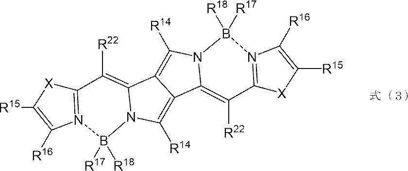
R14の定義は、上述した通りである。
R22は、それぞれ独立に、シアノ基、アシル基、アルコキシカルボニル基、アルキルスルフィニル基、アリールスルフィニル基、または、含窒素ヘテロアリール基を表す。
R15およびR16は、それぞれ独立に、水素原子、アルキル基、アルコキシ基、アリール基、または、ヘテロアリール基を表し、R15およびR16は結合して環を形成してよい。形成される環としては、炭素数5~10の脂環、炭素数6~10の芳香族炭化水素環、または、炭素数3~10の芳香族複素環が挙げられる。R15およびR16が結合して形成される環には、さらに置換基が置換していてもよい。置換基としては、R11およびR12で表される置換基の説明で例示した基が挙げられる。
R17およびR18は、それぞれ独立に、アルキル基、アルコキシ基、アリール基、または、ヘテロアリール基を表す。R17およびR18で表される基には、さらに置換基が置換してもよい。置換基としては、R11およびR12で表される置換基の説明で例示した基が挙げられる。
Xは、それぞれ独立に、酸素原子、硫黄原子、-NR-、-CRR’-、-CH=CH-、または、-N=CH-を表し、RおよびR’は、それぞれ独立に、水素原子、アルキル基、または、アリール基を表す。
R22は、それぞれ独立に、シアノ基、アシル基、アルコキシカルボニル基、アルキルスルフィニル基、アリールスルフィニル基、または、含窒素ヘテロアリール基を表す。
R15およびR16は、それぞれ独立に、水素原子、アルキル基、アルコキシ基、アリール基、または、ヘテロアリール基を表し、R15およびR16は結合して環を形成してよい。形成される環としては、炭素数5~10の脂環、炭素数6~10の芳香族炭化水素環、または、炭素数3~10の芳香族複素環が挙げられる。R15およびR16が結合して形成される環には、さらに置換基が置換していてもよい。置換基としては、R11およびR12で表される置換基の説明で例示した基が挙げられる。
R17およびR18は、それぞれ独立に、アルキル基、アルコキシ基、アリール基、または、ヘテロアリール基を表す。R17およびR18で表される基には、さらに置換基が置換してもよい。置換基としては、R11およびR12で表される置換基の説明で例示した基が挙げられる。
Xは、それぞれ独立に、酸素原子、硫黄原子、-NR-、-CRR’-、-CH=CH-、または、-N=CH-を表し、RおよびR’は、それぞれ独立に、水素原子、アルキル基、または、アリール基を表す。
可視光吸収二色性色素としては特に制限されないが、例えば、アクリジン色素、アジン色素、アゾメチン色素、オキサジン色素、シアニン色素、メロシアニン色素、スクアリリウム色素、ナフタレン色素、アゾ色素、及びアントラキノン色素、ベンゾトリアゾール色素、ベンゾフェノン色素、ピラゾリン色素、ジフェニルポリエン色素、ビナフチルポリエン色素、スチルベン色素、ベンゾチアゾール色素、チエノチアゾール色素、ベンゾイミダゾール色素、クマリン色素、ニトロジフェニルアミン色素、ポリメチン色素、ナフトキノン色素、ペリレン色素、キノフタロン色素、スチルベン色素、および、インジゴ色素が挙げられる。
可視光吸収二色性色素の二色比は、可視光吸収二色性色素の長軸方向における極大吸収波長での吸光度と短軸方向の吸光度の比で定義される。二色比は、可視光吸収二色性色素の配向方向の吸光度および配向方向と垂直方向の吸光度を測定することで求めることが可能である。可視光吸収二色性色素の二色比は、2~50が好ましく、5~30がより好ましい。
なお、可視光吸収二色性色素は、重合性基を有していてもよい。重合性基としては、アクリル基、メタクリル基、ビニル基、ビニロキシ基、エポキシ基、および、オキセタニル基が挙げられる。
可視光吸収二色性色素の極大吸収波長は、400~700nmの範囲内に位置することが好ましく、540~620nmの範囲に位置することがより好ましい。
(製造方法)
位相差フィルムの製造方法は特に制限されず、公知の方法が挙げられる。
なかでも、位相差フィルムの波長分散特性の制御がしやすい点から、重合性基を有する液晶化合物(以後、単に「重合性液晶化合物」とも称する)および上記色素(例えば、赤外線吸収色素または可視光吸収二色性色素)を含む位相差フィルム形成用組成物(以後、単に「組成物」とも称する)を塗布して塗膜を形成し、塗膜に配向処理を施して重合性液晶化合物を配向させ、得られた塗膜に対して硬化処理(紫外線の照射(光照射処理)または加熱処理)を施して、位相差フィルムを形成する方法が好ましい。
以下、上記方法の手順について詳述する。
位相差フィルムの製造方法は特に制限されず、公知の方法が挙げられる。
なかでも、位相差フィルムの波長分散特性の制御がしやすい点から、重合性基を有する液晶化合物(以後、単に「重合性液晶化合物」とも称する)および上記色素(例えば、赤外線吸収色素または可視光吸収二色性色素)を含む位相差フィルム形成用組成物(以後、単に「組成物」とも称する)を塗布して塗膜を形成し、塗膜に配向処理を施して重合性液晶化合物を配向させ、得られた塗膜に対して硬化処理(紫外線の照射(光照射処理)または加熱処理)を施して、位相差フィルムを形成する方法が好ましい。
以下、上記方法の手順について詳述する。
まず、支持体上に、組成物を塗布して塗膜を形成し、塗膜に配向処理を施して重合性液晶化合物を配向させる。重合性液晶化合物の配向にあわせて、色素も所定の方向に配向する。
使用される組成物は、重合性液晶化合物を含む。重合性液晶化合物の定義は、上述した通りである。
また、使用される組成物は、赤外線吸収色素または可視光吸収二色性色素などの色素を含む。
使用される組成物は、重合性液晶化合物を含む。重合性液晶化合物の定義は、上述した通りである。
また、使用される組成物は、赤外線吸収色素または可視光吸収二色性色素などの色素を含む。
組成物中における重合性液晶化合物の含有量は特に制限されないが、組成物中の全固形分に対して、50質量%以上が好ましく、70質量%以上がより好ましく、90質量%以上がさらに好ましい。上限は特に制限されないが、99質量%以下の場合が多い。
なお、組成物中の全固形分には、溶媒は含まれない。
なお、組成物中の全固形分には、溶媒は含まれない。
組成物中における色素の含有量は特に制限されないが、組成物中に赤外線吸収色素が含まれる場合、赤外線吸収色素の含有量は、重合性液晶化合物100質量部に対して、1~20質量部が好ましく、3~15質量部がより好ましい。
組成物中に可視光吸収二色性色素が含まれる場合、可視光吸収二色性色素の含有量は、重合性液晶化合物100質量部に対して、0.01~0.50質量部が好ましく、0.01~0.20質量部がより好ましく、0.05~0.15質量部がさらに好ましい。
組成物中に可視光吸収二色性色素が含まれる場合、可視光吸収二色性色素の含有量は、重合性液晶化合物100質量部に対して、0.01~0.50質量部が好ましく、0.01~0.20質量部がより好ましく、0.05~0.15質量部がさらに好ましい。
組成物には、重合性基を有さない液晶化合物が含まれていてもよい。重合性基を有さない液晶化合物としては、例えば、式(I)中のL1およびL2がいずれも重合性基以外の基である液晶化合物が挙げられる。
また、組成物には、重合開始剤が含まれていてもよい。使用される重合開始剤は、重合反応の形式に応じて選択され、例えば、熱重合開始剤、および、光重合開始剤が挙げられる。例えば、光重合開始剤としては、α-カルボニル化合物、アシロインエーテル、α-炭化水素置換芳香族アシロイン化合物、多核キノン化合物、および、トリアリールイミダゾールダイマーとp-アミノフェニルケトンとの組み合わせなどが挙げられる。
組成物中における重合開始剤の含有量は、組成物の全固形分に対して、0.01~20質量%が好ましく、0.5~5質量%がより好ましい。
組成物中における重合開始剤の含有量は、組成物の全固形分に対して、0.01~20質量%が好ましく、0.5~5質量%がより好ましい。
また、組成物には、重合性液晶化合物以外の重合性モノマーが含まれていてもよい。
重合性モノマーとしては、ラジカル重合性またはカチオン重合性の化合物が挙げられる。なかでも、多官能性ラジカル重合性モノマーが好ましい。また、重合性モノマーとしては、上記の重合性基を有する液晶化合物と共重合性のモノマーが好ましい。例えば、特開2002-296423号公報中の段落[0018]~[0020]に記載の重合性モノマーが挙げられる。
組成物中における重合性モノマーの含有量は、重合性液晶化合物の全質量に対して、1~50質量%が好ましく、2~30質量%がより好ましい。
重合性モノマーとしては、ラジカル重合性またはカチオン重合性の化合物が挙げられる。なかでも、多官能性ラジカル重合性モノマーが好ましい。また、重合性モノマーとしては、上記の重合性基を有する液晶化合物と共重合性のモノマーが好ましい。例えば、特開2002-296423号公報中の段落[0018]~[0020]に記載の重合性モノマーが挙げられる。
組成物中における重合性モノマーの含有量は、重合性液晶化合物の全質量に対して、1~50質量%が好ましく、2~30質量%がより好ましい。
また、組成物には、界面活性剤が含まれていてもよい。
界面活性剤としては、従来公知の化合物が挙げられるが、特にフッ素系化合物が好ましい。例えば、特開2001-330725号公報中の段落[0028]~[0056]に記載の化合物、および、特願2003-295212号明細書中の段落[0069]~[0126]に記載の化合物が挙げられる。
界面活性剤としては、従来公知の化合物が挙げられるが、特にフッ素系化合物が好ましい。例えば、特開2001-330725号公報中の段落[0028]~[0056]に記載の化合物、および、特願2003-295212号明細書中の段落[0069]~[0126]に記載の化合物が挙げられる。
また、組成物には、溶媒が含まれていてもよい。溶媒としては、有機溶媒が好ましい。有機溶媒としては、アミド(例:N,N-ジメチルホルムアミド)、スルホキシド(例:ジメチルスルホキシド)、ヘテロ環化合物(例:ピリジン)、炭化水素(例:ベンゼン、ヘキサン)、アルキルハライド(例:クロロホルム、ジクロロメタン)、エステル(例:酢酸メチル、酢酸エチル、酢酸ブチル)、ケトン(例:アセトン、メチルエチルケトン)、および、エーテル(例:テトラヒドロフラン、1,2-ジメトキシエタン)が挙げられる。なお、2種類以上の有機溶媒を併用してもよい。
また、組成物には、垂直配向剤、および、水平配向剤などの各種配向制御剤が含まれていてもよい。これらの配向制御剤は、界面側において液晶化合物を水平または垂直に配向制御可能な化合物である。
さらに、組成物には、上記成分以外に、密着改良剤、可塑剤、および、ポリマーなどが含まれていてもよい。
さらに、組成物には、上記成分以外に、密着改良剤、可塑剤、および、ポリマーなどが含まれていてもよい。
使用される支持体は、組成物を塗布するための基材として機能を有する部材である。支持体は、組成物を塗布および硬化させた後に剥離される仮支持体であってもよい。
支持体(仮支持体)としては、プラスチックフィルムの他、ガラス基板を用いてもよい。プラスチックフィルムを構成する材料としては、ポリエチレンテレフタレート(PET)などのポリエステル樹脂、ポリカーボネート樹脂、(メタ)アクリル樹脂、エポキシ樹脂、ポリウレタン樹脂、ポリアミド樹脂、ポリオレフィン樹脂、セルロース誘導体、シリコーン樹脂、および、ポリビニルアルコール(PVA)などが挙げられる。
支持体の厚みは、5~1000μm程度であればよく、10~250μmが好ましく、15~90μmがより好ましい。
支持体(仮支持体)としては、プラスチックフィルムの他、ガラス基板を用いてもよい。プラスチックフィルムを構成する材料としては、ポリエチレンテレフタレート(PET)などのポリエステル樹脂、ポリカーボネート樹脂、(メタ)アクリル樹脂、エポキシ樹脂、ポリウレタン樹脂、ポリアミド樹脂、ポリオレフィン樹脂、セルロース誘導体、シリコーン樹脂、および、ポリビニルアルコール(PVA)などが挙げられる。
支持体の厚みは、5~1000μm程度であればよく、10~250μmが好ましく、15~90μmがより好ましい。
なお、必要に応じて、支持体上には、配向膜を配置してもよい。
配向膜は、一般的には、ポリマーを主成分とする。配向膜用ポリマーとしては、多数の文献に記載があり、多数の市販品を入手できる。利用されるポリマーは、ポリビニルアルコール、ポリイミド、または、その誘導体が好ましい。
なお、配向膜には、公知のラビング処理が施されることが好ましい。
配向膜の厚みは、0.01~10μmが好ましく、0.01~1μmがより好ましい。
配向膜は、一般的には、ポリマーを主成分とする。配向膜用ポリマーとしては、多数の文献に記載があり、多数の市販品を入手できる。利用されるポリマーは、ポリビニルアルコール、ポリイミド、または、その誘導体が好ましい。
なお、配向膜には、公知のラビング処理が施されることが好ましい。
配向膜の厚みは、0.01~10μmが好ましく、0.01~1μmがより好ましい。
組成物の塗布方法としては、カーテンコーティング法、ディップコーティング法、スピンコーティング法、印刷コーティング法、スプレーコーティング法、スロットコーティング法、ロールコーティング法、スライドコーティング法、ブレードコーティング法、グラビアコーティング法、および、ワイヤーバー法などが挙げられる。いずれの方法で塗布する場合においても、単層塗布が好ましい。
支持体上に形成された塗膜に、配向処理を施して、塗膜中の重合性液晶化合物を配向させる。
配向処理は、室温により塗膜を乾燥させる、または、塗膜を加熱することにより行うことができる。配向処理で形成される液晶相は、サーモトロピック性液晶化合物の場合、一般に温度または圧力の変化により転移させることができる。リオトロピック性液晶化合物の場合には、溶媒量などの組成比によっても転移させることができる。
なお、塗膜を加熱する場合の条件は特に制限されないが、加熱温度としては50~150℃が好ましく、加熱時間としては10秒間~5分間が好ましい。
配向処理は、室温により塗膜を乾燥させる、または、塗膜を加熱することにより行うことができる。配向処理で形成される液晶相は、サーモトロピック性液晶化合物の場合、一般に温度または圧力の変化により転移させることができる。リオトロピック性液晶化合物の場合には、溶媒量などの組成比によっても転移させることができる。
なお、塗膜を加熱する場合の条件は特に制限されないが、加熱温度としては50~150℃が好ましく、加熱時間としては10秒間~5分間が好ましい。
次に、重合性液晶化合物が配向された塗膜に対して硬化処理を施す。
重合性液晶化合物が配向された塗膜に対して実施される硬化処理の方法は特に制限されず、例えば、光照射処理および加熱処理が挙げられる。なかでも、製造適性の点から、光照射処理が好ましく、紫外線照射処理がより好ましい。
光照射処理の照射条件は特に制限されないが、50~1000mJ/cm2の照射量が好ましい。
重合性液晶化合物が配向された塗膜に対して実施される硬化処理の方法は特に制限されず、例えば、光照射処理および加熱処理が挙げられる。なかでも、製造適性の点から、光照射処理が好ましく、紫外線照射処理がより好ましい。
光照射処理の照射条件は特に制限されないが、50~1000mJ/cm2の照射量が好ましい。
上記位相差フィルムは、種々の用途に適用でき、特に、反射防止用途に好適に適用できる。より具体的には、有機EL表示装置などの表示装置の反射防止用途に好適に適用できる。
<円偏光板>
本発明の円偏光板は、偏光子と、上述した位相差フィルムとを含む。
以下、円偏光板に含まれる各部材について詳述する。
まず、円偏光板に含まれる位相差フィルムの形態は、上述した通りである。
本発明の円偏光板は、偏光子と、上述した位相差フィルムとを含む。
以下、円偏光板に含まれる各部材について詳述する。
まず、円偏光板に含まれる位相差フィルムの形態は、上述した通りである。
(偏光子)
偏光子は、光を特定の直線偏光に変換する機能を有する部材(直線偏光子)であればよく、例えば、吸収型偏光子が挙げられる。
吸収型偏光子としては、例えば、ヨウ素系偏光子、二色性染料を利用した染料系偏光子、および、ポリエン系偏光子が挙げられる。ヨウ素系偏光子および染料系偏光子には、塗布型偏光子と延伸型偏光子とがあり、いずれも適用できる。なかでも、ポリビニルアルコールにヨウ素または二色性染料を吸着させ、延伸して作製される偏光子が好ましい。
また、基材上にポリビニルアルコール層を形成した積層フィルムの状態で延伸および染色を施すことで偏光子を得る方法として、特許第5048120号公報、特許第5143918号公報、特許第5048120号公報、特許第4691205号公報、特許第4751481号公報、および、特許第4751486号公報に記載の方法が挙げられ、これらの偏光子に関する公知の技術も好ましく利用できる。
なかでも、取り扱い性の点から、偏光子は、ポリビニルアルコール系樹脂(-CH2-CHOH-を繰り返し単位として含むポリマー、特に、ポリビニルアルコールおよびエチレン-ビニルアルコール共重合体からなる群から選択される少なくとも1つが好ましい。)を含む偏光子であることが好ましい。
偏光子は、光を特定の直線偏光に変換する機能を有する部材(直線偏光子)であればよく、例えば、吸収型偏光子が挙げられる。
吸収型偏光子としては、例えば、ヨウ素系偏光子、二色性染料を利用した染料系偏光子、および、ポリエン系偏光子が挙げられる。ヨウ素系偏光子および染料系偏光子には、塗布型偏光子と延伸型偏光子とがあり、いずれも適用できる。なかでも、ポリビニルアルコールにヨウ素または二色性染料を吸着させ、延伸して作製される偏光子が好ましい。
また、基材上にポリビニルアルコール層を形成した積層フィルムの状態で延伸および染色を施すことで偏光子を得る方法として、特許第5048120号公報、特許第5143918号公報、特許第5048120号公報、特許第4691205号公報、特許第4751481号公報、および、特許第4751486号公報に記載の方法が挙げられ、これらの偏光子に関する公知の技術も好ましく利用できる。
なかでも、取り扱い性の点から、偏光子は、ポリビニルアルコール系樹脂(-CH2-CHOH-を繰り返し単位として含むポリマー、特に、ポリビニルアルコールおよびエチレン-ビニルアルコール共重合体からなる群から選択される少なくとも1つが好ましい。)を含む偏光子であることが好ましい。
偏光子の厚みは特に制限されないが、取り扱い性に優れると共に、光学特性にも優れる点より、35μm以下が好ましく、3~25μmがより好ましく、4~15μmがさらに好ましい。上記厚みであれば、画像表示装置の薄型化にも対応可能となる。
偏光子の吸収軸と位相差フィルムの面内遅相軸とのなす角度θは、本発明の効果がより優れる点で、45±10°が好ましい。つまり、上記角度θは、35~55°が好ましい。なかでも、本発明の効果がより優れる点で、偏光子の吸収軸と位相差フィルムの面内遅相軸とのなす角度θは、40~50°がより好ましく、42~48°がさらに好ましい。
なお、上記角度とは、偏光子表面の法線方向から視認した際の、偏光子の吸収軸と位相差フィルムの面内遅相軸とのなす角度を意図する。
なお、上記角度とは、偏光子表面の法線方向から視認した際の、偏光子の吸収軸と位相差フィルムの面内遅相軸とのなす角度を意図する。
(その他の層)
上記円偏光板は、本発明の効果を損なわない範囲で、偏光子、および、位相差フィルム以外の他の層を含んでいてもよい。
例えば、円偏光板は、液晶化合物の配向方向を規定する機能を有する配向膜を含んでいてもよい。配向膜の配置位置は特に制限されないが、例えば、偏光子と位相差フィルムとの間が挙げられる。
配向膜を構成する材料、および、配向膜の厚みは、上述した通りである。
また、円偏光板は、各層間を接着するための接着層または粘着層を含んでいてもよい。
上記円偏光板は、本発明の効果を損なわない範囲で、偏光子、および、位相差フィルム以外の他の層を含んでいてもよい。
例えば、円偏光板は、液晶化合物の配向方向を規定する機能を有する配向膜を含んでいてもよい。配向膜の配置位置は特に制限されないが、例えば、偏光子と位相差フィルムとの間が挙げられる。
配向膜を構成する材料、および、配向膜の厚みは、上述した通りである。
また、円偏光板は、各層間を接着するための接着層または粘着層を含んでいてもよい。
さらに、偏光子の表面上には、偏光子保護フィルムが配置されていてもよい。
偏光子保護フィルムの構成は特に制限されず、例えば、透明支持体またはハードコート層であってもよく、透明支持体とハードコート層との積層体であってもよい。
ハードコート層としては、公知の層を使用でき、例えば、上述した多官能モノマーを重合硬化して得られる層であってもよい。
また、透明支持体としては、公知の透明支持体が挙げられる。また、透明支持体を形成する材料としては、トリアセチルセルロースに代表されるセルロース系ポリマー(以下、セルロースアシレートという)、熱可塑性ノルボルネン系樹脂(日本ゼオン(株)製のゼオネックスおよびゼオノア、ならびに、JSR(株)製のアートンなど)、(メタ)アクリル系樹脂、および、ポリエステル系樹脂が挙げられる。
偏光子保護フィルムの厚みは特に限定されないが、円偏光板の厚みを薄くできる点から、40μm以下が好ましく、25μm以下がより好ましい。
偏光子保護フィルムの構成は特に制限されず、例えば、透明支持体またはハードコート層であってもよく、透明支持体とハードコート層との積層体であってもよい。
ハードコート層としては、公知の層を使用でき、例えば、上述した多官能モノマーを重合硬化して得られる層であってもよい。
また、透明支持体としては、公知の透明支持体が挙げられる。また、透明支持体を形成する材料としては、トリアセチルセルロースに代表されるセルロース系ポリマー(以下、セルロースアシレートという)、熱可塑性ノルボルネン系樹脂(日本ゼオン(株)製のゼオネックスおよびゼオノア、ならびに、JSR(株)製のアートンなど)、(メタ)アクリル系樹脂、および、ポリエステル系樹脂が挙げられる。
偏光子保護フィルムの厚みは特に限定されないが、円偏光板の厚みを薄くできる点から、40μm以下が好ましく、25μm以下がより好ましい。
また、円偏光板は、支持体を含んでいてもよい。支持体としては、いわゆる透明支持体が好ましい。
また、透明支持体としては、公知の透明支持体が挙げられる。また、透明支持体を形成する材料としては、トリアセチルセルロースに代表されるセルロース系ポリマー(以下、セルロースアシレートという)、熱可塑性ノルボルネン系樹脂(日本ゼオン(株)製のゼオネックスおよびゼオノア、ならびに、JSR(株)製のアートンなど)、(メタ)アクリル系樹脂、および、ポリエステル系樹脂が挙げられる。
また、透明支持体としては、公知の透明支持体が挙げられる。また、透明支持体を形成する材料としては、トリアセチルセルロースに代表されるセルロース系ポリマー(以下、セルロースアシレートという)、熱可塑性ノルボルネン系樹脂(日本ゼオン(株)製のゼオネックスおよびゼオノア、ならびに、JSR(株)製のアートンなど)、(メタ)アクリル系樹脂、および、ポリエステル系樹脂が挙げられる。
円偏光板は、上述した位相差フィルム以外の他の位相差を有するフィルムを有していてもよい。例えば、いわゆるポジティブCプレートを有していてもよい。
円偏光板の製造方法は特に制限されず、例えば、それぞれ用意した偏光子、および、位相差フィルムを接着剤または粘着剤を介して貼り合わせる方法が挙げられる。
上記円偏光板は、種々の用途に適用でき、特に、反射防止用途に好適に適用できる。より具体的には、有機EL表示装置などの表示装置の反射防止用途に好適に適用できる。
<有機EL表示装置>
本発明の有機EL表示装置は、偏光子と、位相差フィルムと、有機EL表示パネルとをこの順で有することが好ましい。なお、通常、円偏光板中の偏光子が視認側に配置される。
偏光子および位相差フィルムの形態は、上述した通りである。
有機EL表示パネルは、電極間(陰極および陽極間)に有機発光層(有機エレクトロルミネッセンス層)を挟持してなる有機EL素子を用いて構成された表示パネルである。
有機EL表示パネルの構成は特に制限されず、公知の構成が採用される。
本発明の有機EL表示装置は、偏光子と、位相差フィルムと、有機EL表示パネルとをこの順で有することが好ましい。なお、通常、円偏光板中の偏光子が視認側に配置される。
偏光子および位相差フィルムの形態は、上述した通りである。
有機EL表示パネルは、電極間(陰極および陽極間)に有機発光層(有機エレクトロルミネッセンス層)を挟持してなる有機EL素子を用いて構成された表示パネルである。
有機EL表示パネルの構成は特に制限されず、公知の構成が採用される。
以下に、実施例および比較例を挙げて本発明の特徴をさらに具体的に説明する。以下の実施例に示す材料、使用量、割合、処理内容、および、処理手順等は、本発明の趣旨を逸脱しない限り適宜変更できる。したがって、本発明の範囲は以下に示す具体例により限定的に解釈されるべきものではない。
<比較例1>
洗浄したガラス基板上に、ポリイミド配向膜形成用組成物SE-130(日産化学社製)をスピンコート法により塗布した。塗膜を乾燥後、250℃で1時間焼結した後、塗膜にラビング処理を施し、配向層を形成した。
下記の組成物A-1を、スピンコート法によって配向膜上に塗布した。配向膜上に形成された塗膜をホットプレート上で240℃に加熱し、その後、200℃に冷却した後、窒素雰囲気下で高圧水銀灯を用いて波長365nmにて500mJ/cm2の紫外線を塗膜に照射することにより、液晶化合物の配向を固定化し、位相差フィルムA-1を作製した。位相差フィルムA-1の厚みは、表1に示す。
洗浄したガラス基板上に、ポリイミド配向膜形成用組成物SE-130(日産化学社製)をスピンコート法により塗布した。塗膜を乾燥後、250℃で1時間焼結した後、塗膜にラビング処理を施し、配向層を形成した。
下記の組成物A-1を、スピンコート法によって配向膜上に塗布した。配向膜上に形成された塗膜をホットプレート上で240℃に加熱し、その後、200℃に冷却した後、窒素雰囲気下で高圧水銀灯を用いて波長365nmにて500mJ/cm2の紫外線を塗膜に照射することにより、液晶化合物の配向を固定化し、位相差フィルムA-1を作製した。位相差フィルムA-1の厚みは、表1に示す。
――――――――――――――――――――――――――――――――――
組成物A-1
――――――――――――――――――――――――――――――――――
・液晶化合物L-1 42.00質量部
・液晶化合物L-2 42.00質量部
・液晶化合物L-3 16.00質量部
・重合開始剤PI-1 0.50質量部
・レベリング剤T-1 0.20質量部
・クロロホルム 560.00質量部
――――――――――――――――――――――――――――――――――
組成物A-1
――――――――――――――――――――――――――――――――――
・液晶化合物L-1 42.00質量部
・液晶化合物L-2 42.00質量部
・液晶化合物L-3 16.00質量部
・重合開始剤PI-1 0.50質量部
・レベリング剤T-1 0.20質量部
・クロロホルム 560.00質量部
――――――――――――――――――――――――――――――――――
液晶化合物L-1

液晶化合物L-2

液晶化合物L-3

重合開始剤PI-1

レベリング剤T-1
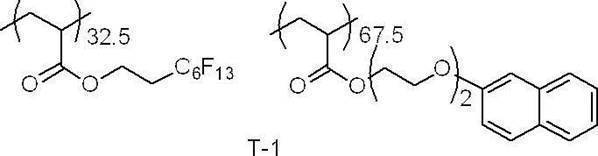
<比較例2>
厚みを調整した以外は、比較例1と同様の方法によって、位相差フィルムA-2を作製した。
厚みを調整した以外は、比較例1と同様の方法によって、位相差フィルムA-2を作製した。
<比較例3>
組成物A-1を下記の組成物A-2に変更し、厚みを調整した以外は、比較例1と同様の方法によって、位相差フィルムA-3を作製した。
――――――――――――――――――――――――――――――――――
組成物A-3
――――――――――――――――――――――――――――――――――
・液晶化合物L-1 50.00質量部
・液晶化合物L-2 50.00質量部
・重合開始剤PI-1 0.50質量部
・レベリング剤T-1 0.20質量部
・クロロホルム 560.00質量部
――――――――――――――――――――――――――――――――――
組成物A-1を下記の組成物A-2に変更し、厚みを調整した以外は、比較例1と同様の方法によって、位相差フィルムA-3を作製した。
――――――――――――――――――――――――――――――――――
組成物A-3
――――――――――――――――――――――――――――――――――
・液晶化合物L-1 50.00質量部
・液晶化合物L-2 50.00質量部
・重合開始剤PI-1 0.50質量部
・レベリング剤T-1 0.20質量部
・クロロホルム 560.00質量部
――――――――――――――――――――――――――――――――――
<実施例1>
組成物A-1に対し、下記二色性色素D-1(極大吸収波長:706nm/785nm)を14.00質量部加え、厚みを調整した以外は、実施例1と同様の方法によって、位相差フィルムA-4を作製した。
組成物A-1に対し、下記二色性色素D-1(極大吸収波長:706nm/785nm)を14.00質量部加え、厚みを調整した以外は、実施例1と同様の方法によって、位相差フィルムA-4を作製した。
二色性色素D-1
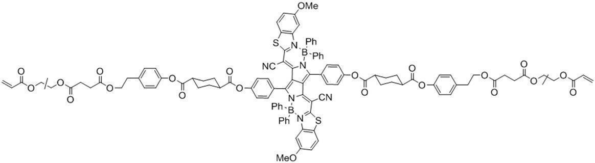
<実施例2>
組成物A-1に対し、上記二色性色素D-1を10.00質量部加え、厚みを調整した以外は、実施例1と同様の方法によって、位相差フィルムA-5を作製した。
組成物A-1に対し、上記二色性色素D-1を10.00質量部加え、厚みを調整した以外は、実施例1と同様の方法によって、位相差フィルムA-5を作製した。
<実施例3>
厚みを調整した以外は、実施例2と同様の方法によって、位相差フィルムA-6を作製した。
厚みを調整した以外は、実施例2と同様の方法によって、位相差フィルムA-6を作製した。
<実施例4>
組成物A-1に対し、上記二色性色素D-1を5.00質量部加え、厚みを調整した以外は、実施例1と同様の方法によって、位相差フィルムA-7を作製した。
組成物A-1に対し、上記二色性色素D-1を5.00質量部加え、厚みを調整した以外は、実施例1と同様の方法によって、位相差フィルムA-7を作製した。
<実施例5>
組成物A-1に対し、二色性色素G-241(極大吸収波長:555nm、長瀬産業製)を0.20質量部加え、厚みを調整した以外は、比較例1と同様の方法によって、位相差フィルムA-8を作製した。
組成物A-1に対し、二色性色素G-241(極大吸収波長:555nm、長瀬産業製)を0.20質量部加え、厚みを調整した以外は、比較例1と同様の方法によって、位相差フィルムA-8を作製した。
<比較例4>
組成物A-1に対し、二色性色素G-241(長瀬産業製)を0.70質量部加え、厚みを調整した以外は、比較例1と同様の方法によって、位相差フィルムA-9を作製した。
組成物A-1に対し、二色性色素G-241(長瀬産業製)を0.70質量部加え、厚みを調整した以外は、比較例1と同様の方法によって、位相差フィルムA-9を作製した。
<比較例5>
組成物A-1に対し、二色性色素M-137(極大吸収波長:582nm/621nm、三井化学ファイン社製)を0.20質量部加え、厚みを調整した以外は、比較例1と同様の方法によって、位相差フィルムA-10を作製した。
組成物A-1に対し、二色性色素M-137(極大吸収波長:582nm/621nm、三井化学ファイン社製)を0.20質量部加え、厚みを調整した以外は、比較例1と同様の方法によって、位相差フィルムA-10を作製した。
<比較例6>
組成物A-1に対し、二色性色素M-137(三井化学ファイン社製)を1.00質量部加え、厚みを調整した以外は、比較例1と同様の方法によって、位相差フィルムA-11を作製した。
組成物A-1に対し、二色性色素M-137(三井化学ファイン社製)を1.00質量部加え、厚みを調整した以外は、比較例1と同様の方法によって、位相差フィルムA-11を作製した。
<円偏光板の形成>
支持体であるTD80UL(富士フイルム社製)の表面を、アルカリ鹸化処理した。具体的には、上記支持体を1.5規定の水酸化ナトリウム水溶液に55℃で2分間浸漬し、取り出した支持体を室温の水洗浴槽中で洗浄し、30℃で0.1規定の硫酸を用いて中和した。その後、再度、得られた支持体を室温の水洗浴槽中で洗浄し、さらに100℃の温風で乾燥した。
続いて、ヨウ素水溶液中で厚み80μmのロール状ポリビニルアルコールフィルムを連続して5倍に延伸し、延伸後のフィルムを乾燥して、厚み20μmの偏光子を得た。
得られた偏光子と、アルカリ鹸化処理が施された支持体(TD80UL)とを貼りあわせ、片側に偏光子が露出した偏光板を得た。
次に、偏光子の吸収軸と実施例1~5、比較例1~6で作製した位相差フィルムA-1~A-11の遅相軸とのなす角度が45°となるように、偏光板中の偏光子と位相差フィルムの塗布面とを粘着剤を介して貼り合せ、続いてガラス基板を剥離し、位相差フィルムのみを偏光子上に転写し、円偏光板P-1~P-11を作製した。
支持体であるTD80UL(富士フイルム社製)の表面を、アルカリ鹸化処理した。具体的には、上記支持体を1.5規定の水酸化ナトリウム水溶液に55℃で2分間浸漬し、取り出した支持体を室温の水洗浴槽中で洗浄し、30℃で0.1規定の硫酸を用いて中和した。その後、再度、得られた支持体を室温の水洗浴槽中で洗浄し、さらに100℃の温風で乾燥した。
続いて、ヨウ素水溶液中で厚み80μmのロール状ポリビニルアルコールフィルムを連続して5倍に延伸し、延伸後のフィルムを乾燥して、厚み20μmの偏光子を得た。
得られた偏光子と、アルカリ鹸化処理が施された支持体(TD80UL)とを貼りあわせ、片側に偏光子が露出した偏光板を得た。
次に、偏光子の吸収軸と実施例1~5、比較例1~6で作製した位相差フィルムA-1~A-11の遅相軸とのなす角度が45°となるように、偏光板中の偏光子と位相差フィルムの塗布面とを粘着剤を介して貼り合せ、続いてガラス基板を剥離し、位相差フィルムのみを偏光子上に転写し、円偏光板P-1~P-11を作製した。
実施例1~5、比較例1~6で作製した位相差フィルムおよび円偏光板の各種評価結果を表1にまとめて示す。
<光学特性の測定>
AxoScan OPMF-1(オプトサイエンス社製)を用い、波長400~700nmの範囲において、面内レタデーションを測定した。
得られたデータを基にして、上述した要件2~9を満たすかどうかを判断した。
AxoScan OPMF-1(オプトサイエンス社製)を用い、波長400~700nmの範囲において、面内レタデーションを測定した。
得られたデータを基にして、上述した要件2~9を満たすかどうかを判断した。
<膜厚測定>
反射分光膜厚計FE3000(大塚電子株式会社製)を用いて、位相差フィルムの厚みを測定した。
反射分光膜厚計FE3000(大塚電子株式会社製)を用いて、位相差フィルムの厚みを測定した。
<フィルム色味測定>
上述した方法に従って、Δxyを算出した。
上述した方法に従って、Δxyを算出した。
(有機EL表示装置への実装)
有機EL表示パネル搭載のSAMSUNG社製GALAXY S IVを分解し、円偏光板を剥離して、円偏光板P-1~P-11をそれぞれ有機EL表示パネル上に貼合し、有機EL表示装置を作製した。
有機EL表示パネル搭載のSAMSUNG社製GALAXY S IVを分解し、円偏光板を剥離して、円偏光板P-1~P-11をそれぞれ有機EL表示パネル上に貼合し、有機EL表示装置を作製した。
<白表示色味の評価>
有機EL表示装置を点灯し、全領域に白を表示させた状態で、目視評価を行った。
A:色味づきが感じられない
B:色味づきがあるが、許容
C:色味づきが許容できない
有機EL表示装置を点灯し、全領域に白を表示させた状態で、目視評価を行った。
A:色味づきが感じられない
B:色味づきがあるが、許容
C:色味づきが許容できない
<反射防止性能の評価>
(反射率)
上記で得られた有機EL表示装置(電源オフ状態)に対して、測色計(コニカミノルタ製、CM-2022)を用い、SCE(Specular component excluded)モードで測定し、得られたY値を、比較例1の結果を基準として下記の基準で評価した。
A:比較例1でのY値に対し、Y値の割合が20%以下である場合
B:比較例1でのY値に対し、Y値の割合が20%超40%以下である場合
C:比較例1でのY値に対し、Y値の割合が40%超である場合
(反射率)
上記で得られた有機EL表示装置(電源オフ状態)に対して、測色計(コニカミノルタ製、CM-2022)を用い、SCE(Specular component excluded)モードで測定し、得られたY値を、比較例1の結果を基準として下記の基準で評価した。
A:比較例1でのY値に対し、Y値の割合が20%以下である場合
B:比較例1でのY値に対し、Y値の割合が20%超40%以下である場合
C:比較例1でのY値に対し、Y値の割合が40%超である場合
(反射色味)
上記で得られた有機EL表示装置(電源オフ状態)に対して、測色計(コニカミノルタ製、CM-2022)を用い、SCE(Specular component excluded)モードで測定し、得られた反射光のa*およびb*を用い、下記式で定義し、比較例1の結果を基準として下記の基準で評価した。
上記で得られた有機EL表示装置(電源オフ状態)に対して、測色計(コニカミノルタ製、CM-2022)を用い、SCE(Specular component excluded)モードで測定し、得られた反射光のa*およびb*を用い、下記式で定義し、比較例1の結果を基準として下記の基準で評価した。

A:比較例1での|ab|値に対し、|ab|の割合が70%未満である場合
B:比較例1での|ab|値に対し、|ab|の割合が70%以上100%未満である場合
C:比較例1での|ab|値に対し、|ab|の割合が100%以上150%未満である場合
D:比較例1での|ab|値に対し、|ab|の割合が150%以上である場合
B:比較例1での|ab|値に対し、|ab|の割合が70%以上100%未満である場合
C:比較例1での|ab|値に対し、|ab|の割合が100%以上150%未満である場合
D:比較例1での|ab|値に対し、|ab|の割合が150%以上である場合
表1中、「Re(550)」は、位相差フィルムの波長550nmにおける面内レタデーションを表す。
「色素」欄の「添加量」は、液晶化合物100質量部に対する、色素の使用量を表す。
「要件1(Δxy)」欄においては、Δxyの値を示す。
「要件2および3」欄においては、上述した要件2および3を満たす場合を「A」、要件2および3の少なくとも一方を満たさない場合を「B」として示す。
「要件4および5」欄においては、上述した要件4および5を満たす場合を「A」、要件4および5の少なくとも一方を満たさない場合を「B」として示す。
「要件6」欄においては、上述した要件6を満たす場合を「A」、要件6を満たさない場合を「B」として示す。
「要件7」欄においては、上述した要件7を満たす場合を「A」、要件7を満たさない場合を「B」として示す。
「要件8」欄においては、上述した要件8を満たす場合を「A」、要件8を満たさない場合を「B」として示す。
「要件9」欄においては、上述した要件9を満たす場合を「A」、要件9を満たさない場合を「B」として示す。
「要件10」欄においては、上述した要件10を満たす場合を「A」、要件10を満たさない場合を「B」として示す。
「要件11」欄においては、上述した要件11を満たす場合を「A」、要件11を満たさない場合を「B」として示す。
「色素」欄の「添加量」は、液晶化合物100質量部に対する、色素の使用量を表す。
「要件1(Δxy)」欄においては、Δxyの値を示す。
「要件2および3」欄においては、上述した要件2および3を満たす場合を「A」、要件2および3の少なくとも一方を満たさない場合を「B」として示す。
「要件4および5」欄においては、上述した要件4および5を満たす場合を「A」、要件4および5の少なくとも一方を満たさない場合を「B」として示す。
「要件6」欄においては、上述した要件6を満たす場合を「A」、要件6を満たさない場合を「B」として示す。
「要件7」欄においては、上述した要件7を満たす場合を「A」、要件7を満たさない場合を「B」として示す。
「要件8」欄においては、上述した要件8を満たす場合を「A」、要件8を満たさない場合を「B」として示す。
「要件9」欄においては、上述した要件9を満たす場合を「A」、要件9を満たさない場合を「B」として示す。
「要件10」欄においては、上述した要件10を満たす場合を「A」、要件10を満たさない場合を「B」として示す。
「要件11」欄においては、上述した要件11を満たす場合を「A」、要件11を満たさない場合を「B」として示す。

表1に示すように、本発明の位相差フィルムを用いると所望の効果が得られた。
なかでも、実施例1~5の比較から分かるように、要件4および5、要件7、並びに、要件9を満たす場合、より優れた効果が得られることが確認された。
なお、実施例1~5に関しては、要件12および要件13を満たすことも確認された。また、実施例1~3に関しては、要件14および要件15を満たすことも確認された。さらに、実施例1~5に関しては、波長450~500nmの範囲内の波長λ1における第1位相差フィルムの面内レタデーションRe(λ1)が上記要件2を満たし、波長600~650nmの範囲内の波長λ2における第1位相差フィルムの面内レタデーションRe(λ2)が上記要件3を満たすことも確認された。
なかでも、実施例1~5の比較から分かるように、要件4および5、要件7、並びに、要件9を満たす場合、より優れた効果が得られることが確認された。
なお、実施例1~5に関しては、要件12および要件13を満たすことも確認された。また、実施例1~3に関しては、要件14および要件15を満たすことも確認された。さらに、実施例1~5に関しては、波長450~500nmの範囲内の波長λ1における第1位相差フィルムの面内レタデーションRe(λ1)が上記要件2を満たし、波長600~650nmの範囲内の波長λ2における第1位相差フィルムの面内レタデーションRe(λ2)が上記要件3を満たすことも確認された。
Claims (8)
- 少なくとも液晶化合物を用いて形成された位相差フィルムであって、
波長550nmにおける面内レタデーションが100~200nmであり、
CIExy色度図上において、前記位相差フィルムに対して標準光源D65の光を入射させて得られる透過光の色度と、標準光源D65の色度との差であるΔxyが以下の要件1を満たし、
前記位相差フィルムに入射する測定光の波長を横軸に、波長450~600nmの範囲における25nm毎の前記測定光の波長における前記位相差フィルムの面内レタデーションを縦軸にプロットしたグラフにおいて、隣接する2つのプロット点を結ぶ直線の傾きSが、いずれも以下の要件6を満たす、位相差フィルム。
要件1:Δxy<0.010
ただし、Δxyは、以下式より算出される。
式:Δxy=((x-x0)2+(y-y0)2)1/2
xおよびyは前記位相差フィルムの透過光のCIExy色度図上の色度座標を表し、x0およびy0は標準光源D65のCIExy色度図上の色度座標を表す。
要件6:0.10<傾きS≦1.0 - 前記位相差フィルムに入射する測定光の波長を横軸に、波長450~650nmの範囲における25nm毎の前記測定光の波長における前記位相差フィルムの面内レタデーションを縦軸にプロットしたグラフにおいて、隣接する2つのプロット点を結ぶ直線の傾きSが、いずれも以下の要件7を満たす、請求項1に記載の位相差フィルム。
要件7:0.10<傾きS≦1.0 - 前記グラフにおいて、前記測定光が波長550nmであるプロット点と、前記測定光が波長575nmであるプロット点とを結んだ直線の傾きS(550)が以下の要件8を満たす、請求項1または2に記載の位相差フィルム。
要件8:0.10<傾きS(550)<0.20 - 前記グラフにおいて、前記測定光が波長625nmであるプロット点と、前記測定光が波長650nmであるプロット点とを結んだ直線の傾きS(625)が以下の要件9を満たす、請求項1~3のいずれか1項に記載の位相差フィルム。
要件9:0<|傾きS(625)-0.25|<0.15 - 少なくとも液晶化合物を用いて形成された位相差フィルムであって、
波長550nmにおける面内レタデーションが100~200nmであり、
CIExy色度図上において、前記位相差フィルムに対して標準光源D65の光を入射させて得られる透過光の色度と、標準光源D65の色度との差であるΔxyが以下の要件1を満たし、
前記位相差フィルムに入射する測定光の波長を横軸に、測定波長550nmにおける前記位相差フィルムの面内レタデーションを1.0として規格化した前記測定光の各波長における面内レタデーションを縦軸にプロットしたグラフにおいて、波長450~550nmの範囲内の波長λ1における前記位相差フィルムの面内レタデーションRe(λ1)が以下の要件10を満たし、波長550~650nmの範囲内の波長λ2における前記位相差フィルムの面内レタデーションRe(λ2)が以下の要件11を満たす、位相差フィルム。
要件1:Δxy<0.010
ただし、Δxyは、以下式より算出される。
式:Δxy=((x-x0)2+(y-y0)2)1/2
xおよびyは前記位相差フィルムの透過光のCIExy色度図上の色度座標を表し、x0およびy0は標準光源D65のCIExy色度図上の色度座標を表す。
要件10:0.0027×λ1-0.5≦Re(λ1)/Re(550)≦0.0014×λ1+0.25
要件11:0.0009×λ2+0.5≦Re(λ2)/Re(550)≦0.0023×λ2-0.25 - 前記液晶化合物が逆波長分散性を示す、請求項1~5のいずれか1項に記載の位相差フィルム。
- 偏光子と、請求項1~6のいずれか1項に記載の位相差フィルムとを含む、円偏光板。
- 有機エレクトロルミネッセンス表示パネルと、有機エレクトロルミネッセンス表示パネル上に配置された請求項7に記載の円偏光板と、を含む有機エレクトロルミネッセンス表示装置。
Priority Applications (2)
| Application Number | Priority Date | Filing Date | Title |
|---|---|---|---|
| JP2020555680A JP7239606B2 (ja) | 2018-11-13 | 2019-11-11 | 位相差フィルム、円偏光板、有機エレクトロルミネッセンス表示装置 |
| US17/313,330 US11997874B2 (en) | 2018-11-13 | 2021-05-06 | Phase difference film, circularly polarizing plate, and organic electroluminescent display device |
Applications Claiming Priority (2)
| Application Number | Priority Date | Filing Date | Title |
|---|---|---|---|
| JP2018212871 | 2018-11-13 | ||
| JP2018-212871 | 2018-11-13 |
Related Child Applications (1)
| Application Number | Title | Priority Date | Filing Date |
|---|---|---|---|
| US17/313,330 Continuation US11997874B2 (en) | 2018-11-13 | 2021-05-06 | Phase difference film, circularly polarizing plate, and organic electroluminescent display device |
Publications (1)
| Publication Number | Publication Date |
|---|---|
| WO2020100813A1 true WO2020100813A1 (ja) | 2020-05-22 |
Family
ID=70731814
Family Applications (1)
| Application Number | Title | Priority Date | Filing Date |
|---|---|---|---|
| PCT/JP2019/044142 Ceased WO2020100813A1 (ja) | 2018-11-13 | 2019-11-11 | 位相差フィルム、円偏光板、有機エレクトロルミネッセンス表示装置 |
Country Status (3)
| Country | Link |
|---|---|
| US (1) | US11997874B2 (ja) |
| JP (1) | JP7239606B2 (ja) |
| WO (1) | WO2020100813A1 (ja) |
Families Citing this family (1)
| Publication number | Priority date | Publication date | Assignee | Title |
|---|---|---|---|---|
| WO2021200987A1 (ja) * | 2020-03-30 | 2021-10-07 | 富士フイルム株式会社 | 光学異方性膜、円偏光板、表示装置 |
Citations (3)
| Publication number | Priority date | Publication date | Assignee | Title |
|---|---|---|---|---|
| JP2004070344A (ja) * | 2002-07-23 | 2004-03-04 | Nitto Denko Corp | 光学フィルムおよびそれを用いた液晶表示装置 |
| WO2010150693A1 (ja) * | 2009-06-25 | 2010-12-29 | チッソ株式会社 | 光配向した液晶性ポリイミドによる位相差膜及び光学素子 |
| US20140204460A1 (en) * | 2012-05-30 | 2014-07-24 | Lg Chem, Ltd | Polarizer, manufacturing method for the same and display device employing thereof |
Family Cites Families (5)
| Publication number | Priority date | Publication date | Assignee | Title |
|---|---|---|---|---|
| WO2000011516A1 (fr) * | 1998-08-25 | 2000-03-02 | Citizen Watch Co., Ltd. | Afficheur a cristaux liquide et son procede de fabrication |
| JP5103286B2 (ja) * | 2007-06-12 | 2012-12-19 | 富士フイルム株式会社 | バックライトユニット及び液晶表示装置 |
| JP5391682B2 (ja) | 2007-12-28 | 2014-01-15 | 住友化学株式会社 | 化合物、光学フィルム及び光学フィルムの製造方法 |
| JP5652011B2 (ja) * | 2010-06-10 | 2015-01-14 | 住友化学株式会社 | 光学フィルム |
| CN110058344A (zh) * | 2013-08-09 | 2019-07-26 | 住友化学株式会社 | 光学膜 |
-
2019
- 2019-11-11 WO PCT/JP2019/044142 patent/WO2020100813A1/ja not_active Ceased
- 2019-11-11 JP JP2020555680A patent/JP7239606B2/ja active Active
-
2021
- 2021-05-06 US US17/313,330 patent/US11997874B2/en active Active
Patent Citations (3)
| Publication number | Priority date | Publication date | Assignee | Title |
|---|---|---|---|---|
| JP2004070344A (ja) * | 2002-07-23 | 2004-03-04 | Nitto Denko Corp | 光学フィルムおよびそれを用いた液晶表示装置 |
| WO2010150693A1 (ja) * | 2009-06-25 | 2010-12-29 | チッソ株式会社 | 光配向した液晶性ポリイミドによる位相差膜及び光学素子 |
| US20140204460A1 (en) * | 2012-05-30 | 2014-07-24 | Lg Chem, Ltd | Polarizer, manufacturing method for the same and display device employing thereof |
Also Published As
| Publication number | Publication date |
|---|---|
| JPWO2020100813A1 (ja) | 2021-10-21 |
| US20210265595A1 (en) | 2021-08-26 |
| US11997874B2 (en) | 2024-05-28 |
| JP7239606B2 (ja) | 2023-03-14 |
Similar Documents
| Publication | Publication Date | Title |
|---|---|---|
| JP7034166B2 (ja) | 光学異方性膜、円偏光板、表示装置 | |
| CN110462868B (zh) | 有机电致发光显示装置、相位差薄膜、圆偏振片 | |
| JP6259925B2 (ja) | 円偏光板、表示装置 | |
| JP7351223B2 (ja) | 光学積層体、表示パネル及び表示装置 | |
| JP5723077B1 (ja) | 位相差板、楕円偏光板およびそれを用いた表示装置 | |
| JP2007279705A (ja) | 半透過型液晶表示装置 | |
| WO2019167926A1 (ja) | 積層体、有機電界発光装置、液晶表示装置 | |
| WO2019189809A1 (ja) | 光学素子および導光素子 | |
| JP7182686B2 (ja) | 光学異方性膜、積層体、円偏光板、表示装置 | |
| JP7171886B2 (ja) | 積層体、円偏光板、表示装置 | |
| JP2019204083A (ja) | 光学積層体、表示パネル及び表示装置 | |
| JP7192085B2 (ja) | 光学異方性膜、積層体、円偏光板、表示装置 | |
| WO2019151312A1 (ja) | 積層体 | |
| JP7158486B2 (ja) | 位相差フィルム、位相差フィルムの製造方法、偏光板および液晶表示装置 | |
| WO2019003812A1 (ja) | 光学異方性層及びその製造方法、光学異方性積層体、転写用複層物、偏光板、並びに画像表示装置 | |
| JP7239606B2 (ja) | 位相差フィルム、円偏光板、有機エレクトロルミネッセンス表示装置 | |
| US12505695B2 (en) | Fingerprint recognition sensor and optical element | |
| JP5269455B2 (ja) | 液晶表示装置 | |
| JP2016090866A (ja) | 光学フィルムの製造方法ならびにその方法により得られた光学フィルム、該光学フィルムを用いた楕円偏光板および画像表示装置 |
Legal Events
| Date | Code | Title | Description |
|---|---|---|---|
| 121 | Ep: the epo has been informed by wipo that ep was designated in this application |
Ref document number: 19884265 Country of ref document: EP Kind code of ref document: A1 |
|
| DPE1 | Request for preliminary examination filed after expiration of 19th month from priority date (pct application filed from 20040101) | ||
| ENP | Entry into the national phase |
Ref document number: 2020555680 Country of ref document: JP Kind code of ref document: A |
|
| NENP | Non-entry into the national phase |
Ref country code: DE |
|
| 122 | Ep: pct application non-entry in european phase |
Ref document number: 19884265 Country of ref document: EP Kind code of ref document: A1 |