WO2020085259A1 - 半導体装置製造方法 - Google Patents
半導体装置製造方法 Download PDFInfo
- Publication number
- WO2020085259A1 WO2020085259A1 PCT/JP2019/041202 JP2019041202W WO2020085259A1 WO 2020085259 A1 WO2020085259 A1 WO 2020085259A1 JP 2019041202 W JP2019041202 W JP 2019041202W WO 2020085259 A1 WO2020085259 A1 WO 2020085259A1
- Authority
- WO
- WIPO (PCT)
- Prior art keywords
- wafer
- group
- semiconductor device
- forming
- manufacturing
- Prior art date
- Legal status (The legal status is an assumption and is not a legal conclusion. Google has not performed a legal analysis and makes no representation as to the accuracy of the status listed.)
- Ceased
Links
Images








Classifications
-
- H—ELECTRICITY
- H10—SEMICONDUCTOR DEVICES; ELECTRIC SOLID-STATE DEVICES NOT OTHERWISE PROVIDED FOR
- H10P—GENERIC PROCESSES OR APPARATUS FOR THE MANUFACTURE OR TREATMENT OF DEVICES COVERED BY CLASS H10
- H10P72/00—Handling or holding of wafers, substrates or devices during manufacture or treatment thereof
- H10P72/70—Handling or holding of wafers, substrates or devices during manufacture or treatment thereof for supporting or gripping
- H10P72/74—Handling or holding of wafers, substrates or devices during manufacture or treatment thereof for supporting or gripping using temporarily an auxiliary support
-
- H—ELECTRICITY
- H10—SEMICONDUCTOR DEVICES; ELECTRIC SOLID-STATE DEVICES NOT OTHERWISE PROVIDED FOR
- H10W—GENERIC PACKAGES, INTERCONNECTIONS, CONNECTORS OR OTHER CONSTRUCTIONAL DETAILS OF DEVICES COVERED BY CLASS H10
- H10W20/00—Interconnections in chips, wafers or substrates
- H10W20/01—Manufacture or treatment
- H10W20/021—Manufacture or treatment of interconnections within wafers or substrates
- H10W20/023—Manufacture or treatment of interconnections within wafers or substrates the interconnections being through-semiconductor vias
-
- H—ELECTRICITY
- H10—SEMICONDUCTOR DEVICES; ELECTRIC SOLID-STATE DEVICES NOT OTHERWISE PROVIDED FOR
- H10W—GENERIC PACKAGES, INTERCONNECTIONS, CONNECTORS OR OTHER CONSTRUCTIONAL DETAILS OF DEVICES COVERED BY CLASS H10
- H10W20/00—Interconnections in chips, wafers or substrates
- H10W20/01—Manufacture or treatment
- H10W20/021—Manufacture or treatment of interconnections within wafers or substrates
- H10W20/023—Manufacture or treatment of interconnections within wafers or substrates the interconnections being through-semiconductor vias
- H10W20/0245—Manufacture or treatment of interconnections within wafers or substrates the interconnections being through-semiconductor vias comprising use of blind vias during the manufacture
-
- H—ELECTRICITY
- H10—SEMICONDUCTOR DEVICES; ELECTRIC SOLID-STATE DEVICES NOT OTHERWISE PROVIDED FOR
- H10W—GENERIC PACKAGES, INTERCONNECTIONS, CONNECTORS OR OTHER CONSTRUCTIONAL DETAILS OF DEVICES COVERED BY CLASS H10
- H10W20/00—Interconnections in chips, wafers or substrates
- H10W20/01—Manufacture or treatment
- H10W20/021—Manufacture or treatment of interconnections within wafers or substrates
- H10W20/023—Manufacture or treatment of interconnections within wafers or substrates the interconnections being through-semiconductor vias
- H10W20/0253—Manufacture or treatment of interconnections within wafers or substrates the interconnections being through-semiconductor vias comprising forming the through-semiconductor vias after stacking of the chips, wafers or substrates
-
- H—ELECTRICITY
- H10—SEMICONDUCTOR DEVICES; ELECTRIC SOLID-STATE DEVICES NOT OTHERWISE PROVIDED FOR
- H10W—GENERIC PACKAGES, INTERCONNECTIONS, CONNECTORS OR OTHER CONSTRUCTIONAL DETAILS OF DEVICES COVERED BY CLASS H10
- H10W20/00—Interconnections in chips, wafers or substrates
- H10W20/20—Interconnections within wafers or substrates, e.g. through-silicon vias [TSV]
- H10W20/211—Through-semiconductor vias, e.g. TSVs
- H10W20/212—Top-view shapes or dispositions, e.g. top-view layouts of the vias
- H10W20/2125—Top-view shapes
-
- H—ELECTRICITY
- H10—SEMICONDUCTOR DEVICES; ELECTRIC SOLID-STATE DEVICES NOT OTHERWISE PROVIDED FOR
- H10W—GENERIC PACKAGES, INTERCONNECTIONS, CONNECTORS OR OTHER CONSTRUCTIONAL DETAILS OF DEVICES COVERED BY CLASS H10
- H10W72/00—Interconnections or connectors in packages
- H10W72/90—Bond pads, in general
-
- H—ELECTRICITY
- H10—SEMICONDUCTOR DEVICES; ELECTRIC SOLID-STATE DEVICES NOT OTHERWISE PROVIDED FOR
- H10W—GENERIC PACKAGES, INTERCONNECTIONS, CONNECTORS OR OTHER CONSTRUCTIONAL DETAILS OF DEVICES COVERED BY CLASS H10
- H10W80/00—Direct bonding of chips, wafers or substrates
-
- H—ELECTRICITY
- H10—SEMICONDUCTOR DEVICES; ELECTRIC SOLID-STATE DEVICES NOT OTHERWISE PROVIDED FOR
- H10W—GENERIC PACKAGES, INTERCONNECTIONS, CONNECTORS OR OTHER CONSTRUCTIONAL DETAILS OF DEVICES COVERED BY CLASS H10
- H10W90/00—Package configurations
-
- H—ELECTRICITY
- H10—SEMICONDUCTOR DEVICES; ELECTRIC SOLID-STATE DEVICES NOT OTHERWISE PROVIDED FOR
- H10W—GENERIC PACKAGES, INTERCONNECTIONS, CONNECTORS OR OTHER CONSTRUCTIONAL DETAILS OF DEVICES COVERED BY CLASS H10
- H10W99/00—Subject matter not provided for in other groups of this subclass
-
- H—ELECTRICITY
- H10—SEMICONDUCTOR DEVICES; ELECTRIC SOLID-STATE DEVICES NOT OTHERWISE PROVIDED FOR
- H10P—GENERIC PROCESSES OR APPARATUS FOR THE MANUFACTURE OR TREATMENT OF DEVICES COVERED BY CLASS H10
- H10P52/00—Grinding, lapping or polishing of wafers, substrates or parts of devices
-
- H—ELECTRICITY
- H10—SEMICONDUCTOR DEVICES; ELECTRIC SOLID-STATE DEVICES NOT OTHERWISE PROVIDED FOR
- H10P—GENERIC PROCESSES OR APPARATUS FOR THE MANUFACTURE OR TREATMENT OF DEVICES COVERED BY CLASS H10
- H10P72/00—Handling or holding of wafers, substrates or devices during manufacture or treatment thereof
- H10P72/70—Handling or holding of wafers, substrates or devices during manufacture or treatment thereof for supporting or gripping
- H10P72/74—Handling or holding of wafers, substrates or devices during manufacture or treatment thereof for supporting or gripping using temporarily an auxiliary support
- H10P72/7416—Handling or holding of wafers, substrates or devices during manufacture or treatment thereof for supporting or gripping using temporarily an auxiliary support used during dicing or grinding
-
- H—ELECTRICITY
- H10—SEMICONDUCTOR DEVICES; ELECTRIC SOLID-STATE DEVICES NOT OTHERWISE PROVIDED FOR
- H10W—GENERIC PACKAGES, INTERCONNECTIONS, CONNECTORS OR OTHER CONSTRUCTIONAL DETAILS OF DEVICES COVERED BY CLASS H10
- H10W70/00—Package substrates; Interposers; Redistribution layers [RDL]
- H10W70/01—Manufacture or treatment
- H10W70/05—Manufacture or treatment of insulating or insulated package substrates, or of interposers, or of redistribution layers
- H10W70/093—Connecting or disconnecting other interconnections thereto or therefrom, e.g. connecting bond wires or bumps
-
- H—ELECTRICITY
- H10—SEMICONDUCTOR DEVICES; ELECTRIC SOLID-STATE DEVICES NOT OTHERWISE PROVIDED FOR
- H10W—GENERIC PACKAGES, INTERCONNECTIONS, CONNECTORS OR OTHER CONSTRUCTIONAL DETAILS OF DEVICES COVERED BY CLASS H10
- H10W70/00—Package substrates; Interposers; Redistribution layers [RDL]
- H10W70/60—Insulating or insulated package substrates; Interposers; Redistribution layers
-
- H—ELECTRICITY
- H10—SEMICONDUCTOR DEVICES; ELECTRIC SOLID-STATE DEVICES NOT OTHERWISE PROVIDED FOR
- H10W—GENERIC PACKAGES, INTERCONNECTIONS, CONNECTORS OR OTHER CONSTRUCTIONAL DETAILS OF DEVICES COVERED BY CLASS H10
- H10W72/00—Interconnections or connectors in packages
- H10W72/01—Manufacture or treatment
- H10W72/013—Manufacture or treatment of die-attach connectors
- H10W72/01331—Manufacture or treatment of die-attach connectors using blanket deposition
- H10W72/01333—Manufacture or treatment of die-attach connectors using blanket deposition in liquid form, e.g. spin coating, spray coating or immersion coating
-
- H—ELECTRICITY
- H10—SEMICONDUCTOR DEVICES; ELECTRIC SOLID-STATE DEVICES NOT OTHERWISE PROVIDED FOR
- H10W—GENERIC PACKAGES, INTERCONNECTIONS, CONNECTORS OR OTHER CONSTRUCTIONAL DETAILS OF DEVICES COVERED BY CLASS H10
- H10W72/00—Interconnections or connectors in packages
- H10W72/01—Manufacture or treatment
- H10W72/013—Manufacture or treatment of die-attach connectors
- H10W72/01365—Thermally treating
-
- H—ELECTRICITY
- H10—SEMICONDUCTOR DEVICES; ELECTRIC SOLID-STATE DEVICES NOT OTHERWISE PROVIDED FOR
- H10W—GENERIC PACKAGES, INTERCONNECTIONS, CONNECTORS OR OTHER CONSTRUCTIONAL DETAILS OF DEVICES COVERED BY CLASS H10
- H10W72/00—Interconnections or connectors in packages
- H10W72/01—Manufacture or treatment
- H10W72/013—Manufacture or treatment of die-attach connectors
- H10W72/01371—Cleaning, e.g. oxide removal or de-smearing
-
- H—ELECTRICITY
- H10—SEMICONDUCTOR DEVICES; ELECTRIC SOLID-STATE DEVICES NOT OTHERWISE PROVIDED FOR
- H10W—GENERIC PACKAGES, INTERCONNECTIONS, CONNECTORS OR OTHER CONSTRUCTIONAL DETAILS OF DEVICES COVERED BY CLASS H10
- H10W72/00—Interconnections or connectors in packages
- H10W72/01—Manufacture or treatment
- H10W72/0198—Manufacture or treatment batch processes
-
- H—ELECTRICITY
- H10—SEMICONDUCTOR DEVICES; ELECTRIC SOLID-STATE DEVICES NOT OTHERWISE PROVIDED FOR
- H10W—GENERIC PACKAGES, INTERCONNECTIONS, CONNECTORS OR OTHER CONSTRUCTIONAL DETAILS OF DEVICES COVERED BY CLASS H10
- H10W72/00—Interconnections or connectors in packages
- H10W72/071—Connecting or disconnecting
- H10W72/073—Connecting or disconnecting of die-attach connectors
-
- H—ELECTRICITY
- H10—SEMICONDUCTOR DEVICES; ELECTRIC SOLID-STATE DEVICES NOT OTHERWISE PROVIDED FOR
- H10W—GENERIC PACKAGES, INTERCONNECTIONS, CONNECTORS OR OTHER CONSTRUCTIONAL DETAILS OF DEVICES COVERED BY CLASS H10
- H10W72/00—Interconnections or connectors in packages
- H10W72/071—Connecting or disconnecting
- H10W72/073—Connecting or disconnecting of die-attach connectors
- H10W72/07302—Connecting or disconnecting of die-attach connectors using an auxiliary member
- H10W72/07304—Connecting or disconnecting of die-attach connectors using an auxiliary member the auxiliary member being temporary, e.g. a sacrificial coating
- H10W72/07307—Connecting or disconnecting of die-attach connectors using an auxiliary member the auxiliary member being temporary, e.g. a sacrificial coating the auxiliary member being a temporary substrate, e.g. a removable substrate
-
- H—ELECTRICITY
- H10—SEMICONDUCTOR DEVICES; ELECTRIC SOLID-STATE DEVICES NOT OTHERWISE PROVIDED FOR
- H10W—GENERIC PACKAGES, INTERCONNECTIONS, CONNECTORS OR OTHER CONSTRUCTIONAL DETAILS OF DEVICES COVERED BY CLASS H10
- H10W72/00—Interconnections or connectors in packages
- H10W72/071—Connecting or disconnecting
- H10W72/073—Connecting or disconnecting of die-attach connectors
- H10W72/07311—Treating the bonding area before connecting, e.g. by applying flux or cleaning
-
- H—ELECTRICITY
- H10—SEMICONDUCTOR DEVICES; ELECTRIC SOLID-STATE DEVICES NOT OTHERWISE PROVIDED FOR
- H10W—GENERIC PACKAGES, INTERCONNECTIONS, CONNECTORS OR OTHER CONSTRUCTIONAL DETAILS OF DEVICES COVERED BY CLASS H10
- H10W72/00—Interconnections or connectors in packages
- H10W72/071—Connecting or disconnecting
- H10W72/073—Connecting or disconnecting of die-attach connectors
- H10W72/07331—Connecting techniques
-
- H—ELECTRICITY
- H10—SEMICONDUCTOR DEVICES; ELECTRIC SOLID-STATE DEVICES NOT OTHERWISE PROVIDED FOR
- H10W—GENERIC PACKAGES, INTERCONNECTIONS, CONNECTORS OR OTHER CONSTRUCTIONAL DETAILS OF DEVICES COVERED BY CLASS H10
- H10W72/00—Interconnections or connectors in packages
- H10W72/071—Connecting or disconnecting
- H10W72/073—Connecting or disconnecting of die-attach connectors
- H10W72/07331—Connecting techniques
- H10W72/07332—Compression bonding, e.g. thermocompression bonding
-
- H—ELECTRICITY
- H10—SEMICONDUCTOR DEVICES; ELECTRIC SOLID-STATE DEVICES NOT OTHERWISE PROVIDED FOR
- H10W—GENERIC PACKAGES, INTERCONNECTIONS, CONNECTORS OR OTHER CONSTRUCTIONAL DETAILS OF DEVICES COVERED BY CLASS H10
- H10W72/00—Interconnections or connectors in packages
- H10W72/071—Connecting or disconnecting
- H10W72/073—Connecting or disconnecting of die-attach connectors
- H10W72/07331—Connecting techniques
- H10W72/07337—Connecting techniques using a polymer adhesive, e.g. an adhesive based on silicone or epoxy
- H10W72/07338—Connecting techniques using a polymer adhesive, e.g. an adhesive based on silicone or epoxy hardening the adhesive by curing, e.g. thermosetting
-
- H—ELECTRICITY
- H10—SEMICONDUCTOR DEVICES; ELECTRIC SOLID-STATE DEVICES NOT OTHERWISE PROVIDED FOR
- H10W—GENERIC PACKAGES, INTERCONNECTIONS, CONNECTORS OR OTHER CONSTRUCTIONAL DETAILS OF DEVICES COVERED BY CLASS H10
- H10W72/00—Interconnections or connectors in packages
- H10W72/071—Connecting or disconnecting
- H10W72/073—Connecting or disconnecting of die-attach connectors
- H10W72/07351—Connecting or disconnecting of die-attach connectors characterised by changes in properties of the die-attach connectors during connecting
- H10W72/07354—Connecting or disconnecting of die-attach connectors characterised by changes in properties of the die-attach connectors during connecting changes in dispositions
-
- H—ELECTRICITY
- H10—SEMICONDUCTOR DEVICES; ELECTRIC SOLID-STATE DEVICES NOT OTHERWISE PROVIDED FOR
- H10W—GENERIC PACKAGES, INTERCONNECTIONS, CONNECTORS OR OTHER CONSTRUCTIONAL DETAILS OF DEVICES COVERED BY CLASS H10
- H10W72/00—Interconnections or connectors in packages
- H10W72/30—Die-attach connectors
- H10W72/341—Dispositions of die-attach connectors, e.g. layouts
- H10W72/347—Dispositions of multiple die-attach connectors
-
- H—ELECTRICITY
- H10—SEMICONDUCTOR DEVICES; ELECTRIC SOLID-STATE DEVICES NOT OTHERWISE PROVIDED FOR
- H10W—GENERIC PACKAGES, INTERCONNECTIONS, CONNECTORS OR OTHER CONSTRUCTIONAL DETAILS OF DEVICES COVERED BY CLASS H10
- H10W72/00—Interconnections or connectors in packages
- H10W72/30—Die-attach connectors
- H10W72/351—Materials of die-attach connectors
- H10W72/353—Materials of die-attach connectors not comprising solid metals or solid metalloids, e.g. ceramics
- H10W72/354—Materials of die-attach connectors not comprising solid metals or solid metalloids, e.g. ceramics comprising polymers
-
- H—ELECTRICITY
- H10—SEMICONDUCTOR DEVICES; ELECTRIC SOLID-STATE DEVICES NOT OTHERWISE PROVIDED FOR
- H10W—GENERIC PACKAGES, INTERCONNECTIONS, CONNECTORS OR OTHER CONSTRUCTIONAL DETAILS OF DEVICES COVERED BY CLASS H10
- H10W80/00—Direct bonding of chips, wafers or substrates
- H10W80/301—Bonding techniques, e.g. hybrid bonding
- H10W80/312—Bonding techniques, e.g. hybrid bonding characterised by the direct bonding of electrically conductive pads
-
- H—ELECTRICITY
- H10—SEMICONDUCTOR DEVICES; ELECTRIC SOLID-STATE DEVICES NOT OTHERWISE PROVIDED FOR
- H10W—GENERIC PACKAGES, INTERCONNECTIONS, CONNECTORS OR OTHER CONSTRUCTIONAL DETAILS OF DEVICES COVERED BY CLASS H10
- H10W80/00—Direct bonding of chips, wafers or substrates
- H10W80/301—Bonding techniques, e.g. hybrid bonding
- H10W80/327—Bonding techniques, e.g. hybrid bonding characterised by the direct bonding of insulating parts, e.g. of silicon oxide layers
-
- H—ELECTRICITY
- H10—SEMICONDUCTOR DEVICES; ELECTRIC SOLID-STATE DEVICES NOT OTHERWISE PROVIDED FOR
- H10W—GENERIC PACKAGES, INTERCONNECTIONS, CONNECTORS OR OTHER CONSTRUCTIONAL DETAILS OF DEVICES COVERED BY CLASS H10
- H10W90/00—Package configurations
- H10W90/20—Configurations of stacked chips
- H10W90/22—Configurations of stacked chips the stacked chips being on both top and bottom sides of a package substrate, interposer or RDL
-
- H—ELECTRICITY
- H10—SEMICONDUCTOR DEVICES; ELECTRIC SOLID-STATE DEVICES NOT OTHERWISE PROVIDED FOR
- H10W—GENERIC PACKAGES, INTERCONNECTIONS, CONNECTORS OR OTHER CONSTRUCTIONAL DETAILS OF DEVICES COVERED BY CLASS H10
- H10W90/00—Package configurations
- H10W90/20—Configurations of stacked chips
- H10W90/297—Configurations of stacked chips characterised by the through-semiconductor vias [TSVs] in the stacked chips
-
- H—ELECTRICITY
- H10—SEMICONDUCTOR DEVICES; ELECTRIC SOLID-STATE DEVICES NOT OTHERWISE PROVIDED FOR
- H10W—GENERIC PACKAGES, INTERCONNECTIONS, CONNECTORS OR OTHER CONSTRUCTIONAL DETAILS OF DEVICES COVERED BY CLASS H10
- H10W90/00—Package configurations
- H10W90/701—Package configurations characterised by the relative positions of pads or connectors relative to package parts
- H10W90/721—Package configurations characterised by the relative positions of pads or connectors relative to package parts of bump connectors
- H10W90/722—Package configurations characterised by the relative positions of pads or connectors relative to package parts of bump connectors between stacked chips
-
- H—ELECTRICITY
- H10—SEMICONDUCTOR DEVICES; ELECTRIC SOLID-STATE DEVICES NOT OTHERWISE PROVIDED FOR
- H10W—GENERIC PACKAGES, INTERCONNECTIONS, CONNECTORS OR OTHER CONSTRUCTIONAL DETAILS OF DEVICES COVERED BY CLASS H10
- H10W90/00—Package configurations
- H10W90/701—Package configurations characterised by the relative positions of pads or connectors relative to package parts
- H10W90/731—Package configurations characterised by the relative positions of pads or connectors relative to package parts of die-attach connectors
- H10W90/732—Package configurations characterised by the relative positions of pads or connectors relative to package parts of die-attach connectors between stacked chips
-
- H—ELECTRICITY
- H10—SEMICONDUCTOR DEVICES; ELECTRIC SOLID-STATE DEVICES NOT OTHERWISE PROVIDED FOR
- H10W—GENERIC PACKAGES, INTERCONNECTIONS, CONNECTORS OR OTHER CONSTRUCTIONAL DETAILS OF DEVICES COVERED BY CLASS H10
- H10W90/00—Package configurations
- H10W90/701—Package configurations characterised by the relative positions of pads or connectors relative to package parts
- H10W90/791—Package configurations characterised by the relative positions of pads or connectors relative to package parts of direct-bonded pads
- H10W90/792—Package configurations characterised by the relative positions of pads or connectors relative to package parts of direct-bonded pads between multiple chips
Definitions
- the present invention relates to a method for manufacturing a semiconductor device having a laminated structure including a plurality of semiconductor elements.
- the present application claims the priority of Japanese Patent Application No. 2018-199013 filed in Japan on October 23, 2018, and the content thereof is incorporated herein.
- so-called through electrodes are formed to electrically connect semiconductor elements between different semiconductor wafers. For example, each time a next wafer is stacked on the lower wafer in the wafer stacking process, an electrode penetrating the stacked wafer in the thickness direction is formed to electrically connect the semiconductor elements between the two wafers.
- a series of steps for forming a through electrode for example, formation of a through opening in a laminated wafer, formation of an insulating film on the inner wall surface of the opening, and conduction in the opening are performed. It is not efficient because it is necessary to carry out the filling of the material, the various kinds of cleaning treatments associated therewith, etc. for each laminated wafer.
- the openings of the wafer stacked body are extended over the plurality of wafers in the thickness direction. It is also known to perform a series of steps including formation of a through electrode to form a through electrode for electrically connecting semiconductor elements between the wafers.
- a through electrode to form a through electrode for electrically connecting semiconductor elements between the wafers.
- the present invention has been devised under the circumstances as described above, and an object thereof is to provide a semiconductor device manufacturing method in which semiconductor elements are multi-layered by stacking wafers in which semiconductor elements are formed.
- the object is to provide a method suitable for efficiently manufacturing a semiconductor device while realizing a large number of stacked wafers.
- the semiconductor device manufacturing method provided by the present invention includes the following wafer laminated body forming step, electrode forming step, electrode edge exposing step, and multilayering step.
- Each wafer stack includes a plurality of wafers each having an element formation surface and a back surface opposite to the element formation surface in an orientation in which the element formation surface of one wafer and the back surface of the other wafer face each other in two adjacent wafers.
- a wafer (first wafer) located at one end in the stacking direction of the wafer stack has an adjacent wafer located on the back surface side thereof and a wafer (second wafer) located at the other end in the stacking direction of the wafer stack.
- the adjacent wafer is located on the element forming surface side of the wafer.
- the element forming surface of the wafer is a surface on which a plurality of semiconductor elements are formed through a transistor forming step, a wiring forming step, and the like.
- the number of stacked wafers may be the same or different between the stacked wafers.
- the electrode forming step at least one through electrode is formed on each wafer laminated body.
- the through electrode extends from the element formation surface side of the first wafer in the wafer stack to a position beyond the element formation surface of the second wafer in the wafer stack.
- This step is preferably a step of forming an opening extending from the element formation surface side of the first wafer to a position beyond the element formation surface of the second wafer in the wafer stack, and filling the opening with a conductive material. And a step of performing.
- the second wafer is thinned by grinding the back surface of the second wafer in each wafer laminated body that has undergone the electrode forming step to expose the through electrode on the back surface.
- the element formation surface side of the first wafer in one wafer stack that is the bonding target and the element formation surface side of the first wafer in the other wafer stack may be bonded.
- bonding between the element formation surface side of the first wafer in one of the wafer stacks to be bonded and the back surface side of the second wafer in the other wafer stack may be performed (wafer. Face-to-back joining between laminates).
- the back surface side of the second wafer in one of the wafer stacks to be bonded and the back surface side of the second wafer in the other wafer stack may be bonded (wafer stack). Back-to-back joint between).
- a through electrode extending over a plurality of wafers included in each wafer laminated body to be joined to another wafer laminated body in a later multilayering step is formed.
- Such a configuration has a series of steps for forming a through electrode for each wafer in the process of forming a wafer laminated body (that is, forming an opening penetrating one wafer and forming an opening on the inner wall surface of the opening). It is suitable for avoiding or reducing the formation of the insulating film, the filling of the conductive material into the opening, and the various kinds of cleaning treatments associated therewith, and the efficient manufacture of the semiconductor device in the WOW process.
- the through holes are electrically connected between at least two wafer stacked bodies in which the through electrodes are already formed, and the wafer stacked bodies are joined together to form a wafer. It is further multi-layered. Such a configuration is suitable for realizing a large number of stacked wafers in the WOW process.
- the present semiconductor device manufacturing method it is not necessary to form electrodes that collectively penetrate the wafer laminated body in the number of laminated layers corresponding to the number of semiconductor element laminated layers of the semiconductor device to be manufactured.
- the present semiconductor device manufacturing method as described above is suitable for avoiding or suppressing the above-described difficulties associated with the formation of the collective through electrode.
- the present semiconductor device manufacturing method is capable of efficiently manufacturing a semiconductor device while avoiding or suppressing the difficulty of forming the through electrode due to the increase in the number of wafer stacked bodies and realizing a large number of stacked wafers. It is suitable.
- the through electrode forming method in the above electrode forming step when the method described in, for example, Japanese Patent Laid-Open No. 2016-4835 is adopted as the through electrode forming method in the above electrode forming step, the density of semiconductor elements on each wafer is increased.
- the partial conductive portions formed in each wafer which form continuous through electrodes in series, have different cross-sectional areas between adjacent wafers (cross-sectional area in the in-plane direction of the wafer). The cross-sectional area of the partial conductive portion is inevitably gradually increased for each wafer as the number of stacked wafers increases.
- the present semiconductor device manufacturing method is suitable for increasing the number of stacked wafers and increasing the density of semiconductor elements on each wafer.
- the wafer laminated body forming step includes a step of bonding the wafer to an element forming surface side of a base wafer having an element forming surface and a back surface opposite to the element forming surface, and grinding the wafer to form a wafer on the base wafer. It includes a step of forming a thinned wafer and a step of forming a semiconductor element on the surface to be ground of the thinned wafer.
- Such a wafer laminated body forming step includes a step of bonding the wafer to the element formation surface side of the thinned wafer on the base wafer, a step of forming the thinned wafer on the base wafer by grinding the wafer, The method may further include the step of forming a semiconductor element on the surface to be ground of the patterned wafer.
- the wafer laminated body forming step includes the following preparing step, thinning step, joining step, and removing step.
- a reinforcement wafer is prepared.
- the reinforcing wafer has a laminated structure including a wafer having an element formation surface and a back surface opposite to the element formation surface, a support substrate, and a temporary adhesive layer between the element formation surface side of the wafer and the support substrate.
- the temporary adhesive layer is for realizing a temporary adhesion state between the support substrate and the wafer.
- the wafer in such a reinforced wafer is thinned by grinding from the back surface side.
- the thinned wafer is formed while being supported by the supporting substrate.
- the element forming surface side of the base wafer having the element forming surface and the back surface opposite to this and the back surface side of the above-mentioned thinned wafer of the reinforcing wafer are bonded via an adhesive.
- the main joining step preferably includes a curing treatment for curing the adhesive at a temperature lower than the softening point of the polymer in the temporary adhesive layer.
- an adhesive is applied to one or both of the joining target surfaces (element forming surface of the base wafer, back surface of the thinned wafer), and the joining target surfaces are bonded via the adhesive, After the bonding, the adhesive is cured.
- one or both of the surfaces to be bonded may be treated with a silane coupling agent before applying the adhesive.
- the removal step the temporary adhesion state of the temporary adhesive layer between the supporting substrate and the thinned wafer in the reinforced wafer that has undergone the above-described bonding step is released, and the supporting substrate is removed.
- the removing step preferably includes a softening treatment for softening the temporary adhesive layer at a temperature higher than the softening point of the polymer in the temporary adhesive layer.
- the wafer stack forming process including the preparation process, the thinning process, the bonding process, and the removing process as described above is suitable for forming a thin wafer stack in which semiconductor elements are built.
- the wafer laminated body forming step includes a step of preparing at least one additional reinforcing wafer, a thinning step for each additional reinforcing wafer, and an additional joining step for each additional reinforcing wafer. It may further include a removing step after the additional joining step.
- the additional reinforcing wafer has a laminated structure including a wafer having an element formation surface and a back surface opposite to the element formation surface, a support substrate, and a temporary adhesive layer between the element formation surface side of the wafer and the support substrate. In the thinning process for each additional reinforcing wafer, the wafer in such an additional reinforcing wafer is ground from the back surface side to form a thinning wafer.
- the back surface side of the thinned wafer in the additional reinforcing wafer is bonded to the element formation surface side of the thinned wafer on the base wafer via an adhesive.
- the thinned wafer on the base wafer is a thinned wafer bonded to the base wafer in the above-described bonding process, or a thinned wafer additionally stacked on the thinned wafer in the preceding additional bonding process.
- This step preferably includes a curing treatment for curing the adhesive at a temperature lower than the softening point of the polymer in the temporary adhesive layer.
- an adhesive is applied to one or both of the surfaces to be bonded (element forming surface of one thinned wafer, rear surface of the other thinned wafer), and the adhesive is applied via the adhesive.
- the surfaces to be joined are pasted together, and the adhesive is cured after the pasting.
- a silane coupling agent treatment may be applied to one or both of the joining target surfaces before the application of the adhesive.
- the removal step after the additional bonding step the temporary adhesion state of the additional reinforcing wafer between the support substrate and the thinned wafer by the temporary adhesive layer is released, and the support substrate is removed.
- This step preferably includes a softening treatment for softening the temporary adhesive layer at a temperature higher than the softening point of the polymer in the temporary adhesive layer. It is suitable for further layering a thin wafer having semiconductor elements built therein.
- the temporary adhesive for forming the temporary adhesive layer in the reinforced wafer is preferably a polyvalent vinyl ether compound and two hydroxy groups or carboxy groups capable of reacting with the vinyl ether group to form an acetal bond. It contains a compound having the above and capable of forming a polymer with the polyvalent vinyl ether compound, and a thermoplastic resin.
- the above-mentioned adhesive used in the bonding step preferably contains a polyorganosilsesquioxane having a polymerizable functional group (that is, a polyorganosilsesquioxane containing a polymerizable group).
- the polymerizable group-containing polyorganosilsesquioxane is suitable for achieving a relatively low polymerization temperature or curing temperature of, for example, about 30 to 200 ° C. and also for achieving high heat resistance after curing. Therefore, the adhesive bonding between wafers by the adhesive containing the polymerizable group-containing polyorganosilsesquioxane realizes high heat resistance in the adhesive layer formed between the wafers, and the curing temperature for forming the adhesive layer. Is suitable for suppressing damage to the elements in the wafer as the adherend by reducing
- the temporary adhesive layer in the reinforced wafer used in the bonding step is suitable for achieving a relatively high softening temperature as described above, and the adhesive (polymerizable group-containing polyorganosilsesqui) used in the same step is used.
- the oxane-containing adhesive is suitable for achieving a relatively low curing temperature and high heat resistance after curing.
- Such a composite functional configuration is suitable for achieving both the joining process and the subsequent removing process.
- the bonding step is performed under a relatively low temperature condition, and the adhesive bonding of the thinned wafer to the base wafer is performed well while maintaining the temporary bonding state between the supporting substrate and the thinned wafer in the reinforcing wafer.
- the subsequent removal process is performed at relatively high temperature conditions to soften the temporary adhesive layer while maintaining the adhesive bond between the base wafer and the thinned wafer, Suitable for carrying out the removal of the supporting substrate.
- the above-described composite structure in the second preferred embodiment of the wafer laminated body forming step is suitable for forming a wafer laminated body so as to form a thin wafer into multiple layers through adhesive bonding while avoiding wafer breakage.
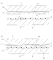
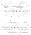
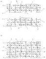
- 3 shows some steps in the semiconductor device manufacturing method according to the embodiment of the present invention.
- 3 shows some steps in the semiconductor device manufacturing method according to the embodiment of the present invention.
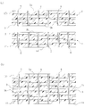
- 3 shows some steps in the semiconductor device manufacturing method according to the embodiment of the present invention.
- 3 shows some steps in the semiconductor device manufacturing method according to the embodiment of the present invention.
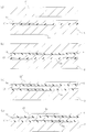
- 3 shows some steps in the semiconductor device manufacturing method according to the embodiment of the present invention.
- 3 shows some steps in the semiconductor device manufacturing method according to the embodiment of the present invention.
- 3 shows some steps in the semiconductor device manufacturing method according to the embodiment of the present invention.
- 3 shows some steps in the semiconductor device manufacturing method according to the embodiment of the present invention.
- 3 shows some steps in the semiconductor device manufacturing method according to the embodiment of the present invention.
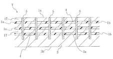
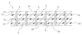
- FIG. 3 shows some steps in the semiconductor device manufacturing method according to the embodiment of the present invention. 3 shows some steps in the semiconductor device manufacturing method according to the embodiment of the present invention. An example of a through electrode forming step is shown. An example of a wafer laminated body formation process is represented. 14 shows the step that follows FIG. 14.
- FIGS. 1 to 12 show a semiconductor device manufacturing method according to an embodiment of the present invention.
- This manufacturing method is a method for manufacturing a semiconductor device having a three-dimensional structure in which semiconductor elements are integrated in the thickness direction, and FIGS. 1 to 12 are partial cross-sectional views showing the manufacturing process.
- a reinforcing wafer 1R as shown in FIG. 1A is prepared (preparation process).
- the reinforcing wafer 1R has a laminated structure including the wafer 1, the supporting substrate S, and the temporary adhesive layer 2 between them.
- the wafer 1 is a wafer having a semiconductor wafer body into which semiconductor elements can be formed, and has an element forming surface 1a and a back surface 1b opposite thereto.
- the element formation surface of the wafer is a surface on which a plurality of semiconductor elements (not shown) are formed on the wafer through a transistor formation process, a wiring formation process, and the like.
- Each semiconductor element of the wafer 1 has, for example, a multilayer wiring structure portion including exposed electrode pads on its surface.
- the wafer 1 has various semiconductor elements already formed on the element forming surface 1a side, and the wiring structure required for the semiconductor element is formed later on the element forming surface 1a. May be.
- constituent materials for forming the semiconductor wafer body of the wafer 1 include silicon (Si), germanium (Ge), silicon carbide (SiC), gallium arsenide (GaAs), gallium nitride (GaN), and indium phosphide (InP). ) Is mentioned.
- the thickness of such a wafer 1 is preferably 1000 ⁇ m or less, more preferably 900 ⁇ m or less, and still more preferably 800 ⁇ m or less from the viewpoint of shortening the grinding time in the grinding process described later.
- the thickness of the wafer 1 is, for example, 500 ⁇ m or more.
- the supporting substrate S in the reinforcing wafer 1R is for reinforcing the wafer 1 which becomes thin through the thinning process described below.
- the support substrate S include a silicon wafer and a glass wafer.
- the thickness of the support substrate S is preferably 300 ⁇ m or more, more preferably 500 ⁇ m or more, and more preferably 700 ⁇ m or more from the viewpoint of ensuring the function as a reinforcing element.
- the thickness of the support substrate S is, for example, 800 ⁇ m or less.
- Such a supporting substrate S is bonded to the element forming surface 1a side of the wafer 1 via a temporary adhesive layer 2.
- the temporary adhesive layer 2 is for realizing a temporary adhesive state between the wafer 1 and the supporting substrate S that can be released afterwards.
- the temporary adhesive for forming such a temporary adhesive layer 2 is a polyvalent vinyl ether compound (A) and a hydroxy group or a carboxy group capable of reacting with the vinyl ether group to form an acetal bond.
- a temporary adhesive for forming the temporary adhesive layer 2 instead of such a temporary adhesive, a silicone adhesive, an acrylic adhesive, or a wax type adhesive may be adopted.
- the reinforced wafer 1R having such a configuration can be manufactured, for example, through the following steps.
- the temporary adhesive layer 2 is formed on the support substrate S.
- a temporary adhesive for forming the temporary adhesive layer 2 is applied onto the supporting substrate S by, for example, spin coating to form a temporary adhesive coating film, and the coating film is dried by heating to perform temporary adhesion.
- the agent layer 2 can be formed.
- the heating temperature is, for example, 100 to 300 ° C. and may be constant or may be changed stepwise.
- the heating time is, for example, 30 seconds to 30 minutes.
- FIGS. 2B and 2C the support substrate S and the wafer 1 are bonded to each other via the temporary adhesive layer 2.
- the wafer 1 has the element forming surface 1a and the back surface 1b opposite thereto, as described above.
- the support substrate S and the wafer 1 are bonded together while being pressed via the temporary adhesive layer 2, and then heated to form a polymer having a softening point in a high temperature range to form a temporary adhesive.
- the layer 2 is solidified, and the supporting substrate S and the wafer 1 are adhered to each other by the temporary adhesive layer 2.
- the applied pressure is, for example, 300 to 5000 g / cm 2
- the temperature is, for example, 30 to 200 ° C.
- the heating temperature is, for example, 100 to 300 ° C., preferably 100 to 250 ° C.
- the heating time is, for example, 30 seconds to 30 minutes, preferably 3 to 12 minutes. It's a minute.
- the heating temperature may be constant or may be changed stepwise.
- the reinforcing wafer 1R having a laminated structure including the wafer 1, the supporting substrate S, and the temporary adhesive layer 2 between them can be manufactured.
- the above-mentioned polyvalent vinyl ether compound (A) in the temporary adhesive is a compound having two or more vinyl ether groups in the molecule and is represented by, for example, the following formula (a).
- Z 1 is a saturated or unsaturated aliphatic hydrocarbon, a saturated or unsaturated alicyclic hydrocarbon, an aromatic hydrocarbon, a heterocyclic compound, or these are bonded via a single bond or a linking group. It represents a group obtained by removing n 1 hydrogen atoms from the structural formula of a bonded conjugate. Further, in the formula (a), n 1 represents an integer of 2 or more, for example, an integer of 2 to 5, preferably an integer of 2 to 3.
- the groups obtained by removing 2 hydrogen atoms from the structural formula of saturated or unsaturated aliphatic hydrocarbon include For example, a linear or branched alkylene group such as methylene group, ethylene group, propylene group, trimethylene group, tetramethylene group, pentamethylene group, hexamethylene group, octamethylene group, decamethylene group, and dodecamethylene group, and Examples thereof include linear or branched alkenylene groups such as a vinylene group, a 1-propenylene group, and a 3-methyl-2-butenylene group.
- a linear or branched alkylene group such as methylene group, ethylene group, propylene group, trimethylene group, tetramethylene group, pentamethylene group, hexamethylene group, octamethylene group, decamethylene group, and dodecamethylene group
- Examples thereof include linear or branched alkenylene groups such as a vinylene group, a 1-propenylene group,
- the alkylene group has, for example, 1 to 20 carbon atoms, and preferably 1 to 10 carbon atoms.
- the alkenylene group has, for example, 2 to 20 carbon atoms, and preferably 2 to 10 carbon atoms.
- Examples of the group obtained by removing three or more hydrogen atoms from the structural formula of a saturated or unsaturated aliphatic hydrocarbon include a group obtained by further removing one or more hydrogen atoms from the structural formulas of these exemplified groups. it can.
- the groups obtained by removing n 1 hydrogen atoms from the structural formula of the saturated or unsaturated alicyclic hydrocarbon as the groups obtained by removing 2 hydrogen atoms from the structural formula of the saturated or unsaturated alicyclic hydrocarbon.
- Examples of the group obtained by removing three or more hydrogen atoms from the structural formula of a saturated or unsaturated alicyclic hydrocarbon include a group obtained by removing one or more hydrogen atoms from the structural formulas of these exemplified groups. You can
- aromatic hydrocarbon examples include benzene, naphthalene, and anthracene.
- the heterocyclic compound includes an aromatic heterocyclic compound and a non-aromatic heterocyclic compound.
- a heterocyclic compound include heterocyclic compounds containing an oxygen atom as a hetero atom (for example, 5-membered ring such as furan, tetrahydrofuran, oxazole, isoxazole, and ⁇ -butyrolactone, 4-oxo-4H- 6-membered rings such as pyran, tetrahydropyran, and morpholine, condensed rings such as benzofuran, isobenzofuran, 4-oxo-4H-chromene, chroman, and isochroman, and 3-oxatricyclo [4.3.1.1 4, 8 ] undecan-2-one and 3-oxatricyclo [4.2.1.0 4,8 ] nonan-2-one and other bridged rings), heterocyclic compounds containing sulfur atoms as heteroatoms (eg, 5-membered ring such as thiophene, thiazole, is
- linking group examples include a divalent to tetravalent hydrocarbon group, a carbonyl group (—CO—), an ether bond (—O—), a sulfide bond (—S—), an ester bond (—COO—), and an amide.
- a bond (-CONH-), a carbonate bond (-OCOO-), a urethane bond (-NHCOO-), a -NR- bond (R represents a hydrogen atom, an alkyl group, or an acyl group), and a plurality of these linked.
- the groups mentioned above can be mentioned.
- examples of the divalent hydrocarbon group include linear or branched chains such as methylene group, methylmethylene group, dimethylmethylene group, ethylene group, propylene group, and trimethylene group.
- Examples of the trivalent hydrocarbon group include groups obtained by further removing one hydrogen atom from the structural formula of the divalent hydrocarbon group.
- Examples of the tetravalent hydrocarbon group include groups obtained by further removing two hydrogen atoms from the structural formula of the above divalent hydrocarbon group.
- Z 1 may have one type or two or more types of substituents.
- substituents include an alkyl group, cycloalkyl group, alkenyl group, cycloalkenyl group, aryl group, hydroxy group, carboxy group, nitro group, amino group, mercapto group, halogen atom, and C substituted with a halogen atom.
- substituents include an alkyl group, cycloalkyl group, alkenyl group, cycloalkenyl group, aryl group, hydroxy group, carboxy group, nitro group, amino group, mercapto group, halogen atom, and C substituted with a halogen atom.
- examples thereof include a 2-10 hydrocarbon group, a hydrocarbon group containing a functional group containing a hetero atom (such as oxygen and sulfur), and a group in which two or more of these groups are bonded.
- alkyl group include C 1-4 alkyl groups such as methyl group and ethy
- Examples of the cycloalkyl group include a C 3-10 cycloalkyl group.
- Examples of the alkenyl group include C 2-10 alkenyl groups such as vinyl group.
- Examples of the cycloalkenyl group include a C 3-10 cycloalkenyl group.
- Examples of the aryl group include C 6-15 aryl groups such as a phenyl group and a naphthyl group.
- Examples of the hydrocarbon group containing a hetero atom-containing functional group include a C 1-4 alkoxy group and a C 2-6 acyloxy group.
- polyvalent vinyl ether compound (A) examples include, for example, 1,4-butanediol divinyl ether, diethylene glycol divinyl ether, triethylene glycol divinyl ether, and the following formulas (a-1) to (a-21). The compound represented by these can be mentioned.
- Z 1 in the polyvalent vinyl ether compound (A) forms a polymer having a high softening point in the above-mentioned temporary adhesive, it is preferably a saturated or unsaturated aliphatic hydrocarbon, or a plurality of such carbonizations.
- Hydrogen is a group in which n 1 hydrogen atoms have been removed from the structural formula of a bond in which a hydrogen atom is bonded via a linking group, more preferably a saturated aliphatic hydrocarbon or a plurality of such hydrocarbons via a linking group.
- the polyvalent vinyl ether compound (A) is most preferably at least one compound selected from the group consisting of 1,4-butanediol divinyl ether, diethylene glycol divinyl ether, and triethylene glycol divinyl ether.
- the compound (B) in the temporary adhesive has a polyvalent group having two or more hydroxy groups or carboxy groups capable of reacting with the vinyl ether group of the polyvalent vinyl ether compound (A) to form an acetal bond.
- X represents a hydroxy group or a carboxy group.
- the n 2 Xs may be the same or different from each other.
- n 2 represents an integer of 1 or more.
- N 2 is preferably from the standpoint of availability in preparation of the above-mentioned temporary adhesive and ease of dissolution in a solvent, and from the viewpoint of forming a polymer having a high softening point in the temporary adhesive. It is an integer of 1 to 3, and more preferably an integer of 1 to 2.
- the number of constitutional units (repeating units) represented by the above formula (b) in the compound (B) is 2 or more, and from the viewpoint of forming a polymer having a high softening point in the above-mentioned temporary adhesive, it is preferable. It is an integer of 2 to 40, more preferably an integer of 10 to 30.
- Z 2 is a saturated or unsaturated aliphatic hydrocarbon, a saturated or unsaturated alicyclic hydrocarbon, an aromatic hydrocarbon, a heterocyclic compound, or these are bonded via a single bond or a linking group.
- the compound (B) is preferably a styrene polymer, a (meth) acrylic polymer, polyvinyl alcohol, a novolac resin, and a resole resin, and more preferably from the following formulas (b-1) to (b-6) It is a compound having two or more at least one structural unit (repeating unit) selected from the group consisting of:
- the proportion of the structural unit represented by the formula (b) in the total amount of the compound (B) is preferably 30% by mass or more, It is more preferably 50% by mass or more, and even more preferably 60% by mass or more.
- the ratio of the structural unit represented by the formula (b) in the total amount of the compound (B) is preferably 30 mol% or more, more preferably 50 mol% or more.
- the proportion of the structural unit represented by the formula (b) in the total amount of the compound (B) is preferably 1% by mass or more, It is more preferably 5% by mass or more, and even more preferably 10% by mass or more.
- the proportion of the constitutional unit represented by the formula (b) being within the above range is suitable for securing a sufficient distance between crosslinking points and a sufficient number of crosslinking points in the compound (B), and therefore,
- the above-mentioned temporary adhesive is suitable for ensuring a weight average molecular weight and a high softening point of a polymer obtained by polymerizing the compound (B) with the above-mentioned polyvalent vinyl ether compound (A).
- the temporary adhesive layer 2 formed of an adhesive is suitable for ensuring high adhesiveness holding property in a high temperature environment.
- the compound (B) may be a homopolymer having only the constitutional unit represented by the formula (b), or a copolymer having the constitutional unit represented by the formula (b) and another constitutional unit. May be When the compound (B) is a copolymer, it may be any of a block copolymer, a graft copolymer and a random copolymer.
- the above-mentioned other structural unit in the compound (B) is a structural unit derived from a polymerizable monomer having neither a hydroxy group nor a carboxy group, and examples of the polymerizable monomer include olefins and aromatic vinyl compounds. , Unsaturated carboxylic acid esters, carboxylic acid vinyl esters, and unsaturated dicarboxylic acid diesters.
- olefin examples include chain olefins such as ethylene, propylene, and 1-butene (particularly C 2-12 alkenes), cyclopentene, cyclohexene, cycloheptene, norbornene, 5-methyl-2-norbornene, and tetracyclododecene. And other cyclic olefins (especially C 3-10 cycloalkenes).
- aromatic vinyl compound examples include styrene, vinyltoluene, ⁇ -methylstyrene, 1-propenylbenzene, 1-vinylnaphthalene, 2-vinylnaphthalene, 3-vinylpyridine, 3-vinylfuran, 3-vinylthiophene, Mention may be made of C 6-14 aromatic vinyl compounds such as 3-vinylquinoline, indene, methylindene, ethylindene, and dimethylindene.
- Examples of the unsaturated carboxylic acid ester include ethyl (meth) acrylate, butyl (meth) acrylate, isobutyl (meth) acrylate, 2-ethylhexyl (meth) acrylate, and dicyclopentanyl (meth) acrylate.
- R ′′ is a saturated or unsaturated aliphatic hydrocarbon, a saturated or unsaturated aliphatic hydrocarbon, It represents a group in which one hydrogen atom is removed from the structural formula of an unsaturated alicyclic hydrocarbon, aromatic hydrocarbon, heterocyclic compound, or a bonded product of these bonded through a single bond or a linking group.
- R for example, a monovalent group corresponding to the divalent group mentioned for Z 1 in the above formula (a)).
- carboxylic acid vinyl ester for example , Vinyl acetate, vinyl propionate, vinyl caprylate, and caproic acid C 1-16 fatty acid vinyl esters such as vinyl and the like.
- unsaturated dicarboxylic acid diester for example, diethyl maleate, dibutyl maleate, dioctyl maleate, Mention may be made of maleic acid di-C 1-10 alkyl esters such as 2-ethylhexyl maleic acid and corresponding fumaric acid diesters, which may be used alone or in combination of two or more. can do.
- the compound (B) is a copolymer
- the structural unit represented by the above formula (b) a chain olefin, a cyclic olefin, an aromatic vinyl compound, an unsaturated carboxylic acid ester, a carboxylic acid vinyl ester, And a structural unit derived from at least one polymerizable monomer selected from the group consisting of unsaturated dicarboxylic acid diesters are preferred.
- the softening point (T 1 ) of the compound (B) is, for example, 50 ° C. or higher, preferably 80 ° C. or higher, more preferably 100 ° C. or higher.
- Such a configuration is suitable for realizing a high softening point of a polymer obtained by polymerizing the compound (B) and the polyvalent vinyl ether compound (A).
- T 1 is, for example, 250 ° C. or lower, preferably 200 ° C. or lower, more preferably 150 ° C. or lower is there.
- T 1 can be adjusted, for example, by controlling the weight average molecular weight of the compound (B) (polystyrene conversion value by GPC method).
- the weight average molecular weight of the compound (B) is, for example, 1500 or more, preferably 1800 to 10000, more preferably 2000 to 5000.
- thermoplastic resin (C) in the temporary adhesive is a compound having thermoplasticity and capable of imparting flexibility to the adhesive composition when blended into the adhesive composition.
- a thermoplastic resin (C) include polyvinyl acetal resin, polyester resin, polyurethane resin, polyamide resin, poly (thio) ether resin, polycarbonate resin, polysulfone resin, and polyimide resin.
- polycondensation resins such as resins, polyolefin resins, (meth) acrylic resins, styrene resins, vinyl polymerization resins such as vinyl resins, and resins derived from natural products such as cellulose derivatives. These can be used individually by 1 type or in combination of 2 or more types.
- thermoplastic resin (C) is suitable for imparting flexibility and flexibility to the temporary adhesive layer 2 to be formed, and the temperature is rapidly increased. It is suitable for preventing spontaneous peeling and the occurrence of cracks even under an environment where the temperature changes, and is suitable for ensuring excellent adhesiveness.
- the thermoplastic resin (C) in the temporary adhesive is preferably at least one selected from the group consisting of polyvinyl acetal resin, polyester resin, polyurethane resin, and polyamide resin.
- the temporary adhesive or the temporary adhesive layer 2 there is a case in which flexibility is easily imparted, or a chemical interaction with an adherend such as a wafer is weakened and adhesive residue is left on the adherend after peeling.
- the temporary adhesive preferably contains a polyester resin as the thermoplastic resin (C).
- the temporary adhesive in addition to the viewpoint that flexibility is easily imparted and the adhesive residue on the adherend is easily removed, high adhesion to the adherend is secured. From the viewpoint of that, the temporary adhesive preferably contains both the polyester resin and the polyvinyl acetal resin as the thermoplastic resin (C).
- polyvinyl acetal resin examples include resins having at least a constitutional unit represented by the following formula, which is obtained by reacting polyvinyl alcohol with aldehyde (RCHO).
- RCHO aldehyde
- R in the structural formula is a hydrogen atom, a linear C 1-5 alkyl group, a branched C 2-5 alkyl group, or C
- the compound which is a 6-10 aryl group may be mentioned, and specific examples thereof include formaldehyde, butyraldehyde, and benzaldehyde.
- Such a polyvinyl acetal-based resin may have another structural unit other than the structural unit represented by the following formula.
- the polyvinyl acetal-based resin includes homopolymers and copolymers.
- Specific examples of such a polyvinyl acetal-based resin include polyvinyl formal and polyvinyl butyral. Commercially available products) can be used.
- polyester resin examples include polyesters obtained by polycondensation of a diol component and a dicarboxylic acid component.
- diol component examples include aliphatic C 2-12 diol such as ethylene glycol, polyoxy C 2-4 alkylene glycol such as diethylene glycol, alicyclic C 5-15 diol such as cyclohexanedimethanol, and aromatic C 6 such as bisphenol A. -20 diols.
- dicarboxylic acid component examples include aromatic C 8-20 dicarboxylic acids such as terephthalic acid, aliphatic C 2-40 dicarboxylic acids such as adipic acid, and alicyclic C 8-15 dicarboxylic acids such as cyclohexanedicarboxylic acid.
- polyester-based resin also include polyesters obtained by polycondensation of oxycarboxylic acid.
- oxycarboxylic acid include aliphatic C 2-6 oxycarboxylic acid such as lactic acid and aromatic C 7-19 oxycarboxylic acid such as hydroxybenzoic acid.
- polyester-based resin also include polyesters obtained by ring-opening polymerization of lactone.
- polyester-based resin examples include polyesters containing a urethane bond obtained by the reaction of polyester diol and diisocyanate. Polyester resins include homopolyesters and copolyesters. Further, as the polyester-based resin, for example, a commercially available product having a trade name “Placcel H1P” (manufactured by Daicel Corporation) can be used.
- polyurethane-based resin examples include resins obtained by reacting diisocyanates, polyols and a chain extender used as necessary.
- diisocyanates include aliphatic diisocyanates such as hexamethylene diisocyanate, alicyclic diisocyanates such as isophorone diisocyanate, and aromatic diisocyanates such as tolylene diisocyanate.
- Polyols include polyester diols, polyether diols, and polycarbonate diols.
- chain extender examples include C 2-10 alkylenediol such as ethylene glycol, aliphatic diamine such as ethylenediamine, alicyclic diamine such as isophoronediamine, and aromatic diamine such as phenylenediamine.
- polyamide-based resin examples include, for example, a polyamide obtained by polycondensation of a diamine component and a dicarboxylic acid component, a polyamide obtained by polycondensation of an aminocarboxylic acid, a polyamide obtained by ring-opening polymerization of lactam, and a diamine component.
- a polyester amide obtained by polycondensation of a dicarboxylic acid component and a diol component can be mentioned.
- the diamine component examples include C 4-10 alkylenediamine such as hexamethylenediamine.
- dicarboxylic acid component examples include C 4-20 alkylenedicarboxylic acid such as adipic acid.
- the aminocarboxylic acid examples include C 4-20 aminocarboxylic acid such as ⁇ -aminoundecanoic acid.
- lactam examples include C 4-20 lactam such as ⁇ -laurolactam.
- diol component examples include C 2-12 alkylene diol such as ethylene glycol.
- the polyamide resin includes homopolyamide and copolyamide.
- the softening point (T 2 ) of the thermoplastic resin (C) is the thermosetting temperature of the permanent adhesive described below, which is used in combination with the temporary adhesive containing the thermoplastic resin (C) in the semiconductor device manufacturing method according to the present invention. It is preferably higher by 10 ° C. or more.
- the difference between the thermosetting temperature and T 2 of the permanent adhesive is, for example, 10 to 40 ° C, preferably 20 to 30 ° C.
- T 2 can be adjusted, for example, by controlling the weight average molecular weight (Mw: polystyrene conversion value by GPC method) of the thermoplastic resin (C).
- Mw polystyrene conversion value by GPC method
- the weight average molecular weight of the thermoplastic resin (C) is, for example, 1500 to 100,000, preferably 2,000 to 80,000, more preferably 3,000 to 50,000, more preferably 10,000 to 45,000, and more preferably 15,000 to 35,000.
- the polymer of the polyvalent vinyl ether compound (A) and the compound (B) is softened.
- the point (T 3 ) is preferably higher by 10 ° C. or more than the thermosetting temperature of a permanent adhesive described later used in combination with the temporary adhesive in the semiconductor device manufacturing method according to the present invention.
- the difference between the thermosetting temperature and T 3 of the permanent adhesive is, for example, 10 to 40 ° C, preferably 20 to 30 ° C.
- the content of the polyvalent vinyl ether compound (A) in the temporary adhesive is the total amount of hydroxy groups and carboxy groups in the compound (B) in the temporary adhesive.
- the amount of the vinyl ether group in the polyvalent vinyl ether compound (A) is, for example, 0.01 to 10 mol, preferably 0.05 to 5 mol, more preferably 0.07 to 1 mol, based on 1 mol. The amount is preferably 0.08 to 0.5 mol.
- the content of the thermoplastic resin (C) in the temporary adhesive is, for example, 0.1 to 3 parts by mass, preferably 0.2 to 2 parts by mass, relative to 1 part by mass of the compound (B) in the temporary adhesive. , And more preferably 0.3 to 1 part by mass.
- the total content of the polyvalent vinyl ether compound (A), the compound (B) and the thermoplastic resin (C) in the temporary adhesive is, for example, 70 to 99.9 mass% of the total nonvolatile content of the temporary adhesive, and is preferable. Is 80 to 99% by mass, more preferably 85 to 95% by mass, and even more preferably 85 to 90% by mass.
- the temporary adhesive may further contain a polymerization accelerator.
- the polymerization accelerator include a monovalent carboxylic acid represented by the following formula (d) and a monovalent alcohol represented by the following formula (e). These can be used individually by 1 type or in combination of 2 or more types.
- the configuration in which the temporary adhesive contains a polymerization accelerator is suitable for promoting the polymerization reaction of the polyvalent vinyl ether compound (A) and the compound (B), and when using an adhesive containing no polymerization accelerator.
- Z 3 -COOH (d) (In the formula, Z 3 is selected from the group consisting of a saturated or unsaturated aliphatic hydrocarbon, a saturated or unsaturated alicyclic hydrocarbon, and an aromatic hydrocarbon which may have a substituent other than a carboxy group.
- the saturated or unsaturated aliphatic hydrocarbon, saturated or unsaturated alicyclic hydrocarbon, and aromatic hydrocarbon represented by Z 3 in the above formula (d) are the saturated ones mentioned for Z 1 in the above formula (a).
- the substituent which Z 3 may have include an example in which a carboxy group is removed from the examples of the substituent which Z 1 may have.
- the aromatic hydrocarbon for Z 4 in the above formula (e) the aromatic hydrocarbons mentioned for Z 1 in the above formula (a) can be mentioned.
- the substituent which Z 4 may have include an example in which a hydroxy group is removed from the examples of the substituent which Z 1 may have.
- the pKa (acid dissociation constant) of the polymerization accelerator is preferably 3 to 8, more preferably 4 to 6.
- Such a structure prevents storage of the temporary adhesive agent from unintentionally increasing the viscosity due to unintentional polymerization and ensures storage stability, and at the time of forming the temporary adhesive agent layer 2 from the temporary adhesive agent. It is suitable for ensuring the polymerization promoting effect of the polymerization accelerator.
- the compounds shown below are preferable.
- the content thereof is, for example, about 0.01 to 5 parts by mass, preferably 1 part by mass of the polyvalent vinyl ether compound (A) contained in the temporary adhesive.
- the amount is 0.1 to 3 parts by mass, more preferably 0.3 to 1 part by mass.
- the temporary adhesive may further contain an antioxidant.
- the configuration in which the temporary adhesive contains an antioxidant is suitable for preventing the above-mentioned compound (B) and thermoplastic resin (C) from being oxidized during the heat treatment of the temporary adhesive.
- the antioxidant of the compound (B) and the thermoplastic resin (C) in the temporary adhesive is determined by the solubility of the softening composition obtained by heating the temporary adhesive layer 2 formed from the temporary adhesive in a solvent. Therefore, even if adhesive residue remains on the adherend after the temporary adhesive layer 2 is peeled from the adherend such as a wafer through a heat treatment, the adhesive residue is removed. It is suitable for this.
- antioxidants examples include phenolic antioxidants, phosphorus antioxidants, thioester antioxidants, and amine antioxidants. These can be used alone or in combination of two or more. Phenolic antioxidants are particularly preferable as antioxidants in temporary adhesives because they have a particularly excellent antioxidant effect during heat treatment.
- phenolic antioxidants examples include pentaerythritol tetrakis [3 (3,5-di-t-butyl-4-hydroxyphenyl) propionate] and thiodiethylenebis [3- (3,5-di-t-butyl).
- the content thereof is, for example, 0.01 to about 100 parts by mass of the compound (B) and the thermoplastic resin (C) contained in the temporary adhesive.
- the amount is 15 parts by mass, preferably 0.1 to 12 parts by mass, more preferably 0.5 to 10 parts by mass.
- the temporary adhesive may further contain other components as needed.
- other components include an acid generator, a surfactant, a solvent, a leveling agent, a silane coupling agent, and a foaming agent. These can be used alone or in combination of two or more.
- the content of the surfactant in the temporary adhesive is preferably about 0.01 to 1% by mass.
- a surfactant include, for example, trade names “F-444”, “F-447”, “F-554”, “F-556”, and “F-557” (both are fluorine-based oligomers manufactured by DIC), Product names "BYK-350” (acrylic polymer manufactured by BYK Chemie) and product names "A-1420" "A-1620” "A-1630” (all are fluorine-containing alcohol manufactured by Daikin Industries, Ltd.) Can be mentioned. These can be used alone or in combination of two or more.
- the temporary adhesive preferably contains a solvent from the viewpoint of adjusting its viscosity.
- the solvent include toluene, hexane, isopropanol, methyl isobutyl ketone, cyclopentanone, cyclohexanone, propylene glycol monomethyl ether acetate, propylene glycol monomethyl ether, and ⁇ -butyrolactone. These can be used alone or in combination of two or more.
- the solvent content of the temporary adhesive is, for example, 55 to 80% by mass.
- the temporary adhesive can be prepared by stirring and mixing the constituent components while removing air bubbles under vacuum if necessary.
- the temperature of the mixture at the time of stirring and mixing is preferably about 10 to 80 ° C.
- a rotation-revolution type mixer for example, a single-screw or multi-screw extruder, a planetary mixer, a kneader, or a dissolver can be used.
- the viscosity of the temporary adhesive (viscosity measured under conditions of 25 ° C. and shear rate of 50 / s) is, for example, about 30 to 2000 mPa ⁇ s, preferably 300 to 1500 mPa ⁇ s, and more preferably 500 to 1500 mPa ⁇ s. Is.
- Such a configuration is suitable for securing the coatability of the temporary adhesive and uniformly coating it on the surface of an adherend such as a wafer.
- a polymer can be produced from the polyvalent vinyl ether compound (A) and the compound (B) by acetal-bonding the hydroxy group and / or the carboxy group.
- a tentative compound containing a compound represented by the following formula (a ′) as the polyvalent vinyl ether compound (A) and a compound having a structural unit represented by the following formula (b ′) as the compound (B) A polymer represented by the following formula (P) is obtained by subjecting the adhesive to heat treatment to polymerize both these compounds.
- the softening point (T 3 ) of the polymer obtained by subjecting the temporary adhesive to heat treatment can be controlled by adjusting the relative amounts of the polyvalent vinyl ether compound (A) and the compound (B).
- the softening point (T 3 ) of the polymer is, for example, 130 ° C. or higher, and preferably 130 to 170 ° C., more preferably 140 to 160 ° C.
- the softening points of the above-mentioned polymer of the polyvalent vinyl ether compound (A) and the compound (B), the polyvalent vinyl ether compound (A), the compound (B), and the thermoplastic resin (C) are high under the following flow conditions. It can be measured using a chemical flow tester. ⁇ Flow conditions> Pressure: 100kg / cm 2 Speed: 6 °C / min Nozzle: 1mm ⁇ ⁇ 10mm
- the softening point of the temporary adhesive layer formed from the temporary adhesive shall be the temperature determined as follows. First, 0.1 g of the temporary adhesive is applied to the first glass plate to a thickness of 10 ⁇ m to form a coating film of the temporary adhesive. Next, the 2nd glass plate is piled up on the coating film. Next, through a heat treatment, the polyvalent vinyl ether compound (A) and the compound (B) are polymerized in the temporary adhesive between the first and second glass plates to cure the temporary adhesive, The two glass plates are joined together with an adhesive.
- the heat treatment includes, for example, heating at 140 ° C. for 2 minutes, followed by heating at 200 ° C. for 2 minutes, and then heating at 230 ° C. for 4 minutes.
- a laminated body having a laminated structure of the first glass plate, the second glass plate, and the temporary adhesive layer therebetween can be obtained.
- the first glass plate was pulled by applying a stress of 2 kg in the horizontal direction (in-plane direction of the glass plate) while heating, and the first glass plate was Measure the temperature at the beginning of movement.
- the temperature obtained as described above is the softening point.
- the wafer 1 is thinned in the reinforcing wafer 1R (thinning process). Specifically, the wafer 1 supported by the support substrate S is ground from the back surface 1b side thereof by using a grind device to thin the wafer 1 to a predetermined thickness. To form a thinned wafer 1T.
- the thickness of the thinned wafer 1 (thinned wafer 1T) is, for example, 1 to 20 ⁇ m.
- the thinned wafer 1T side of the reinforcing wafer 1R is bonded to the wafer 3 which is the base wafer via the adhesive 4 (bonding step).
- the wafer 3 is a base wafer having a semiconductor wafer body in which semiconductor elements can be formed, and has an element forming surface 3a and a back surface 3b opposite to this.
- the constituent materials for forming the semiconductor wafer main body of the wafer 3 for example, those listed above as the constituent materials for forming the semiconductor wafer main body of the wafer 1 can be adopted.
- the thickness of the wafer 3, which is the base wafer is preferably 300 ⁇ m or more, more preferably 500 ⁇ m or more, and more preferably 700 ⁇ m or more from the viewpoint of ensuring the strength of the wafer stack including the wafer 3 in the manufacturing process. is there.
- the thickness of the wafer 3 is preferably 1000 ⁇ m or less, more preferably 900 ⁇ m or less, and still more preferably 800 ⁇ m or less from the viewpoint of shortening the grinding time for the wafer 3 in the later-described grinding step.
- the adhesive 4 is a thermosetting adhesive for realizing a bonded state between wafers, and preferably a polymerizable group-containing polyorganosilsesquioxane (that is, a polymerizable functional group is used as a thermosetting resin). Having a polyorganosilsesquioxane).
- the polymerizable functional group contained in the polymerizable group-containing polyorganosilsesquioxane is preferably an epoxy group or a (meth) acryloyloxy group.
- the polymerizable group-containing polyorganosilsesquioxane realizes high heat resistance in the adhesive layer to be formed, and at the same time, lowers the curing temperature for forming the adhesive layer to the device in the wafer to be adhered. Suitable for suppressing the damage of.
- the content of the polymerizable group-containing polyorganosilsesquioxane in the adhesive 4 is, for example, 70% by mass or more, preferably 80 to 99.8% by mass, and more preferably 90 to 99.5% by mass.
- a benzocyclobutene (BCB) resin or a novolac epoxy resin may be adopted instead of the polymerizable group-containing polyorganosilsesquioxane.
- the polymerizable group-containing polyorganosilsesquioxane contained in the adhesive 4 is a first structural unit [RSiO] containing at least a structural unit represented by the following formula (1) as a siloxane structural unit. 3/2 ] and a second constitutional unit [RSiO 2/2 (OR ′)] containing at least a constitutional unit represented by the following formula (2) (R and R ′ in the second constitutional unit are the same. May be different or different).
- These structural units belong to so-called T units in the siloxane structural unit, and in the present embodiment, the structural unit [RSiO 3/2 ] is a T3 body and the structural unit [RSiO 2/2 (OR ′)] is a T2 body.
- the silicon atom is bonded to three oxygen atoms, each of which is also bonded to a silicon atom in another siloxane constitutional unit.
- the silicon atom is bonded to two oxygen atoms each of which is also bonded to a silicon atom in another siloxane constitutional unit, and is also bonded to the oxygen of the alkoxy group.
- Both the T3 body and the T2 body belong to the T unit as the siloxane constitutional unit as described above, and are formed by hydrolysis of the silane compound having three hydrolyzable functional groups and the subsequent condensation reaction. Is a partial structure of a polymerizable group-containing polyorganosilsesquioxane.
- R 1 R 1 and in Formula (2) in the formula (1) each represent a group containing an epoxy group or (meth) acryloyloxy group.
- R 2 in the formula (2) represents a hydrogen atom or an alkyl group having 1 to 4 carbon atoms.
- each R 1 in the formulas (1) and (2) is an epoxy group-containing group
- examples of the R 1 include groups represented by the following formulas (3) to (6).
- Each of R 3 , R 4 , R 5 , and R 6 in the formulas (3) to (6) represents a linear or branched alkylene group having, for example, 1 to 10 carbon atoms.
- Examples of such an alkylene group include a methylene group, a methylmethylene group, a dimethylmethylene group, an ethylene group, a propylene group, a trimethylene group, a tetramethylene group, a pentamethylene group, a hexamethylene group, and a decamethylene group.
- R 1 as the epoxy group-containing group in formula (1) and formula (2) is preferably Is an epoxy group-containing group represented by the formula (3) or an epoxy group-containing group represented by the formula (4), and more preferably a group represented by the formula (3) in which R 3 is ethylene.
- the group is a 2- (3,4-epoxycyclohexyl) ethyl group.
- R 2 in the formula (2) represents a hydrogen atom or an alkyl group having 1 to 4 carbon atoms, and therefore OR 2 in the formula (2) is a hydroxy group or 1 to 4 carbon atoms.
- the polymerizable group-containing polyorganosilsesquioxane contained in the adhesive 4 may include one type or two or more types as the structural unit represented by the above formula (1).
- the polymerizable group-containing polyorganosilsesquioxane may contain one type or two or more types as the structural unit represented by the above formula (2).
- R 7 in formula (7) is a hydrogen atom, a substituted or unsubstituted alkyl group, a substituted or unsubstituted alkenyl group, a substituted or unsubstituted cycloalkyl group, a substituted or unsubstituted aryl group, or a substituted or unsubstituted Represents a substituted aralkyl group.
- R 7 in formula (7) is preferably a substituted or unsubstituted alkyl group, a substituted or unsubstituted alkenyl group, or a substituted or unsubstituted aryl group, and more preferably a phenyl group.
- Examples of the alkyl group described above for R 7 include a methyl group, an ethyl group, a propyl group, an n-butyl group, an isopropyl group, an isobutyl group, a s-butyl group, a t-butyl group, and an isopentyl group.
- Examples of the alkenyl group described above for R 7 include a vinyl group, an allyl group, and an isopropenyl group.
- Examples of the cycloalkyl group described above for R 7 include a cyclobutyl group, a cyclopentyl group, and a cyclohexyl group.
- Examples of the aryl group described above for R 7 include a phenyl group, a tolyl group, and a naphthyl group.
- Examples of the aralkyl group described above for R 7 include a benzyl group and a phenethyl group.
- Examples of the substituent of the alkyl group, alkenyl group, cycloalkyl group, aryl group, and aralkyl group described above for R 7 include an ether group, an ester group, a carbonyl group, a siloxane group, a halogen atom such as a fluorine atom, an acrylic group, Examples thereof include a methacryl group, a mercapto group, an amino group, and a hydroxyl group.
- the above-mentioned polymerizable group-containing polyorganosilsesquioxane contained in the adhesive 4 is represented by the following formula (8) as the T2 body in addition to the constitutional unit represented by the formula (2).
- R 7 in formula (8) is a hydrogen atom, a substituted or unsubstituted alkyl group, a substituted or unsubstituted alkenyl group, a substituted or unsubstituted cycloalkyl group, a substituted or unsubstituted aryl group, or a substituted or unsubstituted It represents a substituted aralkyl group, and is specifically the same as R 7 in the above formula (7).
- R 2 in the formula (8) represents a hydrogen atom or an alkyl group having 1 to 4 carbon atoms, and is specifically the same as R 2 in the formula (2).
- the above-mentioned polymerizable group-containing polyorganosilsesquioxane contained in the adhesive 4 is a so-called M unit in the siloxane constitutional unit in addition to the above-mentioned first and second constitutional units which are T units. At least one selected from the group consisting of a unit [R 3 SiO 1/2 ], a so-called D unit structural unit [R 2 SiO 2/2 ], and a so-called Q unit structural unit [SiO 4/2 ]. May be included.
- the polymerizable group-containing polyorganosilsesquioxane may have any of cage type, incomplete cage type, ladder type and random type silsesquioxane structures, and two or more of these silsesquioxane structures may be contained. It may have a structure in which
- the value of the molar ratio of T3 body to T2 body (that is, T3 body / T2 body) is, for example, 5 to 500,
- the lower limit value is preferably 10.
- the upper limit value is preferably 100, more preferably 50.
- the polymerizable group-containing polyorganosilsesquioxane by adjusting the value of [T3 body / T2 body] within the range, components other than the polymerizable group-containing polyorganosilsesquioxane contained in the adhesive 4 can be used. The compatibility is improved and the handleability is improved.
- the value of [T3 body / T2 body] is 5 to 500 means that the amount of T2 body is relatively small compared to T3 body, and the hydrolysis of silanol It means that the condensation reaction is more advanced.
- the value of the above molar ratio (T3 form / T2 form) in the polymerizable group-containing polyorganosilsesquioxane can be determined by, for example, 29 Si-NMR spectrum measurement.
- the silicon atom in the above-mentioned first structural unit (T3 body) and the silicon atom in the above-mentioned second structural unit (T2 body) show different peaks or signals of chemical shift. From the area ratio of these peaks, the value of the above molar ratio can be obtained.
- the 29 Si-NMR spectrum of the polymerizable group-containing polyorganosilsesquioxane can be measured, for example, by the following apparatus and conditions.
- Measuring device trade name "JNM-ECA500NMR” (manufactured by JEOL Ltd.) Solvent: Deuterated chloroform Accumulation frequency: 1800 Measurement temperature: 25 ° C
- the number average molecular weight (Mn) of the polymerizable group-containing polyorganosilsesquioxane contained in the adhesive 4 is preferably 1000 to 50000, more preferably 1500 to 10000, more preferably 2000 to 8000, and more preferably It is 2000 to 7000.
- the number average molecular weight is preferably 1000 or more, the insulating property, heat resistance, crack resistance, and adhesiveness of the formed cured product or adhesive layer are improved.
- the number average molecular weight is 50,000 or less, the compatibility of the polymerizable group-containing polyorganosilsesquioxane in the adhesive 4 with other components is improved, and the cured product or the adhesive layer formed is insulated. Property, heat resistance, and crack resistance are improved.
- the molecular weight dispersity (Mw / Mn) of the polymerizable group-containing polyorganosilsesquioxane contained in the adhesive 4 is preferably 1.0 to 4.0, more preferably 1.1 to 3.0. , And more preferably 1.2 to 2.7.
- Mw / Mn The molecular weight dispersity
- the molecular weight dispersity is preferably 1.0 to 4.0, more preferably 1.1 to 3.0. , And more preferably 1.2 to 2.7.
- the molecular weight dispersity is 1.0 or more, the adhesive composition tends to be in a liquid state, and the handling property thereof tends to be improved.
- the number average molecular weight (Mn) and weight average molecular weight (Mw) of the polymerizable group-containing polyorganosilsesquioxane shall be the values calculated by polystyrene conversion measured by gel permeation chromatography (GPC).
- the number average molecular weight (Mn) and weight average molecular weight (Mw) of the polymerizable group-containing polyorganosilsesquioxane are as follows using, for example, an HPLC device (trade name “LC-20AD”, manufactured by Shimadzu Corporation). It can be measured under the conditions of.
- the above-mentioned polymerizable group-containing polyorganosilsesquioxane can be produced by hydrolysis of a silane compound having three hydrolyzable functional groups and subsequent condensation reaction.
- the raw material used for the production includes at least a compound represented by the following formula (9) and optionally a compound represented by the following formula (10).
- the compound represented by the formula (9) is for forming the constitutional unit represented by the above formula (1) and the constitutional unit represented by the above formula (2).
- the compound represented by the formula (10) is for forming the constitutional unit represented by the formula (7) and the constitutional unit represented by the formula (8).
- R 1 in formula (9) represents a group containing a polymerizable group, and is specifically the same as R 1 in formulas (1) and (2).
- X 1 in formula (9) represents an alkoxy group or a halogen atom.
- the alkoxy group include alkoxy groups having 1 to 4 carbon atoms such as a methoxy group, an ethoxy group, a propoxy group, an isopropyloxy group, a butoxy group and an isobutyloxy group.
- the halogen atom as X 1 include a fluorine atom, a chlorine atom, a bromine atom, and an iodine atom.
- X 1 is preferably an alkoxy group, more preferably a methoxy group or an ethoxy group. In formula (9), three X 1's may be the same or different.
- R 7 in formula (10) is a substituted or unsubstituted aryl group, a substituted or unsubstituted aralkyl group, a substituted or unsubstituted cycloalkyl group, a substituted or unsubstituted alkyl group, or a substituted or unsubstituted alkenyl.
- X 2 in formula (10) represents an alkoxy group or a halogen atom, and is specifically the same as X 1 in formula (9).
- the raw material used for producing the above-mentioned polymerizable group-containing polyorganosilsesquioxane may further contain another hydrolyzable silane compound.
- examples of such a compound include a hydrolyzable trifunctional silane compound other than both compounds represented by the above formulas (9) and (10), a hydrolyzable monofunctional silane compound which forms an M unit, D
- the hydrolyzable bifunctional silane compound which forms a unit and the hydrolyzable tetrafunctional silane compound which forms a Q unit are mentioned.
- the amount and composition of the hydrolyzable silane compound used as the above raw material are appropriately adjusted depending on the structure of the polymerizable group-containing polyorganosilsesquioxane, which is the intended product.
- the amount of the compound represented by the above formula (9) used is, for example, 55 to 100 mol%, preferably 65 to 100 mol% based on the total amount of the hydrolyzable silane compound used.
- the amount of the compound represented by the above formula (10) used is, for example, 0 to 70 mol% based on the total amount of the hydrolyzable silane compound used.
- the total amount of the compound represented by the formula (9) and the compound represented by the formula (10) based on the total amount of the hydrolyzable silane compound used is, for example, 60 to 100 mol%, preferably 70 to 100 mol%. , And more preferably 80 to 100 mol%.
- hydrolysis and condensation reaction for each kind of hydrolyzable silane compounds can be carried out simultaneously. , Can also be performed sequentially.
- the above-mentioned hydrolysis and condensation reaction is preferably carried out in the presence of one kind or two or more kinds of solvents.
- Preferred solvents include, for example, ethers such as diethyl ether, dimethoxyethane, tetrahydrofuran and dioxane, and ketones such as acetone and methyl ethyl ketone and methyl isobutyl ketone.
- the amount of the solvent used is appropriately adjusted within a range of, for example, 2000 parts by mass or less per 100 parts by mass of the hydrolyzable silane compound according to the reaction time and the like.
- the above-mentioned hydrolysis and condensation reactions are preferably carried out in the presence of one or more catalysts and water.
- the catalyst may be an acid catalyst or an alkali catalyst.
- the amount of the catalyst used is appropriately adjusted within the range of, for example, 0.002 to 0.2 mol per mol of the hydrolyzable silane compound.
- the amount of water used is appropriately adjusted within the range of, for example, 0.5 to 20 mol per mol of the hydrolyzable silane compound.
- the hydrolysis and condensation reaction of the above hydrolyzable silane compound may be carried out in one step or in two or more steps.
- the reaction temperature of the first-stage hydrolysis and condensation reaction is For example, it is 40 to 100 ° C, preferably 45 to 80 ° C.
- the reaction time of the first-stage hydrolysis and condensation reaction is, for example, 0.1 to 10 hours, preferably 1.5 to 8 hours.
- the reaction temperature for the second-stage hydrolysis and condensation reaction is preferably 5 to 200 ° C, more preferably 30 to 100 ° C.
- the reaction time of the second-stage hydrolysis and condensation reaction is not particularly limited, but is preferably 0.5 to 1000 hours, more preferably 1 to 500 hours. Further, the above-mentioned hydrolysis and condensation reaction can be carried out under normal pressure, under pressure, or under reduced pressure. The above-mentioned hydrolysis and condensation reaction is preferably carried out under an atmosphere of an inert gas such as nitrogen or argon.
- the above-mentioned polymerizable group-containing polyorganosilsesquioxane can be obtained.
- the catalyst for suppressing ring opening of the polymerizable group is preferably neutralized.
- the polymerizable group-containing polyorganosilsesquioxane thus obtained is optionally purified.
- the adhesive 4 preferably contains at least one curing catalyst in addition to the polymerizable group-containing polyorganosilsesquioxane produced as described above.
- examples of the curing catalyst include a thermal cationic polymerization initiator.
- a thermal radical polymerization initiator can be mentioned.
- the content of the curing catalyst in the adhesive 4 is preferably 0.1 to 3.0 parts by mass per 100 parts by mass of the polymerizable group-containing polyorganosilsesquioxane.
- thermal cationic polymerization initiators examples include thermal cationic polymerization initiators of the type such as arylsulfonium salts, aluminum chelates, and boron trifluoride amine complex.
- arylsulfonium salt examples include hexafluoroantimonate salt.
- aluminum chelate examples include ethyl acetoacetate aluminum diisopropylate, and aluminum tris (ethyl acetoacetate).
- boron trifluoride amine complex examples include boron trifluoride monoethylamine complex, boron trifluoride imidazole complex, and boron trifluoride piperidine complex.
- thermal radical polymerization initiators mentioned above include, for example, thermal radical polymerization initiators of the type such as azo compounds and peroxides.
- thermal radical polymerization initiators of the type such as azo compounds and peroxides.
- the azo compound include 2,2′-azobisisobutyronitrile, 2,2′-azobis (2,4-dimethylvaleronitrile) and 2,2′-azobis (4-methoxy-2,4- Dimethylvaleronitrile), dimethyl-2,2'-azobis (2-methylpropionate), 2,2'-azobis (isobutyric acid) dimethyl, diethyl-2,2'-azobis (2-methylpropionate) , And dibutyl-2,2′-azobis (2-methylpropionate).
- peroxides examples include benzoyl peroxide, t-butylperoxy-2-ethylhexanoate, 2,5-dimethyl-2,5-di (2-ethylhexanoyl) peroxyhexane, and t-butyl.
- Peroxybenzoate t-butyl peroxide, cumene hydroperoxide, dicumyl peroxide, di-t-butyl peroxide, 2,5-dimethyl-2,5-dibutylperoxyhexane, 2,4-dichlorobenzoylper Oxide, 1,4-di (2-t-butylperoxyisopropyl) benzene, 1,1-bis (t-butylperoxy) -3,3,5-trimethylcyclohexane, methyl ethyl ketone peroxide, and 1,1, Mention may be made of 3,3-tetramethylbutylperoxy-2-ethylhexanoate.
- the adhesive 4 may contain one kind or two or more kinds of other curable compounds in addition to the above-mentioned polymerizable group-containing polyorganosilsesquioxane.
- the curable compound include epoxy compounds other than the above-mentioned polymerizable group-containing polyorganosilsesquioxane, (meth) acryloyloxy group-containing compound, vinyl group-containing compound, oxetane compound, and vinyl ether compound.
- Examples of the epoxy compound other than the above-described polymerizable group-containing polyorganosilsesquioxane include alicyclic epoxy compounds (alicyclic epoxy resins), aromatic epoxy compounds (aromatic epoxy resins), and aliphatic epoxy compounds. (Aliphatic epoxy resin).
- Examples of the alicyclic epoxy compound include 3,4,3 ', 4'-diepoxybicyclohexane, 2,2-bis (3,4-epoxycyclohexyl) propane, 1,2-bis (3,4- Epoxycyclohexyl) ethane, 2,3-bis (3,4-epoxycyclohexyl) oxirane, bis (3,4-epoxycyclohexylmethyl) ether, and 1,2-bis (hydroxymethyl) -1-butanol 2-epoxy-4- (2-oxiranyl) cyclohexane adduct (for example, "EHPE3150" manufactured by Daicel Corporation) can be mentioned.
- 2,2-bis (3,4-epoxycyclohexyl) propane 1,2-bis (3,4- Epoxycyclohexyl) ethane
- 2,3-bis (3,4-epoxycyclohexyl) oxirane bis (3,4-epoxycyclohexylmethyl)
- aromatic epoxy compound examples include epibis type glycidyl ether type epoxy resin and novolak alkyl type glycidyl ether type epoxy resin.
- Examples of the aliphatic epoxy compound include a glycidyl ether of a q-valent alcohol (q is a natural number) having no cyclic structure, a glycidyl ester of a monovalent carboxylic acid or a polyvalent carboxylic acid, and a double bond.
- An epoxidized product of fats and oils can be mentioned.
- Examples of epoxidized fats and oils having a double bond include epoxidized linseed oil, epoxidized soybean oil, and epoxidized castor oil.
- the above-mentioned (meth) acryloyloxy group-containing compound for example, trimethylolpropane tri (meth) acrylate, ditrimethylolpropane tetra (meth) acrylate, pentaerythritol tri (meth) acrylate, pentaerythritol tetra (meth) acrylate, dimethacrylate.
- Examples of the above-mentioned vinyl group-containing compound include styrene and divinylbenzene.
- oxetane compound examples include 3,3-bis (vinyloxymethyl) oxetane, 3-ethyl-3- (hydroxymethyl) oxetane, 3-ethyl-3- (2-ethylhexyloxymethyl) oxetane, 3- Ethyl-3- (hydroxymethyl) oxetane, 3-ethyl-3-[(phenoxy) methyl] oxetane, 3-ethyl-3- (hexyloxymethyl) oxetane, 3-ethyl-3- (chloromethyl) oxetane, and Mention may be made of 3,3-bis (chloromethyl) oxetane.
- Examples of the above-mentioned vinyl ether compound include 2-hydroxyethyl vinyl ether, 3-hydroxypropyl vinyl ether, 2-hydroxypropyl vinyl ether, 2-hydroxyisopropyl vinyl ether, 4-hydroxybutyl vinyl ether, 3-hydroxybutyl vinyl ether and 2-hydroxybutyl vinyl ether.
- Adhesive 4 preferably contains a solvent in order to adjust the coatability and the like.
- the solvent include propylene glycol monomethyl ether acetate, methyl ethyl ketone, methyl isobutyl ketone, cyclohexanone, toluene, xylene, ethyl acetate, butyl acetate, 3-methoxybutyl acetate, methoxypropyl acetate, ethylene glycol monomethyl ether acetate, methanol, ethanol, Examples include isopropyl alcohol, 1-butanol, 1-methoxy-2-propanol, 3-methoxybutanol, ethoxyethanol, diisopropyl ether, ethylene glycol dimethyl ether, and tetrahydrofuran.
- the adhesive 4 further includes various additives such as a silane coupling agent, a defoaming agent, an antioxidant, an antiblocking agent, a leveling agent, a surfactant, a bulking agent, an anticorrosive agent, an antistatic agent, a plasticizer, etc. May be included.
- a silane coupling agent such as a silane coupling agent, a defoaming agent, an antioxidant, an antiblocking agent, a leveling agent, a surfactant, a bulking agent, an anticorrosive agent, an antistatic agent, a plasticizer, etc. May be included.
- the thermal decomposition temperature of the adhesive 4 is preferably 200 ° C. or higher, more preferably 260 ° C. or higher, more preferably 300 ° C. or higher.
- the thermal decomposition temperature is a curve obtained by thermogravimetric analysis using a differential thermogravimetric simultaneous measurement apparatus, that is, a curve showing the temperature dependence of thermogravimetricity in a predetermined temperature rising range of a sample to be analyzed.
- the tangent line of the part where there is no weight loss at the beginning of the heating process or it decreases slightly at a constant rate, and the inflection in the part where significant weight loss occurs in the middle of the heating process following the beginning of the heating process The temperature is indicated by the intersection with the tangent line at the point.
- a trade name “TG-DTA6300” manufactured by Seiko Instruments Inc. can be used.
- the element forming surface 3a side of the wafer 3 and the back surface 1b side of the thinned wafer 1T in the reinforcing wafer 1R are bonded via the adhesive 4 as described above.
- the adhesive 4 is applied by spin coating to one or both of the bonding target surfaces (the element forming surface 3a of the wafer 3 and the back surface 1b of the thinned wafer 1T) to form an adhesive layer.
- FIG. 3A exemplifies a case where the adhesive 4 is applied to the element forming surface 3 a of the wafer 3.
- one or both surfaces to be joined may be treated with a silane coupling agent.
- the adhesive 4 (adhesive layer) is dried and solidified by heating.
- the heating temperature at this time is, for example, 50 to 150 ° C., and the heating time is, for example, 5 to 120 minutes.
- the heating temperature may be constant or may be changed stepwise.
- the surfaces to be joined are bonded together via the adhesive 4 (adhesive layer).
- the applied pressure is, for example, 300 to 5000 g / cm 2
- the temperature is, for example, 30 to 200 ° C., preferably in the range of room temperature to 80 ° C.
- the adhesive 4 is cured by heating between the surfaces to be joined.
- the heating temperature for curing is, for example, 30 to 200 ° C., preferably 50 to 190 ° C.
- the heating time for curing is, for example, 5 to 120 minutes.
- the heating temperature may be constant or may be changed stepwise.
- the thickness of the adhesive layer after curing the adhesive 4 is, for example, 0.5 to 20 ⁇ m.
- the above-described configuration in which the adhesive 4 is hardened at a relatively low temperature in this step to realize the adhesive bonding is suitable for suppressing the dimensional change of the adhesive 4 interposed between the wafers at the time of bonding and at the same time for the adhered material. It is also suitable for suppressing damage to elements in the body of the wafer.
- a temporary adhesion state by the temporary adhesive layer 2 between the supporting substrate S and the thinned wafer 1T in the reinforcing wafer 1R is removed (removal step).
- the removal step is preferably performed temporarily at a temperature higher than the softening point (T 3 ) of the above-mentioned polymer in the temporary adhesive layer 2, that is, the polymer of the polyvalent vinyl ether compound (A) and the compound (B).
- a softening treatment for softening the adhesive layer 2 is included.
- the heating temperature of the temporary adhesive layer in the softening treatment is preferably 170 ° C. or higher and, for example, 250 ° C.
- the support substrate S is slid on the wafer 1 to separate or remove the support substrate S.
- the temporary adhesive is removed.
- solvents include, for example, cyclohexanone, propylene glycol monomethyl ether, propylene glycol monomethyl ether acetate, acetone, ethyl acetate, butyl acetate, and methyl isobutyl ketone.
- the wafer 1 in the above-mentioned reinforcing wafer 1R does not have a wiring structure including an insulating film and a wiring pattern on the element formation surface 1a side
- wiring is performed on the element formation surface 1a of the thinned wafer 1T after this step.
- the structure is formed. The same is true after the removal step described later.
- a predetermined number of reinforcing wafers 1R are additionally prepared in addition to the above-described reinforcing wafers 1R.
- the reinforcing wafer 1R has a laminated structure including the wafer 1 having the element forming surface 1a and the back surface 1b, the supporting substrate S, and the temporary adhesive layer 2 between them.
- the temporary adhesive layer 2 is formed from the above-mentioned temporary adhesive. Then, in each of the reinforcing wafers 1R, the wafer 1 is thinned as shown in FIG.
- the wafer 1 supported by the support substrate S is ground from the back surface 1b side thereof by using a grind device so that the wafer 1 has a predetermined thickness.
- the thinned wafer 1T is formed by further thinning.
- the thickness of the thinned wafer 1 (thinned wafer 1T) is, for example, 1 to 20 ⁇ m.
- the thinned wafer 1T stacked on the wafer 3 which is the base wafer is thinned on the element forming surface 1a side and the additional reinforcing wafer 1R.
- the back surface 1b side of the wafer 1T is bonded via the adhesive 4 described above (additional bonding step).
- the adhesive 4 is applied by spin coating to one or both of the bonding target surfaces (the element forming surface 1a of one thinned wafer 1T and the back surface 1b of the other thinned wafer 1T). Form the layers.
- FIG. 5A exemplifies a case where the adhesive 4 is applied to the element forming surface 1a of the one thinned wafer 1T.
- one or both surfaces to be joined may be treated with a silane coupling agent.
- the adhesive 4 (adhesive layer) is dried and solidified by heating.
- the heating temperature at this time is, for example, 50 to 150 ° C., and the heating time is, for example, 5 to 120 minutes.
- the heating temperature may be constant or may be changed stepwise.
- the surfaces to be joined are bonded together via the adhesive 4 (adhesive layer).
- the applied pressure is, for example, 300 to 5000 g / cm 2
- the temperature is, for example, 30 to 200 ° C., preferably in the range of room temperature to 80 ° C.
- the adhesive 4 is cured by heating between the surfaces to be joined.
- the heating temperature for curing is, for example, 30 to 200 ° C., preferably 50 to 190 ° C.
- the heating time for curing is, for example, 5 to 120 minutes.
- the heating temperature may be constant or may be changed stepwise.
- the thickness of the adhesive layer after curing the adhesive 4 is, for example, 0.5 to 20 ⁇ m.
- the above-described configuration in which the adhesive 4 is hardened at a relatively low temperature in this step to realize the adhesive bonding is suitable for suppressing the dimensional change of the adhesive 4 interposed between the wafers at the time of bonding and at the same time for the adhered material. It is also suitable for suppressing damage to elements in the body of the wafer.
- the temporary adhesive layer 2 between the supporting substrate S and the thinned wafer 1T in the reinforcing wafer 1R that is further stacked is released and the support substrate S is removed (removal step after the additional joining step).
- This step is preferably performed at a temperature higher than the softening point (T 3 ) of the above-mentioned polymer in the temporary adhesive layer 2, that is, the polymer of the polyvalent vinyl ether compound (A) and the compound (B).
- a softening treatment for softening the adhesive layer 2 is included.
- the heating temperature of the temporary adhesive layer in the softening treatment is preferably 170 ° C.
- the support substrate S is slid on the wafer 1 to separate or remove the support substrate S. If the temporary adhesive remains on the wafer 1 after the reinforcement wafer 1R is removed, the temporary adhesive is removed.
- a thinning step for thinning the wafer 1 of the reinforcing wafer 1R, an additional joining step (FIG. 5) described above, and a subsequent step
- a plurality of thinned wafers 1T can be sequentially stacked to form a wafer stacked body Y (wafer stacked body forming step).
- the wafer laminated body forming step at least two wafer laminated bodies Y are formed. The number of stacked wafers may be the same or different between the wafer stacked bodies Y.
- FIG. 7 shows, as an example, a wafer laminated body Y having a configuration in which three thinned wafers 1T are arranged on the wafer 3 in multiple stages.
- the through electrode 5 is formed in each wafer laminated body Y (electrode forming step).
- the through electrode 5 is for electrically connecting the semiconductor elements formed on different wafers in the wafer stacked body Y, and is located at one end of the wafer stacked body Y in the stacking direction.
- One wafer extends from the element forming surface 1a to a position beyond the element forming surface 3a of the wafer 3 (second wafer) located at the other end and penetrates through the wafer stacked body Y.
- an opening that penetrates all the thinned wafers 1T and the adhesive 4 (adhesive layer) and enters into the upper part 3 is formed, and an insulating film (not shown) on the inner wall surface of the opening is formed. ), A barrier layer (not shown) on the surface of the insulating film, a seed layer (not shown) for electroplating on the surface of the barrier layer, and a conductive material such as copper in the opening by electroplating.
- the through electrode 5 can be formed through, for example, filling.
- a method of forming the opening for example, reactive ion etching can be cited. Further, the method described in JP-A-2016-4835, for example, may be adopted to form the through electrode 5.
- the through electrodes 5 are formed on the wiring structure (not shown) formed on the element forming surface 1a side of each thinned wafer 1T and on the element forming surface 3a side of the wafer 3.
- Existing wiring structures (not shown) are electrically connected to each other.
- the configuration of forming the through electrode 5 as described above is suitable for realizing efficient digital signal processing in a manufactured semiconductor device, and is suitable for suppressing attenuation of a high frequency signal. It is also suitable for suppressing power consumption.
- the wafer 3 is thinned by grinding the back surface 3b side of the wafer 3 in each wafer stacked body Y, and the through electrode 5 is formed on the back surface 3b side. Is exposed (electrode end portion exposing step).
- the thickness of the thinned wafer 3 is, for example, 5 to 200 ⁇ m.
- the through electrode 5 is exposed on the element forming surface 1a of the thinned wafer 1T (first wafer) located at one end in the wafer stacking direction and at the other end in the wafer stacking direction. It is exposed on the back surface 3b of the wafer 3 (second wafer) located at.
- the two wafer laminated bodies Y that have undergone the electrode end exposing process are laminated and joined while electrically connecting the through electrodes 5 between the wafer laminated bodies Y. (Multilayer process).
- the thinned wafer 1T (first wafer) on the element formation surface 1a side of one wafer laminated body Y to be bonded and the other wafer laminated body Y are thinned.
- Bonding of the wafer 1T (first wafer) to the element forming surface 1a side may be performed (face-to-face bonding between wafer stacked bodies).
- the bonding method include bump bonding in which a bump is interposed between the through electrode 5 of the one wafer stacked body Y and the through electrode 5 of the other wafer stacked body Y, and so-called direct bonding.
- FIG. 10 illustrates, as an example, a case where the wafer stacked bodies Y are face-to-face joined by direct joining.
- Bonding with the back surface 3b side of the (second wafer) may be performed (face-to-back bonding between wafer stacked bodies). Examples of the bonding method include the above-described bump bonding and direct bonding.
- FIG. 11 illustrates, as an example, a case where the wafer stacked bodies Y are face-to-back joined by direct joining.
- FIG. 12 illustrates, as an example, a case where the wafer stacked bodies Y are back-to-back bonded by direct bonding.
- an insulating film (not shown) is formed on the surfaces of the wafers located at both ends in the stacking direction of the obtained wafer stack to electrically connect with a wiring structure (not shown) in the wafer stack.
- Bumps (not shown) may be formed on one of the insulating films.
- a semiconductor device having a three-dimensional structure in which semiconductor elements are integrated in the thickness direction can be manufactured.
- This semiconductor device may be diced into individual pieces.
- the through electrode 5 extending over a plurality of wafers included in each wafer stacked body Y is formed.
- Such a configuration has a series of steps for forming a through electrode for each wafer in the process of forming the wafer stacked body Y (that is, forming an opening penetrating one wafer, and forming an inner wall surface of the opening). It is suitable for avoiding or reducing the formation of the insulating film, the filling of the conductive material into the opening, and the various kinds of cleaning treatments accompanying these, and the semiconductor device is efficiently manufactured in the WOW process.
- the through electrode 5 is electrically connected between the two wafer stacked bodies Y, Y on which the through electrode 5 is already formed, and the wafer stacked body Y is electrically connected. , Y are joined together, and the wafer is further multilayered.
- Such a configuration is suitable for realizing a large number of stacked wafers in the WOW process.
- the present semiconductor device manufacturing method there is no need to form electrodes that collectively penetrate the wafer stacked body Y in the number of stacked semiconductor elements corresponding to the number of stacked semiconductor elements of the semiconductor device to be manufactured.
- the present semiconductor device manufacturing method as described above is suitable for avoiding or suppressing the above-described difficulties associated with the formation of the collective through electrode.
- the semiconductor device manufacturing method efficiently manufactures semiconductor devices while avoiding or suppressing the difficulty of forming the through electrodes due to the increase in the number of wafer stacked bodies and realizing a large number of stacked wafers. It is suitable to do.
- the through electrode forming method described in the same document for example, as shown in FIG. 13, the partial conductive portions Ea formed in each wafer W, which form the through electrodes E in series, are formed between the adjacent wafers W.
- a structure is formed in which different cross-sectional areas (cross-sectional areas in the in-plane direction of the wafer) are formed, and the cross-sectional area of the partial conductive portion Ea inevitably gradually increases for each wafer W as the number of stacked wafers increases.
- the present semiconductor device manufacturing method is suitable for increasing the number of stacked wafers and increasing the density of semiconductor elements on each wafer.
- the temporary adhesive for forming the temporary adhesive layer 2 in the reinforcing wafer 1R preferably reacts with the polyvalent vinyl ether compound (A) and its vinyl ether group as described above. It contains a compound (B) having two or more hydroxy groups or carboxy groups capable of forming an acetal bond and capable of forming a polymer with a polyvalent vinyl ether compound, and a thermoplastic resin (C).
- the temporary adhesive having such a configuration is applied to the wafer 1 in the thinning step described above with reference to FIG. 1B in the form of the temporary adhesive layer that is cured and formed between the support substrate S and the wafer 1. It is suitable for achieving a relatively high softening temperature of, for example, about 130 to 250 ° C. while securing a high adhesive strength that can withstand grinding or the like.
- the adhesive 4 used in the bonding step described above with reference to FIG. 3 preferably contains the polymerizable group-containing polyorganosilsesquioxane as described above.
- the polymerizable group-containing polyorganosilsesquioxane is suitable for achieving a relatively low polymerization temperature or curing temperature of, for example, about 30 to 200 ° C., and realizes high heat resistance after curing.
- the wafer-to-wafer adhesive bonding using the polymerizable group-containing polyorganosilsesquioxane-containing adhesive realizes high heat resistance in the adhesive layer formed between the wafers, Therefore, it is suitable for lowering the curing temperature for suppressing the damage to the element in the wafer as the adherend.
- the temporary adhesive layer 2 in the reinforcing wafer 1R used in the bonding step described above with reference to FIG. 3 is suitable for realizing a relatively high softening temperature as described above, and the bonding used in the same step.
- the agent 4 polymerizable group-containing polyorganosilsesquioxane-containing adhesive
- Such a composite functional configuration is suitable for compatibility between the execution of the joining process and the subsequent removal process described above with reference to FIG.
- the bonding process is performed under a relatively low temperature condition, and the thinned wafer 1T for the wafer 3 serving as the base wafer is maintained while maintaining the temporary bonding state between the supporting substrate S and the thinned wafer 1T in the reinforcing wafer 1R.
- the temporary adhesive layer while maintaining the adhesive bond between the wafer 3 and the thinned wafer 1T while performing the subsequent detaching process under relatively high temperature conditions. It is suitable for softening 2 to remove the support substrate S from the thinned wafer 1T. When the support substrate S is removed from the thinned wafer 1T, the temporary adhesive layer 2 is softened and the temporary adhesive state by the temporary adhesive layer 2 is released.
- the above-described composite structure is suitable for forming the wafer stack Y so as to form a thin wafer into multiple layers through adhesive bonding while avoiding damage to the wafer.
- a wafer laminated body Y is formed through a wafer laminated body forming step shown in FIGS. 14 and 15 instead of the wafer laminated body forming step described above with reference to FIGS. Good.
- a wafer 1 ′ which is a semiconductor wafer into which a semiconductor element is to be formed later, and a semiconductor element is already formed.
- the wafer 3 having the embedded element formation surface 3a on one surface is bonded via the above-described adhesive 4.
- the adhesive 4 is applied by spin coating to one or both of the bonding target surfaces (the element forming surface 3a of the wafer 3 and one surface of the wafer 1 ') to form an adhesive layer.
- the adhesive 4 (adhesive layer) is dried and solidified by heating.
- the surfaces to be joined are bonded together via the adhesive 4 (adhesive layer).
- the adhesive 4 is cured by heating between the surfaces to be joined.
- the thickness of the adhesive layer after curing the adhesive 4 is, for example, 0.5 to 20 ⁇ m.
- the various conditions for joining with the adhesive 4 are the same as the various conditions in the joining process described above with reference to FIG.
- the wafer 1' is thinned.
- the wafer 1 ′ is thinned to a predetermined thickness by grinding the wafer 1 ′ to form a thinned wafer 1T ′.
- the thickness of the thinned wafer 1 ′ (thinned wafer 1T ′) is, for example, 1 to 20 ⁇ m.
- the element forming surface 1a is formed on the surface to be ground of the thinned wafer 1T '.
- a plurality of semiconductor elements are formed on the surface to be ground of the thinned wafer 1T ′ through a transistor forming process, a wiring forming process, and the like.
- the thinned wafer 1T having the element forming surface 1a on the surface to be ground is formed.
- the new wafer 1' which is a semiconductor wafer on which a semiconductor element is to be formed later and the thinned wafer 1T are the above-mentioned adhesives. It is joined via 4. Specifically, first, the adhesive 4 is applied by spin coating to one or both of the bonding target surfaces (the element forming surface 1a of the thinned wafer 1T and one surface of the new wafer 1 ') to form an adhesive layer. Form. Before applying the adhesive 4, one or both surfaces to be joined may be treated with a silane coupling agent. Next, the adhesive 4 (adhesive layer) is dried and solidified by heating.
- the surfaces to be joined are bonded together via the adhesive 4 (adhesive layer).
- the adhesive 4 is cured by heating between the surfaces to be joined.
- the thickness of the adhesive layer after curing the adhesive 4 is, for example, 0.5 to 20 ⁇ m.
- the various conditions for joining with the adhesive 4 are the same as the various conditions in the joining process described above with reference to FIG.
- the wafer 1' is thinned.
- the wafer 1' is thinned to a predetermined thickness by grinding the wafer 1'to form a thinned wafer 1T '.
- the thickness of the thinned wafer 1 ′ (thinned wafer 1T ′) is, for example, 1 to 20 ⁇ m.
- the element forming surface 1a is formed on the surface to be ground of the thinned wafer 1T '.
- a plurality of semiconductor elements are formed on the surface to be ground of the thinned wafer 1T ′ through a transistor forming process, a wiring forming process, and the like.
- the thinned wafer 1T having the element forming surface 1a on the surface to be ground is formed.
- a series of processes including bonding of the wafer 1 ′ to the lower wafer, thinning of the wafer 1 ′, and formation of semiconductor elements on the thinned wafer 1 ′ are performed as described above.
- a wafer laminated body forming process that is repeated a predetermined number of times may be adopted.
- a laminated structure including a plurality of wafers each having an element formation surface and a back surface opposite thereto in an orientation in which the element formation surface of one wafer and the back surface of the other wafer in two adjacent wafers face each other.
- a method of manufacturing a semiconductor device comprising: a step of stacking and bonding at least two wafer laminated bodies that have undergone the electrode end exposing step while electrically connecting through electrodes between the wafer laminated bodies. .
- the electrode forming step includes a step of forming an opening extending from the element formation surface side of the first wafer to a position beyond the element formation surface of the second wafer in the wafer stack, and the inside of the opening.
- the method of manufacturing a semiconductor device according to [1] further comprising: [3] The method of manufacturing a semiconductor device according to [1] or [2], wherein the thickness of the second wafer after thinning is 5 to 200 ⁇ m in the electrode end exposing step.
- the bonding between the element formation surface side of the first wafer in one wafer stack to be bonded and the element formation surface side of the first wafer in the other wafer stack is performed.
- bonding is performed between the element formation surface side of the first wafer in one of the wafer stacks to be bonded and the back surface side of the second wafer in the other wafer stack.
- the wafer laminated body forming step includes a step of bonding a wafer to the element forming surface side of a base wafer having an element forming surface and a back surface opposite to the element forming surface, and thinning the base wafer by grinding the wafer.
- the method of manufacturing a semiconductor device including a step of forming a thinned wafer and a step of forming a semiconductor element on a surface to be ground of the thinned wafer.
- the wafer laminated body forming step includes a step of bonding a wafer to the element formation surface side of the thinned wafer on the base wafer, and a step of forming a thinned wafer on the base wafer by grinding the wafer.
- the method for manufacturing a semiconductor device according to [7], further including: and a step of forming a semiconductor element on the surface to be ground of the thinned wafer.
- a reinforced wafer having a laminated structure including a wafer having an element formation surface and a back surface opposite thereto, a support substrate, and a temporary adhesive layer between the element formation surface side of the wafer and the support substrate is prepared.
- At least one additional layer having a laminated structure including a wafer having an element formation surface and a back surface opposite to the element formation surface, a support substrate, and a temporary adhesive layer between the element formation surface side of the wafer and the support substrate.
- a step of preparing a reinforced wafer Grinding the wafer in each additional reinforcing wafer from its backside to form a thinned wafer; At least one additional bonding step of bonding the back surface side of the thinned wafer in the additional reinforcing wafer to the element formation surface side of the thinned wafer on the base wafer via the adhesive; At least one of the additional bonding wafers, which is performed in each of the additional bonding steps, releases the support substrate by releasing a temporary adhesion state between the support substrate and the thinned wafer by the temporary adhesive layer.
- the semiconductor device manufacturing method according to [10] further including a removing step.
- the constituent material of the wafer is silicon (Si), germanium (Ge), silicon carbide (SiC), gallium arsenide (GaAs), gallium nitride (GaN), or indium phosphide (InP), [1] A method for manufacturing a semiconductor device according to any one of [11] to [11]. [13] The semiconductor device manufacturing method according to any one of [1] to [12], wherein the wafer has a thickness of 1000 ⁇ m or less. [14] The method for manufacturing a semiconductor device according to any one of [10] to [13], wherein the supporting substrate is a silicon wafer or a glass wafer. [15] The semiconductor device manufacturing method according to [14], wherein the support substrate is a silicon wafer.
- [16] The semiconductor device manufacturing method according to any one of [10] to [15], wherein the support substrate has a thickness of 300 ⁇ m or more and 800 ⁇ m or less.
- [17] The method of manufacturing a semiconductor device according to any one of [10] to [16], wherein the support substrate has a thickness of 700 ⁇ m or more and 800 ⁇ m or less.
- the temporary adhesive for forming the temporary adhesive layer has a polyvalent vinyl ether compound and two or more hydroxy groups or carboxy groups capable of reacting with the vinyl ether group to form an acetal bond.
- the method for manufacturing a semiconductor device according to any one of [10] to [17] which contains a compound capable of forming a polymer with a polyvalent vinyl ether compound and a thermoplastic resin.
- the semiconductor device manufacturing method according to any one of [10] to [19], which is at least one compound selected from the group consisting of: [22]
- the polyvalent vinyl ether compound is at least one compound selected from the group consisting of 1,4-butanediol divinyl ether, diethylene glycol divinyl ether, and triethylene glycol divinyl ether, [10] to [19]
- the method for manufacturing a semiconductor device according to any one of 1. [23] Any one of [10] to [19], wherein the polyvalent vinyl ether compound is at least one compound selected from the group consisting of 1,4-butanediol divinyl ether and triethylene glycol divinyl ether. Manufacturing method of semiconductor device.
- the number of constitutional units (repeating units) represented by the above formula (b) in the compound capable of forming a polymer with the polyvalent vinyl ether compound is an integer of 2 to 40, [26] or [27]
- the ratio of the structural unit (repeating unit) represented by the above formula (b) in the compound capable of forming a polymer with the polyvalent vinyl ether compound is 30% by mass or more, and the X is a hydroxy group. , [26] to [28].
- the proportion of the structural unit (repeating unit) represented by the above formula (b) in the compound capable of forming a polymer with the polyvalent vinyl ether compound is 1% by mass or more, and the X is a carboxy group. , [26] to [28].
- the structural unit (repeating unit) represented by the above formula (b) is at least one structural unit selected from the group consisting of the above formulas (b-1) to (b-6), [26 ] The semiconductor device manufacturing method as described in any one of [30].
- the constitutional unit (repeating unit) represented by the above formula (b) is the above formula (b-1), (b-2), (b-3), (b-4), or (b- The method for manufacturing a semiconductor device according to any one of [26] to [30], which is at least one structural unit selected from the group consisting of 5).
- the constitutional unit (repeating unit) represented by the above formula (b) is the above formula (b-1), (b-2), (b-3), (b-4), or (b- The method for manufacturing a semiconductor device according to any one of [26] to [30], which is at least one structural unit selected from the group consisting of 6).
- the structural unit (repeating unit) represented by the above formula (b) is the above formula (b-1), (b-2), (b-3), (b-5), or (b- The method for manufacturing a semiconductor device according to any one of [26] to [30], which is at least one structural unit selected from the group consisting of 6).
- the structural unit (repeating unit) represented by the above formula (b) is the above formula (b-1), (b-2), (b-4), (b-5), or (b- The method for manufacturing a semiconductor device according to any one of [26] to [30], which is at least one structural unit selected from the group consisting of 6).
- the structural unit (repeating unit) represented by the above formula (b) is the above formula (b-1), (b-3), (b-4), (b-5), or (b- The method for manufacturing a semiconductor device according to any one of [26] to [30], which is at least one structural unit selected from the group consisting of 6).
- the constitutional unit (repeating unit) represented by the formula (b) is selected from the group consisting of the formulas (b-1), (b-2), (b-3), and (b-4).
- the method of manufacturing a semiconductor device according to any one of [26] to [30] which is at least one type of structural unit selected.
- the structural unit (repeating unit) represented by the formula (b) is selected from the group consisting of the formulas (b-1), (b-2), (b-3), and (b-5).
- the structural unit (repeating unit) represented by the above formula (b) is selected from the group consisting of the above formulas (b-1), (b-2), (b-4), and (b-5).
- the structural unit (repeating unit) represented by the above formula (b) is selected from the group consisting of the above formulas (b-1), (b-3), (b-4), and (b-5).
- the structural unit (repeating unit) represented by the above formula (b) is selected from the group consisting of the above formulas (b-1), (b-2), (b-3), and (b-6).
- the structural unit (repeating unit) represented by the above formula (b) is selected from the group consisting of the above formulas (b-1), (b-2), (b-4), and (b-6).
- the structural unit (repeating unit) represented by the above formula (b) is selected from the group consisting of the above formulas (b-1), (b-3), (b-4), and (b-6).
- the structural unit (repeating unit) represented by the formula (b) is selected from the group consisting of the formulas (b-1), (b-2), (b-5), and (b-6).
- the structural unit (repeating unit) represented by the formula (b) is selected from the group consisting of the formulas (b-1), (b-3), (b-5), and (b-6).
- the structural unit (repeating unit) represented by the above formula (b) is selected from the group consisting of the above formulas (b-1), (b-4), (b-5), and (b-6).
- the structural unit (repeating unit) represented by the above formula (b) is at least one selected from the group consisting of the above formulas (b-1), (b-2), and (b-3).
- the structural unit (repeating unit) represented by the above formula (b) is at least one selected from the group consisting of the above formulas (b-1), (b-2), and (b-4).
- the structural unit (repeating unit) represented by the above formula (b) is at least one selected from the group consisting of the above formulas (b-1), (b-3), and (b-4).
- the structural unit (repeating unit) represented by the above formula (b) is at least one selected from the group consisting of the above formulas (b-1), (b-2), and (b-6).
- the structural unit (repeating unit) represented by the above formula (b) is at least one selected from the group consisting of the above formulas (b-1), (b-3), and (b-6).
- the structural unit (repeating unit) represented by the above formula (b) is at least one selected from the group consisting of the above formulas (b-1), (b-5), and (b-6).
- the structural unit (repeating unit) represented by the above formula (b) is at least one structural unit selected from the group consisting of the above formulas (b-1) and (b-2), 26] to the semiconductor device manufacturing method according to any one of [30].
- the structural unit (repeating unit) represented by the above formula (b) is at least one structural unit selected from the group consisting of the above formulas (b-1) and (b-3), 26] to the semiconductor device manufacturing method according to any one of [30].
- the structural unit (repeating unit) represented by the above formula (b) is at least one structural unit selected from the group consisting of the above formulas (b-1) and (b-4), 26] to the semiconductor device manufacturing method according to any one of [30].
- the structural unit (repeating unit) represented by the above formula (b) is at least one structural unit selected from the group consisting of the above formulas (b-1) and (b-5), 26] to the semiconductor device manufacturing method according to any one of [30].
- the structural unit (repeating unit) represented by the above formula (b) is at least one structural unit selected from the group consisting of the above formulas (b-1) and (b-6), 26] to the semiconductor device manufacturing method according to any one of [30].
- the compound of [26] to [57], wherein the compound capable of forming a polymer with the polyvalent vinyl ether compound is a homopolymer having only the structural unit (repeating unit) represented by the above formula (b).
- the method for manufacturing a semiconductor device according to any one of claims.
- a block polymer, a graft polymer, wherein the compound capable of forming a polymer with the polyvalent vinyl ether compound has a structural unit (repeating unit) represented by the formula (b) and another structural unit.
- the semiconductor device manufacturing method according to any one of [26] to [57], which is a random polymer.
- the other structural unit is at least one polymerizable unit selected from the group consisting of a chain olefin, an aromatic vinyl compound, an unsaturated carboxylic acid ester, a carboxylic acid vinyl ester, and an unsaturated carboxylic acid diester.
- the semiconductor device manufacturing method according to [59] which is a structural unit derived from a polymer.
- thermoplastic resin is at least one selected from the group consisting of polyvinyl acetal-based resins and polyester-based resins.
- polyvinyl acetal resin is at least one selected from the group consisting of polyvinyl formal and polyvinyl butyral.
- polyester resin is a polyester obtained by ring-opening polymerization of lactone.
- the polyester resin is a polyester obtained by ring-opening polymerization of at least one selected from the group consisting of ⁇ -caprolactone, ⁇ -valerolactone, and ⁇ -butyrolactone.
- polyester resin is a polyester obtained by ring-opening polymerization of at least one selected from the group consisting of ⁇ -caprolactone and ⁇ -valerolactone. Production method.
- thermoplastic resin has a weight average molecular weight Mw (polystyrene conversion value by GPC method) of 1500 to 100000.
- thermoplastic resin in the temporary adhesive is 0.1 to 3 parts by mass with respect to 1 part by mass of the compound capable of forming a polymer with the polyvalent vinyl ether compound, [18] A method of manufacturing a semiconductor device according to any one of [69] to [69]. [71] The semiconductor device manufacturing method according to any one of [10] to [70], wherein the temporary adhesive further contains a monovalent alcohol and / or a monovalent carboxylic acid. [72] The method for manufacturing a semiconductor device according to any one of [10] to [71], wherein the softening temperature of the temporary adhesive is 130 to 250 ° C.
- the number-average molecular weight Mn (polystyrene conversion value by GPC method) of the polymerizable group-containing polyorganosilsesquioxane is 1,000 to 50,000, and the polyorganosilsesquioxane according to any one of [19] to [83].
- Semiconductor device manufacturing method [85] The molecular weight dispersity (Mw / Mn) of the polymerizable group-containing polyorganosilsesquioxane is 1.0 to 4.0, and the polyorganosilsesquioxane according to any one of [19] to [84].
- the semiconductor device manufacturing method according to any one of [10] to [85], wherein in the bonding step, the thickness of the base wafer is 300 ⁇ m or more and 1000 ⁇ m or less.
- the joining step includes a curing treatment for curing the adhesive at a temperature lower than the softening point of the polymer.
- the semiconductor device manufacturing method according to any one of [10] to [86], wherein the removing step includes a softening treatment for softening the temporary adhesive layer at a temperature higher than a softening point of the polymer.
- the temperature of the curing treatment is 30 to 200 ° C.
- the manufacturing method of the present invention is suitable for efficiently manufacturing a semiconductor device while avoiding or suppressing the difficulty of forming a through electrode that accompanies an increase in the number of stacked wafers and realizing a large number of stacked wafers.
- the manufacturing method of the present invention is suitable for realizing good adhesive bonding of the thinned wafer to the base wafer while maintaining the temporary bonding state between the supporting substrate and the thinned wafer in the reinforcing wafer, and thereafter removing the thin wafer.
- the process is suitable for softening the temporary adhesive layer while maintaining the adhesive bond between the base wafer and the thinned wafer to remove the supporting substrate from the thinned wafer. Therefore, in the manufacture of a semiconductor device in which semiconductor elements are multi-layered by stacking the wafers on which semiconductor elements are built, thin wafers can be multi-layered via an adhesive while avoiding wafer damage. Therefore, the present invention has industrial applicability.
Landscapes
- Mechanical Treatment Of Semiconductor (AREA)
- Chemical & Material Sciences (AREA)
- Organic Chemistry (AREA)
- Health & Medical Sciences (AREA)
- Chemical Kinetics & Catalysis (AREA)
- Medicinal Chemistry (AREA)
- Polymers & Plastics (AREA)
- Engineering & Computer Science (AREA)
- Manufacturing & Machinery (AREA)
Abstract
半導体素子の作り込まれたウエハの積層を経て半導体素子が多層化される半導体装置製造方法において、大きなウエハ積層数を実現しつつ効率よく半導体装置を製造するのに適した手法を提供する。 本発明の方法では、素子形成面と裏面を有する複数のウエハを隣接ウエハ間で素子形成面と裏面とが対向する配向で含む積層構造を有するウエハ積層体を少なくとも二つ形成し、ウエハ積層体の積層方向の一端に位置する第1のウエハの素子形成面側から他端に位置する第2のウエハの素子形成面を超える位置までウエハ積層体内を延びる貫通電極を各ウエハ積層体に形成し、第2のウエハの裏面側に対する研削によって当該裏面側に貫通電極を露出させ、この露出化工程を経た二つのウエハ積層体を当該ウエハ積層体間にて貫通電極を電気的に接続しつつ積層して接合する。
Description
本発明は、複数の半導体素子を含む積層構造を有する半導体装置の製造方法に関する。本願は、2018年10月23日に日本に出願した、特願2018-199013号の優先権を主張し、その内容をここに援用する。
近年、半導体デバイスの更なる高密度化を主な目的として、複数の半導体チップないし半導体素子がその厚さ方向に集積された立体的構造を有する半導体デバイスを製造するための技術の開発が進められている。そのような技術の一つとして、いわゆるWOW(Wafer on Wafer)プロセスが知られている。WOWプロセスでは、例えば、それぞれに複数の半導体素子が作り込まれた所定数の半導体ウエハが順次に積層されて、半導体素子がその厚さ方向に多段に配される構造が形成され、当該ウエハ積層体がダイシング工程を経て半導体デバイスへと個片化される。このようなWOWプロセスについては、例えば下記の特許文献1,2に記載されている。
WOWプロセスにおいては、異なる半導体ウエハ間の半導体素子を電気的に接続するために、いわゆる貫通電極が形成される。例えば、ウエハ積層過程において下段ウエハ上に次段のウエハが積層されるごとに、当該積層ウエハをその厚さ方向に貫通する電極が形成されて、両ウエハ間の半導体素子の電気的接続が図られる。しかしながら、このような手法によると、貫通電極を形成するための一連のステップ、例えば、積層ウエハに対する貫通開口部の形成や、その開口部の内壁面への絶縁膜の形成、開口部内への導電材料の充填、これらに伴う各種態様の洗浄処理などを、積層ウエハごとに実施する必要があり、効率的でない。
一方、製造されることとなる半導体装置の設計上の半導体素子積層数に相当する積層数のウエハ積層体を作製した後に、当該ウエハ積層体について、その厚さ方向に複数のウエハにわたって延びる開口部の形成を含む一連のステップを実施して、当該ウエハ間の半導体素子の電気的接続のための貫通電極を形成する手法も知られている。しかしながら、ウエハ積層体におけるウエハ積層数が増加するほど、当該複数のウエハにわたって延びる開口部を適切に形成するのが困難となる傾向にあり、従って、当該開口部内に貫通電極を適切に形成することが困難となる傾向にある。
本発明は、以上のような事情のもとで考え出されたものであって、その目的は、半導体素子の作り込まれたウエハの積層を経て半導体素子が多層化される半導体装置製造方法において、大きなウエハ積層数を実現しつつ効率よく半導体装置を製造するのに適した手法を提供することにある。
本発明により提供される半導体装置製造方法は、以下のようなウエハ積層体形成工程、電極形成工程、電極端部露出化工程、および多層化工程を含む。
ウエハ積層体形成工程では、少なくとも二つのウエハ積層体を形成する。各ウエハ積層体は、素子形成面およびこれとは反対の裏面をそれぞれが有する複数のウエハを、隣り合う二つのウエハにおいて一方のウエハの素子形成面と他方のウエハの裏面とが向かい合う配向で含む、積層構造を有する。ウエハ積層体の積層方向の一方の端に位置するウエハ(第1のウエハ)は、その裏面側に隣接ウエハが位置し、ウエハ積層体の積層方向の他方の端に位置するウエハ(第2のウエハ)は、その素子形成面側に隣接ウエハが位置する。ウエハの素子形成面とは、トランジスタ形成工程や配線形成工程などを経て複数の半導体素子が形成されている側の面である。ウエハ積層体間において、ウエハ積層数は同じであってもよいし異なってもよい。
電極形成工程では、各ウエハ積層体に少なくとも一つの貫通電極を形成する。貫通電極は、ウエハ積層体における上述の第1のウエハの素子形成面側から、上述の第2のウエハの素子形成面を超える位置まで、当該ウエハ積層体内を貫通して延びる。本工程は、好ましくは、ウエハ積層体において第1のウエハの素子形成面側から第2のウエハの素子形成面を超える位置まで延びる開口部を形成する工程と、当該開口部内に導電材料を充填する工程とを含む。
電極端部露出化工程では、電極形成工程を経た各ウエハ積層体における第2のウエハの裏面側に対する研削によって当該第2のウエハを薄化して当該裏面側にて貫通電極を露出させる。
多層化工程では、電極端部露出化工程を経た少なくとも二つのウエハ積層体を、当該ウエハ積層体間にて貫通電極を電気的に接続しつつ、積層して接合する。本工程では、接合対象である一方のウエハ積層体における第1のウエハの素子形成面側と、他方のウエハ積層体における第1のウエハの素子形成面側との接合が、行われてもよい(ウエハ積層体間のface-to-face接合)。本工程では、接合対象である一方のウエハ積層体における第1のウエハの素子形成面側と、他方のウエハ積層体における第2のウエハの裏面側との接合が、行われてもよい(ウエハ積層体間のface-to-back接合)。本工程では、接合対象である一方のウエハ積層体における第2のウエハの裏面側と、他方のウエハ積層体における第2のウエハの裏面側との接合が、行われてもよい(ウエハ積層体間のback-to-back接合)。
本半導体装置製造方法における上述の電極形成工程では、後の多層化工程で他のウエハ積層体と接合される各ウエハ積層体内に、それに含まれる複数のウエハにわたって延びる貫通電極が形成される。このような構成は、ウエハ積層体の形成過程でウエハごとに貫通電極を形成するための一連のステップ(即ち、一枚のウエハを貫通する開口部の形成や、その開口部の内壁面への絶縁膜の形成、開口部内への導電材料の充填、これらに伴う各種態様の洗浄処理など)の実施を回避または削減するのに適し、WOWプロセスにおいて半導体装置を効率よく製造するのに適する。
本半導体装置製造方法における上述の多層化工程では、既に貫通電極が形成されている少なくとも二つのウエハ積層体の間で貫通電極が電気的に接続されつつ当該ウエハ積層体が接合されて、ウエハが更に多層化される。このような構成は、WOWプロセスにおいて大きなウエハ積層数を実現するのに適する。
上述のように、ウエハ積層体のウエハ積層数が増加するほど、積層体厚さ方向において当該複数のウエハにわたって延びる開口部を適切に形成するのが困難となる傾向にあって当該開口部内に貫通電極を適切に形成することが困難となる傾向にある。しかしながら、本半導体装置製造方法では、製造目的の半導体装置の半導体素子積層数に相当する積層数のウエハ積層体を一括的に貫通する電極を形成する必要はない。このような本半導体装置製造方法は、一括貫通電極の形成に伴う上述の困難性を回避または抑制するのに適する。
以上のように、本半導体装置製造方法は、ウエハ積層体の増大に伴う貫通電極の形成の困難性を回避または抑制して大きなウエハ積層数を実現しつつ、効率よく半導体装置を製造するのに適するのである。
加えて、本半導体装置製造方法は、上記の電極形成工程における貫通電極形成手法として例えば特開2016-4835号公報に記載の手法を採用する場合に、各ウエハにおける半導体素子の高密度化を図るのに適する。同文献に記載の貫通電極形成手法によると、連なって貫通電極をなすこととなる、各ウエハ内に形成される部分導電部が、隣接ウエハ間では異なる断面積(ウエハ面内方向の断面積)で形成され、ウエハ積層数が増すほど部分導電部の断面積がウエハごとに不可避的に漸増する構造が生ずる。このような構造においては、ウエハ積層数が増すほど各ウエハにおける半導体素子の高密度化は図りにくくなる。しかしながら、本半導体装置製造方法では、製造目的の半導体装置の半導体素子積層数に相当する積層数のウエハ積層体を一括的に貫通する電極を形成する必要はない。このような本半導体装置製造方法は、ウエハ積層数の増大を図りつつ各ウエハにおける半導体素子の高密度化を図るのに、適するのである。
好ましい第1の態様において、ウエハ積層体形成工程は、素子形成面およびこれとは反対の裏面を有するベースウエハの素子形成面側にウエハを接合する工程と、当該ウエハに対する研削によってベースウエハ上に薄化ウエハを形成する工程と、当該薄化ウエハにおける被研削面側に半導体素子を形成する工程とを含む。このようなウエハ積層体形成工程は、ベースウエハ上の薄化ウエハの素子形成面側にウエハを接合する工程と、当該ウエハに対する研削によってベースウエハ上に薄化ウエハを形成する工程と、当該薄化ウエハにおける被研削面側に半導体素子を形成する工程とを更に含んでもよい。これら構成は、半導体素子の作り込まれた薄いウエハの積層体を形成するのに適する。
好ましい第2の態様において、ウエハ積層体形成工程は、以下のような用意工程、薄化工程、接合工程、および取外し工程を含む。
用意工程では、補強ウエハを用意する。補強ウエハは、素子形成面およびこれとは反対の裏面を有するウエハと、支持基板と、ウエハの素子形成面側および支持基板の間の仮接着剤層とを含む積層構造を有する。仮接着剤層は、支持基板とウエハの間の仮接着状態を実現するためのものである。
薄化工程では、このような補強ウエハにおけるウエハをその裏面側から研削して薄化する。これにより、支持基板に支持された状態において薄化ウエハが形成される。
接合工程では、素子形成面およびこれとは反対の裏面を有するベースウエハの素子形成面側と、補強ウエハの上述の薄化ウエハの裏面側とを、接着剤を介して接合する。本接合工程は、好ましくは、仮接着剤層中の重合体の軟化点より低い温度で接着剤を硬化させる硬化処理を含む。このような接合工程では、例えば、接合対象面(ベースウエハの素子形成面,薄化ウエハの裏面)の一方または両方に接着剤が塗布され、当該接着剤を介して接合対象面が貼り合わされ、その貼合わせ後に当該接着剤が硬化される。また、接合工程では、接着剤の塗布の前に、前記の接合対象面の一方または両方にシランカップリング剤処理が施されてもよい。
取外し工程では、上述の接合工程を経た補強ウエハにおける支持基板と薄化ウエハの間の仮接着剤層による仮接着状態を解除して、支持基板の取り外しを行う。本取外し工程は、好ましくは、仮接着剤層中の重合体の軟化点より高い温度で仮接着剤層を軟化させる軟化処理を含む。
以上のような用意工程、薄化工程、接合工程、および取外し工程を含むウエハ積層体形成工程は、半導体素子の作り込まれた薄いウエハの積層体を形成するのに適する。
好ましい第2の態様において、ウエハ積層体形成工程は、少なくとも一つの追加の補強ウエハを用意する工程と、追加の補強ウエハごとの薄化工程と、追加の補強ウエハごとの追加の接合工程と、追加の接合工程後の取外し工程とを更に含んでもよい。追加の補強ウエハは、素子形成面およびこれとは反対の裏面を有するウエハと、支持基板と、ウエハの素子形成面側および支持基板の間の仮接着剤層とを含む積層構造を有する。追加の補強ウエハごとの薄化工程では、このような追加の補強ウエハにおけるウエハをその裏面側から研削して薄化ウエハを形成する。追加の補強ウエハごとの追加の接合工程では、追加の補強ウエハにおける薄化ウエハの裏面側を、ベースウエハ上の薄化ウエハの素子形成面側に、接着剤を介して接合する。ベースウエハ上の薄化ウエハとは、上述の接合工程においてベースウエハと接合された薄化ウエハ、または、先行する追加の接合工程において薄化ウエハ上に追加的に積層された薄化ウエハである。本工程は、好ましくは、仮接着剤層中の重合体の軟化点より低い温度で接着剤を硬化させる硬化処理を含む。このような追加の接合工程では、例えば、接合対象面(一方の薄化ウエハの素子形成面,他方の薄化ウエハの裏面)の一方または両方に接着剤が塗布され、当該接着剤を介して接合対象面が貼り合わされ、その貼合わせ後に当該接着剤が硬化される。また、追加の接合工程では、接着剤の塗布の前に、前記の接合対象面の一方または両方にシランカップリング剤処理が施されてもよい。そして、追加の接合工程後の取外し工程では、追加の補強ウエハにおける支持基板と薄化ウエハの間の仮接着剤層による仮接着状態を解除して、支持基板の取り外しを行う。本工程は、好ましくは、仮接着剤層中の重合体の軟化点より高い温度で仮接着剤層を軟化させる軟化処理を含む。半導体素子の作り込まれた薄いウエハを更に多層化するのに適する。
補強ウエハ内の上記の仮接着剤層を形成するための仮接着剤は、好ましくは、多価ビニルエーテル化合物と、そのビニルエーテル基と反応してアセタール結合を形成可能なヒドロキシ基またはカルボキシ基を二つ以上有して多価ビニルエーテル化合物と重合体を形成しうる化合物と、熱可塑性樹脂とを含有する。このような構成の仮接着剤は、支持基板とウエハの間に固化形成される仮接着剤層の形態において、当該ウエハに対する薄化工程での研削等に耐えうる高い接着力を確保しつつ、120℃程度以上、例えば130~250℃の比較的に高い軟化温度を実現するのに適する。
接合工程で使用される上記の接着剤は、好ましくは、重合性官能基を有するポリオルガノシルセスキオキサン(即ち、重合性基含有ポリオルガノシルセスキオキサン)を含有する。重合性基含有ポリオルガノシルセスキオキサンは、例えば30~200℃程度の比較的に低い重合温度ないし硬化温度を実現するのに適するとともに、硬化後において高い耐熱性を実現するのに適する。したがって、重合性基含有ポリオルガノシルセスキオキサン含有接着剤によるウエハ間接着剤接合は、ウエハ間に形成される接着剤層において高い耐熱性を実現するとともに、接着剤層形成のための硬化温度の低下を図って被着体たるウエハ内の素子へのダメージを抑制するのに適する。
本半導体装置製造方法におけるウエハ積層体形成工程の第2の好ましい態様においては、仮接着剤層形成用の仮接着剤とウエハ間接合用の接着剤とにつき共に上述の好ましい構成が採用される場合、次のような複合的で機能的な構成を実現することができる。接合工程に供される補強ウエハ内の仮接着剤層が上述のように比較的高い軟化温度を実現するのに適し、且つ、同工程で使用される接着剤(重合性基含有ポリオルガノシルセスキオキサン含有接着剤)が上述のように比較的低い硬化温度と硬化後の高耐熱性とを実現するのに適するという、構成である。このような複合的な機能的構成は、接合工程の実施とその後の取外し工程の実施とを両立させるのに適する。すなわち、当該構成は、接合工程を比較的低温の条件で実施して、補強ウエハにおける支持基板と薄化ウエハの仮接着状態を維持しつつベースウエハに対する当該薄化ウエハの良好な接着剤接合を実現するのに適するとともに、その後の取外し工程を比較的高温の条件で実施して、ベースウエハと薄化ウエハの間の接着剤接合を維持しつつ仮接着剤層を軟化させて薄化ウエハからの支持基板の取り外しを実施するのに適する。薄化ウエハからの支持基板の取り外しにあたって仮接着剤層の軟化を経て当該仮接着剤層による仮接着状態を解除するという構成は、薄化ウエハに対して局所的に強い応力が作用するのを回避または抑制して当該ウエハの破損を回避するのに適する。ウエハ積層体形成工程の第2の好ましい態様における上記複合的構成は、ウエハ積層体の形成にあたり、ウエハ破損を回避しつつ接着剤接合を介して薄いウエハを多層化するのに適するのである。
図1から図12は、本発明の一の実施形態に係る半導体装置製造方法を表す。この製造方法は、半導体素子がその厚さ方向に集積された立体的構造を有する半導体装置を製造するための方法であり、図1から図12は製造過程を部分断面図で表すものである。
本半導体装置製造方法においては、まず、図1(a)に示すような補強ウエハ1Rが用意される(用意工程)。補強ウエハ1Rは、ウエハ1と、支持基板Sと、これらの間の仮接着剤層2とを含む積層構造を有する。
ウエハ1は、半導体素子が作り込まれ得る半導体ウエハ本体を有するウエハであり、素子形成面1aおよびこれとは反対の裏面1bを有する。本実施形態において、ウエハの素子形成面とは、ウエハにおいてトランジスタ形成工程や配線形成工程などを経て複数の半導体素子(図示略)が形成されている側の面である。ウエハ1の各半導体素子は、露出する電極パッドを含む例えば多層配線構造部を表面に有する。或いは、ウエハ1は、素子形成面1aの側に各種の半導体素子が既に作り込まれたものであって、当該半導体素子に必要な配線構造が素子形成面1a上に後に形成されるものであってもよい。ウエハ1の半導体ウエハ本体をなすための構成材料としては、例えば、シリコン(Si)、ゲルマニウム(Ge)、炭化ケイ素(SiC)、ガリウムヒ素(GaAs)、窒化ガリウム(GaN)、およびインジウムリン(InP)が挙げられる。このようなウエハ1の厚さは、後述の研削工程における研削時間の短縮化の観点からは、好ましくは1000μm以下、より好ましくは900μm以下、より好ましくは800μm以下である。また、ウエハ1の厚さは例えば500μm以上である。
補強ウエハ1Rにおける支持基板Sは、後記の薄化工程を経て薄くなるウエハ1を補強するためのものである。支持基板Sとしては、例えば、シリコンウエハやガラスウエハが挙げられる。支持基板Sの厚さは、補強要素としての機能を確保するという観点からは、好ましくは300μm以上、より好ましくは500μm以上、より好ましくは700μm以上である。また、支持基板Sの厚さは例えば800μm以下である。このような支持基板Sは、ウエハ1の素子形成面1aの側に仮接着剤層2を介して接合されている。
仮接着剤層2は、ウエハ1と支持基板Sとの間の、事後的に解除可能な仮接着状態を実現するためのものである。このような仮接着剤層2を形成するための仮接着剤は、本実施形態では、多価ビニルエーテル化合物(A)と、そのビニルエーテル基と反応してアセタール結合を形成可能なヒドロキシ基またはカルボキシ基を二つ以上有して多価ビニルエーテル化合物と重合体を形成しうる化合物(B)と、熱可塑性樹脂(C)とを少なくとも含有する。仮接着剤中のこれら成分については、具体的には後述するとおりである。仮接着剤層2形成用の仮接着剤としては、このような仮接着剤に代えて、シリコーン系粘着剤、アクリル系粘着剤、または、ワックスタイプの接着剤を採用してもよい。
このような構成の補強ウエハ1Rは、例えば次のような工程を経て、作製することができる。まず、図2(a)に示すように、支持基板S上に仮接着剤層2を形成する。具体的には、仮接着剤層2形成用の仮接着剤を支持基板S上に例えばスピンコーティングによって塗布して仮接着剤塗膜を形成し、加熱によって当該塗膜を乾燥させて、仮接着剤層2を形成することができる。当該加熱の温度は、例えば100~300℃であり、一定であってもよいし、段階的に変化させてもよい。当該加熱の時間は例えば30秒~30分間である。次に、図2(b)および図2(c)に示すように、支持基板Sとウエハ1とを仮接着剤層2を介して接合する。ウエハ1は、上述のように、素子形成面1aおよびこれとは反対の裏面1bを有する。本工程では、例えば、支持基板Sとウエハ1とを仮接着剤層2を介して加圧しつつ貼り合わせた後、加熱を経て、高温域に軟化点を有する重合体を形成して仮接着剤層2を固化させ、これら支持基板Sとウエハ1とを仮接着剤層2によって接着させる。貼り合わせにおいて、加圧力は例えば300~5000g/cm2であり、温度は例えば30~200℃である。また、仮接着剤層2による接着において、加熱温度は、例えば100~300℃であって好ましくは100~250℃であり、加熱時間は、例えば30秒~30分間であって好ましくは3~12分間である。加熱温度は、一定であってもよいし、段階的に変化させてもよい。以上のようにして、ウエハ1と、支持基板Sと、これらの間の仮接着剤層2とを含む積層構造の補強ウエハ1Rを作製することができる。
仮接着剤中の上述の多価ビニルエーテル化合物(A)は、分子内に二つ以上のビニルエーテル基を有する化合物であり、例えば下記の式(a)で表される。

式(a)中、Z1は、飽和もしくは不飽和脂肪族炭化水素、飽和もしくは不飽和脂環式炭化水素、芳香族炭化水素、複素環式化合物、またはこれらが単結合もしくは連結基を介して結合した結合体、の構造式からn1個の水素原子を除去した基を表す。また、式(a)中、n1は、2以上の整数を表し、例えば2~5の整数、好ましくは2~3の整数である。
前記飽和もしくは不飽和脂肪族炭化水素の構造式からn1個の水素原子を除去した基のうち、飽和もしくは不飽和脂肪族炭化水素の構造式から2個の水素原子を除去した基としては、例えば、メチレン基、エチレン基、プロピレン基、トリメチレン基、テトラメチレン基、ペンタメチレン基、ヘキサメチレン基、オクタメチレン基、デカメチレン基、およびドデカメチレン基など直鎖状または分岐鎖状のアルキレン基、並びに、ビニレン基、1-プロペニレン基、および3-メチル-2-ブテニレン基など直鎖状または分岐鎖状のアルケニレン基を挙げることができる。前記のアルキレン基の炭素数は、例えば1~20であり、好ましくは1~10である。前記のアルケニレン基の炭素数は、例えば2~20であり、好ましくは2~10である。飽和もしくは不飽和脂肪族炭化水素の構造式から3個以上の水素原子を除去した基としては、例えば、これら例示の基の構造式から更に1個以上の水素原子を除去した基を挙げることができる。
前記飽和もしくは不飽和脂環式炭化水素の構造式からn1個の水素原子を除去した基のうち、飽和もしくは不飽和脂環式炭化水素の構造式から2個の水素原子を除去した基としては、例えば、1,2-シクロペンチレン基、1,3-シクロペンチレン基、1,2-シクロへキシレン基、1,3-シクロへキシレン基、および1,4-シクロへキシレン基など3~15員環のシクロアルキレン基、シクロペンテニレン基およびシクロヘキセニレン基など3~15員環のシクロアルケニレン基、シクロペンチリデン基およびシクロヘキシリデン基など3~15員環のシクロアルキリデン基、並びに、アダマンタンジイル基、ノルボルナンジイル基、ノルボルネンジイル基、イソボルナンジイル基、トリシクロデカンジイル基、トリシクロウンデカンジイル基、およびテトラシクロドデカンジイル基など4~15員環の2価の橋かけ環式炭化水素基を挙げることができる。飽和もしくは不飽和脂環式炭化水素の構造式から3個以上の水素原子を除去した基としては、例えば、これら例示の基の構造式から更に1個以上の水素原子を除去した基を挙げることができる。
前記芳香族炭化水素としては、例えば、ベンゼン、ナフタレン、およびアントラセンを挙げることができる。
前記複素環式化合物には、芳香族性複素環式化合物および非芳香族性複素環式化合物が含まれる。このような複素環式化合物としては、例えば、ヘテロ原子として酸素原子を含む複素環式化合物(例えば、フラン、テトラヒドロフラン、オキサゾール、イソオキサゾール、およびγ-ブチロラクトンなど5員環、4-オキソ-4H-ピラン、テトラヒドロピラン、およびモルホリンなど6員環、ベンゾフラン、イソベンゾフラン、4-オキソ-4H-クロメン、クロマン、およびイソクロマンなど縮合環、並びに、3-オキサトリシクロ[4.3.1.14,8]ウンデカン-2-オンおよび3-オキサトリシクロ[4.2.1.04,8]ノナン-2-オンなど橋かけ環)、ヘテロ原子としてイオウ原子を含む複素環式化合物(例えば、チオフェン、チアゾール、イソチアゾール、およびチアジアゾールなど5員環、4-オキソ-4H-チオピランなど6員環、並びに、ベンゾチオフェンなど縮合環)、並びに、ヘテロ原子として窒素原子を含む複素環式化合物(例えば、ピロール、ピロリジン、ピラゾール、イミダゾール、およびトリアゾールなど5員環、ピリジン、ピリダジン、ピリミジン、ピラジン、ピペリジン、およびピペラジン環など6員環、並びに、インドール、インドリン、キノリン、アクリジン、ナフチリジン、キナゾリン、およびプリンなど縮合環)を挙げることができる。
前記連結基としては、例えば、2~4価の炭化水素基、カルボニル基(-CO-)、エーテル結合(-O-)、スルフィド結合(-S-)、エステル結合(-COO-)、アミド結合(-CONH-)、カーボネート結合(-OCOO-)、ウレタン結合(-NHCOO-)、-NR-結合(Rは水素原子、アルキル基、またはアシル基を表す)、および、これらが複数個連結した基を挙げることができる。前記2~4価の炭化水素基のうち、2価の炭化水素基としては、例えば、メチレン基、メチルメチレン基、ジメチルメチレン基、エチレン基、プロピレン基、およびトリメチレン基など直鎖状または分岐鎖状の炭素数1~10のアルキレン基、並びに、1,2-シクロペンチレン基、1,3-シクロペンチレン基、シクロペンチリデン基、1,2-シクロへキシレン基、1,3-シクロへキシレン基、1,4-シクロへキシレン基、およびシクロヘキシリデン基など炭素数4~15の脂環式炭化水素基(特にシクロアルキレン基)を挙げることができる。3価の炭化水素基としては、例えば、前記2価の炭化水素基の構造式から更に1個の水素原子を除去した基を挙げることができる。4価の炭化水素基としては、例えば、前記2価の炭化水素基の構造式から更に2個の水素原子を除去した基を挙げることができる。
Z1は、置換基を一種類または二種類以上有していてもよい。当該置換基としては、例えば、アルキル基、シクロアルキル基、アルケニル基、シクロアルケニル基、アリール基、ヒドロキシ基、カルボキシ基、ニトロ基、アミノ基、メルカプト基、ハロゲン原子、ハロゲン原子で置換されたC2-10炭化水素基、ヘテロ原子(酸素や硫黄等)を含む官能基を含む炭化水素基、および、これらが2以上結合した基を、挙げることができる。アルキル基としては、例えば、メチル基やエチル基などC1-4アルキル基が挙げられる。シクロアルキル基としては、例えばC3-10シクロアルキル基が挙げられる。アルケニル基としては、例えば、ビニル基などC2-10アルケニル基が挙げられる。シクロアルケニル基としては、例えばC3-10シクロアルケニル基が挙げられる。アリール基としては、例えば、フェニル基やナフチル基などC6-15アリール基が挙げられる。ヘテロ原子含有官能基を含む炭化水素基としては、例えば、C1-4アルコキシ基およびC2-6アシルオキシ基が挙げられる。
多価ビニルエーテル化合物(A)の具体例としては、例えば、1,4-ブタンジオールジビニルエーテル、ジエチレングリコールジビニルエーテル、およびトリエチレングリコールジビニルエーテル、並びに、下記の式(a-1)~(a-21)で表される化合物を、挙げることができる。
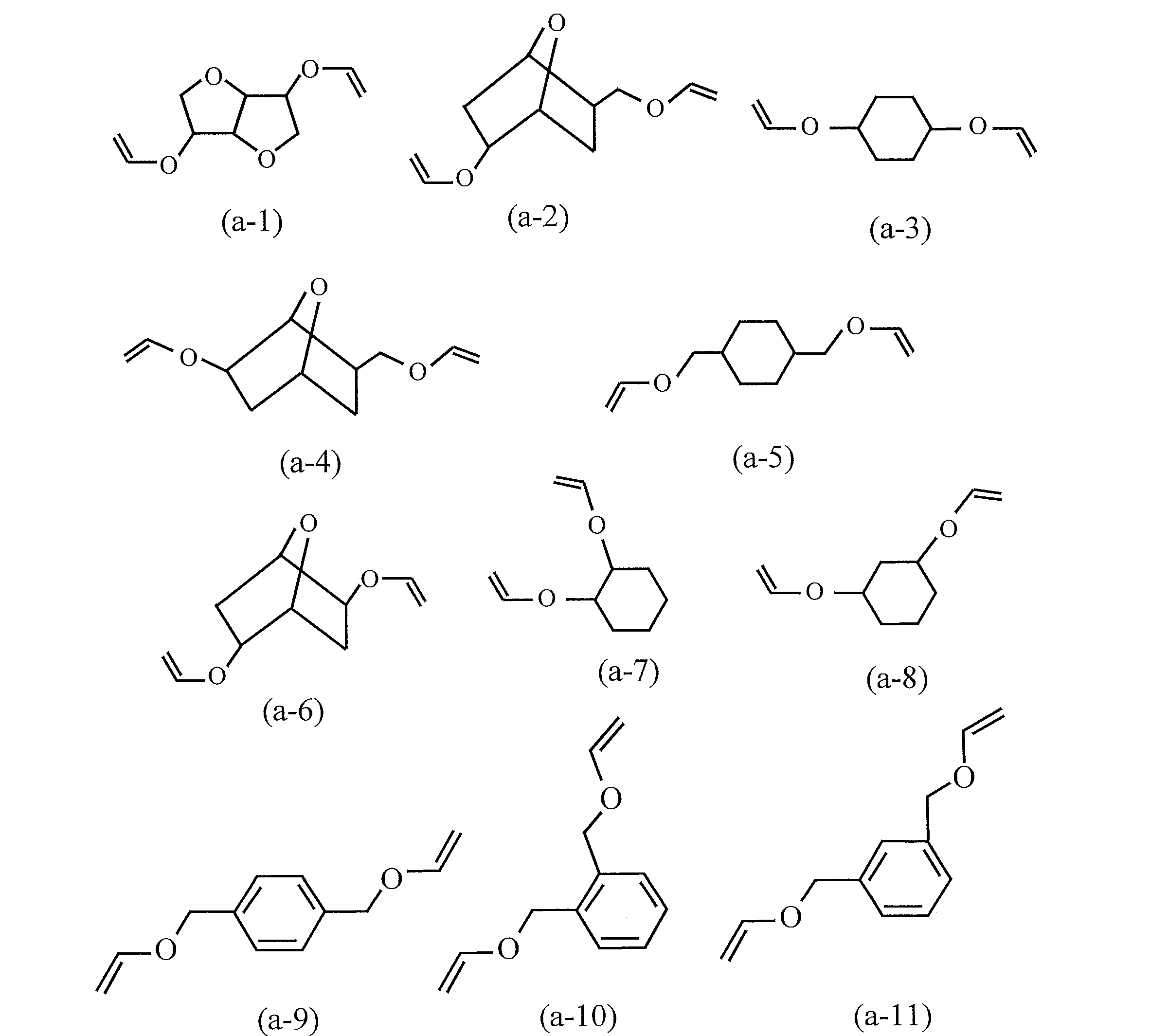
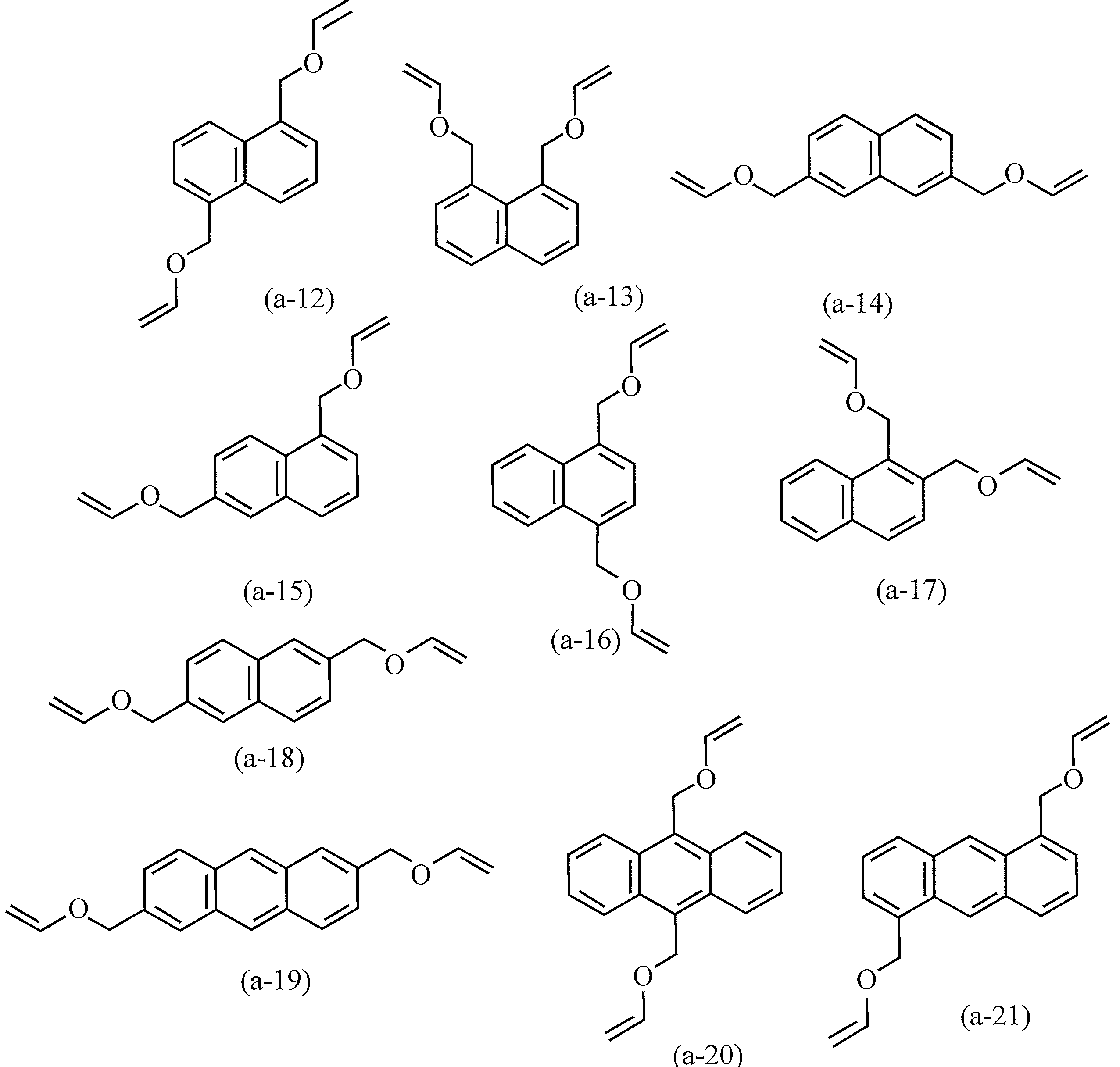
多価ビニルエーテル化合物(A)における上記Z1は、上述の仮接着剤において高軟化点を有する重合体を形成するという観点から、好ましくは、飽和もしくは不飽和脂肪族炭化水素、または複数の当該炭化水素が連結基を介して結合した結合体、の構造式からn1個の水素原子を除去した基であり、より好ましくは、飽和脂肪族炭化水素、または複数の当該炭化水素が連結基を介して結合した結合体、の構造式からn1個の水素原子を除去した基であり、より好ましくは、炭素数1~20の直鎖状アルキレン基、炭素数2~20の分岐鎖状アルキレン基、または、複数の当該アルキレン基が連結基を介して結合した結合体の構造式からn1個の水素原子を除去した基である。
多価ビニルエーテル化合物(A)としては、1,4-ブタンジオールジビニルエーテル、ジエチレングリコールジビニルエーテル、およびトリエチレングリコールジビニルエーテルからなる群より選択される少なくとも一種の化合物が最も好ましい。
仮接着剤中の化合物(B)は、上述のように、多価ビニルエーテル化合物(A)のビニルエーテル基と反応してアセタール結合を形成可能なヒドロキシ基またはカルボキシ基を二つ以上有して多価ビニルエーテル化合物と重合体を形成しうるものであって、例えば、下記の式(b)で表される構成単位(繰り返し単位)を2以上有する化合物である。

式(b)中、Xはヒドロキシ基またはカルボキシ基を表す。n2個のXは、互いに同一であってもよいし、互いに異なってもよい。
式(b)中、n2は1以上の整数を表す。上述の仮接着剤の調製にあたっての入手の容易さや溶剤への溶解のしやすさの観点、および、仮接着剤において高軟化点を有する重合体を形成するという観点から、n2は、好ましくは1~3の整数であり、より好ましくは1~2の整数である。
化合物(B)における上記式(b)で表される構成単位(繰り返し単位)の数は、2以上であり、上述の仮接着剤において高軟化点の重合体を形成するという観点から、好ましくは2~40の整数、より好ましくは10~30の整数である。
式(b)中、Z2は、飽和もしくは不飽和脂肪族炭化水素、飽和もしくは不飽和脂環式炭化水素、芳香族炭化水素、複素環式化合物、またはこれらが単結合もしくは連結基を介して結合した結合体、の構造式から(n2+2)個の水素原子を除去した基を表し、前記飽和もしくは不飽和脂肪族炭化水素、飽和もしくは不飽和脂環式炭化水素、芳香族炭化水素、複素環式化合物、またはこれらが単結合もしくは連結基を介して結合した結合体の構造式としては、上記Z1における例と同様の例を挙げることができる。
化合物(B)は、好ましくは、スチレン系ポリマー、(メタ)アクリル系ポリマー、ポリビニルアルコール、ノボラック樹脂、およびレゾール樹脂であり、より好ましくは、下記式(b-1)~(b-6)からなる群より選択される少なくとも一種の構成単位(繰り返し単位)を2以上有する化合物である。
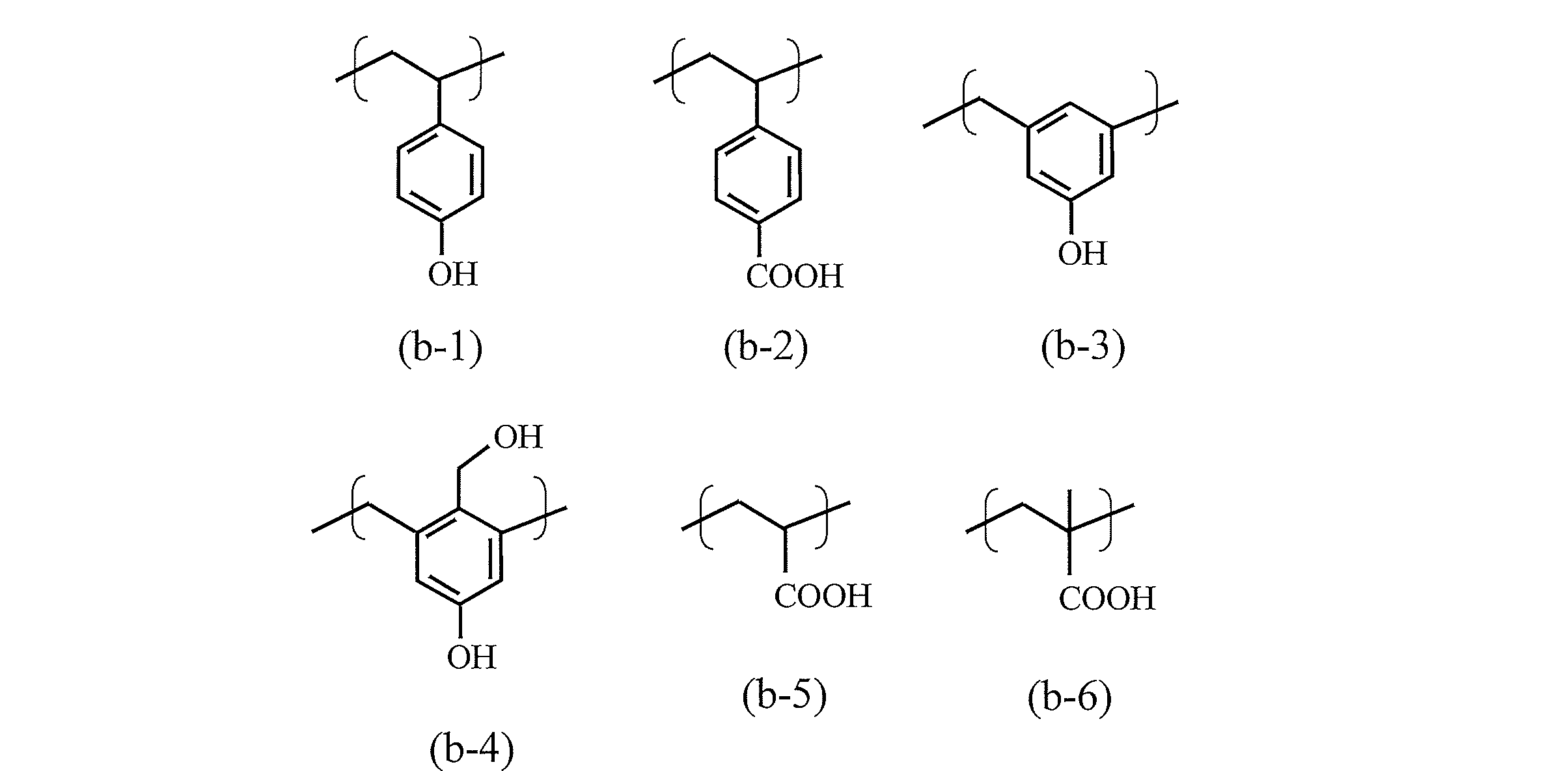
化合物(B)として式(b)中のXがヒドロキシ基である化合物を採用する場合、化合物(B)全量における式(b)で表される構成単位の割合は、好ましくは30質量%以上、より好ましくは50質量%以上、より好ましくは60質量%以上である。また、化合物(B)全量における式(b)で表される構成単位の割合は、好ましくは30モル%以上、より好ましくは50モル%以上である。
化合物(B)として式(b)中のXがカルボキシ基である化合物を採用する場合、化合物(B)全量における式(b)で表される構成単位の割合は、好ましくは1質量%以上、より好ましくは5質量%以上、より好ましくは10質量%以上である。
式(b)で表される構成単位の割合が上記範囲内にあることは、化合物(B)において充分な架橋点間距離や充分な数の架橋点を確保するうえで好適であり、従って、上述の仮接着剤において当該化合物(B)と上述の多価ビニルエーテル化合物(A)との重合によって得られる重合体について重量平均分子量および高軟化点を確保するうえで好適であり、ひいては、当該仮接着剤から形成される仮接着剤層2において高温環境下での高い接着保持性を確保するうえで好適である。
化合物(B)は、式(b)で表される構成単位のみを有する単独重合体であってもよいし、式(b)で表される構成単位と他の構成単位とを有する共重合体であってもよい。化合物(B)が共重合体である場合、ブロック共重合体、グラフト共重合体、およびランダム共重合体のいずれであってもよい。
化合物(B)における上記他の構成単位は、ヒドロキシ基もカルボキシ基も有さない重合性単量体由来の構成単位であり、当該重合性単量体としては、例えば、オレフィン、芳香族ビニル化合物、不飽和カルボン酸エステル、カルボン酸ビニルエステル、および不飽和ジカルボン酸ジエステルが挙げられる。オレフィンとしては、例えば、エチレン、プロピレン、および1-ブテンなど鎖状オレフィン(特にC2-12アルケン)、並びに、シクロペンテン、シクロヘキセン、シクロヘプテン、ノルボルネン、5-メチル-2-ノルボルネン、およびテトラシクロドデセンなど環状オレフィン(特にC3-10シクロアルケン)が挙げられる。芳香族ビニル化合物としえては、例えば、スチレン、ビニルトルエン、α-メチルスチレン、1-プロペニルベンゼン、1-ビニルナフタレン、2-ビニルナフタレン、3-ビニルピリジン、3-ビニルフラン、3-ビニルチオフェン、3-ビニルキノリン、インデン、メチルインデン、エチルインデン、およびジメチルインデンなどC6-14芳香族ビニル化合物が挙げられる。不飽和カルボン酸エステルとしては、例えば、(メタ)アクリル酸エチル、(メタ)アクリル酸ブチル、(メタ)アクリル酸イソブチル、(メタ)アクリル酸2-エチルへキシル、およびジシクロペンタニル(メタ)アクリレートなど不飽和カルボン酸(例えば(メタ)アクリル酸)とアルコール(R”-OH)とを反応させて得られるエステルが挙げられる(前記R”は、飽和もしくは不飽和脂肪族炭化水素、飽和もしくは不飽和脂環式炭化水素、芳香族炭化水素、複素環式化合物、またはこれらが単結合もしくは連結基を介して結合した結合体、の構造式から1個の水素原子を除去した基を表す。R”としては、例えば、上記式(a)中のZ1について挙げた2価の基に対応する1価の基を挙げることができる)。カルボン酸ビニルエステルとしては、例えば、酢酸ビニル、プロピオン酸ビニル、カプリル酸ビニル、およびカプロン酸ビニルなどC1-16脂肪酸ビニルエステルが挙げられる。不飽和ジカルボン酸ジエステルとしては、例えば、マレイン酸ジエチル、マレイン酸ジブチル、マレイン酸ジオクチル、およびマレイン酸2-エチルへキシルなどマレイン酸ジC1-10アルキルエステル、並びに、これらに対応するフマル酸ジエステルを挙げることができる。これらは一種類を単独で、または二種類以上を組み合わせて使用することができる。
共重合体である場合の化合物(B)としては、上記式(b)で表される構成単位と、鎖状オレフィン、環状オレフィン、芳香族ビニル化合物、不飽和カルボン酸エステル、カルボン酸ビニルエステル、および不飽和ジカルボン酸ジエステルからなる群より選択される少なくとも一種の重合性単量体由来の構成単位と、を含む化合物が好ましい。
化合物(B)の軟化点(T1)は、例えば50℃以上であり、好ましくは80℃以上、より好ましくは100℃以上である。このような構成は、当該化合物(B)と上述の多価ビニルエーテル化合物(A)との重合によって得られる重合体について高い軟化点を実現するうえで好適である。また、上述の仮接着剤において適度な流動性を確保して良好な塗布性を実現するという観点からは、T1は、例えば250℃以下、好ましくは200℃以下、より好ましくは150℃以下である。
T1は、例えば、化合物(B)の重量平均分子量(GPC法によるポリスチレン換算値)をコントロールすることによって調整することができる。化合物(B)の重量平均分子量は、例えば1500以上、好ましくは1800~10000、より好ましくは2000~5000である。
仮接着剤中の上述の熱可塑性樹脂(C)としては、熱可塑性を有して、接着剤組成物に配合される場合に接着剤組成物に柔軟性を付与することができる化合物であればよい。そのような熱可塑性樹脂(C)としては、例えば、ポリビニルアセタール系樹脂、ポリエステル系樹脂、ポリウレタン系樹脂、ポリアミド系樹脂、ポリ(チオ)エーテル系樹脂、ポリカーボネート系樹脂、ポリスルホン系樹脂、およびポリイミド系樹脂など重縮合系樹脂、ポリオレフィン系樹脂、(メタ)アクリル系樹脂、スチレン系樹脂、およびビニル系樹脂などビニル重合系樹脂、並びに、セルロース誘導体など天然物由来樹脂を挙げることができる。これらは一種類を単独で、または二種類以上を組み合わせて使用することができる。このような熱可塑性樹脂(C)を上述の仮接着剤が含有するという構成は、形成される仮接着剤層2において、柔軟性や可撓性を付与するうえで好適であり、急激に温度が変化する環境下でも自然剥離やクラックの発生を防止するうえで好適であり、優れた接着性を確保するうえで好適である。
仮接着剤中の熱可塑性樹脂(C)は、好ましくは、ポリビニルアセタール系樹脂、ポリエステル系樹脂、ポリウレタン系樹脂、およびポリアミド系樹脂からなる群より選択される少なくとも一種である。仮接着剤ないし仮接着剤層2において、柔軟性を付与しやすいという観点や、ウエハなど被着体に対する化学的相互作用が減弱して、剥離後の被着体に糊残りが生じる場合であってもその糊残渣を除去しやすいという観点からは、仮接着剤は熱可塑性樹脂(C)としてポリエステル系樹脂を含有するのが好ましい。また、仮接着剤ないし仮接着剤層2において、柔軟性を付与しやすいという観点や、被着体上の糊残渣を除去しやすいという前記観点に加えて、被着体に対する高い密着性を確保するという観点からは、仮接着剤は熱可塑性樹脂(C)としてポリエステル系樹脂とポリビニルアセタール系樹脂とを共に含有するのが好ましい。
前記ポリビニルアセタール系樹脂としては、ポリビニルアルコールにアルデヒド(RCHO)を反応させて得られる、下記式で表される構成単位を少なくとも有する樹脂を挙げることができる。アルデヒド(RCHO)としては、例えば、その構造式中のR(下記式中のRも同じ)が水素原子、直鎖状C1-5アルキル基、分岐鎖状C2-5アルキル基、またはC6-10アリール基である化合物が挙げられ、具体的には、例えばホルムアルデヒド、ブチルアルデヒド、およびベンズアルデヒドが挙げられる。このようなポリビニルアセタール系樹脂は、下記式で表される構成単位以外にも他の構成単位を有していてもよい。すなわち、当該ポリビニルアセタール系樹脂にはホモポリマーおよびコポリマーが含まれる。このようなポリビニルアセタール系樹脂としては、具体的には、ポリビニルホルマールおよびポリビニルブチラールを挙げることができ、例えば、商品名「エスレック KS-1」「エスレック KS-10」(いずれも積水化学工業株式会社製)の市販品を使用することができる。

前記ポリエステル系樹脂としては、例えば、ジオール成分とジカルボン酸成分との重縮合により得られるポリエステルが挙げられる。ジオール成分としては、例えば、エチレングリコールなど脂肪族C2-12ジオール、ジエチレングリコールなどポリオキシC2-4アルキレングリコール、シクロヘキサンジメタノールなど脂環式C5-15ジオール、および、ビスフェノールAなど芳香族C6-20ジオールが挙げられる。ジカルボン酸成分としては、例えば、テレフタル酸など芳香族C8-20ジカルボン酸、アジピン酸など脂肪族C2-40ジカルボン酸、および、シクロヘキサンジカルボン酸など脂環式C8-15ジカルボン酸が挙げられる。前記ポリエステル系樹脂としては、オキシカルボン酸の重縮合により得られるポリエステルも挙げられる。そのオキシカルボン酸としては、例えば、乳酸など脂肪族C2-6オキシカルボン酸、および、ヒドロキシ安息香酸など芳香族C7-19オキシカルボン酸が挙げられる。前記ポリエステル系樹脂としては、ラクトンの開環重合により得られるポリエステルも挙げられる。そのラクトンとしては、例えば、ε-カプロラクトン、δ-バレロラクトン、およびγ-ブチロラクトンなどC4-12ラクトンが挙げられる。前記ポリエステル系樹脂としては、ポリエステルジオールとジイソシアネートとの反応により得られるウレタン結合を含むポリエステルも挙げられる。ポリエステル系樹脂にはホモポリエステルおよびコポリエステルが含まれるものとする。また、ポリエステル系樹脂としては、例えば、商品名「プラクセル H1P」(株式会社ダイセル製)の市販品を使用することができる。
前記ポリウレタン系樹脂としては、例えば、ジイソシアネート類とポリオール類と必要に応じて用いられる鎖伸長剤との反応により得られる樹脂を挙げることができる。ジイソシアネート類としては、ヘキサメチレンジイソシアネートなど脂肪族ジイソシアネート類、イソホロンジイソシアネートなど脂環式ジイソシアネート類、および、トリレンジイソシアネートなど芳香族ジイソシアネート類が挙げられる。ポリオール類としては、ポリエステルジオール、ポリエーテルジオール、およびポリカーボネートジオールが挙げられる。鎖伸長剤としては、エチレングリコールなどC2-10アルキレンジオール、エチレンジアミンなど脂肪族ジアミン類、イソホロンジアミンなど脂環式ジアミン類、および、フェニレンジアミンなど芳香族ジアミン類が挙げられる。
前記ポリアミド系樹脂としては、例えば、ジアミン成分とジカルボン酸成分との重縮合により得られるポリアミド、アミノカルボン酸の重縮合により得られるポリアミド、ラクタムの開環重合により得られるポリアミド、および、ジアミン成分とジカルボン酸成分とジオール成分との重縮合により得られるポリエステルアミドを挙げることができる。前記ジアミン成分としては、例えば、ヘキサメチレンジアミンなどC4-10アルキレンジアミンが挙げられる。前記ジカルボン酸成分としては、例えば、アジピン酸などC4-20アルキレンジカルボン酸が挙げられる。アミノカルボン酸としては、例えば、ω-アミノウンデカン酸などC4-20アミノカルボン酸が挙げられる。前記ラクタムとしては、例えば、ω-ラウロラクタムなどC4-20ラクタムが挙げられる。前記ジオール成分としては、例えば、エチレングリコールなどC2-12アルキレンジオールが挙げられる。また、ポリアミド系樹脂にはホモポリアミドおよびコポリアミドが含まれるものとする。
熱可塑性樹脂(C)の軟化点(T2)は、本発明に係る半導体装置製造方法において熱可塑性樹脂(C)含有の仮接着剤と組み合わせて使用される後述の永久接着剤の熱硬化温度より10℃以上高いことが好ましい。当該永久接着剤の熱硬化温度とT2との差は、例えば10~40℃であり、好ましくは20~30℃である。
T2は、例えば、熱可塑性樹脂(C)の重量平均分子量(Mw:GPC法によるポリスチレン換算値)をコントロールすることによって調整することができる。熱可塑性樹脂(C)の重量平均分子量は、例えば1500~100000であり、好ましくは2000~80000、より好ましくは3000~50000、より好ましくは10000~45000、より好ましくは15000~35000である。
以上のような多価ビニルエーテル化合物(A)、化合物(B)、および熱可塑性樹脂(C)を少なくとも含有する仮接着剤において、多価ビニルエーテル化合物(A)と化合物(B)の重合体の軟化点(T3)は、本発明に係る半導体装置製造方法において当該仮接着剤と組み合わせて使用される後述の永久接着剤の熱硬化温度より10℃以上高いことが好ましい。当該永久接着剤の熱硬化温度とT3との差は、例えば10~40℃であり、好ましくは20~30℃である。
後述の永久接着剤の熱硬化温度が例えば120℃である場合、仮接着剤における多価ビニルエーテル化合物(A)の含有量は、仮接着剤中の化合物(B)におけるヒドロキシ基およびカルボキシ基の総量1モルに対して、多価ビニルエーテル化合物(A)におけるビニルエーテル基が例えば0.01~10モルとなる量であり、好ましくは0.05~5モル、より好ましくは0.07~1モル、より好ましくは0.08~0.5モルとなる量である。
仮接着剤における熱可塑性樹脂(C)の含有量は、仮接着剤中の化合物(B)1質量部に対して例えば0.1~3質量部であり、好ましくは0.2~2質量部、より好ましくは0.3~1質量部である。
仮接着剤における多価ビニルエーテル化合物(A)と化合物(B)と熱可塑性樹脂(C)の合計含有量は、当該仮接着剤の不揮発分全量の例えば70~99.9質量%であり、好ましくは80~99質量%、より好ましくは85~95質量%、より好ましくは85~90質量%である。
仮接着剤は、重合促進剤を更に含有していてもよい。その重合促進剤としては、例えば、下記式(d)で表される1価のカルボン酸、および、下記式(e)で表される1価のアルコールを挙げることができる。これらは一種類を単独で、または二種類以上を組み合わせて使用することができる。仮接着剤が重合促進剤を含有するという構成は、多価ビニルエーテル化合物(A)および化合物(B)の重合反応を促進するうえで好適であり、重合促進剤を含有しない接着剤を使用する場合と比べて、重合時の加熱温度を低下させても、同等の軟化点またはより高い軟化点を有する重合体を形成するうえで好適であり、従って仮接着剤層2において高温環境下(例えば160~180℃程度)での接着性を確保するうえで好適である。
Z3-COOH (d)
(式中、Z3はカルボキシ基以外の置換基を有していてもよい、飽和もしくは不飽和脂肪族炭化水素、飽和もしくは不飽和脂環式炭化水素、および芳香族炭化水素からなる群より選択される一種、の構造式から1個の水素原子を除去した基を表す)
Z4-OH (e)
(式中、Z4はヒドロキシ基以外の置換基を有していてもよい芳香族炭化水素の構造式から1個の水素原子を除去した基を表す)
Z3-COOH (d)
(式中、Z3はカルボキシ基以外の置換基を有していてもよい、飽和もしくは不飽和脂肪族炭化水素、飽和もしくは不飽和脂環式炭化水素、および芳香族炭化水素からなる群より選択される一種、の構造式から1個の水素原子を除去した基を表す)
Z4-OH (e)
(式中、Z4はヒドロキシ基以外の置換基を有していてもよい芳香族炭化水素の構造式から1個の水素原子を除去した基を表す)
上記式(d)中のZ3における飽和もしくは不飽和脂肪族炭化水素、飽和もしくは不飽和脂環式炭化水素、および芳香族炭化水素としては、上記式(a)中のZ1について挙げた飽和もしくは不飽和脂肪族炭化水素、飽和もしくは不飽和脂環式炭化水素、および芳香族炭化水素を挙げることができる。Z3が有していてもよい置換基としては、Z1が有していてもよい置換基の例からカルボキシ基を除いた例を挙げることができる。また、上記式(e)中のZ4における芳香族炭化水素としては、上記式(a)中のZ1について挙げた芳香族炭化水素を挙げることができる。Z4が有していてもよい置換基としては、Z1が有していてもよい置換基の例からヒドロキシ基を除いた例を挙げることができる。
仮接着剤中に重合促進剤が含まれる場合のその重合促進剤のpKa(酸解離定数)は、好ましくは3~8、より好ましくは4~6である。このような構成は、仮接着剤において意図せず重合が進行して粘度が増加すること等を抑制して保存安定性を確保するとともに、当該仮接着剤からの仮接着剤層2の形成にあたって重合促進剤による重合促進効果を確保するうえで、好適である。
式(d)で表される1価のカルボン酸としては、以下に示される化合物(幾何異性体を含む)が好ましい。


式(e)で表される1価のアルコールとしては、以下に示される化合物が好ましい。

仮接着剤中に重合促進剤が含まれる場合のその含有量は、仮接着剤に含まれる多価ビニルエーテル化合物(A)1質量部に対して、例えば0.01~5質量部程度、好ましくは0.1~3質量部、より好ましくは0.3~1質量部である。
仮接着剤は、酸化防止剤を更に含有していてもよい。仮接着剤が酸化防止剤を含有するという構成は、仮接着剤においてその加熱処理時に上述の化合物(B)および熱可塑性樹脂(C)の酸化を防止するうえで好適である。仮接着剤中の化合物(B)および熱可塑性樹脂(C)の酸化防止は、当該仮接着剤から形成される仮接着剤層2について加熱処理を施して得られる軟化組成物の溶剤に対する溶解性を確保するうえで好適であり、従って、ウエハなど被着体から仮接着剤層2が加熱処理を経て剥離された後に当該被着体に糊残りが生じる場合であってもその糊残渣を除去するうえで好適である。
酸化防止剤としては、例えば、フェノール系酸化防止剤、リン系酸化防止剤、チオエステル系酸化防止剤、およびアミン系酸化防止剤を挙げることができる。これらは一種を単独で、または二種以上を組み合わせて使用することができる。フェノール系酸化防止剤は、加熱処理時における酸化防止効果が特に優れるので、仮接着剤中の酸化防止剤として好ましい。
フェノール系酸化防止剤としては、例えば、ペンタエリスリトールテトラキス[3(3,5-ジ-t-ブチル-4-ヒドロキシフェニル)プロピオネート]、チオジエチレンビス[3-(3,5-ジ-t-ブチル-4-ヒドロキシフェニル)プロピオネート]、3-(3,5-ジ-t-ブチル-4-ヒドロキシフェニル)プロピオン酸オクタデシル、N,N'-ヘキサメチレンビス[3-(3,5-ジ-t-ブチル-4-ヒドロキシフェニル)プロピオンアミド]、3-(4-ヒドロキシ-3,5-ジイソプロピルフェニル)プロピオン酸オクチル、1,3,5-トリス(4-ヒドロキシ-3,5-ジ-t-ブチルベンジル)-2,4,6-トリメチルベンゼン、2,4-ビス(ドデシルチオメチル)-6-メチルフェノール、および、カルシウムビス[3,5-ジ(t-ブチル)-4-ヒドロキシベンジル(エトキシ)ホスフィナート]を挙げることができる。フェノール系酸化防止剤としては、例えば、商品名「Irganox 1010」「Irganox 1035」「Irganox 1076」「Irganox 1098」「Irganox 1135」「Irganox 1330」「Irganox 1726」「Irganox 1425WL」(いずれもBASF社製)の市販品を使用することができる。
仮接着剤中に酸化防止剤が含まれる場合のその含有量は、仮接着剤に含まれる化合物(B)と熱可塑性樹脂(C)との合計100質量部に対して、例えば0.01~15質量部であり、好ましくは0.1~12質量部、より好ましくは0.5~10質量部である。
仮接着剤は、必要に応じて他の成分を更に含有していてもよい。他の成分としては、例えば、酸発生剤、界面活性剤、溶剤、レベリング剤、シランカップリング剤、および発泡剤を挙げることができる。これらは一種を単独で、または二種以上を組み合わせて使用することができる。
仮接着剤中に界面活性剤が含まれる場合、当該仮接着剤における界面活性剤の含有量は、好ましくは0.01~1質量%程度である。このような構成は、仮接着剤塗布時のハジキを抑制するうえで好適であり、塗膜の均一性を確保するうえで好適である。そのような界面活性剤としては、例えば、商品名「F-444」「F-447」「F-554」「F-556」「F-557」(いずれもDIC社製のフッ素系オリゴマー)、商品名「BYK-350」(ビックケミー社製のアクリル系ポリマー)、および、商品名「A-1420」「A-1620」「A-1630」(いずれもダイキン工業株式会社製のフッ素含有アルコール)が挙げられる。これらは一種を単独で、または二種以上を組み合わせて使用することができる。
仮接着剤は、その粘度調整の観点から溶剤を含有するのが好ましい。溶剤としては、例えば、トルエン、ヘキサン、イソプロパノール、メチルイソブチルケトン、シクロペンタノン、シクロヘキサノン、プロピレングリコールモノメチルエーテルアセテート、プロピレングリコールモノメチルエーテル、およびγ-ブチロラクトンが挙げられる。これらは一種を単独で、または二種以上を組み合わせて使用することができる。仮接着剤が溶剤を含有する場合、仮接着剤の溶剤含有量は例えば55~80質量%である。
仮接着剤は、その構成成分を、必要に応じて真空下で気泡を除去しながら、撹拌・混合することによって調製することができる。撹拌・混合時の当該混合物の温度は10~80℃程度が好ましい。撹拌・混合には、例えば、自転公転型ミキサー、1軸または多軸エクストルーダー、プラネタリーミキサー、ニーダー、またはディゾルバーを使用することができる。
仮接着剤の粘度(25℃およびせん断速度50/sの条件で測定される粘度)は、例えば30~2000mPa・s程度であり、好ましくは300~1500mPa・s、より好ましくは500~1500mPa・sである。このような構成は、仮接着剤について、その塗布性を確保してウエハなど被着体の表面に均一に塗布するうえで好適である。
以上のような仮接着剤を、ウエハなど被着体の表面に塗布した後、加熱処理を施すことにより、当該仮接着剤中の多価ビニルエーテル化合物(A)のビニルエーテル基と化合物(B)のヒドロキシ基および/またはカルボキシ基とをアセタール結合させて、多価ビニルエーテル化合物(A)および化合物(B)から重合体を生じさせることができる。例えば、多価ビニルエーテル化合物(A)として下記式(a')で表される化合物を含有し、且つ下記式(b')で表される構成単位を有する化合物を化合物(B)として含有する仮接着剤に加熱処理を施して、これら両化合物を重合させると、下記式(P)で表される重合体が得られる。

仮接着剤を加熱処理に付すことにより得られる重合体の軟化点(T3)は、多価ビニルエーテル化合物(A)と化合物(B)との相対的な量を調整することによってコントロールすることができ、当該仮接着剤と組み合わせて使用される後述の永久接着剤の熱硬化温度が120℃である場合、重合体の軟化点(T3)は、例えば130℃以上であり、好ましくは130~170℃、より好ましくは140~160℃である。
多価ビニルエーテル化合物(A)と化合物(B)との上記重合体、多価ビニルエーテル化合物(A)、化合物(B)、および熱可塑性樹脂(C)の各軟化点は、下記フロー条件下で高化式フローテスターを使用して測定することができる。
<フロー条件>
圧力:100kg/cm2
スピード:6℃/分
ノズル:1mmφ×10mm
<フロー条件>
圧力:100kg/cm2
スピード:6℃/分
ノズル:1mmφ×10mm
また、仮接着剤から形成される仮接着剤層の軟化点については、次のようにして求められる温度とする。まず、仮接着剤0.1gを第1のガラス板に10μmの厚さで塗布して仮接着剤の塗膜を形成する。次に、その塗膜上に第2のガラス板を重ね合わせる。次に、加熱処理を経ることにより、第1および第2のガラス板の間の仮接着剤内で多価ビニルエーテル化合物(A)および化合物(B)を重合させて当該仮接着剤を硬化させ、当該仮接着剤を介して両ガラス板を接合する。加熱処理は、例えば、140℃での2分間の加熱、それに続く200℃での2分間の加熱、それに続く230℃での4分間の加熱を含む。このような接着剤接合により、第1のガラス板と、第2のガラス板と、その間の仮接着剤層との積層構造を有する積層体が得られる。この積層体について、第2のガラス板を固定した状態で、加熱しつつ第1のガラス板を水平方向(ガラス板の面内方向)に2kgの応力を掛けて引っ張り、第1のガラス板が動き始める時の温度を測定する。以上のようにして求められる温度を軟化点とする。
本半導体装置製造方法においては、次に、図1(b)に示すように、補強ウエハ1Rにおいてそのウエハ1を薄化する(薄化工程)。具体的には、支持基板Sに支持された状態にあるウエハ1に対してその裏面1b側からグラインド装置を使用して研削加工を行うことによって、ウエハ1を所定の厚さに至るまで薄化して薄化ウエハ1Tを形成する。薄化後のウエハ1(薄化ウエハ1T)の厚さは、例えば1~20μmである。
次に、例えば図3に示すように、補強ウエハ1Rの薄化ウエハ1T側を、ベースウエハであるウエハ3に対して接着剤4を介して接合する(接合工程)。
ウエハ3は、半導体素子が作り込まれ得る半導体ウエハ本体を有するベースウエハであり、素子形成面3aおよびこれとは反対の裏面3bを有する。ウエハ3の半導体ウエハ本体をなすための構成材料としては、例えば、ウエハ1の半導体ウエハ本体をなすための構成材料として上掲したものを採用することができる。ベースウエハであるウエハ3の厚さは、製造プロセス中の当該ウエハ3を含むウエハ積層体の強度を確保するという観点からは、好ましくは300μm以上、より好ましくは500μm以上、より好ましくは700μm以上である。ウエハ3に対する後述の研削工程における研削時間の短縮化の観点からは、ウエハ3の厚さは、好ましくは1000μm以下、より好ましくは900μm以下、より好ましくは800μm以下である。
接着剤4は、ウエハ間の接合状態を実現するための熱硬化型接着剤であり、好ましくは、熱硬化性樹脂としての重合性基含有ポリオルガノシルセスキオキサン(即ち、重合性官能基を有するポリオルガノシルセスキオキサン)を含有する。重合性基含有ポリオルガノシルセスキオキサンの有する重合性官能基は、好ましくは、エポキシ基または(メタ)アクリロイルオキシ基である。重合性基含有ポリオルガノシルセスキオキサンは、形成される接着剤層において高い耐熱性を実現するとともに、接着剤層形成のための硬化温度の低下を図って被着体たるウエハ内の素子へのダメージを抑制するのに適する。接着剤4における重合性基含有ポリオルガノシルセスキオキサンの含有割合は、例えば70質量%以上であり、好ましくは80~99.8質量%、より好ましくは90~99.5質量%である。接着剤4中の熱硬化性樹脂としては、重合性基含有ポリオルガノシルセスキオキサンに代えてベンゾシクロブテン(BCB)樹脂またはノボラック系エポキシ樹脂を採用してもよい。
接着剤4に含有される重合性基含有ポリオルガノシルセスキオキサンは、本実施形態では、シロキサン構成単位として、下記の式(1)で表される構成単位を少なくとも含む第1構成単位[RSiO3/2]、および、下記の式(2)で表される構成単位を少なくとも含む第2構成単位[RSiO2/2(OR')]を含む(第2構成単位におけるRとR'は同じであってもよいし異なってもよい)。これら構成単位はシロキサン構成単位におけるいわゆるT単位に属し、本実施形態では、構成単位[RSiO3/2]をT3体とし、構成単位[RSiO2/2(OR')]をT2体とする。T3体において、そのケイ素原子は、それぞれが他のシロキサン構成単位中のケイ素原子とも結合する三つの酸素原子と結合している。T2体において、そのケイ素原子は、それぞれが他のシロキサン構成単位中のケイ素原子とも結合する二つの酸素原子と結合し、且つアルコキシ基の酸素と結合している。このようなT3体およびT2体は、いずれも、上述のようにシロキサン構成単位としてのT単位に属し、加水分解性の三つの官能基を有するシラン化合物の加水分解とその後の縮合反応によって形成されうる、重合性基含有ポリオルガノシルセスキオキサンの部分構造である。

式(1)におけるR1および式(2)におけるR1は、それぞれ、エポキシ基または(メタ)アクリロイルオキシ基を含有する基を表す。式(2)におけるR2は、水素原子、または、炭素数1~4のアルキル基を表す。
式(1)および式(2)における各R1がエポキシ基含有基である場合のそのR1としては、例えば、下記の式(3)~(6)で表される基が挙げられる。式(3)~(6)におけるR3,R4,R5,R6のそれぞれは、炭素数が例えば1~10の直鎖状または分岐鎖状のアルキレン基を表す。そのようなアルキレン基としては、例えば、メチレン基、メチルメチレン基、ジメチルメチレン基、エチレン基、プロピレン基、トリメチレン基、テトラメチレン基、ペンタメチレン基、ヘキサメチレン基、およびデカメチレン基が挙げられる。接着剤4から形成される接着剤層における高い耐熱性の実現や硬化時収縮の抑制の観点からは、式(1)および式(2)におけるエポキシ基含有基としてのR1は、それぞれ、好ましくは、式(3)で表されるエポキシ基含有基または式(4)で表されるエポキシ基含有基であり、より好ましくは、式(3)で表される基であってR3がエチレン基である2-(3,4-エポキシシクロヘキシル)エチル基である。

上記式(2)におけるR2は、上述のように、水素原子または炭素数1~4のアルキル基を表し、従って、式(2)におけるOR2は、ヒドロキシ基、または、炭素数1~4のアルコキシ基を表す。炭素数1~4のアルコキシ基としては、例えば、メトキシ基、エトキシ基、プロポキシ基、イソプロポキシ基、ブトキシ基、およびイソブチルオキシ基が挙げられる。
接着剤4に含まれる重合性基含有ポリオルガノシルセスキオキサンは、上記式(1)で表される構成単位として、一種類を含むものでもよいし、二種類以上を含むものでもよい。当該重合性基含有ポリオルガノシルセスキオキサンは、上記式(2)で表される構成単位として、一種類を含むものでもよいし、二種類以上を含むものでもよい。
接着剤4に含まれる上述の重合性基含有ポリオルガノシルセスキオキサンは、上記のT3体として、式(1)で表される構成単位に加えて、下記の式(7)で表される構成単位を含んでもよい。式(7)におけるR7は、水素原子、置換もしくは無置換のアルキル基、置換もしくは無置換のアルケニル基、置換もしくは無置換のシクロアルキル基、置換もしくは無置換のアリール基、または、置換もしくは無置換のアラルキル基を表す。式(7)におけるR7は、好ましくは、置換もしくは無置換のアルキル基、置換もしくは無置換のアルケニル基、または置換もしくは無置換のアリール基であり、より好ましくはフェニル基である。

R7に関して上記したアルキル基としては、例えば、メチル基、エチル基、プロピル基、n-ブチル基、イソプロピル基、イソブチル基、s-ブチル基、t-ブチル基、およびイソペンチル基が挙げられる。R7に関して上記したアルケニル基としては、例えば、ビニル基、アリル基、およびイソプロペニル基が挙げられる。R7に関して上記したシクロアルキル基としては、例えば、シクロブチル基、シクロペンチル基、およびシクロヘキシル基が挙げられる。R7に関して上記したアリール基としては、例えば、フェニル基、トリル基、およびナフチル基が挙げられる。R7に関して上記したアラルキル基としては、例えば、ベンジル基およびフェネチル基が挙げられる。
R7に関して上記したアルキル基、アルケニル基、シクロアルキル基、アリール基、およびアラルキル基の置換基としては、例えば、エーテル基、エステル基、カルボニル基、シロキサン基、フッ素原子などハロゲン原子、アクリル基、メタクリル基、メルカプト基、アミノ基、および水酸基が挙げられる。
接着剤4に含まれる上述の重合性基含有ポリオルガノシルセスキオキサンは、上記のT2体として、式(2)で表される構成単位に加えて、下記の式(8)で表される構成単位を含んでもよい。式(8)におけるR7は、水素原子、置換もしくは無置換のアルキル基、置換もしくは無置換のアルケニル基、置換もしくは無置換のシクロアルキル基、置換もしくは無置換のアリール基、または、置換もしくは無置換のアラルキル基を表し、具体的には上記式(7)におけるR7と同様である。式(8)におけるR2は、水素原子または炭素数1~4のアルキル基を表し、具体的には上記式(2)におけるR2と同様である。

接着剤4に含まれる上述の重合性基含有ポリオルガノシルセスキオキサンは、そのシロキサン構成単位中に、T単位である上述の第1および第2構成単位に加えて、いわゆるM単位である構成単位[R3SiO1/2]、いわゆるD単位である構成単位[R2SiO2/2]、およびいわゆるQ単位である構成単位[SiO4/2]からなる群より選択される少なくとも一種を含んでもよい。
重合性基含有ポリオルガノシルセスキオキサンは、カゴ型、不完全カゴ型、ラダー型、ランダム型のいずれのシルセスキオキサン構造を有していてもよく、これらシルセスキオキサン構造の2以上が組み合わせられた構造を有していてもよい。
接着剤4中の重合性基含有ポリオルガノシルセスキオキサンの全シロキサン構成単位において、T2体に対するT3体のモル比の値(即ち、T3体/T2体)は、例えば5~500であり、下限値は、好ましくは10である。上限値は、好ましくは100、より好ましくは50である。重合性基含有ポリオルガノシルセスキオキサンについては、[T3体/T2体]の値の当該範囲への調整により、接着剤4に含まれる重合性基含有ポリオルガノシルセスキオキサン以外の成分との相溶性が向上し、取扱い性が向上する。重合性基含有ポリオルガノシルセスキオキサンにおける[T3体/T2体]の値が5~500であることは、T3体に対してT2体の存在量が相対的に少なく、シラノールの加水分解・縮合反応がより進行していることを意味する。
重合性基含有ポリオルガノシルセスキオキサンにおける上記モル比の値(T3体/T2体)は、例えば、29Si-NMRスペクトル測定により求めることができる。29Si-NMRスペクトルにおいて、上述の第1構成単位(T3体)におけるケイ素原子と、上述の第2構成単位(T2体)におけるケイ素原子とは、異なるケミカルシフトのピークないしシグナルを示す。これらピークの面積比から、上記モル比の値を求めることができる。重合性基含有ポリオルガノシルセスキオキサンの29Si-NMRスペクトルは、例えば、下記の装置および条件により測定することができる。
測定装置:商品名「JNM-ECA500NMR」(日本電子株式会社製)
溶媒:重クロロホルム
積算回数:1800回
測定温度:25℃
溶媒:重クロロホルム
積算回数:1800回
測定温度:25℃
接着剤4に含まれる重合性基含有ポリオルガノシルセスキオキサンの数平均分子量(Mn)は、好ましくは1000~50000であり、より好ましくは1500~10000、より好ましくは2000~8000、より好ましくは2000~7000である。数平均分子量を1000以上とすることにより、形成される硬化物ないし接着剤層の絶縁性や、耐熱性、耐クラック性、接着性が向上する。一方、数平均分子量を50000以下とすることにより、接着剤4中の重合性基含有ポリオルガノシルセスキオキサンと他成分との相溶性が向上し、形成される硬化物ないし接着剤層の絶縁性や、耐熱性、耐クラック性が向上する。
接着剤4に含まれる重合性基含有ポリオルガノシルセスキオキサンについての分子量分散度(Mw/Mn)は、好ましくは1.0~4.0であり、より好ましくは1.1~3.0、より好ましくは1.2~2.7である。分子量分散度を4.0以下とすることにより、形成される硬化物ないし接着剤層の耐熱性や、耐クラック性、接着性がより高くなる。一方、分子量分散度を1.0以上とすることにより、当該接着剤組成物が液状となりやすく、その取り扱い性が向上する傾向がある。
重合性基含有ポリオルガノシルセスキオキサンの数平均分子量(Mn)および重量平均分子量(Mw)は、ゲル・パーミエーション・クロマトグラフィー(GPC)により測定してポリスチレン換算により算出される値とする。重合性基含有ポリオルガノシルセスキオキサンの数平均分子量(Mn)および重量平均分子量(Mw)は、例えば、HPLC装置(商品名「LC-20AD」,株式会社島津製作所製)を使用して下記の条件により測定することができる。
カラム:2本のShodex KF-801(上流側,昭和電工株式会社製)と、Shodex KF-802(昭和電工株式会社製)と、Shodex KF-803(下流側,昭和電工株式会社製)とを直列に接続
測定温度:40℃
溶離液:テトラヒドロフラン(THF)
試料濃度:0.1~0.2質量%
流量:1mL/分
標準試料:ポリスチレン
検出器:UV-VIS検出器(商品名「SPD-20A」,株式会社島津製作所製)
測定温度:40℃
溶離液:テトラヒドロフラン(THF)
試料濃度:0.1~0.2質量%
流量:1mL/分
標準試料:ポリスチレン
検出器:UV-VIS検出器(商品名「SPD-20A」,株式会社島津製作所製)
以上のような重合性基含有ポリオルガノシルセスキオキサンは、加水分解性の三つの官能基を有するシラン化合物の加水分解とこれに続く縮合反応によって製造することができる。その製造に用いられる原料は、下記の式(9)で表される化合物を少なくとも含み、下記の式(10)で表される化合物を必要に応じて含む。式(9)で表される化合物は、上記式(1)で表される構成単位と上記式(2)で表される構成単位を形成するためのものである。式(10)で表される化合物は、上記式(7)で表される構成単位と上記式(8)で表される構成単位を形成するためのものである。

式(9)におけるR1は、重合性基を含有する基を表し、具体的には上記式(1)(2)におけるR1と同様である。式(9)におけるX1は、アルコキシ基またはハロゲン原子を表す。そのアルコキシ基としては、例えば、メトキシ基、エトキシ基、プロポキシ基、イソプロピルオキシ基、ブトキシ基、イソブチルオキシ基など炭素数1~4のアルコキシ基が挙げられる。X1としてのハロゲン原子としては、例えば、フッ素原子、塩素原子、臭素原子、およびヨウ素原子が挙げられる。X1は、好ましくはアルコキシ基であり、より好ましくはメトキシ基またはエトキシ基である。式(9)において、三つのX1は互いに同じであってもよいし異なってもよい。
式(10)におけるR7は、置換もしくは無置換のアリール基、置換もしくは無置換のアラルキル基、置換もしくは無置換のシクロアルキル基、置換もしくは無置換のアルキル基、または、置換もしくは無置換のアルケニル基を表し、具体的には上記式(7)(8)におけるR7と同様である。式(10)におけるX2は、アルコキシ基またはハロゲン原子を表し、具体的には上記式(9)におけるX1と同様である。
上述の重合性基含有ポリオルガノシルセスキオキサンの製造に用いられる原料は、更に他の加水分解性シラン化合物を含んでもよい。そのような化合物としては、例えば、上記式(9)(10)で表される両化合物以外の加水分解性三官能シラン化合物、M単位を形成することとなる加水分解性単官能シラン化合物、D単位を形成することとなる加水分解性二官能シラン化合物、および、Q単位を形成する加水分解性四官能シラン化合物が挙げられる。
上記原料としての加水分解性シラン化合物の使用量や組成は、製造目的物である重合性基含有ポリオルガノシルセスキオキサンの構造に応じて適宜に調整される。例えば、上記式(9)で表される化合物の使用量は、使用する加水分解性シラン化合物全量に対して、例えば55~100モル%、好ましくは65~100モル%である。上記式(10)で表される化合物の使用量は、使用する加水分解性シラン化合物全量に対して、例えば0~70モル%である。使用する加水分解性シラン化合物全量に対する、式(9)で表される化合物と式(10)で表される化合物との総使用量は、例えば60~100モル%、好ましくは70~100モル%、より好ましくは80~100モル%である。
上述の重合性基含有ポリオルガノシルセスキオキサンの製造において二種類以上の加水分解性シラン化合物を用いる場合、加水分解性シラン化合物の種類ごとの加水分解および縮合反応は、同時に行うこともできるし、順次に行うこともできる。
上述の加水分解および縮合反応は、好ましくは、一種類のまたは二種類以上の溶媒の存在下で行われる。好ましい溶媒としては、例えば、ジエチルエーテル、ジメトキシエタン、テトラヒドロフラン、ジオキサンなどのエーテル、および、アセトンや、メチルエチルケトン、メチルイソブチルケトンなどのケトンが挙げられる。溶媒の使用量は、加水分解性シラン化合物100質量部あたり、例えば2000質量部以下の範囲内で反応時間等に応じて適宜に調整される。
上述の加水分解および縮合反応は、好ましくは、一種類のまたは二種類以上の触媒および水の存在下で進行される。触媒は、酸触媒であってもよいし、アルカリ触媒であってもよい。触媒の使用量は、加水分解性シラン化合物1モルあたり例えば0.002~0.2モルの範囲内で適宜に調整される。水の使用量は、加水分解性シラン化合物1モルあたり例えば0.5~20モルの範囲内で適宜に調整される。
上記加水分解性シラン化合物の加水分解および縮合反応は、1段階で行ってもよいし、2段階以上に分けて行ってもよい。上記モル比の値(T3体/T2体)が5以上である重合性基含有ポリオルガノシルセスキオキサンを製造する場合には例えば、第1段目の加水分解および縮合反応の反応温度は、例えば40~100℃、好ましくは45~80℃である。第1段目の加水分解および縮合反応の反応時間は、例えば0.1~10時間、好ましくは1.5~8時間である。第2段目の加水分解および縮合反応の反応温度は、好ましくは5~200℃、より好ましくは30~100℃である。反応温度を上記範囲に制御することにより、上記モル比の値(T3体/T2体)および上記数平均分子量をより効率的に所望の範囲に制御できる傾向がある。また、第2段目の加水分解および縮合反応の反応時間は、特に限定されないが、0.5~1000時間が好ましく、より好ましくは1~500時間である。また、上述の加水分解および縮合反応は、常圧下、加圧下、または減圧下で行うことができる。上述の加水分解および縮合反応は、好ましくは、窒素やアルゴンなど不活性ガスの雰囲気下で行われる。
以上のような加水分解性シラン化合物の加水分解および縮合反応により、上述の重合性基含有ポリオルガノシルセスキオキサンが得られる。反応終了後には、好ましくは、重合性基の開環を抑制するための触媒の中和を行う。こうして得られた重合性基含有ポリオルガノシルセスキオキサンは、必要に応じて精製される。
接着剤4は、例えば以上のようにして製造される重合性基含有ポリオルガノシルセスキオキサンに加えて、好ましくは少なくとも一種類の硬化触媒を含む。
接着剤4がエポキシ基含有ポリオルガノシルセスキオキサンを含む場合の硬化触媒としては、例えば熱カチオン重合開始剤が挙げられる。接着剤4が(メタ)アクリロイルオキシ基含有ポリオルガノシルセスキオキサンを含む場合の硬化触媒としては、例えば熱ラジカル重合開始剤が挙げられる。接着剤4における硬化触媒の含有量は、重合性基含有ポリオルガノシルセスキオキサン100質量部あたり、好ましくは0.1~3.0質量部である。
上述の熱カチオン重合開始剤としては、例えば、アリールスルホニウム塩、アルミニウムキレート、三フッ化ホウ素アミン錯体などのタイプの熱カチオン重合開始剤が挙げられる。アリールスルホニウム塩としては、例えばヘキサフルオロアンチモネート塩が挙げられる。アルミニウムキレートとしては、例えば、エチルアセトアセテートアルミニウムジイソプロピレート、およびアルミニウムトリス(エチルアセトアセテート)が挙げられる。三フッ化ホウ素アミン錯体としては、例えば、三フッ化ホウ素モノエチルアミン錯体、三フッ化ホウ素イミダゾール錯体、および三フッ化ホウ素ピペリジン錯体が挙げられる。
上述の熱ラジカル重合開始剤としては、例えば、アゾ化合物や過酸化物などのタイプの熱ラジカル重合開始剤が挙げられる。アゾ化合物としては、例えば、2,2'-アゾビスイソブチロニトリル、2,2'-アゾビス(2,4-ジメチルバレロニトリル)、2,2'-アゾビス(4-メトキシ-2,4-ジメチルバレロニトリル)、ジメチル-2,2'-アゾビス(2-メチルプロピオネート)、2,2'-アゾビス(イソ酪酸)ジメチル、ジエチル-2,2'-アゾビス(2-メチルプロピオネート)、およびジブチル-2,2'-アゾビス(2-メチルプロピオネート)が挙げられる。過酸化物としては、例えば、ベンゾイルパーオキサイド、t-ブチルパーオキシ-2-エチルヘキサノエート、2,5-ジメチル-2,5-ジ(2-エチルヘキサノイル)パーオキシヘキサン、t-ブチルパーオキシベンゾエート、t-ブチルパーオキサイド、クメンハイドロパーオキサイド、ジクミルパーオキサイド、ジ-t-ブチルパーオキサイド、2,5-ジメチル-2,5-ジブチルパーオキシヘキサン、2,4-ジクロロベンゾイルパーオキサイド、1,4-ジ(2-t-ブチルパーオキシイソプロピル)ベンゼン、1,1-ビス(t-ブチルパーオキシ)-3,3,5-トリメチルシクロヘキサン、メチルエチルケトンパーオキサイド、および1,1,3,3-テトラメチルブチルパーオキシ-2-エチルヘキサノエートが挙げられる。
接着剤4は、上述の重合性基含有ポリオルガノシルセスキオキサンに加えて、一種類のまたは二種類以上の他の硬化性化合物を含んでもよい。当該硬化性化合物としては、例えば、上述の重合性基含有ポリオルガノシルセスキオキサン以外のエポキシ化合物、(メタ)アクリロイルオキシ基含有化合物、ビニル基含有化合物、オキセタン化合物、およびビニルエーテル化合物が挙げられる。
上述の重合性基含有ポリオルガノシルセスキオキサン以外のエポキシ化合物としては、例えば、脂環式エポキシ化合物(脂環式エポキシ樹脂)、芳香族エポキシ化合物(芳香族エポキシ樹脂)、および脂肪族エポキシ化合物(脂肪族エポキシ樹脂)が挙げられる。脂環式エポキシ化合物としては、例えば、3,4,3',4'-ジエポキシビシクロヘキサン、2,2-ビス(3,4-エポキシシクロヘキシル)プロパン、1,2-ビス(3,4-エポキシシクロヘキシル)エタン、2,3-ビス(3,4-エポキシシクロヘキシル)オキシラン、ビス(3,4-エポキシシクロヘキシルメチル)エーテル、および、2,2-ビス(ヒドロキシメチル)-1-ブタノールの1,2-エポキシ-4-(2-オキシラニル)シクロヘキサン付加物(例えば、株式会社ダイセル製の「EHPE3150」)が挙げられる。
上記芳香族エポキシ化合物としては、例えば、エピビスタイプグリシジルエーテル型エポキシ樹脂やノボラック・アルキルタイプグリシジルエーテル型エポキシ樹脂が挙げられる。
上記脂肪族エポキシ化合物としては、例えば、環状構造を有しないq価のアルコール(qは自然数である)のグリシジルエーテル、一価カルボン酸または多価カルボン酸のグリシジルエステル、および、二重結合を有する油脂のエポキシ化物が挙げられる。二重結合を有する油脂のエポキシ化物としては、例えば、エポキシ化亜麻仁油、エポキシ化大豆油、およびエポキシ化ひまし油が挙げられる。
上述の(メタ)アクリロイルオキシ基含有化合物としては、例えば、トリメチロールプロパントリ(メタ)アクリレート、ジトリメチロールプロパンテトラ(メタ)アクリレート、ペンタエリスリトールトリ(メタ)アクリレート、ペンタエリスリトールテトラ(メタ)アクリレート、ジペンタエリスリトールペンタ(メタ)アクリレート、ジペンタエリスリトールヘキサ(メタ)アクリレート、グリセリントリ(メタ)アクリレート、トリス(2-ヒドロキシエチル)イソシアヌレートトリ(メタ)アクリレート、エチレングリコールジ(メタ)アクリレート、1,3-ブタンジオールジ(メタ)アクリレート、1,4-ブタンジオールジ(メタ)アクリレート、1,6-ヘキサンジオールジ(メタ)アクリレート、ネオペンチルグリコールジ(メタ)アクリレート、ジエチレングリコールジ(メタ)アクリレート、トリエチレングリコールジ(メタ)アクリレート、ジプロピレングリコールジ(メタ)アクリレート、ビス(2-ヒドロキシエチル)イソシアヌレートジ(メタ)アクリレート、ジシクロペンタニルジアクリレート、エポキシアクリレート、ウレタンアクリレート、不飽和ポリエステル、ポリエステルアクリレート、ポリエーテルアクリレート、ビニルアクリレート、シリコーンアクリレート、およびポリスチリルエチルメタクリレートが挙げられる。また、上述の(メタ)アクリロイルオキシ基含有化合物としては、ナガセケムテックス株式会社製の「DA-141」、東亞合成株式会社製の「アロニックスM-211B」および「アロニックスM-208」、並びに、新中村化学株式会社製の「NKエステル」「ABE-300」「A-BPE-4」「A-BPE-10」「A-BP E-20」「A-BPE-30」「BPE-100」「BPE-200」「BPE-500」「BPE-900」「BPE-1300N」も挙げられる。
上述のビニル基含有化合物としては、例えば、スチレンおよびジビニルベンゼンが挙げられる。
上述のオキセタン化合物としては、例えば、3,3-ビス(ビニルオキシメチル)オキセタン、3-エチル-3-(ヒドロキシメチル)オキセタン、3-エチル-3-(2-エチルヘキシルオキシメチル)オキセタン、3-エチル-3-(ヒドロキシメチル)オキセタン、3-エチル-3-[(フェノキシ)メチル]オキセタン、3-エチル-3-(ヘキシルオキシメチル)オキセタン、3-エチル-3-(クロロメチル)オキセタン、および3,3-ビス(クロロメチル)オキセタンが挙げられる。
上述のビニルエーテル化合物としては、例えば、2-ヒドロキシエチルビニルエーテル、3-ヒドロキシプロピルビニルエーテル、2-ヒドロキシプロピルビニルエーテル、2-ヒドロキシイソプロピルビニルエーテル、4-ヒドロキシブチルビニルエーテル、3-ヒドロキシブチルビニルエーテル、2-ヒドロキシブチルビニルエーテル、3-ヒドロキシイソブチルビニルエーテル、2-ヒドロキシイソブチルビニルエーテル、1-メチル-3-ヒドロキシプロピルビニルエーテル、1-メチル-2-ヒドロキシプロピルビニルエーテル、1-ヒドロキシメチルプロピルビニルエーテル、4-ヒドロキシシクロヘキシルビニルエーテル、1,6-ヘキサンジオールモノビニルエーテル、1,6-ヘキサンジオールジビニルエーテル、1,8-オクタンジオールジビニルエーテル、p-キシレングリコールモノビニルエーテル、p-キシレングリコールジビニルエーテル、m-キシレングリコールモノビニルエーテル、m-キシレングリコールジビニルエーテル、o-キシレングリコールモノビニルエーテル、o-キシレングリコールジビニルエーテル、ジエチレングリコールモノビニルエーテル、ジエチレングリコールジビニルエーテル、トリエチレングリコールモノビニルエーテル、およびトリエチレングリコールジビニルエーテルが挙げられる。
接着剤4は、その塗工性等を調整するうえでは溶剤を含むのが好ましい。溶剤としては、例えば、プロピレングリコールモノメチルエーテルアセテート、メチルエチルケトン、メチルイソブチルケトン、シクロヘキサノン、トルエン、キシレン、酢酸エチル、酢酸ブチル、3-メトキシブチルアセテート、メトキシプロピルアセテート、エチレングリコールモノメチルエーテルアセテート、メタノール、エタノール、イソプロピルアルコール、1-ブタノール、1-メトキシ-2-プロパノール、3-メトキシブタノール、エトキシエタノール、ジイソプロピルエーテル、エチレングリコールジメチルエーテル、およびテトラヒドロフランが挙げられる。
接着剤4は、更に、シランカップリング剤、消泡剤、酸化防止剤、ブロッキング防止剤、レベリング剤、界面活性剤、増量剤、防錆剤、帯電防止剤、可塑剤など、各種の添加剤を含んでもよい。
接着剤4の耐熱性に関し、接着剤4の熱分解温度は、好ましくは200℃以上、より好ましくは260℃以上、より好ましくは300℃以上である。熱分解温度は、示差熱熱重量同時測定装置を使用して行う熱重量分析によって得られる曲線、即ち、分析対象である試料についての所定昇温範囲での熱重量の温度依存性を表す曲線における、昇温過程初期の重量減少のない或いは一定割合でわずかに漸減している部分の接線と、昇温過程初期に続く昇温過程中期の有意な重量減少が生じている部分内にある変曲点での接線との交点が示す温度とする。示差熱熱重量同時測定装置としては、例えば、セイコーインスツル株式会社製の商品名「TG-DTA6300」を使用することができる。
本半導体装置製造方法における接合工程では、以上のような接着剤4を介して、ウエハ3の素子形成面3a側と、補強ウエハ1Rにおける薄化ウエハ1Tの裏面1b側とを、接合する。
具体的には、まず、接合対象面(ウエハ3の素子形成面3a,薄化ウエハ1Tの裏面1b)の一方または両方に接着剤4をスピンコーティングによって塗布して接着剤層を形成する。図3(a)は、ウエハ3の素子形成面3aに接着剤4が塗布される場合を例示的に示すものである。また、接着剤4の塗布の前に、接合対象面の一方または両方にシランカップリング剤処理を施してもよい。次に、加熱によって接着剤4(接着剤層)を乾燥させて固化させる。このときの加熱温度は例えば50~150℃であり、加熱時間は例えば5~120分間である。加熱温度は、一定であってもよいし、段階的に変化させてもよい。次に、接着剤4(接着剤層)を介して接合対象面を貼り合わせる。この貼り合わせにおいて、加圧力は例えば300~5000g/cm2であり、温度は、例えば30~200℃であり、好ましくは室温以上かつ80℃以下の範囲である。その後、接合対象面間において加熱によって接着剤4を硬化させる。硬化のための加熱温度は、例えば30~200℃であり、好ましくは50~190℃である。硬化のための加熱時間は例えば5~120分間である。加熱温度は、一定であってもよいし、段階的に変化させてもよい。接着剤4の硬化後における接着剤層の厚さは、例えば0.5~20μmである。本工程において比較的低温で接着剤4を硬化させて接着剤接合を実現するという以上の構成は、貼合わせ時にウエハ間に介在する接着剤4の寸法変化を抑制するのに適するとともに、被着体たるウエハ内の素子へのダメージを抑制するのにも適する。
本半導体装置製造方法では、次に、図4(a)および図4(b)に示すように、補強ウエハ1Rにおける支持基板Sと薄化ウエハ1Tの間の仮接着剤層2による仮接着状態を解除して、支持基板Sの取り外しを行う(取外し工程)。取外し工程は、好ましくは、仮接着剤層2中の上述の重合体、即ち、多価ビニルエーテル化合物(A)と化合物(B)との重合体、の軟化点(T3)より高い温度で仮接着剤層2を軟化させる軟化処理を含む。この軟化処理における仮接着剤層加熱温度は、好ましくは170℃以上であり、且つ、例えば250℃以下であり、好ましくは240℃以下、より好ましくは230℃以下である。本工程では、例えばこのような軟化処理の後、ウエハ1に対して支持基板Sをスライドさせて、支持基板Sの分離ないし取外しを行う。補強ウエハ1Rの取外しの後、ウエハ1上に仮接着剤が残っている場合には、当該仮接着剤を除去する。この除去作業には、仮接着剤が易溶解性を示す一種類または二種類以上の溶剤を使用することができる。そのような溶剤としては、例えば、シクロヘキサノン、プロピレングリコールモノメチルエーテル、プロピレングリコールモノメチルエーテルアセテート、アセトン、酢酸エチル、酢酸ブチル、およびメチルイソブチルケトンが挙げられる。上述の補強ウエハ1Rにおけるウエハ1がその素子形成面1a側に絶縁膜や配線パターンを含む配線構造を伴わないものである場合、本工程の後、薄化ウエハ1Tの素子形成面1a上に配線構造が形成される。後記の取外し工程の後においても同様である。
本実施形態の半導体装置製造方法では、上述の補強ウエハ1Rとは別に、所定数の補強ウエハ1R(図1(a)に示される)が追加的に用意される。補強ウエハ1Rは、上述のように、素子形成面1aおよび裏面1bを有するウエハ1と、支持基板Sと、これらの間の仮接着剤層2とを含む積層構造を有する。仮接着剤層2は、上述の仮接着剤から形成されるものである。そして、各補強ウエハ1Rにおいて、図1(b)に示すようにウエハ1を薄化する。具体的には、各補強ウエハ1Rにおいて、支持基板Sに支持された状態にあるウエハ1に対してその裏面1b側からグラインド装置を使用して研削加工を行うことによって、ウエハ1を所定の厚さに至るまで薄化して薄化ウエハ1Tを形成する。薄化後のウエハ1(薄化ウエハ1T)の厚さは、例えば1~20μmである。
次に、図5(a)および図5(b)に示すように、ベースウエハであるウエハ3上に積層された薄化ウエハ1Tの素子形成面1a側と、追加の補強ウエハ1Rにおける薄化ウエハ1Tの裏面1b側とを、上述の接着剤4を介して接合する(追加の接合工程)。
具体的には、まず、接合対象面(一方の薄化ウエハ1Tの素子形成面1a,他方の薄化ウエハ1Tの裏面1b)の一方または両方に接着剤4をスピンコーティングによって塗布して接着剤層を形成する。図5(a)は、一方の薄化ウエハ1Tの素子形成面1aに接着剤4が塗布される場合を例示的に示すものである。また、接着剤4の塗布の前に、接合対象面の一方または両方にシランカップリング剤処理を施してもよい。次に、加熱によって接着剤4(接着剤層)を乾燥させて固化させる。このときの加熱温度は例えば50~150℃であり、加熱時間は例えば5~120分間である。加熱温度は、一定であってもよいし、段階的に変化させてもよい。次に、接着剤4(接着剤層)を介して接合対象面を貼り合わせる。この貼り合わせにおいて、加圧力は例えば300~5000g/cm2であり、温度は、例えば30~200℃であり、好ましくは室温以上かつ80℃以下の範囲である。その後、接合対象面間において加熱によって接着剤4を硬化させる。硬化のための加熱温度は、例えば30~200℃であって好ましくは50~190℃であり、硬化のための加熱時間は例えば5~120分間である。加熱温度は、一定であってもよいし、段階的に変化させてもよい。接着剤4の硬化後における接着剤層の厚さは、例えば0.5~20μmである。本工程において比較的低温で接着剤4を硬化させて接着剤接合を実現するという以上の構成は、貼合わせ時にウエハ間に介在する接着剤4の寸法変化を抑制するのに適するとともに、被着体たるウエハ内の素子へのダメージを抑制するのにも適する。
本半導体装置製造方法では、次に、図6(a)および図6(b)に示すように、更に積層された補強ウエハ1Rにおける支持基板Sと薄化ウエハ1Tの間の仮接着剤層2による仮接着状態を解除して、支持基板Sの取り外しを行う(追加の接合工程後の取外し工程)。本工程は、好ましくは、仮接着剤層2中の上述の重合体、即ち、多価ビニルエーテル化合物(A)と化合物(B)との重合体、の軟化点(T3)より高い温度で仮接着剤層2を軟化させる軟化処理を含む。この軟化処理における仮接着剤層加熱温度は、好ましくは170℃以上であり、且つ、例えば250℃以下であり、好ましくは240℃以下、より好ましくは230℃以下である。本工程では、例えばこのような軟化処理の後、ウエハ1に対して支持基板Sをスライドさせて、支持基板Sの分離ないし取外しを行う。補強ウエハ1Rの取外しの後、ウエハ1上に仮接着剤が残っている場合には、当該仮接着剤を除去する。
本半導体装置製造方法では、用意される追加の補強ウエハ1Rごとに、補強ウエハ1Rのウエハ1を薄化する薄化工程(図1)、上述の追加の接合工程(図5)、およびその後の取外し工程(図6)を含む一連の過程を繰り返すことにより、複数の薄化ウエハ1Tを順次に積層してウエハ積層体Yを形成ることができる(ウエハ積層体形成工程)。ウエハ積層体形成工程では、少なくとも二つのウエハ積層体Yを形成する。ウエハ積層体Y間において、ウエハ積層数は同じであってもよいし異なってもよい。図7には、ウエハ3上に3枚の薄化ウエハ1Tが多段に配された構成を有するウエハ積層体Yを一例として表す。
次に、図8に示すように、各ウエハ積層体Yにおいて貫通電極5を形成する(電極形成工程)。貫通電極5は、ウエハ積層体Yにおいて異なるウエハに形成されている半導体素子間を電気的に接続するためのものであり、ウエハ積層体Yにおける積層方向の一端に位置する薄化ウエハ1T(第1のウエハ)の素子形成面1aから他端に位置するウエハ3(第2のウエハ)の素子形成面3aを超える位置まで当該ウエハ積層体Y内を貫通して延びる。本工程では、例えば、全ての薄化ウエハ1Tと接着剤4(接着剤層)とを貫通し且つ上は3内に入り込む開口部の形成、当該開口部の内壁面への絶縁膜(図示略)の形成、絶縁膜表面へのバリア層(図示略)の形成、バリア層表面への電気めっき用シード層(図示略)の形成、および、電気めっき法による開口部内への銅など導電材料の充填を経るなどして、貫通電極5を形成することができる。開口部の形成手法としては例えば反応性イオンエッチングが挙げられる。また、貫通電極5の形成には、例えば特開2016-4835号公報に記載の手法を採用してもよい。形成される貫通電極5により、具体的には、各薄化ウエハ1Tの素子形成面1aの側に形成されている配線構造(図示略)およびウエハ3の素子形成面3aの側に形成されている配線構造(図示略)が、相互に電気的に接続される。このような貫通電極5によると、製造される半導体装置において、半導体素子間を短距離で適切に電気的接続できる。したがって、このような貫通電極5を形成するという構成は、製造される半導体装置において、効率の良いデジタル信号処理を実現するうえで好適であり、高周波信号の減衰を抑制するうえで好適であり、また、消費電力を抑制するうえでも好適である。
本半導体装置製造方法においては、次に、図9に示すように、各ウエハ積層体Yにおけるウエハ3の裏面3b側に対する研削によって当該ウエハ3を薄化して、その裏面3b側にて貫通電極5を露出させる(電極端部露出化工程)。薄化後のウエハ3の厚さは、例えば5~200μmである。本工程を経たウエハ積層体Yでは、貫通電極5は、ウエハ積層方向の一端に位置する薄化ウエハ1T(第1のウエハ)の素子形成面1aにて露出するとともに、ウエハ積層方向の他端に位置するウエハ3(第2のウエハ)の裏面3bにて露出することとなる。
本半導体装置製造方法においては、次に、電極端部露出化工程を経た二つのウエハ積層体Yを、それらウエハ積層体Y間にて貫通電極5を電気的に接続しつつ、積層して接合する(多層化工程)。
多層化工程では、図10に示すように、接合対象である一方のウエハ積層体Yにおける薄化ウエハ1T(第1のウエハ)の素子形成面1a側と、他方のウエハ積層体Yにおける薄化ウエハ1T(第1のウエハ)の素子形成面1a側との接合が、行われてもよい(ウエハ積層体間のface-to-face接合)。接合手法としては、一方のウエハ積層体Yの貫通電極5と他方のウエハ積層体Yの貫通電極5との間にバンプを介在させるバンプ接合や、いわゆる直接接合が挙げられ、直接接合としては、例えば、Cu電極間のCu-Cu接合など電極間ダイレクト接合が挙げられる(後記のウエハ積層体間接合における接合手法についても同様である)。図10は、直接接合によってウエハ積層体Yどうしがface-to-face接合される場合を一例として表すものである。
多層化工程では、図11に示すように、接合対象である一方のウエハ積層体Yにおける薄化ウエハ1T(第1のウエハ)の素子形成面1a側と、他方のウエハ積層体Yにおけるウエハ3(第2のウエハ)の裏面3b側との接合が、行われてもよい(ウエハ積層体間のface-to-back接合)。接合手法としては、上述のバンプ接合や直接接合が挙げられる。図11は、直接接合によってウエハ積層体Yどうしがface-to-back接合される場合を一例として表すものである。
多層化工程では、図12に示すように、接合対象である一方のウエハ積層体Yにおけるウエハ3(第2のウエハ)の裏面3b側と、他方のウエハ積層体Yにおけるウエハ3(第2のウエハ)の裏面3b側との接合が、行われてもよい(ウエハ積層体間のback-to-back接合)。接合手法としては、上述のバンプ接合や直接接合が挙げられる。図12は、直接接合によってウエハ積層体Yどうしがback-to-back接合される場合を一例として表すものである。
この後、得られるウエハ積層体の積層方向の両端に位置するウエハの表面に絶縁膜(図示略)を形成し、当該ウエハ積層体内の配線構造(図示略)と電気的に接続する外部接続用バンプ(図示略)を一方の絶縁膜上に形成してもよい。
以上のようにして、半導体素子がその厚さ方向に集積された立体的構造を有する半導体装置を製造することができる。この半導体装置は、ダイシングによって個片化されてもよい。
本実施形態の半導体装置製造方法における上述の電極形成工程では、各ウエハ積層体Y内に、それに含まれる複数のウエハにわたって延びる貫通電極5が形成される。このような構成は、ウエハ積層体Yの形成過程でウエハごとに貫通電極を形成するための一連のステップ(即ち、一枚のウエハを貫通する開口部の形成や、その開口部の内壁面への絶縁膜の形成、開口部内への導電材料の充填、これらに伴う各種態様の洗浄処理など)の実施を回避または削減するのに適し、WOWプロセスにおいて半導体装置を効率よく製造するのに適する。
本実施形態の半導体装置製造方法における上述の多層化工程では、既に貫通電極5が形成されている二つのウエハ積層体Y,Yの間で貫通電極5が電気的に接続されつつウエハ積層体Y,Yが接合されて、ウエハが更に多層化される。このような構成は、WOWプロセスにおいて大きなウエハ積層数を実現するのに適する。
WOWプロセスにおいては、ウエハ積層体のウエハ積層数が増加するほど、積層体厚さ方向において当該複数のウエハにわたって延びる開口部を適切に形成するのが困難となる傾向にあって当該開口部内に貫通電極を適切に形成することが困難となる傾向にある。しかしながら、本半導体装置製造方法では、製造目的の半導体装置の半導体素子積層数に相当する積層数のウエハ積層体Yを一括的に貫通する電極を形成する必要はない。このような本半導体装置製造方法は、一括貫通電極の形成に伴う上述の困難性を回避または抑制するのに適する。
以上のように、本実施形態の半導体装置製造方法は、ウエハ積層体の増大に伴う貫通電極の形成の困難性を回避または抑制して大きなウエハ積層数を実現しつつ、効率よく半導体装置を製造するのに適するのである。
また、本半導体装置製造方法は、上記の電極形成工程における貫通電極形成手法として例えば特開2016-4835号公報に記載の手法を採用する場合に、各ウエハにおける半導体素子の高密度化を図るのに適する。同文献に記載の貫通電極形成手法によると、例えば図13に示すように、連なって貫通電極Eをなすこととなる、各ウエハW内に形成される部分導電部Eaが、隣接ウエハW間では異なる断面積(ウエハ面内方向の断面積)で形成され、ウエハ積層数が増すほど部分導電部Eaの断面積がウエハWごとに不可避的に漸増する構造が生ずる。このような構造においては、ウエハ積層数が増すほど、ウエハWにおける半導体素子形成可能面積は小さくなって素子の高密度化を図りにくくなる。しかしながら、上述の本半導体装置製造方法では、製造目的の半導体装置の半導体素子積層数に相当する積層数のウエハ積層体を一括的に貫通する電極を形成する必要はない。このような本半導体装置製造方法は、ウエハ積層数の増大を図りつつ各ウエハにおける半導体素子の高密度化を図るのに、適するのである。
本半導体装置製造方法において、補強ウエハ1R内の仮接着剤層2を形成するための仮接着剤は、上述のように、好ましくは、多価ビニルエーテル化合物(A)と、そのビニルエーテル基と反応してアセタール結合を形成可能なヒドロキシ基またはカルボキシ基を二つ以上有して多価ビニルエーテル化合物と重合体を形成しうる化合物(B)と、熱可塑性樹脂(C)とを含有する。このような構成の仮接着剤は、支持基板Sとウエハ1の間に硬化形成される仮接着剤層の形態において、図1(b)を参照して上述した薄化工程でのウエハ1に対する研削等に耐えうる高い接着力を確保しつつ、例えば130~250℃程度の比較的に高い軟化温度を実現するのに適する。
本半導体装置製造方法において、図3を参照して上述した接合工程で使用される接着剤4は、上述のように、好ましくは重合性基含有ポリオルガノシルセスキオキサンを含有する。上述のように、重合性基含有ポリオルガノシルセスキオキサンは、例えば30~200℃程度の比較的に低い重合温度ないし硬化温度を実現するのに適するとともに、硬化後において高い耐熱性を実現するのに適し、従って、重合性基含有ポリオルガノシルセスキオキサン含有接着剤によるウエハ間接着剤接合は、ウエハ間に形成される接着剤層において高い耐熱性を実現するとともに、接着剤層形成のための硬化温度の低下を図って被着体たるウエハ内の素子へのダメージを抑制するのに適する。
仮接着剤層2形成用の仮接着剤とウエハ間接合用の接着剤4とにつき共に上述の好ましい構成が採用される場合、次のような複合的で機能的な構成を実現することができる。図3を参照して上述した接合工程に供される補強ウエハ1R内の仮接着剤層2が上述のように比較的高い軟化温度を実現するのに適し、且つ、同工程で使用される接着剤4(重合性基含有ポリオルガノシルセスキオキサン含有接着剤)が上述のように比較的低い硬化温度と硬化後の高耐熱性とを実現するのに適するという、構成である。このような複合的な機能的構成は、接合工程の実施と図4を参照して上述したその後の取外し工程の実施とを両立させるのに適する。すなわち、当該構成は、接合工程を比較的低温の条件で実施して、補強ウエハ1Rにおける支持基板Sと薄化ウエハ1Tの仮接着状態を維持しつつベースウエハたるウエハ3に対する当該薄化ウエハ1Tの良好な接着剤接合を実現するのに適するとともに、その後の取外し工程を比較的高温の条件で実施して、ウエハ3と薄化ウエハ1Tの間の接着剤接合を維持しつつ仮接着剤層2を軟化させて薄化ウエハ1Tからの支持基板Sの取り外しを実施するのに適する。薄化ウエハ1Tからの支持基板Sの取り外しにあたって仮接着剤層2の軟化を経て仮接着剤層2による仮接着状態を解除するという構成は、薄化ウエハ1Tに対して局所的に強い応力が作用するのを回避または抑制して当該ウエハの破損を回避するのに適する。上記の複合的構成は、ウエハ積層体Yの形成にあたり、ウエハ破損を回避しつつ接着剤接合を介して薄いウエハを多層化するのに適するのである。
本半導体装置製造方法においては、図1から図6を参照して上述したウエハ積層体形成工程に代えて図14および図15に示すウエハ積層体形成工程を経て、ウエハ積層体Yを形成してもよい。
このウエハ積層体形成工程では、まず、図14(a)および図14(b)に示すように、後に半導体素子が作り込まれることとなる半導体ウエハであるウエハ1'と、既に半導体素子が作り込まれている素子形成面3aを片面に有するウエハ3とが、上述した接着剤4を介して接合される。具体的には、まず、接合対象面(ウエハ3の素子形成面3a,ウエハ1'の一方の面)の一方または両方に接着剤4をスピンコーティングによって塗布して接着剤層を形成する。接着剤4の塗布の前に、接合対象面の一方または両方にシランカップリング剤処理を施してもよい。次に、加熱によって接着剤4(接着剤層)を乾燥させて固化させる。次に、接着剤4(接着剤層)を介して接合対象面を貼り合わせる。その後、接合対象面間において加熱によって接着剤4を硬化させる。接着剤4の硬化後における接着剤層の厚さは、例えば0.5~20μmである。接着剤4による接合をなすための諸条件については、図3を参照して上述した接合工程における諸条件と同様である。
次に、図14(c)に示すように、ウエハ1'が薄化される。本工程では、例えば、ウエハ1'に対する研削加工によってウエハ1'を所定の厚さにまで薄化して薄化ウエハ1T'を形成する。薄化後のウエハ1'(薄化ウエハ1T')の厚さは、例えば1~20μmである。
次に、図14(d)に示すように、薄化ウエハ1T'の被研削面側に素子形成面1aを形成する。具体的には、薄化ウエハ1T'の被研削面側に対し、トランジスタ形成工程や配線形成工程などを経て複数の半導体素子(図示略)を作り込む。これにより、被研削面側に素子形成面1aを有する薄化ウエハ1Tが形成される。
次に、図15(a)および図15(b)に示すように、後に半導体素子が作り込まれることとなる半導体ウエハである新たなウエハ1'と薄化ウエハ1Tとが、上述した接着剤4を介して接合される。具体的には、まず、接合対象面(薄化ウエハ1Tの素子形成面1a,新たなウエハ1'の一方の面)の一方または両方に接着剤4をスピンコーティングによって塗布して接着剤層を形成する。接着剤4の塗布の前に、接合対象面の一方または両方にシランカップリング剤処理を施してもよい。次に、加熱によって接着剤4(接着剤層)を乾燥させて固化させる。次に、接着剤4(接着剤層)を介して接合対象面を貼り合わせる。その後、接合対象面間において加熱によって接着剤4を硬化させる。接着剤4の硬化後における接着剤層の厚さは、例えば0.5~20μmである。接着剤4による接合をなすための諸条件については、図3を参照して上述した接合工程における諸条件と同様である。
次に、図15(c)に示すように、ウエハ1'が薄化される。本工程では、例えば、ウエハ1'に対する研削加工によってウエハ1'を所定の厚さにまで薄化して薄化ウエハ1T'を形成する。薄化後のウエハ1'(薄化ウエハ1T')の厚さは、例えば1~20μmである。
次に、図15(d)に示すように、薄化ウエハ1T'の被研削面側に素子形成面1aを形成する。具体的には、薄化ウエハ1T'の被研削面側に対し、トランジスタ形成工程や配線形成工程などを経て複数の半導体素子(図示略)を作り込む。これにより、被研削面側に素子形成面1aを有する薄化ウエハ1Tが形成される。
上述の半導体装置製造方法では、下段ウエハに対するウエハ1'の接合と、そのウエハ1'の薄化と、薄化後のウエハ1'に対する半導体素子の形成とを含む一連の過程を以上のように所定の回数繰り返すウエハ積層体形成工程を、採用してもよい。
以上のまとめとして本発明の構成及びそのバリエーションを以下に付記する。
[1] 素子形成面およびこれとは反対の裏面をそれぞれが有する複数のウエハを、隣り合う二つのウエハにおいて一方のウエハの素子形成面と他方のウエハの裏面とが向かい合う配向で含む、積層構造をそれぞれが有する、少なくとも二つのウエハ積層体を形成するウエハ積層体形成工程と、
前記ウエハ積層体における積層方向の一端に位置し且つ裏面側に隣接ウエハが位置する第1のウエハの素子形成面側から、他端に位置する第2のウエハの素子形成面を超える位置まで、当該ウエハ積層体内を貫通して延びる貫通電極を、各ウエハ積層体に形成する電極形成工程と、
前記電極形成工程を経た各ウエハ積層体における前記第2のウエハの裏面側に対する研削によって当該第2のウエハを薄化して当該裏面側にて前記貫通電極を露出させる、電極端部露出化工程と、
前記電極端部露出化工程を経た少なくとも二つのウエハ積層体を、当該ウエハ積層体間にて貫通電極を電気的に接続しつつ、積層して接合する多層化工程と、を含む半導体装置製造方法。
[2] 前記電極形成工程は、前記ウエハ積層体において前記第1のウエハの素子形成面側から前記第2のウエハの素子形成面を超える位置まで延びる開口部を形成する工程と、当該開口部内に導電材料を充填する工程とを含む、[1]に記載の半導体装置製造方法。
[3] 前記電極端部露出化工程において、薄化後の第2のウエハの厚さが、5~200μmである、[1]または[2]に記載の半導体装置製造方法。
[4] 前記多層化工程では、接合対象である一方のウエハ積層体における第1のウエハの素子形成面側と、他方のウエハ積層体における第1のウエハの素子形成面側との接合が、行われる、[1]~[3]のいずれか一つに記載の半導体装置製造方法。
[5] 前記多層化工程では、接合対象である一方のウエハ積層体における第1のウエハの素子形成面側と、他方のウエハ積層体における第2のウエハの裏面側との接合が、行われる、[1]~[3]のいずれか一つに記載の半導体装置製造方法。
[6] 前記多層化工程では、接合対象である一方のウエハ積層体における第2のウエハの裏面側と、他方のウエハ積層体における第2のウエハの裏面側との接合が、行われる、[1]~[3]のいずれか一つに記載の半導体装置製造方法。
[7] 前記ウエハ積層体形成工程は、素子形成面およびこれとは反対の裏面を有するベースウエハの前記素子形成面側にウエハを接合する工程と、当該ウエハに対する研削によって前記ベースウエハ上に薄化ウエハを形成する工程と、当該薄化ウエハにおける被研削面側に半導体素子を形成する工程とを含む、[1]~[6]のいずれか一つに記載の半導体装置製造方法。
[8] 前記ウエハ積層体形成工程は、前記ベースウエハ上の前記薄化ウエハの素子形成面側にウエハを接合する工程と、当該ウエハに対する研削によって前記ベースウエハ上に薄化ウエハを形成する工程と、当該薄化ウエハにおける被研削面側に半導体素子を形成する工程とを更に含む、[7]に記載の半導体装置製造方法。
[9] 前記薄化ウエハの厚さが、1~20μmである、[7]または[8]に記載の半導体装置製造方法。
[10] 前記ウエハ積層体形成工程は、
素子形成面およびこれとは反対の裏面を有するウエハ、支持基板、並びに、前記ウエハの前記素子形成面側および前記支持基板の間の仮接着剤層、を含む積層構造を有する補強ウエハを用意する工程と、
前記補強ウエハにおける前記ウエハをその裏面側から研削して薄化ウエハを形成する工程と、
素子形成面およびこれとは反対の裏面を有するベースウエハの前記素子形成面側と、前記補強ウエハの前記薄化ウエハの裏面側とを、接着剤を介して接合する接合工程と、
前記補強ウエハにおける前記支持基板と前記薄化ウエハの間の前記仮接着剤層による仮接着状態を解除して前記支持基板の取り外しを行う取外し工程と、を含む、[1]~[6]のいずれか一つに記載の半導体装置製造方法。
[11] 前記ウエハ積層体形成工程は、
素子形成面およびこれとは反対の裏面を有するウエハ、支持基板、並びに、前記ウエハの前記素子形成面側および前記支持基板の間の仮接着剤層、を含む積層構造を有する少なくとも一つの追加の補強ウエハを用意する工程と、
各追加の補強ウエハにおける前記ウエハをその裏面側から研削して薄化ウエハを形成する工程と、
前記追加の補強ウエハにおける前記薄化ウエハの裏面側を、前記ベースウエハ上の薄化ウエハの素子形成面側に前記接着剤を介して接合する、少なくとも一つの追加の接合工程と、
前記追加の接合工程ごとに行われる少なくとも一つの、前記追加の補強ウエハにおける前記支持基板と前記薄化ウエハの間の前記仮接着剤層による仮接着状態を解除して前記支持基板の取り外しを行う取外し工程と、を更に含む、[10]に記載の半導体装置製造方法。
[12] 前記ウエハの構成材料が、シリコン(Si)、ゲルマニウム(Ge)、炭化ケイ素(SiC)、ガリウムヒ素(GaAs)、窒化ガリウム(GaN)、またはインジウムリン(InP)である、[1]~[11]のいずれか一つに記載の半導体装置製造方法。
[13] 前記ウエハの厚さが、1000μm以下である、[1]~[12]のいずれか一つに記載の半導体装置製造方法。
[14] 前記支持基板が、シリコンウエハまたはガラスウエハである、[10]~[13]のいずれか一つに記載の半導体装置製造方法。
[15] 前記支持基板が、シリコンウエハである、[14]に記載の半導体装置製造方法。
[16] 前記支持基板の厚さが、300μm以上800μm以下である、[10]~[15]のいずれか一つに記載の半導体装置製造方法。
[17] 前記支持基板の厚さが、700μm以上800μm以下である、[10]~[16]のいずれか一つに記載の半導体装置製造方法。
[18] 前記仮接着剤層を形成するための仮接着剤は、多価ビニルエーテル化合物と、そのビニルエーテル基と反応してアセタール結合を形成可能なヒドロキシ基またはカルボキシ基を二つ以上有して前記多価ビニルエーテル化合物と重合体を形成しうる化合物と、熱可塑性樹脂とを含有する、[10]~[17]のいずれか一つに記載の半導体装置製造方法。
[19] 前記接着剤は、重合性基含有ポリオルガノシルセスキオキサンを含有する、[10]~[18]のいずれか一つに記載の半導体装置製造方法。
[20] 前記多価ビニルエーテル化合物が、上記式(a)で表される分子内に二つ以上のビニルエーテル基を有する化合物である、[10]~[19]のいずれか一つに記載の半導体装置製造方法。
[21] 前記多価ビニルエーテル化合物が、1,4-ブタンジオールジビニルエーテル、ジエチレングリコールジビニルエーテル、およびトリエチレングリコールジビニルエーテル、並びに、上記式(a-1)~(a-21)で表される化合物からなる群より選択される少なくとも一種の化合物である、[10]~[19]のいずれか一つに記載の半導体装置製造方法。
[22] 前記多価ビニルエーテル化合物が、1,4-ブタンジオールジビニルエーテル、ジエチレングリコールジビニルエーテル、およびトリエチレングリコールジビニルエーテルからなる群より選択される少なくとも一種の化合物である、[10]~[19]のいずれか一つに記載の半導体装置製造方法。
[23] 前記多価ビニルエーテル化合物が、1,4-ブタンジオールジビニルエーテル、およびトリエチレングリコールジビニルエーテルからなる群より選択される少なくとも一種の化合物である、[10]~[19]のいずれか一つに記載の半導体装置製造方法。
[24] 前記多価ビニルエーテル化合物が、ジエチレングリコールジビニルエーテル、およびトリエチレングリコールジビニルエーテルからなる群より選択される少なくとも一種の化合物である、[10]~[19]のいずれか一つに記載の半導体装置製造方法。
[25] 前記多価ビニルエーテル化合物が、1,4-ブタンジオールジビニルエーテル、およびジエチレングリコールジビニルエーテルからなる群より選択される少なくとも一種の化合物である、[10]~[19]のいずれか一つに記載の半導体装置製造方法。
[26] 前記多価ビニルエーテル化合物と重合体を形成しうる化合物が、上記式(b)で表される構成単位(繰り返し単位)を2以上有する化合物である、[10]~[25]のいずれか一つに記載の半導体装置製造方法。
[27] 上記式(b)のn2が1~3の整数である、[26]に記載の半導体装置製造方法。
[28] 前記多価ビニルエーテル化合物と重合体を形成しうる化合物における上記式(b)で表される構成単位(繰り返し単位)の数が2~40の整数である、[26]または[27]に記載の半導体装置製造方法。
[29] 前記多価ビニルエーテル化合物と重合体を形成しうる化合物における上記式(b)で表される構成単位(繰り返し単位)の割合が30質量%以上であって、前記Xがヒドロキシ基である、[26]~[28]のいずれか一つに記載の半導体装置製造方法。
[30] 前記多価ビニルエーテル化合物と重合体を形成しうる化合物における上記式(b)で表される構成単位(繰り返し単位)の割合が1質量%以上であって、前記Xがカルボキシ基である、[26]~[28]のいずれか一つに記載の半導体装置製造方法。
[31] 上記式(b)で表される構成単位(繰り返し単位)が、上記式(b-1)~(b-6)からなる群より選択される少なくとも一種の構成単位である、[26]~[30]のいずれか一つに記載の半導体装置製造方法。
[32] 上記式(b)で表される構成単位(繰り返し単位)が、上記式(b-1)、(b-2)、(b-3)、(b-4)、および(b-5)からなる群より選択される少なくとも一種の構成単位である、[26]~[30]のいずれか一つに記載の半導体装置製造方法。
[33] 上記式(b)で表される構成単位(繰り返し単位)が、上記式(b-1)、(b-2)、(b-3)、(b-4)、および(b-6)からなる群より選択される少なくとも一種の構成単位である、[26]~[30]のいずれか一つに記載の半導体装置製造方法。
[34] 上記式(b)で表される構成単位(繰り返し単位)が、上記式(b-1)、(b-2)、(b-3)、(b-5)、および(b-6)からなる群より選択される少なくとも一種の構成単位である、[26]~[30]のいずれか一つに記載の半導体装置製造方法。
[35] 上記式(b)で表される構成単位(繰り返し単位)が、上記式(b-1)、(b-2)、(b-4)、(b-5)、および(b-6)からなる群より選択される少なくとも一種の構成単位である、[26]~[30]のいずれか一つに記載の半導体装置製造方法。
[36] 上記式(b)で表される構成単位(繰り返し単位)が、上記式(b-1)、(b-3)、(b-4)、(b-5)、および(b-6)からなる群より選択される少なくとも一種の構成単位である、[26]~[30]のいずれか一つに記載の半導体装置製造方法。
[37] 上記式(b)で表される構成単位(繰り返し単位)が、上記式(b-1)、(b-2)、(b-3)、および(b-4)からなる群より選択される少なくとも一種の構成単位である、[26]~[30]のいずれか一つに記載の半導体装置製造方法。
[38] 上記式(b)で表される構成単位(繰り返し単位)が、上記式(b-1)、(b-2)、(b-3)、および(b-5)からなる群より選択される少なくとも一種の構成単位である、[26]~[30]のいずれか一つに記載の半導体装置製造方法。
[39] 上記式(b)で表される構成単位(繰り返し単位)が、上記式(b-1)、(b-2)、(b-4)、および(b-5)からなる群より選択される少なくとも一種の構成単位である、[26]~[30]のいずれか一つに記載の半導体装置製造方法。
[40] 上記式(b)で表される構成単位(繰り返し単位)が、上記式(b-1)、(b-3)、(b-4)、および(b-5)からなる群より選択される少なくとも一種の構成単位である、[26]~[30]のいずれか一つに記載の半導体装置製造方法。
[41] 上記式(b)で表される構成単位(繰り返し単位)が、上記式(b-1)、(b-2)、(b-3)、および(b-6)からなる群より選択される少なくとも一種の構成単位である、[26]~[30]のいずれか一つに記載の半導体装置製造方法。
[42] 上記式(b)で表される構成単位(繰り返し単位)が、上記式(b-1)、(b-2)、(b-4)、および(b-6)からなる群より選択される少なくとも一種の構成単位である、[26]~[30]のいずれか一つに記載の半導体装置製造方法。
[43] 上記式(b)で表される構成単位(繰り返し単位)が、上記式(b-1)、(b-3)、(b-4)、および(b-6)からなる群より選択される少なくとも一種の構成単位である、[26]~[30]のいずれか一つに記載の半導体装置製造方法。
[44] 上記式(b)で表される構成単位(繰り返し単位)が、上記式(b-1)、(b-2)、(b-5)、および(b-6)からなる群より選択される少なくとも一種の構成単位である、[26]~[30]のいずれか一つに記載の半導体装置製造方法。
[45] 上記式(b)で表される構成単位(繰り返し単位)が、上記式(b-1)、(b-3)、(b-5)、および(b-6)からなる群より選択される少なくとも一種の構成単位である、[26]~[30]のいずれか一つに記載の半導体装置製造方法。
[46] 上記式(b)で表される構成単位(繰り返し単位)が、上記式(b-1)、(b-4)、(b-5)、および(b-6)からなる群より選択される少なくとも一種の構成単位である、[26]~[30]のいずれか一つに記載の半導体装置製造方法。
[47] 上記式(b)で表される構成単位(繰り返し単位)が、上記式(b-1)、(b-2)、および(b-3)からなる群より選択される少なくとも一種の構成単位である、[26]~[30]のいずれか一つに記載の半導体装置製造方法。
[48] 上記式(b)で表される構成単位(繰り返し単位)が、上記式(b-1)、(b-2)、および(b-4)からなる群より選択される少なくとも一種の構成単位である、[26]~[30]のいずれか一つに記載の半導体装置製造方法。
[49] 上記式(b)で表される構成単位(繰り返し単位)が、上記式(b-1)、(b-3)、および(b-4)からなる群より選択される少なくとも一種の構成単位である、[26]~[30]のいずれか一つに記載の半導体装置製造方法。
[50] 上記式(b)で表される構成単位(繰り返し単位)が、上記式(b-1)、(b-2)、および(b-6)からなる群より選択される少なくとも一種の構成単位である、[26]~[30]のいずれか一つに記載の半導体装置製造方法。
[51] 上記式(b)で表される構成単位(繰り返し単位)が、上記式(b-1)、(b-3)、および(b-6)からなる群より選択される少なくとも一種の構成単位である、[26]~[30]のいずれか一つに記載の半導体装置製造方法。
[52] 上記式(b)で表される構成単位(繰り返し単位)が、上記式(b-1)、(b-5)、および(b-6)からなる群より選択される少なくとも一種の構成単位である、[26]~[30]のいずれか一つに記載の半導体装置製造方法。
[53] 上記式(b)で表される構成単位(繰り返し単位)が、上記式(b-1)、および(b-2)からなる群より選択される少なくとも一種の構成単位である、[26]~[30]のいずれか一つに記載の半導体装置製造方法。
[54] 上記式(b)で表される構成単位(繰り返し単位)が、上記式(b-1)、および(b-3)からなる群より選択される少なくとも一種の構成単位である、[26]~[30]のいずれか一つに記載の半導体装置製造方法。
[55] 上記式(b)で表される構成単位(繰り返し単位)が、上記式(b-1)、および(b-4)からなる群より選択される少なくとも一種の構成単位である、[26]~[30]のいずれか一つに記載の半導体装置製造方法。
[56] 上記式(b)で表される構成単位(繰り返し単位)が、上記式(b-1)、および(b-5)からなる群より選択される少なくとも一種の構成単位である、[26]~[30]のいずれか一つに記載の半導体装置製造方法。
[57] 上記式(b)で表される構成単位(繰り返し単位)が、上記式(b-1)、および(b-6)からなる群より選択される少なくとも一種の構成単位である、[26]~[30]のいずれか一つに記載の半導体装置製造方法。
[58] 前記多価ビニルエーテル化合物と重合体を形成しうる化合物が、上記式(b)で表される構成単位(繰り返し単位)のみを有する単独重合体である、[26]~[57]のいずれか一つに記載の半導体装置製造方法。
[59] 前記多価ビニルエーテル化合物と重合体を形成しうる化合物が、上記式(b)で表される構成単位(繰り返し単位)と他の構成単位とを有する、ブロック重合体、グラフト重合体、またはランダム重合体である、[26]~[57]のいずれか一つに記載の半導体装置製造方法。
[60] 前記他の構成単位が、鎖状オレフィン、芳香族ビニル化合物、不飽和カルボン酸エステル、カルボン酸ビニルエステル、および不飽和時カルボン酸ジエステルからなる群より選択される少なくとも一種の重合性単量体由来の構成単位である、[59]に記載の半導体装置製造方法。
[61] 前記芳香族ビニル化合物が、スチレン、ビニルトルエン、およびα-メチルスチレンからなる群より選択される少なくとも一種の重合性単量体由来の構成単位である、[60]に記載の半導体装置製造方法。
[62] 前記芳香族ビニル化合物が、スチレン、およびビニルトルエンからなる群より選択される少なくとも一種の重合性単量体由来の構成単位である、[60]に記載の半導体装置製造方法。
[63] 前記芳香族ビニル化合物が、スチレン、およびα-メチルスチレンからなる群より選択される少なくとも一種の重合性単量体由来の構成単位である、[60]に記載の半導体装置製造方法。
[64] 前記多価ビニルエーテル化合物と重合体を形成しうる化合物の軟化点が、50℃以上250℃以下である、[10]~[63]のいずれか一つに記載の半導体装置製造方法。
[65] 前記多価ビニルエーテル化合物と重合体を形成しうる化合物の重量平均分子量(GPC法によるポリスチレン換算値)が、1500以上である、[10]~[64]のいずれか一つに記載の半導体装置製造方法。
[66] 前記熱可塑性樹脂が、ポリビニルアセタール系樹脂、ポリエステル系樹脂、ポリウレタン系樹脂、およびポリアミド系樹脂からなる群より選択される少なくとも一種である、[10]~[65]のいずれか一つに記載の半導体装置製造方法。
[67] 前記熱可塑性樹脂が、ポリビニルアセタール系樹脂、およびポリエステル系樹脂からなる群より選択される少なくとも一種である、[10]~[65]のいずれか一つに記載の半導体装置製造方法。
[68] 前記ポリビニルアセタール系樹脂が、ポリビニルホルマール、およびポリビニルブチラールからなる群より選択される少なくとも一種である、[66]または[67]に記載の半導体装置製造方法。
[69] 前記ポリエステル系樹脂が、ラクトンの開環重合により得られるポリエステルである、[66]または[67]に記載の半導体装置製造方法。
[70] 前記ポリエステル系樹脂が、ε-カプロラクトン、δ-バレロラクトン、およびγ-ブチロラクトンからなる群より選択される少なくとも一種の開環重合により得られるポリエステルである、[66]または[67]に記載の半導体装置製造方法。
[71] 前記ポリエステル系樹脂が、ε-カプロラクトン、およびγ-ブチロラクトンからなる群より選択される少なくとも一種の開環重合により得られるポリエステルである、[66]または[67]に記載の半導体装置製造方法。
[68] 前記ポリエステル系樹脂が、ε-カプロラクトン、およびδ-バレロラクトンからなる群より選択される少なくとも一種の開環重合により得られるポリエステルである、[66]または[67]に記載の半導体装置製造方法。
[69] 前記熱可塑性樹脂の重量平均分子量Mw(GPC法によるポリスチレン換算値)が、1500~100000である、[18]~[68]のいずれか一つに記載の半導体装置製造方法。
[70] 前記仮接着剤における前記熱可塑性樹脂の含有量が、前記多価ビニルエーテル化合物と重合体を形成しうる化合物1質量部に対して、0.1~3質量物である、[18]~[69]のいずれか一つに記載の半導体装置製造方法。
[71] 前記仮接着剤が、1価のアルコールおよび/または1価のカルボン酸を更に含有する、[10]~[70]のいずれか一つに記載の半導体装置製造方法。
[72] 前記仮接着剤の軟化温度が、130~250℃である、[10]~[71]のいずれか一つに記載の半導体装置製造方法。
[73] 前記薄化ウエハの厚さが、1~20μmである、[10]~[72]のいずれか一つに記載の半導体装置製造方法。
[74] 前記重合性基含有ポリオルガノシルセスキオキサンが、上記式(1)および上記式(2)で表される構成単位を含む、[19]~[73]のいずれか一つに記載の半導体装置製造方法。
[75] 上記式(1)および上記式(2)におけるR1が、エポキシ基または(メタ)アクリロイル基を含有する基である、[74]に記載の半導体装置製造方法。
[76] 前記エポキシ基を含有する基が、上記の式(3)~(6)で表される基の少なくとも一種である、[75]に記載の半導体装置製造方法。
[77] 前記エポキシ基を含有する基が、上記の式(3)、(4)、および(5)で表される基の少なくとも一種である、[75]に記載の半導体装置製造方法。
[78] 前記エポキシ基を含有する基が、上記の式(3)、(5)、および(6)で表される基の少なくとも一種である、[75]に記載の半導体装置製造方法。
[79] 前記エポキシ基を含有する基が、上記の式(3)、(4)、および(6)で表される基の少なくとも一種である、[75]に記載の半導体装置製造方法。
[80] 前記エポキシ基を含有する基が、上記の式(3)、および(4)で表される基の少なくとも一種である、[75]に記載の半導体装置製造方法。
[81] 前記エポキシ基を含有する基が、上記の式(3)、および(5)で表される基の少なくとも一種である、[75]に記載の半導体装置製造方法。
[82] 前記エポキシ基を含有する基が、上記の式(3)、および(6)で表される基の少なくとも一種である、[75]に記載の半導体装置製造方法。
[83] 前記エポキシ基を含有する基が、2-(3,4-エポキシシクロヘキシル)エチル基である[75]に記載の半導体装置製造方法。
[84] 前記重合性基含有ポリオルガノシルセスキオキサンの数平均分子量Mn(GPC法によるポリスチレン換算値)が、1000~50000である、[19]~[83]のいずれか一つに記載の半導体装置製造方法。
[85] 前記重合性基含有ポリオルガノシルセスキオキサンの分子量分散度(Mw/Mn)が、1.0~4.0である、[19]~[84]のいずれか一つに記載の半導体装置製造方法。
[86] 前記接合工程において、ベースウエハの厚さが、300μm以上1000μm以下である、[10]~[85]のいずれか一つに記載の半導体装置製造方法。
[87] 前記接合工程は、前記重合体の軟化点より低い温度で前記接着剤を硬化させる硬化処理を含み、
前記取外し工程は、前記重合体の軟化点より高い温度で前記仮接着剤層を軟化させる軟化処理を含む、[10]~[86]のいずれか一つに記載の半導体装置製造方法。
[88] 前記硬化処理の温度が、30~200℃である、[87]に記載の半導体装置製造方法。
[89] 前記硬化後における接着剤層の厚さが、0.5~20μmである、[87]または[88]に記載の半導体装置製造方法。
[90] 前記軟化処理の温度が、170℃以上250℃以下である、[87]~[89]のいずれか一つに記載の半導体装置製造方法。
[1] 素子形成面およびこれとは反対の裏面をそれぞれが有する複数のウエハを、隣り合う二つのウエハにおいて一方のウエハの素子形成面と他方のウエハの裏面とが向かい合う配向で含む、積層構造をそれぞれが有する、少なくとも二つのウエハ積層体を形成するウエハ積層体形成工程と、
前記ウエハ積層体における積層方向の一端に位置し且つ裏面側に隣接ウエハが位置する第1のウエハの素子形成面側から、他端に位置する第2のウエハの素子形成面を超える位置まで、当該ウエハ積層体内を貫通して延びる貫通電極を、各ウエハ積層体に形成する電極形成工程と、
前記電極形成工程を経た各ウエハ積層体における前記第2のウエハの裏面側に対する研削によって当該第2のウエハを薄化して当該裏面側にて前記貫通電極を露出させる、電極端部露出化工程と、
前記電極端部露出化工程を経た少なくとも二つのウエハ積層体を、当該ウエハ積層体間にて貫通電極を電気的に接続しつつ、積層して接合する多層化工程と、を含む半導体装置製造方法。
[2] 前記電極形成工程は、前記ウエハ積層体において前記第1のウエハの素子形成面側から前記第2のウエハの素子形成面を超える位置まで延びる開口部を形成する工程と、当該開口部内に導電材料を充填する工程とを含む、[1]に記載の半導体装置製造方法。
[3] 前記電極端部露出化工程において、薄化後の第2のウエハの厚さが、5~200μmである、[1]または[2]に記載の半導体装置製造方法。
[4] 前記多層化工程では、接合対象である一方のウエハ積層体における第1のウエハの素子形成面側と、他方のウエハ積層体における第1のウエハの素子形成面側との接合が、行われる、[1]~[3]のいずれか一つに記載の半導体装置製造方法。
[5] 前記多層化工程では、接合対象である一方のウエハ積層体における第1のウエハの素子形成面側と、他方のウエハ積層体における第2のウエハの裏面側との接合が、行われる、[1]~[3]のいずれか一つに記載の半導体装置製造方法。
[6] 前記多層化工程では、接合対象である一方のウエハ積層体における第2のウエハの裏面側と、他方のウエハ積層体における第2のウエハの裏面側との接合が、行われる、[1]~[3]のいずれか一つに記載の半導体装置製造方法。
[7] 前記ウエハ積層体形成工程は、素子形成面およびこれとは反対の裏面を有するベースウエハの前記素子形成面側にウエハを接合する工程と、当該ウエハに対する研削によって前記ベースウエハ上に薄化ウエハを形成する工程と、当該薄化ウエハにおける被研削面側に半導体素子を形成する工程とを含む、[1]~[6]のいずれか一つに記載の半導体装置製造方法。
[8] 前記ウエハ積層体形成工程は、前記ベースウエハ上の前記薄化ウエハの素子形成面側にウエハを接合する工程と、当該ウエハに対する研削によって前記ベースウエハ上に薄化ウエハを形成する工程と、当該薄化ウエハにおける被研削面側に半導体素子を形成する工程とを更に含む、[7]に記載の半導体装置製造方法。
[9] 前記薄化ウエハの厚さが、1~20μmである、[7]または[8]に記載の半導体装置製造方法。
[10] 前記ウエハ積層体形成工程は、
素子形成面およびこれとは反対の裏面を有するウエハ、支持基板、並びに、前記ウエハの前記素子形成面側および前記支持基板の間の仮接着剤層、を含む積層構造を有する補強ウエハを用意する工程と、
前記補強ウエハにおける前記ウエハをその裏面側から研削して薄化ウエハを形成する工程と、
素子形成面およびこれとは反対の裏面を有するベースウエハの前記素子形成面側と、前記補強ウエハの前記薄化ウエハの裏面側とを、接着剤を介して接合する接合工程と、
前記補強ウエハにおける前記支持基板と前記薄化ウエハの間の前記仮接着剤層による仮接着状態を解除して前記支持基板の取り外しを行う取外し工程と、を含む、[1]~[6]のいずれか一つに記載の半導体装置製造方法。
[11] 前記ウエハ積層体形成工程は、
素子形成面およびこれとは反対の裏面を有するウエハ、支持基板、並びに、前記ウエハの前記素子形成面側および前記支持基板の間の仮接着剤層、を含む積層構造を有する少なくとも一つの追加の補強ウエハを用意する工程と、
各追加の補強ウエハにおける前記ウエハをその裏面側から研削して薄化ウエハを形成する工程と、
前記追加の補強ウエハにおける前記薄化ウエハの裏面側を、前記ベースウエハ上の薄化ウエハの素子形成面側に前記接着剤を介して接合する、少なくとも一つの追加の接合工程と、
前記追加の接合工程ごとに行われる少なくとも一つの、前記追加の補強ウエハにおける前記支持基板と前記薄化ウエハの間の前記仮接着剤層による仮接着状態を解除して前記支持基板の取り外しを行う取外し工程と、を更に含む、[10]に記載の半導体装置製造方法。
[12] 前記ウエハの構成材料が、シリコン(Si)、ゲルマニウム(Ge)、炭化ケイ素(SiC)、ガリウムヒ素(GaAs)、窒化ガリウム(GaN)、またはインジウムリン(InP)である、[1]~[11]のいずれか一つに記載の半導体装置製造方法。
[13] 前記ウエハの厚さが、1000μm以下である、[1]~[12]のいずれか一つに記載の半導体装置製造方法。
[14] 前記支持基板が、シリコンウエハまたはガラスウエハである、[10]~[13]のいずれか一つに記載の半導体装置製造方法。
[15] 前記支持基板が、シリコンウエハである、[14]に記載の半導体装置製造方法。
[16] 前記支持基板の厚さが、300μm以上800μm以下である、[10]~[15]のいずれか一つに記載の半導体装置製造方法。
[17] 前記支持基板の厚さが、700μm以上800μm以下である、[10]~[16]のいずれか一つに記載の半導体装置製造方法。
[18] 前記仮接着剤層を形成するための仮接着剤は、多価ビニルエーテル化合物と、そのビニルエーテル基と反応してアセタール結合を形成可能なヒドロキシ基またはカルボキシ基を二つ以上有して前記多価ビニルエーテル化合物と重合体を形成しうる化合物と、熱可塑性樹脂とを含有する、[10]~[17]のいずれか一つに記載の半導体装置製造方法。
[19] 前記接着剤は、重合性基含有ポリオルガノシルセスキオキサンを含有する、[10]~[18]のいずれか一つに記載の半導体装置製造方法。
[20] 前記多価ビニルエーテル化合物が、上記式(a)で表される分子内に二つ以上のビニルエーテル基を有する化合物である、[10]~[19]のいずれか一つに記載の半導体装置製造方法。
[21] 前記多価ビニルエーテル化合物が、1,4-ブタンジオールジビニルエーテル、ジエチレングリコールジビニルエーテル、およびトリエチレングリコールジビニルエーテル、並びに、上記式(a-1)~(a-21)で表される化合物からなる群より選択される少なくとも一種の化合物である、[10]~[19]のいずれか一つに記載の半導体装置製造方法。
[22] 前記多価ビニルエーテル化合物が、1,4-ブタンジオールジビニルエーテル、ジエチレングリコールジビニルエーテル、およびトリエチレングリコールジビニルエーテルからなる群より選択される少なくとも一種の化合物である、[10]~[19]のいずれか一つに記載の半導体装置製造方法。
[23] 前記多価ビニルエーテル化合物が、1,4-ブタンジオールジビニルエーテル、およびトリエチレングリコールジビニルエーテルからなる群より選択される少なくとも一種の化合物である、[10]~[19]のいずれか一つに記載の半導体装置製造方法。
[24] 前記多価ビニルエーテル化合物が、ジエチレングリコールジビニルエーテル、およびトリエチレングリコールジビニルエーテルからなる群より選択される少なくとも一種の化合物である、[10]~[19]のいずれか一つに記載の半導体装置製造方法。
[25] 前記多価ビニルエーテル化合物が、1,4-ブタンジオールジビニルエーテル、およびジエチレングリコールジビニルエーテルからなる群より選択される少なくとも一種の化合物である、[10]~[19]のいずれか一つに記載の半導体装置製造方法。
[26] 前記多価ビニルエーテル化合物と重合体を形成しうる化合物が、上記式(b)で表される構成単位(繰り返し単位)を2以上有する化合物である、[10]~[25]のいずれか一つに記載の半導体装置製造方法。
[27] 上記式(b)のn2が1~3の整数である、[26]に記載の半導体装置製造方法。
[28] 前記多価ビニルエーテル化合物と重合体を形成しうる化合物における上記式(b)で表される構成単位(繰り返し単位)の数が2~40の整数である、[26]または[27]に記載の半導体装置製造方法。
[29] 前記多価ビニルエーテル化合物と重合体を形成しうる化合物における上記式(b)で表される構成単位(繰り返し単位)の割合が30質量%以上であって、前記Xがヒドロキシ基である、[26]~[28]のいずれか一つに記載の半導体装置製造方法。
[30] 前記多価ビニルエーテル化合物と重合体を形成しうる化合物における上記式(b)で表される構成単位(繰り返し単位)の割合が1質量%以上であって、前記Xがカルボキシ基である、[26]~[28]のいずれか一つに記載の半導体装置製造方法。
[31] 上記式(b)で表される構成単位(繰り返し単位)が、上記式(b-1)~(b-6)からなる群より選択される少なくとも一種の構成単位である、[26]~[30]のいずれか一つに記載の半導体装置製造方法。
[32] 上記式(b)で表される構成単位(繰り返し単位)が、上記式(b-1)、(b-2)、(b-3)、(b-4)、および(b-5)からなる群より選択される少なくとも一種の構成単位である、[26]~[30]のいずれか一つに記載の半導体装置製造方法。
[33] 上記式(b)で表される構成単位(繰り返し単位)が、上記式(b-1)、(b-2)、(b-3)、(b-4)、および(b-6)からなる群より選択される少なくとも一種の構成単位である、[26]~[30]のいずれか一つに記載の半導体装置製造方法。
[34] 上記式(b)で表される構成単位(繰り返し単位)が、上記式(b-1)、(b-2)、(b-3)、(b-5)、および(b-6)からなる群より選択される少なくとも一種の構成単位である、[26]~[30]のいずれか一つに記載の半導体装置製造方法。
[35] 上記式(b)で表される構成単位(繰り返し単位)が、上記式(b-1)、(b-2)、(b-4)、(b-5)、および(b-6)からなる群より選択される少なくとも一種の構成単位である、[26]~[30]のいずれか一つに記載の半導体装置製造方法。
[36] 上記式(b)で表される構成単位(繰り返し単位)が、上記式(b-1)、(b-3)、(b-4)、(b-5)、および(b-6)からなる群より選択される少なくとも一種の構成単位である、[26]~[30]のいずれか一つに記載の半導体装置製造方法。
[37] 上記式(b)で表される構成単位(繰り返し単位)が、上記式(b-1)、(b-2)、(b-3)、および(b-4)からなる群より選択される少なくとも一種の構成単位である、[26]~[30]のいずれか一つに記載の半導体装置製造方法。
[38] 上記式(b)で表される構成単位(繰り返し単位)が、上記式(b-1)、(b-2)、(b-3)、および(b-5)からなる群より選択される少なくとも一種の構成単位である、[26]~[30]のいずれか一つに記載の半導体装置製造方法。
[39] 上記式(b)で表される構成単位(繰り返し単位)が、上記式(b-1)、(b-2)、(b-4)、および(b-5)からなる群より選択される少なくとも一種の構成単位である、[26]~[30]のいずれか一つに記載の半導体装置製造方法。
[40] 上記式(b)で表される構成単位(繰り返し単位)が、上記式(b-1)、(b-3)、(b-4)、および(b-5)からなる群より選択される少なくとも一種の構成単位である、[26]~[30]のいずれか一つに記載の半導体装置製造方法。
[41] 上記式(b)で表される構成単位(繰り返し単位)が、上記式(b-1)、(b-2)、(b-3)、および(b-6)からなる群より選択される少なくとも一種の構成単位である、[26]~[30]のいずれか一つに記載の半導体装置製造方法。
[42] 上記式(b)で表される構成単位(繰り返し単位)が、上記式(b-1)、(b-2)、(b-4)、および(b-6)からなる群より選択される少なくとも一種の構成単位である、[26]~[30]のいずれか一つに記載の半導体装置製造方法。
[43] 上記式(b)で表される構成単位(繰り返し単位)が、上記式(b-1)、(b-3)、(b-4)、および(b-6)からなる群より選択される少なくとも一種の構成単位である、[26]~[30]のいずれか一つに記載の半導体装置製造方法。
[44] 上記式(b)で表される構成単位(繰り返し単位)が、上記式(b-1)、(b-2)、(b-5)、および(b-6)からなる群より選択される少なくとも一種の構成単位である、[26]~[30]のいずれか一つに記載の半導体装置製造方法。
[45] 上記式(b)で表される構成単位(繰り返し単位)が、上記式(b-1)、(b-3)、(b-5)、および(b-6)からなる群より選択される少なくとも一種の構成単位である、[26]~[30]のいずれか一つに記載の半導体装置製造方法。
[46] 上記式(b)で表される構成単位(繰り返し単位)が、上記式(b-1)、(b-4)、(b-5)、および(b-6)からなる群より選択される少なくとも一種の構成単位である、[26]~[30]のいずれか一つに記載の半導体装置製造方法。
[47] 上記式(b)で表される構成単位(繰り返し単位)が、上記式(b-1)、(b-2)、および(b-3)からなる群より選択される少なくとも一種の構成単位である、[26]~[30]のいずれか一つに記載の半導体装置製造方法。
[48] 上記式(b)で表される構成単位(繰り返し単位)が、上記式(b-1)、(b-2)、および(b-4)からなる群より選択される少なくとも一種の構成単位である、[26]~[30]のいずれか一つに記載の半導体装置製造方法。
[49] 上記式(b)で表される構成単位(繰り返し単位)が、上記式(b-1)、(b-3)、および(b-4)からなる群より選択される少なくとも一種の構成単位である、[26]~[30]のいずれか一つに記載の半導体装置製造方法。
[50] 上記式(b)で表される構成単位(繰り返し単位)が、上記式(b-1)、(b-2)、および(b-6)からなる群より選択される少なくとも一種の構成単位である、[26]~[30]のいずれか一つに記載の半導体装置製造方法。
[51] 上記式(b)で表される構成単位(繰り返し単位)が、上記式(b-1)、(b-3)、および(b-6)からなる群より選択される少なくとも一種の構成単位である、[26]~[30]のいずれか一つに記載の半導体装置製造方法。
[52] 上記式(b)で表される構成単位(繰り返し単位)が、上記式(b-1)、(b-5)、および(b-6)からなる群より選択される少なくとも一種の構成単位である、[26]~[30]のいずれか一つに記載の半導体装置製造方法。
[53] 上記式(b)で表される構成単位(繰り返し単位)が、上記式(b-1)、および(b-2)からなる群より選択される少なくとも一種の構成単位である、[26]~[30]のいずれか一つに記載の半導体装置製造方法。
[54] 上記式(b)で表される構成単位(繰り返し単位)が、上記式(b-1)、および(b-3)からなる群より選択される少なくとも一種の構成単位である、[26]~[30]のいずれか一つに記載の半導体装置製造方法。
[55] 上記式(b)で表される構成単位(繰り返し単位)が、上記式(b-1)、および(b-4)からなる群より選択される少なくとも一種の構成単位である、[26]~[30]のいずれか一つに記載の半導体装置製造方法。
[56] 上記式(b)で表される構成単位(繰り返し単位)が、上記式(b-1)、および(b-5)からなる群より選択される少なくとも一種の構成単位である、[26]~[30]のいずれか一つに記載の半導体装置製造方法。
[57] 上記式(b)で表される構成単位(繰り返し単位)が、上記式(b-1)、および(b-6)からなる群より選択される少なくとも一種の構成単位である、[26]~[30]のいずれか一つに記載の半導体装置製造方法。
[58] 前記多価ビニルエーテル化合物と重合体を形成しうる化合物が、上記式(b)で表される構成単位(繰り返し単位)のみを有する単独重合体である、[26]~[57]のいずれか一つに記載の半導体装置製造方法。
[59] 前記多価ビニルエーテル化合物と重合体を形成しうる化合物が、上記式(b)で表される構成単位(繰り返し単位)と他の構成単位とを有する、ブロック重合体、グラフト重合体、またはランダム重合体である、[26]~[57]のいずれか一つに記載の半導体装置製造方法。
[60] 前記他の構成単位が、鎖状オレフィン、芳香族ビニル化合物、不飽和カルボン酸エステル、カルボン酸ビニルエステル、および不飽和時カルボン酸ジエステルからなる群より選択される少なくとも一種の重合性単量体由来の構成単位である、[59]に記載の半導体装置製造方法。
[61] 前記芳香族ビニル化合物が、スチレン、ビニルトルエン、およびα-メチルスチレンからなる群より選択される少なくとも一種の重合性単量体由来の構成単位である、[60]に記載の半導体装置製造方法。
[62] 前記芳香族ビニル化合物が、スチレン、およびビニルトルエンからなる群より選択される少なくとも一種の重合性単量体由来の構成単位である、[60]に記載の半導体装置製造方法。
[63] 前記芳香族ビニル化合物が、スチレン、およびα-メチルスチレンからなる群より選択される少なくとも一種の重合性単量体由来の構成単位である、[60]に記載の半導体装置製造方法。
[64] 前記多価ビニルエーテル化合物と重合体を形成しうる化合物の軟化点が、50℃以上250℃以下である、[10]~[63]のいずれか一つに記載の半導体装置製造方法。
[65] 前記多価ビニルエーテル化合物と重合体を形成しうる化合物の重量平均分子量(GPC法によるポリスチレン換算値)が、1500以上である、[10]~[64]のいずれか一つに記載の半導体装置製造方法。
[66] 前記熱可塑性樹脂が、ポリビニルアセタール系樹脂、ポリエステル系樹脂、ポリウレタン系樹脂、およびポリアミド系樹脂からなる群より選択される少なくとも一種である、[10]~[65]のいずれか一つに記載の半導体装置製造方法。
[67] 前記熱可塑性樹脂が、ポリビニルアセタール系樹脂、およびポリエステル系樹脂からなる群より選択される少なくとも一種である、[10]~[65]のいずれか一つに記載の半導体装置製造方法。
[68] 前記ポリビニルアセタール系樹脂が、ポリビニルホルマール、およびポリビニルブチラールからなる群より選択される少なくとも一種である、[66]または[67]に記載の半導体装置製造方法。
[69] 前記ポリエステル系樹脂が、ラクトンの開環重合により得られるポリエステルである、[66]または[67]に記載の半導体装置製造方法。
[70] 前記ポリエステル系樹脂が、ε-カプロラクトン、δ-バレロラクトン、およびγ-ブチロラクトンからなる群より選択される少なくとも一種の開環重合により得られるポリエステルである、[66]または[67]に記載の半導体装置製造方法。
[71] 前記ポリエステル系樹脂が、ε-カプロラクトン、およびγ-ブチロラクトンからなる群より選択される少なくとも一種の開環重合により得られるポリエステルである、[66]または[67]に記載の半導体装置製造方法。
[68] 前記ポリエステル系樹脂が、ε-カプロラクトン、およびδ-バレロラクトンからなる群より選択される少なくとも一種の開環重合により得られるポリエステルである、[66]または[67]に記載の半導体装置製造方法。
[69] 前記熱可塑性樹脂の重量平均分子量Mw(GPC法によるポリスチレン換算値)が、1500~100000である、[18]~[68]のいずれか一つに記載の半導体装置製造方法。
[70] 前記仮接着剤における前記熱可塑性樹脂の含有量が、前記多価ビニルエーテル化合物と重合体を形成しうる化合物1質量部に対して、0.1~3質量物である、[18]~[69]のいずれか一つに記載の半導体装置製造方法。
[71] 前記仮接着剤が、1価のアルコールおよび/または1価のカルボン酸を更に含有する、[10]~[70]のいずれか一つに記載の半導体装置製造方法。
[72] 前記仮接着剤の軟化温度が、130~250℃である、[10]~[71]のいずれか一つに記載の半導体装置製造方法。
[73] 前記薄化ウエハの厚さが、1~20μmである、[10]~[72]のいずれか一つに記載の半導体装置製造方法。
[74] 前記重合性基含有ポリオルガノシルセスキオキサンが、上記式(1)および上記式(2)で表される構成単位を含む、[19]~[73]のいずれか一つに記載の半導体装置製造方法。
[75] 上記式(1)および上記式(2)におけるR1が、エポキシ基または(メタ)アクリロイル基を含有する基である、[74]に記載の半導体装置製造方法。
[76] 前記エポキシ基を含有する基が、上記の式(3)~(6)で表される基の少なくとも一種である、[75]に記載の半導体装置製造方法。
[77] 前記エポキシ基を含有する基が、上記の式(3)、(4)、および(5)で表される基の少なくとも一種である、[75]に記載の半導体装置製造方法。
[78] 前記エポキシ基を含有する基が、上記の式(3)、(5)、および(6)で表される基の少なくとも一種である、[75]に記載の半導体装置製造方法。
[79] 前記エポキシ基を含有する基が、上記の式(3)、(4)、および(6)で表される基の少なくとも一種である、[75]に記載の半導体装置製造方法。
[80] 前記エポキシ基を含有する基が、上記の式(3)、および(4)で表される基の少なくとも一種である、[75]に記載の半導体装置製造方法。
[81] 前記エポキシ基を含有する基が、上記の式(3)、および(5)で表される基の少なくとも一種である、[75]に記載の半導体装置製造方法。
[82] 前記エポキシ基を含有する基が、上記の式(3)、および(6)で表される基の少なくとも一種である、[75]に記載の半導体装置製造方法。
[83] 前記エポキシ基を含有する基が、2-(3,4-エポキシシクロヘキシル)エチル基である[75]に記載の半導体装置製造方法。
[84] 前記重合性基含有ポリオルガノシルセスキオキサンの数平均分子量Mn(GPC法によるポリスチレン換算値)が、1000~50000である、[19]~[83]のいずれか一つに記載の半導体装置製造方法。
[85] 前記重合性基含有ポリオルガノシルセスキオキサンの分子量分散度(Mw/Mn)が、1.0~4.0である、[19]~[84]のいずれか一つに記載の半導体装置製造方法。
[86] 前記接合工程において、ベースウエハの厚さが、300μm以上1000μm以下である、[10]~[85]のいずれか一つに記載の半導体装置製造方法。
[87] 前記接合工程は、前記重合体の軟化点より低い温度で前記接着剤を硬化させる硬化処理を含み、
前記取外し工程は、前記重合体の軟化点より高い温度で前記仮接着剤層を軟化させる軟化処理を含む、[10]~[86]のいずれか一つに記載の半導体装置製造方法。
[88] 前記硬化処理の温度が、30~200℃である、[87]に記載の半導体装置製造方法。
[89] 前記硬化後における接着剤層の厚さが、0.5~20μmである、[87]または[88]に記載の半導体装置製造方法。
[90] 前記軟化処理の温度が、170℃以上250℃以下である、[87]~[89]のいずれか一つに記載の半導体装置製造方法。
本発明の製造方法は、ウエハ積層体の増大に伴う貫通電極の形成の困難性を回避または抑制して大きなウエハ積層数を実現しつつ、効率よく半導体装置を製造するのに適する。
また、本発明の製造方法は、補強ウエハにおける支持基板と薄化ウエハの仮接着状態を維持しつつベースウエハに対する当該薄化ウエハの良好な接着剤接合を実現するのに適するとともに、その後の取り外し工程で、ベースウエハと薄化ウエハの間の接着剤接合を維持しつつ仮接着剤層を軟化させて薄化ウエハからの支持基板の取り外しを実施するのに適する。そのため、半導体素子の作り込まれたウエハの積層を経て半導体素子が多層化される半導体装置の製造において、ウエハ破損を回避しつつ接着剤を介して薄いウエハを多層化することができる。
したがって、本発明は、産業上の利用可能性を有する。
また、本発明の製造方法は、補強ウエハにおける支持基板と薄化ウエハの仮接着状態を維持しつつベースウエハに対する当該薄化ウエハの良好な接着剤接合を実現するのに適するとともに、その後の取り外し工程で、ベースウエハと薄化ウエハの間の接着剤接合を維持しつつ仮接着剤層を軟化させて薄化ウエハからの支持基板の取り外しを実施するのに適する。そのため、半導体素子の作り込まれたウエハの積層を経て半導体素子が多層化される半導体装置の製造において、ウエハ破損を回避しつつ接着剤を介して薄いウエハを多層化することができる。
したがって、本発明は、産業上の利用可能性を有する。
S 支持基板
1,1’ ウエハ
1T,1T’ 薄化ウエハ
1a,3a 素子形成面
1b,3b 裏面
1R 補強ウエハ
3 ウエハ(ベースウエハ)
2 仮接着剤層
4 接着剤
5 貫通電極
Y ウエハ積層体
1,1’ ウエハ
1T,1T’ 薄化ウエハ
1a,3a 素子形成面
1b,3b 裏面
1R 補強ウエハ
3 ウエハ(ベースウエハ)
2 仮接着剤層
4 接着剤
5 貫通電極
Y ウエハ積層体
Claims (12)
- 素子形成面およびこれとは反対の裏面をそれぞれが有する複数のウエハを、隣り合う二つのウエハにおいて一方のウエハの素子形成面と他方のウエハの裏面とが向かい合う配向で含む、積層構造をそれぞれが有する、少なくとも二つのウエハ積層体を形成するウエハ積層体形成工程と、
前記ウエハ積層体における積層方向の一端に位置し且つ裏面側に隣接ウエハが位置する第1のウエハの素子形成面側から、他端に位置する第2のウエハの素子形成面を超える位置まで、当該ウエハ積層体内を貫通して延びる貫通電極を、各ウエハ積層体に形成する電極形成工程と、
前記電極形成工程を経た各ウエハ積層体における前記第2のウエハの裏面側に対する研削によって当該第2のウエハを薄化して当該裏面側にて前記貫通電極を露出させる、電極端部露出化工程と、
前記電極端部露出化工程を経た少なくとも二つのウエハ積層体を、当該ウエハ積層体間にて貫通電極を電気的に接続しつつ、積層して接合する多層化工程と、を含む半導体装置製造方法。 - 前記電極形成工程は、前記ウエハ積層体において前記第1のウエハの素子形成面側から前記第2のウエハの素子形成面を超える位置まで延びる開口部を形成する工程と、当該開口部内に導電材料を充填する工程とを含む、請求項1に記載の半導体装置製造方法。
- 前記多層化工程では、接合対象である一方のウエハ積層体における第1のウエハの素子形成面側と、他方のウエハ積層体における第1のウエハの素子形成面側との接合が、行われる、請求項1または2に記載の半導体装置製造方法。
- 前記多層化工程では、接合対象である一方のウエハ積層体における第1のウエハの素子形成面側と、他方のウエハ積層体における第2のウエハの裏面側との接合が、行われる、請求項1または2に記載の半導体装置製造方法。
- 前記多層化工程では、接合対象である一方のウエハ積層体における第2のウエハの裏面側と、他方のウエハ積層体における第2のウエハの裏面側との接合が、行われる、請求項1または2に記載の半導体装置製造方法。
- 前記ウエハ積層体形成工程は、素子形成面およびこれとは反対の裏面を有するベースウエハの前記素子形成面側にウエハを接合する工程と、当該ウエハに対する研削によって前記ベースウエハ上に薄化ウエハを形成する工程と、当該薄化ウエハにおける被研削面側に半導体素子を形成する工程とを含む、請求項1から5のいずれか一つに記載の半導体装置製造方法。
- 前記ウエハ積層体形成工程は、前記ベースウエハ上の前記薄化ウエハの素子形成面側にウエハを接合する工程と、当該ウエハに対する研削によって前記ベースウエハ上に薄化ウエハを形成する工程と、当該薄化ウエハにおける被研削面側に半導体素子を形成する工程とを更に含む、請求項6に記載の半導体装置製造方法。
- 前記ウエハ積層体形成工程は、
素子形成面およびこれとは反対の裏面を有するウエハ、支持基板、並びに、前記ウエハの前記素子形成面側および前記支持基板の間の仮接着剤層、を含む積層構造を有する補強ウエハを用意する工程と、
前記補強ウエハにおける前記ウエハをその裏面側から研削して薄化ウエハを形成する工程と、
素子形成面およびこれとは反対の裏面を有するベースウエハの前記素子形成面側と、前記補強ウエハの前記薄化ウエハの裏面側とを、接着剤を介して接合する接合工程と、
前記補強ウエハにおける前記支持基板と前記薄化ウエハの間の前記仮接着剤層による仮接着状態を解除して前記支持基板の取り外しを行う取外し工程と、を含む、請求項1から5のいずれか一つに記載の半導体装置製造方法。 - 前記ウエハ積層体形成工程は、
素子形成面およびこれとは反対の裏面を有するウエハ、支持基板、並びに、前記ウエハの前記素子形成面側および前記支持基板の間の仮接着剤層、を含む積層構造を有する少なくとも一つの追加の補強ウエハを用意する工程と、
各追加の補強ウエハにおける前記ウエハをその裏面側から研削して薄化ウエハを形成する工程と、
前記追加の補強ウエハにおける前記薄化ウエハの裏面側を、前記ベースウエハ上の薄化ウエハの素子形成面側に前記接着剤を介して接合する、少なくとも一つの追加の接合工程と、
前記追加の接合工程ごとに行われる少なくとも一つの、前記追加の補強ウエハにおける前記支持基板と前記薄化ウエハの間の前記仮接着剤層による仮接着状態を解除して前記支持基板の取り外しを行う取外し工程と、を更に含む、請求項8に記載の半導体装置製造方法。 - 前記仮接着剤層を形成するための仮接着剤は、多価ビニルエーテル化合物と、そのビニルエーテル基と反応してアセタール結合を形成可能なヒドロキシ基またはカルボキシ基を二つ以上有して前記多価ビニルエーテル化合物と重合体を形成しうる化合物と、熱可塑性樹脂とを含有する、請求項8または9に記載の半導体装置製造方法。
- 前記接着剤は、重合性基含有ポリオルガノシルセスキオキサンを含有する、請求項8から10のいずれか一つに記載の半導体装置製造方法。
- 前記接合工程は、前記重合体の軟化点より低い温度で前記接着剤を硬化させる硬化処理を含み、
前記取外し工程は、前記重合体の軟化点より高い温度で前記仮接着剤層を軟化させる軟化処理を含む、請求項8から11のいずれか一つに記載の半導体装置製造方法。
Priority Applications (3)
| Application Number | Priority Date | Filing Date | Title |
|---|---|---|---|
| US17/287,187 US20210358884A1 (en) | 2018-10-23 | 2019-10-18 | Semiconductor device manufacturing method |
| CN201980070246.7A CN112956020A (zh) | 2018-10-23 | 2019-10-18 | 半导体装置制造方法 |
| KR1020217014991A KR102615976B1 (ko) | 2018-10-23 | 2019-10-18 | 반도체 장치 제조 방법 |
Applications Claiming Priority (2)
| Application Number | Priority Date | Filing Date | Title |
|---|---|---|---|
| JP2018199013A JP7201387B2 (ja) | 2018-10-23 | 2018-10-23 | 半導体装置製造方法 |
| JP2018-199013 | 2018-10-23 |
Publications (1)
| Publication Number | Publication Date |
|---|---|
| WO2020085259A1 true WO2020085259A1 (ja) | 2020-04-30 |
Family
ID=70331331
Family Applications (1)
| Application Number | Title | Priority Date | Filing Date |
|---|---|---|---|
| PCT/JP2019/041202 Ceased WO2020085259A1 (ja) | 2018-10-23 | 2019-10-18 | 半導体装置製造方法 |
Country Status (6)
| Country | Link |
|---|---|
| US (1) | US20210358884A1 (ja) |
| JP (1) | JP7201387B2 (ja) |
| KR (1) | KR102615976B1 (ja) |
| CN (1) | CN112956020A (ja) |
| TW (1) | TWI801681B (ja) |
| WO (1) | WO2020085259A1 (ja) |
Families Citing this family (1)
| Publication number | Priority date | Publication date | Assignee | Title |
|---|---|---|---|---|
| JP7779213B2 (ja) * | 2022-07-25 | 2025-12-03 | 信越半導体株式会社 | 接合型発光素子ウェーハの製造方法 |
Citations (8)
| Publication number | Priority date | Publication date | Assignee | Title |
|---|---|---|---|---|
| WO2012121344A1 (ja) * | 2011-03-09 | 2012-09-13 | 国立大学法人東京大学 | 半導体装置の製造方法 |
| JP2013191639A (ja) * | 2012-03-12 | 2013-09-26 | Nippon Hoso Kyokai <Nhk> | 積層型半導体装置及びその製造方法 |
| US20150123284A1 (en) * | 2013-11-07 | 2015-05-07 | Chajea JO | Semiconductor devices having through-electrodes and methods for fabricating the same |
| JP2015119110A (ja) * | 2013-12-19 | 2015-06-25 | 国立大学法人東京工業大学 | 半導体装置及びその製造方法 |
| JP2015176958A (ja) * | 2014-03-14 | 2015-10-05 | 株式会社東芝 | 半導体装置及びその製造方法 |
| JP2016004835A (ja) * | 2014-06-13 | 2016-01-12 | 株式会社ディスコ | 積層デバイスの製造方法 |
| WO2016204115A1 (ja) * | 2015-06-17 | 2016-12-22 | 株式会社ダイセル | 硬化物の製造方法、硬化物、及び前記硬化物を含む積層物 |
| WO2017061416A1 (ja) * | 2015-10-09 | 2017-04-13 | 株式会社ダイセル | 接着剤 |
Family Cites Families (10)
| Publication number | Priority date | Publication date | Assignee | Title |
|---|---|---|---|---|
| US6762076B2 (en) * | 2002-02-20 | 2004-07-13 | Intel Corporation | Process of vertically stacking multiple wafers supporting different active integrated circuit (IC) devices |
| US7462925B2 (en) * | 2004-11-12 | 2008-12-09 | Macronix International Co., Ltd. | Method and apparatus for stacking electrical components using via to provide interconnection |
| JP5693961B2 (ja) | 2008-09-18 | 2015-04-01 | 国立大学法人 東京大学 | 半導体装置の製造方法 |
| KR20100048610A (ko) * | 2008-10-31 | 2010-05-11 | 삼성전자주식회사 | 반도체 패키지 및 그 형성 방법 |
| JP5657499B2 (ja) * | 2011-09-30 | 2015-01-21 | 株式会社東芝 | 半導体装置及びその製造方法、並びに半導体装置の管理システム |
| JP6429388B2 (ja) * | 2015-03-19 | 2018-11-28 | 株式会社ディスコ | 積層デバイスの製造方法 |
| KR102495911B1 (ko) * | 2016-06-14 | 2023-02-03 | 삼성전자 주식회사 | 반도체 패키지 |
| JP6349539B2 (ja) * | 2016-09-30 | 2018-07-04 | 株式会社新川 | 半導体装置の製造方法および実装装置 |
| JP7069448B2 (ja) * | 2016-12-16 | 2022-05-18 | 株式会社ダイセル | 硬化性組成物、接着シート、硬化物、積層物、接着シートの製造方法、及び装置 |
| US10163864B1 (en) * | 2017-08-16 | 2018-12-25 | Globalfoundries Inc. | Vertically stacked wafers and methods of forming same |
-
2018
- 2018-10-23 JP JP2018199013A patent/JP7201387B2/ja active Active
-
2019
- 2019-10-18 WO PCT/JP2019/041202 patent/WO2020085259A1/ja not_active Ceased
- 2019-10-18 US US17/287,187 patent/US20210358884A1/en not_active Abandoned
- 2019-10-18 CN CN201980070246.7A patent/CN112956020A/zh active Pending
- 2019-10-18 KR KR1020217014991A patent/KR102615976B1/ko active Active
- 2019-10-22 TW TW108138049A patent/TWI801681B/zh not_active IP Right Cessation
Patent Citations (8)
| Publication number | Priority date | Publication date | Assignee | Title |
|---|---|---|---|---|
| WO2012121344A1 (ja) * | 2011-03-09 | 2012-09-13 | 国立大学法人東京大学 | 半導体装置の製造方法 |
| JP2013191639A (ja) * | 2012-03-12 | 2013-09-26 | Nippon Hoso Kyokai <Nhk> | 積層型半導体装置及びその製造方法 |
| US20150123284A1 (en) * | 2013-11-07 | 2015-05-07 | Chajea JO | Semiconductor devices having through-electrodes and methods for fabricating the same |
| JP2015119110A (ja) * | 2013-12-19 | 2015-06-25 | 国立大学法人東京工業大学 | 半導体装置及びその製造方法 |
| JP2015176958A (ja) * | 2014-03-14 | 2015-10-05 | 株式会社東芝 | 半導体装置及びその製造方法 |
| JP2016004835A (ja) * | 2014-06-13 | 2016-01-12 | 株式会社ディスコ | 積層デバイスの製造方法 |
| WO2016204115A1 (ja) * | 2015-06-17 | 2016-12-22 | 株式会社ダイセル | 硬化物の製造方法、硬化物、及び前記硬化物を含む積層物 |
| WO2017061416A1 (ja) * | 2015-10-09 | 2017-04-13 | 株式会社ダイセル | 接着剤 |
Also Published As
| Publication number | Publication date |
|---|---|
| JP2020068254A (ja) | 2020-04-30 |
| KR20210081381A (ko) | 2021-07-01 |
| TW202027176A (zh) | 2020-07-16 |
| CN112956020A (zh) | 2021-06-11 |
| TWI801681B (zh) | 2023-05-11 |
| JP7201387B2 (ja) | 2023-01-10 |
| US20210358884A1 (en) | 2021-11-18 |
| KR102615976B1 (ko) | 2023-12-22 |
Similar Documents
| Publication | Publication Date | Title |
|---|---|---|
| TWI673787B (zh) | 晶圓加工體、晶圓加工用暫時接著材料、及薄型晶圓之製造方法 | |
| US11915925B2 (en) | Semiconductor device manufacturing method | |
| TW201739867A (zh) | 電子零件的製造方法、臨時固定用樹脂組成物、臨時固定用樹脂膜及臨時固定用樹脂膜片 | |
| JP7350006B2 (ja) | 半導体装置製造方法 | |
| US11710731B2 (en) | Semiconductor device manufacturing method | |
| KR102615976B1 (ko) | 반도체 장치 제조 방법 | |
| CN112204738B (zh) | 半导体装置的制造方法 | |
| JP7324049B2 (ja) | 半導体装置 | |
| CN118613909A (zh) | 热固性树脂膜、复合片、半导体芯片、以及半导体芯片的制造方法 |
Legal Events
| Date | Code | Title | Description |
|---|---|---|---|
| 121 | Ep: the epo has been informed by wipo that ep was designated in this application |
Ref document number: 19875504 Country of ref document: EP Kind code of ref document: A1 |
|
| NENP | Non-entry into the national phase |
Ref country code: DE |
|
| ENP | Entry into the national phase |
Ref document number: 20217014991 Country of ref document: KR Kind code of ref document: A |
|
| 122 | Ep: pct application non-entry in european phase |
Ref document number: 19875504 Country of ref document: EP Kind code of ref document: A1 |