WO2020080004A1 - 制御回路及びセンサ装置 - Google Patents
制御回路及びセンサ装置 Download PDFInfo
- Publication number
- WO2020080004A1 WO2020080004A1 PCT/JP2019/036025 JP2019036025W WO2020080004A1 WO 2020080004 A1 WO2020080004 A1 WO 2020080004A1 JP 2019036025 W JP2019036025 W JP 2019036025W WO 2020080004 A1 WO2020080004 A1 WO 2020080004A1
- Authority
- WO
- WIPO (PCT)
- Prior art keywords
- pmos transistor
- transistor
- power supply
- control circuit
- pmos
- Prior art date
- Legal status (The legal status is an assumption and is not a legal conclusion. Google has not performed a legal analysis and makes no representation as to the accuracy of the status listed.)
- Ceased
Links
Images




Classifications
-
- H—ELECTRICITY
- H03—ELECTRONIC CIRCUITRY
- H03K—PULSE TECHNIQUE
- H03K5/00—Manipulating of pulses not covered by one of the other main groups of this subclass
- H03K5/125—Discriminating pulses
- H03K5/1252—Suppression or limitation of noise or interference
-
- G—PHYSICS
- G01—MEASURING; TESTING
- G01F—MEASURING VOLUME, VOLUME FLOW, MASS FLOW OR LIQUID LEVEL; METERING BY VOLUME
- G01F25/00—Testing or calibration of apparatus for measuring volume, volume flow or liquid level or for metering by volume
- G01F25/10—Testing or calibration of apparatus for measuring volume, volume flow or liquid level or for metering by volume of flowmeters
-
- H—ELECTRICITY
- H03—ELECTRONIC CIRCUITRY
- H03K—PULSE TECHNIQUE
- H03K17/00—Electronic switching or gating, i.e. not by contact-making and –breaking
- H03K17/51—Electronic switching or gating, i.e. not by contact-making and –breaking characterised by the components used
- H03K17/56—Electronic switching or gating, i.e. not by contact-making and –breaking characterised by the components used by the use, as active elements, of semiconductor devices
- H03K17/687—Electronic switching or gating, i.e. not by contact-making and –breaking characterised by the components used by the use, as active elements, of semiconductor devices the devices being field-effect transistors
- H03K17/6871—Electronic switching or gating, i.e. not by contact-making and –breaking characterised by the components used by the use, as active elements, of semiconductor devices the devices being field-effect transistors the output circuit comprising more than one controlled field-effect transistor
- H03K17/6872—Electronic switching or gating, i.e. not by contact-making and –breaking characterised by the components used by the use, as active elements, of semiconductor devices the devices being field-effect transistors the output circuit comprising more than one controlled field-effect transistor using complementary field-effect transistors
-
- H—ELECTRICITY
- H10—SEMICONDUCTOR DEVICES; ELECTRIC SOLID-STATE DEVICES NOT OTHERWISE PROVIDED FOR
- H10D—INORGANIC ELECTRIC SEMICONDUCTOR DEVICES
- H10D84/00—Integrated devices formed in or on semiconductor substrates that comprise only semiconducting layers, e.g. on Si wafers or on GaAs-on-Si wafers
- H10D84/80—Integrated devices formed in or on semiconductor substrates that comprise only semiconducting layers, e.g. on Si wafers or on GaAs-on-Si wafers characterised by the integration of at least one component covered by groups H10D12/00 or H10D30/00, e.g. integration of IGFETs
- H10D84/82—Integrated devices formed in or on semiconductor substrates that comprise only semiconducting layers, e.g. on Si wafers or on GaAs-on-Si wafers characterised by the integration of at least one component covered by groups H10D12/00 or H10D30/00, e.g. integration of IGFETs of only field-effect components
- H10D84/83—Integrated devices formed in or on semiconductor substrates that comprise only semiconducting layers, e.g. on Si wafers or on GaAs-on-Si wafers characterised by the integration of at least one component covered by groups H10D12/00 or H10D30/00, e.g. integration of IGFETs of only field-effect components of only insulated-gate FETs [IGFET]
- H10D84/85—Complementary IGFETs, e.g. CMOS
- H10D84/859—Complementary IGFETs, e.g. CMOS comprising both N-type and P-type wells, e.g. twin-tub
Definitions
- the present invention relates to a control circuit and a sensor device.
- a control circuit that operates by receiving a power supply voltage
- one that protects the circuit from a reverse connection of a power supply is known (for example, see Patent Document 1).
- a first transistor (PMOS transistor) is provided between a power line and a signal line
- a well controlling first transistor (PMOS transistor) is provided between the power line and a well (body) of the first transistor.
- Two transistors (PMOS transistors) are provided. The gate terminals of the first and second transistors are connected to the ground.
- the first and second transistors are cut off to prevent a current flowing from the ground to the power supply line.
- the present invention is to solve the above problems, and an object thereof is to provide a control circuit and a sensor device that can prevent the output of an intermediate potential by suppressing the sneak of the current from the signal line to the power supply line when the power supply is disconnected. Is to provide.
- a control circuit is a control circuit that receives a power supply voltage from a power supply line and outputs an output signal to a signal line, and includes a load provided between the power supply line and the signal line, A first transistor provided between the load and the signal line or between the power supply line and the load; a second transistor provided between the well of the first transistor and the power supply line; A gate control circuit that connects the gate terminal of the first transistor and the gate terminal of the second transistor to the signal line when the wire is disconnected, and shuts off the first transistor and the second transistor. Characterize.
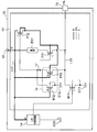
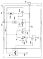
- FIG. 3 is a circuit diagram of the sensor device according to the first embodiment.
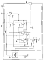
- FIG. Explanatory drawing at the time of normal operation which concerns on 1st Embodiment.
- the circuit diagram of the sensor apparatus concerning a 2nd embodiment.
- the circuit diagram of the sensor device concerning a 3rd embodiment.
- the circuit diagram of the sensor device concerning a 4th embodiment.
- the circuit diagram of the sensor device concerning a 5th embodiment.
- the circuit diagram of the sensor apparatus concerning a 6th embodiment.
- FIG. 1 is a circuit diagram of the sensor device according to the first embodiment.
- the sensor device may be, for example, an air flow sensor, but is not particularly limited as long as it is a device whose electrical characteristics change according to a physical quantity.
- the sensor device 10 is connected to a host device such as an ECU (not shown) via a power supply terminal 12 and a signal terminal 13, and an LSI internal circuit (detection circuit) in which a sensor element is mounted. 14 and a control circuit 11 that processes a detection signal from the sensor element.
- the LSI internal circuit 14 is connected to a power supply line L11 connected to the power supply terminal 12, and receives a power supply voltage from a host device through the power supply line L11 to operate the sensor element and the like. Further, the LSI internal circuit 14 performs various processes on the physical quantity detected by the sensor element, and outputs a control signal according to the physical quantity to the control circuit 11.
- the control circuit 11 receives the power supply voltage from the host device via the power supply line L11 connected to the power supply terminal 12, and outputs the output signal corresponding to the control signal of the LSI internal circuit 14 via the signal line L12 connected to the signal terminal 13 Outputting to the device.
- the control circuit 11 is provided with a first NMOS transistor N11 for driving the circuit between the signal line L12 and the ground G11.
- P11 and a second PMOS transistor (second transistor) P12 for well control provided between the well of the first PMOS transistor P11 and the power supply line L11 are provided.
- control circuit 11 is provided with a gate control circuit 15 that shuts off the first and second PMOS transistors P11 and P12 when the power is cut off.
- the gate control circuit 15 is provided with a second NMOS transistor N12 and a third PMOS transistor P13.
- the second NMOS transistor N12 is provided between the connection point 17 of the gate terminal of the first PMOS transistor P11 and the gate terminal of the second PMOS transistor P12 and the ground G12.
- the third PMOS transistor P13 is provided between the signal line L12 and a connection point 17 between the gate terminal of the first PMOS transistor P11 and the gate terminal of the second PMOS transistor P12.
- the drain terminal of the first NMOS transistor N11 for driving the circuit is connected to the signal line L12, and the source terminal of the first NMOS transistor N11 is connected to the ground G11.
- the LSI internal circuit 14 is connected to the gate terminal of the first NMOS transistor N11, and the first NMOS transistor N11 is driven by receiving a control signal from the LSI internal circuit 14.
- the first NMOS transistor N11 is ON / OFF driven in response to a control signal from the LSI internal circuit 14 to generate an output signal according to a physical quantity detected by a sensor element in the LSI internal circuit 14.
- the first PMOS transistor P11 for cutting off current has one input / output terminal connected to the load R11 and the other input / output terminal connected to the signal line L12.
- the first PMOS transistor P11 is used to disconnect the current path from the signal line L12 to the power supply line L11.
- the second PMOS transistor P12 for well control has one input / output terminal connected to the power supply line L11 and the other input / output terminal connected to the wells of the first to third PMOS transistors P11 to P13.
- the second PMOS transistor P12 fixes the well potentials of the first to third PMOS transistors P11 to P13 at a constant level.
- the drain terminal of the second NMOS transistor N12 of the gate control circuit 15 is connected to the gate terminals of the first and second PMOS transistors P11 and P12, and the source terminal is connected to its own well and the ground G12.
- the gate terminal of the second NMOS transistor N12 is connected to the power supply line L11.
- the second NMOS transistor N12 is turned on during the normal operation in which the gate potential of the second NMOS transistor N12 is the power supply potential.
- the gate terminals of the first and second PMOS transistors P11 and P12 are connected to the ground G12, and the first and second PMOS transistors P11 and P12 become conductive.
- the third PMOS transistor P13 of the gate control circuit 15 has one input / output terminal connected to the gate terminals of the first and second PMOS transistors P11 and P12 and the other input / output terminal connected to the signal line L12. There is.
- the gate terminal of the third PMOS transistor P13 is connected to the power supply line L11.
- the gate potential of the third PMOS transistor P13 is the ground potential and the power is disconnected, the third PMOS transistor P13 becomes conductive.
- the gate terminals of the first and second PMOS transistors P11 and P12 are connected to the signal line L12, and the first and second PMOS transistors P11 and P12 are cut off.
- the gate control circuit 15 prevents the current from flowing from the signal line L12 to the power supply line L11 when the power supply is cut off, and the first and second PMOS transistors P11 and P12 are cut off when the power supply is cut off. Is shut off.
- the first PMOS transistor P11 disconnects the DC path from the signal line L12 to the power supply line L11.
- the second PMOS transistor P12 disconnects the current path from the signal line L12 to the power supply line L11 through the parasitic diodes D1 and D2 (see FIG. 3) of the first and third PMOS transistors P11 and P13.
- FIG. 2 is an explanatory diagram of a normal operation according to the first embodiment.
- FIG. 3 is an explanatory diagram when the power source is disconnected according to the first embodiment.
- the power supply voltage is applied to the gate terminal of the second NMOS transistor N12 and the gate terminal of the third PMOS transistor P13 of the gate control circuit 15.
- the gate potential of the second NMOS transistor N12 becomes the power supply potential to render the second NMOS transistor N12 conductive
- the gate potential of the third PMOS transistor P13 becomes the power supply potential to shut off the third PMOS transistor P13.
- the gate terminals of the first and second PMOS transistors P11 and P12 are connected to the ground G12.
- the gate potentials of the first and second PMOS transistors P11 and P12 become the ground potential, the well potentials of the first and second PMOS transistors P11 and P12 are fixed to the power supply potential, and the first and second PMOS transistors P11 and P12 are fixed.
- the conduction state of P11 and P12 is maintained.
- the first PMOS transistor P11 one input / output terminal connected to the load R11 functions as a source, and the other input / output terminal connected to the signal line L12 functions as a drain.
- the second PMOS transistor P12 one input / output terminal connected to the power supply line L11 functions as a source, and the other input / output terminal connected to the wells of the PMOS transistors P11-P13 functions as a drain.
- the conduction of the second PMOS transistor P12 fixes the well potential of the third PMOS transistor P13 to the power supply potential, and the cutoff state of the third PMOS transistor P13 is maintained. This prevents the signal line L12 from being connected to the ground G12 via the third PMOS transistor P13 and the second NMOS transistor N12.
- the gate terminal of the first PMOS transistor P11 is connected to the ground G12, and the well potential of the first PMOS transistor P11 is set to the power supply potential, so that the first PMOS transistor P11 is in the conductive state. Has been maintained.
- the gate terminal of the second NMOS transistor N12 and the gate terminal of the third PMOS transistor P13 of the gate control circuit 15 are connected to the ground G13 via the load of the LSI internal circuit 14. .
- the gate potential of the second NMOS transistor N12 becomes the ground potential
- the second NMOS transistor N12 is cut off
- the gate potential of the third PMOS transistor P13 becomes the ground potential
- the third PMOS transistor P13 becomes conductive.
- the second NMOS transistor N12 is cut off and the third PMOS transistor P13 is turned on, so that the gate terminals of the first and second PMOS transistors P11 and P12 are connected to the signal line L12.
- the gate potentials of the first and second PMOS transistors P11 and P12 become the signal potential through the third PMOS transistor P13. Further, the well potentials of the first to third PMOS transistors P11 to P13 are fixed to potentials lower than the signal potential by the parasitic diode D1 of the first PMOS transistor P11. In this case, the threshold voltages of the first and second PMOS transistors P11 and P12 are lowered, but the gate-source voltages of the first and second PMOS transistors P11 and P12 are lower than the threshold voltage, so that the first , The second PMOS transistors P11 and P12 are maintained in the cutoff state.
- the source-drain of the pair of input / output terminals of the first PMOS transistor P11 is switched from the normal operation, and the source-drain of the pair of input / output terminals of the second PMOS transistor P12 is switched.
- the first PMOS transistor P11 one input / output terminal connected to the load R11 functions as a drain, and the other input / output terminal connected to the signal line L12 functions as a source.
- the second PMOS transistor P12 one input / output terminal connected to the power supply line L11 functions as a drain, and the other input / output terminal connected to the well of each PMOS transistor P11-P13 functions as a source.
- the DC path of the current flowing from the signal line L12 to the power supply line L11 is cut off.
- a current path is formed in the first PMOS transistor P11 by the parasitic diode D1 shown by the broken line, but the second PMOS transistor P12 is maintained in the cutoff state, so that the power is supplied from the signal line L12 through the parasitic diode D1.
- the current path toward the line L11 is cut off.
- a current path is also formed in the third PMOS transistor P13 by the parasitic diode D2 indicated by the broken line, but a current path from the signal line L12 to the power supply line L11 via the parasitic diode D2 by the second PMOS transistor P12. Is disconnected.
- the second PMOS transistor P12 controls the wells of the PMOS transistors P11 to P13 and disconnects the current paths of the parasitic diodes D1 and D2 of the first and third PMOS transistors P11 and P13. Therefore, it is not necessary to separately prepare transistors for well control of the first and third PMOS transistors P11 and P13 and disconnection of the current paths of the parasitic diodes D1 and D2. By making the wells of the PMOS transistors P11 to P13 common, it is possible to reduce the area of the chip. In this embodiment, the transistors may be individually prepared for the well control of the first and third PMOS transistors P11 and P13.
- the gate potentials of the first and second PMOS transistors P11 and P12 become signal potentials when the power is cut off, and the well potentials of the first and second PMOS transistors P11 and P12 change. It is fixed at a predetermined potential.
- the first PMOS transistor P11 is cut off, and the DC path from the signal line L12 to the power supply line L11 is cut off.
- the second PMOS transistor P12 is cut off, and the current path from the signal line L12 to the power supply line L11 is cut off through the parasitic diodes D1 and D2 of the first and third PMOS transistors P11 and P13.
- the sneak of the current flowing from the signal line L12 to the power supply line L11 is suppressed and the output of the intermediate potential is prevented.
- the damage to the LSI and the erroneous diagnosis of the output signal by the host device are suppressed.
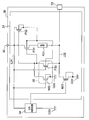
- FIG. 4 is a circuit diagram of the sensor device according to the second embodiment.
- the sensor device 20 according to the second embodiment is different from that of the first embodiment in that a fourth PMOS transistor P24 is provided for well control when the power is cut off. That is, the control circuit 21 is provided with the load R21, the first and second NMOS transistors N21 and N22, and the first to third PMOS transistors P21 to P23, like the control circuit 11 of the first embodiment. ing. In addition, the control circuit 21 includes a fourth PMOS transistor P24 for well control at the time of power supply disconnection between the signal line L22 and a connection point 28 between the well of the first PMOS transistor P21 and the well of the second PMOS transistor P22. Is provided.
- the fourth PMOS transistor P24 has one input / output terminal connected to the well of each PMOS transistor P21-P24, and the other input / output terminal connected to the signal line L22.
- the gate terminal of the fourth PMOS transistor P24 is connected to the power supply line L21.
- one input / output terminal connected to the well of each PMOS transistor P21-P24 functions as a source
- the other input / output terminal connected to the signal line L22 functions as a drain in the normal operation.
- one input / output terminal connected to the wells of the PMOS transistors P21-P24 functions as a drain
- the other input / output terminal connected to the signal line L22 functions as a source.
- the power supply voltage is applied to the gate terminal of the fourth PMOS transistor P24, and the gate potential of the fourth PMOS transistor P24 becomes the power supply potential.
- the second PMOS transistor P22 becomes conductive, the well potential of the fourth PMOS transistor P24 is fixed to the power supply potential, and the cutoff state of the fourth PMOS transistor P24 is maintained.
- the control circuit 21 of the second embodiment operates similarly to the control circuit 11 of the first embodiment, so that the operation of the control circuit 21 is adversely affected by the addition of the fourth PMOS transistor P24. There is no.
- the gate terminal of the fourth PMOS transistor P24 is connected to the ground G23 via the load of the LSI internal circuit 24.
- the gate potential of the fourth PMOS transistor P24 becomes the ground potential, and the well potentials of the first to third PMOS transistors P21 to P23 are fixed to the signal potential through the fourth PMOS transistor P24.
- the voltage drop corresponding to the parasitic diode of the first PMOS transistor P21 as in the first embodiment is eliminated, and the threshold voltages of the first and second PMOS transistors P21 and P22 increase, so that the current is cut off. Leakage current can be reduced.
- the fourth PMOS transistor P24 can enhance the current interruption effect of the first and second PMOS transistors P21 and P22.
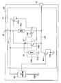
- FIG. 5 is a circuit diagram of the sensor device according to the third embodiment.
- the sensor device 30 according to the third embodiment is different from the first embodiment in that the positions of the first PMOS transistor P31 and the load R31 are exchanged. That is, the control circuit 31 is provided with the load R31, the first and second NMOS transistors N31 and N32, and the first to third PMOS transistors P31 to P33, as in the control circuit 11 of the first embodiment. ing. Since the first PMOS transistor P31 is provided between the power supply line L31 and the load R31, the gate-source voltage of the first PMOS transistor P31 increases during normal operation. Therefore, the ON resistance of the first PMOS transistor P31 can be reduced and the area of the chip can be reduced.
- the third embodiment it is possible to suppress the sneak of the current flowing from the signal line L32 to the power supply line L31 at the time of the power supply disconnection, as in the first embodiment. Further, it is possible to reduce the area of the chip of the first PMOS transistor P31.
- the second NMOS transistor is used as the first element of the gate control circuit and the third PMOS transistor is used as the second element, but the present invention is not limited to this configuration.
- the gate control circuit connects the first element that connects the gate terminals of the first and second PMOS transistors to the ground during normal operation, and connects the gate terminals of the first and second PMOS transistors to the signal line when the power is disconnected.
- the second element may be provided.
- the first element of the gate control circuit may be composed of a resistor.
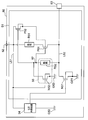
- FIG. 6 is a circuit diagram of the sensor device according to the fourth embodiment.
- the sensor device 40 according to the fourth embodiment is different from the first embodiment in that the second NMOS transistor N12 (see FIG. 1) is replaced with a resistor R42. That is, the control circuit 41 is provided with the load R41, the first NMOS transistor N41, and the first to third PMOS transistors P41 to P43, as in the control circuit 11 of the first embodiment.
- the resistor R42 of the gate control circuit 45 is provided between the connection point 47 of the gate terminals of the first and second PMOS transistors P41 and P42 and the ground G42.
- the resistance value of the resistor R42 is set to be larger than the resistance value of the ON resistance of the third PMOS transistor P43.
- the power supply voltage is applied to the gate terminal of the third PMOS transistor P43 of the gate control circuit 45.
- the gate potential of the third PMOS transistor P43 becomes the power supply potential, and the third PMOS transistor P43 is cut off. Therefore, the gate terminals of the first and second PMOS transistors P41 and P42 are connected to the ground G42 via the resistor R42.
- the gate potentials of the first and second PMOS transistors P41 and P42 become the ground potential, and the well potentials of the first and second PMOS transistors P41 and P42 are fixed to the power supply potential, so that the first and second PMOS transistors P41 and P42 are fixed. The conduction state of P41 and P42 is maintained.
- the gate terminal of the third PMOS transistor P43 of the gate control circuit 45 is connected to the ground G43 via the load of the LSI internal circuit 44.
- the gate potential of the third PMOS transistor P43 becomes the ground potential, and the third PMOS transistor P43 becomes conductive. Since the third PMOS transistor P43 is conductive and the resistance value of the resistor R42 is set high, the gate terminals of the first and second PMOS transistors P41 and P42 are connected to the signal line L42.
- the gate potentials of the first and second PMOS transistors P41 and P42 become signal potentials, and the cutoff states of the first and second PMOS transistors P41 and P42 are maintained.
- the gate control circuit 45 can be composed of the resistor R42 and the third PMOS transistor P43.
- the second element of the gate control circuit may be composed of a resistor.
- a sensor device according to the fifth embodiment will be described with reference to FIG. 7.
- the sensor device according to the fifth embodiment uses an NMOS transistor as the first element of the gate control circuit and a resistor as the second element.
- the description of the same configuration as the first embodiment is omitted as much as possible.
- FIG. 7 is a circuit diagram of the sensor device according to the fifth embodiment.
- the sensor device 50 according to the fifth embodiment is different from the first embodiment in that the third PMOS transistor P13 (see FIG. 1) is replaced with a resistor R52. That is, the control circuit 51 is provided with the load R51, the first and second NMOS transistors N51 and N52, and the first and second PMOS transistors P51 and P52 as in the control circuit 11 of the first embodiment. ing.
- the resistor R52 of the gate control circuit 55 is provided between the connection point 57 of the gate terminals of the first and second PMOS transistors P51 and P52 and the signal line L52. Further, the resistance value of the resistor R52 is set to be larger than the resistance value of the combined resistance of the load R51 and the ON resistance of the first PMOS transistor P51.
- the power supply voltage is applied to the gate terminal of the second NMOS transistor N52 of the gate control circuit 55.
- the gate potential of the second NMOS transistor N52 becomes the power supply potential, and the second NMOS transistor N52 becomes conductive. Since the resistance value of the resistor R52 is set to be high, the gate terminals of the first and second PMOS transistors P51 and P52 are connected to the ground G52 via the second NMOS transistor N52.
- the gate potentials of the first and second PMOS transistors P51 and P52 become the ground potential, the well potentials of the first and second PMOS transistors P51 and P52 are fixed to the power supply potential, and the first and second PMOS transistors P51 and P52 are fixed. The conduction state of P51 and P52 is maintained.
- the gate terminal of the second NMOS transistor N52 of the gate control circuit 55 is connected to the ground G53 via the load of the LSI internal circuit 54.
- the gate potential of the second NMOS transistor N52 becomes the ground potential, and the second NMOS transistor N52 is cut off.
- the gate terminals of the first and second PMOS transistors P51 and P52 are connected to the signal line L52 via the resistor R52.
- the gate potentials of the first and second PMOS transistors P51 and P52 increase, and the cutoff states of the first and second PMOS transistors P51 and P52 are maintained.
- the gate control circuit 55 can be composed of the second NMOS transistor N52 and the resistor R52.
- FIG. 8 is a circuit diagram of the sensor device according to the sixth embodiment.
- the sensor device 60 according to the sixth embodiment is different from the second embodiment in that the second PMOS transistor P22 for well control (see FIG. 4) is replaced with a resistor R62. is doing. That is, as in the control circuit 21 of the second embodiment, the control circuit 61 includes the load R61, the first and second NMOS transistors N61 and N62, the first, third and fourth PMOS transistors P61 and P63. , P64 are provided. The well control resistor R62 is provided between the power supply line L61 and the fourth PMOS transistor P64. The resistance value of the resistor R62 is set to be larger than the resistance value of the pull-up resistor of a host device such as an ECU (not shown).
- the power supply voltage is applied to the gate terminal of the fourth PMOS transistor P64, and the gate potential of the fourth PMOS transistor P64 becomes the power supply potential. Since the fourth PMOS transistor P64 is cut off, the well potential of the first, third, and fourth PMOS transistors P61, P63, and P64 is fixed to a high potential via the well control resistor R62. The conduction state of the first PMOS transistor P61 is maintained, and the cutoff states of the third and fourth PMOS transistors P63 and P64 are maintained. Thus, the well potential of each of the PMOS transistors P61, P63, P64 can be controlled by the resistor R62 and the fourth PMOS transistor P64 as in the control circuit 11 of the first embodiment.
- the gate terminal of the fourth PMOS transistor P64 is connected to the ground G63 via the load of the LSI internal circuit 64.
- the gate potential of the fourth PMOS transistor P64 becomes the ground potential, and the fourth PMOS transistor P64 becomes conductive. Since the resistance value of the resistor R62 is set high, the well potentials of the first, third, and fourth PMOS transistors P61, P63, and P64 are fixed to the signal potential through the fourth PMOS transistor P64.
- the voltage drop corresponding to the parasitic diode of the first PMOS transistor P61 as in the first embodiment is eliminated, and the threshold voltage of the first PMOS transistor P61 is increased to cut off the current as in the second embodiment.
- the leak current can be reduced.
- the sixth embodiment it is possible to suppress the sneak of the current flowing from the signal line L62 to the power supply line L61 when the power supply is disconnected, as in the second embodiment. Further, the well potential of the first, third, and fourth PMOS transistors P61, P63, and P64 can be controlled by the resistor R62 and the fourth PMOS transistor P64.
- FIG. 9 is a circuit diagram of the sensor device according to the seventh embodiment.
- the sensor device 70 according to the seventh embodiment differs from the sensor device 70 according to the second embodiment in that the well controlling fourth PMOS transistor P24 (see FIG. 4) is replaced with a resistor R72. is doing. That is, the control circuit 71 is provided with the load R71, the first and second NMOS transistors N71 and N72, and the first to third PMOS transistors P71 to P73, as in the control circuit 21 of the second embodiment. ing.
- the well controlling resistor R72 is provided between the second PMOS transistor P72 and the signal line L72.
- the gate terminal of the second PMOS transistor P72 is connected to the ground G72 through the second NMOS transistor N72 of the gate control circuit 75, and the gate potential of the second PMOS transistor P72 becomes the ground potential. Therefore, the well potentials of the first to third PMOS transistors P71 to P73 are fixed to the power supply potential via the second PMOS transistor P72. The conduction state of the first and second PMOS transistors P71 and P72 is maintained, and the cutoff state of the third PMOS transistor P73 is maintained.
- the first and second PMOS transistors P71 and P72 become conductive, and the series circuit of the load R71 and the first PMOS transistor P71 and the second PMOS transistor P72 are connected between the power supply line L71 and the signal line L72. And a resistor R72 in series are formed in parallel. Therefore, by dividing the resistance value of the combined resistance of the parallel circuit including the two series circuits and the resistance value of the ON resistance of the first NMOS transistor N71 for driving the circuit, the reference of the low voltage of the host device is satisfied. Is set to the resistance value of each element of the parallel circuit.
- the second PMOS transistor P72 When the power is cut off, the second PMOS transistor P72 is cut off, and the well potential of the first to third PMOS transistors P71 to P73 is controlled by the resistor R72. As a result, the well potential of each of the PMOS transistors P71-P73 can be controlled by the second PMOS transistor P72 and the resistor R72, as in the control circuit 21 of the second embodiment.
- the seventh embodiment it is possible to suppress the sneak of the current flowing from the signal line L72 to the power supply line L71 at the time of power supply disconnection, as in the second embodiment. Also, the well potentials of the first to third PMOS transistors P71 to P73 can be controlled by the second PMOS transistor P72 and the resistor R72.
- the control circuit is provided with a load, but the load may be formed of a resistor or a transistor.
- the load may be composed of PMOS transistors.
- the sensor device according to the eighth embodiment will be described with reference to FIG. 10. Here, the description of the same configuration as the first embodiment is omitted as much as possible.
- FIG. 10 is a circuit diagram of the sensor device according to the eighth embodiment.
- the sensor device 80 differs from that of the first embodiment in that a fifth PMOS transistor P85 is provided as a current adjustment load. That is, the control circuit 81 is provided with the first and second NMOS transistors N81 and N82 and the first to third PMOS transistors P81 to P83, similarly to the control circuit 11 of the first embodiment. Further, the control circuit 81 is provided with a fifth PMOS transistor P85 for current adjustment between the power supply line L81 and the first PMOS transistor P81. By configuring the load with a transistor, the effect of adjusting the current is enhanced.
- the fifth PMOS transistor P85 has one input / output terminal (source terminal) connected to the power supply line L81 and the other input / output terminal (drain terminal) connected to one input / output terminal of the first PMOS transistor P81. ing.
- the LSI internal circuit 84 is connected to the gate terminal of the fifth PMOS transistor P85, and the fifth PMOS transistor P85 is driven by receiving a control signal from the LSI internal circuit 84.
- the well potential of the fifth PMOS transistor P85 is controlled by the second PMOS transistor P82. Therefore, the wells of the PMOS transistors P81-P83 and P85 can be shared to reduce the area of the chip.
- the eighth embodiment it is possible to suppress the sneak of the current flowing from the signal line L82 to the power supply line L81 at the time of the power supply disconnection, as in the first embodiment. Further, by using the fifth PMOS transistor P85 as the load, the effect of adjusting the current can be enhanced.
- each sensor of this embodiment may be controlled by a pull-up circuit in order to comply with the SENT (Signal Edge Nibble Transmission) standard. Even if the power supply is disconnected while the signal potential is always pulled up without using the pull-up circuit, it is possible to prevent the current from flowing from the signal line to the power supply line and prevent the output of the intermediate potential.
- SENT Synignal Edge Nibble Transmission
Landscapes
- Physics & Mathematics (AREA)
- Nonlinear Science (AREA)
- Fluid Mechanics (AREA)
- General Physics & Mathematics (AREA)
- Electronic Switches (AREA)
- Semiconductor Integrated Circuits (AREA)
- Logic Circuits (AREA)
Abstract
Description
以下、図1から図3を参照して、第1の実施形態に係るセンサ装置について説明する。
図1は、第1の実施形態に係るセンサ装置の回路図である。なお、センサ装置としては、例えばエアフローセンサが挙げられるが、物理量に応じて電気的特性の変化する装置であれば特に限定されない。
また、第1-第3のPMOSトランジスタP11-P13のウェル電位が第1のPMOSトランジスタP11の寄生ダイオードD1分だけ信号電位から低下した電位に固定される。この場合、第1、第2のPMOSトランジスタP11、P12の閾値電圧が低下するが、閾値電圧よりも第1、第2のPMOSトランジスタP11、P12のゲート-ソース間電圧が低くなるため、第1、第2のPMOSトランジスタP11、P12が遮断状態で維持される。
図4を参照して、第2の実施形態に係るセンサ装置について説明する。第1の実施形態では、電源断線時に各PMOSトランジスタのウェル電位が寄生ダイオード分だけ信号電位から低下した電位に固定される。このため、閾値電圧が下がって電流遮断時のリーク電流が僅かに生じる場合がある。そこで、第2の実施形態に係るセンサ装置は、電源断線時のウェル制御用に第4のPMOSトランジスタを備えている。ここでは、第1の実施形態と同様な構成については説明を極力省略する。図4は、第2の実施形態に係るセンサ装置の回路図である。
第4のPMOSトランジスタP24のゲート端子は電源線L21に接続されている。第4のPMOSトランジスタP24では、通常動作時に各PMOSトランジスタP21-P24のウェルに連なる一方の入出力端子がソースとして働き、信号線L22に連なる他方の入出力端子がドレインとして働いている。電源断線時に各PMOSトランジスタP21-P24のウェルに連なる一方の入出力端子がドレインとして働き、信号線L22に連なる他方の入出力端子がソースとして働いている。
図5を参照して、第3の実施形態に係るセンサ装置について説明する。第1の実施形態では、負荷と信号線の間に第1のPMOSトランジスタを設けているため、負荷によって第1のPMOSトランジスタのゲート-ソース間電圧が小さくなってチップの小面積化を十分に図ることができなかった。そこで、第3の実施形態に係るセンサ装置は、電源線と負荷の間に第1のPMOSトランジスタを設けている。ここでは、第1の実施形態と同様な構成については説明を極力省略する。図5は、第3の実施形態に係るセンサ装置の回路図である。
上記した各実施形態では、ゲート制御回路の第1の素子として第2のNMOSトランジスタ、第2の素子として第3のPMOSトランジスタを例示したが、この構成に限定されない。ゲート制御回路は、通常動作時に第1、第2のPMOSトランジスタのゲート端子をグランドに接続する第1の素子と、電源断線時に第1、第2のPMOSトランジスタのゲート端子を信号線に接続する第2の素子を備えていればよい。例えば、図6に示すように、ゲート制御回路の第1の素子を抵抗で構成してもよい。
また、抵抗R42の抵抗値は第3のPMOSトランジスタP43のON抵抗の抵抗値よりも大きく設定されている。
また、図7に示すように、ゲート制御回路の第2の素子を抵抗で構成してもよい。図7を参照して、第5の実施形態に係るセンサ装置について説明する。第5の実施形態に係るセンサ装置は、ゲート制御回路の第1の素子としてNMOSトランジスタを使用し、第2の素子として抵抗を使用している。ここでは、第1の実施形態と同様な構成については説明を極力省略する。図7は、第5の実施形態に係るセンサ装置の回路図である。
上記した第2の実施形態では、第2、第4のPMOSトランジスタによってウェル制御する構成を例示したが、この構成に限定されない。例えば、図8に示すように、通常動作時に導通する第2のPMOSトランジスタを抵抗に置き換えてもよい。図8を参照して、第6の実施形態に係るセンサ装置について説明する。ここでは、第2の実施形態と同様な構成については説明を極力省略する。図8は、第6の実施形態に係るセンサ装置の回路図である。
また、図9に示すように、電源断線時に導通する第4のPMOSトランジスタを抵抗に置き換えてもよい。図9を参照して、第7の実施形態に係るセンサ装置について説明する。ここでは、第2の実施形態と同様な構成については説明を極力省略する。図9は、第7の実施形態に係るセンサ装置の回路図である。
これにより、第2のPMOSトランジスタP72と抵抗R72によって、第2の実施形態の制御回路21と同様に、各PMOSトランジスタP71-P73のウェル電位を制御できる。
上記した各実施形態では、制御回路に負荷が設けられる構成にしたが、負荷は抵抗で構成されていてもよいし、トランジスタで構成されていてもよい。例えば、図10に示すように、負荷をPMOSトランジスタで構成してもよい。図10を参照して、第8の実施形態に係るセンサ装置について説明する。ここでは、第1の実施形態と同様な構成については説明を極力省略する。図10は、第8の実施形態に係るセンサ装置の回路図である。
11、21、31、41、51、61、71、81 制御回路
14、24、34、44、54、64、74、84 LSI内部回路(検出回路)
15、45、55、75 ゲート制御回路
L11、L21、L31、L41、L51、L61、L71、L81 電源線L12、L22、L32、L42、L52、L62、L72、L82 信号線
N12、N22、N32、N52、N62、N72、N82 第2のNMOSトランジスタ
P11、P21、P31、P41、P51、P61、P71、P81 第1のPMOSトランジスタ(第1のトランジスタ)
P12、P22、P32、P42、P52、P72、P82 第2のPMOSトランジスタ(第2のトランジスタ)
P13、P23、P33、P43、P63,P73、P83 第3のPMOSトランジスタ
P24、P64 第4のPMOSトランジスタ
P85 第5のPMOSトランジスタ
R11、R21、R31、R41、R51、R61、R71 負荷
R42、R52、R62、R72 抵抗
Claims (12)
- 電源線からの電源電圧を受けて出力信号を信号線に出力する制御回路であって、
前記電源線と前記信号線の間に設けられた負荷と、
前記負荷と前記信号線の間又は前記電源線と前記負荷の間に設けられた第1のトランジスタと、
前記第1のトランジスタのウェルと前記電源線の間に設けられた第2のトランジスタと、
電源断線時に前記第1のトランジスタのゲート端子及び前記第2のトランジスタのゲート端子を前記信号線に接続し、前記第1のトランジスタ及び前記第2のトランジスタを遮断するゲート制御回路とを備えたことを特徴とする制御回路。 - 前記ゲート制御回路は、
通常動作時には前記第1のトランジスタのゲート端子及び前記第2のトランジスタのゲート端子をグランドに接続し、前記第2のトランジスタを介して前記第1のトランジスタのウェル電位を電源電位にすることで前記第1のトランジスタを導通させることを特徴とする請求項1に記載の制御回路。 - 前記第1のトランジスタは第1のPMOSトランジスタであり、
前記第2のトランジスタは第2のPMOSトランジスタであり、
前記ゲート制御回路は、前記第1のPMOSトランジスタのゲート端子及び前記第2のPMOSトランジスタのゲート端子の接続点とグランドとの間に設けられた第1の素子と、
前記第1のPMOSトランジスタのゲート端子及び前記第2のPMOSトランジスタのゲート端子の接続点と前記信号線との間に設けられた第2の素子とを有し、
通常動作時に前記第1の素子を介して前記第1のPMOSトランジスタのゲート端子及び前記第2のPMOSトランジスタのゲート端子をグランドに接続し、電源断線時に前記第2の素子を介して前記第1のPMOSトランジスタのゲート端子及び前記第2のPMOSトランジスタのゲート端子を前記信号線に接続することを特徴とする請求項1に記載の制御回路。 - 前記第1の素子はNMOSトランジスタであり、前記第2の素子は第3のPMOSトランジスタであり、
前記NMOSトランジスタのゲート端子は前記電源線に接続され、前記第3のPMOSトランジスタのゲート端子は前記電源線に接続されたことを特徴とする請求項3に記載の制御回路。 - 前記第2のPMOSトランジスタの一方の入出力端子は前記電源線に接続され、前記第2のPMOSトランジスタの他方の入出力端子は前記第1のPMOSトランジスタのウェル、前記第2のPMOSトランジスタのウェル、前記第3のPMOSトランジスタのウェルに接続されたことを特徴とする請求項4に記載の制御回路。
- 前記第1のPMOSトランジスタのウェルと前記第2のPMOSトランジスタのウェルの接続点と前記信号線との間に設けられた第4のPMOSトランジスタを備え、
前記第4のPMOSトランジスタのゲート端子は前記電源線に接続されたことを特徴とする請求項5に記載の制御回路。 - 前記第4のPMOSトランジスタの一方の入出力端子は前記第1のPMOSトランジスタのウェル、前記第2のPMOSトランジスタのウェル、前記第3のPMOSトランジスタのウェル、前記第4のPMOSトランジスタのウェルに接続され、前記第4のPMOSトランジスタの他方の入出力端子は前記信号線に接続されたことを特徴とする請求項6に記載の制御回路。
- 前記第2のPMOSトランジスタ及び前記第4のPMOSトランジスタのいずれか一方を抵抗に置き換えたことを特徴とする請求項7に記載の制御回路。
- 前記第1の素子は抵抗であり、前記第2の素子は第3のPMOSトランジスタであり、
前記第3のPMOSトランジスタのゲート端子は前記電源線に接続されたことを特徴とする請求項3に記載の制御回路。 - 前記第1の素子はNMOSトランジスタであり、前記第2の素子は抵抗であり、
前記NMOSトランジスタのゲート端子は前記電源線に接続されたことを特徴とする請求項3に記載の制御回路。 - 前記負荷が抵抗又はトランジスタで構成されたことを特徴とする請求項1に記載の制御回路。
- 請求項1から請求項11のいずれか一項に記載の制御回路と、
前記制御回路に物理量に応じた制御信号を出力する検出回路とを備えたことを特徴とするセンサ装置。
Priority Applications (4)
| Application Number | Priority Date | Filing Date | Title |
|---|---|---|---|
| CN201980060766.XA CN112840567B (zh) | 2018-10-18 | 2019-09-13 | 控制电路以及传感器装置 |
| US17/286,243 US11271554B2 (en) | 2018-10-18 | 2019-09-13 | Control circuit and sensor device |
| DE112019004614.4T DE112019004614B4 (de) | 2018-10-18 | 2019-09-13 | Steuerschaltung und sensorvorrichtung |
| JP2020552965A JP7062079B2 (ja) | 2018-10-18 | 2019-09-13 | 制御回路及びセンサ装置 |
Applications Claiming Priority (2)
| Application Number | Priority Date | Filing Date | Title |
|---|---|---|---|
| JP2018196295 | 2018-10-18 | ||
| JP2018-196295 | 2018-10-18 |
Publications (1)
| Publication Number | Publication Date |
|---|---|
| WO2020080004A1 true WO2020080004A1 (ja) | 2020-04-23 |
Family
ID=70283443
Family Applications (1)
| Application Number | Title | Priority Date | Filing Date |
|---|---|---|---|
| PCT/JP2019/036025 Ceased WO2020080004A1 (ja) | 2018-10-18 | 2019-09-13 | 制御回路及びセンサ装置 |
Country Status (5)
| Country | Link |
|---|---|
| US (1) | US11271554B2 (ja) |
| JP (1) | JP7062079B2 (ja) |
| CN (1) | CN112840567B (ja) |
| DE (1) | DE112019004614B4 (ja) |
| WO (1) | WO2020080004A1 (ja) |
Citations (3)
| Publication number | Priority date | Publication date | Assignee | Title |
|---|---|---|---|---|
| JPH10224201A (ja) * | 1997-02-03 | 1998-08-21 | Fujitsu Ltd | 半導体集積回路装置 |
| JP2016192838A (ja) * | 2015-03-31 | 2016-11-10 | 日立オートモティブシステムズ株式会社 | センサ装置 |
| JP2018011387A (ja) * | 2016-07-11 | 2018-01-18 | ミツミ電機株式会社 | 保護ic及び半導体集積回路 |
Family Cites Families (10)
| Publication number | Priority date | Publication date | Assignee | Title |
|---|---|---|---|---|
| JP4559643B2 (ja) * | 2000-02-29 | 2010-10-13 | セイコーインスツル株式会社 | ボルテージ・レギュレータ、スイッチング・レギュレータ、及びチャージ・ポンプ回路 |
| CN100452654C (zh) * | 2003-11-05 | 2009-01-14 | 中芯国际集成电路制造(上海)有限公司 | 用于高电压输入的上拉晶体管的栅极控制电路 |
| JP5266029B2 (ja) * | 2007-12-14 | 2013-08-21 | ルネサスエレクトロニクス株式会社 | 負荷駆動装置 |
| JP2011089850A (ja) * | 2009-10-21 | 2011-05-06 | Asahi Kasei Electronics Co Ltd | 断線検出・逆接続保護装置 |
| JP2013124879A (ja) * | 2011-12-13 | 2013-06-24 | Panasonic Corp | センサ装置 |
| JP2014045464A (ja) * | 2012-08-29 | 2014-03-13 | Renesas Electronics Corp | 入出力回路、半導体装置およびバス通信システム |
| JP5619253B1 (ja) * | 2013-10-15 | 2014-11-05 | 三菱電機株式会社 | 誘導性負荷の給電制御装置 |
| JP5749821B2 (ja) * | 2014-02-13 | 2015-07-15 | ルネサスエレクトロニクス株式会社 | 半導体装置 |
| JP6042962B2 (ja) * | 2015-11-27 | 2016-12-14 | ルネサスエレクトロニクス株式会社 | 差動出力回路および半導体装置 |
| CN110402493B (zh) * | 2016-12-26 | 2023-01-13 | 德州仪器公司 | 动态触发式静电放电单元 |
-
2019
- 2019-09-13 US US17/286,243 patent/US11271554B2/en active Active
- 2019-09-13 DE DE112019004614.4T patent/DE112019004614B4/de active Active
- 2019-09-13 JP JP2020552965A patent/JP7062079B2/ja active Active
- 2019-09-13 CN CN201980060766.XA patent/CN112840567B/zh active Active
- 2019-09-13 WO PCT/JP2019/036025 patent/WO2020080004A1/ja not_active Ceased
Patent Citations (3)
| Publication number | Priority date | Publication date | Assignee | Title |
|---|---|---|---|---|
| JPH10224201A (ja) * | 1997-02-03 | 1998-08-21 | Fujitsu Ltd | 半導体集積回路装置 |
| JP2016192838A (ja) * | 2015-03-31 | 2016-11-10 | 日立オートモティブシステムズ株式会社 | センサ装置 |
| JP2018011387A (ja) * | 2016-07-11 | 2018-01-18 | ミツミ電機株式会社 | 保護ic及び半導体集積回路 |
Also Published As
| Publication number | Publication date |
|---|---|
| US20210344333A1 (en) | 2021-11-04 |
| US11271554B2 (en) | 2022-03-08 |
| CN112840567A (zh) | 2021-05-25 |
| DE112019004614B4 (de) | 2026-08-13 |
| JPWO2020080004A1 (ja) | 2021-09-24 |
| DE112019004614T5 (de) | 2021-06-02 |
| JP7062079B2 (ja) | 2022-05-02 |
| CN112840567B (zh) | 2025-01-14 |
Similar Documents
| Publication | Publication Date | Title |
|---|---|---|
| US8598936B2 (en) | Semiconductor integrated circuit | |
| US9634662B2 (en) | High-voltage-tolerant pull-up resistor circuit | |
| US8330491B2 (en) | Electronic device with a high voltage tolerant unit | |
| CN116032698A (zh) | 具有差分传输器电路的集成电路 | |
| US20130162318A1 (en) | Differential output circuit | |
| US9660651B2 (en) | Level shift circuit | |
| JP2015019219A (ja) | 差動信号伝送回路 | |
| KR100951668B1 (ko) | 반도체 메모리 장치의 버퍼 | |
| US9362912B2 (en) | Data output circuit of semiconductor apparatus | |
| WO2015114923A1 (ja) | 半導体集積回路装置 | |
| KR100300687B1 (ko) | 반도체집적회로 | |
| US20040178832A1 (en) | Input current leakage correction for multi-channel LVDS front multiplexed repeaters | |
| JP7062079B2 (ja) | 制御回路及びセンサ装置 | |
| US10164798B2 (en) | Driver circuit for transmitter | |
| US20150280712A1 (en) | Data output circuit of semiconductor apparatus | |
| US7902904B2 (en) | Bias circuit scheme for improved reliability in high voltage supply with low voltage device | |
| US9798346B2 (en) | Voltage reference circuit with reduced current consumption | |
| US20240178827A1 (en) | High voltage switch | |
| JP5487131B2 (ja) | 差動出力バッファ | |
| JP7684864B2 (ja) | 差動送信回路 | |
| US11070206B2 (en) | Logic circuit | |
| US11073856B2 (en) | Input circuit having hysteresis without power supply voltage dependence | |
| CN115483915A (zh) | 用于限制可切换的负载电流的集成电路和方法 | |
| JP2018142894A (ja) | 出力バッファ及び半導体装置 | |
| US12087774B2 (en) | Reducing back powering in I/O circuits |
Legal Events
| Date | Code | Title | Description |
|---|---|---|---|
| 121 | Ep: the epo has been informed by wipo that ep was designated in this application |
Ref document number: 19873210 Country of ref document: EP Kind code of ref document: A1 |
|
| ENP | Entry into the national phase |
Ref document number: 2020552965 Country of ref document: JP Kind code of ref document: A |
|
| 122 | Ep: pct application non-entry in european phase |
Ref document number: 19873210 Country of ref document: EP Kind code of ref document: A1 |
|
| WWG | Wipo information: grant in national office |
Ref document number: 201980060766.X Country of ref document: CN |