WO2020067503A1 - 撮像素子および撮像装置 - Google Patents
撮像素子および撮像装置 Download PDFInfo
- Publication number
- WO2020067503A1 WO2020067503A1 PCT/JP2019/038357 JP2019038357W WO2020067503A1 WO 2020067503 A1 WO2020067503 A1 WO 2020067503A1 JP 2019038357 W JP2019038357 W JP 2019038357W WO 2020067503 A1 WO2020067503 A1 WO 2020067503A1
- Authority
- WO
- WIPO (PCT)
- Prior art keywords
- voltage
- pixel
- unit
- imaging device
- storage unit
- Prior art date
- Legal status (The legal status is an assumption and is not a legal conclusion. Google has not performed a legal analysis and makes no representation as to the accuracy of the status listed.)
- Ceased
Links
Images


Classifications
-
- H—ELECTRICITY
- H04—ELECTRIC COMMUNICATION TECHNIQUE
- H04N—PICTORIAL COMMUNICATION, e.g. TELEVISION
- H04N25/00—Circuitry of solid-state image sensors [SSIS]; Control thereof
- H04N25/70—SSIS architectures; Circuits associated therewith
- H04N25/703—SSIS architectures incorporating pixels for producing signals other than image signals
- H04N25/704—Pixels specially adapted for focusing, e.g. phase difference pixel sets
-
- H—ELECTRICITY
- H04—ELECTRIC COMMUNICATION TECHNIQUE
- H04N—PICTORIAL COMMUNICATION, e.g. TELEVISION
- H04N23/00—Cameras or camera modules comprising electronic image sensors; Control thereof
- H04N23/10—Cameras or camera modules comprising electronic image sensors; Control thereof for generating image signals from different wavelengths
- H04N23/12—Cameras or camera modules comprising electronic image sensors; Control thereof for generating image signals from different wavelengths with one sensor only
-
- H—ELECTRICITY
- H04—ELECTRIC COMMUNICATION TECHNIQUE
- H04N—PICTORIAL COMMUNICATION, e.g. TELEVISION
- H04N25/00—Circuitry of solid-state image sensors [SSIS]; Control thereof
- H04N25/40—Extracting pixel data from image sensors by controlling scanning circuits, e.g. by modifying the number of pixels sampled or to be sampled
- H04N25/44—Extracting pixel data from image sensors by controlling scanning circuits, e.g. by modifying the number of pixels sampled or to be sampled by partially reading an SSIS array
-
- H—ELECTRICITY
- H04—ELECTRIC COMMUNICATION TECHNIQUE
- H04N—PICTORIAL COMMUNICATION, e.g. TELEVISION
- H04N25/00—Circuitry of solid-state image sensors [SSIS]; Control thereof
- H04N25/70—SSIS architectures; Circuits associated therewith
-
- H—ELECTRICITY
- H04—ELECTRIC COMMUNICATION TECHNIQUE
- H04N—PICTORIAL COMMUNICATION, e.g. TELEVISION
- H04N25/00—Circuitry of solid-state image sensors [SSIS]; Control thereof
- H04N25/70—SSIS architectures; Circuits associated therewith
- H04N25/76—Addressed sensors, e.g. MOS or CMOS sensors
-
- H—ELECTRICITY
- H04—ELECTRIC COMMUNICATION TECHNIQUE
- H04N—PICTORIAL COMMUNICATION, e.g. TELEVISION
- H04N25/00—Circuitry of solid-state image sensors [SSIS]; Control thereof
- H04N25/70—SSIS architectures; Circuits associated therewith
- H04N25/76—Addressed sensors, e.g. MOS or CMOS sensors
- H04N25/77—Pixel circuitry, e.g. memories, A/D converters, pixel amplifiers, shared circuits or shared components
-
- H—ELECTRICITY
- H10—SEMICONDUCTOR DEVICES; ELECTRIC SOLID-STATE DEVICES NOT OTHERWISE PROVIDED FOR
- H10F—INORGANIC SEMICONDUCTOR DEVICES SENSITIVE TO INFRARED RADIATION, LIGHT, ELECTROMAGNETIC RADIATION OF SHORTER WAVELENGTH OR CORPUSCULAR RADIATION
- H10F39/00—Integrated devices, or assemblies of multiple devices, comprising at least one element covered by group H10F30/00, e.g. radiation detectors comprising photodiode arrays
- H10F39/10—Integrated devices
- H10F39/12—Image sensors
- H10F39/18—Complementary metal-oxide-semiconductor [CMOS] image sensors; Photodiode array image sensors
- H10F39/182—Colour image sensors
-
- H—ELECTRICITY
- H10—SEMICONDUCTOR DEVICES; ELECTRIC SOLID-STATE DEVICES NOT OTHERWISE PROVIDED FOR
- H10F—INORGANIC SEMICONDUCTOR DEVICES SENSITIVE TO INFRARED RADIATION, LIGHT, ELECTROMAGNETIC RADIATION OF SHORTER WAVELENGTH OR CORPUSCULAR RADIATION
- H10F39/00—Integrated devices, or assemblies of multiple devices, comprising at least one element covered by group H10F30/00, e.g. radiation detectors comprising photodiode arrays
- H10F39/80—Constructional details of image sensors
- H10F39/805—Coatings
- H10F39/8053—Colour filters
-
- H—ELECTRICITY
- H10—SEMICONDUCTOR DEVICES; ELECTRIC SOLID-STATE DEVICES NOT OTHERWISE PROVIDED FOR
- H10F—INORGANIC SEMICONDUCTOR DEVICES SENSITIVE TO INFRARED RADIATION, LIGHT, ELECTROMAGNETIC RADIATION OF SHORTER WAVELENGTH OR CORPUSCULAR RADIATION
- H10F39/00—Integrated devices, or assemblies of multiple devices, comprising at least one element covered by group H10F30/00, e.g. radiation detectors comprising photodiode arrays
- H10F39/80—Constructional details of image sensors
- H10F39/805—Coatings
- H10F39/8057—Optical shielding
-
- H—ELECTRICITY
- H10—SEMICONDUCTOR DEVICES; ELECTRIC SOLID-STATE DEVICES NOT OTHERWISE PROVIDED FOR
- H10F—INORGANIC SEMICONDUCTOR DEVICES SENSITIVE TO INFRARED RADIATION, LIGHT, ELECTROMAGNETIC RADIATION OF SHORTER WAVELENGTH OR CORPUSCULAR RADIATION
- H10F39/00—Integrated devices, or assemblies of multiple devices, comprising at least one element covered by group H10F30/00, e.g. radiation detectors comprising photodiode arrays
- H10F39/80—Constructional details of image sensors
- H10F39/806—Optical elements or arrangements associated with the image sensors
- H10F39/8063—Microlenses
-
- H—ELECTRICITY
- H10—SEMICONDUCTOR DEVICES; ELECTRIC SOLID-STATE DEVICES NOT OTHERWISE PROVIDED FOR
- H10F—INORGANIC SEMICONDUCTOR DEVICES SENSITIVE TO INFRARED RADIATION, LIGHT, ELECTROMAGNETIC RADIATION OF SHORTER WAVELENGTH OR CORPUSCULAR RADIATION
- H10F39/00—Integrated devices, or assemblies of multiple devices, comprising at least one element covered by group H10F30/00, e.g. radiation detectors comprising photodiode arrays
- H10F39/80—Constructional details of image sensors
- H10F39/809—Constructional details of image sensors of hybrid image sensors
-
- H—ELECTRICITY
- H10—SEMICONDUCTOR DEVICES; ELECTRIC SOLID-STATE DEVICES NOT OTHERWISE PROVIDED FOR
- H10F—INORGANIC SEMICONDUCTOR DEVICES SENSITIVE TO INFRARED RADIATION, LIGHT, ELECTROMAGNETIC RADIATION OF SHORTER WAVELENGTH OR CORPUSCULAR RADIATION
- H10F39/00—Integrated devices, or assemblies of multiple devices, comprising at least one element covered by group H10F30/00, e.g. radiation detectors comprising photodiode arrays
- H10F39/80—Constructional details of image sensors
- H10F39/811—Interconnections
Definitions
- the present invention relates to an imaging device and an imaging device.
- Patent Document 1 an image sensor using a part of a pixel as an element for detecting a focus of an image formed by an image sensor is known (for example, Patent Document 1).
- the output signal value differs between the pixel used for focus detection and the pixel used for imaging.
- an image sensor includes: a first photoelectric conversion unit configured to generate a charge by photoelectrically converting light; a first storage unit configured to store the charge generated by the first photoelectric conversion unit; A first pixel having a first output unit that outputs a first signal based on a voltage of the first storage unit, a second photoelectric conversion unit that photoelectrically converts light to generate electric charges, and a second pixel that is generated by the second photoelectric conversion unit A second pixel having a second storage unit for storing the stored charge, and a second output unit for outputting a second signal based on the voltage of the second storage unit; the first output unit and the second output unit; Is connected, an output line from which the first signal and the second signal are output, and the voltage of the first storage unit can be controlled to a first voltage, and the voltage of the second storage unit is set to the first voltage.
- an imaging device includes the imaging device according to the first aspect, and a generation unit that generates image data based on the first signal.
- FIG. 2 is a cross-sectional view schematically illustrating a configuration of an imaging device.
- FIG. 2 is a plan view of the imaging device as viewed from an imaging surface side.
- FIG. 2A is an overall view of an image sensor, and
- FIG. 2B is an enlarged view of a part thereof.
- FIG. 3 is a circuit diagram of a part of a pixel of an imaging element and a readout circuit.
- FIG. 3 is a circuit diagram of a control unit of the imaging device.
- 5 is a timing chart illustrating an operation example of an imaging element.
- FIG. 3 is a cross-sectional view of an imaging element.
- FIG. 3 is a cross-sectional view of an imaging pixel and a focus detection pixel.
- FIG. 1 is a cross-sectional view schematically illustrating a configuration of an imaging device using the imaging device according to the first embodiment.
- the imaging device 1 includes an imaging optical system 2, an imaging element 3, a control unit 4, a lens moving unit 5, and a display unit 6.
- the imaging optical system 2 forms a subject image on the imaging surface of the imaging device 3.
- the imaging optical system 2 includes a lens 2a, a focusing lens 2b, and a lens 2c.
- the focusing lens 2b is a lens for adjusting the focus of the imaging optical system 2.
- the focusing lens 2b is configured to be movable in the optical axis Z direction.
- the lens moving unit 5 has an actuator (not shown).
- the lens moving unit 5 moves the focusing lens 2b in the optical axis Z direction by the actuator.
- the imaging element 3 captures a subject image and outputs a signal.
- the imaging element 3 has an imaging pixel and an AF pixel (focus detection pixel).
- the imaging pixel outputs a signal (image signal) used for generating an image.
- the AF pixel outputs a signal (focus detection signal) used for focus detection.
- the control unit 4 controls each unit such as the image sensor 3.
- the control unit 4 performs image processing or the like on the image signal output from the image sensor 3 to generate image data.
- the control unit 4 records image data on a recording medium (not shown), and displays an image based on the image data on the display unit 6.
- the control unit 4 can also be interpreted as a generation unit that generates an image based on an image signal.
- the display unit 6 is a display device having a display member such as a liquid crystal panel.
- the control unit 4 performs a focus detection process necessary for automatic focusing (AF) of the imaging optical system 2 by a known phase difference detection method. Specifically, the control unit 4 detects a focus position of the focusing lens 2b for forming an image by the imaging optical system 2 on the imaging surface of the imaging device 3. The control unit 4 detects the image shift amounts of the first and second images based on a pair of focus detection signals output from the image sensor 3. The control unit 4 calculates a shift amount (defocus amount) between the current position of the focusing lens 2b and the focus position based on the detected image shift amount. The focusing is automatically performed by driving the focusing lens 2b according to the defocus amount.
- FIG. 2A is a diagram of the image sensor 3 according to the embodiment of the present invention viewed from the image pickup surface side, that is, from the ⁇ Z side in FIG.
- the image sensor 3 has a plurality of pixels 30 arranged in the x direction and the y direction in FIG. Although a part is omitted in FIG. 2, a large number of pixels 30 may be arranged in, for example, 1000 or more in the x direction and the y direction.
- a horizontal control section HC is provided at the left end in the drawing of an area (imaging area) in which the plurality of pixels 30 are arranged, and a vertical control section VC is provided at the top end in the drawing.
- the horizontal control unit HC and the vertical control unit VC are also referred to as a control unit CU.
- the image sensor 3 has a plurality of pixel blocks BC.
- one pixel block BC has a plurality of pixels 30 arranged in the x direction and the y direction in a region surrounded by a boundary line BB indicated by a broken line.
- the area surrounded by the boundary line BB forms one pixel block BC.
- Each of the plurality of pixels 30 in each of the pixel blocks BC has an output unit connected to one output line, and each pixel 30 is connected to one readout unit, as described later.
- the plurality of pixels 30 in each of the pixel blocks BC may be connected to a plurality of output lines and a plurality of readout units.
- a portion corresponding to one pixel block BC is hatched for easy explanation.
- each area surrounded by each boundary line BB indicated by a broken line is a pixel block BC.
- the plurality of pixels 30 are divided and arranged in the plurality of pixel blocks BC.
- a total of 16 pixels 30 arranged in four in the x direction and four in the y direction constitute one pixel block BC.
- the number of pixels arranged in the x direction and the y direction in one pixel block BC is not limited to four, but may be another number such as six or eight.
- the number of arrays may be different between the x direction and the y direction.
- the outer shape of the pixel block BC is not limited to the rectangle shown in FIG. 2, and may be any shape including a plurality of pixels 30.
- the shape of the boundary line BB is not a simple straight line but a shape in which a plurality of straight lines are bent and connected.
- FIG. 2B is an enlarged view of two pixel blocks BC1 and BC2 adjacent in the x direction among the pixel blocks BC shown in FIG. 2A.
- the plurality of pixels 30 include, for example, one of three color filters (color filters) having different spectral characteristics of R (red), G (green), and B (blue).
- the R color filter mainly transmits light in the red wavelength range
- the G color filter mainly transmits light in the green wavelength range
- the B color filter mainly transmits light in the blue wavelength range.
- Pixels have different spectral characteristics depending on the arranged color filters.
- the pixels 30 include a pixel having sensitivity to red (R) light (hereinafter, referred to as R pixel R), a pixel having sensitivity to green (G) light (hereinafter, referred to as G pixel G), and blue.
- R pixel R red
- G pixel G green
- B pixel B a pixel having sensitivity to the light of (B).
- These pixels 30 are arranged in a so-called Bayer arrangement.
- the G pixel Gb is a G pixel arranged in the same y direction as the B pixel B
- the G pixel Gr is a G pixel arranged in the same y direction as the R pixel R.
- the pixel block BC1 has four G pixels Gb, G pixels Gr, R pixels R, and B pixels B arranged in a Bayer arrangement. These pixels 30 are imaging pixels Gb, Gr, R, and B (hereinafter, also collectively referred to as imaging pixels 30c) used for imaging an optical image formed on the imaging surface of the imaging element 3. is there.
- the arrangement of the pixels 30 in the pixel block BC2 is almost the same as that of the pixel block BC1, but in the pixel block BC1, some of the pixels where the B pixels B are arranged are different from the above-described imaging pixels 30c. It is replaced with different special pixels Z1 and Z2 (also collectively referred to as special pixel ZZ).
- the special pixel ZZ is, for example, an AF pixel, and its configuration will be described later.
- the special pixel ZZ is not limited to the AF pixel, and may be a pixel whose sensitivity is different from any of the above-described imaging pixels 30c. Further, a pixel having a color filter whose spectral characteristic is different from any of the above-described imaging pixels 30c may be used.
- the pixel block BC2 includes at least one special pixel ZZ as the plurality of pixels 30, and has a plurality of imaging pixels 30c. At least one pixel block BC among the plurality of pixel blocks BC includes at least one special pixel ZZ and a plurality of imaging pixels 30c like the pixel block BC2.
- the plurality of pixel blocks BC of the image sensor 3 may be all configured by the pixel blocks BC2 including the special pixels ZZ. At least one of the plurality of pixel blocks BC of the imaging element 3 may be the pixel block BC2 including the special pixel ZZ, and the other pixel blocks BC may be the pixel block BC including all the imaging pixels 30c.
- vertical selection lines VS1 to VS8 (collectively, vertical) connected to a selection unit TV (shown in FIG. 3) described later provided in each pixel 30 are provided.
- Selection line VS) extends in the y direction.
- horizontal selection lines HS1 to HS4 (collectively referred to as horizontal selection lines HS) connected to a selection unit TH2 (shown in FIG. 3) described later provided in each imaging pixel 30c. It extends in the x direction.
- a special horizontal selection line ZS connected to a later-described selection unit of each of the special pixels Z1 and Z2 also extends in the x direction.
- reset voltage lines HR1 to HR4 (collectively referred to as reset voltage lines HR) connected to a reset unit of each pixel 30 described later extend in the x direction.
- each of the vertical selection lines VS1 to VS8 is shared by a plurality of pixels 30 arranged in the y direction
- each of the horizontal selection lines HS1 to HS4 is arranged in a plurality of pixels arranged in the x direction. It is shared by the imaging pixels 30c.
- the special horizontal selection line ZS is shared by a plurality of special pixels ZZ arranged in the x direction.
- Each of the reset voltage lines HR1 to HR4 is shared by a plurality of pixels 30 arranged in the x direction.
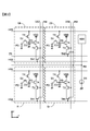
- FIG. 3 shows four pixels 30 (two in the vertical direction and two in the horizontal direction) in an area PB surrounded by a two-dot chain line at the lower right in the pixel block BC2 shown in FIG. 2B.
- FIG. 2 is a diagram showing an outline of an electric circuit of the first embodiment. As shown in the area PB of FIG. 2B, the four pixels 30 are a G pixel Gb at the upper left, a special pixel Z2 at the upper right, an R pixel R at the lower left, and a G pixel Gr at the lower right.
- Each of the four pixels is basically a four-transistor CMOS image sensor, but as will be described later, a so-called select transistor has a normal four-transistor CMOS image sensor. It is different from an image sensor.
- the photodiode PD which is a photoelectric conversion unit, photoelectrically converts incident light to generate charges, and temporarily stores the generated charges.
- the transfer transistor TX transfers the charge accumulated in the photodiode PD to a floating diffusion (FD) region FD in which a capacitor CC is formed, based on a transfer signal sent from a transfer control line (not shown) to a gate of the transfer transistor TX. .
- the amplification transistor TA outputs a signal corresponding to the charge generated by the photodiode PD when a voltage generated in the FD region FD due to the transferred charge is applied to its gate.
- the power supply voltage VDD is applied to the input side (drain) of the amplification transistor TA.
- a reset transistor TR for resetting the FD region FD to a predetermined voltage is provided.
- the input side (drain) of the reset transistor TR is connected to the reset voltage line HR3 or HR4, and a predetermined voltage described later is supplied from the horizontal control unit HC via the reset voltage line HR.
- the output side (source side) of the amplification transistor TA of each pixel (Gb, Z2, R, Gr) is connected to the input side of the vertical selection transistor TV.
- a vertical selection line VS7 or VS8 is connected to the gate of the vertical selection transistor TV, and the vertical selection transistor TV is turned on or off by a control signal sent from the vertical control unit VC shown in FIG. It is controlled to be conductive.
- the output side of the vertical selection transistor TV of the imaging pixel (Gb, R, Gr) is connected to the input side of the horizontal selection transistor TH1. That is, the vertical selection transistor TV and the horizontal selection transistor TH1 are arranged in series.
- the gate of the horizontal selection transistor TH1 is connected to a horizontal selection line HS3 or HS4, and the horizontal selection transistor TH1 is turned on or off by a control signal sent from the horizontal control unit HC shown in FIG.
- the amplification transistor TA, the vertical selection transistor TV, and the horizontal selection transistor TH1 can be interpreted as an integrated unit or any of them as an output unit. .
- the output side of the vertical selection transistor TV is connected to the input side of the special horizontal selection transistor TH2.
- the gate of the special horizontal selection transistor TH2 is connected to the special horizontal selection line ZS, and the special horizontal selection transistor TH2 is turned on or off by a control signal sent from the horizontal control unit HC shown in FIG. It becomes conductive.
- the amplification transistor TA, the vertical selection transistor TV, and the special horizontal selection transistor TH2 of the special pixel Z2 of the image sensor 3 according to the embodiment can be interpreted as an output unit, or one of them.
- the output section of the horizontal selection transistor TH1 of the imaging pixel (Gb, R, Gr) in the pixel block BC2 and the output section of the special horizontal selection transistor TH2 in the special pixel Z2 in the pixel block BC2 are all one output line. Connected to RW. Further, the output line RW is connected to a reading unit that reads out a signal of the pixel 30.
- the readout unit includes, for example, an AD conversion unit ADC that converts an analog signal output from the pixel 30 into a digital signal.
- the output line RW is connected to a current source CS that supplies a current to each pixel 30.
- the control unit CU controls the voltage of the control signal to the vertical selection line VS and the horizontal selection line HS, thereby controlling the signal (Gb, Z2, R, Gr) of one or more pixels (Gb, Z2, R, Gr) in the pixel block BC2.
- the output of the amplification transistor TA) is output to the output line RW.
- the reading unit reads a signal of a pixel (Gb, Z2, R, Gr) in the pixel block BC2.
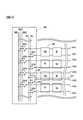
- FIG. 4 is a circuit diagram included in the horizontal control unit HC.
- FIG. 4 illustrates a part of the circuit included in the horizontal control unit HC, a part of the plurality of pixels 30, and a part of the horizontal selection line HS connected to the pixels 30 in the above-described pixel blocks BC1 and BC2. Part of the special horizontal selection line ZS and the reset voltage line HR are shown.
- Each horizontal selection line HS is connected to selection line changeover switches SS1 to SS4 (also collectively referred to as selection line changeover switch SS) in the horizontal control section HC.
- selection line switch SS By the selection line switch SS, each horizontal selection line HS is connected to a high voltage line SH supplied with a high voltage such as a power supply voltage VDD or a low voltage line supplied with a low voltage such as a ground voltage GND. It is connected to any of the SLs in a switchable manner.
- the horizontal selection transistor TH1 in the pixel 30 to which the horizontal selection line HS1 is connected becomes conductive.
- the horizontal selection transistor TH1 is turned off.
- the special horizontal selection line ZS is connected to the special changeover switch SZ in the horizontal control unit HC.
- the special horizontal selection line ZS is switchably connected to either the high voltage line SH or the low voltage line SL by the special changeover switch SZ.
- the special horizontal selection line ZS is connected to the high voltage line SH, the horizontal selection transistor TH2 in the pixel 30 to which the special horizontal selection line ZS is connected becomes conductive.
- the horizontal selection transistor TH2 is turned off.
- each reset voltage line HR is connected to reset line changeover switches SR1 to SR4 (generically referred to as reset line changeover switch SR) in the horizontal control section HC.
- Each reset voltage line HR is supplied with a first voltage line RR1 to which a first voltage such as a power supply voltage VDD is supplied, and a second voltage closer to the substrate voltage than the first voltage is supplied to each reset voltage line HR by the reset line changeover switch SR.
- a third voltage line RR3 to which a third voltage closer to the substrate voltage than the second voltage is supplied.
- the horizontal control unit HC applies one of the first voltage, the second voltage, and the third voltage to the input side of the reset transistor TR in each pixel 30 via a reset voltage line HR.
- Each of the selection line changeover switch SS, the special changeover switch SZ, and the reset line changeover switch SR can be configured by a semiconductor switch, for example, a MOS transistor circuit.
- a changeover switch for switching the voltage applied to each vertical selection line VS is also arranged in the vertical control unit VC, similarly to the horizontal control unit HC shown in FIG. Switching of these switches, that is, what voltage signals are sent to each of the vertical selection line VS, the horizontal selection line HS, the special horizontal selection line ZS, and the reset voltage line HR is determined by a control circuit in the control unit CU. Can be controlled by Note that the control unit CU can also control the movement of the changeover switch based on instructions from various devices and devices on which the image sensor is mounted.
- the gate of the transfer transistor TX and the gate of the reset transistor TR in each pixel 30 shown in FIG. 3 are connected to the horizontal selection line HS or the vertical selection line VS similarly to the conventional CMOS image sensor.
- a similar control line (not shown) is connected.
- the control unit CU can control the conduction state of the transfer transistor TX and the reset transistor TR for each pixel 30 arranged in one row in the x direction or one column in the y direction by the control line.
- each of the control lines is also constituted by two control lines in the horizontal and vertical directions, and each of the transfer transistor TX and the reset transistor TR is constituted by two transistors arranged in series. . Then, one of a horizontal control line and a vertical control line may be connected to each of the gates of the two transistors.
- signals of an arbitrary number of pixels 30 in one pixel block BC connected to one readout unit are output via the output line RW and the readout unit.
- Summing and reading are possible.
- the imaging device 3 can be easily applied to, for example, use in a low resolution mode in which image data having a smaller number of pixels than the total number of pixels of the imaging device is output.
- noise mixed into the signal of each pixel 30 is smoothed by adding and reading out two or more pixels 30 in one pixel block BC by a readout unit. Obtainable.
- the plurality of pixels 30 added at the time of reading by the reading unit be pixels of the same color. Therefore, the vertical control unit VC and the horizontal control unit HC control the voltage of the control signal to the vertical selection line VS and the horizontal selection line HS to select two or more pixels 30 of the same color in one pixel block BC. Then, those signals (output of the amplification transistor TA) are output to the output line RW.
- the clip operation pixel functions as a pixel that only outputs a fixed signal for clipping, and need not be a pixel of the same color as the readout pixel.
- the readout pixel is a G pixel (imaging pixel) Gb arranged at the upper left in FIG. 3
- the clipping pixel is an R pixel (imaging pixel) R arranged at the lower left in FIG. It will be described as. However, as will be described later, another arbitrary pixel 30 may be selected as the read pixel and the clip operation pixel.
- the control unit CU including the horizontal control unit HC controls the reset line changeover switch SR so that each reset voltage line HR is supplied with the first voltage supplied with the first voltage. Connect to voltage line RR1. Then, the control unit CU turns on the reset transistor TR and the transfer transistor TX of each pixel 30 to reset the FD region and the photodiode PD to the above-described first voltage.
- control unit CU turns off the transfer transistor TX, and performs exposure for imaging or focus detection on the photodiode PD on the image sensor 3.
- a signal based on the charge generated in the photodiode PD by the exposure is read out using so-called correlated double sampling.
- the control unit CU applies a high-level voltage to the horizontal selection line HS3, the horizontal selection line HS4, and the vertical selection line VS7, and controls the vertical selection transistor TV and the horizontal selection transistor TH1 of the read pixel Gb and the clip operation pixel R, respectively. Conducted state.
- the outputs of the respective amplification transistors TA of the read pixel Gb and the clipping pixel R are output to the output line RW and are added.
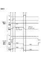
- the horizontal axis represents time
- TX and TR represent voltages of control signals input to the gates of the transfer transistor TX and the reset transistor TR of each pixel 30.
- the control signal is at a high level (for example, power supply voltage)
- the transistor to which the control signal is input becomes conductive, and the control signal becomes low.
- the level for example, the ground voltage
- the transistor to which the control signal is input is turned off. 5
- the HR voltage indicates a voltage supplied to the reset voltage line HR connected to each pixel 30, and the FD voltage indicates a voltage in the FD region of each pixel 30.
- the control unit CU supplies a low-level control signal to the gates of any of the transfer transistor TX and the reset transistor TR of the read pixel Gb and the clipping pixel R. Then, the control unit CU supplies the first voltage VC1 to the reset voltage line HR of the read pixel Gb and the clip operation pixel R.
- the FD region FD of the read pixel Gb and the clip operation pixel R has been reset to the first voltage in the above-described reset operation.
- the voltage of the FD region FD at time t0 is uncertain due to the influence of noise or the like. is there.
- the control unit CU applies a high-level voltage to the gate of the reset transistor TR of the read pixel Gb from time t1 to time t2, and resets the FD region FD of the read pixel Gb to the first voltage VC1.
- the first voltage VC1 is applied to the gate of the amplification transistor TA in the read pixel Gb, and the amplification transistor TA generates an amplified signal based on the first voltage VC1, that is, a so-called dark signal in which the charge accumulated in the photodiode PD is not reflected.
- Output This output is output to the output line RW via the vertical selection transistor TV and the horizontal selection transistor TH1.
- the control unit CU applies a high-level signal to the gate of the reset transistor TR after time t1, and applies the second voltage to the reset voltage line HR connected to the clipping pixel R.
- Supply VC2 As a result, the FD area FD of the clip operation pixel R is reset to the second voltage VC2. Therefore, the second voltage VC2 is applied to the gate of the amplification transistor TA in the clip operation pixel R, and the amplification transistor TA outputs an amplified signal based on the second voltage VC2. This output is output to the output line RW via the vertical selection transistor TV and the horizontal selection transistor TH1.
- the signal of the read pixel Gb and the signal of the clipping pixel R are added as so-called source binning. Therefore, the voltage of the signal finally read from the reading unit substantially matches the higher voltage of the voltage signals when both signals before summing are read separately from the reading unit. Therefore, the second voltage VC2 applied to the reset transistor TR of the clipping pixel R is set as follows. That is, the output voltage value of the read unit when only the clipping pixel R is connected does not exceed the assumed output voltage value of the read unit when only the read pixel Gr that outputs the dark signal is connected. The second voltage VC2 is set to have a value.
- the second voltage VC2 is set to a voltage lower (closer to the ground voltage) than the first voltage VC1.
- the control unit CU instructs the reading unit to read a signal. In this state, the voltage applied to the input unit of the reading unit is AD-converted, and dark sampling is performed.
- control unit CU applies a high-level voltage to the gate of the transfer transistor TX of the readout pixel Gb from the time t3 to the time t4, and causes the charges in the photodiode PD generated by the photoelectric conversion to be in the FD region.
- the voltage supplied to the reset voltage line HR connected to the clipping pixel R is changed to the third voltage VC3.
- the FD area FD of the clip operation pixel R is reset to the third voltage VC3.
- the control unit CU instructs the reading unit to read a signal.
- the voltage applied to the input unit of the reading unit is AD-converted, and signal sampling is performed.
- the third voltage VC3 is also set as follows. That is, the third voltage VC3 is set so that the output voltage value of the readout unit to which only the clipping pixel R is connected does not exceed the assumed value of the output voltage of the readout unit to which only the readout pixel Gr is connected. Is set.
- the third voltage VC3 is preferably lower than the second voltage VC2, and may be a voltage that is about 30 to 70% of the second voltage VC2 based on the ground voltage.
- the amplifying transistor TA in each pixel 30 is a pMOS type, the relationship between the first voltage, the second voltage, and the third voltage is reversed.
- the reading unit calculates a difference between the result of the signal sampling and the result of the dark sampling, and outputs the difference as a result of reading the light amount signal from the read pixel Gb. Therefore, the read signal by dark sampling can be interpreted as a correction signal for correcting the read signal by signal sampling.
- the output read by the reading unit in each pixel block BC is output from the image sensor 3 via an output control circuit (not shown).
- the control unit CU supplies a high-level voltage for turning on the vertical selection transistor TV to the vertical selection lines VS5 and VS7 connected to the four G pixels Gb and the two R pixels R, and supplies these pixels. Is supplied to the horizontal selection lines HS1, HS3 and HS4 connected to the horizontal selection transistor TH1.
- a low-level voltage is supplied to the horizontal selection line HS2, special horizontal selection line ZS, and vertical selection lines VS6 and VS8 that are not connected to these pixels.
- the pixels 30 in each pixel block BC2 only the signals from the four G pixels Gb that are readout pixels and the two R pixels R connected to the horizontal selection line HS4 are connected to the output line RW, It can be read by the reading unit.
- the reading may be performed by using the four G pixels Gb as the read pixels and the two R pixels R connected to the horizontal selection line HS4 as the clip operation pixels.
- the first voltage VC1 is always applied to the reset voltage lines HR1 and HR3 connected to the reset units of the four G pixels Gb, and the reset transistor TR and the transfer transistor TX are shown in FIG.
- a high-level voltage is applied at a predetermined timing (predetermined timing of a read pixel).
- the reset voltage line HR4 connected to the reset units of the two R pixels R connected to the horizontal selection line HS4 has the first voltage VC1 at the predetermined timing (the predetermined timing of the clip operation pixel) shown in FIG.
- the second voltage VC2 and the third voltage VC3 are sequentially applied.
- a high-level voltage is applied to the reset transistors TR of the two R pixels R connected to the horizontal selection line HS4 at a predetermined timing.
- the read pixel and the clip operation pixel can be selected from pixels of the same color.
- a high-level voltage is applied only to the vertical selection line VS5
- a low-level voltage is applied to the other vertical selection lines VS
- a high-level voltage is applied to the horizontal selection lines HS1 and HS3.
- a low-level voltage is applied to the horizontal selection lines HS2 and HS4.
- only the signals of the two G pixels Gb connected to the vertical selection line VS5 can be connected to the output line RW.
- the horizontal control unit HC supplies a signal supplied to the reset voltage line HR and the horizontal selection line HS as follows. Control the level.
- the first voltage VC1 is always supplied to the reset voltage line HR1 according to the timing chart of FIG.
- the first voltage VC1, the second voltage VC2, and the third voltage VC3 are sequentially supplied to the reset voltage line HR3 according to the timing, and the gates of the reset transistor TR and the transfer transistor TX are appropriately set to a high level according to the timing. Supply level voltage.
- reading can be performed using the G pixel Gb connected to the reset voltage line HR1 as a read pixel and the G pixel Gb connected to the reset voltage line HR3 as a clip operation pixel.
- the G pixel Gb is the readout pixel
- the G pixel Gr, the R pixel R, the B pixel B, or the special pixel ZZ can be similarly used as the readout pixel.
- the clip operation pixel a pixel of the same color as the readout pixel can be used, or a pixel of a different color from the readout pixel can be used.
- a special horizontal pixel connected to the special pixel ZZ is used instead of the horizontal selection line HS in order to output a signal of the special pixel ZZ to the output line RW.
- a high-level voltage is applied to the selection line ZS.
- a part of the B pixel B having high sensitivity to blue light is replaced by the special pixels Z1 and Z2, but the read operation from the B pixel B in the pixel block BC2 is performed. Can be performed in substantially the same manner as the above-described read operation from the G pixel Gr.
- a horizontal selection line HS1 a special horizontal selection line ZS
- a vertical selection line VS6 a vertical selection line A high-level voltage is applied to the line VS8. Then, a low-level voltage is applied to the other horizontal selection lines HS and vertical selection lines VS.
- a high-level voltage is applied to the horizontal selection line HS2 instead of the special horizontal selection line ZS, and a predetermined voltage is applied to the reset voltage line HR2 in accordance with the timing shown in FIG.
- Two G pixels Gr connected to the horizontal selection line HS2 can be used as clip operation pixels.
- the horizontal selection line HS3 arranged in parallel with the special horizontal selection line ZS is not connected to the special horizontal selection transistor TH2 in the special pixels Z1 and Z2. Therefore, when reading the signal of the B pixel B in the pixel block BC2, regardless of what signal the horizontal control unit HC sends to the horizontal selection line HS3, the signal read from the B pixel B includes the special pixels Z1 and Z2. No signal is mixed. However, since the horizontal selection line HS3 is shared by the other pixel blocks BC such as the pixel block BC1 adjacent to the pixel block BC2 in the x direction, the signal applied to the horizontal selection line HS3 is not used by the other pixel blocks BC. It is preferable to add a signal suitable for reading the data.
- the signal of the special pixel ZZ can be read by using the special pixel ZZ as a read pixel and the other imaging pixel 30c as a clip operation pixel.
- the special pixel Z2 in the region PB is read out as a pixel to be read and the G pixel Gr in the region PB is read out as a clip operation pixel
- a high level is applied to the vertical selection line VS8, horizontal selection line HS4, and special horizontal selection line ZS. Apply voltage.
- a low-level voltage is applied to the other vertical selection lines VS and horizontal selection lines HS.
- the signal of the special pixel Z2 in the area PB and the signal of the G pixel Gr in the area PB can be connected to the output line RW. Then, similarly to the above example, a predetermined voltage is applied to the reset voltage line HR or the like so that the special pixel Z2 in the region PB becomes a read pixel and the G pixel Gr in the region PB becomes a clip operation pixel. What is necessary is just to perform the correlation double sampling mentioned above.
- a signal of each pixel 30 in each pixel block BC is output to an output line RW provided in each pixel block BC, and is read by a reading unit.
- the vertical selection line VS, the horizontal selection line HS, and the special horizontal selection line ZS may be shared by a plurality of pixel blocks BC even when reading out pixel blocks other than the pixel block BC2.
- the horizontal selection lines HS1 to HS4 may be connected to each pixel 30 of another pixel block BC arranged in the x direction with respect to the pixel block BC2, like the pixel block BC1.
- the vertical selection lines VS5 to VS8 may be connected to each pixel 30 of another pixel block BC arranged in the y direction with respect to the pixel block BC2.
- the order of reading the signals of the special pixel ZZ and the imaging pixels (Gb, Gr, R, B) is arbitrary.
- the control unit CU first selects the special pixel ZZ via the vertical selection line VS and the horizontal selection line HS, the reading unit reads the output signal, and thereafter, the imaging pixels (Gb, Gr, R, B). ), And the reading unit reads the output signal.
- the signal of the special pixel ZZ is used. Is shorter than the time required to read the signals of the imaging pixels. That is, the reading of the signal of the special pixel ZZ can be performed faster than the reading of the signal of the imaging pixel 30c.
- the control unit 4 focuses by reading the signal of the special pixel ZZ before reading the signal of the imaging pixels (Gb, Gr, R, B). Detection can be performed at high speed.
- two readout units may be provided in one pixel block BC. By connecting two readout units to one output line RW, each of the two readout units may read out the signal of the special pixel ZZ and the signal of the imaging pixel (Gb, Gr, R, B).
- the reading unit can read the signal of the special pixel ZZ and the signal of the imaging pixel (Gb, Gr, R, B) under conditions such as the optimum reading gain.
- a high-level signal (transfer signal) is not applied to the gate of the transfer transistor TX in the clip operation pixel. Therefore, the charge (photoelectric signal) generated by the exposure is stored in the photodiode PD in the pixel used as the clip operation pixel. Therefore, after the reading by the combination of the reading pixel and the clipping pixel described above is completed, at least one of the pixels used as the clipping pixel can be set as the reading pixel and the signal can be read.
- the voltage applied to the reset portion (reset transistor TR) of the clip operation pixel may be the first voltage VC1 or the second voltage VC2.
- the voltage source connected to the reset voltage line HR by the reset line changeover switch SR in the horizontal control unit HC is the first voltage line RR1, the second voltage closer to the substrate voltage than the first voltage.
- the number of the supplied second voltage lines RR2 may be two.
- the HR voltage (the voltage supplied to the reset voltage line HR connected to the clipping pixel) in the case of the clipping pixel shown in FIG. 5 is the first voltage VC1 from time t0 to time t1, and After t1, the second voltage VC2 may be used. In this case, the second voltage VC2 may be about 20 to 40% of the first voltage VC1 based on the ground voltage.
- the read pixel can be interpreted as the first pixel.
- a clip operation pixel can be interpreted as a second pixel.
- the charge photoelectrically converted by the photodiode PD is transferred and stored therein, and thus can be interpreted as a storage unit.
- the FD region FD of the readout pixel first pixel
- the FD region FD of the clipping pixel second pixel
- the pixels 30 that are added and read by source binning may be a plurality of read pixels only, without using the clip operation pixels. This can be realized by not selecting a pixel used as a clip operation pixel in the above-described readout example. Specifically, at the time of correlated double sampling, the clip operation pixel is not selected by the vertical selection line VS, the horizontal selection line HS, and the special horizontal selection line ZS, or various reset voltages are applied to the clip operation pixel at a predetermined timing. Alternatively, a signal for controlling the reset transistor TR may not be sent.
- any one or more of the plurality of pixels 30 read out in total can be interpreted as the first pixel, and one or more of the pixels other than the first pixel can be interpreted as the second pixel.
- the voltage generated in the FD region FD of the first pixel to which the charge generated by the photodiode PD has been transferred is the first voltage
- the voltage generated in the FD region FD of the second pixel to which the charge generated by the photodiode PD has been transferred is a first voltage. It can also be interpreted as the second voltage.
- FIG. 6 is a diagram showing a cross section of a pixel 30 portion of the image sensor 3 of the present embodiment.
- FIG. 6 shows only a part of the cross section of the entire image sensor 3.
- the z direction and the z direction shown in FIG. 6 are the same as the respective directions shown in FIG.
- the image sensor 3 is a so-called back-illuminated image sensor.
- the image sensor 3 photoelectrically converts light incident from above on the paper.
- the imaging device 3 includes a first semiconductor substrate 7 and a second semiconductor substrate 8.
- the image sensor 3 has the plurality of pixels 30.
- One pixel 30 includes a pixel upper portion 30 x provided on the first semiconductor substrate 7 and a pixel lower portion 30 y provided on the second semiconductor substrate 8.
- One pixel upper part 30x includes one micro lens 74, one color filter 73, the light receiving part 31 of one photodiode PD, and the like.
- the first semiconductor substrate 7 includes a light receiving layer 71 including the light receiving portion 31 of the photodiode PD included in the pixel upper part 30x, and a wiring layer 72 on which transistors such as the transfer transistor TX and the amplification transistor TA are formed.
- the light receiving layer 71 is arranged on the opposite side (back side) of the first semiconductor substrate 7 from the wiring layer 72.
- a plurality of light receiving sections 31 are two-dimensionally arranged. Since the pixel upper part 30x includes the light receiving part 31 which is a part for photoelectrically converting incident light, it can be interpreted as an imaging part.
- a vertical selection transistor TV On the second semiconductor substrate 8, a vertical selection transistor TV, a horizontal selection transistor TH1, a special horizontal selection transistor TH2, a vertical selection line VS, a horizontal selection line HS, a special horizontal selection line ZS included in the pixel lower portion 30y, A current source CS and the like are arranged.
- a plurality of bumps 75 are arranged on the surface of the wiring layer 72.
- a plurality of bumps 76 corresponding to the plurality of bumps 75 are arranged.
- the plurality of bumps 75 and the plurality of bumps 76 are joined to each other.
- the first semiconductor substrate 7 and the second semiconductor substrate 8 are electrically connected via the plurality of bumps 75 and the plurality of bumps 76, that is, the first semiconductor substrate 7 and the second semiconductor substrate 8 are stacked. Have been. Note that since the reading unit that reads signals from the plurality of pixels 30 is provided on the second semiconductor substrate 8, it can be interpreted that the reading unit is stacked on the imaging unit provided on the first semiconductor substrate 7. .
- the configuration of the circuit elements arranged on the first semiconductor substrate 7 and the second semiconductor substrate 8 described above is merely an example, and some of the components are the first semiconductor substrate 7 and the second semiconductor substrate 8. May be arranged in either of them.
- the special horizontal selection line ZS may be formed on the first semiconductor substrate 7, and the read section and the current source CS may be arranged on the second semiconductor substrate 8.
- the vertical control unit VC and the horizontal control unit HC may be arranged on either the first semiconductor substrate 7 or the second semiconductor substrate 8. However, if a large number of circuit elements are arranged on the first semiconductor substrate 7, the area or volume for disposing the light receiving unit 31 on the first semiconductor substrate 7 cannot be sufficiently secured. Preferably, it is arranged on the substrate 8.
- the color filter 73 of each pixel 30 is provided with a color filter that matches the spectral sensitivity characteristics of each pixel. Further, the color filter 73 is also arranged in the special pixel ZZ of the pixels 30. When the special pixel ZZ is an AF pixel, a G color filter is provided as the color filter 73. Note that the color filter 73 provided in the special pixel ZZ may be a filter that transmits the entire wavelength range of the incident light. Further, the color filter 73 provided in the special pixel ZZ may be a color filter 73 having a different spectral characteristic from any of the color filters 73 provided in the imaging pixel 30c.
- the color filter 73 When the special pixel ZZ is a pixel for receiving infrared light, the color filter 73 has a high infrared light transmittance and a low visible light transmittance. When the special pixel ZZ is a pixel for receiving visible light, the color filter 73 has a high transmittance over the entire visible light wavelength range.
- the sensitivity of the special pixel ZZ may be made different from the sensitivity of the imaging pixel 30c by making the average transmittance of the color filter 73 of the special pixel ZZ different from the average transmittance of the color filter 73 of the imaging pixel 30c.
- the average transmittance refers to the average of the transmittance of all the wavelengths of light that is photoelectrically converted by the light receiving unit 31.
- the sensitivity of the special pixel ZZ is determined by making the area of the light receiving section 31 of the special pixel ZZ different from the area of the light receiving section 31 of the imaging pixel 30c or changing the condition of ion implantation into the light receiving section 31. The sensitivity may be different.
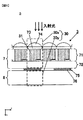
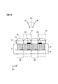
- FIG. 7 is a diagram illustrating an example where the special pixel ZZ is an AF pixel.
- the second semiconductor substrate 8 is omitted from the cross-sectional view of the imaging device 3 shown in FIG.
- the special pixel Z ⁇ b> 1 is provided with a light shielding unit 75 ⁇ / b> R that shields the right side of the light receiving unit 31 at the boundary between the color filter 73 and the first semiconductor substrate 7.
- the special pixel Z2 is provided with a light shielding portion 75L that shields the left side of the light receiving portion 31 from light at the boundary.
- the special pixel Z1 Of the light incident on the special pixel Z1, the light LL that is incident in the ⁇ x direction with respect to the direction PL perpendicular to the incident surface of the imaging element 3 is shielded by the light shielding unit 75R.
- the light LR incident obliquely in the + x direction with respect to the direction PL perpendicular to the incident surface of the imaging element 3 is shielded by the light shielding portion 75L.
- the special pixels Z1 and Z2 have reduced sensitivity to light incident from different incident directions, and conversely, have relatively higher sensitivity to light incident from different incident directions.
- the special pixels Z1 and Z2 are elements having high sensitivity to light passing through different positions on the pupil plane of the image pickup optical system 2, so that the image plane phase difference Functions as a pixel for focus detection.
- the positions at which the light shielding portions 75R and 75L are provided are not limited to the above-described boundary between the color filter 73 and the first semiconductor substrate 7, but are provided anywhere between the microlens 74 and the first semiconductor substrate 7. Just do it.
- the arrangement of the pixels 30 is not necessarily limited to the Bayer arrangement.
- the horizontal selection line HS and the special horizontal selection line ZS may extend not in the long side direction but in the short side direction of the image sensor 3, and the vertical selection line VS is not in the short side direction of the image sensor 3 but in the long side. It may extend in the direction.
- the horizontal selection line HS, the special horizontal selection line ZS, and the vertical selection line VS that control the output of the signal of each pixel 30 always extend in the horizontal direction (x direction) and the vertical direction (y direction). It is not necessary.
- the horizontal selection line HS, the special horizontal selection line ZS, and the vertical selection line VS may not be shared by the plurality of pixels 30.
- the special pixel ZZ may incorporate therein an amplifier circuit for increasing the signal output, for example, about twice.
- the value may be increased by adding an offset to the output signal from the special pixel ZZ.
- the total number of the imaging pixels 30c and the B pixels B in each pixel block BC varies depending on whether or not the pixel block BC includes the special pixel ZZ. Therefore, when performing the above-described binning reading, the magnitude of the addition signal of the pixel block BC may also vary depending on whether or not the pixel block BC includes the special pixel ZZ.
- a correction circuit for increasing or decreasing the addition signal of the pixel block BC including the special pixel ZZ according to the number of the special pixels ZZ included in the pixel block BC may be provided.
- This correction circuit may be provided in the pixel block BC, or may be provided in the imaging device 3 other than the pixel block BC. Alternatively, this correction may be performed by the control unit 4 instead of providing a correction circuit in the image sensor 3.
- the pixel block BC1 does not include the special pixel ZZ, but includes four G pixels Gb, G pixels Gr, B pixels B, and R pixels R each.
- the pixel block BC2 includes two special pixels ZZ (Z1, Z2), and includes four G pixels Gb, G pixels Gr, and R pixels R, but two B pixels B. Only included. Therefore, when performing binning reading of the B pixel B in the pixel block BC2, the addition signal is multiplied by (4/2). This makes it possible to make the addition signal at the time of binning readout of the B pixel B substantially equal between the pixel block BC1 and the pixel block BC2.
- the image sensor 3 of the above embodiment has a first pixel and a second pixel.
- the first pixel includes a photodiode (first photoelectric conversion unit) PD that photoelectrically converts light to generate a charge, an FD region (first storage unit) FD that stores charge generated by the photodiode PD, and
- the second pixel includes a selection transistor (first output unit) TH1 that outputs a first signal based on the voltage of the FD region FD, and the second pixel photoelectrically converts light to generate a charge (second photoelectric conversion unit).
- the image pickup device 3 of the above embodiment further includes an output line RW to which the selection transistor TH1 of the first pixel and the selection transistor TH1 or TH2 of the second pixel are connected, and the first signal and the second signal are output.
- a control unit CU that controls the voltage of the FD region FD of the first pixel to a first voltage, and controls the voltage of the FD region FD of the second pixel to a second voltage or a first voltage different from the first voltage. I have. With such a configuration, the output of any one or a plurality of pixels 30 can be selected from the plurality of pixels connected to the output line RW and output to the output line RW. doing.
- control unit CU can control the second storage unit to the second voltage while the first output unit outputs the first signal. Accordingly, even when the first signal has an abnormal value exceeding a predetermined range, it is possible to prevent an excessive current from being generated in the current source IS, and to prevent damage to the image sensor 3.
Landscapes
- Engineering & Computer Science (AREA)
- Multimedia (AREA)
- Signal Processing (AREA)
- Transforming Light Signals Into Electric Signals (AREA)
- Solid State Image Pick-Up Elements (AREA)
Abstract
Description
本発明の第2の態様によると、撮像装置は、第1の態様による撮像素子と、前記第1信号に基づいて画像データを生成する生成部と、を備える。
図1は、第1の実施の形態に係る撮像素子を用いた撮像装置の構成を模式的に示す断面図である。撮像装置1は、撮像光学系2、撮像素子3、制御部4、レンズ移動部5、および表示部6を備える。
図2(a)は、本発明の実施形態の撮像素子3を撮像面側から、すなわち図1の-Z側から見た図である。撮像素子3は、図2のx方向およびy方向に配列される複数の画素30を有している。図2では一部を省略して描いているが、画素30は、x方向およびy方向にそれぞれ例えば1000個以上に渡って多数配列されていてもよい。
複数の画素30が配列された領域(撮像領域)の、図中の左端には水平制御部HCが設けられ、図中の上端には垂直制御部VCが設けられている。水平制御部HCと垂直制御部VCを合わせて、制御部CUとも呼ぶ。
撮像素子3は、複数の画素ブロックBCを有する。図2では、1つの画素ブロックBCは、破線で示した境界線BBにより囲まれる領域に、x方向およびy方向に配列された複数の画素30を有する。境界線BBで囲まれた領域は1つの画素ブロックBCを構成する。各画素ブロックBCのそれぞれの中の複数の画素30は、後述するようにそれぞれの出力部が1つの出力線に接続され、各画素30が1つの読出部に接続されている。なお、画素ブロックBCのそれぞれの中の複数の画素30は、複数の出力線に接続され、複数の読出部に接続されていてもよい。
図2では、説明を容易にするために1つの画素ブロックBCに相当する部分にハッチング付している。ただし、破線で示した各境界線BBにより囲まれる各領域がそれぞれ画素ブロックBCである。複数の画素30は分割されて、複数の画素ブロックBCの中に配列されている。
また、画素ブロックBCの外郭形状は図2に示した長方形に限られるものではなく、複数の画素30を包含する任意の形状であってもよい。この場合、境界線BBの形状は単純な直線ではなく、複数の直線が折れ曲がって接続された形状になる。
特殊画素ZZは、AF画素に限らず、感度が上述の撮像画素30cのいずれとも異なる画素であってもよい。また、分光特性が上述の撮像画素30cのいずれとも異なるカラーフィルタを有する画素であってもよい。
複数の画素ブロックBCのうち少なくとも1つの画素ブロックBCは、画素ブロックBC2のように少なくとも1つの特殊画素ZZと複数の撮像画素30cで構成される。撮像素子3の複数の画素ブロックBCが全て特殊画素ZZを含む画素ブロックBC2で構成されていてもよい。撮像素子3の複数の画素ブロックBCのうち少なくとも一つが特殊画素ZZを含む画素ブロックBC2、他の画素ブロックBCが全て撮像画素30cで構成される画素ブロックBCであってもよい。
水平制御部HCからは、各画素30の後述するリセット部に接続されているリセット電圧線HR1~HR4(総称して、リセット電圧線HRとも呼ぶ)がx方向に延びている。
4つの画素(Gb,Z2,R,Gr)は、いずれも基本的には4トランジスタ型のCMOS型撮像素子であるが、後述するとおり、いわゆる選択トランジスタの構成が通常の4トランジスタ型のCMOS型撮像素子とは異なっている。
実施形態の撮像素子3の撮像画素(Gb,R,Gr)において、増幅トランジスタTA、垂直選択トランジスタTV、および水平選択トランジスタTH1を一体として、あるいはそのいずれかを、出力部と解釈することができる。
実施形態の撮像素子3の特殊画素Z2の増幅トランジスタTA、垂直選択トランジスタTV、および特殊水平選択トランジスタTH2を一体として、あるいはそのいずれかを、出力部と解釈することができる。
特殊水平選択線ZSは、水平制御部HCにおいて特殊切替スイッチSZに接続されている。特殊切替スイッチSZにより、特殊水平選択線ZSは、高電圧線SHか低電圧線SLかのいずれかに、切替可能に接続される。例えば、特殊水平選択線ZSが、高電圧線SHに接続された場合、特殊水平選択線ZSが接続される画素30内の水平選択トランジスタTH2は導通状態となる。特殊水平選択線ZSが、低電圧線SLに接続された場合、その水平選択トランジスタTH2は非導通状態となる。
選択線切替スイッチSS、特殊切替スイッチSZ、リセット線切替スイッチSRは、いずれも、半導体スイッチ、たとえばMOSトランジスタ回路で構成することができる。
これらの各スイッチの切替え、すなわち垂直選択線VS、水平選択線HS、特殊水平選択線ZS、およびリセット電圧線HRのそれぞれにどのような電圧の信号を送るかは、制御部CU内の制御回路により制御することができる。
なお、制御部CUは、撮像素子が実装される各種装置、機器からの指示に基づき切替スイッチを移動制御することもできる。
ビニング読出しにより、撮像素子3を、例えば撮像素子の総画素数よりも少ない画素数の画像データを出力する低解像度モードでの使用に、容易に適用することができる。ビニング読出しでは、1つの画素ブロックBC内の2つ以上の画素30を、読出部により合算して読み出すことにより各画素30の信号に混入するノイズが平滑化されるため、よりノイズの少ない画像を得ることができる。
信号を読み出す際に、読出部の入力側における信号の電圧が所定の値を下回った場合のように読出部に異常値が出力される場合、画素ブロックBC内の出力線RWに繋がる電流源CSや読出部に過剰な電流が流れる等により、電流源CSや読出部が損傷する恐れがある。
これを防止するために、本実施形態の撮像素子3では、以下のようにして過剰な電流を抑制することができる。すなわち、1つの画素ブロックBC内の任意の1つ以上の読出し画素の読み出し時に、1つの画素ブロックBC内の他の任意の画素30をクリップ動作画素とし、読出し画素とクリップ動作画素の信号を合算して読み出すことにより、過剰な電流を抑制することができる。
クリップ動作画素は、クリップのための一定の信号を出力するだけの画素として機能するで、読出し画素と同色の画素である必要はない。
露光後に、露光によりフォトダイオードPDに生じた電荷に基づく信号を、いわゆる相関二重サンプリングを用いて読み出す。制御部CUは、水平選択線HS3、水平選択線HS4、および垂直選択線VS7にハイレベルの電圧を印加し、読出し画素Gbとクリップ動作画素Rのそれぞれの垂直選択トランジスタTVおよび水平選択トランジスタTH1を導通状態とする。これにより、読出し画素Gbとクリップ動作画素Rのそれぞれの増幅トランジスタTAの出力は、出力線RWに出力され、合算されることとなる。
図5に示すタイミングチャートにおいて、横軸は時刻を示しており、TXおよびTRは、各画素30の転送トランジスタTXおよびリセットトランジスタTRのゲートに入力される制御信号の電圧を示している。一例として、各画素30内の各トランジスタをnMOS型としているので、図5において、制御信号がハイレベル(例えば電源電圧)の場合に制御信号が入力されるトランジスタが導通状態となり、制御信号がローレベル(例えば接地電圧)の場合に制御信号が入力されるトランジスタが非導通状態となる。
図5の、HR電圧は、各画素30に接続されるリセット電圧線HRに供給される電圧を示し、FD電圧は、各画素30のFD領域の電圧を示している。
なお、読出し画素Gbおよびクリップ動作画素RのFD領域FDは、前述のリセット動作において第1電圧にリセットされているが、その後ノイズ等の影響により、時刻t0におけるFD領域FDの電圧は不確定である。
従って、クリップ動作画素RのリセットトランジスタTRに印加する第2電圧VC2は以下のように設定される。すなわち、仮にクリップ動作画素Rのみが接続されたときの読出部の出力電圧値が、仮にダーク信号を出力する読出し画素Grのみが接続されたときの読出部の出力電圧値の想定値を上回らない値となるように、第2電圧VC2は設定される。
制御部CUは、読出部に信号の読出しを指令し、この状態で読出部の入力部に加わる電圧がAD変換され、ダークサンプリングが行われる。
第3電圧VC3も以下のように設定される。すなわち、仮にクリップ動作画素Rのみが接続された読出部の出力電圧値が、仮に読出し画素Grのみが接続された読出部の出力電圧の想定値を上回らない値となるように、第3電圧VC3は設定される。
なお、各画素30内の増幅トランジスタTAがpMOS型である場合、上記の第1電圧、第2電圧、および第3電圧の高低関係は逆転する。
各画素ブロックBC内の読出部で読み出された出力は、不図示の出力制御回路を経て、撮像素子3から出力される。
次に、制御部CUが垂直選択線VS、水平選択線HS、および特殊水平選択線ZSの信号レベルを制御することにより行われる読出し画素およびクリップ動作画素の選択動作について、図2(b)および図3を参照して説明する。
この場合、制御部CUは、4つのG画素Gbおよび2つのR画素Rに接続されている垂直選択線VS5、VS7に、垂直選択トランジスタTVを導通させるハイレベルの電圧を供給し、これらの画素に接続されている水平選択線HS1、HS3、HS4に、水平選択トランジスタTH1を導通させるハイレベルの電圧を供給する。
これにより、各画素ブロックBC2内の画素30のうち、読出し画素である4つのG画素Gbと水平選択線HS4に接続される2つのR画素Rからの信号のみを、出力線RWに接続し、読出部により読み出すことができる。
具体的には、4つのG画素Gbのリセット部に接続されるリセット電圧線HR1、HR3には、常に第1電圧VC1を印加し、リセットトランジスタTRおよび転送トランジスタTXには、図5に示した所定のタイミング(読出し画素の所定のタイミング)でハイレベルの電圧を印加する。
これにより、画素ブロックBC2内において、2つのR画素Rをクリップ動作画素とし、4つのG画素Gbを読み出し画素として、ビニング読出しを行うことができる。
また、垂直選択線VS5にもローレベルの電圧を印加することで、画素ブロックBC2内の、水平選択線HS3と垂直選択線VS7に接続している1つのG画素Gbを読み出し画素とし、1つのR画素Rをクリップ動作画素として、ビニング読出しを行うこともできる。
例えば、画素ブロックBC2内で、垂直選択線VS5にのみハイレベルの電圧を印加し、他の垂直選択線VSにはローレベルの電圧を印加し、水平選択線HS1、HS3にハイレベルの電圧を印加し、水平選択線HS2、HS4にはローレベルの電圧を印加する。
これにより、垂直選択線VS5と接続されている2つのG画素Gbの信号のみを、出力線RWに接続することができる。これは、一方のG画素Gbを読出し画素、他方のG画素Gbをクリップ動作画素とする一例であり、水平制御部HCは、次のようにリセット電圧線HRおよび水平選択線HSに供給する信号レベルを制御する。
その場合、クリップ動作画素としても、同様に、読出し画素と同色の画素を使用することもでき、あるいは読出し画素と異なる色の画素を使用することもできる。
図2(b)に示す画素ブロックBC2においては、青色光に対して感度の高いB画素Bの一部が特殊画素Z1、Z2で置き換わっているが、画素ブロックBC2におけるB画素Bからの読み出し動作も、上述のG画素Grからの読み出し動作とほぼ同様に行うことができる。
ただし、水平選択線HS3は、画素ブロックBC2とx方向に隣接する画素ブロックBC1等の他の画素ブロックBCにおいても共用されているので、水平選択線HS3に加える信号は、他の画素ブロックBCでの読み出しに適した信号を加えることが好ましい。
一例として、領域PB内の特殊画素Z2を読出し画素、領域PB内のG画素Grをクリップ動作画素として読み出す場合は、垂直選択線VS8、水平選択線HS4、および特殊水平選択線ZSにハイレベルの電圧を印加する。そして、他の垂直選択線VSおよび水平選択線HSにはローレベルの電圧を印加する。
そして、以上の例と同様に、領域PB内の特殊画素Z2が読出し画素に、領域PB内のG画素Grがクリップ動作画素となるようにリセット電圧線HR等に所定の電圧を印加して、上述の相関2重サンプリングを行えばよい。
また、1つの画素ブロックBCに、2つの読出部を設けてもよい。1つの出力線RWに2つの読出部を接続させることで、2つの読出部それぞれが特殊画素ZZの信号と撮像画素(Gb、Gr、R、B)の信号とを読み出すようにしてもよい。これにより、読出部は、特殊画素ZZの信号と撮像画素(Gb、Gr、R、B)の信号とをそれぞれ最適の読出しゲイン等の条件で読み出すことができる。
従って、以上で説明した読出し画素とクリップ動作画素の組合せによる読出しが終了した後に、クリップ動作画素として使用した画素の少なくとも一つを読出し画素として、その信号を読み出すことができる。
この場合、第2電圧VC2は、接地電圧を基準として第1電圧VC1の2~4割程度の電圧とすればよい。
また、各画素30のFD領域FDは、フォトダイオードPDで光電変換された電荷が転送されここに蓄積されるので、蓄積部と解釈することもできる。そして、読出し画素(第1画素)のFD領域FDは第1蓄積部と解釈することもでき、クリップ動作画素(第2画素)のFD領域FDは第2蓄積部と解釈することもできる。
画素上部30xは、入射光を光電変換する部分である受光部31を含むので、撮像部と解釈することもできる。
第2半導体基板8には、画素下部30yに含まれる垂直選択トランジスタTV、水平選択トランジスタTH1、特殊水平選択トランジスタTH2、垂直選択線VS、水平選択線HS、特殊水平選択線ZSと、読出部および電流源CSなどが配置されている。
なお、複数の画素30からの信号を読み出す読出部は、第2半導体基板8に配置されているため、第1半導体基板7に配置されている撮像部に積層されていると解釈することもできる。
フォトダイオードPDの受光部31を含む受光層71と、転送トランジスタTX、増幅トランジスタTA、および垂直選択トランジスタTV、水平選択トランジスタTH2、水平選択トランジスタTH1、特殊水平選択トランジスタTH2、水平選択線HS3,HS4、特殊水平選択線ZSを第1半導体基板7に形成し、読出部および電流源CSを第2半導体基板8に配置してもよい。
垂直制御部VCおよび水平制御部HCは、第1半導体基板7および第2半導体基板8のどちらに配置してもよい。
ただし、第1半導体基板7に多くの回路要素を配置すると、第1半導体基板7に受光部31を配置する面積または体積が十分に確保できなくなるので、読出部および電流源CSは、第2半導体基板8に配置することが好ましい。
また、画素30のうち特殊画素ZZにも、カラーフィルタ73が配置される。特殊画素ZZがAF画素である場合、Gのカラーフィルタがカラーフィルタ73として設けられる。なお、特殊画素ZZに設けられるカラーフィルタ73は、入射光の全波長域を透過するフィルタであってもよい。また、特殊画素ZZに設けられるカラーフィルタ73は、撮像画素30cに配置されるカラーフィルタ73のいずれとも、分光特性が異なるカラーフィルタ73であってもよい。
特殊画素ZZの感度は、特殊画素ZZの受光部31の面積を撮像画素30cの受光部31の面積と異ならせる、または受光部31へのイオン注入の条件を異ならせることによって、撮像画素30cの感度と異ならせてもよい。
特殊画素Z1は、カラーフィルタ73と第1半導体基板7の境界部に、受光部31の右側を遮光する遮光部75Rが設けられる。一方、特殊画素Z2は、その境界部に、受光部31の左側を遮光する遮光部75Lが設けられる。
この結果、特殊画素Z1およびZ2は、それぞれ異なる入射方向から入射する光に対する感度が低下し、逆に言えば、それぞれ異なる入射方向から入射する光に対する感度が相対的に高くなる。
なお、遮光部75R、75Lを設ける位置は、上述のカラーフィルタ73と第1半導体基板7の境界部に限られるわけではなく、マイクロレンズ74から第1半導体基板7までの間のどこかに設ければよい。
また、各画素30の信号の出力を制御する水平選択線HS、特殊水平選択線ZS、および垂直選択線VSは、必ずしも水平方向(x方向)および垂直方向(y方向)に延在するものでなくてもよい。そして、水平選択線HS、特殊水平選択線ZS、および垂直選択線VSは、複数の画素30で共有されていなくてもよい。
(1)以上の実施形態の撮像素子3は、第1画素および第2画素を有している。そして、第1画素は、光を光電変換して電荷を生成するフォトダイオード(第1光電変換部)PD、フォトダイオードPDで生成された電荷を蓄積するFD領域(第1蓄積部)FD、およびFD領域FDの電圧に基づく第1信号を出力する選択トランジスタ(第1出力部)TH1を有し、第2画素は、光を光電変換して電荷を生成するフォトダイオード(第2光電変換部)PD、フォトダイオードPDで生成された電荷を蓄積するFD領域(第2蓄積部)FD、およびFD領域FDの電圧に基づく第2信号を出力する選択トランジスタ(第2出力部)TH1もしくはTH2を有している。以上の実施形態の撮像素子3は、さらに、第1画素の選択トランジスタTH1と第2画素の選択トランジスタTH1もしくはTH2とが接続され、第1信号および第2信号が出力される出力線RWと、第1画素のFD領域FDの電圧を第1電圧に制御し、第2画素のFD領域FDの電圧を第1電圧と異なる第2電圧または第1電圧に制御可能な制御部CUとを備えている。
このような構成としたので、出力線RWに接続された複数の画素のうち、任意の1つまたは複数の画素30の出力を選択して、出力線RWに出力させることができるという効果を有している。
日本国特願2018-185635号(2018年9月28日出願)
Claims (20)
- 光を光電変換して電荷を生成する第1光電変換部、前記第1光電変換部で生成された電荷を蓄積する第1蓄積部、および前記第1蓄積部の電圧に基づく第1信号を出力する第1出力部、を有する第1画素と、
光を光電変換して電荷を生成する第2光電変換部、前記第2光電変換部で生成された電荷を蓄積する第2蓄積部、および前記第2蓄積部の電圧に基づく第2信号を出力する第2出力部、を有する第2画素と、
前記第1出力部と前記第2出力部とが接続され、前記第1信号および前記第2信号が出力される出力線と、
前記第1蓄積部の電圧を第1電圧に制御可能であり、前記第2蓄積部の電圧を前記第1電圧と異なる第2電圧または前記第1電圧に制御可能な制御部と、
を備える撮像素子。 - 請求項1に記載の撮像素子において、
前記制御部は、前記第1出力部が前記第1信号を出力する間、前記第2蓄積部を前記第2電圧に制御する、撮像素子。 - 請求項1または2に記載の撮像素子において、
複数の前記第1画素を備え、
前記制御部は、複数の前記第1出力部が前記第1信号をそれぞれ出力する間、前記第2蓄積部の電圧を前記第2電圧に制御する、撮像素子。 - 請求項3に記載の撮像素子において、
前記制御部は、複数の前記第1出力部が前記第1信号を同時に出力する間、前記第2蓄積部の電圧を前記第2電圧に制御する、撮像素子。 - 請求項1から請求項4までのいずれか一項に記載の撮像素子において、
前記制御部は、前記第1出力部が前記第1信号を出力しない間のうち少なくとも一部の間、前記第2蓄積部の電圧を前記第1電圧に制御する、撮像素子。 - 請求項1から請求項5までのいずれか一項に記載の撮像素子において、
前記第1蓄積部の電圧は、前記第1光電変換部で生成され、前記第1蓄積部に蓄積された電荷に基づく電圧である、撮像素子。 - 請求項1から請求項6のいずれか一項に記載の撮像素子において、
前記第1蓄積部の電圧および前記第2蓄積部の電圧を前記第1電圧にするための第1配線と、
前記第2蓄積部の電圧を前記第2電圧にするための第2配線と、を備え、
前記制御部は、前記第1配線を介して前記第1蓄積部の電圧を制御し、前記第2配線を介して前記第2蓄積部の電圧を制御する撮像素子。 - 請求項1から請求項7までのいずれか一項に記載の撮像素子において、
前記制御部は、前記第1蓄積部および前記第2蓄積部の少なくとも一方の電圧を、前記第1電圧または前記第2電圧に制御する、撮像素子。 - 請求項8に記載の撮像素子において、
前記制御部は、前記第1出力部が前記第1信号を出力する間、前記第2蓄積部の電圧を前記第2電圧に制御し、前記第2出力部が前記第2信号を出力する間、前記第1蓄積部の電圧を前記第2電圧に制御する、撮像素子。 - 請求項8または請求項9に記載の撮像素子において、
前記第1蓄積部の電圧は、前記第1光電変換部で生成され、前記第1蓄積部に蓄積された電荷に基づく電圧であり、
前記第2蓄積部の電圧は、前記第2光電変換部で生成され、前記第2蓄積部に蓄積された電荷に基づく電圧である、撮像素子。 - 請求項8から請求項10のいずれか一項に記載の撮像素子において、
前記第1蓄積部および前記第2蓄積部の電圧を前記第1電圧にするための第1配線と、
前記第1蓄積部および前記第2蓄積部の電圧を前記第2電圧にするための第2配線と、を備え、
前記制御部は、前記第1配線と前記第2配線とを介して、前記第1蓄積部および前記第2蓄積部の電圧を制御する撮像素子。 - 請求項1から請求項10までのいずれか一項に記載の撮像素子において、
前記制御部は、前記第2蓄積部の電圧を、前記第2電圧、または前記第1電圧および前記第2電圧と異なる第3電圧に制御する、撮像素子。 - 請求項12に記載の撮像素子において、
前記制御部は、前記第2蓄積部の電圧を前記第2電圧に制御した後に、前記第2蓄積部の電圧を前記第3電圧に制御する、撮像素子。 - 請求項12または13に記載の撮像素子において、
前記第1出力部は、前記第2蓄積部の電圧が前記第2電圧である間に、前記第1信号の補正に用いられる信号を出力し、前記第2蓄積部の電圧が前記第3電圧である間に、前記第1信号を出力する、撮像素子。 - 請求項12から請求項14のいずれか一項に記載の撮像素子において、
前記第2蓄積部の電位を前記第3電圧にするための第3配線を備え、
前記制御部は、前記第3配線を介して、前記第2蓄積部の電圧をそれぞれ制御する撮像素子。 - 請求項1から請求項15までのいずれか一項に記載の撮像素子において、
前記出力線に接続される複数の前記第1画素を備え、
第1画素は第1分光特性を有する第1フィルタを有し、
前記第1光電変換部は前記第1フィルタを透過した光を光電変換する、撮像素子。 - 請求項1から請求項14までのいずれか一項に記載の撮像素子において、
前記第1画素および前記第2画素の少なくとも一方は、焦点検出に用いる信号を出力する、撮像素子。 - 請求項1から請求項17までのいずれか一項に記載の撮像素子において、
前記第1画素および前記第2画素を有する撮像部と積層され、前記出力線から前記第1信号および前記第2信号を読み出す読出部を備える、撮像素子。 - 光を光電変換して電荷を生成する第1光電変換部と、
前記第1光電変換部で生成された電荷を蓄積する第1蓄積部と、
前記第1蓄積部の電圧に基づく第1信号を出力する第1出力部と、
前記第1蓄積部の電圧を第1電圧、または前記第1電圧と異なる第2電圧に制御可能な制御部と、を備える撮像素子。 - 請求項1から請求項19までのいずれか一項に記載の撮像素子と、
前記第1信号に基づいて画像データを生成する生成部と、を備える撮像装置。
Priority Applications (8)
| Application Number | Priority Date | Filing Date | Title |
|---|---|---|---|
| JP2020549478A JPWO2020067503A1 (ja) | 2018-09-28 | 2019-09-27 | 撮像素子および撮像装置 |
| US17/279,712 US12238440B2 (en) | 2018-09-28 | 2019-09-27 | Image sensor element and imaging device |
| CN201980070164.2A CN112913223B (zh) | 2018-09-28 | 2019-09-27 | 摄像元件以及摄像装置 |
| CN202510253316.XA CN120091233A (zh) | 2018-09-28 | 2019-09-27 | 摄像元件以及摄像装置 |
| JP2022143608A JP7497742B2 (ja) | 2018-09-28 | 2022-09-09 | 撮像素子、及び撮像装置 |
| JP2024087886A JP7806830B2 (ja) | 2018-09-28 | 2024-05-30 | 撮像素子、および撮像装置 |
| US19/026,876 US20250159381A1 (en) | 2018-09-28 | 2025-01-17 | Image sensor element and imaging device |
| JP2026001968A JP2026063003A (ja) | 2018-09-28 | 2026-01-08 | 撮像素子 |
Applications Claiming Priority (2)
| Application Number | Priority Date | Filing Date | Title |
|---|---|---|---|
| JP2018-185635 | 2018-09-28 | ||
| JP2018185635 | 2018-09-28 |
Related Child Applications (2)
| Application Number | Title | Priority Date | Filing Date |
|---|---|---|---|
| US17/279,712 A-371-Of-International US12238440B2 (en) | 2018-09-28 | 2019-09-27 | Image sensor element and imaging device |
| US19/026,876 Continuation US20250159381A1 (en) | 2018-09-28 | 2025-01-17 | Image sensor element and imaging device |
Publications (1)
| Publication Number | Publication Date |
|---|---|
| WO2020067503A1 true WO2020067503A1 (ja) | 2020-04-02 |
Family
ID=69949968
Family Applications (1)
| Application Number | Title | Priority Date | Filing Date |
|---|---|---|---|
| PCT/JP2019/038357 Ceased WO2020067503A1 (ja) | 2018-09-28 | 2019-09-27 | 撮像素子および撮像装置 |
Country Status (4)
| Country | Link |
|---|---|
| US (2) | US12238440B2 (ja) |
| JP (4) | JPWO2020067503A1 (ja) |
| CN (2) | CN112913223B (ja) |
| WO (1) | WO2020067503A1 (ja) |
Families Citing this family (2)
| Publication number | Priority date | Publication date | Assignee | Title |
|---|---|---|---|---|
| US12238440B2 (en) * | 2018-09-28 | 2025-02-25 | Nikon Corporation | Image sensor element and imaging device |
| US20240205563A1 (en) * | 2022-12-19 | 2024-06-20 | University Of Southern California | Peripheral circuits for processing in-pixel |
Citations (4)
| Publication number | Priority date | Publication date | Assignee | Title |
|---|---|---|---|---|
| JP2013098700A (ja) * | 2011-10-31 | 2013-05-20 | Sony Corp | 固体撮像装置、固体撮像装置の制御方法、及び、固体撮像装置の制御プログラム |
| JP2014239416A (ja) * | 2013-05-10 | 2014-12-18 | キヤノン株式会社 | 固体撮像装置およびカメラ |
| JP2017034606A (ja) * | 2015-08-05 | 2017-02-09 | キヤノン株式会社 | 撮像素子およびその制御方法、ならびに撮像装置 |
| JP2018139375A (ja) * | 2017-02-24 | 2018-09-06 | キヤノン株式会社 | 光電変換装置、撮像システム及び移動体 |
Family Cites Families (11)
| Publication number | Priority date | Publication date | Assignee | Title |
|---|---|---|---|---|
| US6960757B2 (en) * | 2001-06-18 | 2005-11-01 | Foveon, Inc. | Simplified wiring schemes for vertical color filter pixel sensors |
| JP4777772B2 (ja) * | 2005-12-28 | 2011-09-21 | 富士通セミコンダクター株式会社 | 半導体撮像装置 |
| JP5167677B2 (ja) * | 2007-04-12 | 2013-03-21 | ソニー株式会社 | 固体撮像装置、固体撮像装置の駆動方法、固体撮像装置の信号処理方法および撮像装置 |
| US8023022B2 (en) * | 2008-05-13 | 2011-09-20 | Olympus Corporation | Solid-state imaging apparatus |
| JPWO2011058684A1 (ja) * | 2009-11-12 | 2013-03-28 | パナソニック株式会社 | 固体撮像装置 |
| WO2012144181A1 (ja) | 2011-04-22 | 2012-10-26 | パナソニック株式会社 | 固体撮像装置及びその駆動方法 |
| JP6045314B2 (ja) | 2012-11-20 | 2016-12-14 | オリンパス株式会社 | 固体撮像装置、固体撮像装置の制御方法、および撮像装置 |
| CN113099136A (zh) * | 2015-09-30 | 2021-07-09 | 株式会社尼康 | 拍摄元件 |
| JP2017120973A (ja) * | 2015-12-28 | 2017-07-06 | ルネサスエレクトロニクス株式会社 | 撮像素子 |
| JP2017126846A (ja) * | 2016-01-13 | 2017-07-20 | ソニー株式会社 | 撮像素子、撮像素子の駆動方法、並びに、電子機器 |
| US12238440B2 (en) * | 2018-09-28 | 2025-02-25 | Nikon Corporation | Image sensor element and imaging device |
-
2019
- 2019-09-27 US US17/279,712 patent/US12238440B2/en active Active
- 2019-09-27 CN CN201980070164.2A patent/CN112913223B/zh active Active
- 2019-09-27 WO PCT/JP2019/038357 patent/WO2020067503A1/ja not_active Ceased
- 2019-09-27 JP JP2020549478A patent/JPWO2020067503A1/ja active Pending
- 2019-09-27 CN CN202510253316.XA patent/CN120091233A/zh active Pending
-
2022
- 2022-09-09 JP JP2022143608A patent/JP7497742B2/ja active Active
-
2024
- 2024-05-30 JP JP2024087886A patent/JP7806830B2/ja active Active
-
2025
- 2025-01-17 US US19/026,876 patent/US20250159381A1/en active Pending
-
2026
- 2026-01-08 JP JP2026001968A patent/JP2026063003A/ja active Pending
Patent Citations (4)
| Publication number | Priority date | Publication date | Assignee | Title |
|---|---|---|---|---|
| JP2013098700A (ja) * | 2011-10-31 | 2013-05-20 | Sony Corp | 固体撮像装置、固体撮像装置の制御方法、及び、固体撮像装置の制御プログラム |
| JP2014239416A (ja) * | 2013-05-10 | 2014-12-18 | キヤノン株式会社 | 固体撮像装置およびカメラ |
| JP2017034606A (ja) * | 2015-08-05 | 2017-02-09 | キヤノン株式会社 | 撮像素子およびその制御方法、ならびに撮像装置 |
| JP2018139375A (ja) * | 2017-02-24 | 2018-09-06 | キヤノン株式会社 | 光電変換装置、撮像システム及び移動体 |
Also Published As
| Publication number | Publication date |
|---|---|
| JP2024109935A (ja) | 2024-08-14 |
| CN120091233A (zh) | 2025-06-03 |
| JP2026063003A (ja) | 2026-04-10 |
| US20240259710A1 (en) | 2024-08-01 |
| CN112913223B (zh) | 2025-03-28 |
| CN112913223A (zh) | 2021-06-04 |
| JP7497742B2 (ja) | 2024-06-11 |
| JP7806830B2 (ja) | 2026-01-27 |
| JPWO2020067503A1 (ja) | 2021-08-30 |
| US20250159381A1 (en) | 2025-05-15 |
| US12238440B2 (en) | 2025-02-25 |
| JP2022172353A (ja) | 2022-11-15 |
Similar Documents
| Publication | Publication Date | Title |
|---|---|---|
| JP6045156B2 (ja) | 固体撮像装置 | |
| US9807330B2 (en) | Solid-state imaging device and imaging apparatus | |
| JP6099373B2 (ja) | 固体撮像装置および電子カメラ | |
| JP5255790B2 (ja) | 撮像装置 | |
| KR20110023802A (ko) | 촬상 소자 및 카메라 시스템 | |
| JP2006073733A (ja) | 固体撮像装置及び固体撮像システム | |
| JP7806830B2 (ja) | 撮像素子、および撮像装置 | |
| CN108028897B (zh) | 拍摄元件和电子照相机 | |
| JP2023067988A (ja) | 撮像素子 | |
| JP2009005061A (ja) | 固体撮像素子およびそれを用いる撮像装置 | |
| JP2025142286A (ja) | 固体撮像素子及び撮像装置 | |
| JP6733159B2 (ja) | 撮像素子、及び撮像装置 | |
| JP6375613B2 (ja) | 固体撮像素子及び撮像装置 | |
| JP7363947B2 (ja) | 撮像素子および撮像装置 | |
| JP7156330B2 (ja) | 撮像素子及び撮像装置 | |
| JP2018198441A (ja) | 固体撮像素子及び撮像装置 | |
| JP2008017100A (ja) | 固体撮像装置 | |
| JP4848349B2 (ja) | 撮像装置及び固体撮像素子の駆動方法 | |
| JP6578702B2 (ja) | 撮像素子および撮像装置 | |
| WO2019189893A1 (ja) | 撮像素子および撮像装置 | |
| JP7782144B2 (ja) | 撮像素子、及び、撮像装置 | |
| JP7786037B2 (ja) | 撮像素子、及び、撮像装置 | |
| JP2013121058A (ja) | 固体撮像装置、撮像装置、および信号読み出し方法 | |
| JP2016042623A (ja) | 撮像素子およびカメラ | |
| JP2011120148A (ja) | 撮像素子 |
Legal Events
| Date | Code | Title | Description |
|---|---|---|---|
| 121 | Ep: the epo has been informed by wipo that ep was designated in this application |
Ref document number: 19867396 Country of ref document: EP Kind code of ref document: A1 |
|
| ENP | Entry into the national phase |
Ref document number: 2020549478 Country of ref document: JP Kind code of ref document: A |
|
| NENP | Non-entry into the national phase |
Ref country code: DE |
|
| 122 | Ep: pct application non-entry in european phase |
Ref document number: 19867396 Country of ref document: EP Kind code of ref document: A1 |
|
| WWG | Wipo information: grant in national office |
Ref document number: 17279712 Country of ref document: US |
|
| WWG | Wipo information: grant in national office |
Ref document number: 201980070164.2 Country of ref document: CN |