WO2020031954A1 - 半導体発光素子、光伝達装置 - Google Patents
半導体発光素子、光伝達装置 Download PDFInfo
- Publication number
- WO2020031954A1 WO2020031954A1 PCT/JP2019/030715 JP2019030715W WO2020031954A1 WO 2020031954 A1 WO2020031954 A1 WO 2020031954A1 JP 2019030715 W JP2019030715 W JP 2019030715W WO 2020031954 A1 WO2020031954 A1 WO 2020031954A1
- Authority
- WO
- WIPO (PCT)
- Prior art keywords
- layer
- semiconductor
- light emitting
- type
- light
- Prior art date
- Legal status (The legal status is an assumption and is not a legal conclusion. Google has not performed a legal analysis and makes no representation as to the accuracy of the status listed.)
- Ceased
Links
Images




Classifications
-
- H—ELECTRICITY
- H10—SEMICONDUCTOR DEVICES; ELECTRIC SOLID-STATE DEVICES NOT OTHERWISE PROVIDED FOR
- H10F—INORGANIC SEMICONDUCTOR DEVICES SENSITIVE TO INFRARED RADIATION, LIGHT, ELECTROMAGNETIC RADIATION OF SHORTER WAVELENGTH OR CORPUSCULAR RADIATION
- H10F55/00—Radiation-sensitive semiconductor devices covered by groups H10F10/00, H10F19/00 or H10F30/00 being structurally associated with electric light sources and electrically or optically coupled thereto
-
- H—ELECTRICITY
- H10—SEMICONDUCTOR DEVICES; ELECTRIC SOLID-STATE DEVICES NOT OTHERWISE PROVIDED FOR
- H10H—INORGANIC LIGHT-EMITTING SEMICONDUCTOR DEVICES HAVING POTENTIAL BARRIERS
- H10H20/00—Individual inorganic light-emitting semiconductor devices having potential barriers, e.g. light-emitting diodes [LED]
- H10H20/80—Constructional details
- H10H20/81—Bodies
- H10H20/822—Materials of the light-emitting regions
- H10H20/824—Materials of the light-emitting regions comprising only Group III-V materials, e.g. GaP
Definitions
- the present invention relates to a semiconductor light emitting device and a light transmission device.
- Patent Literature 1 includes a light emitting element that converts an electric signal into an optical signal and outputs the same, and a light receiving element that is arranged to face the light emitting element and converts a received light signal into an electric signal and outputs the electric signal.
- a photocoupler that transmits an optical signal between a light-emitting element and a light-receiving element while ensuring insulated insulation is described.
- Patent Document 1 discloses an LED (Light Emitting Diode) as a light emitting element used in a photocoupler.
- the luminous efficiency of a semiconductor light emitting element changes according to the magnitude of the forward current. More specifically, in this type of semiconductor light emitting device, in a low current region where the value of the forward current is relatively small, as compared with the luminous efficiency in a high current region where the value of the forward current is relatively large. Decrease the luminous efficiency.
- the light emission amount when transmitting an optical signal, in addition to controlling light emission / quenching, the light emission amount may be adjusted, and the fluctuation of the light emission efficiency due to the magnitude of the forward current is suppressed. was required.
- An object of the present invention is to improve the luminous efficiency of a semiconductor light emitting device in a low current region.
- the semiconductor light emitting device includes a p-type semiconductor layer including a first semiconductor including a p-type impurity, an n-type semiconductor layer including a second semiconductor including an n-type impurity, and the p-type semiconductor.
- a light emitting layer that is disposed between the layer and the n-type semiconductor layer and emits light when energized, wherein the light emitting layer is formed of In a Ga 1-a As (0 ⁇ a ⁇ 0.4).
- each of the well layers is made of In a Ga 1-a As (0.06 ⁇ a ⁇ 0.34), and each of the barrier layers is made of Al b Ga 1-b As. (0.3 ⁇ b ⁇ 0.45).
- the first semiconductor and the second semiconductor may be both formed of Al b Ga 1-b As.
- the p-type current diffusion layer may be thicker than the p-type semiconductor layer, and the n-type current diffusion layer may be thicker than the n-type semiconductor layer. Further, the p-type current diffusion layer may have a greater thickness than the n-type current diffusion layer.
- the concentration of the p-type impurity in the p-type current diffusion layer may be higher than the concentration of the n-type impurity in the n-type current diffusion layer.
- the well layer and the barrier layer that constitute the light emitting layer may not include a p-type impurity and an n-type impurity.
- the three or more barrier layers are a p-side barrier layer disposed closest to the p-type semiconductor layer and an n-side barrier layer disposed closest to the n-type semiconductor layer.
- the semiconductor light-emitting device of the present invention includes a p-type semiconductor layer including a first semiconductor including a p-type impurity and an n-type semiconductor layer including a second semiconductor including an n-type impurity.
- a light emitting layer disposed between the p-type semiconductor layer and the n-type semiconductor layer and emitting light when energized, wherein the light-emitting layer has a first band gap.
- a second compound semiconductor having a second band gap having a band gap difference of 0.6 eV or more between two or more well layers formed of a semiconductor and the first band gap; And three or more barrier layers sandwiching each of the well layers from both sides.
- the first compound semiconductor and the second compound semiconductor may be both formed of a group III-V semiconductor. Further, the first compound semiconductor and the second compound semiconductor both include As as a group V element and do not include P and N.
- the first compound semiconductor includes a first group III element and a second group III element, does not include a third group III element, and the second compound semiconductor includes the second group element. And the third group III element, and not including the first group III element.
- the first group III element is In
- the second group III element is Ga
- the third group III element is Al.
- the first semiconductor and the second semiconductor may be both formed of a group III-V semiconductor.
- the first semiconductor and the second semiconductor both include As as a group V element and do not include P and N.
- the first semiconductor and the second semiconductor both include Ga and Al as Group III elements and do not include In.
- the first semiconductor, the second semiconductor, and the second compound semiconductor can be characterized by being composed of a group III-V semiconductor having the same composition ratio.
- the light transmission device of the present invention includes a light emitting element that emits light when energized, and a light receiving element that is arranged to face the light emitting element and receives light from the light emitting element.
- the light emitting element includes a p-type semiconductor layer including a first semiconductor including a p-type impurity, an n-type semiconductor layer including a second semiconductor including an n-type impurity, and the p-type semiconductor layer. And a light-emitting layer disposed between the n-type semiconductor layer and emitting light when energized.
- the light-emitting layer is made of In a Ga 1-a As (0 ⁇ a ⁇ 0.4).
- the light transmission device of the present invention includes a light emitting element that emits light when energized, and a light receiving element that is arranged to face the light emitting element and receives light from the light emitting element.
- the light emitting element includes a p-type semiconductor layer including a first semiconductor including a p-type impurity, an n-type semiconductor layer including a second semiconductor including an n-type impurity, and the p-type semiconductor layer.
- a light emitting layer disposed between the n-type semiconductor layer and emitting light when energized, wherein the light emitting layer is composed of two or more wells made of a first compound semiconductor having a first band gap.
- the luminous efficiency of the semiconductor light emitting element in a low current region can be improved.
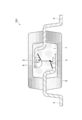
- FIG. 2 is a diagram illustrating a cross-sectional configuration of a photocoupler to which the present embodiment is applied.
- FIG. 2 is a diagram illustrating a cross-sectional configuration of a semiconductor layer forming substrate that is a source of a semiconductor light emitting element.
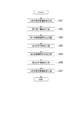
- 5 is a flowchart illustrating a method for manufacturing a semiconductor layer formation substrate.
- 5 is a flowchart illustrating a method for manufacturing an active layer.
- FIG. 2 is a diagram illustrating a cross-sectional configuration of a semiconductor light emitting device including a light emitting device layer.
- 5 is a flowchart illustrating a method for manufacturing a semiconductor light emitting device.
- FIG. 9 is a graph showing the relationship between the forward current and the 1st normalization luminous efficiency of each Example and each comparative example.
- FIG. 9 is a graph showing the relationship between the forward current and the second normalized luminous efficiency of the semiconductor light emitting devices according to the examples and the comparative examples.
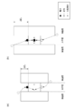
- (A) (b) is a figure which shows typically the band structure in the multiple quantum well structure of the semiconductor light emitting element which concerns on a comparative example and an Example.
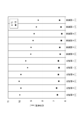
- FIG. 9 is a graph showing response times (rise time and fall time) of the semiconductor light emitting devices according to the examples and the comparative examples.
- FIG. 1 is a diagram showing a cross-sectional configuration of a photocoupler 100 to which the present embodiment is applied.
- a photocoupler 100 as an example of a light transmitting device includes a semiconductor light emitting element 2 that converts an electric signal into an optical signal and outputs the light signal, and a light received from the semiconductor light emitting element 2 while being arranged opposite to the semiconductor light emitting element 2. And a semiconductor light receiving element 3 for converting the light into an electric signal and outputting the electric signal.
- the photocoupler 100 includes a light emitting element side electrode 4 for supplying an electric signal (light emitting signal) to the semiconductor light emitting element 2 and a light receiving element side electrode 5 for acquiring an electric signal (light receiving signal) from the semiconductor light receiving element 3.
- the photocoupler 100 includes a lens 6 that has electrical insulation properties and a light-transmitting property with respect to light having the emission wavelength of the semiconductor light emitting element 2 and condenses light traveling from the semiconductor light emitting element 2 to the semiconductor light receiving element 3. ing. Furthermore, the photocoupler 100 has electrical insulating properties and a light-transmitting property with respect to light of the emission wavelength of the semiconductor light-emitting element 2, and a transparent resin housing the semiconductor light-emitting element 2, the semiconductor light-receiving element 3, and the lens 6 therein. A part 7 is provided.
- the photocoupler 100 has an electrically insulating property and a light-shielding property against the light having the emission wavelength of the semiconductor light emitting element 2, and includes an opaque resin part 8 that houses the transparent resin part 7 therein.
- the light emitting element side electrode 4 and the light receiving element side electrode 5 are each formed of a pair of conductors. One end of each is disposed inside the transparent resin part 7 and is used for electrical connection with the semiconductor light emitting element 2 or the semiconductor light receiving element 3. Is arranged to protrude outside the opaque resin portion 8 via the opaque resin portion 8 and is used for electrical connection with the outside.
- the semiconductor light emitting element 2 as an example of the light emitting element can be constituted by a stacked body of an inorganic semiconductor having a pn junction.
- the inorganic semiconductor a compound semiconductor is preferably used, and among them, a group III-V compound semiconductor is more preferably used.
- the semiconductor light emitting device 2 of the present embodiment has a well layer and a barrier between a p-type semiconductor layer having p-type conductivity and an n-type semiconductor layer having n-type conductivity, as described later.
- An active layer having a so-called multi quantum well (MQW) structure in which layers are alternately stacked is provided. The details of the semiconductor light emitting device 2 used in the present embodiment will be described later.
- MQW multi quantum well
- the semiconductor light-receiving element 3 as an example of the light-receiving element can be formed of an inorganic semiconductor laminate having a pn junction.
- the inorganic semiconductor a compound semiconductor is preferably used, and among them, a group III-V compound semiconductor is more preferably used.
- the semiconductor light receiving element 3 of the present embodiment needs to have sensitivity to the emission wavelength of the semiconductor light emitting element 2. Examples of the semiconductor light receiving element 3 include a photodiode, a phototransistor, and a phototriac.
- the light emitting element side electrode 4 can be made of a metal such as copper, a copper-based alloy, and an iron-based alloy, for example.
- the semiconductor light emitting element 2 is mounted and electrically connected to one of the pair of conductors constituting the light emitting element side electrode 4, and the other conductor is connected to the semiconductor light emitting element 2 via a bonding wire. Are electrically connected.
- the light-receiving element-side electrode 5 can also be made of a metal such as copper, a copper-based alloy, and an iron-based alloy.
- the semiconductor light receiving element 3 is mounted and electrically connected to one of the pair of conductors constituting the light receiving element side electrode 5, and the other is connected to the semiconductor light receiving element via a bonding wire. 3 are electrically connected.
- the lens 6 can be made of, for example, an uncolored silicone resin.
- the lens 6 has not only a light condensing function, but also a function of sealing the semiconductor light emitting element 2 by sandwiching the semiconductor light emitting element 2 between the lens 6 and the light emitting element side electrode 4.
- the transparent resin portion 7 can be made of, for example, an uncolored epoxy resin. Further, the transparent resin portion 7 also has a function of sealing the lens 6 that houses the semiconductor light emitting element 2 therein.
- the opaque resin portion 8 can be made of, for example, a colored (for example, black) epoxy resin.
- the opaque resin section 8 seals the transparent resin section 7 that houses the semiconductor light emitting element 2 and the lens 6 therein, and also has a function as a housing of the photocoupler 100.
- FIG. 2 is a diagram illustrating a cross-sectional configuration of a semiconductor layer forming substrate 1 that is a base of the semiconductor light emitting element 2.
- the semiconductor layer forming substrate 1 includes a growth substrate 1a, a base layer 1b stacked on the growth substrate 1a, and an etching stop layer 1c stacked on the base layer 1b.
- the semiconductor layer forming substrate 1 is formed by stacking a plurality of semiconductor layers on an etching stop layer 1c, and includes a light emitting element layer 10 that emits light when energized and a cap layer 1d stacked on the light emitting element layer 10.
- a light emitting element layer 10 that emits light when energized
- a cap layer 1d stacked on the light emitting element layer 10.
- the growth substrate 1a serves as a base for growing the base layer 1b, the etching stop layer 1c, the light emitting element layer 10, and the cap layer 1d.
- growth substrate 1a is made of a single crystal of a compound semiconductor. Examples of such a growth substrate 1a include GaAs and InP.
- the base layer 1b is a base for growing the etching stop layer 1c, the light emitting element layer 10, and the cap layer 1d on the growth substrate 1a.
- the underlayer 1b is composed of a compound semiconductor epitaxial film.
- the etching stop layer 1c extremely lowers the etching rate when the growth substrate 1a and the base layer 1b are separated from the light emitting element layer 10 by wet etching in a manufacturing process of the semiconductor light emitting element 2 described later, This is for suppressing the etching up to the layer 10.
- the etching stop layer 1c is composed of a compound semiconductor epitaxial film.
- the light emitting element layer 10 functions as a light emitting diode by providing an active layer having a multiple quantum well structure at a pn junction. In addition, the light emitting element layer 10 forms a main part of the semiconductor light emitting element 2 as described later.
- the light emitting element layer 10 includes a p-type contact layer 11 laminated on the etching stop layer 1c, a p-type current diffusion layer 12 laminated on the p-type contact layer 11, and a p-type current diffusion layer 12 laminated on the p-type current diffusion layer 12. And a mold clad layer 13.
- the light emitting element layer 10 includes an active layer 14 laminated on the p-type cladding layer 13, an n-type cladding layer 15 laminated on the active layer 14, and a cap layer 1d laminated on the n-type cladding layer 15. And an n-type current diffusion layer 16 to be stacked.
- components of the light emitting element layer 10 will be described in order.
- the p-type contact layer 11 using holes as carriers serves to provide a not-shown p-electrode (positive electrode section 20: see FIG. 5 described later).
- the p-type contact layer 11 of the present embodiment is made of a compound semiconductor that lattice-matches with the etching stop layer 1c.
- the p-type contact layer 11 is doped with a p-type impurity.
- the p-type current diffusion layer 12 having holes as carriers spreads the carriers (holes in this case) injected from the p-type contact layer 11 toward the active layer 14 in the plane direction, that is, applies a current in the plane direction. It is for spreading.
- the p-type current diffusion layer 12 of the present embodiment is made of a compound semiconductor that lattice-matches with the p-type contact layer 11. Further, it is preferable that the p-type current diffusion layer 12 is doped with a p-type impurity.
- the p-type current diffusion layer 12 is thicker than the p-type contact layer 11. Further, the p-type current diffusion layer 12 preferably has a larger band gap than the p-type contact layer 11. Further, p-type current diffusion layer 12 preferably contains a p-type impurity composed of the same element as p-type contact layer 11. Furthermore, the p-type current diffusion layer 12 preferably has a lower impurity concentration than the p-type contact layer 11.
- the p-type cladding layer 13 having holes as carriers injects carriers (here, holes) into the active layer 14 and, together with the n-type cladding layer 15, removes the injected carriers (here, holes and electrons). It is for confinement.
- the p-type cladding layer 13 as an example of the p-type semiconductor layer is made of a compound semiconductor that lattice-matches with the p-type current diffusion layer 12. Further, it is preferable that the p-type cladding layer 13 is doped with a p-type impurity.
- the thickness of the p-type cladding layer 13 is smaller than that of the p-type current diffusion layer 12. Further, it is preferable that the p-type cladding layer 13 has a larger band gap than the p-type current diffusion layer 12. Further, the p-type cladding layer 13 preferably contains a p-type impurity made of the same element as the p-type current diffusion layer 12. Furthermore, the p-type cladding layer 13 preferably has a lower impurity concentration than the p-type current diffusion layer 12.
- the active layer 14 as an example of the light emitting layer is a layer that emits light by recombination of electrons and holes due to energization. Further, the active layer 14 of the present embodiment has a so-called multiple quantum well structure (MQW). Note that the active layer 14 basically does not include a p-type impurity and an n-type impurity. However, during manufacturing, p-type impurities may diffuse from the p-type cladding layer 13 or n-type impurities may diffuse from the n-type cladding layer 15.
- MQW multiple quantum well structure
- the active layer 14 of the present embodiment includes a p-side external barrier layer 141 laminated on the p-type cladding layer 13, a first well layer 1421 laminated on the p-side external barrier layer 141, and a first well layer 1421.
- the n-type cladding layer 1423 includes a third well layer 1423 stacked on the 1432, and an n-side external barrier layer 144 stacked on the third well layer 1423 and on which the n-type cladding layer 15 is stacked.
- the active layer 14 of the present embodiment includes three well layers (first well layer 1421 to third well layer 1423) and a barrier layer (p-side external barrier) having one more layer than the well layer.
- the first well layer 1421 to the third well layer 1423 may be collectively referred to as a well layer 142.
- the first internal barrier layer 1431 and the second internal barrier layer 1432 may be collectively referred to as an internal barrier layer 143.
- the p-side external barrier layer 141, the internal barrier layer 143, and the n-side external barrier layer 144 may be collectively referred to as a barrier layer.
- the p-side external barrier layer 141 as an example of the p-side barrier layer is a layer that sandwiches the first well layer 1421 together with the first internal barrier layer 1431.
- the p-side external barrier layer 141 of the present embodiment is made of a compound semiconductor that lattice-matches with the p-type cladding layer 13 and the well layer 142.
- the first well layer 1421 forming the well layer 142 is a layer sandwiched between the p-side external barrier layer 141 and the first internal barrier layer 1431 adjacent to the first well layer 1421.
- the second well layer 1422 constituting the well layer 142 is a layer sandwiched between the first internal barrier layer 1431 and the second internal barrier layer 1432 adjacent to itself.
- the third well layer 1423 constituting the well layer 142 is a layer sandwiched between the second internal barrier layer 1432 and the n-side external barrier layer 144 adjacent thereto.
- the well layer 142 of the present embodiment is made of a compound semiconductor that lattice-matches with the barrier layer.
- the first internal barrier layer 1431 constituting the internal barrier layer 143 is a layer sandwiching the first well layer 1421 together with the p-side external barrier layer 141 on one side, and the second internal barrier layer 1432 on the other side. In addition, it is a layer sandwiching the second well layer 1422.
- the second internal barrier layer 1432 constituting the internal barrier layer 143 is a layer sandwiching the second well layer 1422 together with the first internal barrier layer 1431 on one side, and has an n-side external barrier layer on the other side. This is a layer for sandwiching the third well layer 1423 together with the layer 144.
- the internal barrier layer 143 of the present embodiment is made of a compound semiconductor that lattice-matches with the well layer 142.
- the n-side external barrier layer 144 as an example of the n-side barrier layer is a layer for sandwiching the third well layer 1423 together with the second internal barrier layer 1432.
- the n-side external barrier layer 144 of the present embodiment is made of a compound semiconductor that lattice-matches with the well layer 142 and the n-type cladding layer 15.
- the well layer 142 (first well layer 1421 to third well layer 1423) of this embodiment is (Al x Ga 1 -x ) y In 1 -y As z P 1 -z (0 ⁇ x ⁇ 0.2 , 0.7 ⁇ y ⁇ 1.0, 0.7 ⁇ z ⁇ 1.0).
- the well layer 142 is preferably formed of In a Ga 1-a As (0 ⁇ a ⁇ 0.4) among the above compositions.
- the emission wavelength is 850 ⁇ 20 nm
- the appropriate In composition of the well layer 142 varies depending on the thickness of the well layer 142, the number of the well layers 142, and the composition of the barrier layer described later.
- the well layer 142 is preferably made of a direct transition type compound semiconductor.
- In corresponds to the first group III element
- Ga corresponds to the second group III element
- Al corresponds to the third group III element.
- the barrier layers (the p-side external barrier layer 141, the internal barrier layer 143, and the n-side external barrier layer 144) are made of Al u Ga 1-u As (0 ⁇ u ⁇ 1) or (Al v Ga 1 ⁇ ).
- b It is composed of w In 1 ⁇ w P (0 ⁇ v ⁇ 1, 0.4 ⁇ w ⁇ 0.6).
- the barrier layer is preferably composed of Al b Ga 1-b As (0.3 ⁇ b ⁇ 0.45) among the above compositions. Further, it is desirable that the barrier layer is also made of a direct transition type compound semiconductor.
- the active layer 14 having a multiple quantum well structure compound semiconductors constituting each are selected such that the band gap of the barrier layer is larger than the band gap of the well layer 142.
- the material is selected such that the difference in band gap between the barrier layer and the well layer 142 is 0.6 eV or more.
- the well layer 142 is made of (Al x Ga 1 -x ) y In 1 -y As z P 1 -z (0 ⁇ x ⁇ 0.2, 0.7 ⁇ y ⁇ 1.0, 0.7 ⁇ z ⁇ 1.0), the emission wavelength is in the range of 730 nm to 1050 nm.
- the well layer 142 is made of In a Ga 1 ⁇ a As (0 ⁇ a ⁇ 0.4)
- the emission wavelength is in the range of 800 nm to 1050 nm.
- the first well layer 1421 preferably has a smaller thickness than the p-side external barrier layer 141. Further, it is preferable that the first internal barrier layer 1431 be thicker than the first well layer 1421. Further, the second well layer 1422 preferably has a smaller thickness than the first internal barrier layer 1431. Furthermore, it is preferable that the thickness of the second internal barrier layer 1432 is larger than that of the second well layer 1422. In addition, the third well layer 1423 preferably has a smaller thickness than the second internal barrier layer 1432. The thickness of the n-side external barrier layer 144 is preferably larger than that of the third well layer 1423.
- each layer (the p-side external barrier layer 141, the first internal barrier layer 1431, the second internal barrier layer 1432, and the n-side external barrier layer 144) constituting the barrier layer is composed of each layer (the first well) constituting the well layer 142. It is preferable that the thickness be larger than those of the layers 1421 to the third well layer 1423).
- the thickness of the p-side external barrier layer 141 is larger than that of the p-type cladding layer 13. It is preferable that the p-type cladding layer 13 has a band gap larger than or the same as that of the p-side external barrier layer 141.
- the n-type cladding layer 15 has a larger thickness than the n-side external barrier layer 144. It is preferable that the n-type cladding layer 15 has a band gap larger than or the same as that of the n-side external barrier layer 144.
- the p-side external barrier layer 141 is thicker than the layers (the first internal barrier layer 1431 and the second internal barrier layer 1432) constituting the internal barrier layer 143. It is preferable that the p-side external barrier layer 141 has a band gap larger or equal to each of the layers constituting the internal barrier layer 143.
- the n-side external barrier layer 144 is thicker than each layer (the first internal barrier layer 1431 and the second internal barrier layer 1432) constituting the internal barrier layer 143. It is preferable that the n-side external barrier layer 144 has a band gap larger than or the same as each of the layers constituting the internal barrier layer 143.
- the p-side external barrier layer 141 is thicker than the n-side external barrier layer 144.
- the p-side external barrier layer 141 and the n-side external barrier layer 144 preferably have the same band gap.
- first internal barrier layer 1431 and the second internal barrier layer 1432 forming the internal barrier layer 143 have the same thickness. It is preferable that the first internal barrier layer 1431 and the second internal barrier layer 1432 have the same band gap.
- first well layer 1421, the second well layer 1422, and the third well layer 1423 forming the well layer 142 have the same thickness.
- the first well layer 1421, the second well layer 1422, and the third well layer 1423 preferably have the same band gap.
- the n-type cladding layer 15 using electrons as carriers serves to inject carriers (here, electrons) into the active layer 14 and to confine the injected carriers (here, holes and electrons) together with the p-type cladding layer 13. belongs to.
- the n-type cladding layer 15 as an example of the n-type semiconductor layer is formed of a compound semiconductor that lattice-matches with the n-side external barrier layer 144.
- the n-type cladding layer 15 is doped with an n-type impurity.
- the n-type current diffusion layer 16 using electrons as carriers serves to provide an n-electrode (negative electrode part 30: see FIG. 5 described later) not shown.
- the n-type current diffusion layer 16 is for spreading carriers (here, electrons) injected from the outside in the plane direction toward the active layer 14, that is, for diffusing current in the plane direction.
- the n-type current diffusion layer 16 of the present embodiment also has a function as an n-type contact layer.
- the n-type current spreading layer 16 of the present embodiment is made of a compound semiconductor that lattice-matches with the n-type cladding layer 15. Further, it is preferable that the n-type current diffusion layer 16 is doped with an n-type impurity.
- the n-type current diffusion layer 16 is thicker than the n-type cladding layer 15. Further, it is preferable that the n-type current diffusion layer 16 has a smaller band gap than the n-type cladding layer 15. Further, the n-type current diffusion layer 16 preferably contains an n-type impurity composed of the same element as the n-type cladding layer 15. Furthermore, the n-type current diffusion layer 16 preferably has a lower impurity concentration than the n-type cladding layer 15.
- n-type current diffusion layer 16 also serves as the n-type contact layer, no separate n-type contact layer is provided.
- the present invention is not limited to this, and an n-type contact layer may be provided on the n-type current diffusion layer 16.
- the thickness of the p-type current diffusion layer 12 is larger than that of the n-type current diffusion layer 16. Further, it is preferable that the p-type current diffusion layer 12 and the n-type current diffusion layer 16 have the same band gap. Preferably, the p-type current diffusion layer 12 has a higher impurity concentration than the n-type current diffusion layer 16.
- the p-type cladding layer 13 and the n-type cladding layer 15 have the same thickness. Further, it is preferable that the p-type cladding layer 13 and the n-type cladding layer 15 have the same band gap.
- the p-type cladding layer 13 preferably has a lower impurity concentration than the n-type cladding layer 15.
- the cap layer 1d is for suppressing release of various Group V elements (for example, As and P) from the light emitting element layer 10 laminated on the growth substrate 1a and the like.
- the cap layer 1d of the present embodiment is made of a compound semiconductor that lattice-matches with the n-type current diffusion layer 16.
- FIG. 3 is a flowchart for explaining a method of manufacturing the semiconductor layer forming substrate 1 shown in FIG.
- the semiconductor layer forming substrate 1 of the present embodiment is obtained by forming each layer on the growth substrate 1a by using MOCVD (Metal Organic Chemical Vapor Deposition).
- MOCVD Metal Organic Chemical Vapor Deposition
- the present invention is not limited to this, and for example, an MBE (Molecular Beam Epitaxy) method may be used.
- Step 10 a carrier gas and a source gas of each element constituting the underlayer 1b are supplied into a chamber in which the growth substrate 1a is installed (Step 10). In step 10, the underlayer 1b is laminated on the growth substrate 1a.
- step 20 a carrier gas is continuously supplied into the chamber in which the growth substrate 1a on which the base layer 1b is stacked is provided, and a source gas of each element constituting the etching stop layer 1c is supplied (step 20).
- step 20 the etching stop layer 1c is laminated on the underlayer 1b.
- Step 30 a carrier gas and a source gas of each element constituting the p-type contact layer 11 are supplied into the chamber in which the growth substrate 1a on which the etching stop layer 1c is stacked is installed (Step 30). .
- step 30 the p-type contact layer 11 is laminated on the etching stop layer 1c.
- step 40 a carrier gas is continuously supplied into the chamber in which the growth substrate 1a on which the layers up to the p-type contact layer 11 are stacked is provided, and a source gas of each element constituting the p-type current diffusion layer 12 is supplied (step 40). ). In step 40, the p-type current diffusion layer 12 is laminated on the p-type contact layer 11.
- [P-type cladding layer forming step] Then, a carrier gas is continuously supplied into the chamber in which the growth substrate 1a on which the layers up to the p-type current diffusion layer 12 are stacked is provided, and a source gas of each element constituting the p-type cladding layer 13 is supplied (step 50). ). In step 50, the p-type cladding layer 13 is laminated on the p-type current diffusion layer 12.
- the carrier gas is continuously supplied into the chamber in which the growth substrate 1a on which the p-type cladding layer 13 is laminated is provided, and the source gas of each element constituting the active layer 14 is supplied (step 60).
- the active layer 14 is laminated on the p-type cladding layer 13. A more detailed manufacturing method of the active layer 14 will be described later.
- step 70 a carrier gas is continuously supplied into the chamber in which the growth substrate 1a on which the active layer 14 is laminated is provided, and a source gas of each element constituting the n-type clad layer 15 is supplied (step 70).
- step 70 the n-type cladding layer 15 is laminated on the active layer 14.
- Step of forming n-type current diffusion layer Subsequently, a carrier gas is continuously supplied into the chamber in which the growth substrate 1a on which the n-type cladding layer 15 is stacked is provided, and a source gas of each element constituting the n-type current diffusion layer 16 is supplied (step). 80). In step 80, the n-type current spreading layer 16 is laminated on the n-type cladding layer 15.
- cap layer forming step Then, the carrier gas is continuously supplied into the chamber in which the growth substrate 1a on which the n-type current diffusion layer 16 is stacked is provided, and the source gas of each element constituting the cap layer 1d is supplied (step 90). In step 90, the cap layer 1d is laminated on the n-type current diffusion layer 16. As described above, the semiconductor layer forming substrate 1 in which the base layer 1b, the etching stop layer 1c, the light emitting element layer 10, and the cap layer 1d are laminated in this order on the growth substrate 1a is obtained.
- FIG. 4 is a flowchart for explaining a method for manufacturing the active layer 14.
- step 61 a carrier gas is continuously supplied into the chamber in which the growth substrate 1a on which the p-type cladding layer 13 is stacked is provided, and a source gas of each element constituting the p-side external barrier layer 141 is supplied (step 61). ). In step 61, the p-side external barrier layer 141 is laminated on the p-type cladding layer 13.
- step 62 a carrier gas is continuously supplied into the chamber in which the growth substrate 1a in which the p-side external barrier layer 141 is stacked is provided, and a source gas of each element constituting the first well layer 1421 is supplied (step). 62). In step 62, the first well layer 1421 is stacked on the p-side external barrier layer 141.
- step 63 First internal barrier layer forming step
- a carrier gas is continuously supplied into the chamber in which the growth substrate 1a having the first well layer 1421 is stacked, and a source gas of each element constituting the first internal barrier layer 1431 is supplied (step). 63).
- the first inner barrier layer 1431 is stacked on the first well layer 1421.
- step 64 a carrier gas is continuously supplied into the chamber in which the growth substrate 1a on which the first internal barrier layer 1431 is stacked is provided, and a source gas of each element constituting the second well layer 1422 is supplied (step 64). ). In step 64, the second well layer 1422 is stacked on the first internal barrier layer 1431.
- step 65 a carrier gas is continuously supplied into the chamber in which the growth substrate 1a in which the second well layer 1422 is stacked is provided, and a source gas of each element constituting the second internal barrier layer 1432 is supplied (step). 65). In step 65, a second internal barrier layer 1432 is stacked on the second well layer 1422.
- step 66 a carrier gas is continuously supplied into the chamber in which the growth substrate 1a on which the second inner barrier layer 1432 is stacked is provided, and a source gas of each element constituting the third well layer 1423 is supplied (step). 66). In step 66, the third well layer 1423 is stacked on the second inner barrier layer 1432.
- Step of forming n-side external barrier layer Then, the carrier gas is continuously supplied into the chamber in which the growth substrate 1a in which the third well layer 1423 is stacked is provided, and the source gas of each element constituting the n-side external barrier layer 144 is supplied (step 67). ). In step 67, the n-side external barrier layer 144 is stacked on the third well layer 1423. As described above, the p-side external barrier layer 141, the internal barrier layer 143 (the first internal barrier layer 1431 and the second internal barrier layer 1432), the n-side external barrier layer 144, and the well layer 142 (the first well layer 1421 to the third The active layer 14 including the well layer 1423) is obtained.
- FIG. 5 is a diagram illustrating a cross-sectional configuration of the semiconductor light emitting element 2 including the light emitting element layer 10.
- the semiconductor light emitting element 2 is obtained by performing various processes using the above-described semiconductor layer forming substrate 1 as a starting material. However, as is evident from FIG. 5, the semiconductor light emitting element 2 includes the light emitting element layer 10, while forming the semiconductor layer forming substrate 1 together with the light emitting element layer 10, the growth substrate 1a, the base layer 1b, and the etching stop. It does not include the layer 1c and the cap layer 1d.
- the semiconductor light-emitting element 2 is connected to the above-described light-emitting element layer 10, the positive electrode portion 20 connected to the p-type contact layer 11 of the light-emitting element layer 10, and the n-type current diffusion layer 16 of the light-emitting element layer 10. And a negative electrode section 30.
- the positive electrode section 20 functions as a p-electrode of the light emitting element layer 10.
- the negative electrode section 30 functions as an n-electrode of the light-emitting element layer 10.
- the negative electrode section 30 also functions as a reflection film that reflects light output from the light emitting element layer 10 to the negative electrode section 30 side to the positive electrode section 20 side.
- the negative electrode portion 30 is formed substantially on the entire lower surface of the semiconductor light emitting element 2 in the drawing.
- the positive electrode section 20 is formed in an island shape in a partial region on the upper side of the semiconductor light emitting element 2 in the drawing.
- the negative electrode section 30 includes an n-electrode layer 31 laminated on the n-type current diffusion layer 16 of the light-emitting element layer 10, a reflection layer 32 laminated on the n-electrode layer 31, and a diffusion prevention layer laminated on the reflection layer 32. 33.
- the negative electrode portion 30 includes a bonding layer 34 stacked on the diffusion preventing layer 33, an internal electrode layer 35 stacked on the bonding layer 34, a support substrate 36 stacked on the internal electrode layer 35, and a support substrate 36. And an external electrode layer 37 which is stacked on the substrate and exposed to the outside.
- the n-electrode layer 31 is provided to diffuse and supply a current to the light emitting element layer 10 in the plane direction.
- the n-electrode layer 31 includes a light-transmitting layer 311 provided with a plurality of through holes penetrating in the thickness direction, and a plurality of columnar electrode layers 312 provided to fill each of the plurality of through holes. have.
- the light transmitting layer 311 has an insulating property and transmits light output from the light emitting element layer 10. Then, SiO 2 or the like can be used for the light-transmitting layer 311.
- the columnar electrode layer 312 has conductivity and makes ohmic contact with the n-type current diffusion layer 16 of the light emitting element layer 10. Then, AuGe or the like can be used for the columnar electrode layer 312.
- the reflection layer 32 has conductivity and reflects light output from the light emitting element layer 10.
- a metal such as AgPdCu (APC) alloy, Au, Cu, Ag, Al, Pt, or an alloy thereof can be used.
- the diffusion prevention layer 33 has conductivity, and is provided to suppress the metal included in the bonding layer 34 and the support substrate 36 from diffusing toward the reflection layer 32 and reacting with the reflection layer 32.
- the diffusion prevention layer 33 can be made of a metal such as Ni, Ti, Pt, Cr, Ta, W, and Mo. Alternatively, a plurality of metal layers selected from these may be laminated. it can.
- the bonding layer 34 has conductivity and is provided for bonding the diffusion preventing layer 33 formed on the light emitting element layer 10 and the internal electrode layer 35 formed on the support substrate 36.
- an Au-based eutectic metal that is chemically stable and has a low melting point can be used.
- examples of the Au-based eutectic metal include AuGe, AuSn, AuSi, and AuIn.
- the internal electrode layer 35 has conductivity and is provided for electrically connecting the bonding layer 34 and the support substrate 36.
- Various metal materials can be used for the internal electrode layer 35, and a configuration in which a plurality of metal layers are stacked can be used.
- the support substrate 36 has conductivity and is provided to physically support the light emitting element layer 10 obtained by removing the growth substrate 1a and the like from the semiconductor layer forming substrate 1.
- a material that absorbs light output from the light emitting element layer 10 can be used as the support substrate 36.
- a semiconductor wafer for example, a Ge wafer, a Si wafer, a GaAs wafer, a GaP wafer, or the like can be used.
- the external electrode layer 37 has conductivity and is provided to be electrically connected to a wiring (not shown) provided outside.
- Various metal materials can be used for the external electrode layer 37, and a plurality of metal layers can be stacked.
- FIG. 6 is a flowchart for explaining a method for manufacturing the semiconductor light emitting device 2.
- cap layer removal step First, the cap layer 1d is removed from the semiconductor layer forming substrate 1 (step 100). Thereby, the n-type current diffusion layer 16 constituting the light emitting element layer 10 is exposed on the surface of the semiconductor layer forming substrate 1, that is, on the surface opposite to the growth substrate 1a.
- Step 110 the negative electrode section 30 is formed on the n-type current diffusion layer 16 of the semiconductor layer forming substrate 1 having the growth substrate 1a, the base layer 1b, the etching stop layer 1c, and the light emitting element layer 10 (Step 110).
- the negative electrode portion forming step of Step 110 includes a plurality of steps (Step 111 to Step 117 in this example) described below.
- Step of forming n-electrode layer In the negative electrode portion forming step of Step 110, first, the n-electrode layer 31 is formed on the n-type current diffusion layer 16 of the light emitting element layer 10 (Step 111). However, in the n-electrode layer forming step of Step 111, the light-transmitting layer 311 is formed first (Step 111a), and then the columnar electrode layer 312 is formed (Step 111b).
- Transparent layer forming step In the light-transmitting layer forming step of Step 111a, after a layer of SiO 2 is deposited over the entire surface of the n-type current diffusion layer 16 by CVD, a hole to be formed on the columnar electrode layer 312 is formed by etching to form a plurality of holes. A through hole is formed. At this time, the thickness of SiO 2 is about 0.3 ⁇ m. Thereby, the light transmitting layer 311 made of SiO 2 is obtained.
- Step 111b In the columnar electrode layer forming step of Step 111b, AuGe is filled in each of the plurality of through holes formed in the light transmitting layer 311 by vapor deposition to form a plurality of columnar electrode layers 312. At this time, the thickness of AuGe is the same as the thickness of the light transmitting layer 311. As described above, the n-electrode layer 31 including the light-transmitting layer 311 and the plurality of columnar electrode layers 312 is obtained.
- the thickness of the reflection layer 32 is about 0.7 ⁇ m.
- Step 113 the thickness of the diffusion preventing layer 33 is about 0.5 ⁇ m.
- the bonding layer 34 is formed by vapor deposition to form the bonding layer 34 (Step 114).
- the thickness of the bonding layer 34 is about 1.0 ⁇ m.
- the n-electrode layer 31, the reflection layer 32, the diffusion prevention layer 33, and the bonding layer 34 are laminated on the n-type current diffusion layer 16 in the light emitting element layer 10 of the semiconductor layer forming substrate 1 excluding the cap layer 1d. It is in a state of being left.
- a structure in which the n-electrode layer 31 to the bonding layer 34 are stacked on the semiconductor layer forming substrate 1 excluding the cap layer 1d is referred to as a “first stacked body”.
- a support substrate 36 made of a Ge wafer is prepared separately from the first stacked body. Then, on one surface (front surface) of the support substrate 36, Pt and Au are laminated in this order by vapor deposition, and an internal electrode layer 35 formed by laminating a Pt layer and an Au layer is formed (Step 115). At this time, the thickness of the internal electrode layer 35 is about 0.1 ⁇ m for the Pt layer and about 0.5 ⁇ m for the Au layer.
- Step 116 Next, on the other surface (back surface) of the support substrate 36, Pt and Au are laminated in this order by vapor deposition, and an external electrode layer 37 formed by laminating a Pt layer and an Au layer is formed (Step 116). At this time, the thickness of the external electrode layer 37 is about 0.1 ⁇ m for the Pt layer and about 0.5 ⁇ m for the Au layer. At this time, the internal electrode layer 35 is laminated on the front surface of the support substrate 36, and the external electrode layer 37 is laminated on the rear surface thereof.
- a structure in which the internal electrode layer 35 and the external electrode layer 37 are laminated on the support substrate 36 is referred to as a “second laminate”.
- Step 117 The heating temperature is about 400 ° C., and the applied pressure is about 500 kgf.
- the semiconductor layer forming substrate 1 including the growth substrate 1a and the light emitting element layer 10 and the negative electrode portion 30 including the support substrate 36 are in a laminated state.
- a product obtained by laminating both of them is referred to as a “third laminate”.
- the negative electrode portion forming step of Step 110 is completed.
- the light emitting element layer 10 is separated from the growth substrate 1a, the base layer 1b and the etching stop layer 1c in the semiconductor layer forming substrate 1 by performing wet etching on the third stacked body.
- the growth substrate 1a is removed from (step 120).
- the light emitting element layer 10 and the negative electrode section 30 are in a laminated state, and the p-type contact layer 11 of the light emitting element layer 10 is exposed to the outside.
- a laminate of the light emitting element layer 10 and the negative electrode unit 30 is referred to as a “fourth laminate”. It is desirable that the base layer 1b and the etching stop layer 1c are completely removed by polishing the p-type contact layer 11 side of the fourth laminate as necessary.
- a plurality of positive electrode portions 20 are formed on the p-type contact layer 11 of the light emitting element layer 10 in the fourth stacked body (Step 130).
- an AuBe-Ni alloy, Ti and Au are laminated in this order on the p-type contact layer 11 by vapor deposition, and a positive electrode section 20 formed by laminating an AuBe-Ni alloy layer, a Ti layer and an Au layer in this order.
- the thickness of the positive electrode portion 20 is about 0.5 ⁇ m for the AuBe—Ni alloy layer, about 0.2 ⁇ m for the Ti layer, and about 1.0 ⁇ m for the Au layer.
- the plurality of positive electrode portions 20 are formed on the surface of the light-emitting element layer 10 where the p-type contact layer 11 is formed in the fourth stacked body in which the light-emitting element layer 10 and the negative electrode portion 30 are stacked. Are arranged on the matrix.
- a structure in which the negative electrode portion 30 and the plurality of positive electrode portions 20 are stacked on the light emitting element layer 10 is referred to as a “fifth stacked body”.
- Step 140 a region of the p-type contact layer 11 in the fifth stacked body that is exposed to the outside without being covered by the plurality of positive electrode portions 20 is removed by wet etching or the like.
- a part of the p-type current diffusion layer 12 existing on the p-type contact layer 11 side is also removed. .
- minute irregularities due to wet etching have been formed.
- a part obtained by removing each of the p-type contact layer 11 and the p-type current diffusion layer 12 from the fifth stacked body is referred to as a “sixth stacked body”.
- the sixth stacked body is divided into a plurality of semiconductor light emitting elements 2 (step 150).
- the semiconductor light emitting elements 2 are singulated so that each of the semiconductor light emitting elements 2 includes one positive electrode section 20.
- the semiconductor light emitting device 2 shown in FIG. 5 having the light emitting device layer 10, the positive electrode portion 20, and the negative electrode portion 30 is obtained.
- the thus obtained semiconductor light emitting element 2, semiconductor light receiving element 3, light emitting element side electrode 4, light receiving element side electrode 5, lens 6, transparent resin part 7, and opaque resin part 8 Is used to obtain the photocoupler 100 shown in FIG.
- the semiconductor light receiving element 3 When the light from the semiconductor light emitting element 2 is received by the semiconductor light receiving element 3, the semiconductor light receiving element 3 outputs a light receiving signal corresponding to the amount of received light. This light receiving signal is output to the outside via the light receiving element side electrode 5. During this time, the opaque resin portion 8 restricts the light from the outside from reaching the semiconductor light receiving element 3, and suppresses the noise from being mixed into the light receiving signal.
- signals can be transmitted while being optically coupled but electrically insulated.
- a light emission signal such as a pulse signal modulated by a predetermined method
- high-speed data communication can be performed via the photocoupler 100.
- the well layer 142 forming the active layer 14 is formed of three layers of the first well layer 1421 to the third well layer 1423.
- the number of the well layers 142 is appropriately changed by design. You can do it.
- the number of the well layers 142 is 10 or less, and more preferably 5 layers. It is desirable to make the following.
- the thickness of each layer constituting the well layer 142 is preferably a thickness at which a quantum effect can be obtained, and is preferably in the range of 3.3 nm to 7 nm.
- a p-type semiconductor layer (p-type contact layer 11, p-type current diffusion layer 12, and p-type cladding layer 13), an active layer 14, and an n-type semiconductor layer (n-type) are formed on growth substrate 1a.
- the semiconductor layer forming substrate 1 was obtained, but the present invention is not limited to this.
- the semiconductor layer forming substrate 1 may be obtained by forming an n-type semiconductor layer, an active layer 14 and a p-type semiconductor layer in this order on the growth substrate 1a.
- the configuration in which the semiconductor light emitting element 2 including the light emitting element layer 10 includes the reflective layer 32 has been described as an example. However, the structure of the semiconductor light emitting element 2 is appropriately designed and changed. No problem.
- the photocoupler 100 is configured using the semiconductor light emitting element 2 has been described as an example, but the present invention is not limited to this.
- the semiconductor light emitting element 2 may be used alone as a light source or the like, or a photo interrupter (an example of a light transmission device) for detecting the presence or absence and position of an object may be configured together with the semiconductor light receiving element 3.
- the present inventor manufactured the semiconductor layer forming substrate 1 in which the configuration of the active layer 14 was variously changed, and evaluated various characteristics of the semiconductor light emitting element 2 obtained from the semiconductor layer forming substrate 1.
- Table 1 shows the layer configuration of the semiconductor layer forming substrate 1 of Example 1
- Table 2 shows the layer configuration of Example 2
- Table 3 shows the layer configuration of the semiconductor layer forming substrate 1 of Example 3.
- Table 4 shows the layer configuration of each of the semiconductor light emitting elements 2 of Comparative Example 1
- Table 5 shows the layer configuration of Comparative Example 2
- Table 6 shows the layer configuration of each semiconductor light emitting element 2 of Comparative Example 3.
- the growth substrate 1a As the growth substrate 1a, a wafer made of GaAs single crystal to which Zn (zinc) as a p-type impurity was added was used. The thickness of the growth substrate 1a was set to 350 ( ⁇ m), and the off-angle of the crystal growth surface of the growth substrate 1a was set to 15 ° (referred to as “15offA” in Table 1, the same applies hereinafter).
- Al 0.25 Ga 0.25 In 0.5 P (described in Table 1 as “Al 0.25 Ga 0.25 In 0.5 P”, and the same hereinafter) was used.
- Mg (magnesium) as a p-type impurity was added to the etching stop layer 1c so as to have a concentration of 1.0 ⁇ 10 18 .
- the thickness of the etching stop layer 1c was 0.5 ( ⁇ m).
- the configuration of the light emitting element layer 10 is as follows.
- the light emission wavelength (design value) of the light emitting element layer 10 (more specifically, the active layer 14) was 850 nm.
- (P-type contact layer) GaAs was used for the p-type contact layer 11.
- C which is a p-type impurity, was added to the p-type contact layer 11 so as to have a concentration of 8.0 ⁇ 10 19 .
- the thickness of the p-type contact layer 11 was 0.05 ( ⁇ m).
- P-type current diffusion layer For the p-type current diffusion layer 12, Al 0.25 Ga 0.75 As was used. C, which is a p-type impurity, was added to the p-type current diffusion layer 12 so as to have a concentration of 1.0 ⁇ 10 18 . The thickness of the p-type current diffusion layer 12 was 5 ( ⁇ m).
- (P-type cladding layer) Al 0.45 Ga 0.55 As was used for the p-type cladding layer 13.
- C which is a p-type impurity, was added to the p-type cladding layer 13 so as to have a concentration of 8.0 ⁇ 10 17 .
- the thickness of the p-type cladding layer 13 was 0.2 ( ⁇ m).
- the structure of the active layer 14 is as follows.
- the p-side external barrier layer 141 Al 0.45 Ga 0.55 As was used.
- the p-side external barrier layer 141 is not doped with a p-type impurity and an n-type impurity (undoped (referred to as “UN” in Table 1, hereinafter the same)).
- the thickness of the p-side external barrier layer 141 was 0.3 ( ⁇ m).
- First well layer For the first well layer 1421, In 0.19 Ga 0.81 As was used. The p-type impurity and the n-type impurity are not added to the first well layer 1421. The thickness of the first well layer 1421 was 0.004 ( ⁇ m).
- first internal barrier layer 1431 Al 0.45 Ga 0.55 As was used.
- the first internal barrier layer 1431 is not doped with a p-type impurity and an n-type impurity.
- the thickness of the first internal barrier layer 1431 was set to 0.007 ( ⁇ m).
- the second well layer 1422 In 0.19 Ga 0.81 As was used. The p-type impurity and the n-type impurity are not added to the second well layer 1422. The thickness of the second well layer 1422 was 0.004 ( ⁇ m).
- the second internal barrier layer 1432 Al 0.45 Ga 0.55 As was used. The p-type impurity and the n-type impurity are not added to the second internal barrier layer 1432. The thickness of the second internal barrier layer 1432 was 0.007 ( ⁇ m).
- the third well layer 1423 In 0.19 Ga 0.81 As was used.
- the third well layer 1423 is not doped with a p-type impurity and an n-type impurity.
- the thickness of the third well layer 1423 was 0.004 ( ⁇ m).
- [N-side external barrier layer] Al 0.45 Ga 0.55 As was used for the n-side external barrier layer 144.
- the p-type impurity and the n-type impurity are not added to the n-side external barrier layer 144.
- the thickness of the n-side external barrier layer 144 was 0.05 ( ⁇ m).
- N-type cladding layer For the n-type cladding layer 15, Al 0.45 Ga 0.55 As was used. Te (tellurium), which is an n-type impurity, was added to the n-type cladding layer 15 so as to have a concentration of 1.0 ⁇ 10 18 . The thickness of the n-type cladding layer 15 was 0.2 ( ⁇ m).
- N-type current diffusion layer For the n-type current diffusion layer 16, Al 0.25 Ga 0.75 As was used. Te, which is an n-type impurity, was added to the n-type current diffusion layer 16 so as to have a concentration of 5.0 ⁇ 10 17 . The thickness of the n-type current diffusion layer 16 was 3.5 ( ⁇ m).
- Cap layer GaAs was used for the cap layer 1d. No p-type impurity or n-type impurity is added to the cap layer 1d. The thickness of the cap layer 1d was 0.1 ( ⁇ m).
- the semiconductor layer forming substrate 1 of Example 2 has the same configuration as that of the semiconductor layer forming substrate 1 according to the first embodiment except for the constituent materials of the respective layers forming the active layer 14.
- the barrier layers (the p-side external barrier layer 141, the first internal barrier layer 1431, the second internal barrier layer 1432, and the n-side external barrier layer 144) constituting the active layer 14 are formed.
- the well layer 142 (first well layer 1421 to third well layer 1423) constituting the active layer 14 has a lower ratio of In (Ga) than in the first embodiment. Ratio is high), and In 0.18 Ga 0.82 As was used.
- the semiconductor layer forming substrate 1 according to the third embodiment has the same configuration as the semiconductor layer forming substrate 1 according to the first and second embodiments except for the constituent materials of the respective layers forming the active layer 14.
- the barrier layers (the p-side external barrier layer 141, the first internal barrier layer 1431, the second internal barrier layer 1432, and the n-side external barrier layer 144) constituting the active layer 14 are formed.
- Al 0.30 Ga 0.70 As which has a lower Al ratio (a higher Ga ratio) than Example 2, was used.
- the well layer 142 (first well layer 1421 to third well layer 1423) constituting the active layer 14 has a lower ratio of In (Ga) than in the second embodiment. Ratio is high), and In 0.16 Ga 0.84 As was used.
- the semiconductor layer forming substrate 1 of Comparative Example 1 has the same configuration as the semiconductor layer forming substrates 1 of Examples 1 to 3, except for the constituent materials of each layer forming the active layer 14.
- the barrier layers (the p-side external barrier layer 141, the first internal barrier layer 1431, the second internal barrier layer 1432, and the n-side external barrier layer 144) constituting the active layer 14 are formed. ), Al 0.25 Ga 0.75 As having a lower ratio of Al (higher ratio of Ga) than that of Example 3 was used.
- the well layer 142 (first well layer 1421 to third well layer 1423) constituting the active layer 14 has a lower ratio of In (Ga) than in Example 3. Ratio is high), and In 0.14 Ga 0.86 As was used.
- the semiconductor layer forming substrate 1 of Comparative Example 2 has the same configuration as the semiconductor layer forming substrate 1 of Examples 1 to 3 and Comparative Example 1, except for the constituent materials of each layer forming the active layer 14.
- the barrier layers (the p-side external barrier layer 141, the first internal barrier layer 1431, the second internal barrier layer 1432, and the n-side external barrier layer 144) constituting the active layer 14 are formed.
- Al 0.20 Ga 0.80 As having a lower Al ratio (higher Ga ratio) than Comparative Example 1 was used.
- the well layer 142 (first well layer 1421 to third well layer 1423) constituting the active layer 14 has a lower ratio of In (Ga) than in Comparative Example 1. Ratio is high), and In 0.12 Ga 0.88 As was used.
- the semiconductor layer forming substrate 1 of Comparative Example 3 has the same configuration as the semiconductor layer forming substrate 1 of Examples 1 to 3 and Comparative Examples 1 and 2, except for the constituent materials of each layer constituting the active layer 14. I have.
- the barrier layers (the p-side external barrier layer 141, the first internal barrier layer 1431, the second internal barrier layer 1432, and the n-side external barrier layer 144) constituting the active layer 14 are formed.
- Al 0.15 Ga 0.85 As having a lower ratio of Al (a higher ratio of Ga) than Comparative Example 2 was used.
- the ratio of In (Ga) is lower in the well layers 142 (first well layer 1421 to third well layer 1423) constituting the active layer 14 than in Comparative Example 2. Ratio is high), and In 0.11 Ga 0.89 As was used.
- the composition of In and Ga in the well layer 142 (first well layer 1421 to third well layer 1423) is different because the emission wavelength of each is This is for adjusting to 850 (nm).
- the Al composition ratio b of the barrier layer increases in the order of Comparative Example 3, Comparative Example 2, Comparative Example 1, Example 3, Example 2, and Example 1 (the ratio of Al is And the ratio of Ga decreases).
- the band gap EgB of the barrier layer increases as the Al composition ratio b of the barrier layer increases.
- the band gap EgB of the barrier layer is 2.17 (eV).
- the band gap EgW of the well layer 142 decreases as the In composition ratio a of the well layer 142 increases.
- a 0.2
- the band gap EgW of the well layer becomes 1.14 (eV).
- the Al composition ratio b of the barrier layer increases (the band gap EgB increases) in the order of Comparative Example 3, Comparative Example 2, Comparative Example 1, Example 3, Example 2, and Example 1.
- the In composition ratio a of the well layer 142 increases (the band gap EgW decreases).
- the band gap difference ⁇ E increases in the order of Comparative Example 3, Comparative Example 2, Comparative Example 1, Example 3, Example 2, and Example 1.
- Table 7 shows that when the barrier layer is made of AlAs and the well layer 142 is made of In 0.2 Ga 0.8 As, the band gap difference ⁇ E is 1.03. (EV).
- ⁇ Semiconductor light emitting device> Using the thus obtained semiconductor layer forming substrates 1 of Examples 1 to 3 and Comparative Examples 1 to 3 as starting materials, a semiconductor light emitting element 2 was manufactured by using the manufacturing method shown in FIG. Then, various evaluations were performed on each of the obtained semiconductor light emitting devices 2. In this case, in each of Examples 1 to 3 and Comparative Examples 1 to 3, two evaluation samples were prepared. Hereinafter, these may be described as, for example, Example 1 (1) and Example 1 (2).
- first normalized luminous efficiency Eff Eff [IF / 10].
- the value obtained by dividing the light emission output Po by the value of the forward current IF was defined as the light emission efficiency Eff.
- Eff (IF) Po (IF) / IF.
- FIG. 7 is a graph showing the relationship between the forward current IF and the first normalized luminous efficiency Eff [IF / 10] in each of the examples and the comparative examples.
- the horizontal axis is the forward current IF (mA)
- the vertical axis is the first normalized luminous efficiency Eff [IF / 10].
- FIG. 8 is a graph showing the relationship between the forward current IF and the second normalized luminous efficiency Eff [IF / 5] in each of the examples and the comparative examples.
- the horizontal axis is the forward current IF (mA)
- the vertical axis is the second normalized luminous efficiency Eff [IF / 5].
- the relationship between one normalized luminous efficiency Eff [1/10] and the second normalized luminous efficiency Eff [1/5] when the forward current IF 1 (mA) is shown.
- the first normalized luminous efficiency Eff [1/10] is 1.00 to 1.12. .
- the first normalized luminous efficiency Eff [1/10] is 0.85 to 0.91.
- the second normalized luminous efficiency Eff [1/5] is 0.97 to 1.05. .
- the second normalized luminous efficiency Eff [1/5] is 0.85 to 0.89.
- the values of the second normalized luminous efficiency Eff [1/5] are closer to 1 in Examples 1 to 3 than in Comparative Examples 1 to 3. Therefore, it can be said that Examples 1 to 3 have improved luminous efficiency in a low current region as compared with Comparative Examples 1 to 3. Further, comparing Examples 1 to 3, Example 1 having the largest band gap difference ⁇ E has improved luminous efficiency in the low current region than Example 3 having the smallest band gap difference ⁇ E. be able to.
- FIGS. 9A and 9B are diagrams schematically illustrating a band structure in a multiple quantum well structure of the semiconductor light emitting device 2 according to the comparative example and the example.
- FIGS. 9A and 9B shows a relationship between two barrier layers, a well layer sandwiched between these two barrier layers, and a band gap of each layer.
- the band gap of the well layer in each of FIGS. 9A and 9B is the same, and the band gap of the barrier layer in FIG. 9B is larger than the band gap of the barrier layer in FIG. 9A.
- the case where the gap is large is taken as an example.
- the bandgap difference ⁇ E between the barrier layer and the well layer in FIG. 9A is referred to as a first bandgap difference ⁇ E1
- electrons are injected into the well layer from one (left side in the figure) barrier layer and positive from the other (right side in the figure) barrier layer with energization. Holes are injected.
- these electrons and holes may be collectively referred to as carriers.
- the electrons and holes injected into the well layer in this manner are confined in the well layer by two barrier layers sandwiching the well layer. Then, the electrons and holes confined in the well layer perform light-emitting recombination that contributes to light emission by directly bonding the two, and both are captured by defect levels existing in the well layer. Performs non-radiative recombination which becomes heat without contributing to light emission.
- the band gap difference ⁇ E is the first band gap difference ⁇ E 1 as shown in FIG. 9A
- the force for confining carriers in the well layer becomes small. For this reason, carriers are likely to be unstable in the well layer, and non-radiative recombination in which carriers are trapped by defect levels is likely to occur. Therefore, in this case, the ratio of non-radiative recombination to radiative recombination is increased, and it is considered that the luminous efficiency is likely to decrease.
- FIG. 9A shows a case where the band gap difference ⁇ E is equal to or less than 0.50 (eV) (Comparative Examples 1 to 3) based on the evaluation results of the linearity of each of the above Examples and Comparative Examples. It is considered that this corresponds to the example shown in FIG.
- the case where the band gap difference ⁇ E is equal to or greater than 0.60 (eV) (Examples 1 to 3) is considered to correspond to the example shown in FIG. 9B.
- the responsiveness was evaluated as follows. First, a forward current IF having a current value of 30 mA and a pulse width of 5 ⁇ s was supplied to each semiconductor light emitting element 2, and the light emission output Po from each semiconductor light emitting element 2 was measured. Then, at the rise of the forward current IF (pulse current), the time from 10% to 90% of the peak value of the light emission output Po was defined as a rise time Tr (nsec). Further, at the fall of the forward current IF (pulse current), the time from 90% to 10% of the peak value of the light emission output Po was defined as a fall time Tf (nsec).
- FIG. 10 is a graph showing response times (rise time Tr and fall time Tf) of the semiconductor light emitting devices 2 according to the examples and the comparative examples.
- the horizontal axis shows the respective examples and the comparative examples, and the vertical axis shows the response time (ns).
- Table 9 shows the relationship among the composition of the barrier layer, the composition of the well layer 142, the band gap difference ⁇ E, the rise time Tr, and the fall time Tf in the semiconductor light emitting devices 2 of the examples and the comparative examples. Is shown.
- SYMBOLS 1 Semiconductor layer formation board, 2 ... Semiconductor light emitting element, 3 ... Semiconductor light receiving element, 4 ... Light emitting element side electrode, 5 ... Light receiving element side electrode, 6 ... Lens, 7 ... Transparent resin part, 8 ... Opaque resin part, 10 ...
- Light-emitting element layer 11 p-type contact layer, 12 p-type current diffusion layer, 13 p-type cladding layer, 14 active layer, 141 p-side external barrier layer, 142 well layer, 143 internal barrier layer Reference numerals 144, n-side external barrier layer, 15, n-type cladding layer, 16, n-type current spreading layer, 20, positive electrode portion, 30, negative electrode portion, 100, photocoupler
Landscapes
- Led Devices (AREA)
- Led Device Packages (AREA)
Abstract
半導体発光素子2は、p型不純物を含む半導体で構成されるp型クラッド層13と、n型不純物を含む半導体で構成されるn型クラッド層15と、p型クラッド層13とn型クラッド層15との間に配置され、通電により発光する活性層14とを有する。そして、活性層14は、InaGa1-aAs(0<a≦0.4)で構成された2層以上の井戸層(第1井戸層~第3井戸層)と、AlbGa1-bAs(0.3≦b≦0.45)で構成され、2層以上の井戸層のそれぞれを両側から挟み込む3層以上の障壁層(p側外部障壁層、内部障壁層(第1内部障壁層、第2内部障壁層)、n側外部障壁層)とを備える。
Description
本発明は、半導体発光素子、光伝達装置に関する。
特許文献1には、電気信号を光信号に変換して出力する発光素子と、発光素子に対向して配置され且つ受光した光信号を電気信号に変換して出力する受光素子とを備え、電気的な絶縁を確保しつつ、発光素子と受光素子との間で、光信号を伝達するフォトカプラが記載されている。また、特許文献1には、フォトカプラで用いる発光素子として、LED(Light Emitting Diode:発光ダイオード)が開示されている。
ここで、発光ダイオード等の半導体発光素子では、順方向電流の大きさに応じて、発光効率が変化することが知られている。より具体的に説明すると、この種の半導体発光素子では、順方向電流の値が相対的に大きい高電流域での発光効率に比べて、順方向電流の値が相対的に小さい低電流域での発光効率が低下する。
上述したフォトカプラ等においては、光信号を伝達する際に、発光/消光を制御するだけでなく、発光量を調整することがあり、順方向電流の大きさによる発光効率の変動を抑制することが求められていた。
本発明は、低電流域における半導体発光素子の発光効率を向上させることを目的とする。
上述したフォトカプラ等においては、光信号を伝達する際に、発光/消光を制御するだけでなく、発光量を調整することがあり、順方向電流の大きさによる発光効率の変動を抑制することが求められていた。
本発明は、低電流域における半導体発光素子の発光効率を向上させることを目的とする。
本発明の半導体発光素子は、p型不純物を含む第1の半導体で構成されるp型半導体層と、n型不純物を含む第2の半導体で構成されるn型半導体層と、前記p型半導体層と前記n型半導体層との間に配置され、通電により発光する発光層とを有し、前記発光層は、InaGa1-aAs(0<a≦0.4)で構成された2層以上の井戸層と、AlbGa1-bAs(0.3≦b≦0.45)で構成され、2層以上の前記井戸層のそれぞれを両側から挟み込む3層以上の障壁層とを備えている。
また、前記発光層において、それぞれの前記井戸層は、InaGa1-aAs(0.06≦a≦0.34)で構成され、それぞれの前記障壁層は、AlbGa1-bAs(0.3≦b≦0.45)で構成されることを特徴とすることができる。
このような半導体発光素子において、前記第1の半導体および前記第2の半導体が、ともにAlbGa1-bAsで構成されることを特徴とすることができる。
また、p型不純物を含む第3の半導体で構成され、前記p型半導体層に供給する電流を拡散させるp型電流拡散層と、n型不純物を含む第4の半導体で構成され、前記n型半導体層に供給する電流を拡散させるn型電流拡散層とをさらに有し、前記第3の半導体および前記第4の半導体が、ともにAlcGa1-cAs(c<b)で構成されることを特徴とすることができる。
また、前記p型電流拡散層は前記p型半導体層よりも厚さが大きく、前記n型電流拡散層は前記n型半導体層よりも厚さが大きいことを特徴とすることができる。
また、前記p型電流拡散層は、前記n型電流拡散層よりも厚さが大きいことを特徴とすることができる。
また、前記p型電流拡散層におけるp型不純物の濃度が、前記n型電流拡散層におけるn型不純物の濃度よりも高いことを特徴とすることができる。
また、前記発光層を構成する前記井戸層および前記障壁層は、p型不純物およびn型不純物を含まないことを特徴とすることができる。
このような半導体発光素子において、3層以上の前記障壁層は、前記p型半導体層に最も近い側に配置されたp側障壁層と、前記n型半導体層に最も近い側に配置されたn側障壁層と、前記p側障壁層と前記n側障壁層との間に配置された1以上の内部障壁層とを備えており、前記p側障壁層および前記n側障壁層は、前記内部障壁層よりも厚さが大きいことを特徴とすることができる。
また、前記p側障壁層は、前記n側障壁層よりも厚さが大きいことを特徴とすることができる。
また、他の観点から捉えると、本発明の半導体発光素子は、p型不純物を含む第1の半導体で構成されるp型半導体層と、n型不純物を含む第2の半導体で構成されるn型半導体層と、前記p型半導体層と前記n型半導体層との間に配置され、通電により発光する発光層とを有し、前記発光層は、第1のバンドギャップを有する第1の化合物半導体で構成された2層以上の井戸層と、前記第1のバンドギャップとのバンドギャップ差が0.6eV以上となる第2のバンドギャップを有する第2の化合物半導体で構成され、2層以上の前記井戸層のそれぞれを両側から挟み込む3層以上の障壁層とを備えている。
このような半導体発光素子において、前記第1の化合物半導体および前記第2の化合物半導体が、ともにIII-V族半導体で構成されることを特徴とすることができる。
また、前記第1の化合物半導体および前記第2の化合物半導体は、ともにV族元素としてAsを含み且つPおよびNを含まないことを特徴とすることができる。
また、前記第1の化合物半導体は、第1のIII族元素および第2のIII族元素を含むとともに、第3のIII族元素を含んでおらず、前記第2の化合物半導体は、前記第2のIII族元素および前記第3のIII族元素を含むとともに、前記第1のIII族元素を含んでいないことを特徴とすることができる。
また、前記第1のIII族元素はInであり、前記第2のIII族元素はGaであり、前記第3のIII族元素はAlであることを特徴とすることができる。
また、前記第1の半導体および前記第2の半導体が、ともにIII-V族半導体で構成されることを特徴とすることができる。
また、前記第1の半導体および前記第2の半導体は、ともにV族元素としてAsを含み且つPおよびNを含まないことを特徴とすることができる。
また、前記第1の半導体および前記第2の半導体は、ともにIII族元素としてGaおよびAlを含み且つInを含まないことを特徴とすることができる。
また、前記第1の半導体、前記第2の半導体および前記第2の化合物半導体は、組成比が同じIII-V族半導体で構成されることを特徴とすることができる。
また、他の観点から捉えると、本発明の光伝達装置は、通電により発光する発光素子と、前記発光素子に対向して配置されるとともに、当該発光素子からの光を受光する受光素子とを含み、前記発光素子は、p型不純物を含む第1の半導体で構成されるp型半導体層と、n型不純物を含む第2の半導体で構成されるn型半導体層と、前記p型半導体層と前記n型半導体層との間に配置され、通電により発光する発光層とを有し、前記発光層は、InaGa1-aAs(0<a≦0.4)で構成された2層以上の井戸層と、AlbGa1-bAs(0.3≦b≦0.45)で構成され、2層以上の前記井戸層のそれぞれを両側から挟み込む3層以上の障壁層とを備えている。
また、他の観点から捉えると、本発明の光伝達装置は、通電により発光する発光素子と、前記発光素子に対向して配置されるとともに、当該発光素子からの光を受光する受光素子とを含み、前記発光素子は、p型不純物を含む第1の半導体で構成されるp型半導体層と、n型不純物を含む第2の半導体で構成されるn型半導体層と、前記p型半導体層と前記n型半導体層との間に配置され、通電により発光する発光層とを有し、前記発光層は、第1のバンドギャップを有する第1の化合物半導体で構成された2層以上の井戸層と、前記第1のバンドギャップとのバンドギャップ差が0.6eV以上となる第2のバンドギャップを有する第2の化合物半導体で構成され、2層以上の前記井戸層のそれぞれを両側から挟み込む3層以上の障壁層とを備えている。
また、前記発光層において、それぞれの前記井戸層は、InaGa1-aAs(0.06≦a≦0.34)で構成され、それぞれの前記障壁層は、AlbGa1-bAs(0.3≦b≦0.45)で構成されることを特徴とすることができる。
このような半導体発光素子において、前記第1の半導体および前記第2の半導体が、ともにAlbGa1-bAsで構成されることを特徴とすることができる。
また、p型不純物を含む第3の半導体で構成され、前記p型半導体層に供給する電流を拡散させるp型電流拡散層と、n型不純物を含む第4の半導体で構成され、前記n型半導体層に供給する電流を拡散させるn型電流拡散層とをさらに有し、前記第3の半導体および前記第4の半導体が、ともにAlcGa1-cAs(c<b)で構成されることを特徴とすることができる。
また、前記p型電流拡散層は前記p型半導体層よりも厚さが大きく、前記n型電流拡散層は前記n型半導体層よりも厚さが大きいことを特徴とすることができる。
また、前記p型電流拡散層は、前記n型電流拡散層よりも厚さが大きいことを特徴とすることができる。
また、前記p型電流拡散層におけるp型不純物の濃度が、前記n型電流拡散層におけるn型不純物の濃度よりも高いことを特徴とすることができる。
また、前記発光層を構成する前記井戸層および前記障壁層は、p型不純物およびn型不純物を含まないことを特徴とすることができる。
このような半導体発光素子において、3層以上の前記障壁層は、前記p型半導体層に最も近い側に配置されたp側障壁層と、前記n型半導体層に最も近い側に配置されたn側障壁層と、前記p側障壁層と前記n側障壁層との間に配置された1以上の内部障壁層とを備えており、前記p側障壁層および前記n側障壁層は、前記内部障壁層よりも厚さが大きいことを特徴とすることができる。
また、前記p側障壁層は、前記n側障壁層よりも厚さが大きいことを特徴とすることができる。
また、他の観点から捉えると、本発明の半導体発光素子は、p型不純物を含む第1の半導体で構成されるp型半導体層と、n型不純物を含む第2の半導体で構成されるn型半導体層と、前記p型半導体層と前記n型半導体層との間に配置され、通電により発光する発光層とを有し、前記発光層は、第1のバンドギャップを有する第1の化合物半導体で構成された2層以上の井戸層と、前記第1のバンドギャップとのバンドギャップ差が0.6eV以上となる第2のバンドギャップを有する第2の化合物半導体で構成され、2層以上の前記井戸層のそれぞれを両側から挟み込む3層以上の障壁層とを備えている。
このような半導体発光素子において、前記第1の化合物半導体および前記第2の化合物半導体が、ともにIII-V族半導体で構成されることを特徴とすることができる。
また、前記第1の化合物半導体および前記第2の化合物半導体は、ともにV族元素としてAsを含み且つPおよびNを含まないことを特徴とすることができる。
また、前記第1の化合物半導体は、第1のIII族元素および第2のIII族元素を含むとともに、第3のIII族元素を含んでおらず、前記第2の化合物半導体は、前記第2のIII族元素および前記第3のIII族元素を含むとともに、前記第1のIII族元素を含んでいないことを特徴とすることができる。
また、前記第1のIII族元素はInであり、前記第2のIII族元素はGaであり、前記第3のIII族元素はAlであることを特徴とすることができる。
また、前記第1の半導体および前記第2の半導体が、ともにIII-V族半導体で構成されることを特徴とすることができる。
また、前記第1の半導体および前記第2の半導体は、ともにV族元素としてAsを含み且つPおよびNを含まないことを特徴とすることができる。
また、前記第1の半導体および前記第2の半導体は、ともにIII族元素としてGaおよびAlを含み且つInを含まないことを特徴とすることができる。
また、前記第1の半導体、前記第2の半導体および前記第2の化合物半導体は、組成比が同じIII-V族半導体で構成されることを特徴とすることができる。
また、他の観点から捉えると、本発明の光伝達装置は、通電により発光する発光素子と、前記発光素子に対向して配置されるとともに、当該発光素子からの光を受光する受光素子とを含み、前記発光素子は、p型不純物を含む第1の半導体で構成されるp型半導体層と、n型不純物を含む第2の半導体で構成されるn型半導体層と、前記p型半導体層と前記n型半導体層との間に配置され、通電により発光する発光層とを有し、前記発光層は、InaGa1-aAs(0<a≦0.4)で構成された2層以上の井戸層と、AlbGa1-bAs(0.3≦b≦0.45)で構成され、2層以上の前記井戸層のそれぞれを両側から挟み込む3層以上の障壁層とを備えている。
また、他の観点から捉えると、本発明の光伝達装置は、通電により発光する発光素子と、前記発光素子に対向して配置されるとともに、当該発光素子からの光を受光する受光素子とを含み、前記発光素子は、p型不純物を含む第1の半導体で構成されるp型半導体層と、n型不純物を含む第2の半導体で構成されるn型半導体層と、前記p型半導体層と前記n型半導体層との間に配置され、通電により発光する発光層とを有し、前記発光層は、第1のバンドギャップを有する第1の化合物半導体で構成された2層以上の井戸層と、前記第1のバンドギャップとのバンドギャップ差が0.6eV以上となる第2のバンドギャップを有する第2の化合物半導体で構成され、2層以上の前記井戸層のそれぞれを両側から挟み込む3層以上の障壁層とを備えている。
本発明によれば、低電流域における半導体発光素子の発光効率を向上させることができる。
以下、添付図面を参照して、本発明の実施の形態について詳細に説明する。なお、以下の説明で参照する図面における各部の大きさや厚さ等は、実際の寸法とは異なっている場合がある。また、以下では、3元素以上で構成されるIII-V族半導体に関し、各元素の組成比を省略した形(例えば「AlGaInAsP」など)で記述する場合がある。
<フォトカプラの構成>
図1は、本実施の形態が適用されるフォトカプラ100の断面構成を示す図である。
光伝達装置の一例としてのフォトカプラ100は、電気信号を光信号に変換して出力する半導体発光素子2と、半導体発光素子2に対向して配置されるとともに、半導体発光素子2から受光した光を電気信号に変換して出力する半導体受光素子3とを備えている。また、フォトカプラ100は、半導体発光素子2に電気信号(発光信号)を供給する発光素子側電極4と、半導体受光素子3から電気信号(受光信号)を取得する受光素子側電極5とを備えている。さらに、フォトカプラ100は、電気的な絶縁性および半導体発光素子2の発光波長の光に対する透光性を有し、半導体発光素子2から半導体受光素子3に向かう光を集光するレンズ6を備えている。さらにまた、フォトカプラ100は、電気的な絶縁性および半導体発光素子2の発光波長の光に対する透光性を有し、半導体発光素子2、半導体受光素子3およびレンズ6を内部に収容する透明樹脂部7を備えている。そして、フォトカプラ100は、電気的な絶縁性および半導体発光素子2の発光波長の光に対する遮光性を有し、透明樹脂部7を内部に収容する不透明樹脂部8を備えている。ここで、本実施の形態のフォトカプラ100では、発光素子側電極4および受光素子側電極5が、それぞれ、一対の導体によって構成されている。そして、それぞれの一端側は、透明樹脂部7の内側に配置されて半導体発光素子2あるいは半導体受光素子3との電気的な接続に用いられ、また、それぞれの他端側は、透明樹脂部7から不透明樹脂部8を介して不透明樹脂部8の外側に突出して配置され、外部との電気的な接続に用いられる。
図1は、本実施の形態が適用されるフォトカプラ100の断面構成を示す図である。
光伝達装置の一例としてのフォトカプラ100は、電気信号を光信号に変換して出力する半導体発光素子2と、半導体発光素子2に対向して配置されるとともに、半導体発光素子2から受光した光を電気信号に変換して出力する半導体受光素子3とを備えている。また、フォトカプラ100は、半導体発光素子2に電気信号(発光信号)を供給する発光素子側電極4と、半導体受光素子3から電気信号(受光信号)を取得する受光素子側電極5とを備えている。さらに、フォトカプラ100は、電気的な絶縁性および半導体発光素子2の発光波長の光に対する透光性を有し、半導体発光素子2から半導体受光素子3に向かう光を集光するレンズ6を備えている。さらにまた、フォトカプラ100は、電気的な絶縁性および半導体発光素子2の発光波長の光に対する透光性を有し、半導体発光素子2、半導体受光素子3およびレンズ6を内部に収容する透明樹脂部7を備えている。そして、フォトカプラ100は、電気的な絶縁性および半導体発光素子2の発光波長の光に対する遮光性を有し、透明樹脂部7を内部に収容する不透明樹脂部8を備えている。ここで、本実施の形態のフォトカプラ100では、発光素子側電極4および受光素子側電極5が、それぞれ、一対の導体によって構成されている。そして、それぞれの一端側は、透明樹脂部7の内側に配置されて半導体発光素子2あるいは半導体受光素子3との電気的な接続に用いられ、また、それぞれの他端側は、透明樹脂部7から不透明樹脂部8を介して不透明樹脂部8の外側に突出して配置され、外部との電気的な接続に用いられる。
[半導体発光素子]
発光素子の一例としての半導体発光素子2は、pn接合を有する、無機半導体の積層体で構成することができる。ここで、無機半導体としては、化合物半導体を用いることが好ましく、中でも、III-V族化合物半導体を用いることがさらに好ましい。
また、本実施の形態の半導体発光素子2は、後述するように、p型の導電性を示すp型半導体層とn型の導電性を示すn型半導体層との間に、井戸層および障壁層を交互に積層してなる、所謂多重量子井戸構造(Multi Quantum Well:MQW)を有する活性層を備えたものとなっている。
なお、本実施の形態で用いた半導体発光素子2の詳細については後述する。
発光素子の一例としての半導体発光素子2は、pn接合を有する、無機半導体の積層体で構成することができる。ここで、無機半導体としては、化合物半導体を用いることが好ましく、中でも、III-V族化合物半導体を用いることがさらに好ましい。
また、本実施の形態の半導体発光素子2は、後述するように、p型の導電性を示すp型半導体層とn型の導電性を示すn型半導体層との間に、井戸層および障壁層を交互に積層してなる、所謂多重量子井戸構造(Multi Quantum Well:MQW)を有する活性層を備えたものとなっている。
なお、本実施の形態で用いた半導体発光素子2の詳細については後述する。
[半導体受光素子]
受光素子の一例としての半導体受光素子3は、pn接合を持つ、無機半導体の積層体で構成することができる。ここで、無機半導体としては、化合物半導体を用いることが好ましく、中でも、III-V族化合物半導体を用いることがさらに好ましい。
また、本実施の形態の半導体受光素子3は、半導体発光素子2の発光波長に対して感度を有していることが必要となる。そして、半導体受光素子3としては、例えば、フォトダイオード、フォトトランジスタ、フォトトライアック等を挙げることができる。
受光素子の一例としての半導体受光素子3は、pn接合を持つ、無機半導体の積層体で構成することができる。ここで、無機半導体としては、化合物半導体を用いることが好ましく、中でも、III-V族化合物半導体を用いることがさらに好ましい。
また、本実施の形態の半導体受光素子3は、半導体発光素子2の発光波長に対して感度を有していることが必要となる。そして、半導体受光素子3としては、例えば、フォトダイオード、フォトトランジスタ、フォトトライアック等を挙げることができる。
[発光素子側電極]
発光素子側電極4は、例えば、銅、銅系合金、鉄系合金等の金属で構成することができる。そして、発光素子側電極4を構成する一対の導体のうち、一方の導体には半導体発光素子2が搭載されるとともに電気的に接続され、他方の導体にはボンディングワイヤを介して半導体発光素子2が電気的に接続されている。
発光素子側電極4は、例えば、銅、銅系合金、鉄系合金等の金属で構成することができる。そして、発光素子側電極4を構成する一対の導体のうち、一方の導体には半導体発光素子2が搭載されるとともに電気的に接続され、他方の導体にはボンディングワイヤを介して半導体発光素子2が電気的に接続されている。
[受光素子側電極]
受光素子側電極5も、例えば、銅、銅系合金、鉄系合金等の金属で構成することができる。そして、受光素子側電極5を構成する一対の導体のうち、一方の導体には、半導体受光素子3が搭載されるとともに電気的に接続され、他方の導体にはボンディングワイヤを介して半導体受光素子3が電気的に接続されている。
受光素子側電極5も、例えば、銅、銅系合金、鉄系合金等の金属で構成することができる。そして、受光素子側電極5を構成する一対の導体のうち、一方の導体には、半導体受光素子3が搭載されるとともに電気的に接続され、他方の導体にはボンディングワイヤを介して半導体受光素子3が電気的に接続されている。
[レンズ]
レンズ6は、例えば未着色のシリコン樹脂で構成することができる。また、レンズ6は、集光機能だけでなく、発光素子側電極4との間に半導体発光素子2を挟み込むことにより、半導体発光素子2を封止する機能も有している。
レンズ6は、例えば未着色のシリコン樹脂で構成することができる。また、レンズ6は、集光機能だけでなく、発光素子側電極4との間に半導体発光素子2を挟み込むことにより、半導体発光素子2を封止する機能も有している。
[透明樹脂部]
透明樹脂部7は、例えば未着色のエポキシ樹脂で構成することができる。また、透明樹脂部7は、半導体発光素子2を内部に収容するレンズ6を封止する機能も有している。
透明樹脂部7は、例えば未着色のエポキシ樹脂で構成することができる。また、透明樹脂部7は、半導体発光素子2を内部に収容するレンズ6を封止する機能も有している。
[不透明樹脂部]
不透明樹脂部8は、例えば着色済み(例えば黒色)のエポキシ樹脂で構成することができる。また、不透明樹脂部8は、半導体発光素子2およびレンズ6を内部に収容する透明樹脂部7を封止するとともに、フォトカプラ100の筐体としての機能も有している。
不透明樹脂部8は、例えば着色済み(例えば黒色)のエポキシ樹脂で構成することができる。また、不透明樹脂部8は、半導体発光素子2およびレンズ6を内部に収容する透明樹脂部7を封止するとともに、フォトカプラ100の筐体としての機能も有している。
<半導体層形成基板の構成>
図2は、半導体発光素子2の元となる半導体層形成基板1の断面構成を示す図である。
この半導体層形成基板1は、成長基板1aと、成長基板1a上に積層される下地層1bと、下地層1b上に積層されるエッチングストップ層1cとを備えている。また、この半導体層形成基板1は、エッチングストップ層1c上に複数の半導体層を積層してなり、通電により発光する発光素子層10と、発光素子層10上に積層されるキャップ層1dとをさらに備えている。
図2は、半導体発光素子2の元となる半導体層形成基板1の断面構成を示す図である。
この半導体層形成基板1は、成長基板1aと、成長基板1a上に積層される下地層1bと、下地層1b上に積層されるエッチングストップ層1cとを備えている。また、この半導体層形成基板1は、エッチングストップ層1c上に複数の半導体層を積層してなり、通電により発光する発光素子層10と、発光素子層10上に積層されるキャップ層1dとをさらに備えている。
[成長基板]
成長基板1aは、下地層1b、エッチングストップ層1c、発光素子層10およびキャップ層1dを成長させるための土台となるものである。本実施の形態において、成長基板1aは、化合物半導体の単結晶で構成される。このような成長基板1aとしては、GaAsやInP等を例示することができる。
成長基板1aは、下地層1b、エッチングストップ層1c、発光素子層10およびキャップ層1dを成長させるための土台となるものである。本実施の形態において、成長基板1aは、化合物半導体の単結晶で構成される。このような成長基板1aとしては、GaAsやInP等を例示することができる。
[下地層]
下地層1bは、成長基板1a上に、エッチングストップ層1c、発光素子層10およびキャップ層1dを成長させるための下地となるものである。本実施の形態において、下地層1bは、化合物半導体のエピタキシャル膜で構成される。
下地層1bは、成長基板1a上に、エッチングストップ層1c、発光素子層10およびキャップ層1dを成長させるための下地となるものである。本実施の形態において、下地層1bは、化合物半導体のエピタキシャル膜で構成される。
[エッチングストップ層]
エッチングストップ層1cは、後述する半導体発光素子2の製造プロセスにおいて、成長基板1aおよび下地層1bを、発光素子層10からウェットエッチングにて分離する際に、エッチング速度を極端に低下させ、発光素子層10までがエッチングされることを抑制するためのものである。本実施の形態において、エッチングストップ層1cは、化合物半導体のエピタキシャル膜で構成される。
エッチングストップ層1cは、後述する半導体発光素子2の製造プロセスにおいて、成長基板1aおよび下地層1bを、発光素子層10からウェットエッチングにて分離する際に、エッチング速度を極端に低下させ、発光素子層10までがエッチングされることを抑制するためのものである。本実施の形態において、エッチングストップ層1cは、化合物半導体のエピタキシャル膜で構成される。
[発光素子層]
発光素子層10は、pn接合部に多重量子井戸構造を有する活性層が設けられることで、発光ダイオードとして機能するものである。また、発光素子層10は、後述するように、半導体発光素子2の要部を構成するものである。
発光素子層10は、pn接合部に多重量子井戸構造を有する活性層が設けられることで、発光ダイオードとして機能するものである。また、発光素子層10は、後述するように、半導体発光素子2の要部を構成するものである。
この発光素子層10は、エッチングストップ層1cに積層されるp型コンタクト層11と、p型コンタクト層11に積層されるp型電流拡散層12と、p型電流拡散層12に積層されるp型クラッド層13とを有している。また、この発光素子層10は、p型クラッド層13に積層される活性層14と、活性層14に積層されるn型クラッド層15と、n型クラッド層15に積層されるとともにキャップ層1dの積層対象となるn型電流拡散層16とさらに有している。以下では、発光素子層10の構成要素について、順番に説明を行う。
(p型コンタクト層)
正孔をキャリアとするp型コンタクト層11は、図示しないp電極(正電極部20:後述する図5参照)を設けるためのものである。本実施の形態のp型コンタクト層11は、エッチングストップ層1cと格子整合する化合物半導体で構成される。また、p型コンタクト層11には、p型不純物がドープされていることが好ましい。
正孔をキャリアとするp型コンタクト層11は、図示しないp電極(正電極部20:後述する図5参照)を設けるためのものである。本実施の形態のp型コンタクト層11は、エッチングストップ層1cと格子整合する化合物半導体で構成される。また、p型コンタクト層11には、p型不純物がドープされていることが好ましい。
(p型電流拡散層)
正孔をキャリアとするp型電流拡散層12は、p型コンタクト層11から注入されたキャリア(ここでは正孔)を、活性層14に向けて面方向に広げる、すなわち、面方向に電流を拡散させるためのものである。本実施の形態のp型電流拡散層12は、p型コンタクト層11と格子整合する化合物半導体で構成される。また、p型電流拡散層12には、p型不純物がドープされていることが好ましい。
正孔をキャリアとするp型電流拡散層12は、p型コンタクト層11から注入されたキャリア(ここでは正孔)を、活性層14に向けて面方向に広げる、すなわち、面方向に電流を拡散させるためのものである。本実施の形態のp型電流拡散層12は、p型コンタクト層11と格子整合する化合物半導体で構成される。また、p型電流拡散層12には、p型不純物がドープされていることが好ましい。
ここで、p型電流拡散層12は、p型コンタクト層11よりも厚さが大きいことが好ましい。また、p型電流拡散層12は、p型コンタクト層11よりもバンドギャップが大きいことが好ましい。さらに、p型電流拡散層12は、p型コンタクト層11と同じ元素からなるp型不純物を含んでいることが好ましい。さらにまた、p型電流拡散層12は、p型コンタクト層11よりも不純物濃度が低いことが好ましい。
(p型クラッド層)
正孔をキャリアとするp型クラッド層13は、活性層14にキャリア(ここでは正孔)を注入し、また、n型クラッド層15とともに、注入されたキャリア(ここでは正孔および電子)を閉じ込めるためのものである。p型半導体層の一例としてのp型クラッド層13は、p型電流拡散層12と格子整合する化合物半導体で構成される。また、p型クラッド層13には、p型不純物がドープされていることが好ましい。
正孔をキャリアとするp型クラッド層13は、活性層14にキャリア(ここでは正孔)を注入し、また、n型クラッド層15とともに、注入されたキャリア(ここでは正孔および電子)を閉じ込めるためのものである。p型半導体層の一例としてのp型クラッド層13は、p型電流拡散層12と格子整合する化合物半導体で構成される。また、p型クラッド層13には、p型不純物がドープされていることが好ましい。
ここで、p型クラッド層13は、p型電流拡散層12よりも厚さが小さいことが好ましい。また、p型クラッド層13は、p型電流拡散層12よりもバンドギャップが大きいことが好ましい。さらに、p型クラッド層13は、p型電流拡散層12と同じ元素からなるp型不純物を含んでいることが好ましい。さらにまた、p型クラッド層13は、p型電流拡散層12よりも不純物濃度が低いことが好ましい。
(活性層)
発光層の一例としての活性層14は、通電に伴う電子および正孔の再結合により発光する層である。また、本実施の形態の活性層14は、所謂多重量子井戸構造(MQW)を有している。なお、活性層14は、基本的に、p型不純物およびn型不純物を含まない。ただし、製造時に、p型クラッド層13からp型不純物が拡散してきたり、n型クラッド層15からn型不純物が拡散してきたりすることがあり得る。
発光層の一例としての活性層14は、通電に伴う電子および正孔の再結合により発光する層である。また、本実施の形態の活性層14は、所謂多重量子井戸構造(MQW)を有している。なお、活性層14は、基本的に、p型不純物およびn型不純物を含まない。ただし、製造時に、p型クラッド層13からp型不純物が拡散してきたり、n型クラッド層15からn型不純物が拡散してきたりすることがあり得る。
本実施の形態の活性層14は、p型クラッド層13に積層されるp側外部障壁層141と、p側外部障壁層141に積層される第1井戸層1421と、第1井戸層1421に積層される第1内部障壁層1431と、第1内部障壁層1431に積層される第2井戸層1422と、第2井戸層1422に積層される第2内部障壁層1432と、第2内部障壁層1432に積層される第3井戸層1423と、第3井戸層1423に積層されるとともにn型クラッド層15の積層対象となるn側外部障壁層144とを備えている。このように、本実施の形態の活性層14は、3つの井戸層(第1井戸層1421~第3井戸層1423)と、井戸層よりも層数が1つ多い障壁層(p側外部障壁層141、第1内部障壁層1431、第2内部障壁層1432およびn側外部障壁層144)を有している。
なお、以下の説明では、第1井戸層1421~第3井戸層1423を、まとめて、井戸層142と称することがある。また、以下の説明では、第1内部障壁層1431および第2内部障壁層1432を、まとめて、内部障壁層143と称することがある。さらに、以下の説明では、p側外部障壁層141、内部障壁層143およびn側外部障壁層144を、まとめて、障壁層と称することがある。
〔p側外部障壁層〕
p側障壁層の一例としてのp側外部障壁層141は、第1内部障壁層1431とともに、第1井戸層1421を挟み込む層である。本実施の形態のp側外部障壁層141は、p型クラッド層13および井戸層142と格子整合する化合物半導体で構成される。
p側障壁層の一例としてのp側外部障壁層141は、第1内部障壁層1431とともに、第1井戸層1421を挟み込む層である。本実施の形態のp側外部障壁層141は、p型クラッド層13および井戸層142と格子整合する化合物半導体で構成される。
〔井戸層〕
井戸層142を構成する第1井戸層1421は、自身に隣接するp側外部障壁層141および第1内部障壁層1431によって挟み込まれる層である。また、井戸層142を構成する第2井戸層1422は、自身に隣接する第1内部障壁層1431および第2内部障壁層1432によって挟み込まれる層である。さらに、井戸層142を構成する第3井戸層1423は、自身に隣接する第2内部障壁層1432およびn側外部障壁層144によって挟み込まれる層である。本実施の形態の井戸層142は、障壁層と格子整合する化合物半導体で構成される。
井戸層142を構成する第1井戸層1421は、自身に隣接するp側外部障壁層141および第1内部障壁層1431によって挟み込まれる層である。また、井戸層142を構成する第2井戸層1422は、自身に隣接する第1内部障壁層1431および第2内部障壁層1432によって挟み込まれる層である。さらに、井戸層142を構成する第3井戸層1423は、自身に隣接する第2内部障壁層1432およびn側外部障壁層144によって挟み込まれる層である。本実施の形態の井戸層142は、障壁層と格子整合する化合物半導体で構成される。
〔内部障壁層〕
内部障壁層143を構成する第1内部障壁層1431は、一方の側でp側外部障壁層141とともに、第1井戸層1421を挟み込む層であり、且つ、他方の側で第2内部障壁層1432とともに、第2井戸層1422を挟み込む層である。また、内部障壁層143を構成する第2内部障壁層1432は、一方の側で第1内部障壁層1431とともに、第2井戸層1422を挟み込む層であり、且つ、他方の側でn側外部障壁層144とともに、第3井戸層1423を挟み込むための層である。本実施の形態の内部障壁層143は、井戸層142と格子整合する化合物半導体で構成される。
内部障壁層143を構成する第1内部障壁層1431は、一方の側でp側外部障壁層141とともに、第1井戸層1421を挟み込む層であり、且つ、他方の側で第2内部障壁層1432とともに、第2井戸層1422を挟み込む層である。また、内部障壁層143を構成する第2内部障壁層1432は、一方の側で第1内部障壁層1431とともに、第2井戸層1422を挟み込む層であり、且つ、他方の側でn側外部障壁層144とともに、第3井戸層1423を挟み込むための層である。本実施の形態の内部障壁層143は、井戸層142と格子整合する化合物半導体で構成される。
〔n側外部障壁層〕
n側障壁層の一例としてのn側外部障壁層144は、第2内部障壁層1432とともに、第3井戸層1423を挟み込むための層である。本実施の形態のn側外部障壁層144は、井戸層142およびn型クラッド層15と格子整合する化合物半導体で構成される。
n側障壁層の一例としてのn側外部障壁層144は、第2内部障壁層1432とともに、第3井戸層1423を挟み込むための層である。本実施の形態のn側外部障壁層144は、井戸層142およびn型クラッド層15と格子整合する化合物半導体で構成される。
〔井戸層を構成する材料について〕
本実施の形態の井戸層142(第1井戸層1421~第3井戸層1423)は、(AlxGa1-x)yIn1-yAszP1-z(0≦x≦0.2,0.7≦y≦1.0,0.7≦z≦1.0)で構成されている。ここで、井戸層142は、上記組成のうち、InaGa1-aAs(0<a≦0.4)で構成することが好ましい。また、発光波長を850±20nmとする場合において、井戸層142の適正なIn組成は、井戸層142の厚さ、井戸層142の層数や後述する障壁層の組成によって変化するが、井戸層142をInaGa1-aAs(0.06≦a≦0.34)で構成することが好ましい。そして、井戸層142は、直接遷移型の化合物半導体で構成することが望ましい。なお、本実施の形態では、Inが第1のIII族元素に、Gaが第2のIII族元素に、Alが第3のIII族元素に、それぞれ対応している。
本実施の形態の井戸層142(第1井戸層1421~第3井戸層1423)は、(AlxGa1-x)yIn1-yAszP1-z(0≦x≦0.2,0.7≦y≦1.0,0.7≦z≦1.0)で構成されている。ここで、井戸層142は、上記組成のうち、InaGa1-aAs(0<a≦0.4)で構成することが好ましい。また、発光波長を850±20nmとする場合において、井戸層142の適正なIn組成は、井戸層142の厚さ、井戸層142の層数や後述する障壁層の組成によって変化するが、井戸層142をInaGa1-aAs(0.06≦a≦0.34)で構成することが好ましい。そして、井戸層142は、直接遷移型の化合物半導体で構成することが望ましい。なお、本実施の形態では、Inが第1のIII族元素に、Gaが第2のIII族元素に、Alが第3のIII族元素に、それぞれ対応している。
〔障壁層を構成する材料について〕
本実施の形態の障壁層(p側外部障層141、内部障壁層143およびn側外部障壁層144)は、AluGa1-uAs(0≦u≦1)または(AlvGa1-b)wIn1-wP(0≦v≦1、0.4≦w≦0.6)で構成されている。ここで、障壁層は、上記組成のうち、AlbGa1-bAs(0.3≦b≦0.45)で構成することが好ましい。そして、障壁層も、直接遷移型の化合物半導体で構成することが望ましい。
本実施の形態の障壁層(p側外部障層141、内部障壁層143およびn側外部障壁層144)は、AluGa1-uAs(0≦u≦1)または(AlvGa1-b)wIn1-wP(0≦v≦1、0.4≦w≦0.6)で構成されている。ここで、障壁層は、上記組成のうち、AlbGa1-bAs(0.3≦b≦0.45)で構成することが好ましい。そして、障壁層も、直接遷移型の化合物半導体で構成することが望ましい。
〔井戸層と障壁層との関係〕
多重量子井戸構造を有する活性層14では、障壁層のバンドギャップが、井戸層142のバンドギャップよりも大きくなるよう、それぞれを構成する化合物半導体が選択される。特に、本実施の形態では、障壁層と井戸層142とのバンドギャップの差が0.6eV以上となるように、材料の選択が行われる。そして、井戸層142を(AlxGa1-x)yIn1-yAszP1-z(0≦x≦0.2,0.7≦y≦1.0,0.7≦z≦1.0)で構成した場合、その発光波長は、730nm~1050nmの範囲内となる。また、井戸層142をInaGa1-aAs(0<a≦0.4)で構成した場合、その発光波長は、800nm~1050nmの範囲内となる。
多重量子井戸構造を有する活性層14では、障壁層のバンドギャップが、井戸層142のバンドギャップよりも大きくなるよう、それぞれを構成する化合物半導体が選択される。特に、本実施の形態では、障壁層と井戸層142とのバンドギャップの差が0.6eV以上となるように、材料の選択が行われる。そして、井戸層142を(AlxGa1-x)yIn1-yAszP1-z(0≦x≦0.2,0.7≦y≦1.0,0.7≦z≦1.0)で構成した場合、その発光波長は、730nm~1050nmの範囲内となる。また、井戸層142をInaGa1-aAs(0<a≦0.4)で構成した場合、その発光波長は、800nm~1050nmの範囲内となる。
ここで、第1井戸層1421は、p側外部障壁層141よりも厚さが小さいことが好ましい。また、第1内部障壁層1431は、第1井戸層1421よりも厚さが大きいことが好ましい。さらに、第2井戸層1422は、第1内部障壁層1431よりも厚さが小さいことが好ましい。さらにまた、第2内部障壁層1432は、第2井戸層1422よりも厚さが大きいことが好ましい。また、第3井戸層1423は、第2内部障壁層1432よりも厚さが小さいことが好ましい。そして、n側外部障壁層144は、第3井戸層1423よりも厚さが大きいことが好ましい。
したがって、障壁層を構成する各層(p側外部障壁層141、第1内部障壁層1431、第2内部障壁層1432およびn側外部障壁層144)は、井戸層142を構成する各層(第1井戸層1421~第3井戸層1423)よりも、厚さが大きいことが好ましい。
〔p型クラッド層とp側外部障壁層との関係〕
また、p側外部障壁層141は、p型クラッド層13よりも厚さが大きいことが好ましい。そして、p型クラッド層13は、p側外部障壁層141よりもバンドギャップが大きいか同じことが好ましい。
また、p側外部障壁層141は、p型クラッド層13よりも厚さが大きいことが好ましい。そして、p型クラッド層13は、p側外部障壁層141よりもバンドギャップが大きいか同じことが好ましい。
〔n側外部障壁層とn型クラッド層との関係〕
また、n型クラッド層15は、n側外部障壁層144よりも厚さが大きいことが好ましい。そして、n型クラッド層15は、n側外部障壁層144よりもバンドギャップが大きいか同じことが好ましい。
また、n型クラッド層15は、n側外部障壁層144よりも厚さが大きいことが好ましい。そして、n型クラッド層15は、n側外部障壁層144よりもバンドギャップが大きいか同じことが好ましい。
〔p側外部障壁層と内部障壁層との関係〕
また、p側外部障壁層141は、内部障壁層143を構成する各層(第1内部障壁層1431および第2内部障壁層1432)よりも厚さが大きいことが好ましい。そして、p側外部障壁層141は、内部障壁層143を構成する各層よりもバンドギャップが大きいか同じであることが好ましい。
また、p側外部障壁層141は、内部障壁層143を構成する各層(第1内部障壁層1431および第2内部障壁層1432)よりも厚さが大きいことが好ましい。そして、p側外部障壁層141は、内部障壁層143を構成する各層よりもバンドギャップが大きいか同じであることが好ましい。
〔内部障壁層とn側外部障壁層との関係〕
また、n側外部障壁層144は、内部障壁層143を構成する各層(第1内部障壁層1431および第2内部障壁層1432)よりも厚さが大きいことが好ましい。そして、n側外部障壁層144は、内部障壁層143を構成する各層よりもバンドギャップが大きいか同じであることが好ましい。
また、n側外部障壁層144は、内部障壁層143を構成する各層(第1内部障壁層1431および第2内部障壁層1432)よりも厚さが大きいことが好ましい。そして、n側外部障壁層144は、内部障壁層143を構成する各層よりもバンドギャップが大きいか同じであることが好ましい。
〔p側外部障壁層とn側外部障壁層との関係〕
また、p側外部障壁層141は、n側外部障壁層144よりも厚さが大きいことが好ましい。そして、p側外部障壁層141とn側外部障壁層144とは、バンドギャップが同じであることが好ましい。
また、p側外部障壁層141は、n側外部障壁層144よりも厚さが大きいことが好ましい。そして、p側外部障壁層141とn側外部障壁層144とは、バンドギャップが同じであることが好ましい。
〔第1内部障壁層と第2内部障壁層との関係〕
また、内部障壁層143を構成する第1内部障壁層1431と第2内部障壁層1432とは、厚さが同じであることが好ましい。そして、第1内部障壁層1431と第2内部障壁層1432とは、バンドギャップが同じであることが好ましい。
また、内部障壁層143を構成する第1内部障壁層1431と第2内部障壁層1432とは、厚さが同じであることが好ましい。そして、第1内部障壁層1431と第2内部障壁層1432とは、バンドギャップが同じであることが好ましい。
〔第1井戸層と第2井戸層と第3井戸層の関係〕
また、井戸層142を構成する第1井戸層1421と第2井戸層1422と第3井戸層1423とは、厚さが同じであることが好ましい。そして、第1井戸層1421と第2井戸層1422と第3井戸層1423とは、バンドギャップが同じであることが好ましい。
また、井戸層142を構成する第1井戸層1421と第2井戸層1422と第3井戸層1423とは、厚さが同じであることが好ましい。そして、第1井戸層1421と第2井戸層1422と第3井戸層1423とは、バンドギャップが同じであることが好ましい。
(n型クラッド層)
電子をキャリアとするn型クラッド層15は、活性層14にキャリア(ここでは電子)を注入し、また、p型クラッド層13とともに、注入されたキャリア(ここでは正孔および電子)を閉じ込めるためのものである。n型半導体層の一例としてのn型クラッド層15は、n側外部障壁層144と格子整合する化合物半導体で構成される。また、n型クラッド層15には、n型不純物がドープされていることが好ましい。
電子をキャリアとするn型クラッド層15は、活性層14にキャリア(ここでは電子)を注入し、また、p型クラッド層13とともに、注入されたキャリア(ここでは正孔および電子)を閉じ込めるためのものである。n型半導体層の一例としてのn型クラッド層15は、n側外部障壁層144と格子整合する化合物半導体で構成される。また、n型クラッド層15には、n型不純物がドープされていることが好ましい。
(n型電流拡散層)
電子をキャリアとするn型電流拡散層16は、図示しないn電極(負電極部30:後述する図5参照)を設けるためのものである。また、n型電流拡散層16は、外部から注入されたキャリア(ここでは電子)を、活性層14に向けて面方向に広げる、すなわち、面方向に電流を拡散させるためのものである。このように、本実施の形態のn型電流拡散層16は、n型コンタクト層としての機能を兼ね備えている。本実施の形態のn型電流拡散層16は、n型クラッド層15と格子整合する化合物半導体で構成される。また、n型電流拡散層16には、n型不純物がドープされていることが好ましい。
電子をキャリアとするn型電流拡散層16は、図示しないn電極(負電極部30:後述する図5参照)を設けるためのものである。また、n型電流拡散層16は、外部から注入されたキャリア(ここでは電子)を、活性層14に向けて面方向に広げる、すなわち、面方向に電流を拡散させるためのものである。このように、本実施の形態のn型電流拡散層16は、n型コンタクト層としての機能を兼ね備えている。本実施の形態のn型電流拡散層16は、n型クラッド層15と格子整合する化合物半導体で構成される。また、n型電流拡散層16には、n型不純物がドープされていることが好ましい。
ここで、n型電流拡散層16は、n型クラッド層15よりも厚さが大きいことが好ましい。また、n型電流拡散層16は、n型クラッド層15よりもバンドギャップが小さいことが好ましい。さらに、n型電流拡散層16は、n型クラッド層15と同じ元素からなるn型不純物を含んでいることが好ましい。さらにまた、n型電流拡散層16は、n型クラッド層15よりも不純物濃度が低いことが好ましい。
なお、この例では、n型電流拡散層16が、n型コンタクト層を兼ねているため、別途n型コンタクト層を設けていない。ただし、これに限られるものではなく、n型電流拡散層16の上にn型コンタクト層を設けてもかまわない。
(p型電流拡散層とn型電流拡散層との関係)
また、p型電流拡散層12は、n型電流拡散層16よりも厚さが大きいことが好ましい。さらに、p型電流拡散層12とn型電流拡散層16とは、バンドギャップが同じであることが好ましい。そして、p型電流拡散層12は、n型電流拡散層16よりも不純物濃度が高いことが好ましい。
また、p型電流拡散層12は、n型電流拡散層16よりも厚さが大きいことが好ましい。さらに、p型電流拡散層12とn型電流拡散層16とは、バンドギャップが同じであることが好ましい。そして、p型電流拡散層12は、n型電流拡散層16よりも不純物濃度が高いことが好ましい。
(p型クラッド層とn型クラッド層との関係)
また、p型クラッド層13とn型クラッド層15とは、厚さが同じであることが好ましい。さらに、p型クラッド層13とn型クラッド層15とは、バンドギャップが同じであることが好ましい。そして、p型クラッド層13は、n型クラッド層15よりも不純物濃度が低いことが好ましい。
また、p型クラッド層13とn型クラッド層15とは、厚さが同じであることが好ましい。さらに、p型クラッド層13とn型クラッド層15とは、バンドギャップが同じであることが好ましい。そして、p型クラッド層13は、n型クラッド層15よりも不純物濃度が低いことが好ましい。
[キャップ層]
キャップ層1dは、成長基板1a等の上に積層された発光素子層10から、各種V族元素(例えばAsやP)が離脱するのを抑制するためのものである。本実施の形態のキャップ層1dは、n型電流拡散層16と格子整合する化合物半導体で構成される。
キャップ層1dは、成長基板1a等の上に積層された発光素子層10から、各種V族元素(例えばAsやP)が離脱するのを抑制するためのものである。本実施の形態のキャップ層1dは、n型電流拡散層16と格子整合する化合物半導体で構成される。
<半導体層形成基板の製造方法>
図3は、図2に示す半導体層形成基板1の製造方法を説明するためのフローチャートである。ここで、本実施の形態の半導体層形成基板1は、MOCVD(Metal Organic Chemical Vapor Deposition)法を用いて、成長基板1a上に各層を形成することで得られる。ただし、これに限られるものではなく、例えばMBE(Molecular Beam Epitaxy)法を用いてもかまわない。
図3は、図2に示す半導体層形成基板1の製造方法を説明するためのフローチャートである。ここで、本実施の形態の半導体層形成基板1は、MOCVD(Metal Organic Chemical Vapor Deposition)法を用いて、成長基板1a上に各層を形成することで得られる。ただし、これに限られるものではなく、例えばMBE(Molecular Beam Epitaxy)法を用いてもかまわない。
[下地層形成工程]
まず、成長基板1aが設置されたチャンバ内に、キャリアガスと、下地層1bを構成する各元素の原料ガスとを供給する(ステップ10)。ステップ10では、成長基板1a上に、下地層1bが積層される。
まず、成長基板1aが設置されたチャンバ内に、キャリアガスと、下地層1bを構成する各元素の原料ガスとを供給する(ステップ10)。ステップ10では、成長基板1a上に、下地層1bが積層される。
[エッチングストップ層形成工程]
次に、下地層1bを積層した成長基板1aが設置されたチャンバ内に、引き続きキャリアガスを供給するとともに、エッチングストップ層1cを構成する各元素の原料ガスを供給する(ステップ20)。ステップ20では、下地層1b上に、エッチングストップ層1cが積層される。
次に、下地層1bを積層した成長基板1aが設置されたチャンバ内に、引き続きキャリアガスを供給するとともに、エッチングストップ層1cを構成する各元素の原料ガスを供給する(ステップ20)。ステップ20では、下地層1b上に、エッチングストップ層1cが積層される。
[p型コンタクト層形成工程]
続いて、エッチングストップ層1cまでを積層した成長基板1aが設置されたチャンバ内に、引き続きキャリアガスを供給するとともに、p型コンタクト層11を構成する各元素の原料ガスを供給する(ステップ30)。ステップ30では、エッチングストップ層1c上に、p型コンタクト層11が積層される。
続いて、エッチングストップ層1cまでを積層した成長基板1aが設置されたチャンバ内に、引き続きキャリアガスを供給するとともに、p型コンタクト層11を構成する各元素の原料ガスを供給する(ステップ30)。ステップ30では、エッチングストップ層1c上に、p型コンタクト層11が積層される。
[p型電流拡散層形成工程]
次いで、p型コンタクト層11までを積層した成長基板1aが設置されたチャンバ内に、引き続きキャリアガスを供給するとともに、p型電流拡散層12を構成する各元素の原料ガスを供給する(ステップ40)。ステップ40では、p型コンタクト層11上に、p型電流拡散層12が積層される。
次いで、p型コンタクト層11までを積層した成長基板1aが設置されたチャンバ内に、引き続きキャリアガスを供給するとともに、p型電流拡散層12を構成する各元素の原料ガスを供給する(ステップ40)。ステップ40では、p型コンタクト層11上に、p型電流拡散層12が積層される。
[p型クラッド層形成工程]
それから、p型電流拡散層12までを積層した成長基板1aが設置されたチャンバ内に、引き続きキャリアガスを供給するとともに、p型クラッド層13を構成する各元素の原料ガスを供給する(ステップ50)。ステップ50では、p型電流拡散層12上に、p型クラッド層13が積層される。
それから、p型電流拡散層12までを積層した成長基板1aが設置されたチャンバ内に、引き続きキャリアガスを供給するとともに、p型クラッド層13を構成する各元素の原料ガスを供給する(ステップ50)。ステップ50では、p型電流拡散層12上に、p型クラッド層13が積層される。
[活性層形成工程]
そして、p型クラッド層13までを積層した成長基板1aが設置されたチャンバ内に、引き続きキャリアガスを供給するとともに、活性層14を構成する各元素の原料ガスを供給する(ステップ60)。ステップ60では、p型クラッド層13上に、活性層14が積層される。なお、活性層14の、より詳細な製造方法については後述する。
そして、p型クラッド層13までを積層した成長基板1aが設置されたチャンバ内に、引き続きキャリアガスを供給するとともに、活性層14を構成する各元素の原料ガスを供給する(ステップ60)。ステップ60では、p型クラッド層13上に、活性層14が積層される。なお、活性層14の、より詳細な製造方法については後述する。
[n型クラッド層形成工程]
次に、活性層14までを積層した成長基板1aが設置されたチャンバ内に、引き続きキャリアガスを供給するとともに、n型クラッド層15を構成する各元素の原料ガスを供給する(ステップ70)。ステップ70では、活性層14上に、n型クラッド層15が積層される。
次に、活性層14までを積層した成長基板1aが設置されたチャンバ内に、引き続きキャリアガスを供給するとともに、n型クラッド層15を構成する各元素の原料ガスを供給する(ステップ70)。ステップ70では、活性層14上に、n型クラッド層15が積層される。
[n型電流拡散層形成工程]
続いて、n型クラッド層15までを積層した成長基板1aが設置されたチャンバ内に、引き続きキャリアガスを供給するとともに、n型電流拡散層16を構成する各元素の原料ガスを供給する(ステップ80)。ステップ80では、n型クラッド層15上に、n型電流拡散層16が積層される。
続いて、n型クラッド層15までを積層した成長基板1aが設置されたチャンバ内に、引き続きキャリアガスを供給するとともに、n型電流拡散層16を構成する各元素の原料ガスを供給する(ステップ80)。ステップ80では、n型クラッド層15上に、n型電流拡散層16が積層される。
[キャップ層形成工程]
そして、n型電流拡散層16までを積層した成長基板1aが設置されたチャンバ内に、引き続きキャリアガスを供給するとともに、キャップ層1dを構成する各元素の原料ガスを供給する(ステップ90)。ステップ90では、n型電流拡散層16上に、キャップ層1dが積層される。
以上により、成長基板1aに、下地層1bと、エッチングストップ層1cと、発光素子層10と、キャップ層1dとを、この順に積層してなる半導体層形成基板1が得られる。
そして、n型電流拡散層16までを積層した成長基板1aが設置されたチャンバ内に、引き続きキャリアガスを供給するとともに、キャップ層1dを構成する各元素の原料ガスを供給する(ステップ90)。ステップ90では、n型電流拡散層16上に、キャップ層1dが積層される。
以上により、成長基板1aに、下地層1bと、エッチングストップ層1cと、発光素子層10と、キャップ層1dとを、この順に積層してなる半導体層形成基板1が得られる。
<活性層の製造方法>
では、ここで、上記ステップ60の活性層形成工程について、より詳細な説明を行う。
図4は、活性層14の製造方法を説明するためのフローチャートである。
では、ここで、上記ステップ60の活性層形成工程について、より詳細な説明を行う。
図4は、活性層14の製造方法を説明するためのフローチャートである。
(p側外部障壁層形成工程)
まず、p型クラッド層13までを積層した成長基板1aが設置されたチャンバ内に、引き続きキャリアガスを供給するとともに、p側外部障壁層141を構成する各元素の原料ガスを供給する(ステップ61)。ステップ61では、p型クラッド層13上に、p側外部障壁層141が積層される。
まず、p型クラッド層13までを積層した成長基板1aが設置されたチャンバ内に、引き続きキャリアガスを供給するとともに、p側外部障壁層141を構成する各元素の原料ガスを供給する(ステップ61)。ステップ61では、p型クラッド層13上に、p側外部障壁層141が積層される。
(第1井戸層形成工程)
次に、p側外部障壁層141までを積層した成長基板1aが設置されたチャンバ内に、引き続きキャリアガスを供給するとともに、第1井戸層1421を構成する各元素の原料ガスを供給する(ステップ62)。ステップ62では、p側外部障壁層141上に、第1井戸層1421が積層される。
次に、p側外部障壁層141までを積層した成長基板1aが設置されたチャンバ内に、引き続きキャリアガスを供給するとともに、第1井戸層1421を構成する各元素の原料ガスを供給する(ステップ62)。ステップ62では、p側外部障壁層141上に、第1井戸層1421が積層される。
(第1内部障壁層形成工程)
続いて、第1井戸層1421までを積層した成長基板1aが設置されたチャンバ内に、引き続きキャリアガスを供給するとともに、第1内部障壁層1431を構成する各元素の原料ガスを供給する(ステップ63)。ステップ63では、第1井戸層1421上に、第1内部障壁層1431が積層される。
続いて、第1井戸層1421までを積層した成長基板1aが設置されたチャンバ内に、引き続きキャリアガスを供給するとともに、第1内部障壁層1431を構成する各元素の原料ガスを供給する(ステップ63)。ステップ63では、第1井戸層1421上に、第1内部障壁層1431が積層される。
(第2井戸層形成工程)
次いで、第1内部障壁層1431までを積層した成長基板1aが設置されたチャンバ内に、引き続きキャリアガスを供給するとともに、第2井戸層1422を構成する各元素の原料ガスを供給する(ステップ64)。ステップ64では、第1内部障壁層1431上に、第2井戸層1422が積層される。
次いで、第1内部障壁層1431までを積層した成長基板1aが設置されたチャンバ内に、引き続きキャリアガスを供給するとともに、第2井戸層1422を構成する各元素の原料ガスを供給する(ステップ64)。ステップ64では、第1内部障壁層1431上に、第2井戸層1422が積層される。
(第2内部障壁層形成工程)
次に、第2井戸層1422までを積層した成長基板1aが設置されたチャンバ内に、引き続きキャリアガスを供給するとともに、第2内部障壁層1432を構成する各元素の原料ガスを供給する(ステップ65)。ステップ65では、第2井戸層1422上に、第2内部障壁層1432が積層される。
次に、第2井戸層1422までを積層した成長基板1aが設置されたチャンバ内に、引き続きキャリアガスを供給するとともに、第2内部障壁層1432を構成する各元素の原料ガスを供給する(ステップ65)。ステップ65では、第2井戸層1422上に、第2内部障壁層1432が積層される。
(第3井戸層形成工程)
続いて、第2内部障壁層1432までを積層した成長基板1aが設置されたチャンバ内に、引き続きキャリアガスを供給するとともに、第3井戸層1423を構成する各元素の原料ガスを供給する(ステップ66)。ステップ66では、第2内部障壁層1432上に、第3井戸層1423が積層される。
続いて、第2内部障壁層1432までを積層した成長基板1aが設置されたチャンバ内に、引き続きキャリアガスを供給するとともに、第3井戸層1423を構成する各元素の原料ガスを供給する(ステップ66)。ステップ66では、第2内部障壁層1432上に、第3井戸層1423が積層される。
(n側外部障壁層形成工程)
そして、第3井戸層1423までを積層した成長基板1aが設置されたチャンバ内に、引き続きキャリアガスを供給するとともに、n側外部障壁層144を構成する各元素の原料ガスを供給する(ステップ67)。ステップ67では、第3井戸層1423上に、n側外部障壁層144が積層される。
以上により、p側外部障壁層141、内部障壁層143(第1内部障壁層1431および第2内部障壁層1432)およびn側外部障壁層144と、井戸層142(第1井戸層1421~第3井戸層1423)とを含む、活性層14が得られる。
そして、第3井戸層1423までを積層した成長基板1aが設置されたチャンバ内に、引き続きキャリアガスを供給するとともに、n側外部障壁層144を構成する各元素の原料ガスを供給する(ステップ67)。ステップ67では、第3井戸層1423上に、n側外部障壁層144が積層される。
以上により、p側外部障壁層141、内部障壁層143(第1内部障壁層1431および第2内部障壁層1432)およびn側外部障壁層144と、井戸層142(第1井戸層1421~第3井戸層1423)とを含む、活性層14が得られる。
<半導体発光素子の構成>
図5は、発光素子層10を含む半導体発光素子2の断面構成を示す図である。この半導体発光素子2は、上述した半導体層形成基板1を出発材料とし、種々の加工を施すことによって得られる。ただし、図5から明らかなように、半導体発光素子2は、発光素子層10を含む一方、発光素子層10とともに半導体層形成基板1を構成していた、成長基板1a、下地層1b、エッチングストップ層1cおよびキャップ層1dを含んでいない。
図5は、発光素子層10を含む半導体発光素子2の断面構成を示す図である。この半導体発光素子2は、上述した半導体層形成基板1を出発材料とし、種々の加工を施すことによって得られる。ただし、図5から明らかなように、半導体発光素子2は、発光素子層10を含む一方、発光素子層10とともに半導体層形成基板1を構成していた、成長基板1a、下地層1b、エッチングストップ層1cおよびキャップ層1dを含んでいない。
この半導体発光素子2は、上述した発光素子層10と、発光素子層10のp型コンタクト層11に接続される正電極部20と、発光素子層10のn型電流拡散層16に接続される負電極部30とを備えている。ここで、正電極部20は、発光素子層10のp電極として機能する。一方、負電極部30は、発光素子層10のn電極として機能する。また、負電極部30は、発光素子層10から負電極部30側に出力される光を、正電極部20側に反射する反射膜としても機能する。ここで、負電極部30は、半導体発光素子2の図中下側に、ほぼ全面にわたって形成される。これに対し、正電極部20は、半導体発光素子2の図中上側に、一部領域に島状に形成される。
[正電極部]
正電極部20には、導電性を有し且つp型コンタクト層11とオーミック接触する各種金属を用いることができ、また、複数の金属層を積層した構成とすることもできる。
正電極部20には、導電性を有し且つp型コンタクト層11とオーミック接触する各種金属を用いることができ、また、複数の金属層を積層した構成とすることもできる。
[負電極部]
負電極部30は、発光素子層10のn型電流拡散層16に積層されるn電極層31と、n電極層31に積層される反射層32と、反射層32に積層される拡散防止層33とを備えている。また、負電極部30は、拡散防止層33に積層される接合層34と、接合層34に積層される内部電極層35と、内部電極層35に積層される支持基板36と、支持基板36に積層されて外部に露出する外部電極層37とをさらに備えている。
負電極部30は、発光素子層10のn型電流拡散層16に積層されるn電極層31と、n電極層31に積層される反射層32と、反射層32に積層される拡散防止層33とを備えている。また、負電極部30は、拡散防止層33に積層される接合層34と、接合層34に積層される内部電極層35と、内部電極層35に積層される支持基板36と、支持基板36に積層されて外部に露出する外部電極層37とをさらに備えている。
(n電極層)
n電極層31は、発光素子層10に対し、面方向に電流を拡散させて供給するために設けられる。そして、n電極層31は、厚さ方向に貫通する複数の貫通孔が設けられた透光層311と、これら複数の貫通孔のそれぞれを充填するように設けられた複数の柱状電極層312とを有している。
n電極層31は、発光素子層10に対し、面方向に電流を拡散させて供給するために設けられる。そして、n電極層31は、厚さ方向に貫通する複数の貫通孔が設けられた透光層311と、これら複数の貫通孔のそれぞれを充填するように設けられた複数の柱状電極層312とを有している。
〔透光層〕
透光層311は、絶縁性を有しており、発光素子層10から出力される光を透過する。そして、透光層311には、SiO2等を用いることができる。
透光層311は、絶縁性を有しており、発光素子層10から出力される光を透過する。そして、透光層311には、SiO2等を用いることができる。
〔柱状電極層〕
柱状電極層312は、導電性を有しており、発光素子層10のn型電流拡散層16とオーミック接触する。そして、柱状電極層312には、AuGe等を用いることができる。
柱状電極層312は、導電性を有しており、発光素子層10のn型電流拡散層16とオーミック接触する。そして、柱状電極層312には、AuGe等を用いることができる。
(反射層)
反射層32は、導電性を有しており、発光素子層10から出力される光を反射する。そして、反射層32には、AgPdCu(APC)合金、Au、Cu、Ag、Al、Pt等の金属あるいはこれらの合金等を用いることができる。
反射層32は、導電性を有しており、発光素子層10から出力される光を反射する。そして、反射層32には、AgPdCu(APC)合金、Au、Cu、Ag、Al、Pt等の金属あるいはこれらの合金等を用いることができる。
(拡散防止層)
拡散防止層33は、導電性を有しており、接合層34や支持基板36等に含まれる金属が、反射層32側に拡散して反射層32と反応するのを抑制するために設けられる。そして、拡散防止層33には、Ni、Ti、Pt、Cr、Ta、W、Mo等の金属を用いることができ、また、これらから選ばれた複数の金属層を積層した構成とすることもできる。
拡散防止層33は、導電性を有しており、接合層34や支持基板36等に含まれる金属が、反射層32側に拡散して反射層32と反応するのを抑制するために設けられる。そして、拡散防止層33には、Ni、Ti、Pt、Cr、Ta、W、Mo等の金属を用いることができ、また、これらから選ばれた複数の金属層を積層した構成とすることもできる。
(接合層)
接合層34は、導電性を有しており、発光素子層10に形成された拡散防止層33と、支持基板36に形成された内部電極層35とを接合するために設けられる。そして、接合層34には、化学的に安定で、融点の低いAu系の共晶金属等を用いることができる。なお、Au系の共晶金属としては、例えば、AuGe、AuSn、AuSi、AuIn等が挙げられる。
接合層34は、導電性を有しており、発光素子層10に形成された拡散防止層33と、支持基板36に形成された内部電極層35とを接合するために設けられる。そして、接合層34には、化学的に安定で、融点の低いAu系の共晶金属等を用いることができる。なお、Au系の共晶金属としては、例えば、AuGe、AuSn、AuSi、AuIn等が挙げられる。
(内部電極層)
内部電極層35は、導電性を有しており、接合層34と支持基板36とを電気的に接続するために設けられる。そして、内部電極層35には、各種金属材料を用いることができ、また、複数の金属層を積層した構成とすることもできる。
内部電極層35は、導電性を有しており、接合層34と支持基板36とを電気的に接続するために設けられる。そして、内部電極層35には、各種金属材料を用いることができ、また、複数の金属層を積層した構成とすることもできる。
(支持基板)
支持基板36は、導電性を有しており、半導体層形成基板1から成長基板1a等を取り外すことで得られる発光素子層10を、物理的に支持するために設けられる。この例では、発光素子層10と支持基板36との間に反射層32を設けているため、支持基板36として、発光素子層10から出力される光を吸収する材料を用いることもできる。そして、支持基板36には、半導体ウエハ、例えば、Geウエハ、Siウエハ、GaAsウエハ、GaPウエハ等を用いることができる。
支持基板36は、導電性を有しており、半導体層形成基板1から成長基板1a等を取り外すことで得られる発光素子層10を、物理的に支持するために設けられる。この例では、発光素子層10と支持基板36との間に反射層32を設けているため、支持基板36として、発光素子層10から出力される光を吸収する材料を用いることもできる。そして、支持基板36には、半導体ウエハ、例えば、Geウエハ、Siウエハ、GaAsウエハ、GaPウエハ等を用いることができる。
(外部電極層)
外部電極層37は、導電性を有しており、外部に設けられた配線(図示せず)と電気的に接続するために設けられる。そして、外部電極層37には、各種金属材料を用いることができ、また、複数の金属層を積層した構成とすることもできる。
外部電極層37は、導電性を有しており、外部に設けられた配線(図示せず)と電気的に接続するために設けられる。そして、外部電極層37には、各種金属材料を用いることができ、また、複数の金属層を積層した構成とすることもできる。
<半導体発光素子の製造方法>
次に、図5に示す半導体発光素子2の製造方法を、具体例を挙げて説明する。
図6は、半導体発光素子2の製造方法を説明するためのフローチャートである。
次に、図5に示す半導体発光素子2の製造方法を、具体例を挙げて説明する。
図6は、半導体発光素子2の製造方法を説明するためのフローチャートである。
[キャップ層除去工程]
まず、半導体層形成基板1からキャップ層1dを除去する(ステップ100)。これにより、半導体層形成基板1の表面すなわち成長基板1aとは反対側の面には、発光素子層10を構成するn型電流拡散層16が露出する。
まず、半導体層形成基板1からキャップ層1dを除去する(ステップ100)。これにより、半導体層形成基板1の表面すなわち成長基板1aとは反対側の面には、発光素子層10を構成するn型電流拡散層16が露出する。
[負電極部形成工程]
次に、成長基板1aと下地層1bとエッチングストップ層1cと発光素子層10とを有する半導体層形成基板1のn型電流拡散層16上に、負電極部30を形成する(ステップ110)。ここで、ステップ110の負電極部形成工程は、以下に説明する複数の工程(この例ではステップ111~ステップ117)を含んでいる。
次に、成長基板1aと下地層1bとエッチングストップ層1cと発光素子層10とを有する半導体層形成基板1のn型電流拡散層16上に、負電極部30を形成する(ステップ110)。ここで、ステップ110の負電極部形成工程は、以下に説明する複数の工程(この例ではステップ111~ステップ117)を含んでいる。
(n電極層形成工程)
ステップ110の負電極部形成工程では、最初に、発光素子層10のn型電流拡散層16上にn電極層31を形成する(ステップ111)。ただし、ステップ111のn電極層形成工程では、先に透光層311を形成し(ステップ111a)、続いて柱状電極層312を形成する(ステップ111b)。
ステップ110の負電極部形成工程では、最初に、発光素子層10のn型電流拡散層16上にn電極層31を形成する(ステップ111)。ただし、ステップ111のn電極層形成工程では、先に透光層311を形成し(ステップ111a)、続いて柱状電極層312を形成する(ステップ111b)。
〔透光層形成工程〕
ステップ111aの透光層形成工程では、n型電流拡散層16上にCVDによりSiO2を全面にわたって積層した後、柱状電極層312の形成対象となる部位にエッチングによる孔あけ加工を施し、複数の貫通孔を形成する。このとき、SiO2の厚さは0.3μm程度とする。これにより、SiO2からなる透光層311が得られる。
ステップ111aの透光層形成工程では、n型電流拡散層16上にCVDによりSiO2を全面にわたって積層した後、柱状電極層312の形成対象となる部位にエッチングによる孔あけ加工を施し、複数の貫通孔を形成する。このとき、SiO2の厚さは0.3μm程度とする。これにより、SiO2からなる透光層311が得られる。
〔柱状電極層形成工程〕
ステップ111bの柱状電極層形成工程では、透光層311に形成された複数の貫通孔のそれぞれに、蒸着によりAuGeを充填し、複数の柱状電極層312を形成する。このとき、AuGeの厚さは透光層311の厚さと同じにする。以上により、透光層311と複数の柱状電極層312とを含むn電極層31が得られる。
ステップ111bの柱状電極層形成工程では、透光層311に形成された複数の貫通孔のそれぞれに、蒸着によりAuGeを充填し、複数の柱状電極層312を形成する。このとき、AuGeの厚さは透光層311の厚さと同じにする。以上により、透光層311と複数の柱状電極層312とを含むn電極層31が得られる。
(反射層形成工程)
次に、n電極層31上に、蒸着によりAuを積層し、反射層32を形成する(ステップ112)。このとき、反射層32の厚さは0.7μm程度とする。
次に、n電極層31上に、蒸着によりAuを積層し、反射層32を形成する(ステップ112)。このとき、反射層32の厚さは0.7μm程度とする。
(拡散防止層形成工程)
続いて、反射層32上に、蒸着によりPtおよびTiをこの順に積層し、Pt層とTi層とを積層してなる拡散防止層33を形成する(ステップ113)。このとき、拡散防止層33の厚さは0.5μm程度とする。
続いて、反射層32上に、蒸着によりPtおよびTiをこの順に積層し、Pt層とTi層とを積層してなる拡散防止層33を形成する(ステップ113)。このとき、拡散防止層33の厚さは0.5μm程度とする。
(接合層形成工程)
次いで、拡散防止層33上に、蒸着によりAuGeを積層し、接合層34を形成する(ステップ114)。このとき、接合層34の厚さは1.0μm程度とする。この時点では、キャップ層1dを除く半導体層形成基板1の、発光素子層10におけるn型電流拡散層16には、n電極層31、反射層32、拡散防止層33および接合層34が積層された状態となっている。以下では、キャップ層1dを除く半導体層形成基板1に、n電極層31~接合層34を積層したものを、『第1積層体』と称する。
次いで、拡散防止層33上に、蒸着によりAuGeを積層し、接合層34を形成する(ステップ114)。このとき、接合層34の厚さは1.0μm程度とする。この時点では、キャップ層1dを除く半導体層形成基板1の、発光素子層10におけるn型電流拡散層16には、n電極層31、反射層32、拡散防止層33および接合層34が積層された状態となっている。以下では、キャップ層1dを除く半導体層形成基板1に、n電極層31~接合層34を積層したものを、『第1積層体』と称する。
(内部電極層形成工程)
また、上記第1積層体とは別に、Geウエハからなる支持基板36を用意する。そして、この支持基板36の一方の面(表面)に、蒸着によりPtおよびAuをこの順に積層し、Pt層とAu層とを積層してなる内部電極層35を形成する(ステップ115)。このとき、内部電極層35の厚さは、Pt層は0.1μm程度、Au層は0.5μm程度とする。
また、上記第1積層体とは別に、Geウエハからなる支持基板36を用意する。そして、この支持基板36の一方の面(表面)に、蒸着によりPtおよびAuをこの順に積層し、Pt層とAu層とを積層してなる内部電極層35を形成する(ステップ115)。このとき、内部電極層35の厚さは、Pt層は0.1μm程度、Au層は0.5μm程度とする。
(外部電極層形成工程)
次に、上記支持基板36の他方の面(裏面)に、蒸着によりPtおよびAuをこの順に積層し、Pt層とAu層とを積層してなる外部電極層37を形成する(ステップ116)。このとき、外部電極層37の厚さは、Pt層は0.1μm程度、Au層は0.5μm程度とする。この時点では、支持基板36の表面には内部電極層35が、その裏面には外部電極層37が、それぞれ積層された状態となっている。以下では、支持基板36に内部電極層35および外部電極層37を積層したものを、『第2積層体』と称する。
次に、上記支持基板36の他方の面(裏面)に、蒸着によりPtおよびAuをこの順に積層し、Pt層とAu層とを積層してなる外部電極層37を形成する(ステップ116)。このとき、外部電極層37の厚さは、Pt層は0.1μm程度、Au層は0.5μm程度とする。この時点では、支持基板36の表面には内部電極層35が、その裏面には外部電極層37が、それぞれ積層された状態となっている。以下では、支持基板36に内部電極層35および外部電極層37を積層したものを、『第2積層体』と称する。
(接合工程)
それから、上記第1積層体における接合層34と、上記第2積層体における内部電極層35とを対峙且つ接触させた状態で、加熱および加圧を行うことにより、第1積層体と第2積層体とを接合する(ステップ117)。このとき、加熱温度は400℃程度とし、加える圧力は500kgf程度とする。この時点では、成長基板1aおよび発光素子層10を含む半導体層形成基板1と、支持基板36を含む負電極部30とが積層された状態となっている。以下では、これら両者を積層したものを、『第3積層体』と称する。
以上により、ステップ110の負電極部形成工程が完了する。
それから、上記第1積層体における接合層34と、上記第2積層体における内部電極層35とを対峙且つ接触させた状態で、加熱および加圧を行うことにより、第1積層体と第2積層体とを接合する(ステップ117)。このとき、加熱温度は400℃程度とし、加える圧力は500kgf程度とする。この時点では、成長基板1aおよび発光素子層10を含む半導体層形成基板1と、支持基板36を含む負電極部30とが積層された状態となっている。以下では、これら両者を積層したものを、『第3積層体』と称する。
以上により、ステップ110の負電極部形成工程が完了する。
[成長基板除去工程]
続いて、上記第3積層体に対し、ウェットエッチングを行うことで、半導体層形成基板1における成長基板1a、下地層1bおよびエッチングストップ層1cと発光素子層10とを分離し、第3積層体から成長基板1aを除去する(ステップ120)。この時点では、発光素子層10と負電極部30とが積層された状態となっており、発光素子層10のp型コンタクト層11が外部に露出している。以下では、発光素子層10と負電極部30とを積層したものを、『第4積層体』と称する。なお、第4積層体のp型コンタクト層11側には、必要に応じて研磨を施すことで、下地層1bおよびエッチングストップ層1cを完全に除去しておくことが望ましい。
続いて、上記第3積層体に対し、ウェットエッチングを行うことで、半導体層形成基板1における成長基板1a、下地層1bおよびエッチングストップ層1cと発光素子層10とを分離し、第3積層体から成長基板1aを除去する(ステップ120)。この時点では、発光素子層10と負電極部30とが積層された状態となっており、発光素子層10のp型コンタクト層11が外部に露出している。以下では、発光素子層10と負電極部30とを積層したものを、『第4積層体』と称する。なお、第4積層体のp型コンタクト層11側には、必要に応じて研磨を施すことで、下地層1bおよびエッチングストップ層1cを完全に除去しておくことが望ましい。
[正電極部形成工程]
次いで、上記第4積層体における発光素子層10のp型コンタクト層11上に、複数の正電極部20を形成する(ステップ130)。この例では、p型コンタクト層11上に、蒸着によりAuBe-Ni合金、TiおよびAuをこの順に積層し、AuBe-Ni合金層、Ti層およびAu層をこの順に積層してなる正電極部20を得る。このとき、正電極部20の厚さは、AuBe-Ni合金層は0.5μm程度、Ti層は0.2μm程度、Au層は1.0μm程度とする。この時点では、発光素子層10と負電極部30とを積層してなる第4積層体のうち、発光素子層10のp型コンタクト層11が形成されている面に、複数の正電極部20がマトリクス上に配置された状態となっている。以下では、発光素子層10に負電極部30および複数の正電極部20を積層したものを、『第5積層体』と称する。
次いで、上記第4積層体における発光素子層10のp型コンタクト層11上に、複数の正電極部20を形成する(ステップ130)。この例では、p型コンタクト層11上に、蒸着によりAuBe-Ni合金、TiおよびAuをこの順に積層し、AuBe-Ni合金層、Ti層およびAu層をこの順に積層してなる正電極部20を得る。このとき、正電極部20の厚さは、AuBe-Ni合金層は0.5μm程度、Ti層は0.2μm程度、Au層は1.0μm程度とする。この時点では、発光素子層10と負電極部30とを積層してなる第4積層体のうち、発光素子層10のp型コンタクト層11が形成されている面に、複数の正電極部20がマトリクス上に配置された状態となっている。以下では、発光素子層10に負電極部30および複数の正電極部20を積層したものを、『第5積層体』と称する。
[p型コンタクト層除去工程]
次に、第5積層体におけるp型コンタクト層11のうち、複数の正電極部20によって覆われることなく外部に露出している領域を、ウェットエッチング等によって除去する(ステップ140)。ステップ140のp型コンタクト層除去工程では、p型コンタクト層11の一部に加えて、p型電流拡散層12のうち、p型コンタクト層11側に存在している一部の領域も除去する。この時点では、p型電流拡散層12のうち、外部に露出するようになった部位に、ウェットエッチングに伴う微小な凹凸が形成された状態となっている。以下では、第5積層体からp型コンタクト層11およびp型電流拡散層12の各一部を除去したものを、『第6積層体』と称する。
次に、第5積層体におけるp型コンタクト層11のうち、複数の正電極部20によって覆われることなく外部に露出している領域を、ウェットエッチング等によって除去する(ステップ140)。ステップ140のp型コンタクト層除去工程では、p型コンタクト層11の一部に加えて、p型電流拡散層12のうち、p型コンタクト層11側に存在している一部の領域も除去する。この時点では、p型電流拡散層12のうち、外部に露出するようになった部位に、ウェットエッチングに伴う微小な凹凸が形成された状態となっている。以下では、第5積層体からp型コンタクト層11およびp型電流拡散層12の各一部を除去したものを、『第6積層体』と称する。
[分割工程]
最後に、上記第6積層体をダイシングすることにより、第6積層体を複数の半導体発光素子2に分割する(ステップ150)。ステップ150の分割工程では、各半導体発光素子2のそれぞれに正電極部20が1つずつ含まれるように、個片化を行う。
以上により、それぞれが発光素子層10と正電極部20と負電極部30とを有する、図5に示す半導体発光素子2が得られる。
そして、このようにして得られた半導体発光素子2と、半導体受光素子3と、発光素子側電極4と、受光素子側電極5と、レンズ6と、透明樹脂部7と、不透明樹脂部8とを用いて、図1に示すフォトカプラ100が得られる。
最後に、上記第6積層体をダイシングすることにより、第6積層体を複数の半導体発光素子2に分割する(ステップ150)。ステップ150の分割工程では、各半導体発光素子2のそれぞれに正電極部20が1つずつ含まれるように、個片化を行う。
以上により、それぞれが発光素子層10と正電極部20と負電極部30とを有する、図5に示す半導体発光素子2が得られる。
そして、このようにして得られた半導体発光素子2と、半導体受光素子3と、発光素子側電極4と、受光素子側電極5と、レンズ6と、透明樹脂部7と、不透明樹脂部8とを用いて、図1に示すフォトカプラ100が得られる。
<フォトカプラの動作>
では、図1に示すフォトカプラ100の動作について説明を行う。
発光素子側電極4を介して、半導体発光素子2に発光信号が供給されると、半導体発光素子2は、発光信号に応じて発光する。より具体的に説明すると、半導体発光素子2は、発光信号に応じた点灯/消灯を行う。そして、半導体発光素子2が出力した光は、レンズ6によって集光されるとともに、透明樹脂部7を介して半導体受光素子3へと向かう。
では、図1に示すフォトカプラ100の動作について説明を行う。
発光素子側電極4を介して、半導体発光素子2に発光信号が供給されると、半導体発光素子2は、発光信号に応じて発光する。より具体的に説明すると、半導体発光素子2は、発光信号に応じた点灯/消灯を行う。そして、半導体発光素子2が出力した光は、レンズ6によって集光されるとともに、透明樹脂部7を介して半導体受光素子3へと向かう。
半導体発光素子2からの光を半導体受光素子3が受光すると、半導体受光素子3は、その受光量に応じた受光信号を出力する。この受光信号は、受光素子側電極5を介して、外部へと出力される。この間、不透明樹脂部8は、外部からの光が半導体受光素子3に到達するのを規制しており、この受光信号にノイズが混入するのを抑制している。
その結果、フォトカプラ100では、光学的には結合される一方、電気的には絶縁された状態で、信号の伝達を行うことができる。このとき、例えば予め定められた方式にて変調したパルス信号等の発光信号を用いるようにすれば、フォトカプラ100を介して高速なデータ通信を行うことも可能である。
<半導体発光素子の動作>
次に、フォトカプラ100に設けられた、図5に示す半導体発光素子2の発光動作について説明を行う。
半導体発光素子2の正電極部20および負電極部30に順方向電圧を印加すると、発光素子層10には、p型コンタクト層11からn型電流拡散層16に向かう順方向電流が流れる。このとき、p型電流拡散層12およびn型電流拡散層16は、流れる順方向電流を面方向に拡散することで、p型クラッド層13、活性層14およびn型クラッド層15を含む発光層に流れる順方向電流が、面方向においてより均一となるように機能している。そして、発光層に順方向電流が流れることにより、発光層は、活性層14を構成する各井戸層142の組成に応じた波長の光を出力する。
次に、フォトカプラ100に設けられた、図5に示す半導体発光素子2の発光動作について説明を行う。
半導体発光素子2の正電極部20および負電極部30に順方向電圧を印加すると、発光素子層10には、p型コンタクト層11からn型電流拡散層16に向かう順方向電流が流れる。このとき、p型電流拡散層12およびn型電流拡散層16は、流れる順方向電流を面方向に拡散することで、p型クラッド層13、活性層14およびn型クラッド層15を含む発光層に流れる順方向電流が、面方向においてより均一となるように機能している。そして、発光層に順方向電流が流れることにより、発光層は、活性層14を構成する各井戸層142の組成に応じた波長の光を出力する。
このとき、発光層からは、主としてp型電流拡散層12側(図5において上側)とn型電流拡散層16側(図5において下側)とに向かって、光が出力される。このとき、発光層から図5の上側に出力される光は、p型電流拡散層12を介して半導体発光素子2の外部に出力される(図中矢印方向参照)。これに対し、発光層から図5の下側に出力される光は、反射層32によって反射され、p型電流拡散層12側に向かい、p型電流拡散層12を介して半導体発光素子2の外部に出力される。
<その他>
なお、本実施の形態では、活性層14を構成する井戸層142を、第1井戸層1421~第3井戸層1423の3層で構成していたが、井戸層142の層数は適宜設計変更して差し支えない。ただし、キャリアの閉じ込め効果を増大し、電子および正孔の再結合確率を高めるとともに、応答速度を高速化するという観点からすれば、井戸層142の層数は10層以下、より好ましくは5層以下とすることが望ましい。
また、井戸層142を構成する各層の厚さは、量子効果が得られる厚さであることが好ましく、3.3nm~7nmの範囲であることが好ましい。
なお、本実施の形態では、活性層14を構成する井戸層142を、第1井戸層1421~第3井戸層1423の3層で構成していたが、井戸層142の層数は適宜設計変更して差し支えない。ただし、キャリアの閉じ込め効果を増大し、電子および正孔の再結合確率を高めるとともに、応答速度を高速化するという観点からすれば、井戸層142の層数は10層以下、より好ましくは5層以下とすることが望ましい。
また、井戸層142を構成する各層の厚さは、量子効果が得られる厚さであることが好ましく、3.3nm~7nmの範囲であることが好ましい。
また、本実施の形態では、成長基板1a上に、p型半導体層(p型コンタクト層11、p型電流拡散層12およびp型クラッド層13)、活性層14およびn型半導体層(n型クラッド層15およびn型電流拡散層16)を、この順に形成することで、半導体層形成基板1を得ていたが、これに限られるものではない。例えば、成長基板1a上に、n型半導体層、活性層14およびp型半導体層を、この順に形成することで、半導体層形成基板1を得るようにしてもかまわない。
さらに、本実施の形態では、発光素子層10を含む半導体発光素子2として、反射層32を備えた構成を例として説明を行ったが、半導体発光素子2の構造については、適宜設計変更して差し支えない。
さらにまた、本実施の形態では、半導体発光素子2を用いてフォトカプラ100を構成する場合を例として説明を行ったが、これに限られるものではない。例えば、半導体発光素子2を単体で光源等として用いてもよいし、半導体受光素子3とともに物体の有無や位置を検出するフォトインタラプタ(光伝達装置の一例)を構成してもよい。
以下、実施例に基づいて本発明をさらに詳細に説明する。ただし、本発明は、その要旨を超えない限り、以下の実施例に限定されるものではない。
本発明者は、活性層14の構成を種々異ならせた半導体層形成基板1の作製を行うとともに、これら半導体層形成基板1から得られた半導体発光素子2に関し、各種特性に関する評価を行った。
本発明者は、活性層14の構成を種々異ならせた半導体層形成基板1の作製を行うとともに、これら半導体層形成基板1から得られた半導体発光素子2に関し、各種特性に関する評価を行った。
ここで、表1は実施例1の、表2は実施例2の、表3は実施例3の、それぞれの半導体層形成基板1の層構成を示している。また、表4は比較例1の、表5は比較例2の、表6は比較例3の、それぞれの半導体発光素子2の層構成を示している。

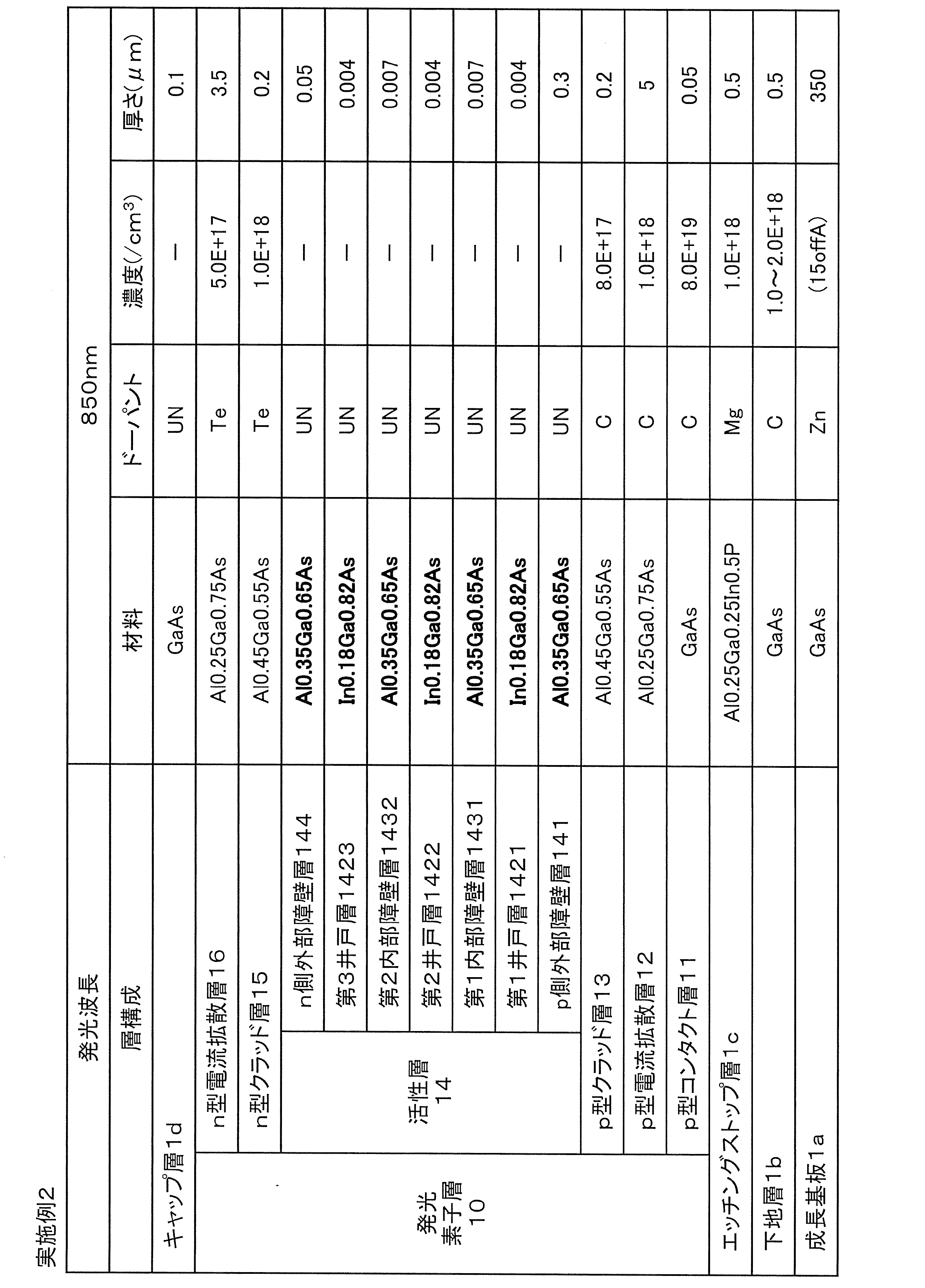
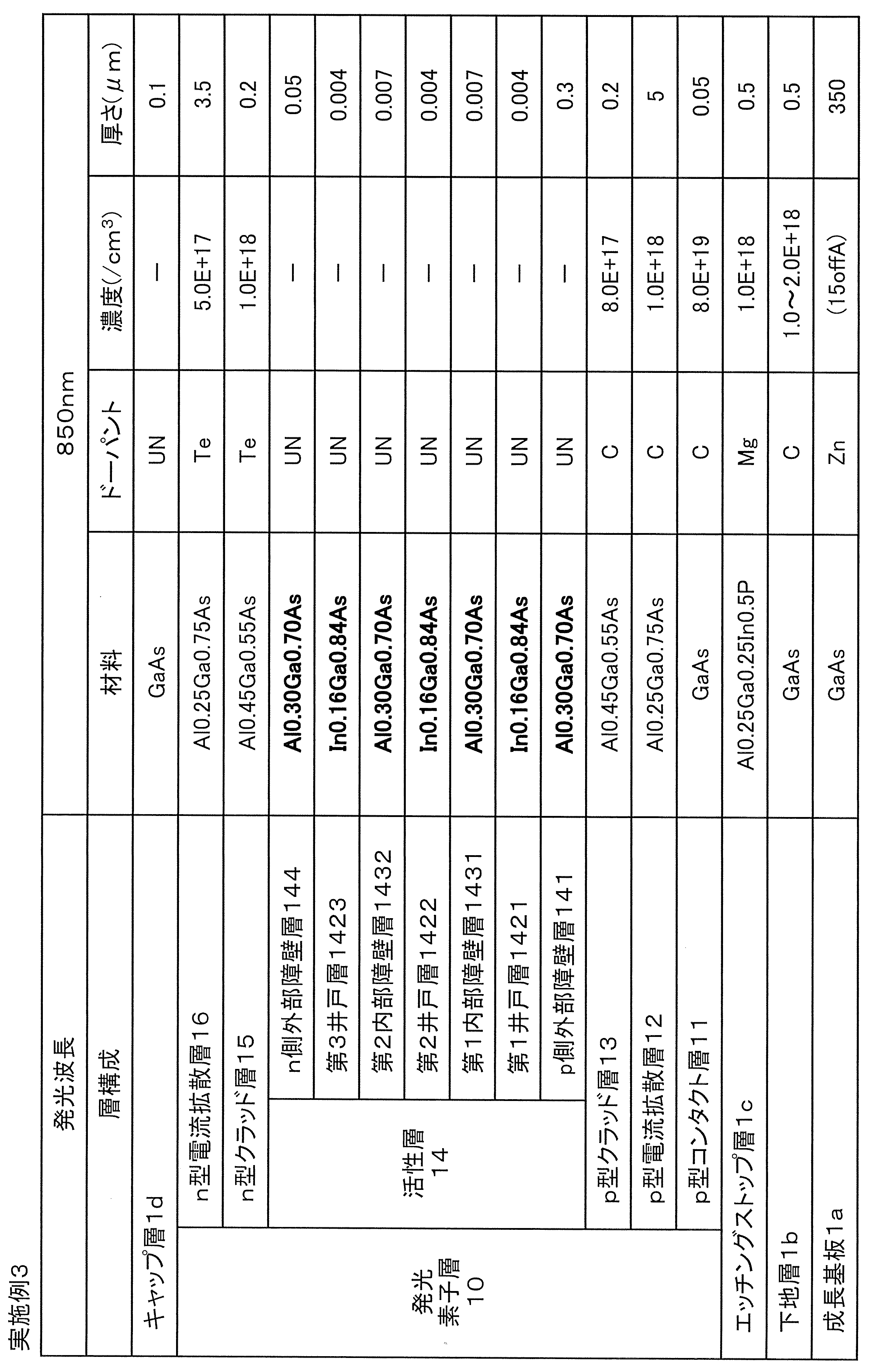
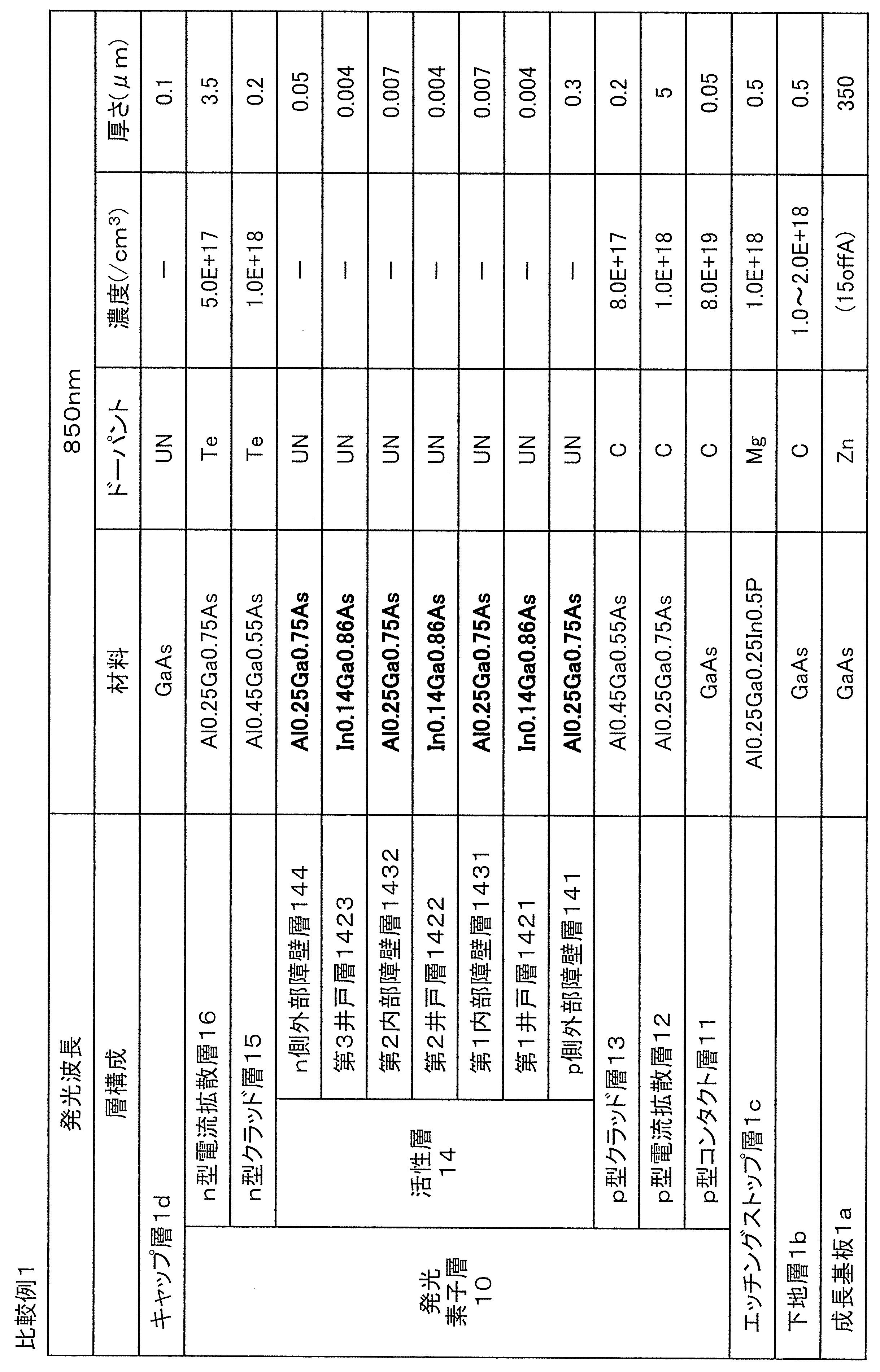
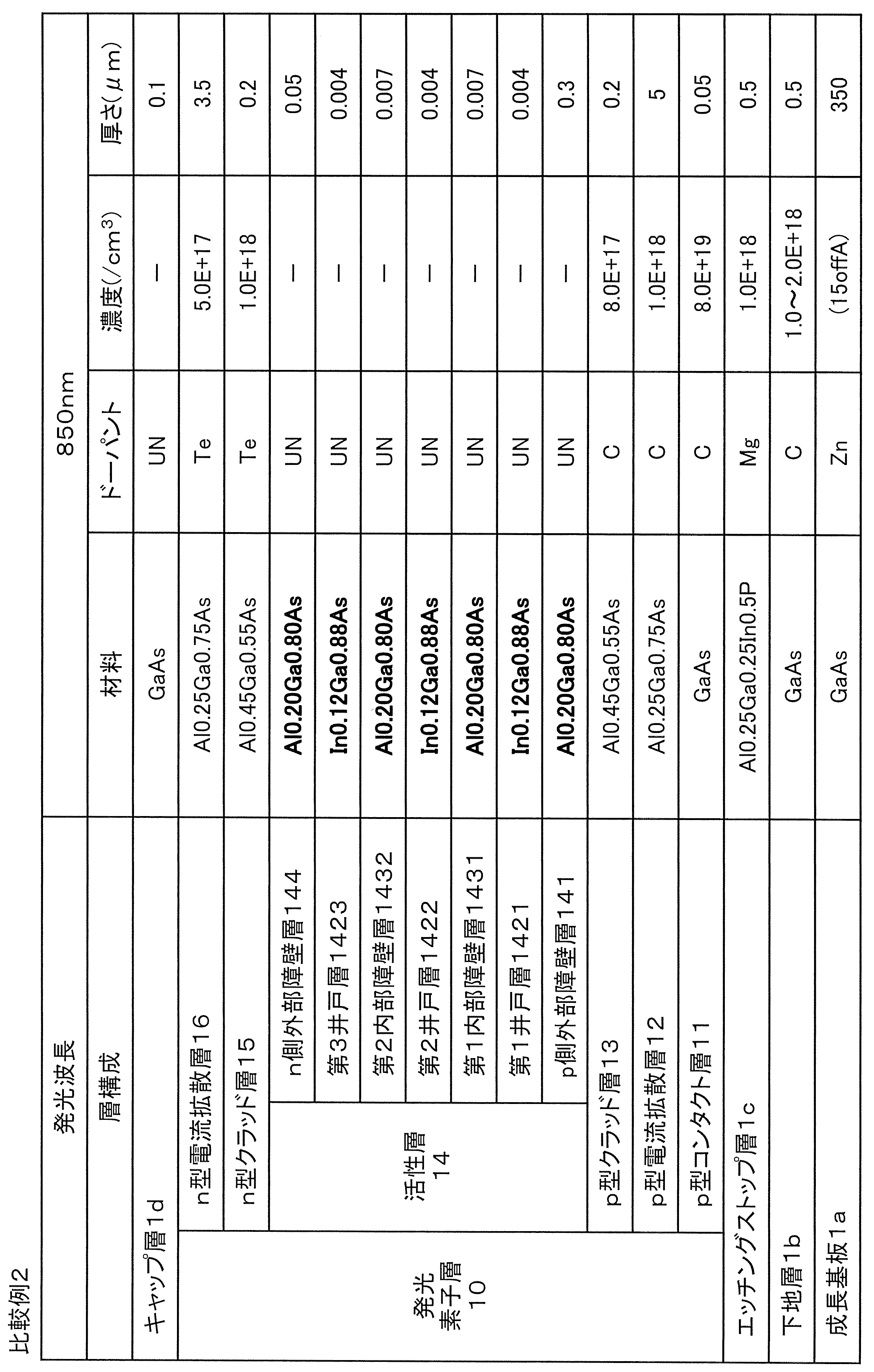

<実施例1の半導体層形成基板>
では、表1を参照しつつ、実施例1の半導体層形成基板1について説明を行う。
では、表1を参照しつつ、実施例1の半導体層形成基板1について説明を行う。
[成長基板]
成長基板1aには、p型不純物であるZn(亜鉛)を添加した、GaAs単結晶からなるウエハを用いた。そして、成長基板1aの厚さは350(μm)とし、成長基板1aにおける結晶成長面のオフ角は15°(表1には「15offA」と表記、以下同様)とした。
成長基板1aには、p型不純物であるZn(亜鉛)を添加した、GaAs単結晶からなるウエハを用いた。そして、成長基板1aの厚さは350(μm)とし、成長基板1aにおける結晶成長面のオフ角は15°(表1には「15offA」と表記、以下同様)とした。
[下地層]
下地層1bには、GaAsを用いた。下地層1bには、p型不純物であるC(炭素)を、1.0×10¹⁸~2.0×10¹⁸(表1には「1.0~2.0E+18」と表記、以下同様)の濃度となるように添加した。下地層1bの厚さは0.5(μm)とした。
下地層1bには、GaAsを用いた。下地層1bには、p型不純物であるC(炭素)を、1.0×10¹⁸~2.0×10¹⁸(表1には「1.0~2.0E+18」と表記、以下同様)の濃度となるように添加した。下地層1bの厚さは0.5(μm)とした。
[エッチングストップ層]
エッチングストップ層1cには、Al0.25Ga0.25In0.5P(表1には「Al0.25Ga0.25In0.5P」と表記、以下同様)を用いた。エッチングストップ層1cには、p型不純物であるMg(マグネシウム)を、1.0×10¹⁸の濃度となるように添加した。エッチングストップ層1cの厚さは0.5(μm)とした。
エッチングストップ層1cには、Al0.25Ga0.25In0.5P(表1には「Al0.25Ga0.25In0.5P」と表記、以下同様)を用いた。エッチングストップ層1cには、p型不純物であるMg(マグネシウム)を、1.0×10¹⁸の濃度となるように添加した。エッチングストップ層1cの厚さは0.5(μm)とした。
[発光素子層]
発光素子層10の構成は以下の通りである。なお、ここでは、発光素子層10(より具体的には活性層14)の発光波長(設計値)を850nmとした。
発光素子層10の構成は以下の通りである。なお、ここでは、発光素子層10(より具体的には活性層14)の発光波長(設計値)を850nmとした。
(p型コンタクト層)
p型コンタクト層11には、GaAsを用いた。p型コンタクト層11には、p型不純物であるCを、8.0×10¹⁹の濃度となるように添加した。p型コンタクト層11の厚さは0.05(μm)とした。
p型コンタクト層11には、GaAsを用いた。p型コンタクト層11には、p型不純物であるCを、8.0×10¹⁹の濃度となるように添加した。p型コンタクト層11の厚さは0.05(μm)とした。
(p型電流拡散層)
p型電流拡散層12には、Al0.25Ga0.75Asを用いた。p型電流拡散層12には、p型不純物であるCを、1.0×10¹⁸の濃度となるように添加した。p型電流拡散層12の厚さは5(μm)とした。
p型電流拡散層12には、Al0.25Ga0.75Asを用いた。p型電流拡散層12には、p型不純物であるCを、1.0×10¹⁸の濃度となるように添加した。p型電流拡散層12の厚さは5(μm)とした。
(p型クラッド層)
p型クラッド層13には、Al0.45Ga0.55Asを用いた。p型クラッド層13には、p型不純物であるCを、8.0×10¹⁷の濃度となるように添加した。p型クラッド層13の厚さは0.2(μm)とした。
p型クラッド層13には、Al0.45Ga0.55Asを用いた。p型クラッド層13には、p型不純物であるCを、8.0×10¹⁷の濃度となるように添加した。p型クラッド層13の厚さは0.2(μm)とした。
(活性層)
活性層14の構成は以下の通りである。
活性層14の構成は以下の通りである。
〔p側外部障壁層〕
p側外部障壁層141には、Al0.45Ga0.55Asを用いた。p側外部障壁層141には、p型不純物およびn型不純物を添加していない(アンドープ(表1には「UN」と表記、以下同様))。p側外部障壁層141の厚さは0.3(μm)とした。
p側外部障壁層141には、Al0.45Ga0.55Asを用いた。p側外部障壁層141には、p型不純物およびn型不純物を添加していない(アンドープ(表1には「UN」と表記、以下同様))。p側外部障壁層141の厚さは0.3(μm)とした。
〔第1井戸層〕
第1井戸層1421には、In0.19Ga0.81Asを用いた。第1井戸層1421には、p型不純物およびn型不純物を添加していない。第1井戸層1421の厚さは0.004(μm)とした。
第1井戸層1421には、In0.19Ga0.81Asを用いた。第1井戸層1421には、p型不純物およびn型不純物を添加していない。第1井戸層1421の厚さは0.004(μm)とした。
〔第1内部障壁層〕
第1内部障壁層1431には、Al0.45Ga0.55Asを用いた。第1内部障壁層1431には、p型不純物およびn型不純物を添加していない。第1内部障壁層1431の厚さは0.007(μm)とした。
第1内部障壁層1431には、Al0.45Ga0.55Asを用いた。第1内部障壁層1431には、p型不純物およびn型不純物を添加していない。第1内部障壁層1431の厚さは0.007(μm)とした。
〔第2井戸層〕
第2井戸層1422には、In0.19Ga0.81Asを用いた。第2井戸層1422には、p型不純物およびn型不純物を添加していない。第2井戸層1422の厚さは0.004(μm)とした。
第2井戸層1422には、In0.19Ga0.81Asを用いた。第2井戸層1422には、p型不純物およびn型不純物を添加していない。第2井戸層1422の厚さは0.004(μm)とした。
〔第2内部障壁層〕
第2内部障壁層1432には、Al0.45Ga0.55Asを用いた。第2内部障壁層1432には、p型不純物およびn型不純物を添加していない。第2内部障壁層1432の厚さは0.007(μm)とした。
第2内部障壁層1432には、Al0.45Ga0.55Asを用いた。第2内部障壁層1432には、p型不純物およびn型不純物を添加していない。第2内部障壁層1432の厚さは0.007(μm)とした。
〔第3井戸層〕
第3井戸層1423には、In0.19Ga0.81Asを用いた。第3井戸層1423には、p型不純物およびn型不純物を添加していない。第3井戸層1423の厚さは0.004(μm)とした。
第3井戸層1423には、In0.19Ga0.81Asを用いた。第3井戸層1423には、p型不純物およびn型不純物を添加していない。第3井戸層1423の厚さは0.004(μm)とした。
〔n側外部障壁層〕
n側外部障壁層144には、Al0.45Ga0.55Asを用いた。n側外部障壁層144には、p型不純物およびn型不純物を添加していない。n側外部障壁層144の厚さは0.05(μm)とした。
n側外部障壁層144には、Al0.45Ga0.55Asを用いた。n側外部障壁層144には、p型不純物およびn型不純物を添加していない。n側外部障壁層144の厚さは0.05(μm)とした。
(n型クラッド層)
n型クラッド層15には、Al0.45Ga0.55Asを用いた。n型クラッド層15には、n型不純物であるTe(テルル)を、1.0×10¹⁸の濃度となるように添加した。n型クラッド層15の厚さは0.2(μm)とした。
n型クラッド層15には、Al0.45Ga0.55Asを用いた。n型クラッド層15には、n型不純物であるTe(テルル)を、1.0×10¹⁸の濃度となるように添加した。n型クラッド層15の厚さは0.2(μm)とした。
(n型電流拡散層)
n型電流拡散層16には、Al0.25Ga0.75Asを用いた。n型電流拡散層16には、n型不純物であるTeを、5.0×10¹⁷の濃度となるように添加した。n型電流拡散層16の厚さは3.5(μm)とした。
n型電流拡散層16には、Al0.25Ga0.75Asを用いた。n型電流拡散層16には、n型不純物であるTeを、5.0×10¹⁷の濃度となるように添加した。n型電流拡散層16の厚さは3.5(μm)とした。
[キャップ層]
キャップ層1dには、GaAsを用いた。キャップ層1dには、p型不純物およびn型不純物を添加していない。キャップ層1dの厚さは0.1(μm)とした。
キャップ層1dには、GaAsを用いた。キャップ層1dには、p型不純物およびn型不純物を添加していない。キャップ層1dの厚さは0.1(μm)とした。
<実施例2の半導体層形成基板>
次に、表2を参照しつつ、実施例2の半導体層形成基板1について説明を行う。
実施例2の半導体層形成基板1は、活性層14を構成する各層の構成材料を除けば、実施例1の半導体層形成基板1と同様の構成を有している。
ここで、実施例2の半導体層形成基板1では、活性層14を構成する障壁層(p側外部障壁層141、第1内部障壁層1431、第2内部障壁層1432およびn側外部障壁層144)に、実施例1よりもAlの比率が低い(Gaの比率が高い)、Al0.35Ga0.65Asを用いた。また、実施例2の半導体層形成基板1では、活性層14を構成する井戸層142(第1井戸層1421~第3井戸層1423)に、実施例1よりもInの比率が低い(Gaの比率が高い)、In0.18Ga0.82Asを用いた。
次に、表2を参照しつつ、実施例2の半導体層形成基板1について説明を行う。
実施例2の半導体層形成基板1は、活性層14を構成する各層の構成材料を除けば、実施例1の半導体層形成基板1と同様の構成を有している。
ここで、実施例2の半導体層形成基板1では、活性層14を構成する障壁層(p側外部障壁層141、第1内部障壁層1431、第2内部障壁層1432およびn側外部障壁層144)に、実施例1よりもAlの比率が低い(Gaの比率が高い)、Al0.35Ga0.65Asを用いた。また、実施例2の半導体層形成基板1では、活性層14を構成する井戸層142(第1井戸層1421~第3井戸層1423)に、実施例1よりもInの比率が低い(Gaの比率が高い)、In0.18Ga0.82Asを用いた。
<実施例3の半導体層形成基板>
続いて、表3を参照しつつ、実施例3の半導体層形成基板1について説明を行う。
実施例3の半導体層形成基板1は、活性層14を構成する各層の構成材料を除けば、実施例1、2の半導体層形成基板1と同様の構成を有している。
ここで、実施例3の半導体層形成基板1では、活性層14を構成する障壁層(p側外部障壁層141、第1内部障壁層1431、第2内部障壁層1432およびn側外部障壁層144)に、実施例2よりもAlの比率が低い(Gaの比率が高い)、Al0.30Ga0.70Asを用いた。また、実施例3の半導体層形成基板1では、活性層14を構成する井戸層142(第1井戸層1421~第3井戸層1423)に、実施例2よりもInの比率が低い(Gaの比率が高い)、In0.16Ga0.84Asを用いた。
続いて、表3を参照しつつ、実施例3の半導体層形成基板1について説明を行う。
実施例3の半導体層形成基板1は、活性層14を構成する各層の構成材料を除けば、実施例1、2の半導体層形成基板1と同様の構成を有している。
ここで、実施例3の半導体層形成基板1では、活性層14を構成する障壁層(p側外部障壁層141、第1内部障壁層1431、第2内部障壁層1432およびn側外部障壁層144)に、実施例2よりもAlの比率が低い(Gaの比率が高い)、Al0.30Ga0.70Asを用いた。また、実施例3の半導体層形成基板1では、活性層14を構成する井戸層142(第1井戸層1421~第3井戸層1423)に、実施例2よりもInの比率が低い(Gaの比率が高い)、In0.16Ga0.84Asを用いた。
<比較例1の半導体層形成基板>
さらに、表4を参照しつつ、比較例1の半導体層形成基板1について説明を行う。
比較例1の半導体層形成基板1は、活性層14を構成する各層の構成材料を除けば、実施例1~3の半導体層形成基板1と同様の構成を有している。
ここで、比較例1の半導体層形成基板1では、活性層14を構成する障壁層(p側外部障壁層141、第1内部障壁層1431、第2内部障壁層1432およびn側外部障壁層144)に、実施例3よりもAlの比率が低い(Gaの比率が高い)、Al0.25Ga0.75Asを用いた。また、比較例1の半導体層形成基板1では、活性層14を構成する井戸層142(第1井戸層1421~第3井戸層1423)に、実施例3よりもInの比率が低い(Gaの比率が高い)、In0.14Ga0.86Asを用いた。
さらに、表4を参照しつつ、比較例1の半導体層形成基板1について説明を行う。
比較例1の半導体層形成基板1は、活性層14を構成する各層の構成材料を除けば、実施例1~3の半導体層形成基板1と同様の構成を有している。
ここで、比較例1の半導体層形成基板1では、活性層14を構成する障壁層(p側外部障壁層141、第1内部障壁層1431、第2内部障壁層1432およびn側外部障壁層144)に、実施例3よりもAlの比率が低い(Gaの比率が高い)、Al0.25Ga0.75Asを用いた。また、比較例1の半導体層形成基板1では、活性層14を構成する井戸層142(第1井戸層1421~第3井戸層1423)に、実施例3よりもInの比率が低い(Gaの比率が高い)、In0.14Ga0.86Asを用いた。
<比較例2の半導体層形成基板>
次いで、表5を参照しつつ、比較例2の半導体層形成基板1について説明を行う。
比較例2の半導体層形成基板1は、活性層14を構成する各層の構成材料を除けば、実施例1~3および比較例1の半導体層形成基板1と同様の構成を有している。
ここで、比較例2の半導体層形成基板1では、活性層14を構成する障壁層(p側外部障壁層141、第1内部障壁層1431、第2内部障壁層1432およびn側外部障壁層144)に、比較例1よりもAlの比率が低い(Gaの比率が高い)、Al0.20Ga0.80Asを用いた。また、比較例2の半導体層形成基板1では、活性層14を構成する井戸層142(第1井戸層1421~第3井戸層1423)に、比較例1よりもInの比率が低い(Gaの比率が高い)、In0.12Ga0.88Asを用いた。
次いで、表5を参照しつつ、比較例2の半導体層形成基板1について説明を行う。
比較例2の半導体層形成基板1は、活性層14を構成する各層の構成材料を除けば、実施例1~3および比較例1の半導体層形成基板1と同様の構成を有している。
ここで、比較例2の半導体層形成基板1では、活性層14を構成する障壁層(p側外部障壁層141、第1内部障壁層1431、第2内部障壁層1432およびn側外部障壁層144)に、比較例1よりもAlの比率が低い(Gaの比率が高い)、Al0.20Ga0.80Asを用いた。また、比較例2の半導体層形成基板1では、活性層14を構成する井戸層142(第1井戸層1421~第3井戸層1423)に、比較例1よりもInの比率が低い(Gaの比率が高い)、In0.12Ga0.88Asを用いた。
<比較例3の半導体層形成基板>
最後に、表6を参照しつつ、比較例3の半導体層形成基板1について説明を行う。
比較例3の半導体層形成基板1は、活性層14を構成する各層の構成材料を除けば、実施例1~3および比較例1、2の半導体層形成基板1と同様の構成を有している。
ここで、比較例3の半導体層形成基板1では、活性層14を構成する障壁層(p側外部障壁層141、第1内部障壁層1431、第2内部障壁層1432およびn側外部障壁層144)に、比較例2よりもAlの比率が低い(Gaの比率が高い)、Al0.15Ga0.85Asを用いた。また、比較例3の半導体層形成基板1では、活性層14を構成する井戸層142(第1井戸層1421~第3井戸層1423)に、比較例2よりもInの比率が低い(Gaの比率が高い)、In0.11Ga0.89Asを用いた。
最後に、表6を参照しつつ、比較例3の半導体層形成基板1について説明を行う。
比較例3の半導体層形成基板1は、活性層14を構成する各層の構成材料を除けば、実施例1~3および比較例1、2の半導体層形成基板1と同様の構成を有している。
ここで、比較例3の半導体層形成基板1では、活性層14を構成する障壁層(p側外部障壁層141、第1内部障壁層1431、第2内部障壁層1432およびn側外部障壁層144)に、比較例2よりもAlの比率が低い(Gaの比率が高い)、Al0.15Ga0.85Asを用いた。また、比較例3の半導体層形成基板1では、活性層14を構成する井戸層142(第1井戸層1421~第3井戸層1423)に、比較例2よりもInの比率が低い(Gaの比率が高い)、In0.11Ga0.89Asを用いた。
なお、実施例1~3および比較例1~3で、井戸層142(第1井戸層1421~第3井戸層1423)におけるInおよびGaの組成が異なっているのは、それぞれの発光波長を、850(nm)に揃えるためである。
<各実施例および各比較例の半導体層形成基板の関係>
表7は、各実施例および各比較例の半導体層形成基板1における、活性層14の物理的な特性を示している。より具体的に説明すると、表7は、各半導体層形成基板1における、障壁層(AlbGa1-bAs)のAl組成比bと、障壁層のバンドギャップEgB(eV)と、井戸層142(InaGa1-aAs)のIn組成比aと、井戸層142のバンドギャップEgW(eV)と、障壁層と井戸層142とのバンドギャップ差ΔE(=EgB-EgW)との関係を示している。
表7は、各実施例および各比較例の半導体層形成基板1における、活性層14の物理的な特性を示している。より具体的に説明すると、表7は、各半導体層形成基板1における、障壁層(AlbGa1-bAs)のAl組成比bと、障壁層のバンドギャップEgB(eV)と、井戸層142(InaGa1-aAs)のIn組成比aと、井戸層142のバンドギャップEgW(eV)と、障壁層と井戸層142とのバンドギャップ差ΔE(=EgB-EgW)との関係を示している。

まず、表7より、比較例3、比較例2、比較例1、実施例3、実施例2、実施例1の順で、障壁層のAl組成比bが大きくなっていく(Alの比率が上がり、Gaの比率が下がる)ことがわかる。
また、表7より、障壁層のAl組成比bが増加するほど、障壁層のバンドギャップEgBが増大していくことがわかる。なお、表7に(参考)として示したように、b=1とした場合、すなわち、障壁層をAlAsで構成した場合、障壁層のバンドギャップEgBは2.17(eV)となる。
さらに、表7より、井戸層142のIn組成比aが増加するほど、井戸層142のバンドギャップEgWが減少していくことがわかる。なお、表7に(参考)として示したように、a=0.2とした場合、すなわち、井戸層142をIn0.2Ga0.8Asで構成した場合、井戸層のバンドギャップEgWは1.14(eV)となる。
そして、この例においては、比較例3、比較例2、比較例1、実施例3、実施例2、実施例1の順で、障壁層のAl組成比bが増加(バンドギャップEgBが増大)し、且つ、井戸層142のIn組成比aが増加(バンドギャップEgWが減少)している。その結果、表7に示したように、比較例3、比較例2、比較例1、実施例3、実施例2、実施例1の順で、バンドギャップ差ΔEが増加している。なお、表7に(参考)として示したように、障壁層をAlAsで構成し、且つ、井戸層142をIn0.2Ga0.8Asで構成した場合、バンドギャップ差ΔEは1.03(eV)となる。
<半導体発光素子>
このようにして得られた実施例1~3および比較例1~3の半導体層形成基板1を出発材料とし、図6に示す製造方法を用いて、半導体発光素子2を作製した。そして、得られた各半導体発光素子2に対し、各種評価を行った。なお、今回は、実施例1~3および比較例1~3のそれぞれにおいて、評価用の試料を2個ずつ用意した。以下では、これらを、例えば実施例1(1)、実施例1(2)と表記することがある。
このようにして得られた実施例1~3および比較例1~3の半導体層形成基板1を出発材料とし、図6に示す製造方法を用いて、半導体発光素子2を作製した。そして、得られた各半導体発光素子2に対し、各種評価を行った。なお、今回は、実施例1~3および比較例1~3のそれぞれにおいて、評価用の試料を2個ずつ用意した。以下では、これらを、例えば実施例1(1)、実施例1(2)と表記することがある。
<評価>
今回は、各半導体発光素子2の順方向電流-発光出力の直線性と、各半導体発光素子2の入出力の応答性(立ち上がりおよび立ち下がり)とを用いて、各半導体発光素子2の評価を行った。
今回は、各半導体発光素子2の順方向電流-発光出力の直線性と、各半導体発光素子2の入出力の応答性(立ち上がりおよび立ち下がり)とを用いて、各半導体発光素子2の評価を行った。
[直線性]
直線性の評価は、次のようにして行った。まず、各半導体発光素子2に、順方向電流IFを0(mA)から10(mA)の範囲内で大きさを変えながら供給し、各半導体発光素子2からの発光出力Poを測定した。そして、得られた順方向電流-発光出力特性に基づき、2種類の規格化を行った。
直線性の評価は、次のようにして行った。まず、各半導体発光素子2に、順方向電流IFを0(mA)から10(mA)の範囲内で大きさを変えながら供給し、各半導体発光素子2からの発光出力Poを測定した。そして、得られた順方向電流-発光出力特性に基づき、2種類の規格化を行った。
まず、1つ目は、順方向電流IF=10mAのときの発光効率を基準として、すべての発光効率を規格化したものである。以下ではこれを第1規格化発光効率Eff[IF/10]と呼ぶことにする。ここで、発光出力Poを順方向電流IFの値で割ったものを発光効率Effとした。例えば、順方向電流がIFmAのときの発光出力をPo(IF)とすると、順方向電流がIFmAのときの発光効率はEff(IF)=Po(IF)/IFで表される。さらに、第1規格化発光効率はEff[IF/10]=Eff(IF)/Eff(10)で表される。
また、2つ目は、順方向電流IF=5mAのときの発光効率を基準として、すべての発光効率を規格化したものである。以下ではこれを第2規格化発光効率Eff[IF/5]と呼ぶことにする。
また、2つ目は、順方向電流IF=5mAのときの発光効率を基準として、すべての発光効率を規格化したものである。以下ではこれを第2規格化発光効率Eff[IF/5]と呼ぶことにする。
図7は、各実施例および各比較例の、順方向電流IFと第1規格化発光効率Eff[IF/10]との関係を示すグラフ図である。図7において、横軸は順方向電流IF(mA)であり、縦軸は第1規格化発光効率Eff[IF/10]である。
図8は、各実施例および各比較例の、順方向電流IFと第2規格化発光効率Eff[IF/5]との関係を示すグラフ図である。図8において、横軸は順方向電流IF(mA)であり、縦軸は第2規格化発光効率Eff[IF/5]である。
したがって、図7および図8においては、それぞれの縦軸の数値が1に近いほど、基準となる順方向電流IFに対する発光出力Poの直線性が高い(リニアリティがよい)、ということになる。
図7および図8より、実施例1~実施例3および比較例1~比較例3では、順方向電流IF≦2(mA)となる低電流域において、順方向電流IFの値が小さくなるほど、縦軸の数値が減少していく傾向がみられた。ただし、順方向電流IF=0(mA)~10(mA)の範囲において、実施例1~実施例3の縦軸の数値は、比較例1~比較例3の縦軸の数値よりも大きくなっていた。
ここで、図7に示す例において、順方向電流IF=1(mA)の場合、比較例1~比較例3では、縦軸の数値が1未満(0.9の近傍)となっていたのに対し、実施例1~実施例3では、縦軸の数値が1以上となっていた。また、図8に示す例において、順方向電流IF=1(mA)の場合、比較例1~比較例3では、縦軸の数値が1未満(0.8の近傍)となっていたのに対し、実施例1~実施例3では、縦軸の数値が1の近傍となっていた。
表8は、各実施例および各比較例の半導体発光素子2における、障壁層の組成と、井戸層142の組成と、バンドギャップ差ΔEと、順方向電流IF=1(mA)のときの第1規格化発光効率Eff[1/10]と、順方向電流IF=1(mA)のときの第2規格化発光効率Eff[1/5]との関係を示している。

(第1規格化発光効率)
最初に、第1規格化発光効率Eff[1/10]について説明を行う。
まず、表8より、比較例3、比較例2、比較例1、実施例3、実施例2、実施例1の順で、第1規格化発光効率Eff[1/10]が大きくなっていることがわかる。これは、換言すれば、活性層14における障壁層と井戸層142とのバンドギャップ差ΔEが大きくなるほど、第1規格化発光効率Eff[1/10]が高くなることを意味している。
最初に、第1規格化発光効率Eff[1/10]について説明を行う。
まず、表8より、比較例3、比較例2、比較例1、実施例3、実施例2、実施例1の順で、第1規格化発光効率Eff[1/10]が大きくなっていることがわかる。これは、換言すれば、活性層14における障壁層と井戸層142とのバンドギャップ差ΔEが大きくなるほど、第1規格化発光効率Eff[1/10]が高くなることを意味している。
ここで、バンドギャップ差ΔEが0.60(eV)以上となる実施例1~実施例3の場合、第1規格化発光効率Eff[1/10]は、1.00~1.12となる。これに対し、バンドギャップ差ΔEが0.50(eV)以下となる比較例1~比較例3の場合、第1規格化発光効率Eff[1/10]は、0.85~0.91となる。ここで、第1規格化発光効率Eff[1/10]の値が1の場合、順方向電流IF=1mAのときの発光効率と順方向電流IF=10mAのときの発光効率とが等しいことになる。また、第1規格化発光効率Eff[1/10]の値が1よりも大きい場合、順方向電流IF=1mAのときの発光効率が順方向電流IF=10mAのときの発光効率よりも高いことになる。したがって、実施例1~実施例3は、比較例1~比較例3と比べて、低電流域における発光効率が向上しているということができる。また、実施例1~実施例3を比較すると、バンドギャップ差ΔEが最も大きい実施例1は、バンドギャップ差ΔEが最も小さい実施例3よりも、低電流域における発光効率が向上しているということができる。
(第2規格化発光効率)
次に、第2規格化発光効率Eff[1/5]について説明を行う。
まず、表8より、比較例3、比較例2、比較例1、実施例3、実施例2、実施例1の順で、第2規格化発光効率Eff[1/5]が大きくなっていることがわかる。これは、換言すれば、活性層14における障壁層と井戸層142とのバンドギャップ差ΔEが大きくなるほど、第2規格化発光効率Eff[1/5]が高くなることを意味している。
次に、第2規格化発光効率Eff[1/5]について説明を行う。
まず、表8より、比較例3、比較例2、比較例1、実施例3、実施例2、実施例1の順で、第2規格化発光効率Eff[1/5]が大きくなっていることがわかる。これは、換言すれば、活性層14における障壁層と井戸層142とのバンドギャップ差ΔEが大きくなるほど、第2規格化発光効率Eff[1/5]が高くなることを意味している。
ここで、バンドギャップ差ΔEが0.60(eV)以上となる実施例1~実施例3の場合、第2規格化発光効率Eff[1/5]は、0.97~1.05となる。これに対し、バンドギャップ差ΔEが0.50(eV)以下となる比較例1~比較例3の場合、第2規格化発光効率Eff[1/5]は、0.85~0.89となる。これらより、実施例1~実施例3は、比較例1~比較例3と比べて、第2規格化発光効率Eff[1/5]の値が1に近くなるといえる。したがって、実施例1~実施例3は、比較例1~比較例3と比べて、低電流域における発光効率が向上しているということができる。また、実施例1~実施例3を比較すると、バンドギャップ差ΔEが最も大きい実施例1は、バンドギャップ差ΔEが最も小さい実施例3よりも、低電流域における発光効率が向上しているということができる。
(多重量子井戸構造におけるバンド構造)
ここで、各実施例の半導体発光素子2が、各比較例の半導体発光素子2よりも、低電流域における直線性が高くなった理由について考察する。
図9(a)、(b)は、比較例および実施例にかかる半導体発光素子2の、多重量子井戸構造におけるバンド構造を模式的に示す図である。
ここで、各実施例の半導体発光素子2が、各比較例の半導体発光素子2よりも、低電流域における直線性が高くなった理由について考察する。
図9(a)、(b)は、比較例および実施例にかかる半導体発光素子2の、多重量子井戸構造におけるバンド構造を模式的に示す図である。
図9(a)、(b)のそれぞれは、2つの障壁層およびこれら2つの障壁層に挟まれた井戸層と、各層のバンドギャップとの関係を示している。なお、ここでは、図9(a)、(b)のそれぞれにおける井戸層のバンドギャップは同じで、図9(a)における障壁層のバンドギャップよりも、図9(b)における障壁層のバンドギャップが大きい場合を例としている。そして、図9(a)における障壁層と井戸層とのバンドギャップ差ΔEを第1バンドギャップ差ΔE1と呼ぶことにし、図9(b)における障壁層と井戸層とのバンドギャップ差ΔEを第2バンドギャップ差ΔE2と呼ぶことにする。
活性層14を多重量子井戸構造で構成した場合、通電に伴い、一方(図中左側)の障壁層から井戸層に電子が注入され、他方(図中右側)の障壁層からこの井戸層に正孔が注入される。以下では、これら電子および正孔を、まとめてキャリアと称することがある。このようにして井戸層に注入された電子および正孔は、この井戸層を挟む2つの障壁層によって井戸層内に閉じ込められる。そして、井戸層内に閉じ込められた電子および正孔は、両者が直接結合することによって発光に寄与する発光再結合を行い、また、両者が井戸層内に存在する欠陥準位に捕獲されることによって発光に寄与せずに熱となる非発光再結合を行う。
ここで、図9(a)に示すようにバンドギャップ差ΔEが相対的に小さい第1バンドギャップ差ΔE1の場合、井戸層内にキャリアを閉じ込める力が小さくなる。このため、井戸層内でキャリアが不安定となりやすく、キャリアが欠陥準位に捕獲される非発光再結合が起きやすい。したがって、この場合は、発光再結合に対する非発光再結合の比率が高くなることから、発光効率が低下しやすくなると考えられる。
一方、図9(b)に示すようにバンドギャップ差ΔEが相対的に大きい第2バンドギャップ差ΔE2の場合、井戸層内にキャリアを閉じ込める力が大きくなる。このため、井戸層内でキャリアが安定となりやすく、キャリアが欠陥準位に捕獲される非発光再結合が起きにくい。したがって、この場合は、発光再結合に対する非発光再結合の比率が低くなることから、発光効率が向上しやすくなると考えられる。
そして、上述した各実施例および各比較例の直線性の評価結果から、バンドギャップ差ΔEが0.50(eV)以下となる場合(比較例1~比較例3)が、図9(a)に示す例に対応しているものと考えられる。また、バンドギャップ差ΔEが0.60(eV)以上となる場合(実施例1~実施例3)が、図9(b)に示す例に対応しているものと考えられる。
[応答性]
応答性の評価は、次のようにして行った。まず、各半導体発光素子2に、電流値30mA、パルス幅5μsの順方向電流IFを供給し、各半導体発光素子2からの発光出力Poを測定した。そして、順方向電流IF(パルス電流)の立ち上がりにおいて、発光出力Poのピーク値の10%から90%になるまでの時間を、立ち上がり時間Tr(nsec)とした。また、順方向電流IF(パルス電流)の立ち下がりにおいて、発光出力Poのピーク値の90%から10%になるまでの時間を、立ち下がり時間Tf(nsec)とした。
応答性の評価は、次のようにして行った。まず、各半導体発光素子2に、電流値30mA、パルス幅5μsの順方向電流IFを供給し、各半導体発光素子2からの発光出力Poを測定した。そして、順方向電流IF(パルス電流)の立ち上がりにおいて、発光出力Poのピーク値の10%から90%になるまでの時間を、立ち上がり時間Tr(nsec)とした。また、順方向電流IF(パルス電流)の立ち下がりにおいて、発光出力Poのピーク値の90%から10%になるまでの時間を、立ち下がり時間Tf(nsec)とした。
図10は、各実施例および各比較例にかかる半導体発光素子2の、応答時間(立ち上がり時間Trおよび立ち下がり時間Tf)を示すグラフ図である。図10において、横軸は各実施例および各比較例を並べたものであり、縦軸は応答時間(ns)である。
表9は、各実施例および各比較例の半導体発光素子2における、障壁層の組成と、井戸層142の組成と、バンドギャップ差ΔEと、立ち上がり時間Trと、立ち下がり時間Tfとの関係を示している。

(立ち上がり時間)
最初に、立ち上がり時間Trについて説明を行う。
バンドギャップ差ΔEが0.60(eV)以上となる実施例1~3では、立ち上がり時間Trが8.36(nsec)~9.02(nsec)であった。これに対し、バンドギャップ差ΔEが0.50(eV)以下となる比較例1~3では、立ち上がり時間Trが9.30(nsec)~10.04(nsec)であった。これらより、実施例1~3は、比較例1~3と比べて、立ち上がり時間Trが短くなっているといえる。したがって、実施例1~実施例3は、比較例1~比較例3と比べて、立ち上がりの応答性が向上しているということができる。また、実施例1~実施例3を比較すると、バンドギャップ差ΔEが最も大きい実施例1は、バンドギャップ差ΔEが最も小さい実施例3よりも、立ち上がりの応答性が向上しているということができる。
最初に、立ち上がり時間Trについて説明を行う。
バンドギャップ差ΔEが0.60(eV)以上となる実施例1~3では、立ち上がり時間Trが8.36(nsec)~9.02(nsec)であった。これに対し、バンドギャップ差ΔEが0.50(eV)以下となる比較例1~3では、立ち上がり時間Trが9.30(nsec)~10.04(nsec)であった。これらより、実施例1~3は、比較例1~3と比べて、立ち上がり時間Trが短くなっているといえる。したがって、実施例1~実施例3は、比較例1~比較例3と比べて、立ち上がりの応答性が向上しているということができる。また、実施例1~実施例3を比較すると、バンドギャップ差ΔEが最も大きい実施例1は、バンドギャップ差ΔEが最も小さい実施例3よりも、立ち上がりの応答性が向上しているということができる。
(立ち下がり時間)
次に、立ち下がり時間Tfについて説明を行う。
バンドギャップ差ΔEが0.60(eV)以上となる実施例1~3では、立ち下がり時間Tfが6.30(nsec)~6.50(nsec)であった。これに対し、バンドギャップ差ΔEが0.50(eV)以下となる比較例1~3では、立ち下がり時間Tfが6.54(nsec)~6.74(nsec)であった。これらより、実施例1~3は、比較例1~3に比べて、立ち下がり時間Tfが短くなっているといえる。したがって、実施例1~3は、比較例1~3に比べて、立ち下がりの応答性が向上しているということができる。また、実施例1~実施例3を比較すると、バンドギャップ差ΔEが最も大きい実施例1は、バンドギャップ差ΔEが最も小さい実施例3よりも、立ち下がりの応答性が向上しているということができる。
次に、立ち下がり時間Tfについて説明を行う。
バンドギャップ差ΔEが0.60(eV)以上となる実施例1~3では、立ち下がり時間Tfが6.30(nsec)~6.50(nsec)であった。これに対し、バンドギャップ差ΔEが0.50(eV)以下となる比較例1~3では、立ち下がり時間Tfが6.54(nsec)~6.74(nsec)であった。これらより、実施例1~3は、比較例1~3に比べて、立ち下がり時間Tfが短くなっているといえる。したがって、実施例1~3は、比較例1~3に比べて、立ち下がりの応答性が向上しているということができる。また、実施例1~実施例3を比較すると、バンドギャップ差ΔEが最も大きい実施例1は、バンドギャップ差ΔEが最も小さい実施例3よりも、立ち下がりの応答性が向上しているということができる。
1…半導体層形成基板、2…半導体発光素子、3…半導体受光素子、4…発光素子側電極、5…受光素子側電極、6…レンズ、7…透明樹脂部、8…不透明樹脂部、10…発光素子層、11…p型コンタクト層、12…p型電流拡散層、13…p型クラッド層、14…活性層、141…p側外部障壁層、142…井戸層、143…内部障壁層、144…n側外部障壁層、15…n型クラッド層、16…n型電流拡散層、20…正電極部、30…負電極部、100…フォトカプラ
Claims (21)
- p型不純物を含む第1の半導体で構成されるp型半導体層と、
n型不純物を含む第2の半導体で構成されるn型半導体層と、
前記p型半導体層と前記n型半導体層との間に配置され、通電により発光する発光層とを有し、
前記発光層は、
InaGa1-aAs(0<a≦0.4)で構成された2層以上の井戸層と、
AlbGa1-bAs(0.3≦b≦0.45)で構成され、2層以上の前記井戸層のそれぞれを両側から挟み込む3層以上の障壁層と
を備える半導体発光素子。 - 前記発光層において、
それぞれの前記井戸層は、InaGa1-aAs(0.06≦a≦0.34)で構成され、
それぞれの前記障壁層は、AlbGa1-bAs(0.3≦b≦0.45)で構成されること
を特徴とする請求項1記載の半導体発光素子。 - 前記第1の半導体および前記第2の半導体が、ともにAlbGa1-bAsで構成されること
を特徴とする請求項1または2記載の半導体発光素子。 - p型不純物を含む第3の半導体で構成され、前記p型半導体層に供給する電流を拡散させるp型電流拡散層と、
n型不純物を含む第4の半導体で構成され、前記n型半導体層に供給する電流を拡散させるn型電流拡散層と
をさらに有し、
前記第3の半導体および前記第4の半導体が、ともにAlcGa1-cAs(c<b)で構成されること
を特徴とする請求項1乃至3のいずれか1項記載の半導体発光素子。 - 前記p型電流拡散層は前記p型半導体層よりも厚さが大きく、前記n型電流拡散層は前記n型半導体層よりも厚さが大きいこと
を特徴とする請求項4記載の半導体発光素子。 - 前記p型電流拡散層は、前記n型電流拡散層よりも厚さが大きいこと
を特徴とする請求項4または5記載の半導体発光素子。 - 前記p型電流拡散層におけるp型不純物の濃度が、前記n型電流拡散層におけるn型不純物の濃度よりも高いこと
を特徴とする請求項4乃至6のいずれか1項記載の半導体発光素子。 - 前記発光層を構成する前記井戸層および前記障壁層は、p型不純物およびn型不純物を含まないこと
を特徴とする請求項1乃至7のいずれか1項記載の半導体発光素子。 - 3層以上の前記障壁層は、
前記p型半導体層に最も近い側に配置されたp側障壁層と、
前記n型半導体層に最も近い側に配置されたn側障壁層と、
前記p側障壁層と前記n側障壁層との間に配置された1以上の内部障壁層と
を備えており、
前記p側障壁層および前記n側障壁層は、前記内部障壁層よりも厚さが大きいこと
を特徴とする請求項1乃至8のいずれか1項記載の半導体発光素子。 - 前記p側障壁層は、前記n側障壁層よりも厚さが大きいこと
を特徴とする請求項9記載の半導体発光素子。 - p型不純物を含む第1の半導体で構成されるp型半導体層と、
n型不純物を含む第2の半導体で構成されるn型半導体層と、
前記p型半導体層と前記n型半導体層との間に配置され、通電により発光する発光層とを有し、
前記発光層は、
第1のバンドギャップを有する第1の化合物半導体で構成された2層以上の井戸層と、
前記第1のバンドギャップとのバンドギャップ差が0.6eV以上となる第2のバンドギャップを有する第2の化合物半導体で構成され、2層以上の前記井戸層のそれぞれを両側から挟み込む3層以上の障壁層と
を備える半導体発光素子。 - 前記第1の化合物半導体および前記第2の化合物半導体が、ともにIII-V族半導体で構成されること
を特徴とする請求項11記載の半導体発光素子。 - 前記第1の化合物半導体および前記第2の化合物半導体は、ともにV族元素としてAsを含み且つPおよびNを含まないこと
を特徴とする請求項12記載の半導体発光素子。 - 前記第1の化合物半導体は、第1のIII族元素および第2のIII族元素を含むとともに、第3のIII族元素を含んでおらず、
前記第2の化合物半導体は、前記第2のIII族元素および前記第3のIII族元素を含むとともに、前記第1のIII族元素を含んでいないこと
を特徴とする請求項13記載の半導体発光素子。 - 前記第1のIII族元素はInであり、
前記第2のIII族元素はGaであり、
前記第3のIII族元素はAlであること
を特徴とする請求項14記載の半導体発光素子。 - 前記第1の半導体および前記第2の半導体が、ともにIII-V族半導体で構成されること
を特徴とする請求項11乃至15のいずれか1項記載の半導体発光素子。 - 前記第1の半導体および前記第2の半導体は、ともにV族元素としてAsを含み且つPおよびNを含まないこと
を特徴とする請求項16記載の半導体発光素子。 - 前記第1の半導体および前記第2の半導体は、ともにIII族元素としてGaおよびAlを含み且つInを含まないこと
を特徴とする請求項17記載の半導体発光素子。 - 前記第1の半導体、前記第2の半導体および前記第2の化合物半導体は、組成比が同じIII-V族半導体で構成されること
を特徴とする請求項11乃至16のいずれか1項記載の半導体発光素子。 - 通電により発光する発光素子と、
前記発光素子に対向して配置されるとともに、当該発光素子からの光を受光する受光素子とを含み、
前記発光素子は、
p型不純物を含む第1の半導体で構成されるp型半導体層と、
n型不純物を含む第2の半導体で構成されるn型半導体層と、
前記p型半導体層と前記n型半導体層との間に配置され、通電により発光する発光層とを有し、
前記発光層は、
InaGa1-aAs(0<a≦0.4)で構成された2層以上の井戸層と、
AlbGa1-bAs(0.3≦b≦0.45)で構成され、2層以上の前記井戸層のそれぞれを両側から挟み込む3層以上の障壁層と
を備える光伝達装置。 - 通電により発光する発光素子と、
前記発光素子に対向して配置されるとともに、当該発光素子からの光を受光する受光素子とを含み、
前記発光素子は、
p型不純物を含む第1の半導体で構成されるp型半導体層と、
n型不純物を含む第2の半導体で構成されるn型半導体層と、
前記p型半導体層と前記n型半導体層との間に配置され、通電により発光する発光層とを有し、
前記発光層は、
第1のバンドギャップを有する第1の化合物半導体で構成された2層以上の井戸層と、
前記第1のバンドギャップとのバンドギャップ差が0.6eV以上となる第2のバンドギャップを有する第2の化合物半導体で構成され、2層以上の前記井戸層のそれぞれを両側から挟み込む3層以上の障壁層と
を備える光伝達装置。
Priority Applications (1)
| Application Number | Priority Date | Filing Date | Title |
|---|---|---|---|
| JP2020535755A JPWO2020031954A1 (ja) | 2018-08-07 | 2019-08-05 | 半導体発光素子、光伝達装置 |
Applications Claiming Priority (2)
| Application Number | Priority Date | Filing Date | Title |
|---|---|---|---|
| JP2018148919 | 2018-08-07 | ||
| JP2018-148919 | 2018-08-07 |
Publications (1)
| Publication Number | Publication Date |
|---|---|
| WO2020031954A1 true WO2020031954A1 (ja) | 2020-02-13 |
Family
ID=69415497
Family Applications (1)
| Application Number | Title | Priority Date | Filing Date |
|---|---|---|---|
| PCT/JP2019/030715 Ceased WO2020031954A1 (ja) | 2018-08-07 | 2019-08-05 | 半導体発光素子、光伝達装置 |
Country Status (3)
| Country | Link |
|---|---|
| JP (1) | JPWO2020031954A1 (ja) |
| TW (1) | TWI708403B (ja) |
| WO (1) | WO2020031954A1 (ja) |
Citations (6)
| Publication number | Priority date | Publication date | Assignee | Title |
|---|---|---|---|---|
| WO2006075759A1 (ja) * | 2005-01-17 | 2006-07-20 | Anritsu Corporation | 広い光スペクトル発光特性を有する半導体光素子及びその製造方法並びにそれを用いる外部共振器型半導体レーザ |
| JP2012109436A (ja) * | 2010-11-18 | 2012-06-07 | Showa Denko Kk | 発光ダイオード |
| JP2012119585A (ja) * | 2010-12-02 | 2012-06-21 | Showa Denko Kk | 発光ダイオード、発光ダイオードランプ及び照明装置 |
| US20160284934A1 (en) * | 2015-03-25 | 2016-09-29 | Lg Innotek Co., Ltd. | Red light emitting device and lighting system |
| JP2017054954A (ja) * | 2015-09-10 | 2017-03-16 | 株式会社東芝 | 発光装置 |
| JP2018107321A (ja) * | 2016-12-27 | 2018-07-05 | ローム株式会社 | 半導体発光装置および半導体発光装置の製造方法 |
Family Cites Families (8)
| Publication number | Priority date | Publication date | Assignee | Title |
|---|---|---|---|---|
| US6906353B1 (en) * | 2003-11-17 | 2005-06-14 | Jds Uniphase Corporation | High speed implanted VCSEL |
| JP2007059873A (ja) * | 2005-07-26 | 2007-03-08 | Sharp Corp | 半導体発光素子及びその製造方法 |
| JP4985260B2 (ja) * | 2007-09-18 | 2012-07-25 | 日立電線株式会社 | 発光装置 |
| JP5586371B2 (ja) * | 2009-09-15 | 2014-09-10 | 昭和電工株式会社 | 発光ダイオード、発光ダイオードランプ及び照明装置 |
| JP5624091B2 (ja) * | 2012-08-06 | 2014-11-12 | パナソニック株式会社 | フォトカプラ装置の製造方法 |
| JP2014154597A (ja) * | 2013-02-05 | 2014-08-25 | Tokuyama Corp | 窒化物半導体発光素子 |
| JP2016129189A (ja) * | 2015-01-09 | 2016-07-14 | 信越半導体株式会社 | 赤外発光素子 |
| EP3916817B1 (en) * | 2016-02-09 | 2024-09-18 | Lumeova, Inc | Ultra-wideband, wireless optical high speed communication devices and systems |
-
2019
- 2019-08-05 WO PCT/JP2019/030715 patent/WO2020031954A1/ja not_active Ceased
- 2019-08-05 JP JP2020535755A patent/JPWO2020031954A1/ja active Pending
- 2019-08-06 TW TW108127952A patent/TWI708403B/zh not_active IP Right Cessation
Patent Citations (6)
| Publication number | Priority date | Publication date | Assignee | Title |
|---|---|---|---|---|
| WO2006075759A1 (ja) * | 2005-01-17 | 2006-07-20 | Anritsu Corporation | 広い光スペクトル発光特性を有する半導体光素子及びその製造方法並びにそれを用いる外部共振器型半導体レーザ |
| JP2012109436A (ja) * | 2010-11-18 | 2012-06-07 | Showa Denko Kk | 発光ダイオード |
| JP2012119585A (ja) * | 2010-12-02 | 2012-06-21 | Showa Denko Kk | 発光ダイオード、発光ダイオードランプ及び照明装置 |
| US20160284934A1 (en) * | 2015-03-25 | 2016-09-29 | Lg Innotek Co., Ltd. | Red light emitting device and lighting system |
| JP2017054954A (ja) * | 2015-09-10 | 2017-03-16 | 株式会社東芝 | 発光装置 |
| JP2018107321A (ja) * | 2016-12-27 | 2018-07-05 | ローム株式会社 | 半導体発光装置および半導体発光装置の製造方法 |
Also Published As
| Publication number | Publication date |
|---|---|
| TW202008610A (zh) | 2020-02-16 |
| TWI708403B (zh) | 2020-10-21 |
| JPWO2020031954A1 (ja) | 2021-08-10 |
Similar Documents
| Publication | Publication Date | Title |
|---|---|---|
| KR100503907B1 (ko) | 반도체 발광소자 | |
| CN101308899B (zh) | 半导体发光元件 | |
| CN101673794B (zh) | 发光元件 | |
| US9318656B2 (en) | Light-emitting diode and method of manufacturing the same | |
| KR102000396B1 (ko) | 발광 다이오드 및 터널 접합층의 제조 방법 | |
| CN103430332B (zh) | 发光二极管及其制造方法 | |
| US20110037049A1 (en) | Nitride semiconductor light-emitting device | |
| JP5608589B2 (ja) | 半導体発光素子および半導体発光素子の製造方法 | |
| JP2012109436A (ja) | 発光ダイオード | |
| CN100448041C (zh) | 半导体发光元件 | |
| WO2012073993A1 (ja) | 発光ダイオード、発光ダイオードランプ及び照明装置 | |
| JP2013065785A (ja) | 発光ダイオード及びその製造方法 | |
| KR100897595B1 (ko) | 인듐주석산화물 투명전극 직접 접촉층을 포함하는 발광다이오드 및 그의 제조방법 | |
| JP2007096152A (ja) | 透明導電膜を備えた半導体発光素子 | |
| JP2010067903A (ja) | 発光素子 | |
| WO2011090112A1 (ja) | 発光ダイオード、発光ダイオードランプ及び照明装置 | |
| EP2289117B1 (en) | Semiconductor light emitting device including graded region | |
| JP2006040998A (ja) | 半導体発光素子、半導体発光素子用エピタキシャルウェハ | |
| JP5538006B2 (ja) | 発光ダイオード | |
| TWI708403B (zh) | 半導體發光元件、光傳輸裝置 | |
| JP2006135215A (ja) | 半導体発光素子の製造方法 | |
| WO2011090016A1 (ja) | 発光ダイオード、発光ダイオードランプ及び照明装置 | |
| JP6921179B2 (ja) | 超格子を用いたiii−p発光デバイス | |
| JP2011165800A (ja) | 発光ダイオード及びその製造方法、並びに発光ダイオードランプ | |
| JPH09172198A (ja) | 発光ダイオードおよびその製造方法 |
Legal Events
| Date | Code | Title | Description |
|---|---|---|---|
| 121 | Ep: the epo has been informed by wipo that ep was designated in this application |
Ref document number: 19847215 Country of ref document: EP Kind code of ref document: A1 |
|
| ENP | Entry into the national phase |
Ref document number: 2020535755 Country of ref document: JP Kind code of ref document: A |
|
| NENP | Non-entry into the national phase |
Ref country code: DE |
|
| 122 | Ep: pct application non-entry in european phase |
Ref document number: 19847215 Country of ref document: EP Kind code of ref document: A1 |