WO2020031655A1 - 撮像装置及び撮像システム - Google Patents
撮像装置及び撮像システム Download PDFInfo
- Publication number
- WO2020031655A1 WO2020031655A1 PCT/JP2019/028392 JP2019028392W WO2020031655A1 WO 2020031655 A1 WO2020031655 A1 WO 2020031655A1 JP 2019028392 W JP2019028392 W JP 2019028392W WO 2020031655 A1 WO2020031655 A1 WO 2020031655A1
- Authority
- WO
- WIPO (PCT)
- Prior art keywords
- pixel
- color filter
- infrared light
- wavelength band
- pixels
- Prior art date
- Legal status (The legal status is an assumption and is not a legal conclusion. Google has not performed a legal analysis and makes no representation as to the accuracy of the status listed.)
- Ceased
Links
Images

















Classifications
-
- H—ELECTRICITY
- H04—ELECTRIC COMMUNICATION TECHNIQUE
- H04N—PICTORIAL COMMUNICATION, e.g. TELEVISION
- H04N25/00—Circuitry of solid-state image sensors [SSIS]; Control thereof
- H04N25/10—Circuitry of solid-state image sensors [SSIS]; Control thereof for transforming different wavelengths into image signals
- H04N25/11—Arrangement of colour filter arrays [CFA]; Filter mosaics
- H04N25/13—Arrangement of colour filter arrays [CFA]; Filter mosaics characterised by the spectral characteristics of the filter elements
- H04N25/134—Arrangement of colour filter arrays [CFA]; Filter mosaics characterised by the spectral characteristics of the filter elements based on three different wavelength filter elements
-
- H—ELECTRICITY
- H04—ELECTRIC COMMUNICATION TECHNIQUE
- H04N—PICTORIAL COMMUNICATION, e.g. TELEVISION
- H04N25/00—Circuitry of solid-state image sensors [SSIS]; Control thereof
- H04N25/10—Circuitry of solid-state image sensors [SSIS]; Control thereof for transforming different wavelengths into image signals
- H04N25/11—Arrangement of colour filter arrays [CFA]; Filter mosaics
- H04N25/13—Arrangement of colour filter arrays [CFA]; Filter mosaics characterised by the spectral characteristics of the filter elements
- H04N25/131—Arrangement of colour filter arrays [CFA]; Filter mosaics characterised by the spectral characteristics of the filter elements including elements passing infrared wavelengths
-
- G—PHYSICS
- G02—OPTICS
- G02B—OPTICAL ELEMENTS, SYSTEMS OR APPARATUS
- G02B5/00—Optical elements other than lenses
- G02B5/20—Filters
- G02B5/201—Filters in the form of arrays
-
- G—PHYSICS
- G02—OPTICS
- G02B—OPTICAL ELEMENTS, SYSTEMS OR APPARATUS
- G02B5/00—Optical elements other than lenses
- G02B5/20—Filters
- G02B5/208—Filters for use with infrared or ultraviolet radiation, e.g. for separating visible light from infrared and/or ultraviolet radiation
-
- H—ELECTRICITY
- H04—ELECTRIC COMMUNICATION TECHNIQUE
- H04N—PICTORIAL COMMUNICATION, e.g. TELEVISION
- H04N23/00—Cameras or camera modules comprising electronic image sensors; Control thereof
- H04N23/50—Constructional details
- H04N23/55—Optical parts specially adapted for electronic image sensors; Mounting thereof
-
- H—ELECTRICITY
- H04—ELECTRIC COMMUNICATION TECHNIQUE
- H04N—PICTORIAL COMMUNICATION, e.g. TELEVISION
- H04N23/00—Cameras or camera modules comprising electronic image sensors; Control thereof
- H04N23/56—Cameras or camera modules comprising electronic image sensors; Control thereof provided with illuminating means
-
- H—ELECTRICITY
- H04—ELECTRIC COMMUNICATION TECHNIQUE
- H04N—PICTORIAL COMMUNICATION, e.g. TELEVISION
- H04N25/00—Circuitry of solid-state image sensors [SSIS]; Control thereof
- H04N25/10—Circuitry of solid-state image sensors [SSIS]; Control thereof for transforming different wavelengths into image signals
- H04N25/11—Arrangement of colour filter arrays [CFA]; Filter mosaics
- H04N25/13—Arrangement of colour filter arrays [CFA]; Filter mosaics characterised by the spectral characteristics of the filter elements
- H04N25/133—Arrangement of colour filter arrays [CFA]; Filter mosaics characterised by the spectral characteristics of the filter elements including elements passing panchromatic light, e.g. filters passing white light
-
- H—ELECTRICITY
- H04—ELECTRIC COMMUNICATION TECHNIQUE
- H04N—PICTORIAL COMMUNICATION, e.g. TELEVISION
- H04N25/00—Circuitry of solid-state image sensors [SSIS]; Control thereof
- H04N25/10—Circuitry of solid-state image sensors [SSIS]; Control thereof for transforming different wavelengths into image signals
- H04N25/11—Arrangement of colour filter arrays [CFA]; Filter mosaics
- H04N25/13—Arrangement of colour filter arrays [CFA]; Filter mosaics characterised by the spectral characteristics of the filter elements
- H04N25/135—Arrangement of colour filter arrays [CFA]; Filter mosaics characterised by the spectral characteristics of the filter elements based on four or more different wavelength filter elements
Definitions
- the present disclosure relates to an imaging device and an imaging system, and more particularly, to an imaging device capable of simultaneously acquiring visible light and infrared light (IR) and an imaging system using the imaging device.
- IR infrared light
- an imaging device capable of simultaneously acquiring visible light and infrared light (infrared light) has been receiving attention.
- This type of imaging device is used for security applications such as face authentication and iris authentication used for personal computers and smartphones, and for distance measurement and object recognition in darkness used in vehicles, surveillance, games, etc.
- security applications such as face authentication and iris authentication used for personal computers and smartphones, and for distance measurement and object recognition in darkness used in vehicles, surveillance, games, etc.
- a normal color image photographing function and these sensing functions using infrared light can be simultaneously realized.
- R (red) and G (green) for acquiring visible light in order to avoid intrusion of infrared light into a pixel for receiving visible light.
- B (blue) filter and an IR (infrared light) filter for acquiring infrared light are provided for each unit pixel array serving as a repeating unit (for example, see Patent Document 1).
- This prior art is based on the premise that a double (dual) bandpass filter having a transmission performance in a wavelength band of visible light and specific infrared light (projected infrared light) is provided before the imaging device. Further, on the R, G, B filters, a selective infrared light cutoff filter having an absorption characteristic in a wavelength region substantially the same as the wavelength band of the specific infrared light is formed, so that the visible light pixel is removed. , Only the visible light wavelength band is transmitted, while the infrared light pixel is made to transmit only the light in the specific infrared light wavelength band.
- the selective infrared light blocking filter generally has a transmittance in a cutoff wavelength region of not about 0% but a value of about 10% to 20%.
- the selective infrared light cutoff filter has instability in cutoff characteristics, and its infrared light transmittance tends to vary in the plane of the imaging device or change with time. For this reason, in the separation operation between the visible light component and the infrared light component, phenomena such as deterioration of the separation accuracy between the visible light and the infrared light and divergence of the solution of the separation operation occur. As a result, image quality is impaired.
- the present disclosure relates to an imaging method capable of more accurately separating visible light and infrared light even if the infrared light transmittance of the selective infrared light cutoff filter is unknown or spatially and temporally unstable. It is intended to provide a device.
- a first color filter that transmits a wavelength band corresponding to the first color light that is visible light, and a first pixel that includes an infrared light cutoff filter that restricts transmission of a wavelength band of infrared light
- a second color filter that transmits a wavelength band corresponding to the second color light that is visible light, and a second pixel that includes an infrared light cutoff filter
- a third color filter that transmits a wavelength band corresponding to the third color light that is visible light, and a third pixel that includes an infrared light cutoff filter
- a fourth pixel having a transmission characteristic of transmitting a wavelength band of infrared light, and A fifth pixel having a wavelength transmission characteristic different from any of the first pixel, the second pixel, the third pixel, and the fourth pixel; Having.
- an imaging system uses an imaging device having the above configuration.
- FIG. 1 is a block diagram illustrating a schematic configuration of an imaging system (camera system) using the imaging device of the present disclosure.
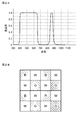
- FIG. 2A is a diagram illustrating an example of spectral characteristics of a dual band-pass filter disposed in front of an imaging device
- FIG. 2B is a diagram illustrating an R, G, B, and W color filter array.
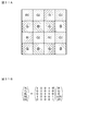
- FIG. 3A is a diagram illustrating a unit pixel array of a color filter according to the first embodiment
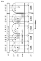
- FIG. 3B is a diagram illustrating an example of spectral characteristics of a selective infrared light blocking filter.
- FIG. 4 is a cross-sectional view illustrating a configuration of a color filter of each pixel of the pixel array unit.
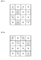
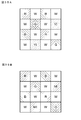
- FIG. 5A is a diagram illustrating a color filter array according to a first modification of the first embodiment
- FIG. 5B is a diagram illustrating a color filter array according to a second modification of the first embodiment
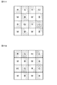
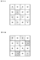
- FIG. 6A is a diagram illustrating a color filter array according to a third modification of the first embodiment
- FIG. 6B is a diagram illustrating a color filter array according to a fourth modification of the first embodiment
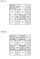
- FIG. 7A is a diagram illustrating a color filter array according to a fifth modification of the first embodiment
- FIG. 7B is a diagram illustrating a color filter array according to a fifth modification of the first embodiment
- FIG. 8A is a diagram illustrating a color filter array according to the second embodiment
- FIG. 8B is a diagram illustrating a color filter array according to a modification of the second embodiment.
- FIG. 9 is a diagram illustrating a unit pixel array of a color filter according to the third embodiment.
- FIG. 10A is a diagram illustrating a color filter array according to a first modification of the third embodiment
- FIG. 10B is a diagram illustrating a color filter array according to a second modification of the third embodiment.
- FIG. 11 is a diagram illustrating a color filter array according to the fourth embodiment.
- FIG. 12A is a diagram illustrating a color filter array according to a first modification of the fourth embodiment
- FIG. 12B is a diagram illustrating a color filter array according to a second modification of the fourth embodiment.
- FIG. 12A is a diagram illustrating a color filter array according to a first modification of the fourth embodiment
- FIG. 12B is a diagram illustrating a color filter array according to a second modification of the fourth embodiment.
- FIG. 13A is a diagram illustrating a color filter array according to the fifth embodiment
- FIG. 13B is a diagram illustrating a color filter array according to a modification of the fifth embodiment
- FIG. 14A is a diagram illustrating a color filter array according to the sixth embodiment
- FIG. 14B is a diagram illustrating a color filter array according to a modification of the sixth embodiment
- FIG. 15 is a diagram illustrating a color filter array according to the seventh embodiment.
- FIG. 16A is a diagram illustrating a color filter array according to a first modification of the seventh embodiment
- FIG. 16B is a diagram illustrating a color filter array according to a second modification of the seventh embodiment.
- FIG. 17 is a diagram illustrating a color filter array according to the eighth embodiment.
- FIG. 16A is a diagram illustrating a color filter array according to a first modification of the seventh embodiment
- FIG. 16B is a diagram illustrating a color filter array according to a second modification of the seventh embodiment
- FIG. 17 is
- FIG. 18A is a diagram illustrating a color filter array according to a first modification of the eighth embodiment
- FIG. 18B is a diagram illustrating a color filter array according to a second modification of the eighth embodiment
- FIG. 19A is a diagram illustrating a color filter array according to the ninth embodiment.
- FIG. 19B is a diagram illustrating a color filter array according to a first modification of the ninth embodiment.
- FIG. 20A is a diagram illustrating a color filter array according to a second modification of the ninth embodiment, and FIG. 20B is a diagram illustrating a color filter array according to a third modification of the ninth embodiment.
- FIG. 21A is a diagram illustrating a color filter array according to the tenth embodiment
- FIG. 21B is a diagram illustrating a color filter array according to a first modification of the tenth embodiment.
- FIG. 22A is a diagram illustrating a color filter array according to a second modification of the tenth embodiment
- FIG. 22B is a diagram illustrating a color filter array according to a third modification of the tenth embodiment.
- FIG. 23A is a diagram illustrating a color filter array according to a fourth modification of the tenth embodiment
- FIG. 23B is a diagram illustrating a color filter array according to a fifth modification of the tenth embodiment.
- FIG. 24A is a diagram illustrating a color filter array according to the eleventh embodiment
- FIG. 24B is a diagram illustrating a color filter array according to a first modification of the eleventh embodiment.
- FIG. 25A is a diagram illustrating a color filter array according to a second modification of the eleventh embodiment
- FIG. 25B is a diagram illustrating a color filter array according to a third modification of the eleventh embodiment.
- FIG. 26A is a diagram illustrating a color filter array according to a fourth modification of the eleventh embodiment
- FIG. 26B is a diagram illustrating a color filter array according to a fifth modification of the eleventh embodiment.
- FIG. 27A is a diagram illustrating a color filter array according to the twelfth embodiment
- FIG. 27B is a diagram illustrating a color filter array according to a first modification of the twelfth embodiment.
- FIG. 28A is a diagram illustrating a color filter array according to a second modification of the twelfth embodiment.
- FIG. 28B is a diagram illustrating a color filter array according to a third modification of the twelfth embodiment.
- FIG. 29A is a diagram illustrating a color filter array according to a fourth modification of the twelfth embodiment.
- FIG. 29B is a diagram illustrating a color filter array according to a fifth modification of the twelfth embodiment.
- FIG. 30 is a diagram illustrating a color filter array according to the thirteenth embodiment.
- FIG. 31A is a diagram illustrating a color filter array in which each pixel signal including the transmittance k cannot be obtained, and FIG.
- FIG. 31B is a diagram illustrating a conversion formula in the case of the color filter array.
- FIG. 32A is a diagram illustrating a color filter array according to variation 1
- FIG. 32B is a diagram illustrating a color filter array according to variation 2.
- FIG. 33A is a diagram illustrating a color filter array according to variation 3
- FIG. 33B is a diagram illustrating a color filter array according to variation 4.
- FIG. 34A is a diagram illustrating a color filter array according to variation 5
- FIG. 34B is a diagram illustrating a color filter array according to variation 6.
- FIG. 35A is a diagram illustrating a color filter array according to variation 7, and FIG. 35B is a diagram illustrating a color filter array according to variation 8.
- FIG. 32A is a diagram illustrating a color filter array according to variation 1
- FIG. 32B is a diagram illustrating a color filter array according to variation 2.
- FIG. 33A is a diagram illustrating a color filter array according to variation 3
- FIG. 36A is a diagram illustrating a color filter array according to Variation 9
- FIG. 36B is a diagram illustrating a color filter array according to Variation 10.
- FIG. 37A is a diagram illustrating a color filter array according to Variation 11
- FIG. 37B is a diagram illustrating a color filter array according to Variation 12.
- FIG. 38A is a diagram illustrating a color filter array according to Variation 13
- FIG. 38B is a diagram illustrating a color filter array according to Variation 14.
- FIG. 39A is a diagram illustrating a color filter array according to Variation 15, and
- FIG. 39B is a diagram illustrating a color filter array according to Variation 16.
- FIG. 40 is a diagram showing a color filter array according to variation 17.
- Embodiment 2 (Example in which half of W pixels are replaced with GI pixels based on the pixel array of R, G, B, and W) 3-3.
- Embodiment 3 (example based on R, G, B-IR pixel array) 3-4.
- Embodiment 4 (Example in which the number of G pixels is increased based on the pixel array of R, G, B-IR) 3-5.
- Embodiment 5 Example in which half of the G pixels are replaced with WS pixels based on the R, G, B-IR pixel array) 3-6.
- Embodiment 6 (Example in which half of IR pixels are replaced with kIR pixels based on a pixel array of R, G, B-IR) 3-7.
- Embodiment 7 (Example in which half of IR pixels are replaced with W pixels in the R, G, B-IR pixel array) 3-8.
- Embodiment 8 (Example in which half of G pixels are replaced with IR pixels in the pixel array of R, G, B, and W) 3-9.
- Embodiment 9 (Example based on R, B, W, WS-IR pixel array) 3-10.
- Embodiment 10 Example in which half of R pixels are replaced with YI pixels based on the pixel array of R, G, B-IR
- Embodiment 11 (Example in which half of R pixels are replaced with Ye pixels based on the pixel array of R, G, B-IR) 3-12.
- Embodiment 12 (example in which all color filters are replaced with complementary color filters) 3-13.
- Embodiment 13 (Example in which unit pixel arrays for calculating transmittance are discretely arranged) 4. Modified example of embodiment5. Configurations that the present disclosure can take
- a wavelength band corresponding to red a wavelength band corresponding to green, a wavelength band corresponding to blue, and a band having a longer wavelength than the wavelength band corresponding to red.
- the configuration may further include a bandpass filter that transmits the first infrared light wavelength band.
- the bandpass filter includes a first wavelength band that is a wavelength band between a wavelength band corresponding to red and a first infrared light wavelength band, and a wavelength band longer than the first infrared light wavelength band. Has a function of blocking the second wavelength band.
- the bandpass filter it is preferable to use a selective infrared light cutoff filter that restricts transmission in the first infrared light wavelength band.
- the first color filter is a red color filter
- the second color filter is a green color filter
- the third color filter is blue.
- the present invention can be configured.
- the fourth pixel has a white pixel on which no color filter is formed, or a transmission characteristic that transmits an infrared light wavelength band. It can be configured to be an infrared light pixel having
- the fifth pixel is a green pixel having no selective infrared light blocking filter, a white pixel having a selective infrared light blocking filter, and an infrared pixel having a selective infrared light blocking filter.
- An optical pixel or a complementary color pixel in which a selective infrared light blocking filter is not formed can be employed.
- the first color filter, the second color filter, and the third color filter are configured to be complementary color filters. be able to.
- the first color filter may be a yellow color filter
- the second color filter may be a magenta color filter
- the third color filter may be a cyan color filter.
- the fourth pixel is configured to be an infrared pixel having a transmission characteristic of transmitting a wavelength band of infrared light.
- the fifth pixel may be configured to be a yellow color filter, a magenta color filter, or a cyan color filter in which the selective infrared light blocking filter is not formed.
- the unit including the first pixel, the second pixel, the third pixel, the fourth pixel, and the fifth pixel
- the pixel array may be configured to be discretely arranged on a pixel array section in which pixels are arranged in a matrix.
- FIG. 1 shows a schematic configuration of a camera system using the imaging device of the present disclosure.
- a camera system 1 according to the present example has a configuration including a light source unit 10 that emits infrared light (IR), an imaging unit 20 that captures an image, and a camera signal processing unit 30. ing.
- the light source unit 10 includes an IR-LED 11 that is a light source that emits infrared light (IR), and an IR-LED driver 12 that drives the IR-LED 11.
- IR-LED 11 for example, a light emitting diode (LED) that emits infrared light having a wavelength of 850 nm is used.
- the imaging unit 20 includes a lens 21, a dual bandpass filter 22, and an imaging device 23. Then, as the imaging device 23, an imaging device of the present disclosure described later is used.
- an imaging device of the present disclosure for example, a CMOS (Complementary Metal Oxide Semiconductor) image sensor, which is a kind of an XY address type imaging device, can be exemplified.
- a CMOS image sensor is an image sensor manufactured by applying or partially using a CMOS process.
- the dual band pass filter 22 has a wavelength band corresponding to red (R), a wavelength band corresponding to green (G), a wavelength band corresponding to blue (B), and a wavelength longer than the wavelength band corresponding to red.
- This is a bandpass filter that transmits a first infrared light wavelength band that is a band.
- the dual bandpass filter 22 has a second wavelength band that is a wavelength band between the wavelength band corresponding to red and the first infrared light wavelength band, and a wavelength band longer than the infrared light wavelength band. It has a function of blocking the third wavelength band.
- FIG. 2A shows an example of the spectral characteristics of the dual bandpass filter 22. As shown in FIG. 2A, the dual bandpass filter 22 exemplified here has transmission characteristics in a visible light band and a first infrared light wavelength band corresponding to infrared light having a wavelength of 850 nm.
- the imaging device 23 is an imaging device capable of simultaneously acquiring visible light and infrared light.
- a color filter having a pixel array of R, G, B, and IR is used in order to prevent infrared light from entering a pixel for receiving visible light.
- color filters of the R, G, B, and IR pixel arrays are used as color filters to enable simultaneous acquisition of visible light and infrared light. Filters are known.
- W means a white pixel on which no color filter is formed.
- the W pixel is a pixel having sensitivity in all bands of visible light and infrared light corresponding to the sensitivity of the silicon substrate itself on which the pixel array is formed by not providing a color filter on the pixel.
- FIG. 2B shows an R, G, B, W color filter array according to a conventional example.
- the light receiving signal of each pixel is expressed by the following equation (1).
- the signal intensity of each color is calculated.
- the transmittance of the selective infrared light blocking filter exhibits instability over time and spatially, and thus it is assumed that the transmittance is close to 33%. Therefore, on the premise of such a change, it becomes difficult to use a selective infrared light blocking filter having a finite transmittance in the R, G, B, W color filter array (pixel array).
- the infrared light transmittance k of the selective infrared light blocking filter is unknown, or is spatially and temporally unstable, more accurate.
- a selective infrared light cutoff filter can be used, and similarly, visible light and infrared light can be separated more accurately. I do.
- the presence or absence of a selective infrared light blocking filter is included in the unit pixel array of the color filter of the imaging device according to the present disclosure. , A new pixel configuration is increased, and an input signal is calculated for each unit pixel array including the transmittance of the selective infrared light cutoff filter.
- the imaging device includes a first pixel, a second pixel, a third pixel, a fourth pixel, and a second pixel having the following functions in a unit pixel array of a color filter. , And a fifth pixel.
- the first pixel has a first color filter that transmits a wavelength band corresponding to the first color light that is visible light, and an infrared light cutoff filter that restricts transmission of an infrared light wavelength band.
- the second pixel has a second color filter that transmits a wavelength band corresponding to the second color light that is visible light, and an infrared light cutoff filter.
- the third pixel has a third color filter that transmits a wavelength band corresponding to the third color light that is visible light, and an infrared light cutoff filter.
- the fourth pixel has a transmission characteristic of transmitting a wavelength band of infrared light.
- the fifth pixel has a wavelength transmission characteristic different from any of the first pixel, the second pixel, the third pixel, and the fourth pixel.
- the first embodiment is an example based on a pixel array of R, G, B, and W.
- FIG. 3A shows a unit pixel array of the color filter according to the first embodiment.
- each filter is repeatedly developed on each pixel of the pixel array unit in units of a color filter array (pixel array) of 4 rows ⁇ 4 columns shown in FIG. 3A.
- a selective infrared light blocking filter is formed on two G pixels, and the other two G pixels are formed on the other two G pixels.
- the selective infrared light blocking filter is a filter having an absorption characteristic in a wavelength region substantially the same as the wavelength band of the projected infrared light.
- FIG. 4 shows a configuration of a filter of each pixel in a pixel array section in which pixels are arranged in a matrix.
- FIG. 4 is a cross-sectional view of a B pixel, a G pixel, an R pixel, and a GI pixel, and a cross-sectional view of a W pixel, taken along line XX of FIG. 3A.
- the GI pixel is a G pixel on which the selective infrared light blocking filter is not formed.
- a G pixel on which the selective infrared light blocking filter is not formed is referred to as a GI pixel.
- the GI pixel is a pixel having sensitivity to two wavelength bands, that is, a G wavelength band and a wavelength band of infrared light transmitted through the dual bandpass filter 22.
- FIG. 3B shows an example of the spectral characteristics of the selective infrared light blocking filter.
- the transmittance of infrared light near 850 nm is about 12%, but this transmittance tends to vary in the plane of the imaging device 23 or to vary over time. is there.
- an infrared light blocking filter that blocks infrared light (IR), for example, a wavelength band substantially equal to the wavelength band of infrared light emitted from a light source.
- a selective infrared light cutoff filter 232 having absorption characteristics in the same wavelength region, that is, the first infrared wavelength band, and restricting transmission in the first wavelength band is formed.
- a color filter 233 corresponding to each pixel is formed on the selective infrared light blocking filter 232.
- the selective infrared light cutoff filter 232 for limiting the transmission of the first infrared light wavelength band is not formed, and only the G color filter is formed.
- No color filter is formed for the W pixel, and the W pixel has sensitivity in all bands of visible light and infrared light corresponding to the sensitivity of the silicon substrate itself.
- an on-chip lens 234 is formed for each pixel.
- each of the R, G, and B pixels includes the first color light (red light), the second color light (green light), and the third color light (blue), which are visible lights. 1, 2, and 3, which have filters that transmit a wavelength band corresponding to light, and a selective infrared light cutoff filter 232.
- the W pixel is a fourth pixel having a transmission characteristic of transmitting a wavelength band of infrared light.
- the GI pixel is a fifth pixel having a wavelength transmission characteristic different from any of the first pixel, the second pixel, the third pixel, and the fourth pixel.
- the optical signal incident on each pixel forming the unit pixel array corresponds to the R, G, B, IR, and kIR of the color filter according to the layered configuration of the color filters. It is classified into five types.
- kIR means infrared light transmitted through the selective infrared light cutoff filter 232, and its intensity is obtained by multiplying the infrared light intensity IR by the infrared light transmittance k.
- 1 and 0 are simply arranged, but in detail, they can be described as real-valued components based on the spectral characteristics of each filter. It is possible. The same applies to each embodiment described later.
- the difference from the above-described R, G, B, W color filter array according to the conventional example is that the number of GI pixels is increased as the types of pixels, and correspondingly, the intensity of kIR is also unknown.
- the conversion matrix A between the incident signal intensity and the pixel signal has 5 rows ⁇ 5 columns by using the coefficients. From this, if there is an inverse matrix of the transformation matrix A (determinant detA ⁇ 0), the inverse matrix operation is performed to obtain the R, G, B, IR, and kIR signals separated from the five types of incident signal values. The value can be calculated.
- the following equation (4) shows an arithmetic expression for actually obtaining the inverse matrix of the conversion matrix A and separating the R, G, B, kIR, and IR incident signal intensities from the pixel signal.
- each signal strength can be calculated.
- the infrared light transmittance k of the selective infrared light cutoff filter 232 can be obtained for each unit pixel array.
- the infrared light transmittance k of the selective infrared light blocking filter or the infrared light component kIR multiplied by the infrared light transmittance k can be obtained for each unit pixel array. Therefore, it is affected by the spatial and temporal fluctuation of the infrared light transmittance k of the selective infrared light blocking filter, which is a problem in the R, G, B, W color filter arrangement according to the conventional example described above. Without this, it is possible to separate and calculate the visible light component and the infrared light component with higher accuracy. Further, it is possible to avoid the problem of divergence of the solution, which is a problem in the R, G, B, W color filter arrangement according to the conventional example.
- An effect similar to that of the color filter array according to the first embodiment is that a selective infrared light blocking filter is used for pixels of each color (including IR (infrared light) and all-light (W) transmissive pixels) constituting the unit pixel array. If the conversion matrix corresponding to the equation (3) has an inverse matrix (determinant det ⁇ 0), the pixel can be obtained in another arrangement.
- 5A and 5B show modified examples of the color filter array of 4 rows ⁇ 4 columns repeated
- FIGS. 6A, 6B, 7A, and 7B show modified examples of the color filter array of 2 rows ⁇ 2 columns repeated. Show.
- FIG. 5A shows a color filter array according to a first modification of the first embodiment.
- the GI pixel is replaced with the G pixel in the color filter array according to the first embodiment (see FIG. 3A), and the R pixel in the third row and the third column is selectively blocked with infrared light.
- the configuration is such that the pixel is replaced with an RI pixel on which no filter is formed.
- the RI pixel is an R pixel having sensitivity in two wavelength bands of an R wavelength band and a wavelength band of infrared light transmitted through the dual bandpass filter 22.
- FIG. 5B shows a color filter array according to a second modification of the first embodiment.
- the GI pixel is replaced with the G pixel in the color filter array according to the first embodiment (see FIG. 3A), and the B pixel in the third row and the first column is selectively blocked with infrared light.
- the configuration is such that the pixel is replaced with a BI pixel on which no filter is formed.
- the BI pixel is a B pixel having sensitivity to two wavelength bands, a B wavelength band and a wavelength band of infrared light transmitted through the dual bandpass filter 22.
- FIG. 6A shows a color filter array according to a third modification of the first embodiment.
- pixel units of 2 rows ⁇ 2 columns of R, W, G, B and pixel units of 2 rows ⁇ 2 columns of R, W, GI, B are alternately arranged.
- the GI pixel is a pixel having sensitivity to two wavelength bands, that is, a G wavelength band and a wavelength band of infrared light transmitted through the dual bandpass filter 22.
- FIG. 6B shows a color filter array according to a fourth modification of the first embodiment.
- pixel units of 2 rows ⁇ 2 columns of R, W, G, B and pixel units of 2 rows ⁇ 2 columns of RI, W, G, B are alternately arranged.
- the RI pixel is an R pixel having sensitivity in two wavelength bands of an R wavelength band and a wavelength band of infrared light transmitted through the dual bandpass filter 22.
- FIG. 7A shows a color filter array according to a fifth modification of the first embodiment.
- pixel units of 2 rows ⁇ 2 columns of R, W, G, B and pixel units of 2 rows ⁇ 2 columns of R, W, G, BI are alternately arranged.
- the BI pixel is a B pixel having sensitivity to two wavelength bands, a B wavelength band and a wavelength band of infrared light transmitted through the dual bandpass filter 22.
- FIG. 7B shows a color filter array according to a sixth modification of the first embodiment.
- pixel units of 2 rows ⁇ 2 columns of R, W, G, B and pixel units of 2 rows ⁇ 2 columns of R, WS, G, B are alternately arranged.
- the WS pixel is a W pixel on which a selective infrared light blocking filter is formed.
- Example 2 in the color filter array based on the R, G, B, and W pixel arrays, half of the W pixels are assigned to the G wavelength band and the wavelength of the infrared light transmitted through the dual bandpass filter 22. This is an example in which GI pixels having sensitivity to two wavelength bands are replaced.
- FIG. 8A shows a color filter array according to the second embodiment.
- the first row in the pixel array of 4 rows ⁇ 4 columns, the first row includes an R pixel, a GI pixel, a B pixel, and a GI pixel.
- the fourth row has W pixels, G pixels, W pixels, and G pixels, and the third row has G pixels, GI pixels, R pixels, and GI pixels.
- the R pixel, the G pixel, and the B pixel are pixels on which a selective infrared light blocking filter is formed
- the GI pixel and the W pixel are pixels on which a selective infrared light blocking filter is not formed. is there.
- the conversion matrix operation formula of the color filter array according to the second embodiment is the same as that of the first embodiment.
- the color filter array according to the second embodiment the color filter configuration of the R, G, B pixels is the same as the R, G, B, W color filter array according to the conventional example (see FIG. 2B). Therefore, even when the intensity of the infrared light is high, the quality of the color image can be maintained as it is.
- the visible light can be reflected with higher accuracy without being affected by the spatial and temporal fluctuations of the transmittance k of the selective infrared light cutoff filter.
- the infrared light component can be separately calculated, and the quality of the color image can be maintained as it is even when the intensity of the infrared light is high.
- FIG. 8B shows a color filter array according to a modification of the second embodiment.
- the color filter array according to the modification of the second embodiment in a color filter array of 4 rows ⁇ 4 columns repeated based on the pixel array of R, G, B, and W, half of the W pixels are selectively used as W pixels. This is an example in which the pixel is replaced with a WS pixel on which an infrared light cutoff filter 232 is formed.
- the inverse matrix of the transformation matrix is obtained, and the inverse transformation is performed to separate and calculate each signal component of R, G, B, kIR, and IR from the signal intensity of each pixel. It becomes possible to do.
- the sensitivity to visible light (R, B) components is reduced.
- half of the W pixels are replaced with WS pixels, so that the sensitivity to the visible light (R, G, B) components can be maintained. It becomes possible.
- the third embodiment is an example of a color filter array of 2 rows ⁇ 2 columns repeated based on a pixel array of R, G, B-IR (infrared light).
- FIG. 9 shows a color filter array according to the third embodiment.
- the difference between the color filter array according to the third embodiment and the color filter array according to the first embodiment is that there is no W pixel, as is apparent from FIG. That is, in the third embodiment, the pixel arrangement is such that the W pixels are replaced with the IR pixels, and each filter is repeatedly developed on each pixel of the pixel array unit with the pixel array of 4 rows ⁇ 4 columns as a unit. .
- the IR pixel is a pixel having a transmission characteristic of transmitting a wavelength band of infrared light.
- a selective infrared light blocking filter is formed on each of the R, G, and B pixels, and two G pixels out of the four G pixels existing in the color filter array.
- a pixel is provided with a selective infrared light blocking filter, and the other two G pixels (that is, GI pixels) are not provided with a selective infrared light blocking filter.
- the first row includes an R pixel, a GI pixel, an R pixel, and a G pixel.
- the fourth row has IR pixels, B pixels, IR pixels, and B pixels
- the third row has R pixels, G pixels, R pixels, and GI pixels.
- the R pixel, the G pixel, the B pixel, and the IR pixel are pixels on which a selective infrared light blocking filter is formed
- the GI pixel is a pixel on which no selective infrared light blocking filter is formed. is there.
- each of the R, G, and B pixels includes the first color light (red light), the second color light (green light), and the third color light (blue), which are visible lights.
- first, second, and third pixels each having a filter that transmits a wavelength band corresponding to light, and a selective infrared light cutoff filter.
- the IR pixel is a fourth pixel having a transmission characteristic of transmitting a wavelength band of infrared light.
- the GI pixel is a fifth pixel having a wavelength transmission characteristic different from any of the first pixel, the second pixel, the third pixel, and the fourth pixel.
- the relationship between the intensity of each color component and the signal intensity of each pixel is as follows. It is represented by a matrix operation as shown in equation (7). As in the case of the first embodiment, a conversion equation of 5 rows ⁇ 5 columns is obtained by setting the kIR obtained by multiplying the infrared light transmittance k of the selective infrared light cutoff filter by the infrared light intensity to be an unknown number. .
- the inverse matrix of the conversion matrix is obtained, and the inverse transformation is performed to obtain the signal intensity of each pixel, including the infrared light transmittance k of the selective infrared light cutoff filter. , R, G, B, kIR, and IR signal components.
- the same operation and effect as those in the first embodiment based on the R, G, B, W pixel array can be obtained.
- FIG. 10A shows a color filter array according to a first modification of the third embodiment.
- the color filter array according to the first modification is different from the color filter array according to the third embodiment (see FIG. 9) in that each R pixel in the third row and the first column and the first row and the third column is selectively infrared-blocked.
- RI pixels having sensitivity in two wavelength bands of the R wavelength band and the infrared light wavelength band transmitted through the dual band-pass filter 22. .
- FIG. 10B shows a color filter array according to a second modification of the third embodiment.
- each B pixel in the fourth row and the second column and the second row and the fourth column is set to a selective infrared light blocking filter.
- Ie a BI pixel having sensitivity in two wavelength bands of the B wavelength band and the infrared light wavelength band transmitted through the dual bandpass filter 22. .
- Example 4 in the color filter array of 4 rows ⁇ 4 columns repeated based on the pixel array of R, G, B-IR, the number of G pixels having a high effect on the resolution is increased, and the R pixels having a low effect on the resolution are increased. And the number of B pixels is reduced.
- FIG. 11 shows a color filter array according to the fourth embodiment.
- the fourth embodiment in the pixel array of R, G, and B-IR, out of a total of 16 pixels of 4 rows ⁇ 4 columns, half of the G pixels are G pixels, and the eight Of the G pixels, four G pixels are provided with a selective infrared light blocking filter, and the other four G pixels are not provided with a selective infrared light blocking filter. Then, the signal value of each filter can be calculated by the same conversion equation in the case of the third embodiment.
- the first row is composed of R pixels, G pixels, B pixels, and G pixels
- the second and fourth rows are composed of GI pixels, IR pixels, and GI pixels
- the third row is composed of B pixels, G pixels, R pixels, and G pixels.
- the R pixel, the G pixel, the B pixel, and the IR pixel are pixels on which a selective infrared light blocking filter is formed
- the GI pixel is a pixel on which no selective infrared light blocking filter is formed. is there.
- the fourth embodiment since the pixel array of R, G, and B-IR is basically used, the same operation and effect as those of the third embodiment can be obtained.
- the number of G pixels having a high effect on resolution is larger than the number of R pixels and B pixels, so that higher resolution can be achieved.
- FIG. 12A shows a color filter array according to a first modification of the fourth embodiment.
- the GI pixel is replaced with the G pixel in the color filter array according to the fourth embodiment (see FIG. 11), and the R pixel in the third row and the third column is selectively infrared light.
- the configuration is such that the pixel is replaced with an RI pixel having no cutoff filter.
- FIG. 12B shows a color filter array according to a second modification of the fourth embodiment.
- the GI pixel is replaced with the G pixel in the color filter array according to the fourth embodiment (see FIG. 11), and the B pixel in the third row and the first column is selectively infrared light.
- the GI pixel is not provided with a cutoff filter.
- Example 5 in a color filter array having a repetition of 4 rows ⁇ 4 columns based on a pixel array of R, G, and B-IR, half of the G pixels are replaced with WS pixels on which a selective infrared light blocking filter is formed. This is an example of replacing with.
- FIG. 13A shows a color filter array according to the fifth embodiment.
- the color filter array according to the fifth embodiment in the R, G, and B-IR pixel arrays, half of the G pixels are replaced with WS pixels, and G pixels, WS pixels, and IR pixels are used.
- WS pixels are arranged four by four.
- the first row is composed of R pixels, G pixels, B pixels, and G pixels
- the second and fourth rows are WS pixels, IR pixels, and WS pixels.
- the third row is composed of B pixels, G pixels, R pixels, and G pixels.
- the WS pixel is a W pixel on which a selective infrared light blocking filter is formed.
- each of the R, G, and B pixels includes the first color light (red light), the second color light (green light), and the third color light (blue), which are visible lights. 1), first, second, and third pixels each having a filter that transmits a wavelength band corresponding to light, and a selective infrared light cutoff filter.
- the IR pixel is a fourth pixel having a transmission characteristic of transmitting a wavelength band of infrared light.
- the WS pixel is a fifth pixel having a wavelength transmission characteristic different from any of the first pixel, the second pixel, the third pixel, and the fourth pixel.
- the relationship between the intensity of each color component and the signal intensity of each pixel is as follows. It is expressed by a matrix operation as shown in Expression (9).
- the inverse matrix of the conversion matrix is obtained, and the inverse transformation is performed to obtain the signal intensity of each pixel, including the infrared light transmittance k of the selective infrared light cutoff filter. , R, G, B, kIR, and IR signal components.
- FIG. 13B shows a color filter array according to a modification of the fifth embodiment.
- the color arrangement of the second and fourth rows is different from the pixel arrangement of the fifth embodiment (FIG. 13A).
- the second row and the fourth row are both WS pixels, IR pixels, WS pixels, and IR pixels.
- the second row has an array of WS pixels, B pixels, IR pixels, and B pixels
- the fourth row has IR pixels, B pixels, WS pixels, and B pixels. It is an array of.
- Example 6 in a color filter array based on the R, G, B-IR pixel array, half of the IR pixels are replaced with kIR pixels in which a selective infrared light cutoff filter is formed on the IR pixels. It is.
- FIG. 14A shows a color filter array according to the sixth embodiment.
- the first and third rows are composed of R pixels, G pixels, B pixels, and G pixels
- the second row is kIR pixels.
- the fourth row is composed of IR pixels, kIR pixels, R pixels, and B pixels.
- each of the R, G, and B pixels includes the first color light (red light), the second color light (green light), and the third color light (blue), which are visible lights.
- first, second, and third pixels each having a filter that transmits a wavelength band corresponding to light, and a selective infrared light cutoff filter.
- the IR pixel is a fourth pixel having a transmission characteristic of transmitting a wavelength band of infrared light.
- the kIR pixel is a fifth pixel having a wavelength transmission characteristic different from any of the first pixel, the second pixel, the third pixel, and the fourth pixel.
- the relationship between the intensity of each color component and the signal intensity of each pixel is as follows. It is represented by a matrix operation as shown in Expression (11).
- the inverse matrix of the conversion matrix is obtained, and the inverse transformation is performed to obtain the signal intensity of each pixel, including the infrared light transmittance k of the selective infrared light cutoff filter. , R, G, B, kIR, and IR signal components.
- the same operation and effect as those in the third embodiment can be obtained since the pixel array of R, G, and B-IR is used as a basis. Further, since half of the IR pixels are replaced with kIR pixels, the resolution of infrared light is degraded, but the infrared light transmittance k of the selective infrared light cutoff filter can be calculated with the IR pixels and the kIR pixels. Will be possible.
- FIG. 14B shows a color filter array according to a modification of the sixth embodiment.
- the first row includes R pixels, G pixels, B pixels, and G pixels
- the second row includes G pixels, kIR pixels
- the third row is composed of B pixels, G pixels, IR pixels, and G pixels
- the fourth row is composed of G pixels, IR pixels, G pixels, and kIR pixels.
- Embodiment 7 is an example of a color filter array based on a pixel array of R, G, BW, and IR.
- FIG. 15 shows a color filter array according to the seventh embodiment.
- the color filter array according to the seventh embodiment has a configuration in which half of the IR pixels are replaced with W pixels in the pixel array of R, G, and B-IR according to the fourth embodiment (see FIG. 11).
- the color filter array according to the seventh embodiment includes a pixel unit of 2 rows ⁇ 2 columns of R, G, G, and IR and a pixel unit of 2 rows ⁇ 2 columns of B, G, G, W. Are arranged in a unit pixel array alternately arranged.
- the relationship between the intensity of each color component and the signal intensity of each pixel is as follows. It is represented by a matrix operation as shown in Expression (13).
- the inverse matrix of the conversion matrix is obtained, and the inverse transformation is performed to obtain the signal intensity of each pixel, including the infrared light transmittance k of the selective infrared light cutoff filter. , R, G, B, kIR, and IR signal components.
- the first embodiment based on the pixel array of R, G, B, and W, and the R, G, B-IR The same operation and effect as those in the third embodiment based on the pixel arrangement can be obtained. That is, since the infrared light transmittance k of the selective infrared light blocking filter or the infrared light component kIR multiplied by the infrared light transmittance k can be obtained for each unit pixel array, It is possible to separate and calculate the visible light component and the infrared light component with higher accuracy without being affected by the spatial and temporal fluctuation of the infrared light transmittance k of the light blocking filter.
- FIG. 16A shows a color filter array according to a first modification of the seventh embodiment.
- R, IR, G, B pixel units of 2 rows ⁇ 2 columns and R, W, G, B pixel units of 2 rows ⁇ 2 columns are alternately arranged.
- W, G, B pixel units of 2 rows ⁇ 2 columns are alternately arranged.
- FIG. 16B shows a color filter array according to a second modification of the seventh embodiment.
- pixel units of 2 rows ⁇ 2 columns of R, kIR, G, B and pixel units of 2 rows ⁇ 2 columns of R, W, G, B are alternately arranged.
- the unit pixel array is alternately arranged.
- Example 8 The eighth embodiment is also an example of a color filter array based on a pixel array of R, G, BW, and IR similarly to the seventh embodiment.
- FIG. 17 shows a color filter array according to the eighth embodiment.
- the color filter array according to the eighth embodiment has a configuration in which half of the G pixels are replaced with IR pixels in the pixel array of R, G, B, and W. More specifically, a unit pixel array in which pixel units of 2 rows ⁇ 2 columns of R, W, W, and IR and pixel units of 2 rows ⁇ 2 columns of B, W, W, and G are alternately arranged. It has a configuration.
- the conversion matrix operation formula of the color filter array according to the eighth embodiment is the same as that of the seventh embodiment.
- the first embodiment based on the pixel array of R, G, B, and W, and the R, G, B-IR The same operation and effect as those in the third embodiment based on the pixel arrangement can be obtained. That is, since the infrared light transmittance k of the selective infrared light blocking filter or the infrared light component kIR multiplied by the infrared light transmittance k can be obtained for each unit pixel array, It is possible to separate and calculate the visible light component and the infrared light component with higher accuracy without being affected by the spatial and temporal fluctuation of the infrared light transmittance k of the light blocking filter.
- FIG. 18A shows a color filter array according to a first modification of the eighth embodiment.
- the color filter array according to the first modification has a configuration in which the IR pixels are replaced with G pixels and half of the W pixels are replaced with IR pixels in the color filter array according to Embodiment 8 (see FIG. 17). More specifically, the color filter array according to the first modification includes a pixel unit of 2 rows ⁇ 2 columns of R, W, IR, and G and a pixel unit of 2 rows ⁇ 2 columns of B, W, IR, and G Are alternately arranged in a unit pixel array configuration.
- FIG. 18B shows a color filter array according to a second modification of the seventh embodiment.
- the color filter array according to the second modification has a configuration in which the IR pixels are replaced with G pixels and half of the W pixels are replaced with kIR pixels in the color filter array according to Embodiment 8 (see FIG. 17).
- the color filter array according to the second modification includes a pixel unit of 2 rows ⁇ 2 columns of R, W, kIR, G and a pixel unit of 2 rows ⁇ 2 columns of B, W, kIR, G. Are alternately arranged in a unit pixel array configuration.
- the ninth embodiment is an example of a color filter array based on a pixel array of R, B, W, and WS-IR.
- FIG. 19A shows a color filter array according to the ninth embodiment.
- the color filter array according to the ninth embodiment has a configuration in which the G pixel is replaced with a WS pixel and the GI pixel is replaced with a W pixel in the color filter array according to the fourth embodiment (see FIG. 11). More specifically, the color filter array according to the ninth embodiment includes a pixel unit of 2 rows ⁇ 2 columns of R, W, WS, and IR, and a pixel unit of 2 rows ⁇ 2 columns of B, W, WS, and IR. Are arranged in a unit pixel array alternately arranged. The G signal is calculated from other pixel signals.
- the relationship between the intensity of each color component and the signal intensity of each pixel is as follows. It is expressed by a matrix operation as shown in Expression (15).
- the inverse matrix of the conversion matrix is obtained, and the inverse transformation is performed to obtain the signal intensity of each pixel, including the infrared light transmittance k of the selective infrared light cutoff filter. , R, G, B, kIR, and IR signal components.
- the infrared light transmittance k of the selective infrared light cutoff filter or the infrared light transmittance k is multiplied.
- the infrared light component kIR can also be obtained for each unit pixel array. Therefore, it is possible to separate and calculate the visible light component and the infrared light component with higher accuracy without being affected by the spatial and temporal fluctuation of the infrared light transmittance k of the selective infrared light blocking filter.
- the sensitivity can be improved as compared with the case where the G pixel is not replaced.
- FIG. 19B shows a color filter array according to a first modification of the ninth embodiment.
- pixel units of 2 rows ⁇ 2 columns of R, W, WS, B and pixel units of 2 rows ⁇ 2 columns of R, IR, WS, B are alternately arranged.
- the unit pixel array is alternately arranged.
- FIG. 20A shows a color filter array according to a second modification of the ninth embodiment.
- the color filter array according to the second modification has a configuration in which IR pixels are replaced with kIR pixels in the color filter array according to the first modification (see FIG. 19B).
- the color filter array according to the second modification includes a pixel unit of 2 rows ⁇ 2 columns of R, W, WS, B, and a pixel unit of 2 rows ⁇ 2 columns of R, kIR, WS, B. Are alternately arranged in a unit pixel array configuration.
- FIG. 20B shows a color filter array according to a third modification of the ninth embodiment.
- the color filter array according to the third modification has a configuration in which half of the IR pixels are replaced with kIR pixels in the color filter array according to the ninth embodiment (see FIG. 19A).
- the color filter array according to the third modification includes a pixel unit of 2 rows ⁇ 2 columns of R, W, WS, and IR and a pixel unit of 2 rows ⁇ 2 columns of B, W, WS, and kIR. Are alternately arranged in a unit pixel array configuration.
- the tenth embodiment is an example of a color filter array in which R, G, and B color filters are replaced with complementary color filters.
- Examples of the complementary color filters include Ye (yellow), Mg (magenta), and Cy (cyan).
- FIG. 21A shows a color filter array according to the tenth embodiment.
- the color filter array according to the tenth embodiment has a configuration in which half of R pixels among R, G, and B are replaced with YI pixels in a color filter array based on an R, G, B-IR pixel array. ing.
- the color filter array according to the tenth embodiment has a pixel unit of 2 rows ⁇ 2 columns of R, IR, G, B, and a pixel unit of 2 rows ⁇ 2 columns of YI, IR, G, B. Are arranged in a unit pixel array alternately arranged.
- the YI pixel is a Ye pixel on which the selective infrared light blocking filter is not formed.
- each of the R, G, and B pixels includes the first color light (red light), the second color light (green light), and the third color light (blue), which are visible lights. 1, 2, and 3, which have filters that transmit a wavelength band corresponding to light, and a selective infrared light cutoff filter 232.
- the IR pixel is a fourth pixel having a transmission characteristic of transmitting a wavelength band of infrared light.
- the YI pixel which is a complementary color pixel is a fifth pixel having a wavelength transmission characteristic different from any of the first pixel, the second pixel, the third pixel, and the fourth pixel.
- the relationship between the intensity of each color component and the signal intensity of each pixel is as follows. It is expressed by a matrix operation as shown in Expression (17).
- the inverse matrix of the conversion matrix is obtained, and the inverse transformation is performed to obtain the signal intensity of each pixel, including the infrared light transmittance k of the selective infrared light cutoff filter. , R, G, B, kIR, and IR signal components.
- the infrared light transmittance k of the selective infrared light blocking filter or the infrared light can also be obtained for each unit pixel array. Therefore, it is possible to separate and calculate the visible light component and the infrared light component with higher accuracy without being affected by the spatial and temporal fluctuations of the infrared light transmittance k of the selective infrared light blocking filter. Becomes In addition, by adopting a configuration using complementary color filters, it becomes possible to increase the sensitivity of visible light as compared with the case where R, G, B color filters are used.
- FIG. 21B shows a color filter array according to a first modification of the tenth embodiment.
- the color filter array according to the first modification has a configuration in which the YI pixels are replaced with MI pixels in the color filter array according to the tenth embodiment (see FIG. 21A). More specifically, the color filter array according to the first modified example has a pixel unit of 2 rows ⁇ 2 columns of R, IR, G, B and a pixel unit of 2 rows ⁇ 2 columns of MI, IR, G, B. Are alternately arranged in a unit pixel array configuration.
- the MI pixel which is a complementary color pixel, is an Mg pixel on which a selective infrared light blocking filter is not formed, and includes a first pixel, a second pixel, a third pixel, and a fourth pixel. These are fifth pixels having different wavelength transmission characteristics.
- FIG. 22A shows a color filter array according to a second modification of the tenth embodiment.
- the color filter array according to the second modification has a configuration in which the YI pixels are replaced with the CI pixels in the color filter array according to the tenth embodiment (see FIG. 21A). More specifically, the color filter array according to the second modification includes a pixel unit of 2 rows ⁇ 2 columns of R, IR, G, B and a pixel unit of 2 rows ⁇ 2 columns of CI, IR, G, B. Are alternately arranged in a unit pixel array configuration.
- the CI pixel which is a complementary color pixel, is a Cy pixel on which the selective infrared light blocking filter is not formed, and includes a first pixel, a second pixel, a third pixel, and a fourth pixel. These are fifth pixels having different wavelength transmission characteristics.
- FIG. 22B shows a color filter array according to a third modification of the tenth embodiment.
- the color filter array according to the third modification has a configuration in which GI pixels are replaced with YI pixels in the color filter array according to the fourth embodiment (see FIG. 11).
- the color filter array according to the third modification includes a pixel unit of 2 rows ⁇ 2 columns of R, YI, G, and IR, and a pixel unit of 2 rows ⁇ 2 columns of B, YI, G, and IR. Are alternately arranged in a unit pixel array configuration.
- FIG. 23A shows a color filter array according to a fourth modification of the tenth embodiment.
- the color filter array according to the fourth modification has a configuration in which GI pixels are replaced with MI pixels in the color filter array according to the fourth embodiment (see FIG. 11). More specifically, the color filter array according to the fourth modification includes a pixel unit of 2 rows ⁇ 2 columns of R, MI, G, and IR, and a pixel unit of 2 rows ⁇ 2 columns of B, MI, G, and IR. Are alternately arranged in a unit pixel array configuration.
- FIG. 23B shows a color filter array according to a fifth modification of the tenth embodiment.
- the color filter array according to the fifth modification has a configuration in which GI pixels are replaced with CI pixels in the color filter array according to the fourth embodiment (see FIG. 11). More specifically, the color filter array according to the fifth modification includes a pixel unit of 2 rows ⁇ 2 columns of R, CI, G, and IR, and a pixel unit of 2 rows ⁇ 2 columns of B, CI, G, and IR. Are alternately arranged in a unit pixel array configuration.
- the eleventh embodiment is an example in which in a color filter array based on an R, G, B-IR pixel array, half of the R pixels of R, G, B are replaced with Ye pixels.
- the Ye pixel is a pixel on which a selective infrared light blocking filter is formed.
- FIG. 24A shows a color filter arrangement according to the eleventh embodiment.
- the color filter array according to the eleventh embodiment has a configuration in which the YI pixel is replaced with the Ye pixel in the color filter array according to the tenth embodiment (see FIG. 21A).
- the color filter array according to the eleventh embodiment has a pixel unit of 2 rows ⁇ 2 columns of R, IR, G, B, and a pixel unit of 2 rows ⁇ 2 columns of Ye, IR, G, B. Are arranged in a unit pixel array alternately arranged.
- the Ye pixel is a pixel on which a selective infrared light blocking filter is formed.
- the relationship between the intensity of each color component and the signal intensity of each pixel is as follows. It is represented by a matrix operation as shown in Expression (19).
- the inverse matrix of the conversion matrix is obtained, and the inverse transformation is performed to obtain the signal intensity of each pixel and the infrared light transmittance k of the selective infrared light cutoff filter. , R, G, B, kIR, and IR signal components.
- the infrared light transmittance of the selective infrared light blocking filter is also k or an infrared light component kIR multiplied by the infrared light transmittance k can also be obtained for each unit pixel array. Therefore, it is possible to separate and calculate the visible light component and the infrared light component with higher accuracy without being affected by the spatial and temporal fluctuation of the infrared light transmittance k of the selective infrared light blocking filter. Becomes Also, as in the case of the tenth embodiment, by employing a configuration using a complementary color filter, it becomes possible to increase the sensitivity of visible light as compared with the case of using R, G, B color filters.
- FIG. 24B shows a color filter array according to a first modification of the eleventh embodiment.
- the color filter array according to the first modification has a configuration in which the Ye pixel is replaced with the M pixel in the color filter array according to the eleventh embodiment (see FIG. 24A). More specifically, the color filter array according to the first modified example has a pixel unit of 2 rows ⁇ 2 columns of R, IR, G, B and a pixel unit of 2 rows ⁇ 2 columns of Mg, IR, G, B. Are alternately arranged in a unit pixel array configuration.
- the Mg pixel is a pixel on which a selective infrared light blocking filter is formed.
- FIG. 25A shows a color filter array according to a second modification of the eleventh embodiment.
- the color filter array according to the second modification has a configuration in which the Ye pixel is replaced with the Cy pixel in the color filter array according to the eleventh embodiment (see FIG. 24A).
- the color filter arrangement g column according to the second modified example includes a pixel unit of 2 rows ⁇ 2 columns of R, IR, G, B and a 2 rows ⁇ 2 column of Cy, IR, G, B. It has a configuration of a unit pixel array in which pixel units are alternately arranged.
- the Cy pixel is a pixel on which a selective infrared light blocking filter is formed.
- FIG. 25B shows a color filter array according to a third modification of the eleventh embodiment.
- the color filter array according to the third modification has a configuration in which GI pixels are replaced with Ye pixels in the color filter array according to the fourth embodiment (see FIG. 11).
- the color filter array according to the third modification includes a pixel unit of 2 rows ⁇ 2 columns of R, Ye, G, and IR, and a pixel unit of 2 rows ⁇ 2 columns of B, Ye, G, and IR. Are alternately arranged in a unit pixel array configuration.
- FIG. 26A shows a color filter array according to a fourth modification of the eleventh embodiment.
- the color filter array according to the fourth modification has a configuration in which GI pixels are replaced with Mg pixels in the color filter array according to the fourth embodiment (see FIG. 11). More specifically, the color filter array according to the fourth modification includes a pixel unit of 2 rows ⁇ 2 columns of R, Mg, G, and IR, and a pixel unit of 2 rows ⁇ 2 columns of B, Mg, G, and IR. Are alternately arranged in a unit pixel array configuration.
- FIG. 26B shows a color filter array according to a fifth modification of the tenth embodiment.
- the color filter array according to the fifth modification has a configuration in which GI pixels are replaced with Cy pixels in the color filter array according to the fourth embodiment (see FIG. 11). More specifically, the color filter array according to the fifth modification includes a pixel unit of 2 rows ⁇ 2 columns of R, Cy, G, and IR and a pixel unit of 2 rows ⁇ 2 columns of B, Cy, G, and IR. Are alternately arranged in a unit pixel array configuration.
- Embodiment 12 is an example in which all color filters are replaced with complementary color filters.
- complementary color filters Ye (yellow), Mg (magenta), and Cy (cyan) can be exemplified as in the case of the tenth and eleventh embodiments.
- FIG. 27A shows a color filter array according to the twelfth embodiment.
- the color filter array according to the twelfth embodiment has a configuration in which the R pixel is replaced with a Ye pixel, the G pixel is replaced with a Mg pixel, and the B pixel is replaced with a Cy pixel in the color filter array according to the tenth embodiment (see FIG. 21A).
- the color filter array according to the twelfth embodiment includes a pixel unit of 2 rows ⁇ 2 columns of Ye, IR, Mg, and Cy, and a pixel unit of 2 rows ⁇ 2 columns of YI, IR, Mg, and Cy. Are arranged in a unit pixel array alternately arranged.
- the Ye pixel, the Mg pixel, and the Cy pixel are pixels on which a selective infrared light blocking filter is formed, and the YI pixel is a Ye pixel on which a selective infrared light blocking filter is not formed. is there.
- each of the pixels of Ye, Mg, and Cy has the first color light (yellow color light), the second color light (magenta color light), and the third color light (cyan), which are visible lights.
- the first, second, and third pixels each have a filter that transmits a wavelength band corresponding to (color light) and a selective infrared light cutoff filter 232.
- the IR pixel is a fourth pixel having a transmission characteristic of transmitting a wavelength band of infrared light.
- the YI pixel is a fifth pixel having a wavelength transmission characteristic different from any of the first pixel, the second pixel, the third pixel, and the fourth pixel.
- the inverse matrix of the conversion matrix is obtained, and the inverse transformation is performed to obtain the signal intensity of each pixel and the infrared light transmittance k of the selective infrared light cutoff filter. , R, G, B, kIR, and IR signal components.
- the infrared light transmittance k of the selective infrared light cutoff filter or the infrared light transmittance k is multiplied.
- the infrared light component kIR can also be obtained for each unit pixel array. Therefore, it is possible to separate and calculate the visible light component and the infrared light component with higher accuracy without being affected by the spatial and temporal fluctuation of the infrared light transmittance k of the selective infrared light blocking filter.
- FIG. 27B shows a color filter array according to a first modification of the twelfth embodiment.
- the color filter array according to the first modification has a configuration in which the YI pixel is replaced with the Ye pixel and the half of the Mg pixel is replaced with the MI pixel in the color filter array according to Embodiment 12 (see FIG. 27A). More specifically, the color filter array according to the first modification includes a pixel unit of 2 rows ⁇ 2 columns of Ye, IR, Mg, and Cy, and a pixel unit of 2 rows ⁇ 2 columns of Ye, IR, MI, and Cy. Are alternately arranged in a unit pixel array configuration.
- FIG. 28A shows a color filter array according to a second modification of the twelfth embodiment.
- the color filter array according to the second modification has a configuration in which the YI pixel is replaced with the Ye pixel and the half of the Cy pixel is replaced with the CI pixel in the color filter array according to the twelfth embodiment (see FIG. 27A).
- the color filter array according to the second modification includes a pixel unit of 2 rows ⁇ 2 columns of Ye, IR, Mg, Cy, and a pixel unit of 2 rows ⁇ 2 columns of Ye, IR, Mg, CI. Are alternately arranged in a unit pixel array configuration.
- FIG. 28B shows a color filter array according to a third modification of the twelfth embodiment.
- the color filter array according to the third modification has a configuration in which the YI pixel is replaced with the Ye pixel and the half of the IR pixel is replaced with the W pixel in the color filter array according to the twelfth embodiment (see FIG. 27A).
- the color filter array according to the third modification includes a pixel unit of 2 rows ⁇ 2 columns of Ye, IR, Mg, Cy, and a pixel unit of 2 rows ⁇ 2 columns of Ye, W, Mg, Cy. Are alternately arranged in a unit pixel array configuration.
- FIG. 29A shows a color filter array according to a fourth modification of the twelfth embodiment.
- the color filter array according to the fourth modification has a configuration in which the YI pixel is replaced with the Ye pixel and the half of the IR pixel is replaced with the WS pixel in the color filter array according to the twelfth embodiment (see FIG. 27A). More specifically, the color filter array according to the fourth modification includes a pixel unit of 2 rows ⁇ 2 columns of Ye, IR, Mg, Cy, and a pixel unit of 2 rows ⁇ 2 columns of Ye, WS, Mg, Cy. Are alternately arranged in a unit pixel array configuration.
- FIG. 29B shows a color filter array according to a fifth modification of the twelfth embodiment.
- the color filter array according to the fifth modification has a configuration in which the YI pixel is replaced with a Ye pixel and half of the IR pixel is replaced with a kIR pixel in the color filter array according to Embodiment 12 (see FIG. 27A). More specifically, the color filter array according to the fifth modification includes a pixel unit of 2 rows ⁇ 2 columns of Ye, IR, Mg, Cy, and a pixel unit of 2 rows ⁇ 2 columns of Ye, kIR, Mg, Cy. Are alternately arranged in a unit pixel array configuration.
- each color signal component including the infrared light transmittance k of the selective infrared light cutoff filter 232 is calculated for each unit pixel array.
- the third embodiment is an example in which unit pixel arrays for calculating transmittance are discretely arranged on a pixel array unit in which pixels are arranged in a matrix. The third embodiment is useful when it is sufficient that the infrared light transmittance k of the selective infrared light cutoff filter 232 is obtained with coarse accuracy for each region on the pixel array unit (on the imaging surface of the imaging device). It becomes something.
- FIG. 30 shows a color filter array according to the thirteenth embodiment.
- the unit pixel array (see FIG. 3A) according to the first embodiment is arranged for every 5 ⁇ 5 units of the unit pixel array is illustrated.
- a normal R, G, B, W unit pixel array is arranged.
- the infrared light transmittance k when a matrix operation of a normal unit pixel array is executed, the infrared light calculated from the transmittance calculation unit pixel array existing at the center of the 5 ⁇ 5 unit area is calculated. The value of the transmittance k is used.
- the unit pixel array for calculating the transmittance is discretely arranged on the imaging surface of the imaging device, and the number thereof is minimized. Image quality degradation due to noise can be suppressed.
- the present invention is not limited to this. That is, color mixing from pixels without a selective infrared light blocking filter to pixels with a selective infrared light blocking filter (leakage of signal charges due to infrared light in the substrate of an imaging device) Can be considered. Therefore, it may be considered that the infrared light transmittance k described in the above-described embodiment also includes this color mixture component.
- one kind of film is assumed as the selective infrared light blocking filter.
- two or more kinds of films are formed, and two or more kinds of films are formed by a multi-element matrix configuration of 5 ⁇ 5 or more.
- the infrared light transmittance k may be treated as an unknown value, and the signal component of each signal band may be obtained.
- FIG. 31A shows an example of such a color filter array.
- the determinant becomes 0 in the conversion formula shown in FIG. 31B, and the inverse matrix cannot be obtained. Therefore, in order to realize the technology of the present disclosure, it is necessary to select a combination in which the determinant of the conversion matrix is not 0 as a combination of the arrangement of the selective infrared light blocking filters.
- FIG. 32A shows a color filter array according to variation 1.
- pixel units of 2 rows ⁇ 2 columns of R, W, G, B and pixel units of 2 rows ⁇ 2 columns of YI, W, G, B are alternately arranged. It has a configuration of a unit pixel array.
- FIG. 32B shows a color filter array according to Variation 2.
- the color filter array according to Variation 2 has pixel units of 2 rows ⁇ 2 columns of R, W, G, B and pixel units of 2 rows ⁇ 2 columns of MI, W, G, B, which are alternately arranged. It has a configuration of a unit pixel array.
- FIG. 33B shows a color filter array according to variation 4.
- the color filter array according to Variation 4 has pixel units of 2 rows ⁇ 2 columns of R, W, G, B and pixel units of 2 rows ⁇ 2 columns of Ye, W, G, B are alternately arranged. It has a configuration of a unit pixel array.
- FIG. 34A shows a color filter array according to Variation 5.
- R, W, G, B pixel units of 2 rows ⁇ 2 columns and Mg, W, G, B pixel units of 2 rows ⁇ 2 columns are alternately arranged. It has a configuration of a unit pixel array.
- FIG. 34B shows a color filter array according to variation 6.
- the pixel units of 2 rows ⁇ 2 columns of R, W, G, B and the pixel units of 2 rows ⁇ 2 columns of Cy, W, G, B are alternately arranged. It has a configuration of a unit pixel array.
- FIG. 35A shows a color filter array according to Variation 7.
- R, W, W, G pixel units of 2 rows ⁇ 2 columns and B, W, W, YI pixel units of 2 rows ⁇ 2 columns are alternately arranged. It has a configuration of a unit pixel array.
- FIG. 35B shows a color filter array according to Variation 8.
- R, W, W, G pixel units of 2 rows ⁇ 2 columns and B, W, W, MI pixel units of 2 rows ⁇ 2 columns are alternately arranged. It has a configuration of a unit pixel array.
- FIG. 36A shows a color filter array according to Variation 9.
- the color filter array according to Variation 9 has pixel units of 2 rows ⁇ 2 columns of R, W, W, and G and pixel units of 2 rows ⁇ 2 columns of B, W, W, and CI are alternately arranged. It has a configuration of a unit pixel array.
- FIG. 36B shows a color filter array according to Variation 10.
- R, W, W, G pixel units of 2 rows ⁇ 2 columns and B, W, W, Ye pixel units of 2 rows ⁇ 2 columns are alternately arranged. It has a configuration of a unit pixel array.
- FIG. 37A shows a color filter array according to Variation 11.
- the color filter array according to Variation 11 has pixel units of 2 rows ⁇ 2 columns of R, W, W, G and pixel units of 2 rows ⁇ 2 columns of B, W, W, Mg alternately arranged. It has a configuration of a unit pixel array.
- FIG. 37B shows a color filter array according to Variation 12.
- the color filter array according to Variation 12 has pixel units of 2 rows ⁇ 2 columns of R, W, W, G and pixel units of 2 rows ⁇ 2 columns of B, W, W, Cy, which are alternately arranged. It has a configuration of a unit pixel array.
- FIG. 38A shows a color filter array according to Variation 13.
- pixel units of 2 rows ⁇ 2 columns of Ye, W, Mg, Cy and pixel units of 2 rows ⁇ 2 columns of MI, W, Mg, Cy are alternately arranged. It has a configuration of a unit pixel array.
- FIG. 38B shows a color filter array according to Variation 14.
- pixel units of 2 rows ⁇ 2 columns of Ye, W, Mg, Cy and pixel units of 2 rows ⁇ 2 columns of Ye, W, MI, Cy are alternately arranged. It has a configuration of a unit pixel array.
- FIG. 39A shows a color filter array according to Variation 15.
- 2 rows ⁇ 2 columns of pixel units of Ye, W, Mg, and Cy and 2 rows ⁇ 2 columns of Ye, W, Mg, and CI are alternately arranged. It has a configuration of a unit pixel array.
- FIG. 39B shows a color filter array according to Variation 16.
- the color filter array according to Variation 16 has pixel units of 2 rows ⁇ 2 columns of Ye, W, Mg, Cy and pixel units of 2 rows ⁇ 2 columns of Ye, WS, Mg, Cy alternately arranged. It has a configuration of a unit pixel array.
- FIG. 40 shows a color filter array according to variation 17.
- pixel units of 2 rows ⁇ 2 columns of Ye, W, Mg, and Cy and pixel units of 2 rows ⁇ 2 columns of Ye, kIR, Mg, and Cy are alternately arranged. It has a configuration of a unit pixel array.
- a first color filter that transmits a wavelength band corresponding to a first color light that is visible light, and a first color filter that includes an infrared light cutoff filter that restricts transmission of an infrared light wavelength band.
- a second color filter that transmits a wavelength band corresponding to the second color light that is visible light, and a second pixel that includes an infrared light cutoff filter;
- a third color filter that transmits a wavelength band corresponding to the third color light that is visible light, and a third pixel that includes an infrared light cutoff filter;
- a fourth pixel having a transmission characteristic of transmitting a wavelength band of infrared light, and
- a fifth pixel having a wavelength transmission characteristic different from any of the first pixel, the second pixel, the third pixel, and the fourth pixel;
- An imaging device having: [A-2] A wavelength band corresponding to red, a wavelength band corresponding to green, a wavelength band corresponding to blue, and a first infrared light wavelength band having a longer wavelength than the wavelength band corresponding to red.
- the infrared light cutoff filter is a selective infrared light cutoff filter that restricts transmission in the first infrared light wavelength band.
- the first color filter is a red color filter
- the second color filter is a green color filter
- the third color filter is a blue color filter
- the fourth pixel is a white pixel having no color filter formed thereon or an infrared light pixel having a transmission characteristic of transmitting a wavelength band of infrared light.
- the fifth pixel includes a green pixel on which the selective infrared light blocking filter is not formed, a white pixel on which the selective infrared light blocking filter is formed, and a selective infrared light blocking filter. Infrared pixel, or a complementary color pixel in which the selective infrared light blocking filter is not formed, The imaging device according to the above [A-5].
- the first color filter, the second color filter, and the third color filter are complementary color filters.
- the imaging device according to any one of [A-1] to [A-3].
- the first color filter is a yellow color filter
- the second color filter is a magenta color filter
- the third color filter is a cyan color filter
- the imaging device according to the above [A-7].
- the fourth pixel is an infrared pixel having a transmission characteristic of transmitting a wavelength band of infrared light.
- the imaging device according to the above [A-8].
- the fifth pixel is a yellow color filter, a magenta color filter, or a cyan color filter on which the selective infrared light blocking filter is not formed.
- the imaging device according to the above [A-9].
- Imaging system [B-1] a light source that emits infrared light, and Equipped with an imaging device capable of acquiring visible light and infrared light,
- the imaging device is A first color filter that transmits a wavelength band corresponding to the first color light that is visible light, and a first pixel that includes an infrared light cutoff filter that restricts transmission of a wavelength band of infrared light;
- a second color filter that transmits a wavelength band corresponding to the second color light that is visible light, and a second pixel that includes an infrared light cutoff filter;
- a third color filter that transmits a wavelength band corresponding to the third color light that is visible light, and a third pixel that includes an infrared light cutoff filter;
- a fourth pixel having a transmission characteristic of transmitting a wavelength band of infrared light, and A fifth pixel having a wavelength transmission characteristic different from any of the first pixel, the second pixel, the third pixel, and the fourth pixel;
- Imaging system is A
- [B-2] A wavelength band corresponding to red, a wavelength band corresponding to green, a wavelength band corresponding to blue, and a first infrared light wavelength band having a wavelength longer than the wavelength band corresponding to red. And a first wavelength band that is a wavelength band between the wavelength band corresponding to red and the first infrared light wavelength band, and a wavelength band longer than the first infrared light wavelength band. Further comprising a band-pass filter that blocks a certain second wavelength band; The imaging system according to the above [B-1].
- the infrared light cutoff filter is a selective infrared light cutoff filter that restricts transmission in the first infrared light wavelength band. The imaging system according to the above [B-2].
- the first color filter is a red color filter
- the second color filter is a green color filter
- the third color filter is a blue color filter
- the fourth pixel is a white pixel having no color filter formed thereon, or an infrared light pixel having a transmission characteristic of transmitting a wavelength band of infrared light.
- the fifth pixel includes a green pixel on which the selective infrared light blocking filter is not formed, a white pixel on which the selective infrared light blocking filter is formed, and a selective infrared light blocking filter.
- the first color filter, the second color filter, and the third color filter are complementary color filters.
- the first color filter is a yellow color filter
- the second color filter is a magenta color filter
- the third color filter is a cyan color filter
- the fourth pixel is an infrared light pixel having a transmission characteristic of transmitting a wavelength band of infrared light.
- the fifth pixel is a yellow color filter, a magenta color filter, or a cyan color filter on which the selective infrared light blocking filter is not formed.
- [B-11] A pixel array portion in which a unit pixel array including a first pixel, a second pixel, a third pixel, a fourth pixel, and a fifth pixel is arranged in a matrix In the above, discretely arranged, The imaging system according to any of [B-1] to [B-10].
- SYMBOLS 1 ... Camera system, 10 ... Light source part, 11 ... IR-LED, 12 ... IR-LED driver, 20 ... Imaging part, 21 ... Lens, 22 ... Dual band Pass filter, 23 ... Imaging device, 30 ... Camera signal processing unit, 231 ... Pixel array unit, 232 ... Selective infrared light blocking filter, 233 ... Color filter, 234 ... On-chip lens
Landscapes
- Physics & Mathematics (AREA)
- Engineering & Computer Science (AREA)
- Multimedia (AREA)
- Signal Processing (AREA)
- General Physics & Mathematics (AREA)
- Optics & Photonics (AREA)
- Spectroscopy & Molecular Physics (AREA)
- Health & Medical Sciences (AREA)
- Toxicology (AREA)
- Color Television Image Signal Generators (AREA)
- Optical Filters (AREA)
- Studio Devices (AREA)
Abstract
本開示の撮像装置は、可視光である第1の色光に対応する波長帯域を透過する第1のカラーフィルタ、及び、赤外光の波長帯域の透過を制限する赤外光遮断フィルタを有する第1の画素、可視光である第2の色光に対応する波長帯域を透過する第2のカラーフィルタ、及び、赤外光遮断フィルタを有する第2の画素、可視光である第3の色光に対応する波長帯域を透過する第3のカラーフィルタ、及び、赤外光遮断フィルタを有する第3の画素、赤外光の波長帯域を透過する透過特性を有する第4の画素、並びに、第1の画素、第2の画素、第3の画素、及び、第4の画素のいずれとも異なる波長透過特性を有する第5の画素、を備える。
Description
本開示は、撮像装置及び撮像システムに関し、特に、可視光及び赤外光(IR:infrared)を同時に取得可能な撮像装置及び当該撮像装置を用いる撮像システムに関する。
近年、可視光及び赤外光(赤外線)を同時に取得可能な撮像装置が注目されている。この種の撮像装置は、パーソナルコンピュータやスマートホンなどに使用される顔認証、虹彩認証などのセキュリティー用途や、車載や監視、ゲームなどに利用される距離計測や暗時の物体認識などの用途において、通常のカラー画像の撮影機能と、赤外光によるこれらのセンシング機能とを同時に実現することができる。
可視光及び赤外光を同時に取得可能な撮像装置において、可視光受光用の画素への赤外光の侵入を回避するために、可視光を取得するためのR(赤色),G(緑色),B(青色)フィルタと、赤外光を取得するためのIR(赤外光)フィルタとが繰り返し単位となる単位画素配列毎に設けられている(例えば、特許文献1参照)。
この従来技術では、撮像装置の前に、可視光及び特定の赤外光(投光赤外光)の波長帯域に透過性能をもつダブル(デュアル)バンドパスフィルタを備えることを前提としている。そして、R,G,Bフィルタの上には更に、上記の特定の赤外光の波長帯域とほぼ同じ波長領域に吸収特性をもつ選択的赤外光遮断フィルタを形成することにより、可視光画素には可視光の波長帯域のみが透過するようにし、一方、赤外光画素には上記の特定の赤外光の波長帯域の光のみが透過するようにしている。
上述した特許文献1に記載の従来技術において、選択的赤外光遮断フィルタは、一般的に、遮断波長領域の透過率は完全には0%にならず、10%から20%程度の値を持つ。また、一般的に、選択的赤外光遮断フィルタは、遮断特性に不安定性があり、その赤外光透過率が撮像装置の面内でばらついたり、経時的に変化する傾向がある。このため、可視光成分と赤外光成分との分離演算において、可視光-赤外光の分離精度が悪化したり、分離演算の解が発散してしまう等の現象が起こる。その結果、画質が損なわれる。
本開示は、選択的赤外光遮断フィルタの赤外光透過率が不明、もしくは、空間的、時間的に不安定であっても、可視光と赤外光とをより精度よく分離可能な撮像装置を提供することを目的とする。
上記の目的を達成するための本開示の撮像装置は、
可視光である第1の色光に対応する波長帯域を透過する第1のカラーフィルタ、及び、赤外光の波長帯域の透過を制限する赤外光遮断フィルタを有する第1の画素、
可視光である第2の色光に対応する波長帯域を透過する第2のカラーフィルタ、及び、赤外光遮断フィルタを有する第2の画素、
可視光である第3の色光に対応する波長帯域を透過する第3のカラーフィルタ、及び、赤外光遮断フィルタを有する第3の画素、
赤外光の波長帯域を透過する透過特性を有する第4の画素、並びに、
第1の画素、第2の画素、第3の画素、及び、第4の画素のいずれとも異なる波長透過特性を有する第5の画素、
を有する。また、上記の目的を達成するための本開示の撮像システムは、上記の構成の撮像装置を用いる。
可視光である第1の色光に対応する波長帯域を透過する第1のカラーフィルタ、及び、赤外光の波長帯域の透過を制限する赤外光遮断フィルタを有する第1の画素、
可視光である第2の色光に対応する波長帯域を透過する第2のカラーフィルタ、及び、赤外光遮断フィルタを有する第2の画素、
可視光である第3の色光に対応する波長帯域を透過する第3のカラーフィルタ、及び、赤外光遮断フィルタを有する第3の画素、
赤外光の波長帯域を透過する透過特性を有する第4の画素、並びに、
第1の画素、第2の画素、第3の画素、及び、第4の画素のいずれとも異なる波長透過特性を有する第5の画素、
を有する。また、上記の目的を達成するための本開示の撮像システムは、上記の構成の撮像装置を用いる。
以下、本開示の技術を実施するための形態(以下、「実施形態」と記述する)について図面を用いて詳細に説明する。本開示の技術は実施形態に限定されるものではない。以下の説明において、同一要素又は同一機能を有する要素には同一符号を用いることとし、重複する説明は省略する。尚、説明は以下の順序で行う。
1.本開示の撮像装置及び撮像システム、全般に関する説明
2.本開示の撮像装置を用いる撮像システム(カメラシステム)
2-1.システム構成
2-2.従来例に係るRGBWカラーフィルタ配列
3.本開示の実施形態
3-1.実施例1(R,G,B,Wの画素配列を基本とする例)
3-2.実施例2(R,G,B,Wの画素配列をベースとし、W画素の半分をGI画素に置き換えた例)
3-3.実施例3(R,G,B-IRの画素配列を基本とする例)
3-4.実施例4(R,G,B-IRの画素配列をベースとし、G画素の数を増やした例)
3-5.実施例5(R,G,B-IRの画素配列をベースとし、G画素の半分をWS画素に置き換えた例)
3-6.実施例6(R,G,B-IRの画素配列をベースとし、IR画素の半分をkIR画素に置き換えた例)
3-7.実施例7(R,G,B-IRの画素配列に対し、IR画素の半分をW画素に置き換えた例)
3-8.実施例8(R,G,B,Wの画素配列に対し、G画素の半分をIR画素に置き換えた例)
3-9.実施例9(R,B,W,WS-IRの画素配列を基本とする例)
3-10.実施例10(R,G,B-IRの画素配列をベースとし、R画素の半分をYI画素に置き換えた例)
3-11.実施例11(R,G,B-IRの画素配列をベースとし、R画素の半分をYe画素に置き換えた例)
3-12.実施例12(全てのカラーフィルタを補色フィルタに置き換えた例)
3-13.実施例13(透過率算出用の単位画素配列を離散的に配置する例)
4.実施形態の変形例
5.本開示がとることができる構成
1.本開示の撮像装置及び撮像システム、全般に関する説明
2.本開示の撮像装置を用いる撮像システム(カメラシステム)
2-1.システム構成
2-2.従来例に係るRGBWカラーフィルタ配列
3.本開示の実施形態
3-1.実施例1(R,G,B,Wの画素配列を基本とする例)
3-2.実施例2(R,G,B,Wの画素配列をベースとし、W画素の半分をGI画素に置き換えた例)
3-3.実施例3(R,G,B-IRの画素配列を基本とする例)
3-4.実施例4(R,G,B-IRの画素配列をベースとし、G画素の数を増やした例)
3-5.実施例5(R,G,B-IRの画素配列をベースとし、G画素の半分をWS画素に置き換えた例)
3-6.実施例6(R,G,B-IRの画素配列をベースとし、IR画素の半分をkIR画素に置き換えた例)
3-7.実施例7(R,G,B-IRの画素配列に対し、IR画素の半分をW画素に置き換えた例)
3-8.実施例8(R,G,B,Wの画素配列に対し、G画素の半分をIR画素に置き換えた例)
3-9.実施例9(R,B,W,WS-IRの画素配列を基本とする例)
3-10.実施例10(R,G,B-IRの画素配列をベースとし、R画素の半分をYI画素に置き換えた例)
3-11.実施例11(R,G,B-IRの画素配列をベースとし、R画素の半分をYe画素に置き換えた例)
3-12.実施例12(全てのカラーフィルタを補色フィルタに置き換えた例)
3-13.実施例13(透過率算出用の単位画素配列を離散的に配置する例)
4.実施形態の変形例
5.本開示がとることができる構成
<本開示の撮像装置及び撮像システム、全般に関する説明>
本開示の撮像装置及び撮像システムにあっては、赤色に対応する波長帯域、緑色に対応する波長帯域、青色に対応する波長帯域、及び、赤色に対応する波長帯域よりも波長の長い帯域である第1の赤外光波長帯域を透過するバンドパスフィルタを更に備える構成とすることができる。このバンドパスフィルタは、赤色に対応する波長帯域と第1の赤外光波長帯域との間の波長帯域である第1の波長帯域、及び、第1の赤外光波長帯域よりも長い波長帯域である第2の波長帯域を遮断する機能を持っている。そして、バンドパスフィルタとしては、第1の赤外光波長帯域の透過を制限する選択的赤外光遮断フィルタを用いることが好ましい。
本開示の撮像装置及び撮像システムにあっては、赤色に対応する波長帯域、緑色に対応する波長帯域、青色に対応する波長帯域、及び、赤色に対応する波長帯域よりも波長の長い帯域である第1の赤外光波長帯域を透過するバンドパスフィルタを更に備える構成とすることができる。このバンドパスフィルタは、赤色に対応する波長帯域と第1の赤外光波長帯域との間の波長帯域である第1の波長帯域、及び、第1の赤外光波長帯域よりも長い波長帯域である第2の波長帯域を遮断する機能を持っている。そして、バンドパスフィルタとしては、第1の赤外光波長帯域の透過を制限する選択的赤外光遮断フィルタを用いることが好ましい。
上述した好ましい構成を含む本開示の撮像装置及び撮像システムにあっては、第1のカラーフィルタについて赤色のカラーフィルタ、第2のカラーフィルタについて緑色のカラーフィルタ、及び、第3のカラーフィルタについて青色のカラーフィルタである構成とすることができる。
更に、上述した好ましい構成を含む本開示の撮像装置及び撮像システムにあっては、第4の画素について、カラーフィルタが形成されていない白色画素、又は、赤外光の波長帯域を透過する透過特性を有する赤外光画素である構成とすることができる。また、第5の画素について、選択的赤外光遮断フィルタが形成されていない緑色画素、選択的赤外光遮断フィルタが形成された白色画素、選択的赤外光遮断フィルタが形成された赤外光画素、又は、選択的赤外光遮断フィルタが形成されていない補色画素である構成とすることができる。
あるいは又、上述した好ましい構成を含む本開示の撮像装置及び撮像システムにあっては、第1のカラーフィルタ、第2のカラーフィルタ、及び、第3のカラーフィルタについて、補色フィルタである構成とすることができる。そして、第1のカラーフィルタについてはイエローのカラーフィルタ、第2のカラーフィルタについてはマゼンタのカラーフィルタ、及び、第3のカラーフィルタについてはシアンのカラーフィルタである構成とすることができる。
更に、上述した好ましい構成を含む本開示の撮像装置及び撮像システムにあっては、第4の画素について、赤外光の波長帯域を透過する透過特性を有する赤外光画素である構成とすることができる。また、第5の画素について、選択的赤外光遮断フィルタが形成されていないイエローのカラーフィルタ、マゼンタのカラーフィルタ、又は、シアンのカラーフィルタである構成とすることができる。
また、上述した好ましい構成を含む本開示の撮像装置及び撮像システムにあっては、第1の画素、第2の画素、第3の画素、第4の画素、及び、第5の画素を含む単位画素配列が、画素がマトリクス状に配置されて成る画素アレイ部上において、離散的に配置されている構成とすることができる。
<撮像システム>
先ず、本開示の撮像装置を用いる撮像システム(カメラシステム)の構成について説明する。
[システム構成]
本開示の撮像装置を用いるカメラシステムの構成の概略を図1に示す。図1に示すように、本例に係るカメラシステム1は、赤外光(IR)を投光する光源部10、画像を撮影する撮像部20、及び、カメラ信号処理部30を有する構成となっている。
先ず、本開示の撮像装置を用いる撮像システム(カメラシステム)の構成について説明する。
[システム構成]
本開示の撮像装置を用いるカメラシステムの構成の概略を図1に示す。図1に示すように、本例に係るカメラシステム1は、赤外光(IR)を投光する光源部10、画像を撮影する撮像部20、及び、カメラ信号処理部30を有する構成となっている。
光源部10は、赤外光(IR)を発光する光源であるIR-LED11、及び、当該IR-LED11を駆動するIR-LEDドライバ12から構成されている。IR-LED11としては、例えば、波長850nmの赤外光を発光する発光ダイオード(LED)が用いられる。
撮像部20は、レンズ21、デュアルバンドパスフィルタ22、及び、撮像装置23から構成されている。そして、撮像装置23として、後述する本開示の撮像装置が用いられる。本開示の撮像装置としては、例えば、X-Yアドレス方式の撮像装置の一種であるCMOS(Complementary Metal Oxide Semiconductor)イメージセンサを例示することができる。CMOSイメージセンサは、CMOSプロセスを応用して、又は、部分的に使用して作製されたイメージセンサである。
デュアルバンドパスフィルタ22は、赤色(R)に対応する波長帯域、緑色(G)に対応する波長帯域、青色(B)に対応する波長帯域、及び、赤色に対応する波長帯域よりも波長の長い帯域である第1の赤外光波長帯域を透過するバンドパスフィルタである。デュアルバンドパスフィルタ22は、赤色に対応する波長帯域と第1の赤外光波長帯域との間の波長帯域である第2の波長帯域、及び、赤外光波長帯域よりも長い波長帯域である第3の波長帯域を遮断する機能を持っている。デュアルバンドパスフィルタ22の分光特性の一例を図2Aに示す。図2Aに示すように、ここで例示するデュアルバンドパスフィルタ22は、可視光の帯域、及び、波長850nmの赤外光に対応した第1の赤外光波長帯域に透過特性を持っている。
撮像装置23は、可視光及び赤外光を同時に取得可能な撮像装置である。この種の撮像装置では、先述したように、可視光受光用の画素への赤外光の侵入を回避するために、R,G,B,IRの画素配列のカラーフィルタが用いられている。このR,G,B,IRの画素配列のカラーフィルタの他にも、可視光及び赤外光の同時取得を可能にするためのカラーフィルタとして、R,G,B,Wの画素配列のカラーフィルタが知られている。
ここで、Wとは、カラーフィルタが形成されていない白色画素を意味する。W画素は、画素上にカラーフィルタを設けないことにより、画素アレイが形成されるシリコン基板自身の感度に対応する可視光、赤外光全ての帯域に感度を持つ画素である。
[従来例に係るRGBWカラーフィルタ配列]
ここで、従来例に係るR,G,B,Wカラーフィルタ配列について説明する。従来例に係るR,G,B,Wカラーフィルタ配列を図2Bに示す。
ここで、従来例に係るR,G,B,Wカラーフィルタ配列について説明する。従来例に係るR,G,B,Wカラーフィルタ配列を図2Bに示す。
従来例に係るR,G,B,Wカラーフィルタ配列(画素配列)では、赤外光のみを受光する専用画素がないため、それぞれの画素の受光信号に対し、次式(1)に示すような連立方程式をたて、逆演算を行うことにより、各色の信号強度の算出が行われる。

一般的に、式(1)の連立方程式は解析的に解くことが可能であるが、このフィルタ構成では、可視光画素に強い赤外光が混入したときなどは演算誤差が増大し、色再現、ノイズなどの面で画質劣化を招くこととなる。
一方、このようなノイズの発生を回避するために、R,G,B,Wカラーフィルタ配列において、R画素、G画素、B画素のみに選択的赤外光遮断フィルタを形成する手法が考えられる。上記の連立方程式に対し、透過率kの選択的赤外光遮断フィルタを、R画素、G画素、B画素の上方のみに搭載した場合のマトリクス表記した換算式を次式(2)に示す。

式(2)の演算式に対し、マトリクスの逆行列を求めて逆算すれば、各色フィルタに対応する画素信号を分離することが可能である。このようにすると、R画素、G画素、B画素に含まれる信号のうち、赤外光の信号成分は透過率kを乗算した分だけ低減されるためノイズの抑制効果が得られる。しかしながら、透過率k=1/3(33%)近傍においては、変換式の行列式(1-3k)が0となり、逆演算の解が発散してしまい、正確な信号強度が得られなくなる。
先に述べたように、選択的赤外光遮断フィルタの透過率は、空間的、経時的に不安定性を示すため、透過率が33%近傍になることも想定される。よって、このような変化を前提とすると、R,G,B,Wカラーフィルタ配列(画素配列)では、有限の透過率を持つ選択的赤外光遮断フィルタを使用することは難しくなる。
<本開示の実施形態>
本開示の実施形態では、以上の問題点に鑑み、選択的赤外光遮断フィルタの赤外光透過率kが不明、もしくは、空間的、時間的に不安定であっても、より高精度にて可視光と赤外光とを分離できるようにする。また、R,G,B,Wカラーフィルタ配列(画素配列)においても、選択的赤外光遮断フィルタの使用を可能にし、同様に、可視光と赤外光とをより精度よく分離できるようにする。
本開示の実施形態では、以上の問題点に鑑み、選択的赤外光遮断フィルタの赤外光透過率kが不明、もしくは、空間的、時間的に不安定であっても、より高精度にて可視光と赤外光とを分離できるようにする。また、R,G,B,Wカラーフィルタ配列(画素配列)においても、選択的赤外光遮断フィルタの使用を可能にし、同様に、可視光と赤外光とをより精度よく分離できるようにする。
可視光と赤外光とをより高精度にて分離できるようにするために、本実施形態では、本開示の撮像装置のカラーフィルタの単位画素配列内に、選択的赤外光遮断フィルタの有無の組み合わせによる新たな画素構成を増やし、単位画素配列毎に選択的赤外光遮断フィルタの透過率も含めて入力信号を算出するようにする。
より具体的には、本実施形態に係る撮像装置は、カラーフィルタの単位画素配列内に、次の機能を有する第1の画素、第2の画素、第3の画素、第4の画素、及び、第5の画素の5種類の画素を有することを特徴とする。
第1の画素は、可視光である第1の色光に対応する波長帯域を透過する第1のカラーフィルタ、及び、赤外光の波長帯域の透過を制限する赤外光遮断フィルタを有する。第2の画素は、可視光である第2の色光に対応する波長帯域を透過する第2のカラーフィルタ、及び、赤外光遮断フィルタを有する。第3の画素は、可視光である第3の色光に対応する波長帯域を透過する第3のカラーフィルタ、及び、赤外光遮断フィルタを有する。第4の画素は、赤外光の波長帯域を透過する透過特性を有する。第5の画素は、第1の画素、第2の画素、第3の画素、及び、第4の画素のいずれとも異なる波長透過特性を有する。
赤外光透過率kが空間的、時間的に変動する選択的赤外光遮断フィルタを使用したときに、赤外光透過率kを算出することにより、各信号成分の算出精度を上げることが可能となる。その結果、色再現、S/Nなどの画質指標の向上を図ることができる。また、通常の可視光-赤外光の分離計算では、赤外光透過率kの値により、各色の信号成分を求めるマトリクスが発散するような場合でも、各色の信号成分を求めることが可能となる。
また、赤外光透過率kが不安定な選択的赤外光遮断フィルタを使用することが可能であることから、当該選択的赤外光遮断フィルタとして、より低コストな膜を使用することができるため、デバイス自体の低コスト化を図ることができる。
以下に、可視光と赤外光とをより高精度にて分離することを目的として、カラーフィルタの単位画素配列内に、選択的赤外光遮断フィルタの有無の組み合わせによる新たな画素構成を有する本実施形態の具体的な実施例について説明する。
[実施例1]
実施例1は、R,G,B,Wの画素配列を基本とする例である。実施例1に係るカラーフィルタの単位画素配列を図3Aに示す。実施例1では、図3Aに示す4行×4列のカラーフィルタ配列(画素配列)を単位として、各フィルタが画素アレイ部の各画素上に繰り返し展開される。
実施例1は、R,G,B,Wの画素配列を基本とする例である。実施例1に係るカラーフィルタの単位画素配列を図3Aに示す。実施例1では、図3Aに示す4行×4列のカラーフィルタ配列(画素配列)を単位として、各フィルタが画素アレイ部の各画素上に繰り返し展開される。
但し、R,G,B,Wの単位画素配列に存在する4個のG画素のうち、2個のG画素には選択的赤外光遮断フィルタを形成し、他の2個のG画素には選択的赤外光遮断フィルタを形成しない構成となっている。選択的赤外光遮断フィルタは、投光赤外光の波長帯域とほぼ同じ波長領域に吸収特性をもつフィルタである。
画素がマトリクス状に配置されて成る画素アレイ部の各画素のフィルタの構成を示す図4に示す。図4は、図3AのX-X線に沿ったB画素、G画素、R画素、及び、GI画素の断面図、並びに、W画素の断面図である。
ここで、GI画素は、選択的赤外光遮断フィルタが形成されていないG画素である。以下では、この選択的赤外光遮断フィルタが形成されていないG画素をGI画素と表記する。GI画素は、Gの波長帯域、及び、デュアルバンドパスフィルタ22を透過する赤外光の波長帯域の2つの波長帯域に感度をもつ画素である。
選択的赤外光遮断フィルタの分光特性の一例を図3Bに示す。図3Bに示す分光特性では、850nm近傍での赤外光の透過率が12%程度になっているが、この透過率は、撮像装置23の面内でばらつく、又は、経時的にばらつく傾向にある。
画素アレイ部231におけるB画素、G画素、及び、R画素の上には、赤外光(IR)を遮断する赤外光遮断フィルタ、例えば、光源からの投光赤外光の波長帯域とほぼ同じ波長領域、即ち、第1の赤外光波長帯域に吸収特性をもち、当該第1の波長帯域の透過を制限する選択的赤外光遮断フィルタ232が形成されている。そして、選択的赤外光遮断フィルタ232の上には、各画素に対応したカラーフィルタ233が形成されている。
GI画素については、第1の赤外光波長帯域の透過を制限する選択的赤外光遮断フィルタ232が形成されておらず、Gのカラーフィルタのみが形成されている。W画素については、カラーフィルタは形成されておらず、シリコン基板自身の感度に対応する可視光、赤外光全ての帯域に感度を持つ。そして、画素アレイ部231の各画素の最上部には、オンチップレンズ234が画素単位で形成されている。
上記の実施例1に係るカラーフィルタ配列において、R,G,Bの各画素は、可視光である第1の色光(赤色光)、第2の色光(緑色光)、第3の色光(青色光)に対応する波長帯域を透過する各フィルタ、及び、選択的赤外光遮断フィルタ232を有する第1、第2、第3の画素である。W画素は、赤外光の波長帯域を透過する透過特性を有する第4の画素である。GI画素は、第1の画素、第2の画素、第3の画素、及び、第4の画素のいずれとも異なる波長透過特性を有する第5の画素である。
以上のカラーフィルタ配列(画素配列)を前提とした場合、単位画素配列を形成する各画素に入射する光信号は、カラーフィルタの積層構成に対応して、R,G,B,IR,kIRの5種類に分類される。ここで、kIRとは、選択的赤外光遮断フィルタ232を透過した赤外光を意味し、その強度は赤外光の強度IRに赤外光透過率kを乗じたものである。
また、これらの光が受光されたときに、各画素が発する信号強度をRi,Gi,Bi,Wi,GIiとすると、上記の信号種と各色成分の入力信号との関係は、次式(3)に示すようなマトリクス演算(変換マトリクスA)で表現される。

尚、変換マトリクスAでは、説明を簡素化するために、単純に1と0の並びとなっているが、詳細には、各フィルタの分光特性に基づいて、実数値の成分として記述することも可能である。後述する各実施例においても同様である。
ここで、先述した従来例に係るR,G,B,Wカラーフィルタ配列(図2B参照)と異なる点は、画素の種類としてGI画素が増えており、それに対応して、kIRの強度も未知係数とすることにより、入射信号強度と画素信号との変換マトリクスAが5行×5列となっている点である。これより、変換マトリクスAの逆行列が存在すれば(行列式detA≠0)、逆マトリクス演算を行うことにより、5種の入射信号値から分離されたR,G,B,IR,kIRの信号値を算出することが可能となる。
次式(4)は、実際に変換マトリクスAの逆行列を求め、画素信号から、R,G,B,kIR,IRの各入射信号強度を分離する演算式を示したものである。本構成では、変換マトリクスAの逆行列が存在する(行列式detA=2)ため、各信号強度の算出が可能である。これにより、選択的赤外光遮断フィルタ232の赤外光透過率kも単位画素配列毎に求めることが可能となる。
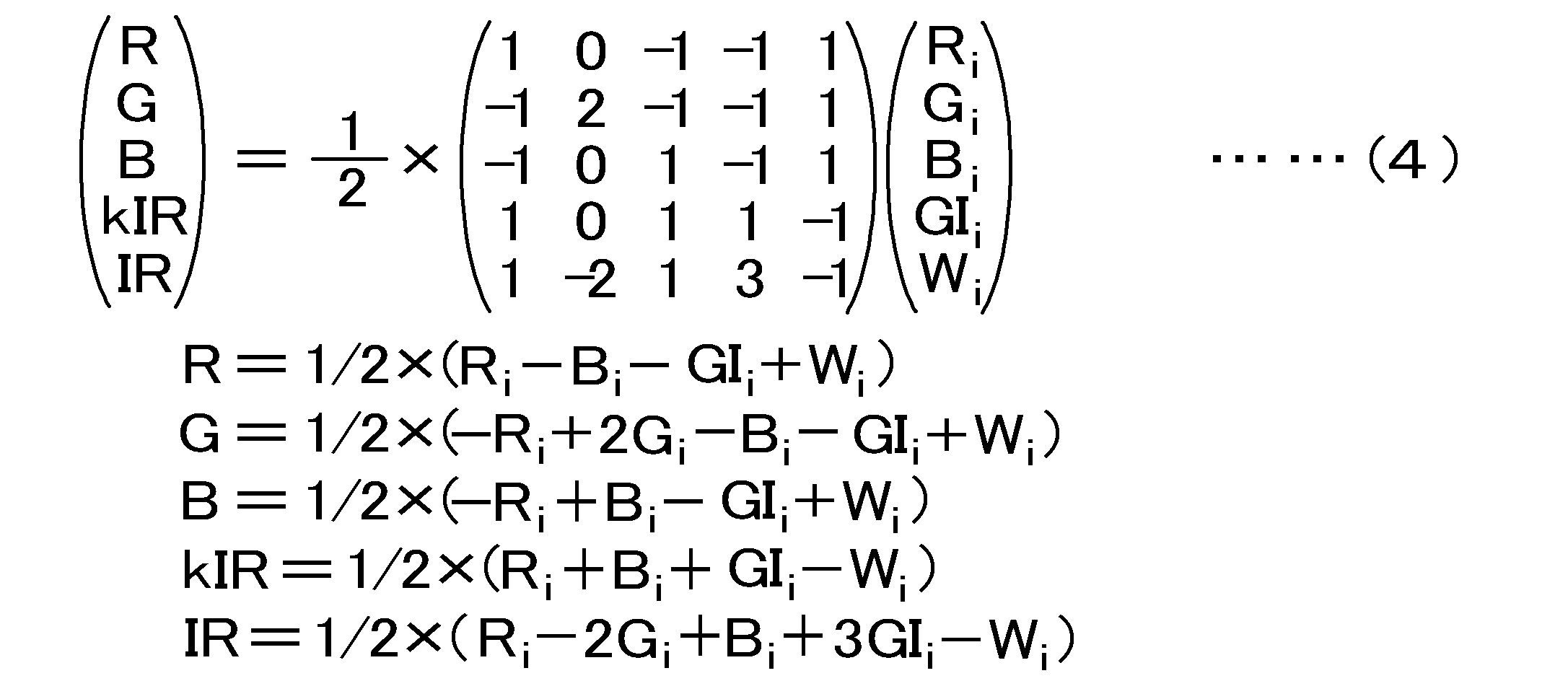
上述した実施例1によれば、選択的赤外光遮断フィルタの赤外光透過率k、もしくは、赤外光透過率kが乗算された赤外光成分kIRも単位画素配列毎に求めることができるため、先述した従来例に係るR,G,B,Wカラーフィルタ配列で問題となった、選択的赤外光遮断フィルタの赤外光透過率kの空間的、時間的な変動に影響されることなく、より高い精度で可視光と赤外光成分とを分離算出することが可能となる。また、従来例に係るR,G,B,Wカラーフィルタ配列で問題となった、解の発散の問題も回避することが可能となる。
(実施例1の変形例)
実施例1に係るカラーフィルタ配列と同様な効果は、単位画素配列を構成する各色(IR(赤外光)、全光(W)透過画素を含む)の画素において、選択的赤外光遮断フィルタの有り、無しの画素を備え、式(3)に対応する変換マトリクスが逆行列を持てば(行列式det≠0)、他の配列でも得ることが可能である。4行×4列繰り返しのカラーフィルタ配列の変形例を図5A及び図5Bに示し、2行×2列繰り返しのカラーフィルタ配列の変形例を図6A、図6B、図7A、及び、図7Bに示す。
実施例1に係るカラーフィルタ配列と同様な効果は、単位画素配列を構成する各色(IR(赤外光)、全光(W)透過画素を含む)の画素において、選択的赤外光遮断フィルタの有り、無しの画素を備え、式(3)に対応する変換マトリクスが逆行列を持てば(行列式det≠0)、他の配列でも得ることが可能である。4行×4列繰り返しのカラーフィルタ配列の変形例を図5A及び図5Bに示し、2行×2列繰り返しのカラーフィルタ配列の変形例を図6A、図6B、図7A、及び、図7Bに示す。
・第1変形例
実施例1の第1変形例に係るカラーフィルタ配列を図5Aに示す。第1変形例に係るカラーフィルタ配列は、実施例1に係るカラーフィルタ配列(図3A参照)において、GI画素をG画素に置き換え、3行3列目のR画素を、選択的赤外光遮断フィルタが形成されていないRI画素に置き換えた構成となっている。RI画素は、Rの波長帯域、及び、デュアルバンドパスフィルタ22を透過する赤外光の波長帯域の2つの波長帯域に感度をもつR画素である。
実施例1の第1変形例に係るカラーフィルタ配列を図5Aに示す。第1変形例に係るカラーフィルタ配列は、実施例1に係るカラーフィルタ配列(図3A参照)において、GI画素をG画素に置き換え、3行3列目のR画素を、選択的赤外光遮断フィルタが形成されていないRI画素に置き換えた構成となっている。RI画素は、Rの波長帯域、及び、デュアルバンドパスフィルタ22を透過する赤外光の波長帯域の2つの波長帯域に感度をもつR画素である。
・第2変形例
実施例1の第2変形例に係るカラーフィルタ配列を図5Bに示す。第2変形例に係るカラーフィルタ配列は、実施例1に係るカラーフィルタ配列(図3A参照)において、GI画素をG画素に置き換え、3行1列目のB画素を、選択的赤外光遮断フィルタが形成されていないBI画素に置き換えた構成となっている。BI画素は、Bの波長帯域、及び、デュアルバンドパスフィルタ22を透過する赤外光の波長帯域の2つの波長帯域に感度をもつB画素である。
実施例1の第2変形例に係るカラーフィルタ配列を図5Bに示す。第2変形例に係るカラーフィルタ配列は、実施例1に係るカラーフィルタ配列(図3A参照)において、GI画素をG画素に置き換え、3行1列目のB画素を、選択的赤外光遮断フィルタが形成されていないBI画素に置き換えた構成となっている。BI画素は、Bの波長帯域、及び、デュアルバンドパスフィルタ22を透過する赤外光の波長帯域の2つの波長帯域に感度をもつB画素である。
・第3変形例
実施例1の第3変形例に係るカラーフィルタ配列を図6Aに示す。第3変形例に係るカラーフィルタ配列は、R,W,G,Bの2行×2列の画素単位と、R,W,GI,Bの2行×2列の画素単位とが交互に配置された単位画素配列の構成となっている。GI画素は、Gの波長帯域、及び、デュアルバンドパスフィルタ22を透過する赤外光の波長帯域の2つの波長帯域に感度をもつ画素である。
実施例1の第3変形例に係るカラーフィルタ配列を図6Aに示す。第3変形例に係るカラーフィルタ配列は、R,W,G,Bの2行×2列の画素単位と、R,W,GI,Bの2行×2列の画素単位とが交互に配置された単位画素配列の構成となっている。GI画素は、Gの波長帯域、及び、デュアルバンドパスフィルタ22を透過する赤外光の波長帯域の2つの波長帯域に感度をもつ画素である。
・第4変形例
実施例1の第4変形例に係るカラーフィルタ配列を図6Bに示す。第4変形例に係るカラーフィルタ配列は、R,W,G,Bの2行×2列の画素単位と、RI,W,G,Bの2行×2列の画素単位とが交互に配置された単位画素配列の構成となっている。RI画素は、Rの波長帯域、及び、デュアルバンドパスフィルタ22を透過する赤外光の波長帯域の2つの波長帯域に感度をもつR画素である。
実施例1の第4変形例に係るカラーフィルタ配列を図6Bに示す。第4変形例に係るカラーフィルタ配列は、R,W,G,Bの2行×2列の画素単位と、RI,W,G,Bの2行×2列の画素単位とが交互に配置された単位画素配列の構成となっている。RI画素は、Rの波長帯域、及び、デュアルバンドパスフィルタ22を透過する赤外光の波長帯域の2つの波長帯域に感度をもつR画素である。
・第5変形例
実施例1の第5変形例に係るカラーフィルタ配列を図7Aに示す。第5変形例に係るカラーフィルタ配列は、R,W,G,Bの2行×2列の画素単位と、R,W,G,BIの2行×2列の画素単位とが交互に配置された単位画素配列の構成となっている。BI画素は、Bの波長帯域、及び、デュアルバンドパスフィルタ22を透過する赤外光の波長帯域の2つの波長帯域に感度をもつB画素である。
実施例1の第5変形例に係るカラーフィルタ配列を図7Aに示す。第5変形例に係るカラーフィルタ配列は、R,W,G,Bの2行×2列の画素単位と、R,W,G,BIの2行×2列の画素単位とが交互に配置された単位画素配列の構成となっている。BI画素は、Bの波長帯域、及び、デュアルバンドパスフィルタ22を透過する赤外光の波長帯域の2つの波長帯域に感度をもつB画素である。
・第6変形例
実施例1の第6変形例に係るカラーフィルタ配列を図7Bに示す。第6変形例に係るカラーフィルタ配列は、R,W,G,Bの2行×2列の画素単位と、R,WS,G,Bの2行×2列の画素単位とが交互に配置された単位画素配列の構成となっている。WS画素は、選択的赤外光遮断フィルタが形成されたW画素である。
実施例1の第6変形例に係るカラーフィルタ配列を図7Bに示す。第6変形例に係るカラーフィルタ配列は、R,W,G,Bの2行×2列の画素単位と、R,WS,G,Bの2行×2列の画素単位とが交互に配置された単位画素配列の構成となっている。WS画素は、選択的赤外光遮断フィルタが形成されたW画素である。
[実施例2]
実施例2は、R,G,B,Wの画素配列をベースとするカラーフィルタ配列において、W画素の半分を、Gの波長帯域、及び、デュアルバンドパスフィルタ22を透過する赤外光の波長帯域の2つの波長帯域に感度をもつGI画素に置き換えた例である。実施例2に係るカラーフィルタ配列を図8Aに示す。
実施例2は、R,G,B,Wの画素配列をベースとするカラーフィルタ配列において、W画素の半分を、Gの波長帯域、及び、デュアルバンドパスフィルタ22を透過する赤外光の波長帯域の2つの波長帯域に感度をもつGI画素に置き換えた例である。実施例2に係るカラーフィルタ配列を図8Aに示す。
図8Aに示すように、実施例2に係るカラーフィルタ配列では、4行×4列の画素配列において、1行目が、R画素、GI画素、B画素、GI画素から成り、2行目及び4行目が、W画素、G画素、W画素、G画素から成り、3行目がG画素、GI画素、R画素、GI画素から成る構成となっている。ここで、R画素、G画素、B画素は、選択的赤外光遮断フィルタが形成されている画素であり、GI画素、W画素は、選択的赤外光遮断フィルタが形成されていない画素である。実施例2に係るカラーフィルタ配列の変換マトリクス演算式は実施例1の場合と同じである。
実施例1では、G画素の半分をGI画素に置き換えている。実施例1の場合、赤外光の強度が強いときにGI画素から算出されるG信号のノイズが増大するため、カラー画像の品質に影響を与える場合がある。これに対し、実施例2に係るカラーフィルタ配列では、R,G,B画素のカラーフィルタ構成については、従来例に係るR,G,B,Wカラーフィルタ配列(図2B参照)と同様であるため、赤外光の強度が強いときでも、カラー画像の品質はそのまま保持することが可能である。
上述した実施例2によれば、実施例1の場合と同様に、選択的赤外光遮断フィルタの透過率kの空間的、時間的な変動に影響されることなく、より高い精度で可視光と赤外光成分とを分離算出することが可能となることに加えて、赤外光の強度が強いときでも、カラー画像の品質はそのまま保持することが可能となる。
(実施例2の変形例)
実施例2の変形例に係るカラーフィルタ配列を図8Bに示す。実施例2の変形例に係るカラーフィルタ配列は、R,G,B,Wの画素配列をベースとする4行×4列繰り返しのカラーフィルタ配列において、W画素の半分を、W画素に選択的赤外光遮断フィルタ232が形成されたWS画素に置き換えた例である。
実施例2の変形例に係るカラーフィルタ配列を図8Bに示す。実施例2の変形例に係るカラーフィルタ配列は、R,G,B,Wの画素配列をベースとする4行×4列繰り返しのカラーフィルタ配列において、W画素の半分を、W画素に選択的赤外光遮断フィルタ232が形成されたWS画素に置き換えた例である。
実施例2の変形例に係るカラーフィルタ配列において、各画素が発する信号強度をRi,Gi,Bi,WSi,Wiとすると、各色成分の強度と各画素の信号強度との関係は、次式(5)に示すようなマトリクス演算で表現される。

そして、次式(6)に示すように、変換マトリクスの逆行列を求め、逆変換を行うことにより、各画素の信号強度から、R,G,B,kIR,IRの各信号成分を分離算出することが可能になる。

実施例2に係るカラーフィルタ配列では、W画素の半分をGI画素に置き換えているため、可視光(R,B)の成分に対しては感度が落ちてしまう。これに対し、実施例2の変形例に係るカラーフィルタ配列では、W画素の半分をWS画素に置き換えているため、可視光(R,G,B)の成分に対して感度を維持することが可能となる。
[実施例3]
実施例3は、R,G,B-IR(赤外光)の画素配列を基本とする2行×2列繰り返しのカラーフィルタ配列の例である。実施例3に係るカラーフィルタ配列を図9に示す。
実施例3は、R,G,B-IR(赤外光)の画素配列を基本とする2行×2列繰り返しのカラーフィルタ配列の例である。実施例3に係るカラーフィルタ配列を図9に示す。
実施例3に係るカラーフィルタ配列において、実施例1に係るカラーフィルタ配列との差異は、図9から明らかなように、W画素が存在しないことである。すなわち、実施例3では、W画素をIR画素に置き換えた画素配列となっており、当該4行×4列の画素配列を単位として、各フィルタが画素アレイ部の各画素上に繰り返し展開される。IR画素は、赤外光の波長帯域を透過する透過特性を有する画素である。
実施例3に係るカラーフィルタ配列では、R,G,Bの各画素の上に選択的赤外光遮断フィルタを形成するとともに、当該カラーフィルタ配列に存在する4つのG画素のうち、2つのG画素には選択的赤外光遮断フィルタを形成し、他の2つのG画素(即ち、GI画素)には選択的赤外光遮断フィルタを形成しない構成となっている。
具体的には、図9に示すように、実施例3では、4行×4列の画素配列において、1行目が、R画素、GI画素、R画素、G画素から成り、2行目及び4行目が、IR画素、B画素、IR画素、B画素から成り、3行目がR画素、G画素、R画素、GI画素から成る構成となっている。ここで、R画素、G画素、B画素、IR画素は、選択的赤外光遮断フィルタが形成されている画素であり、GI画素は、選択的赤外光遮断フィルタが形成されていない画素である。
上記の実施例3に係るカラーフィルタ配列において、R,G,Bの各画素は、可視光である第1の色光(赤色光)、第2の色光(緑色光)、第3の色光(青色光)に対応する波長帯域を透過する各フィルタ、及び、選択的赤外光遮断フィルタを有する第1、第2、第3の画素である。IR画素は、赤外光の波長帯域を透過する透過特性を有する第4の画素である。GI画素は、第1の画素、第2の画素、第3の画素、及び、第4の画素のいずれとも異なる波長透過特性を有する第5の画素である。
実施例3に係るカラーフィルタ配列において、各画素が発する信号強度をRi,Gi,Bi,GIi,IRiとすると、各色成分の強度と各画素の信号強度との関係は、次式(7)に示すようなマトリクス演算で表現される。実施例1の場合と同様に、選択的赤外光遮断フィルタの赤外光透過率kを赤外光の強度に乗じたkIRも未知数とすることにより、5行×5列の変換式となる。

そして、次式(8)に示すように、変換マトリクスの逆行列を求め、逆変換を行うことにより、各画素の信号強度から、選択的赤外光遮断フィルタの赤外光透過率kも含め、R,G,B,kIR,IRの各信号成分を分離算出することが可能になる。

上述したR,G,B-IRの画素配列を基本とする実施例3においても、R,G,B,Wの画素配列を基本とする実施例1の場合と同様の作用、効果を得ることができる。すなわち、選択的赤外光遮断フィルタの赤外光透過率k、もしくは、赤外光透過率kが乗算された赤外光成分kIRも単位画素配列毎に求めることができるため、選択的赤外光遮断フィルタの赤外光透過率kの空間的、時間的な変動に影響されることなく、より高い精度で可視光と赤外光成分とを分離算出することが可能となる。
(実施例3の変形例)
実施例3に係るカラーフィルタ配列と同様な効果は、単位画素配列を構成する各色(IR(赤外光)画素を含む)の画素において、選択的赤外光遮断フィルタの有り、無しの画素を備え、式(7)に対応する変換マトリクスが逆行列を持てば(行列式det≠0)、他の配列でも得ることが可能である。
実施例3に係るカラーフィルタ配列と同様な効果は、単位画素配列を構成する各色(IR(赤外光)画素を含む)の画素において、選択的赤外光遮断フィルタの有り、無しの画素を備え、式(7)に対応する変換マトリクスが逆行列を持てば(行列式det≠0)、他の配列でも得ることが可能である。
・第1変形例
実施例3の第1変形例に係るカラーフィルタ配列を図10Aに示す。第1変形例に係るカラーフィルタ配列は、実施例3に係るカラーフィルタ配列(図9参照)において、3行1列目及び1行3列目の各R画素を、選択的赤外光遮断フィルタが形成されていないRI画素、即ち、Rの波長帯域、及び、デュアルバンドパスフィルタ22を透過する赤外光の波長帯域の2つの波長帯域に感度をもつRI画素に置き換えた構成となっている。
実施例3の第1変形例に係るカラーフィルタ配列を図10Aに示す。第1変形例に係るカラーフィルタ配列は、実施例3に係るカラーフィルタ配列(図9参照)において、3行1列目及び1行3列目の各R画素を、選択的赤外光遮断フィルタが形成されていないRI画素、即ち、Rの波長帯域、及び、デュアルバンドパスフィルタ22を透過する赤外光の波長帯域の2つの波長帯域に感度をもつRI画素に置き換えた構成となっている。
・第2変形例
実施例3の第2変形例に係るカラーフィルタ配列を図10Bに示す。第2変形例に係るカラーフィルタ配列は、実施例3に係るカラーフィルタ配列(図9参照)において、4行2列目及び2行4列目の各B画素を、選択的赤外光遮断フィルタが形成されていないBI画素、即ち、Bの波長帯域、及び、デュアルバンドパスフィルタ22を透過する赤外光の波長帯域の2つの波長帯域に感度をもつBI画素に置き換えた構成となっている。
実施例3の第2変形例に係るカラーフィルタ配列を図10Bに示す。第2変形例に係るカラーフィルタ配列は、実施例3に係るカラーフィルタ配列(図9参照)において、4行2列目及び2行4列目の各B画素を、選択的赤外光遮断フィルタが形成されていないBI画素、即ち、Bの波長帯域、及び、デュアルバンドパスフィルタ22を透過する赤外光の波長帯域の2つの波長帯域に感度をもつBI画素に置き換えた構成となっている。
[実施例4]
実施例4は、R,G,B-IRの画素配列をベースとする4行×4列繰り返しのカラーフィルタ配列において、解像度に効果が高いG画素の数を増やし、解像度に効果が低いR画素及びB画素の数を減らした例である。実施例4に係るカラーフィルタ配列を図11に示す。
実施例4は、R,G,B-IRの画素配列をベースとする4行×4列繰り返しのカラーフィルタ配列において、解像度に効果が高いG画素の数を増やし、解像度に効果が低いR画素及びB画素の数を減らした例である。実施例4に係るカラーフィルタ配列を図11に示す。
図11に示すように、実施例4では、R,G,B-IRの画素配列において、4行×4列の計16個の画素うち、半分の8個がG画素で、その8個のG画素のうち、4個のG画素には選択的赤外光遮断フィルタを形成し、他の4個のG画素には選択的赤外光遮断フィルタを形成しない構成となっている。そして、実施例3の場合の同様の変換式により、各フィルタの信号値を算出することが可能となる。
具体的には、4行×4列の画素配列において、1行目が、R画素、G画素、B画素、G画素から成り、2行目及び4行目が、GI画素、IR画素、GI画素、IR画素から成り、3行目が、B画素、G画素、R画素、G画素から成る構成となっている。ここで、R画素、G画素、B画素、IR画素は、選択的赤外光遮断フィルタが形成されている画素であり、GI画素は、選択的赤外光遮断フィルタが形成されていない画素である。
上述した実施例4によれば、R,G,B-IRの画素配列を基本としているため、実施例3の場合と同様の作用、効果を得ることができる。この作用、効果に加えて、実施例4では、解像度に効果が高いG画素の数が、R画素及びB画素の数よりも多いため、高解像度化を図ることができる。
(実施例4の変形例)
実施例4に係るカラーフィルタ配列と同様な効果は、単位画素配列を構成する各色(IR(赤外光)画素を含む)の画素において、選択的赤外光遮断フィルタの有り、無しの画素を備え、式(7)に対応する変換マトリクスが逆行列を持てば(行列式det≠0)、他の配列でも得ることが可能である。
実施例4に係るカラーフィルタ配列と同様な効果は、単位画素配列を構成する各色(IR(赤外光)画素を含む)の画素において、選択的赤外光遮断フィルタの有り、無しの画素を備え、式(7)に対応する変換マトリクスが逆行列を持てば(行列式det≠0)、他の配列でも得ることが可能である。
・第1変形例
実施例4の第1変形例に係るカラーフィルタ配列を図12Aに示す。第1変形例に係るカラーフィルタ配列は、実施例4に係るカラーフィルタ配列(図11参照)において、GI画素をG画素に置き換えるとともに、3行3列目のR画素を、選択的赤外光遮断フィルタが形成されていないRI画素に置き換えた構成となっている。
実施例4の第1変形例に係るカラーフィルタ配列を図12Aに示す。第1変形例に係るカラーフィルタ配列は、実施例4に係るカラーフィルタ配列(図11参照)において、GI画素をG画素に置き換えるとともに、3行3列目のR画素を、選択的赤外光遮断フィルタが形成されていないRI画素に置き換えた構成となっている。
・第2変形例
実施例4の第2変形例に係るカラーフィルタ配列を図12Bに示す。第1変形例に係るカラーフィルタ配列は、実施例4に係るカラーフィルタ配列(図11参照)において、GI画素をG画素に置き換えるとともに、3行1列目のB画素を、選択的赤外光遮断フィルタが形成されていないGI画素に置き換えた構成となっている。
実施例4の第2変形例に係るカラーフィルタ配列を図12Bに示す。第1変形例に係るカラーフィルタ配列は、実施例4に係るカラーフィルタ配列(図11参照)において、GI画素をG画素に置き換えるとともに、3行1列目のB画素を、選択的赤外光遮断フィルタが形成されていないGI画素に置き換えた構成となっている。
[実施例5]
実施例5は、R,G,B-IRの画素配列をベースとする4行×4列繰り返しのカラーフィルタ配列において、G画素の半分を、選択的赤外光遮断フィルタが形成されたWS画素に置き換えた例である。実施例5に係るカラーフィルタ配列を図13Aに示す。
実施例5は、R,G,B-IRの画素配列をベースとする4行×4列繰り返しのカラーフィルタ配列において、G画素の半分を、選択的赤外光遮断フィルタが形成されたWS画素に置き換えた例である。実施例5に係るカラーフィルタ配列を図13Aに示す。
図13Aに示すように、実施例5に係るカラーフィルタ配列は、R,G,B-IRの画素配列において、G画素の半分をWS画素に置き換えるとともに、G画素、WS画素、及び、IR画素が4個ずつ配置された構成となっている。具体的には、4行×4列の画素配列において、1行目が、R画素、G画素、B画素、G画素から成り、2行目及び4行目が、WS画素、IR画素、WS画素、IR画素から成り、3行目が、B画素、G画素、R画素、G画素から成る構成となっている。WS画素は、選択的赤外光遮断フィルタが形成されたW画素である。
上記の実施例5に係るカラーフィルタ配列において、R,G,Bの各画素は、可視光である第1の色光(赤色光)、第2の色光(緑色光)、第3の色光(青色光)に対応する波長帯域を透過する各フィルタ、及び、選択的赤外光遮断フィルタを有する第1、第2、第3の画素である。IR画素は、赤外光の波長帯域を透過する透過特性を有する第4の画素である。WS画素は、第1の画素、第2の画素、第3の画素、及び、第4の画素のいずれとも異なる波長透過特性を有する第5の画素である。
実施例5に係るカラーフィルタ配列において、各画素が発する信号強度をRi,Gi,Bi,WSi,IRiとすると、各色成分の強度と各画素の信号強度との関係は、次式(9)に示すようなマトリクス演算で表現される。

そして、次式(10)に示すように、変換マトリクスの逆行列を求め、逆変換を行うことにより、各画素の信号強度から、選択的赤外光遮断フィルタの赤外光透過率kも含め、R,G,B,kIR,IRの各信号成分を分離算出することが可能になる。

上述した実施例5においても、R,G,B-IRの画素配列を基本としているため、実施例3の場合と同様の作用、効果を得ることができる。また、実施例5の場合、G画素の半分をWS画素に置き換えているため、実施例4に比べて赤外光の解像度が減少するものの、可視光の感度の向上を図ることができる。
(実施例5の変形例)
実施例5の変形例に係るカラーフィルタ配列を図13Bに示す。図13Bに示すように、実施例5の変形例では、実施例5の画素配列(図13A)に対して、2行目、4行目の色配列が異なっている。具体的には、実施例5の画素配列では、2行目及び4行目が共にWS画素、IR画素、WS画素、IR画素の配列となっている。これに対して、実施例5の変形例の画素配列では、2行目がWS画素、B画素、IR画素、B画素の配列となり、4行目がIR画素、B画素、WS画素、B画素の配列となっている。
実施例5の変形例に係るカラーフィルタ配列を図13Bに示す。図13Bに示すように、実施例5の変形例では、実施例5の画素配列(図13A)に対して、2行目、4行目の色配列が異なっている。具体的には、実施例5の画素配列では、2行目及び4行目が共にWS画素、IR画素、WS画素、IR画素の配列となっている。これに対して、実施例5の変形例の画素配列では、2行目がWS画素、B画素、IR画素、B画素の配列となり、4行目がIR画素、B画素、WS画素、B画素の配列となっている。
[実施例6]
実施例6は、R,G,B-IRの画素配列をベースとするカラーフィルタ配列において、IR画素の半分を、IR画素に選択的赤外光遮断フィルタが形成されたkIR画素に置き換えた例である。実施例6に係るカラーフィルタ配列を図14Aに示す。
実施例6は、R,G,B-IRの画素配列をベースとするカラーフィルタ配列において、IR画素の半分を、IR画素に選択的赤外光遮断フィルタが形成されたkIR画素に置き換えた例である。実施例6に係るカラーフィルタ配列を図14Aに示す。
実施例6に係るカラーフィルタ配列は、4行×4列の画素配列において、1行目及び3行目が、R画素、G画素、B画素、G画素から成り、2行目が、kIR画素、B画素、IR画素、B画素から成り、4行目が、IR画素、kIR画素、R画素、B画素から成る構成となっている。
上記の実施例6に係るカラーフィルタ配列において、R,G,Bの各画素は、可視光である第1の色光(赤色光)、第2の色光(緑色光)、第3の色光(青色光)に対応する波長帯域を透過する各フィルタ、及び、選択的赤外光遮断フィルタを有する第1、第2、第3の画素である。IR画素は、赤外光の波長帯域を透過する透過特性を有する第4の画素である。kIR画素は、第1の画素、第2の画素、第3の画素、及び、第4の画素のいずれとも異なる波長透過特性を有する第5の画素である。
実施例6に係るカラーフィルタ配列において、各画素が発する信号強度をRi,Gi,Bi,kIRi,IRiとすると、各色成分の強度と各画素の信号強度との関係は、次式(11)に示すようなマトリクス演算で表現される。

そして、次式(12)に示すように、変換マトリクスの逆行列を求め、逆変換を行うことにより、各画素の信号強度から、選択的赤外光遮断フィルタの赤外光透過率kも含め、R,G,B,kIR,IRの各信号成分を分離算出することが可能になる。

上述した実施例6においても、R,G,B-IRの画素配列を基本としているため、実施例3の場合と同様の作用、効果を得ることができる。また、IR画素の半分をkIR画素に置き換えているため、赤外光の解像度は劣化するものの、IR画素及びkIR画素で選択的赤外光遮断フィルタの赤外光透過率kを算出することが可能になる。
(実施例6の変形例)
実施例6の変形例に係るカラーフィルタ配列を図14Bに示す。本変形例に係るカラーフィルタ配列では、4行×4列の画素配列において、1行目が、R画素、G画素、B画素、G画素から成り、2行目が、G画素、kIR画素、G画素、IR画素から成り、3行目が、B画素、G画素、IR画素、G画素から成り、4行目が、G画素、IR画素、G画素、kIR画素から成る構成となっている。
実施例6の変形例に係るカラーフィルタ配列を図14Bに示す。本変形例に係るカラーフィルタ配列では、4行×4列の画素配列において、1行目が、R画素、G画素、B画素、G画素から成り、2行目が、G画素、kIR画素、G画素、IR画素から成り、3行目が、B画素、G画素、IR画素、G画素から成り、4行目が、G画素、IR画素、G画素、kIR画素から成る構成となっている。
[実施例7]
実施例7は、R,G,B-W,IRの画素配列を基本とするカラーフィルタ配列の例である。実施例7に係るカラーフィルタ配列を図15に示す。
実施例7は、R,G,B-W,IRの画素配列を基本とするカラーフィルタ配列の例である。実施例7に係るカラーフィルタ配列を図15に示す。
実施例7に係るカラーフィルタ配列では、実施例4に係るR,G,B-IRの画素配列(図11参照)に対し、IR画素の半分をW画素に置き換えた構成となっている。具体的には、実施例7に係るカラーフィルタ配列は、R,G,G,IRの2行×2列の画素単位と、B,G,G,Wの2行×2列の画素単位とが交互に配置された単位画素配列の構成となっている。
実施例7に係るカラーフィルタ配列において、各画素が発する信号強度をRi,Gi,Bi,Wi,IRiとすると、各色成分の強度と各画素の信号強度との関係は、次式(13)に示すようなマトリクス演算で表現される。

そして、次式(14)に示すように、変換マトリクスの逆行列を求め、逆変換を行うことにより、各画素の信号強度から、選択的赤外光遮断フィルタの赤外光透過率kも含め、R,G,B,kIR,IRの各信号成分を分離算出することが可能になる。

上述したR,G,B-W,IRの画素配列を基本とする実施例7においても、R,G,B,Wの画素配列を基本とする実施例1や、R,G,B-IRの画素配列を基本とする実施例3の場合と同様の作用、効果を得ることができる。すなわち、選択的赤外光遮断フィルタの赤外光透過率k、もしくは、赤外光透過率kが乗算された赤外光成分kIRも単位画素配列毎に求めることができるため、選択的赤外光遮断フィルタの赤外光透過率kの空間的、時間的な変動に影響されることなく、より高い精度で可視光と赤外光成分とを分離算出することが可能となる。
(実施例7の変形例)
実施例7に係るカラーフィルタ配列と同様な効果は、単位画素配列を構成する各色(IR画素、W画素を含む)の画素において、選択的赤外光遮断フィルタの有り、無しの画素を備え、式(13)に対応する変換マトリクスが逆行列を持てば(行列式det≠0)、他の配列でも得ることが可能である。
実施例7に係るカラーフィルタ配列と同様な効果は、単位画素配列を構成する各色(IR画素、W画素を含む)の画素において、選択的赤外光遮断フィルタの有り、無しの画素を備え、式(13)に対応する変換マトリクスが逆行列を持てば(行列式det≠0)、他の配列でも得ることが可能である。
・第1変形例
実施例7の第1変形例に係るカラーフィルタ配列を図16Aに示す。第1変形例に係るカラーフィルタ配列は、R,IR,G,Bの2行×2列の画素単位と、R,W,G,Bの2行×2列の画素単位とが交互に配置された単位画素配列の構成となっている。
実施例7の第1変形例に係るカラーフィルタ配列を図16Aに示す。第1変形例に係るカラーフィルタ配列は、R,IR,G,Bの2行×2列の画素単位と、R,W,G,Bの2行×2列の画素単位とが交互に配置された単位画素配列の構成となっている。
・第2変形例
実施例7の第2変形例に係るカラーフィルタ配列を図16Bに示す。第2変形例に係るカラーフィルタ配列は、R,kIR,G,Bの2行×2列の画素単位と、R,W,G,Bの2行×2列の画素単位とが交互に配置された単位画素配列の構成となっている。
実施例7の第2変形例に係るカラーフィルタ配列を図16Bに示す。第2変形例に係るカラーフィルタ配列は、R,kIR,G,Bの2行×2列の画素単位と、R,W,G,Bの2行×2列の画素単位とが交互に配置された単位画素配列の構成となっている。
[実施例8]
実施例8も、実施例7と同様に、R,G,B-W,IRの画素配列を基本とするカラーフィルタ配列の例である。実施例8に係るカラーフィルタ配列を図17に示す。
実施例8も、実施例7と同様に、R,G,B-W,IRの画素配列を基本とするカラーフィルタ配列の例である。実施例8に係るカラーフィルタ配列を図17に示す。
実施例8に係るカラーフィルタ配列では、R,G,B,Wの画素配列に対し、G画素の半分をIR画素に置き換えた構成となっている。具体的には、R,W,W,IRの2行×2列の画素単位と、B,W,W,Gの2行×2列の画素単位とが交互に配置された単位画素配列の構成となっている。実施例8に係るカラーフィルタ配列の変換マトリクス演算式は実施例7の場合と同じである。
上述したR,G,B-W,IRの画素配列を基本とする実施例8においても、R,G,B,Wの画素配列を基本とする実施例1や、R,G,B-IRの画素配列を基本とする実施例3の場合と同様の作用、効果を得ることができる。すなわち、選択的赤外光遮断フィルタの赤外光透過率k、もしくは、赤外光透過率kが乗算された赤外光成分kIRも単位画素配列毎に求めることができるため、選択的赤外光遮断フィルタの赤外光透過率kの空間的、時間的な変動に影響されることなく、より高い精度で可視光と赤外光成分とを分離算出することが可能となる。
(実施例8の変形例)
実施例8に係るカラーフィルタ配列と同様な効果は、単位画素配列を構成する各色(IR画素、W画素を含む)の画素において、選択的赤外光遮断フィルタの有り、無しの画素を備え、式(13)に対応する変換マトリクスが逆行列を持てば(行列式det≠0)、他の配列でも得ることが可能である。
実施例8に係るカラーフィルタ配列と同様な効果は、単位画素配列を構成する各色(IR画素、W画素を含む)の画素において、選択的赤外光遮断フィルタの有り、無しの画素を備え、式(13)に対応する変換マトリクスが逆行列を持てば(行列式det≠0)、他の配列でも得ることが可能である。
・第1変形例
実施例8の第1変形例に係るカラーフィルタ配列を図18Aに示す。第1変形例に係るカラーフィルタ配列は、実施例8に係るカラーフィルタ配列(図17参照)において、IR画素をG画素に、W画素の半分をIR画素に置き換えた構成となっている。具体的には、第1変形例に係るカラーフィルタ配列は、R,W,IR,Gの2行×2列の画素単位と、B,W,IR,Gの2行×2列の画素単位とが交互に配置された単位画素配列の構成となっている。
実施例8の第1変形例に係るカラーフィルタ配列を図18Aに示す。第1変形例に係るカラーフィルタ配列は、実施例8に係るカラーフィルタ配列(図17参照)において、IR画素をG画素に、W画素の半分をIR画素に置き換えた構成となっている。具体的には、第1変形例に係るカラーフィルタ配列は、R,W,IR,Gの2行×2列の画素単位と、B,W,IR,Gの2行×2列の画素単位とが交互に配置された単位画素配列の構成となっている。
・第2変形例
実施例7の第2変形例に係るカラーフィルタ配列を図18Bに示す。第2変形例に係るカラーフィルタ配列は、実施例8に係るカラーフィルタ配列(図17参照)において、IR画素をG画素に、W画素の半分をkIR画素に置き換えた構成となっている。具体的には、第2変形例に係るカラーフィルタ配列は、R,W,kIR,Gの2行×2列の画素単位と、B,W,kIR,Gの2行×2列の画素単位とが交互に配置された単位画素配列の構成となっている。
実施例7の第2変形例に係るカラーフィルタ配列を図18Bに示す。第2変形例に係るカラーフィルタ配列は、実施例8に係るカラーフィルタ配列(図17参照)において、IR画素をG画素に、W画素の半分をkIR画素に置き換えた構成となっている。具体的には、第2変形例に係るカラーフィルタ配列は、R,W,kIR,Gの2行×2列の画素単位と、B,W,kIR,Gの2行×2列の画素単位とが交互に配置された単位画素配列の構成となっている。
[実施例9]
実施例9は、R,B,W,WS-IRの画素配列を基本とするカラーフィルタ配列の例である。実施例9に係るカラーフィルタ配列を図19Aに示す。
実施例9は、R,B,W,WS-IRの画素配列を基本とするカラーフィルタ配列の例である。実施例9に係るカラーフィルタ配列を図19Aに示す。
実施例9に係るカラーフィルタ配列では、実施例4に係るカラーフィルタ配列(図11参照)において、G画素をWS画素に、GI画素をW画素にそれぞれ置き換えた構成となっている。具体的には、実施例9に係るカラーフィルタ配列は、R,W,WS,IRの2行×2列の画素単位と、B,W,WS,IRの2行×2列の画素単位とが交互に配置された単位画素配列の構成となっている。G信号については、他の画素信号から算出することになる。
実施例9に係るカラーフィルタ配列において、各画素が発する信号強度をRi,Bi,WSi,Wi,IRiとすると、各色成分の強度と各画素の信号強度との関係は、次式(15)に示すようなマトリクス演算で表現される。
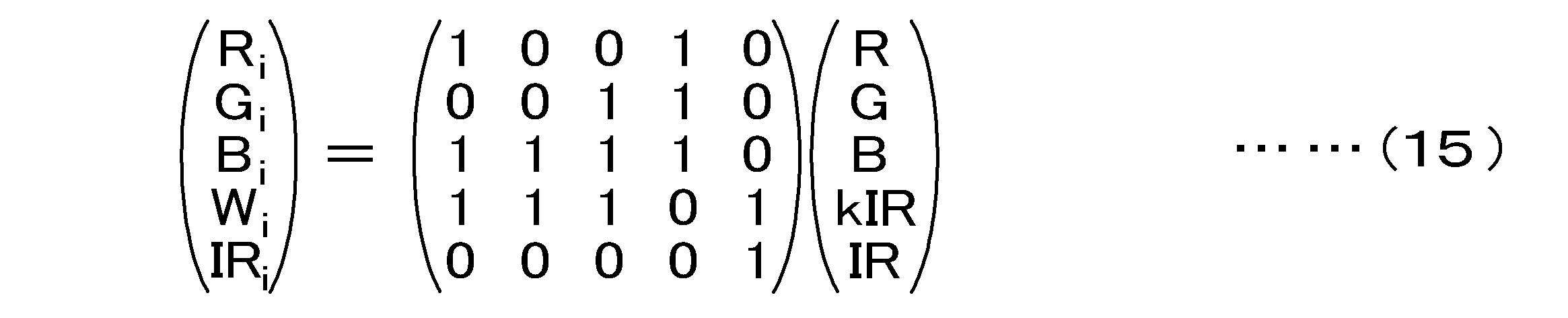
そして、次式(16)に示すように、変換マトリクスの逆行列を求め、逆変換を行うことにより、各画素の信号強度から、選択的赤外光遮断フィルタの赤外光透過率kも含め、R,G,B,kIR,IRの各信号成分を分離算出することが可能になる。

上述したR,B,W,WS-IRの画素配列を基本とする実施例9においても、選択的赤外光遮断フィルタの赤外光透過率k、もしくは、赤外光透過率kが乗算された赤外光成分kIRも単位画素配列毎に求めることができる。従って、選択的赤外光遮断フィルタの赤外光透過率kの空間的、時間的な変動に影響されることなく、より高い精度で可視光と赤外光成分とを分離算出することが可能となる。また、G画素をWS画素に、GI画素をW画素にそれぞれ置き換えたことで、置き換えない場合よりも感度の向上を図ることができる。
(実施例9の変形例)
実施例9に係るカラーフィルタ配列と同様な効果は、単位画素配列を構成する各色(IR画素、W画素を含む)の画素において、選択的赤外光遮断フィルタの有り、無しの画素を備え、式(15)に対応する変換マトリクスが逆行列を持てば(行列式det≠0)、他の配列でも得ることが可能である。
実施例9に係るカラーフィルタ配列と同様な効果は、単位画素配列を構成する各色(IR画素、W画素を含む)の画素において、選択的赤外光遮断フィルタの有り、無しの画素を備え、式(15)に対応する変換マトリクスが逆行列を持てば(行列式det≠0)、他の配列でも得ることが可能である。
・第1変形例
実施例9の第1変形例に係るカラーフィルタ配列を図19Bに示す。第1変形例に係るカラーフィルタ配列は、R,W,WS,Bの2行×2列の画素単位と、R,IR,WS,Bの2行×2列の画素単位とが交互に配置された単位画素配列の構成となっている。
実施例9の第1変形例に係るカラーフィルタ配列を図19Bに示す。第1変形例に係るカラーフィルタ配列は、R,W,WS,Bの2行×2列の画素単位と、R,IR,WS,Bの2行×2列の画素単位とが交互に配置された単位画素配列の構成となっている。
・第2変形例
実施例9の第2変形例に係るカラーフィルタ配列を図20Aに示す。第2変形例に係るカラーフィルタ配列は、第1変形例に係るカラーフィルタ配列(図19B参照)において、IR画素をkIR画素に置き換えた構成となっている。具体的には、第2変形例に係るカラーフィルタ配列は、R,W,WS,Bの2行×2列の画素単位と、R,kIR,WS,Bの2行×2列の画素単位とが交互に配置された単位画素配列の構成となっている。
実施例9の第2変形例に係るカラーフィルタ配列を図20Aに示す。第2変形例に係るカラーフィルタ配列は、第1変形例に係るカラーフィルタ配列(図19B参照)において、IR画素をkIR画素に置き換えた構成となっている。具体的には、第2変形例に係るカラーフィルタ配列は、R,W,WS,Bの2行×2列の画素単位と、R,kIR,WS,Bの2行×2列の画素単位とが交互に配置された単位画素配列の構成となっている。
・第3変形例
実施例9の第3変形例に係るカラーフィルタ配列を図20Bに示す。第3変形例に係るカラーフィルタ配列は、実施例9に係るカラーフィルタ配列(図19A参照)において、IR画素の半分をkIR画素に置き換えた構成となっている。具体的には、第3変形例に係るカラーフィルタ配列は、R,W,WS,IRの2行×2列の画素単位と、B,W,WS,kIRの2行×2列の画素単位とが交互に配置された単位画素配列の構成となっている。
実施例9の第3変形例に係るカラーフィルタ配列を図20Bに示す。第3変形例に係るカラーフィルタ配列は、実施例9に係るカラーフィルタ配列(図19A参照)において、IR画素の半分をkIR画素に置き換えた構成となっている。具体的には、第3変形例に係るカラーフィルタ配列は、R,W,WS,IRの2行×2列の画素単位と、B,W,WS,kIRの2行×2列の画素単位とが交互に配置された単位画素配列の構成となっている。
[実施例10]
実施例10は、R,G,Bのカラーフィルタを補色フィルタに置き換えたカラーフィルタ配列の例である。補色フィルタとしては、Ye(イエロー),Mg(マゼンタ),Cy(シアン)を例示することができる。実施例10に係るカラーフィルタ配列を図21Aに示す。
実施例10は、R,G,Bのカラーフィルタを補色フィルタに置き換えたカラーフィルタ配列の例である。補色フィルタとしては、Ye(イエロー),Mg(マゼンタ),Cy(シアン)を例示することができる。実施例10に係るカラーフィルタ配列を図21Aに示す。
実施例10に係るカラーフィルタ配列は、R,G,B-IRの画素配列をベースとするカラーフィルタ配列において、R,G,Bのうち、R画素の半分をYI画素に置き換えた構成となっている。具体的には、実施例10に係るカラーフィルタ配列は、R,IR,G,Bの2行×2列の画素単位と、YI,IR,G,Bの2行×2列の画素単位とが交互に配置された単位画素配列の構成となっている。ここで、YI画素は、選択的赤外光遮断フィルタが形成されていないYe画素である。
上記の実施例10に係るカラーフィルタ配列において、R,G,Bの各画素は、可視光である第1の色光(赤色光)、第2の色光(緑色光)、第3の色光(青色光)に対応する波長帯域を透過する各フィルタ、及び、選択的赤外光遮断フィルタ232を有する第1、第2、第3の画素である。IR画素は、赤外光の波長帯域を透過する透過特性を有する第4の画素である。補色画素であるYI画素は、第1の画素、第2の画素、第3の画素、及び、第4の画素のいずれとも異なる波長透過特性を有する第5の画素である。
実施例10に係るカラーフィルタ配列において、各画素が発する信号強度をRi,Gi,Bi,YIi,IRiとすると、各色成分の強度と各画素の信号強度との関係は、次式(17)に示すようなマトリクス演算で表現される。

そして、次式(18)に示すように、変換マトリクスの逆行列を求め、逆変換を行うことにより、各画素の信号強度から、選択的赤外光遮断フィルタの赤外光透過率kも含め、R,G,B,kIR,IRの各信号成分を分離算出することが可能になる。

上述したR,G,B-IRのカラーフィルタ配列において、R画素の半分をYI画素に置き換えた実施例10においても、選択的赤外光遮断フィルタの赤外光透過率k、もしくは、赤外光透過率kが乗算された赤外光成分kIRも単位画素配列毎に求めることができる。従って、選択的赤外光遮断フィルタの赤外光透過率kの空間的、時間的な変動に影響されることなく、より高い精度で可視光と赤外光成分とを分離算出することが可能となる。また、補色フィルタを使用する構成を採ることにより、R,G,Bのカラーフィルタを使用する場合に比べて、可視光の感度を上げることが可能になる。
(実施例10の変形例)
実施例10に係るカラーフィルタ配列と同様な効果は、単位画素配列を構成する各色(IR画素、YI画素を含む)の画素において、選択的赤外光遮断フィルタの有り、無しの画素を備え、式(17)に対応する変換マトリクスが逆行列を持てば(行列式det≠0)、他の配列でも得ることが可能である。
実施例10に係るカラーフィルタ配列と同様な効果は、単位画素配列を構成する各色(IR画素、YI画素を含む)の画素において、選択的赤外光遮断フィルタの有り、無しの画素を備え、式(17)に対応する変換マトリクスが逆行列を持てば(行列式det≠0)、他の配列でも得ることが可能である。
・第1変形例
実施例10の第1変形例に係るカラーフィルタ配列を図21Bに示す。第1変形例に係るカラーフィルタ配列は、実施例10に係るカラーフィルタ配列において(図21A参照)、YI画素をMI画素に置き換えた構成となっている。具体的には、第1変形例に係るカラーフィルタ配列は、R,IR,G,Bの2行×2列の画素単位と、MI,IR,G,Bの2行×2列の画素単位とが交互に配置された単位画素配列の構成となっている。ここで、補色画素であるMI画素は、選択的赤外光遮断フィルタが形成されていないMg画素であり、第1の画素、第2の画素、第3の画素、及び、第4の画素のいずれとも異なる波長透過特性を有する第5の画素である。
実施例10の第1変形例に係るカラーフィルタ配列を図21Bに示す。第1変形例に係るカラーフィルタ配列は、実施例10に係るカラーフィルタ配列において(図21A参照)、YI画素をMI画素に置き換えた構成となっている。具体的には、第1変形例に係るカラーフィルタ配列は、R,IR,G,Bの2行×2列の画素単位と、MI,IR,G,Bの2行×2列の画素単位とが交互に配置された単位画素配列の構成となっている。ここで、補色画素であるMI画素は、選択的赤外光遮断フィルタが形成されていないMg画素であり、第1の画素、第2の画素、第3の画素、及び、第4の画素のいずれとも異なる波長透過特性を有する第5の画素である。
・第2変形例
実施例10の第2変形例に係るカラーフィルタ配列を図22Aに示す。第2変形例に係るカラーフィルタ配列は、実施例10に係るカラーフィルタ配列において(図21A参照)、YI画素をCI画素に置き換えた構成となっている。具体的には、第2変形例に係るカラーフィルタ配列は、R,IR,G,Bの2行×2列の画素単位と、CI,IR,G,Bの2行×2列の画素単位とが交互に配置された単位画素配列の構成となっている。ここで、補色画素であるCI画素は、選択的赤外光遮断フィルタが形成されていないCy画素であり、第1の画素、第2の画素、第3の画素、及び、第4の画素のいずれとも異なる波長透過特性を有する第5の画素である。
実施例10の第2変形例に係るカラーフィルタ配列を図22Aに示す。第2変形例に係るカラーフィルタ配列は、実施例10に係るカラーフィルタ配列において(図21A参照)、YI画素をCI画素に置き換えた構成となっている。具体的には、第2変形例に係るカラーフィルタ配列は、R,IR,G,Bの2行×2列の画素単位と、CI,IR,G,Bの2行×2列の画素単位とが交互に配置された単位画素配列の構成となっている。ここで、補色画素であるCI画素は、選択的赤外光遮断フィルタが形成されていないCy画素であり、第1の画素、第2の画素、第3の画素、及び、第4の画素のいずれとも異なる波長透過特性を有する第5の画素である。
・第3変形例
実施例10の第3変形例に係るカラーフィルタ配列を図22Bに示す。第3変形例に係るカラーフィルタ配列は、実施例4に係るカラーフィルタ配列(図11参照)において、GI画素をYI画素に置き換えた構成となっている。具体的には、第3変形例に係るカラーフィルタ配列は、R,YI,G,IRの2行×2列の画素単位と、B,YI,G,IRの2行×2列の画素単位とが交互に配置された単位画素配列の構成となっている。
実施例10の第3変形例に係るカラーフィルタ配列を図22Bに示す。第3変形例に係るカラーフィルタ配列は、実施例4に係るカラーフィルタ配列(図11参照)において、GI画素をYI画素に置き換えた構成となっている。具体的には、第3変形例に係るカラーフィルタ配列は、R,YI,G,IRの2行×2列の画素単位と、B,YI,G,IRの2行×2列の画素単位とが交互に配置された単位画素配列の構成となっている。
・第4変形例
実施例10の第4変形例に係るカラーフィルタ配列を図23Aに示す。第4変形例に係るカラーフィルタ配列は、実施例4に係るカラーフィルタ配列(図11参照)において、GI画素をMI画素に置き換えた構成となっている。具体的には、第4変形例に係るカラーフィルタ配列は、R,MI,G,IRの2行×2列の画素単位と、B,MI,G,IRの2行×2列の画素単位とが交互に配置された単位画素配列の構成となっている。
実施例10の第4変形例に係るカラーフィルタ配列を図23Aに示す。第4変形例に係るカラーフィルタ配列は、実施例4に係るカラーフィルタ配列(図11参照)において、GI画素をMI画素に置き換えた構成となっている。具体的には、第4変形例に係るカラーフィルタ配列は、R,MI,G,IRの2行×2列の画素単位と、B,MI,G,IRの2行×2列の画素単位とが交互に配置された単位画素配列の構成となっている。
・第5変形例
実施例10の第5変形例に係るカラーフィルタ配列を図23Bに示す。第5変形例に係るカラーフィルタ配列は、実施例4に係るカラーフィルタ配列(図11参照)において、GI画素をCI画素に置き換えた構成となっている。具体的には、第5変形例に係るカラーフィルタ配列は、R,CI,G,IRの2行×2列の画素単位と、B,CI,G,IRの2行×2列の画素単位とが交互に配置された単位画素配列の構成となっている。
実施例10の第5変形例に係るカラーフィルタ配列を図23Bに示す。第5変形例に係るカラーフィルタ配列は、実施例4に係るカラーフィルタ配列(図11参照)において、GI画素をCI画素に置き換えた構成となっている。具体的には、第5変形例に係るカラーフィルタ配列は、R,CI,G,IRの2行×2列の画素単位と、B,CI,G,IRの2行×2列の画素単位とが交互に配置された単位画素配列の構成となっている。
[実施例11]
実施例11は、R,G,B-IRの画素配列をベースとするカラーフィルタ配列において、R,G,Bのうち、R画素の半分をYe画素に置き換えた例である。ここで、Ye画素は、選択的赤外光遮断フィルタが形成されている画素である。実施例11に係るカラーフィルタ配列を図24Aに示す。
実施例11は、R,G,B-IRの画素配列をベースとするカラーフィルタ配列において、R,G,Bのうち、R画素の半分をYe画素に置き換えた例である。ここで、Ye画素は、選択的赤外光遮断フィルタが形成されている画素である。実施例11に係るカラーフィルタ配列を図24Aに示す。
実施例11に係るカラーフィルタ配列は、実施例10に係るカラーフィルタ配列(図21A参照)において、YI画素をYe画素に置き換えた構成となっている。具体的には、実施例11に係るカラーフィルタ配列は、R,IR,G,Bの2行×2列の画素単位と、Ye,IR,G,Bの2行×2列の画素単位とが交互に配置された単位画素配列の構成となっている。Ye画素は選択的赤外光遮断フィルタが形成されている画素である。
実施例11に係るカラーフィルタ配列において、各画素が発する信号強度をRi,Gi,Bi,Yei,IRiとすると、各色成分の強度と各画素の信号強度との関係は、次式(19)に示すようなマトリクス演算で表現される。

そして、次式(20)に示すように、変換マトリクスの逆行列を求め、逆変換を行うことにより、各画素の信号強度から、選択的赤外光遮断フィルタの赤外光透過率kも含め、R,G,B,kIR,IRの各信号成分を分離算出することが可能になる。

上述した実施例11、即ち、R,G,B-IRのカラーフィルタ配列において、R画素の半分をYe画素に置き換えたカラーフィルタ配列においても、選択的赤外光遮断フィルタの赤外光透過率k、もしくは、赤外光透過率kが乗算された赤外光成分kIRも単位画素配列毎に求めることができる。従って、選択的赤外光遮断フィルタの赤外光透過率kの空間的、時間的な変動に影響されることなく、より高い精度で可視光と赤外光成分とを分離算出することが可能となる。また、実施例10の場合と同様に、補色フィルタを使用する構成を採ることにより、R,G,Bのカラーフィルタを使用する場合に比べて、可視光の感度を上げることが可能になる。
(実施例11の変形例)
実施例11に係るカラーフィルタ配列と同様な効果は、単位画素配列を構成する各色(IR画素、Ye画素を含む)の画素において、選択的赤外光遮断フィルタの有り、無しの画素を備え、式(19)に対応する変換マトリクスが逆行列を持てば(行列式det≠0)、他の配列でも得ることが可能である。
実施例11に係るカラーフィルタ配列と同様な効果は、単位画素配列を構成する各色(IR画素、Ye画素を含む)の画素において、選択的赤外光遮断フィルタの有り、無しの画素を備え、式(19)に対応する変換マトリクスが逆行列を持てば(行列式det≠0)、他の配列でも得ることが可能である。
・第1変形例
実施例11の第1変形例に係るカラーフィルタ配列を図24Bに示す。第1変形例に係るカラーフィルタ配列は、実施例11に係るカラーフィルタ配列(図24A参照)において、Ye画素をM画素に置き換えた構成となっている。具体的には、第1変形例に係るカラーフィルタ配列は、R,IR,G,Bの2行×2列の画素単位と、Mg,IR,G,Bの2行×2列の画素単位とが交互に配置された単位画素配列の構成となっている。Mg画素は、選択的赤外光遮断フィルタが形成されている画素である。
実施例11の第1変形例に係るカラーフィルタ配列を図24Bに示す。第1変形例に係るカラーフィルタ配列は、実施例11に係るカラーフィルタ配列(図24A参照)において、Ye画素をM画素に置き換えた構成となっている。具体的には、第1変形例に係るカラーフィルタ配列は、R,IR,G,Bの2行×2列の画素単位と、Mg,IR,G,Bの2行×2列の画素単位とが交互に配置された単位画素配列の構成となっている。Mg画素は、選択的赤外光遮断フィルタが形成されている画素である。
・第2変形例
実施例11の第2変形例に係るカラーフィルタ配列を図25Aに示す。第2変形例に係るカラーフィルタ配列は、実施例11に係るカラーフィルタ配列(図24A参照)において、Ye画素をCy画素に置き換えた構成となっている。具体的には、第2変形例に係るカラーフィルタ配g列は、R,IR,G,Bの2行×2列の画素単位と、Cy,IR,G,Bの2行×2列の画素単位とが交互に配置された単位画素配列の構成となっている。Cy画素は、選択的赤外光遮断フィルタが形成されている画素である。
実施例11の第2変形例に係るカラーフィルタ配列を図25Aに示す。第2変形例に係るカラーフィルタ配列は、実施例11に係るカラーフィルタ配列(図24A参照)において、Ye画素をCy画素に置き換えた構成となっている。具体的には、第2変形例に係るカラーフィルタ配g列は、R,IR,G,Bの2行×2列の画素単位と、Cy,IR,G,Bの2行×2列の画素単位とが交互に配置された単位画素配列の構成となっている。Cy画素は、選択的赤外光遮断フィルタが形成されている画素である。
・第3変形例
実施例11の第3変形例に係るカラーフィルタ配列を図25Bに示す。第3変形例に係るカラーフィルタ配列は、実施例4に係るカラーフィルタ配列(図11参照)において、GI画素をYe画素に置き換えた構成となっている。具体的には、第3変形例に係るカラーフィルタ配列は、R,Ye,G,IRの2行×2列の画素単位と、B,Ye,G,IRの2行×2列の画素単位とが交互に配置された単位画素配列の構成となっている。
実施例11の第3変形例に係るカラーフィルタ配列を図25Bに示す。第3変形例に係るカラーフィルタ配列は、実施例4に係るカラーフィルタ配列(図11参照)において、GI画素をYe画素に置き換えた構成となっている。具体的には、第3変形例に係るカラーフィルタ配列は、R,Ye,G,IRの2行×2列の画素単位と、B,Ye,G,IRの2行×2列の画素単位とが交互に配置された単位画素配列の構成となっている。
・第4変形例
実施例11の第4変形例に係るカラーフィルタ配列を図26Aに示す。第4変形例に係るカラーフィルタ配列は、実施例4に係るカラーフィルタ配列(図11参照)において、GI画素をMg画素に置き換えた構成となっている。具体的には、第4変形例に係るカラーフィルタ配列は、R,Mg,G,IRの2行×2列の画素単位と、B,Mg,G,IRの2行×2列の画素単位とが交互に配置された単位画素配列の構成となっている。
実施例11の第4変形例に係るカラーフィルタ配列を図26Aに示す。第4変形例に係るカラーフィルタ配列は、実施例4に係るカラーフィルタ配列(図11参照)において、GI画素をMg画素に置き換えた構成となっている。具体的には、第4変形例に係るカラーフィルタ配列は、R,Mg,G,IRの2行×2列の画素単位と、B,Mg,G,IRの2行×2列の画素単位とが交互に配置された単位画素配列の構成となっている。
・第5変形例
実施例10の第5変形例に係るカラーフィルタ配列を図26Bに示す。第5変形例に係るカラーフィルタ配列は、実施例4に係るカラーフィルタ配列(図11参照)において、GI画素をCy画素に置き換えた構成となっている。具体的には、第5変形例に係るカラーフィルタ配列は、R,Cy,G,IRの2行×2列の画素単位と、B,Cy,G,IRの2行×2列の画素単位とが交互に配置された単位画素配列の構成となっている。
実施例10の第5変形例に係るカラーフィルタ配列を図26Bに示す。第5変形例に係るカラーフィルタ配列は、実施例4に係るカラーフィルタ配列(図11参照)において、GI画素をCy画素に置き換えた構成となっている。具体的には、第5変形例に係るカラーフィルタ配列は、R,Cy,G,IRの2行×2列の画素単位と、B,Cy,G,IRの2行×2列の画素単位とが交互に配置された単位画素配列の構成となっている。
[実施例12]
実施例12は、全てのカラーフィルタを補色フィルタに置き換えた例である。補色フィルタとしては、実施例10及び実施例11の場合と同様に、Ye(イエロー),Mg(マゼンタ),Cy(シアン)を例示することができる。実施例12に係るカラーフィルタ配列を図27Aに示す。
実施例12は、全てのカラーフィルタを補色フィルタに置き換えた例である。補色フィルタとしては、実施例10及び実施例11の場合と同様に、Ye(イエロー),Mg(マゼンタ),Cy(シアン)を例示することができる。実施例12に係るカラーフィルタ配列を図27Aに示す。
実施例12に係るカラーフィルタ配列は、実施例10に係るカラーフィルタ配列(図21A参照)において、R画素をYe画素に、G画素をMg画素に、B画素をCy画素にそれぞれ置き換えた構成となっている。具体的には、実施例12に係るカラーフィルタ配列は、Ye,IR,Mg,Cyの2行×2列の画素単位と、YI,IR,Mg,Cyの2行×2列の画素単位とが交互に配置された単位画素配列の構成となっている。ここで、Ye画素、Mg画素、及び、Cy画素は、選択的赤外光遮断フィルタが形成されている画素であり、YI画素は、選択的赤外光遮断フィルタが形成されていないYe画素である。
上記の実施例12に係るカラーフィルタ配列において、Ye,Mg,Cyの各画素は、可視光である第1の色光(イエロー色光)、第2の色光(マゼンタ色光)、第3の色光(シアン色光)に対応する波長帯域を透過する各フィルタ、及び、選択的赤外光遮断フィルタ232を有する第1、第2、第3の画素である。IR画素は、赤外光の波長帯域を透過する透過特性を有する第4の画素である。YI画素は、第1の画素、第2の画素、第3の画素、及び、第4の画素のいずれとも異なる波長透過特性を有する第5の画素である。
実施例12に係るカラーフィルタ配列において、各画素が発する信号強度をYei,Mgi,Cyi,YIi,IRiとすると、各色成分の強度と各画素の信号強度との関係は、次式(21)に示すようなマトリクス演算で表現される。

そして、次式(22)に示すように、変換マトリクスの逆行列を求め、逆変換を行うことにより、各画素の信号強度から、選択的赤外光遮断フィルタの赤外光透過率kも含め、R,G,B,kIR,IRの各信号成分を分離算出することが可能になる。

上述した実施例12、即ち、全てのカラーフィルタを補色フィルタに置き換えたカラーフィルタ配列においても、選択的赤外光遮断フィルタの赤外光透過率k、もしくは、赤外光透過率kが乗算された赤外光成分kIRも単位画素配列毎に求めることができる。従って、選択的赤外光遮断フィルタの赤外光透過率kの空間的、時間的な変動に影響されることなく、より高い精度で可視光と赤外光成分とを分離算出することが可能となる。
(実施例12の変形例)
実施例12に係るカラーフィルタ配列と同様な効果は、単位画素配列を構成する各色(IR画素、YI画素を含む)の画素において、選択的赤外光遮断フィルタの有り、無しの画素を備え、式(21)に対応する変換マトリクスが逆行列を持てば(行列式det≠0)、他の配列でも得ることが可能である。
実施例12に係るカラーフィルタ配列と同様な効果は、単位画素配列を構成する各色(IR画素、YI画素を含む)の画素において、選択的赤外光遮断フィルタの有り、無しの画素を備え、式(21)に対応する変換マトリクスが逆行列を持てば(行列式det≠0)、他の配列でも得ることが可能である。
・第1変形例
実施例12の第1変形例に係るカラーフィルタ配列を図27Bに示す。第1変形例に係るカラーフィルタ配列は、実施例12に係るカラーフィルタ配列(図27A参照)において、YI画素をYe画素に、Mg画素の半分をMI画素にそれぞれ置き換えた構成となっている。具体的には、第1変形例に係るカラーフィルタ配列は、Ye,IR,Mg,Cyの2行×2列の画素単位と、Ye,IR,MI,Cyの2行×2列の画素単位とが交互に配置された単位画素配列の構成となっている。
実施例12の第1変形例に係るカラーフィルタ配列を図27Bに示す。第1変形例に係るカラーフィルタ配列は、実施例12に係るカラーフィルタ配列(図27A参照)において、YI画素をYe画素に、Mg画素の半分をMI画素にそれぞれ置き換えた構成となっている。具体的には、第1変形例に係るカラーフィルタ配列は、Ye,IR,Mg,Cyの2行×2列の画素単位と、Ye,IR,MI,Cyの2行×2列の画素単位とが交互に配置された単位画素配列の構成となっている。
・第2変形例
実施例12の第2変形例に係るカラーフィルタ配列を図28Aに示す。第2変形例に係るカラーフィルタ配列は、実施例12に係るカラーフィルタ配列(図27A参照)において、YI画素をYe画素に、Cy画素の半分をCI画素にそれぞれ置き換えた構成となっている。具体的には、第2変形例に係るカラーフィルタ配列は、Ye,IR,Mg,Cyの2行×2列の画素単位と、Ye,IR,Mg,CIの2行×2列の画素単位とが交互に配置された単位画素配列の構成となっている。
実施例12の第2変形例に係るカラーフィルタ配列を図28Aに示す。第2変形例に係るカラーフィルタ配列は、実施例12に係るカラーフィルタ配列(図27A参照)において、YI画素をYe画素に、Cy画素の半分をCI画素にそれぞれ置き換えた構成となっている。具体的には、第2変形例に係るカラーフィルタ配列は、Ye,IR,Mg,Cyの2行×2列の画素単位と、Ye,IR,Mg,CIの2行×2列の画素単位とが交互に配置された単位画素配列の構成となっている。
・第3変形例
実施例12の第3変形例に係るカラーフィルタ配列を図28Bに示す。第3変形例に係るカラーフィルタ配列は、実施例12に係るカラーフィルタ配列(図27A参照)において、YI画素をYe画素に、IR画素の半分をW画素にそれぞれ置き換えた構成となっている。具体的には、第3変形例に係るカラーフィルタ配列は、Ye,IR,Mg,Cyの2行×2列の画素単位と、Ye,W,Mg,Cyの2行×2列の画素単位とが交互に配置された単位画素配列の構成となっている。
実施例12の第3変形例に係るカラーフィルタ配列を図28Bに示す。第3変形例に係るカラーフィルタ配列は、実施例12に係るカラーフィルタ配列(図27A参照)において、YI画素をYe画素に、IR画素の半分をW画素にそれぞれ置き換えた構成となっている。具体的には、第3変形例に係るカラーフィルタ配列は、Ye,IR,Mg,Cyの2行×2列の画素単位と、Ye,W,Mg,Cyの2行×2列の画素単位とが交互に配置された単位画素配列の構成となっている。
・第4変形例
実施例12の第4変形例に係るカラーフィルタ配列を図29Aに示す。第4変形例に係るカラーフィルタ配列は、実施例12に係るカラーフィルタ配列(図27A参照)において、YI画素をYe画素に、IR画素の半分をWS画素にそれぞれ置き換えた構成となっている。具体的には、第4変形例に係るカラーフィルタ配列は、Ye,IR,Mg,Cyの2行×2列の画素単位と、Ye,WS,Mg,Cyの2行×2列の画素単位とが交互に配置された単位画素配列の構成となっている。
実施例12の第4変形例に係るカラーフィルタ配列を図29Aに示す。第4変形例に係るカラーフィルタ配列は、実施例12に係るカラーフィルタ配列(図27A参照)において、YI画素をYe画素に、IR画素の半分をWS画素にそれぞれ置き換えた構成となっている。具体的には、第4変形例に係るカラーフィルタ配列は、Ye,IR,Mg,Cyの2行×2列の画素単位と、Ye,WS,Mg,Cyの2行×2列の画素単位とが交互に配置された単位画素配列の構成となっている。
・第5変形例
実施例12の第5変形例に係るカラーフィルタ配列を図29Bに示す。第5変形例に係るカラーフィルタ配列は、実施例12に係るカラーフィルタ配列(図27A参照)において、YI画素をYe画素に、IR画素の半分をkIR画素にそれぞれ置き換えた構成となっている。具体的には、第5変形例に係るカラーフィルタ配列は、Ye,IR,Mg,Cyの2行×2列の画素単位と、Ye,kIR,Mg,Cyの2行×2列の画素単位とが交互に配置された単位画素配列の構成となっている。
実施例12の第5変形例に係るカラーフィルタ配列を図29Bに示す。第5変形例に係るカラーフィルタ配列は、実施例12に係るカラーフィルタ配列(図27A参照)において、YI画素をYe画素に、IR画素の半分をkIR画素にそれぞれ置き換えた構成となっている。具体的には、第5変形例に係るカラーフィルタ配列は、Ye,IR,Mg,Cyの2行×2列の画素単位と、Ye,kIR,Mg,Cyの2行×2列の画素単位とが交互に配置された単位画素配列の構成となっている。
[実施例13]
以上説明した各実施例では、単位画素配列毎に、選択的赤外光遮断フィルタ232の赤外光透過率kを含めて各色信号成分を算出することとしている。これに対し、実施例3は、透過率算出用の単位画素配列を、画素がマトリクス状に配置されて成る画素アレイ部上において、離散的に配置する例である。実施例3は、選択的赤外光遮断フィルタ232の赤外光透過率kが、画素アレイ部上(撮像装置の撮像面上)で領域毎に粗い精度で求められれば十分である場合に有用なものとなる。
以上説明した各実施例では、単位画素配列毎に、選択的赤外光遮断フィルタ232の赤外光透過率kを含めて各色信号成分を算出することとしている。これに対し、実施例3は、透過率算出用の単位画素配列を、画素がマトリクス状に配置されて成る画素アレイ部上において、離散的に配置する例である。実施例3は、選択的赤外光遮断フィルタ232の赤外光透過率kが、画素アレイ部上(撮像装置の撮像面上)で領域毎に粗い精度で求められれば十分である場合に有用なものとなる。
実施例13に係るカラーフィルタ配列を図30に示す。ここでは、例えば、実施例1に係る単位画素配列(図3A参照)を、当該単位画素配列の5×5単位毎に配列した場合を図示している。ここで、選択的赤外光遮断フィルタ232の赤外光透過率kを求めるための透過率算出用の単位画素配列以外は、通常のR,G,B,Wの単位画素配列が配置される。そして、通常の単位画素配列のマトリクス演算を実行する場合の赤外光透過率kについては、5×5単位のエリアの中心に存在する透過率算出用の単位画素配列より算出された赤外光透過率kの値を用いる。
実施例1に係るカラーフィルタ配列では、透過率算出用にG画素の半分に赤外光が入射する構成となっているため、G成分算出において、ノイズが多くなり、画素が劣化するデメリットが発生する。これに対し、実施例13では、透過率算出用の単位画素配列を、撮像装置の撮像面上に離散的に配置し、その数を必要最小限に抑えるようにしているため、G成分算出におけるノイズに起因する画質劣化を抑えることが可能となる。
<実施形態の変形例>
以上、本開示の技術について、好ましい実施形態に基づき説明したが、本開示の技術は当該実施形態に限定されるものではない。上記の実施形態において説明した撮像装置及び撮像システムの構成、構造は例示であり、適宜、変更することができる。
以上、本開示の技術について、好ましい実施形態に基づき説明したが、本開示の技術は当該実施形態に限定されるものではない。上記の実施形態において説明した撮像装置及び撮像システムの構成、構造は例示であり、適宜、変更することができる。
例えば、上記の実施形態では、選択的赤外光遮断フィルタが有る画素への赤外光(IR)の混入として、選択的赤外光遮断フィルタの赤外光透過率kによる成分(kIR)のみを考慮したが、これに限られるものではない。すなわち、それ以外にも、選択的赤外光遮断フィルタが無い画素から、選択的赤外光遮断フィルタが有る画素への混色(撮像装置の基板内での赤外光による信号電荷の漏れ込み)が考えられる。よって、上記の実施形態で説明した赤外光透過率kには、この混色成分も含まれているものとして考えてもよい。
また、上記の実施形態では、選択的赤外光遮断フィルタとして1種の膜を前提としているが、2種以上の膜を形成し、5×5以上の多元のマトリクス構成により、2種以上の赤外光透過率kを未知数として扱い、各信号帯域の信号成分を求めるようにしてもよい。
また、一方で、同色カラーフィルタで、選択的赤外光遮断フィルタの有り、無しの画素の組を備えていたとしても、赤外光透過率kを含む各画素信号を求めることができないカラーフィルタ配列が存在する。そのようなカラーフィルタ配列の例を図31Aに示す。このような構成のカラーフィルタ配列では、図31Bに示す変換式において、行列式が0になってしまい逆行列を求めることができない。よって、本開示の技術を実現するためには、選択的赤外光遮断フィルタの配置の組み合わせとして、変換マトリクスの行列式が0でないものを選択する必要がある。
また、上記の実施形態において、各実施例について種々に変形例を例示したが、これらの変形例に限られるものではない。例えば、補色フィルタを用いる場合のバリエーションについて以下に説明する。
(R,G,B,Wベースの場合)
・バリエーション1
バリエーション1に係るカラーフィルタ配列を図32Aに示す。バリエーション1に係るカラーフィルタ配列は、R,W,G,Bの2行×2列の画素単位と、YI,W,G,Bの2行×2列の画素単位とが交互に配置された単位画素配列の構成となっている。
・バリエーション1
バリエーション1に係るカラーフィルタ配列を図32Aに示す。バリエーション1に係るカラーフィルタ配列は、R,W,G,Bの2行×2列の画素単位と、YI,W,G,Bの2行×2列の画素単位とが交互に配置された単位画素配列の構成となっている。
・バリエーション2
バリエーション2に係るカラーフィルタ配列を図32Bに示す。バリエーション2に係るカラーフィルタ配列は、R,W,G,Bの2行×2列の画素単位と、MI,W,G,Bの2行×2列の画素単位とが交互に配置された単位画素配列の構成となっている。
バリエーション2に係るカラーフィルタ配列を図32Bに示す。バリエーション2に係るカラーフィルタ配列は、R,W,G,Bの2行×2列の画素単位と、MI,W,G,Bの2行×2列の画素単位とが交互に配置された単位画素配列の構成となっている。
・バリエーション3
バリエーション3に係るカラーフィルタ配列を図33Aに示す。バリエーション3に係るカラーフィルタ配列は、R,W,G,Bの2行×2列の画素単位と、CI,W,G,Bの2行×2列の画素単位とが交互に配置された単位画素配列の構成となっている。
バリエーション3に係るカラーフィルタ配列を図33Aに示す。バリエーション3に係るカラーフィルタ配列は、R,W,G,Bの2行×2列の画素単位と、CI,W,G,Bの2行×2列の画素単位とが交互に配置された単位画素配列の構成となっている。
・バリエーション4
バリエーション4に係るカラーフィルタ配列を図33Bに示す。バリエーション4に係るカラーフィルタ配列は、R,W,G,Bの2行×2列の画素単位と、Ye,W,G,Bの2行×2列の画素単位とが交互に配置された単位画素配列の構成となっている。
バリエーション4に係るカラーフィルタ配列を図33Bに示す。バリエーション4に係るカラーフィルタ配列は、R,W,G,Bの2行×2列の画素単位と、Ye,W,G,Bの2行×2列の画素単位とが交互に配置された単位画素配列の構成となっている。
・バリエーション5
バリエーション5に係るカラーフィルタ配列を図34Aに示す。バリエーション5に係るカラーフィルタ配列は、R,W,G,Bの2行×2列の画素単位と、Mg,W,G,Bの2行×2列の画素単位とが交互に配置された単位画素配列の構成となっている。
バリエーション5に係るカラーフィルタ配列を図34Aに示す。バリエーション5に係るカラーフィルタ配列は、R,W,G,Bの2行×2列の画素単位と、Mg,W,G,Bの2行×2列の画素単位とが交互に配置された単位画素配列の構成となっている。
・バリエーション6
バリエーション6に係るカラーフィルタ配列を図34Bに示す。バリエーション6に係るカラーフィルタ配列は、R,W,G,Bの2行×2列の画素単位と、Cy,W,G,Bの2行×2列の画素単位とが交互に配置された単位画素配列の構成となっている。
バリエーション6に係るカラーフィルタ配列を図34Bに示す。バリエーション6に係るカラーフィルタ配列は、R,W,G,Bの2行×2列の画素単位と、Cy,W,G,Bの2行×2列の画素単位とが交互に配置された単位画素配列の構成となっている。
・バリエーション7
バリエーション7に係るカラーフィルタ配列を図35Aに示す。バリエーション7に係るカラーフィルタ配列は、R,W,W,Gの2行×2列の画素単位と、B,W,W,YIの2行×2列の画素単位とが交互に配置された単位画素配列の構成となっている。
バリエーション7に係るカラーフィルタ配列を図35Aに示す。バリエーション7に係るカラーフィルタ配列は、R,W,W,Gの2行×2列の画素単位と、B,W,W,YIの2行×2列の画素単位とが交互に配置された単位画素配列の構成となっている。
・バリエーション8
バリエーション8に係るカラーフィルタ配列を図35Bに示す。バリエーション8に係るカラーフィルタ配列は、R,W,W,Gの2行×2列の画素単位と、B,W,W,MIの2行×2列の画素単位とが交互に配置された単位画素配列の構成となっている。
バリエーション8に係るカラーフィルタ配列を図35Bに示す。バリエーション8に係るカラーフィルタ配列は、R,W,W,Gの2行×2列の画素単位と、B,W,W,MIの2行×2列の画素単位とが交互に配置された単位画素配列の構成となっている。
・バリエーション9
バリエーション9に係るカラーフィルタ配列を図36Aに示す。バリエーション9に係るカラーフィルタ配列は、R,W,W,Gの2行×2列の画素単位と、B,W,W,CIの2行×2列の画素単位とが交互に配置された単位画素配列の構成となっている。
バリエーション9に係るカラーフィルタ配列を図36Aに示す。バリエーション9に係るカラーフィルタ配列は、R,W,W,Gの2行×2列の画素単位と、B,W,W,CIの2行×2列の画素単位とが交互に配置された単位画素配列の構成となっている。
・バリエーション10
バリエーション10に係るカラーフィルタ配列を図36Bに示す。バリエーション10に係るカラーフィルタ配列は、R,W,W,Gの2行×2列の画素単位と、B,W,W,Yeの2行×2列の画素単位とが交互に配置された単位画素配列の構成となっている。
バリエーション10に係るカラーフィルタ配列を図36Bに示す。バリエーション10に係るカラーフィルタ配列は、R,W,W,Gの2行×2列の画素単位と、B,W,W,Yeの2行×2列の画素単位とが交互に配置された単位画素配列の構成となっている。
・バリエーション11
バリエーション11に係るカラーフィルタ配列を図37Aに示す。バリエーション11に係るカラーフィルタ配列は、R,W,W,Gの2行×2列の画素単位と、B,W,W,Mgの2行×2列の画素単位とが交互に配置された単位画素配列の構成となっている。
バリエーション11に係るカラーフィルタ配列を図37Aに示す。バリエーション11に係るカラーフィルタ配列は、R,W,W,Gの2行×2列の画素単位と、B,W,W,Mgの2行×2列の画素単位とが交互に配置された単位画素配列の構成となっている。
・バリエーション12
バリエーション12に係るカラーフィルタ配列を図37Bに示す。バリエーション12に係るカラーフィルタ配列は、R,W,W,Gの2行×2列の画素単位と、B,W,W,Cyの2行×2列の画素単位とが交互に配置された単位画素配列の構成となっている。
バリエーション12に係るカラーフィルタ配列を図37Bに示す。バリエーション12に係るカラーフィルタ配列は、R,W,W,Gの2行×2列の画素単位と、B,W,W,Cyの2行×2列の画素単位とが交互に配置された単位画素配列の構成となっている。
(Ye,Mg,Cy,Wベースの場合)
・バリエーション13
バリエーション13に係るカラーフィルタ配列を図38Aに示す。バリエーション13に係るカラーフィルタ配列は、Ye,W,Mg,Cyの2行×2列の画素単位と、MI,W,Mg,Cyの2行×2列の画素単位とが交互に配置された単位画素配列の構成となっている。
・バリエーション13
バリエーション13に係るカラーフィルタ配列を図38Aに示す。バリエーション13に係るカラーフィルタ配列は、Ye,W,Mg,Cyの2行×2列の画素単位と、MI,W,Mg,Cyの2行×2列の画素単位とが交互に配置された単位画素配列の構成となっている。
・バリエーション14
バリエーション14に係るカラーフィルタ配列を図38Bに示す。バリエーション14に係るカラーフィルタ配列は、Ye,W,Mg,Cyの2行×2列の画素単位と、Ye,W,MI,Cyの2行×2列の画素単位とが交互に配置された単位画素配列の構成となっている。
バリエーション14に係るカラーフィルタ配列を図38Bに示す。バリエーション14に係るカラーフィルタ配列は、Ye,W,Mg,Cyの2行×2列の画素単位と、Ye,W,MI,Cyの2行×2列の画素単位とが交互に配置された単位画素配列の構成となっている。
・バリエーション15
バリエーション15に係るカラーフィルタ配列を図39Aに示す。バリエーション15に係るカラーフィルタ配列は、Ye,W,Mg,Cyの2行×2列の画素単位と、Ye,W,Mg,CIの2行×2列の画素単位とが交互に配置された単位画素配列の構成となっている。
バリエーション15に係るカラーフィルタ配列を図39Aに示す。バリエーション15に係るカラーフィルタ配列は、Ye,W,Mg,Cyの2行×2列の画素単位と、Ye,W,Mg,CIの2行×2列の画素単位とが交互に配置された単位画素配列の構成となっている。
・バリエーション16
バリエーション16に係るカラーフィルタ配列を図39Bに示す。バリエーション16に係るカラーフィルタ配列は、Ye,W,Mg,Cyの2行×2列の画素単位と、Ye,WS,Mg,Cyの2行×2列の画素単位とが交互に配置された単位画素配列の構成となっている。
バリエーション16に係るカラーフィルタ配列を図39Bに示す。バリエーション16に係るカラーフィルタ配列は、Ye,W,Mg,Cyの2行×2列の画素単位と、Ye,WS,Mg,Cyの2行×2列の画素単位とが交互に配置された単位画素配列の構成となっている。
・バリエーション17
バリエーション17に係るカラーフィルタ配列を図40に示す。バリエーション17に係るカラーフィルタ配列は、Ye,W,Mg,Cyの2行×2列の画素単位と、Ye,kIR,Mg,Cyの2行×2列の画素単位とが交互に配置された単位画素配列の構成となっている。
バリエーション17に係るカラーフィルタ配列を図40に示す。バリエーション17に係るカラーフィルタ配列は、Ye,W,Mg,Cyの2行×2列の画素単位と、Ye,kIR,Mg,Cyの2行×2列の画素単位とが交互に配置された単位画素配列の構成となっている。
<本開示がとることができる構成>
尚、本開示は、以下のような構成をとることもできる。
尚、本開示は、以下のような構成をとることもできる。
≪A.撮像装置≫
[A-1]可視光である第1の色光に対応する波長帯域を透過する第1のカラーフィルタ、及び、赤外光の波長帯域の透過を制限する赤外光遮断フィルタを有する第1の画素、
可視光である第2の色光に対応する波長帯域を透過する第2のカラーフィルタ、及び、赤外光遮断フィルタを有する第2の画素、
可視光である第3の色光に対応する波長帯域を透過する第3のカラーフィルタ、及び、赤外光遮断フィルタを有する第3の画素、
赤外光の波長帯域を透過する透過特性を有する第4の画素、並びに、
第1の画素、第2の画素、第3の画素、及び、第4の画素のいずれとも異なる波長透過特性を有する第5の画素、
を有する撮像装置。
[A-2]赤色に対応する波長帯域、緑色に対応する波長帯域、青色に対応する波長帯域、及び、赤色に対応する波長帯域よりも波長の長い帯域である第1の赤外光波長帯域を透過するとともに、赤色に対応する波長帯域と第1の赤外光波長帯域との間の波長帯域である第1の波長帯域、及び、第1の赤外光波長帯域よりも長い波長帯域である第2の波長帯域を遮断するバンドパスフィルタを更に備える、
上記[A-1]に記載の撮像装置。
[A-3]赤外光遮断フィルタは、第1の赤外光波長帯域の透過を制限する選択的赤外光遮断フィルタである、
上記[A-2]に記載の撮像装置。
[A-4]第1のカラーフィルタは赤色のカラーフィルタ、
第2のカラーフィルタは緑色のカラーフィルタ、及び、
第3のカラーフィルタは青色のカラーフィルタである、
上記[A-1]乃至上記[A-3]のいずれかに記載の撮像装置。
[A-5]第4の画素は、カラーフィルタが形成されていない白色画素、又は、赤外光の波長帯域を透過する透過特性を有する赤外光画素である、
上記[A-4]に記載の撮像装置。
[A-6]第5の画素は、選択的赤外光遮断フィルタが形成されていない緑色画素、選択的赤外光遮断フィルタが形成された白色画素、選択的赤外光遮断フィルタが形成された赤外光画素、又は、選択的赤外光遮断フィルタが形成されていない補色画素である、
上記[A-5]に記載の撮像装置。
[A-7]第1のカラーフィルタ、第2のカラーフィルタ、及び、第3のカラーフィルタは、補色フィルタである、
上記[A-1]乃至上記[A-3]のいずれかに記載の撮像装置。
[A-8]第1のカラーフィルタはイエローのカラーフィルタ、
第2のカラーフィルタはマゼンタのカラーフィルタ、及び、
第3のカラーフィルタはシアンのカラーフィルタである、
上記[A-7]に記載の撮像装置。
[A-9]第4の画素は、赤外光の波長帯域を透過する透過特性を有する赤外光画素である、
上記[A-8]に記載の撮像装置。
[A-10]第5の画素は、選択的赤外光遮断フィルタが形成されていないイエローのカラーフィルタ、マゼンタのカラーフィルタ、又は、シアンのカラーフィルタである、
上記[A-9]に記載の撮像装置。
[A-11]第1の画素、第2の画素、第3の画素、第4の画素、及び、第5の画素を含む単位画素配列が、画素がマトリクス状に配置されて成る画素アレイ部上において、離散的に配置されている、
上記[A-1]乃至上記[A-10]のいずれかに記載の撮像装置。
[A-1]可視光である第1の色光に対応する波長帯域を透過する第1のカラーフィルタ、及び、赤外光の波長帯域の透過を制限する赤外光遮断フィルタを有する第1の画素、
可視光である第2の色光に対応する波長帯域を透過する第2のカラーフィルタ、及び、赤外光遮断フィルタを有する第2の画素、
可視光である第3の色光に対応する波長帯域を透過する第3のカラーフィルタ、及び、赤外光遮断フィルタを有する第3の画素、
赤外光の波長帯域を透過する透過特性を有する第4の画素、並びに、
第1の画素、第2の画素、第3の画素、及び、第4の画素のいずれとも異なる波長透過特性を有する第5の画素、
を有する撮像装置。
[A-2]赤色に対応する波長帯域、緑色に対応する波長帯域、青色に対応する波長帯域、及び、赤色に対応する波長帯域よりも波長の長い帯域である第1の赤外光波長帯域を透過するとともに、赤色に対応する波長帯域と第1の赤外光波長帯域との間の波長帯域である第1の波長帯域、及び、第1の赤外光波長帯域よりも長い波長帯域である第2の波長帯域を遮断するバンドパスフィルタを更に備える、
上記[A-1]に記載の撮像装置。
[A-3]赤外光遮断フィルタは、第1の赤外光波長帯域の透過を制限する選択的赤外光遮断フィルタである、
上記[A-2]に記載の撮像装置。
[A-4]第1のカラーフィルタは赤色のカラーフィルタ、
第2のカラーフィルタは緑色のカラーフィルタ、及び、
第3のカラーフィルタは青色のカラーフィルタである、
上記[A-1]乃至上記[A-3]のいずれかに記載の撮像装置。
[A-5]第4の画素は、カラーフィルタが形成されていない白色画素、又は、赤外光の波長帯域を透過する透過特性を有する赤外光画素である、
上記[A-4]に記載の撮像装置。
[A-6]第5の画素は、選択的赤外光遮断フィルタが形成されていない緑色画素、選択的赤外光遮断フィルタが形成された白色画素、選択的赤外光遮断フィルタが形成された赤外光画素、又は、選択的赤外光遮断フィルタが形成されていない補色画素である、
上記[A-5]に記載の撮像装置。
[A-7]第1のカラーフィルタ、第2のカラーフィルタ、及び、第3のカラーフィルタは、補色フィルタである、
上記[A-1]乃至上記[A-3]のいずれかに記載の撮像装置。
[A-8]第1のカラーフィルタはイエローのカラーフィルタ、
第2のカラーフィルタはマゼンタのカラーフィルタ、及び、
第3のカラーフィルタはシアンのカラーフィルタである、
上記[A-7]に記載の撮像装置。
[A-9]第4の画素は、赤外光の波長帯域を透過する透過特性を有する赤外光画素である、
上記[A-8]に記載の撮像装置。
[A-10]第5の画素は、選択的赤外光遮断フィルタが形成されていないイエローのカラーフィルタ、マゼンタのカラーフィルタ、又は、シアンのカラーフィルタである、
上記[A-9]に記載の撮像装置。
[A-11]第1の画素、第2の画素、第3の画素、第4の画素、及び、第5の画素を含む単位画素配列が、画素がマトリクス状に配置されて成る画素アレイ部上において、離散的に配置されている、
上記[A-1]乃至上記[A-10]のいずれかに記載の撮像装置。
≪B.撮像システム≫
[B-1]赤外光を発光する光源、及び、
可視光及び赤外光を取得可能な撮像装置を備え、
撮像装置は、
可視光である第1の色光に対応する波長帯域を透過する第1のカラーフィルタ、及び、赤外光の波長帯域の透過を制限する赤外光遮断フィルタを有する第1の画素、
可視光である第2の色光に対応する波長帯域を透過する第2のカラーフィルタ、及び、赤外光遮断フィルタを有する第2の画素、
可視光である第3の色光に対応する波長帯域を透過する第3のカラーフィルタ、及び、赤外光遮断フィルタを有する第3の画素、
赤外光の波長帯域を透過する透過特性を有する第4の画素、並びに、
第1の画素、第2の画素、第3の画素、及び、第4の画素のいずれとも異なる波長透過特性を有する第5の画素、を有する、
撮像システム。
[B-2]赤色に対応する波長帯域、緑色に対応する波長帯域、青色に対応する波長帯域、及び、赤色に対応する波長帯域よりも波長の長い帯域である第1の赤外光波長帯域を透過するとともに、赤色に対応する波長帯域と第1の赤外光波長帯域との間の波長帯域である第1の波長帯域、及び、第1の赤外光波長帯域よりも長い波長帯域である第2の波長帯域を遮断するバンドパスフィルタを更に備える、
上記[B-1]に記載の撮像システム。
[B-3]赤外光遮断フィルタは、第1の赤外光波長帯域の透過を制限する選択的赤外光遮断フィルタである、
上記[B-2]に記載の撮像システム。
[B-4]第1のカラーフィルタは赤色のカラーフィルタ、
第2のカラーフィルタは緑色のカラーフィルタ、及び、
第3のカラーフィルタは青色のカラーフィルタである、
上記[B-1]乃至上記[B-3]のいずれかに記載の撮像システム。
[B-5]第4の画素は、カラーフィルタが形成されていない白色画素、又は、赤外光の波長帯域を透過する透過特性を有する赤外光画素である、
上記[B-4]に記載の撮像システム。
[B-6]第5の画素は、選択的赤外光遮断フィルタが形成されていない緑色画素、選択的赤外光遮断フィルタが形成された白色画素、選択的赤外光遮断フィルタが形成された赤外光画素、又は、選択的赤外光遮断フィルタが形成されていない補色画素である、
上記[B-5]に記載の撮像システム。
[B-7]第1のカラーフィルタ、第2のカラーフィルタ、及び、第3のカラーフィルタは、補色フィルタである、
上記[B-1]乃至上記[B-3]のいずれかに記載の撮像システム。
[B-8]第1のカラーフィルタはイエローのカラーフィルタ、
第2のカラーフィルタはマゼンタのカラーフィルタ、及び、
第3のカラーフィルタはシアンのカラーフィルタである、
上記[B-7]に記載の撮像システム。
[B-9]第4の画素は、赤外光の波長帯域を透過する透過特性を有する赤外光画素である、
上記[B-8]に記載の撮像システム。
[B-10]第5の画素は、選択的赤外光遮断フィルタが形成されていないイエローのカラーフィルタ、マゼンタのカラーフィルタ、又は、シアンのカラーフィルタである、
上記[B-9]に記載の撮像システム。
[B-11]第1の画素、第2の画素、第3の画素、第4の画素、及び、第5の画素を含む単位画素配列が、画素がマトリクス状に配置されて成る画素アレイ部上において、離散的に配置されている、
上記[B-1]乃至上記[B-10]のいずれかに記載の撮像システム。
[B-1]赤外光を発光する光源、及び、
可視光及び赤外光を取得可能な撮像装置を備え、
撮像装置は、
可視光である第1の色光に対応する波長帯域を透過する第1のカラーフィルタ、及び、赤外光の波長帯域の透過を制限する赤外光遮断フィルタを有する第1の画素、
可視光である第2の色光に対応する波長帯域を透過する第2のカラーフィルタ、及び、赤外光遮断フィルタを有する第2の画素、
可視光である第3の色光に対応する波長帯域を透過する第3のカラーフィルタ、及び、赤外光遮断フィルタを有する第3の画素、
赤外光の波長帯域を透過する透過特性を有する第4の画素、並びに、
第1の画素、第2の画素、第3の画素、及び、第4の画素のいずれとも異なる波長透過特性を有する第5の画素、を有する、
撮像システム。
[B-2]赤色に対応する波長帯域、緑色に対応する波長帯域、青色に対応する波長帯域、及び、赤色に対応する波長帯域よりも波長の長い帯域である第1の赤外光波長帯域を透過するとともに、赤色に対応する波長帯域と第1の赤外光波長帯域との間の波長帯域である第1の波長帯域、及び、第1の赤外光波長帯域よりも長い波長帯域である第2の波長帯域を遮断するバンドパスフィルタを更に備える、
上記[B-1]に記載の撮像システム。
[B-3]赤外光遮断フィルタは、第1の赤外光波長帯域の透過を制限する選択的赤外光遮断フィルタである、
上記[B-2]に記載の撮像システム。
[B-4]第1のカラーフィルタは赤色のカラーフィルタ、
第2のカラーフィルタは緑色のカラーフィルタ、及び、
第3のカラーフィルタは青色のカラーフィルタである、
上記[B-1]乃至上記[B-3]のいずれかに記載の撮像システム。
[B-5]第4の画素は、カラーフィルタが形成されていない白色画素、又は、赤外光の波長帯域を透過する透過特性を有する赤外光画素である、
上記[B-4]に記載の撮像システム。
[B-6]第5の画素は、選択的赤外光遮断フィルタが形成されていない緑色画素、選択的赤外光遮断フィルタが形成された白色画素、選択的赤外光遮断フィルタが形成された赤外光画素、又は、選択的赤外光遮断フィルタが形成されていない補色画素である、
上記[B-5]に記載の撮像システム。
[B-7]第1のカラーフィルタ、第2のカラーフィルタ、及び、第3のカラーフィルタは、補色フィルタである、
上記[B-1]乃至上記[B-3]のいずれかに記載の撮像システム。
[B-8]第1のカラーフィルタはイエローのカラーフィルタ、
第2のカラーフィルタはマゼンタのカラーフィルタ、及び、
第3のカラーフィルタはシアンのカラーフィルタである、
上記[B-7]に記載の撮像システム。
[B-9]第4の画素は、赤外光の波長帯域を透過する透過特性を有する赤外光画素である、
上記[B-8]に記載の撮像システム。
[B-10]第5の画素は、選択的赤外光遮断フィルタが形成されていないイエローのカラーフィルタ、マゼンタのカラーフィルタ、又は、シアンのカラーフィルタである、
上記[B-9]に記載の撮像システム。
[B-11]第1の画素、第2の画素、第3の画素、第4の画素、及び、第5の画素を含む単位画素配列が、画素がマトリクス状に配置されて成る画素アレイ部上において、離散的に配置されている、
上記[B-1]乃至上記[B-10]のいずれかに記載の撮像システム。
1・・・カメラシステム、10・・・光源部、11・・・IR-LED、12・・・IR-LEDドライバ、20・・・撮像部、21・・・レンズ、22・・・デュアルバンドパスフィルタ、23・・・撮像装置、30・・・カメラ信号処理部、231・・・画素アレイ部、232・・・選択的赤外光遮断フィルタ、233・・・カラーフィルタ、234・・・オンチップレンズ
Claims (12)
- 可視光である第1の色光に対応する波長帯域を透過する第1のカラーフィルタ、及び、赤外光の波長帯域の透過を制限する赤外光遮断フィルタを有する第1の画素、
可視光である第2の色光に対応する波長帯域を透過する第2のカラーフィルタ、及び、赤外光遮断フィルタを有する第2の画素、
可視光である第3の色光に対応する波長帯域を透過する第3のカラーフィルタ、及び、赤外光遮断フィルタを有する第3の画素、
赤外光の波長帯域を透過する透過特性を有する第4の画素、並びに、
第1の画素、第2の画素、第3の画素、及び、第4の画素のいずれとも異なる波長透過特性を有する第5の画素、
を有する撮像装置。 - 赤色に対応する波長帯域、緑色に対応する波長帯域、青色に対応する波長帯域、及び、赤色に対応する波長帯域よりも波長の長い帯域である第1の赤外光波長帯域を透過するとともに、赤色に対応する波長帯域と第1の赤外光波長帯域との間の波長帯域である第1の波長帯域、及び、第1の赤外光波長帯域よりも長い波長帯域である第2の波長帯域を遮断するバンドパスフィルタを更に備える、
請求項1に記載の撮像装置。 - 赤外光遮断フィルタは、第1の赤外光波長帯域の透過を制限する選択的赤外光遮断フィルタである、
請求項2に記載の撮像装置。 - 第1のカラーフィルタは赤色のカラーフィルタ、
第2のカラーフィルタは緑色のカラーフィルタ、及び、
第3のカラーフィルタは青色のカラーフィルタである、
請求項1に記載の撮像装置。 - 第4の画素は、カラーフィルタが形成されていない白色画素、又は、赤外光の波長帯域を透過する透過特性を有する赤外光画素である、
請求項4に記載の撮像装置。 - 第5の画素は、選択的赤外光遮断フィルタが形成されていない緑色画素、選択的赤外光遮断フィルタが形成された白色画素、選択的赤外光遮断フィルタが形成された赤外光画素、又は、選択的赤外光遮断フィルタが形成されていない補色画素である、
請求項5に記載の撮像装置。 - 第1のカラーフィルタ、第2のカラーフィルタ、及び、第3のカラーフィルタは、補色フィルタである、
請求項1に記載の撮像装置。 - 第1のカラーフィルタはイエローのカラーフィルタ、
第2のカラーフィルタはマゼンタのカラーフィルタ、及び、
第3のカラーフィルタはシアンのカラーフィルタである、
請求項7に記載の撮像装置。 - 第4の画素は、赤外光の波長帯域を透過する透過特性を有する赤外光画素である、
請求項8に記載の撮像装置。 - 第5の画素は、選択的赤外光遮断フィルタが形成されていないイエローのカラーフィルタ、マゼンタのカラーフィルタ、又は、シアンのカラーフィルタである、
請求項9に記載の撮像装置。 - 第1の画素、第2の画素、第3の画素、第4の画素、及び、第5の画素を含む単位画素配列が、画素がマトリクス状に配置されて成る画素アレイ部上において、離散的に配置されている、
請求項1に記載の撮像装置。 - 赤外光を発光する光源、及び、
可視光及び赤外光を取得可能な撮像装置を備え、
撮像装置は、
可視光である第1の色光に対応する波長帯域を透過する第1のカラーフィルタ、及び、赤外光の波長帯域の透過を制限する赤外光遮断フィルタを有する第1の画素、
可視光である第2の色光に対応する波長帯域を透過する第2のカラーフィルタ、及び、赤外光遮断フィルタを有する第2の画素、
可視光である第3の色光に対応する波長帯域を透過する第3のカラーフィルタ、及び、赤外光遮断フィルタを有する第3の画素、
赤外光の波長帯域を透過する透過特性を有する第4の画素、並びに、
第1の画素、第2の画素、第3の画素、及び、第4の画素のいずれとも異なる波長透過特性を有する第5の画素、を有する、
撮像システム。
Priority Applications (5)
| Application Number | Priority Date | Filing Date | Title |
|---|---|---|---|
| CN201980050011.1A CN112514377B (zh) | 2018-08-07 | 2019-07-19 | 摄像装置和摄像系统 |
| DE112019003967.9T DE112019003967T5 (de) | 2018-08-07 | 2019-07-19 | Bildaufnahmeeinrichtung und bildaufnahmesystem |
| KR1020217002595A KR102698727B1 (ko) | 2018-08-07 | 2019-07-19 | 촬상 장치 및 촬상 시스템 |
| US17/250,515 US20210297638A1 (en) | 2018-08-07 | 2019-07-19 | Image-capturing apparatus and image-capturing system |
| JP2020536419A JP7242678B2 (ja) | 2018-08-07 | 2019-07-19 | 撮像装置及び撮像システム |
Applications Claiming Priority (2)
| Application Number | Priority Date | Filing Date | Title |
|---|---|---|---|
| JP2018148195 | 2018-08-07 | ||
| JP2018-148195 | 2018-08-07 |
Publications (1)
| Publication Number | Publication Date |
|---|---|
| WO2020031655A1 true WO2020031655A1 (ja) | 2020-02-13 |
Family
ID=69414995
Family Applications (1)
| Application Number | Title | Priority Date | Filing Date |
|---|---|---|---|
| PCT/JP2019/028392 Ceased WO2020031655A1 (ja) | 2018-08-07 | 2019-07-19 | 撮像装置及び撮像システム |
Country Status (7)
| Country | Link |
|---|---|
| US (1) | US20210297638A1 (ja) |
| JP (1) | JP7242678B2 (ja) |
| KR (1) | KR102698727B1 (ja) |
| CN (1) | CN112514377B (ja) |
| DE (1) | DE112019003967T5 (ja) |
| TW (1) | TWI832864B (ja) |
| WO (1) | WO2020031655A1 (ja) |
Cited By (6)
| Publication number | Priority date | Publication date | Assignee | Title |
|---|---|---|---|---|
| WO2022011548A1 (zh) * | 2020-07-14 | 2022-01-20 | 深圳市汇顶科技股份有限公司 | 图像传感装置以及相关电子装置 |
| JPWO2022059525A1 (ja) * | 2020-09-16 | 2022-03-24 | ||
| WO2022085406A1 (ja) * | 2020-10-19 | 2022-04-28 | ソニーセミコンダクタソリューションズ株式会社 | 撮像素子、及び電子機器 |
| JP2023041050A (ja) * | 2021-09-10 | 2023-03-23 | フラウンホファー ゲセルシャフト ツール フェールデルンク ダー アンゲヴァンテン フォルシュンク エー.ファオ. | 画像センサ、画像センサを動作させるための方法、画像センサを製造するための方法、および画像センサを有する固定デバイスまたは車両またはドローン |
| JP2023075607A (ja) * | 2021-11-19 | 2023-05-31 | キヤノン株式会社 | 光電変換素子および光電変換装置 |
| JP2025016550A (ja) * | 2020-10-13 | 2025-02-04 | 日本板硝子株式会社 | 光学フィルタ及び光学機器 |
Families Citing this family (6)
| Publication number | Priority date | Publication date | Assignee | Title |
|---|---|---|---|---|
| JP7496183B2 (ja) * | 2020-08-05 | 2024-06-06 | パナソニックオートモーティブシステムズ株式会社 | 撮像装置 |
| TWI748693B (zh) | 2020-11-12 | 2021-12-01 | 晶瑞光電股份有限公司 | R、g、b、ir之其中任意組合濾光結構及製作方法 |
| JP2022115678A (ja) * | 2021-01-28 | 2022-08-09 | ソニーセミコンダクタソリューションズ株式会社 | 固体撮像装置及び電子機器 |
| EP4148683A1 (de) | 2021-09-10 | 2023-03-15 | Fraunhofer-Gesellschaft zur Förderung der angewandten Forschung e.V. | Eine vorrichtung und ein verfahren zum erkennen eines zustands einer fahrbahnoberfläche |
| KR20230135858A (ko) | 2022-03-17 | 2023-09-26 | 에스케이하이닉스 주식회사 | 이미지 센싱 시스템 |
| DE102023206089B4 (de) * | 2023-06-28 | 2025-01-23 | Volkswagen Aktiengesellschaft | Optischer Sensor, Umfelderkennungssystem und Fahrzeug |
Citations (4)
| Publication number | Priority date | Publication date | Assignee | Title |
|---|---|---|---|---|
| JP2016012746A (ja) * | 2012-11-07 | 2016-01-21 | ソニー株式会社 | 信号処理装置、信号処理方法及び信号処理プログラム |
| WO2016013520A1 (ja) * | 2014-07-25 | 2016-01-28 | 富士フイルム株式会社 | カラーフィルタ、固体撮像素子 |
| JP2017112401A (ja) * | 2015-12-14 | 2017-06-22 | ソニー株式会社 | 撮像素子、画像処理装置および方法、並びにプログラム |
| WO2018155486A1 (ja) * | 2017-02-21 | 2018-08-30 | 株式会社ナノルクス | 固体撮像素子及び撮像装置 |
Family Cites Families (24)
| Publication number | Priority date | Publication date | Assignee | Title |
|---|---|---|---|---|
| JPH09247359A (ja) * | 1996-03-14 | 1997-09-19 | Matsushita Electric Ind Co Ltd | カラー画像読み取り装置 |
| JP3733296B2 (ja) * | 2001-03-19 | 2006-01-11 | キヤノン株式会社 | 撮像光学系および撮像装置 |
| JP4385284B2 (ja) * | 2003-12-24 | 2009-12-16 | ソニー株式会社 | 撮像装置及び撮像方法 |
| JP2006237737A (ja) * | 2005-02-22 | 2006-09-07 | Sanyo Electric Co Ltd | カラーフィルタアレイ及び固体撮像素子 |
| CN101039381B (zh) * | 2006-03-17 | 2011-03-30 | 鸿富锦精密工业(深圳)有限公司 | 影像感测模块及其制造方法 |
| JP5070742B2 (ja) * | 2006-06-09 | 2012-11-14 | ソニー株式会社 | 情報取得方法、情報取得装置、半導体装置、信号処理装置 |
| CN101290711A (zh) * | 2007-04-18 | 2008-10-22 | 北京威亚视讯科技有限公司 | 一种遥控装置、指向交互系统及光标控制方法 |
| JP4386096B2 (ja) * | 2007-05-18 | 2009-12-16 | ソニー株式会社 | 画像入力処理装置、および、その方法 |
| JP2008289000A (ja) * | 2007-05-18 | 2008-11-27 | Sony Corp | 画像入力処理装置、および、その方法 |
| JP2010258636A (ja) * | 2009-04-23 | 2010-11-11 | Alps Electric Co Ltd | 撮像素子ユニット |
| WO2014041742A1 (ja) * | 2012-09-14 | 2014-03-20 | パナソニック株式会社 | 固体撮像装置及びカメラモジュール |
| WO2014122714A1 (ja) * | 2013-02-07 | 2014-08-14 | パナソニック株式会社 | 撮像装置及びその駆動方法 |
| KR102124832B1 (ko) * | 2013-04-03 | 2020-06-19 | 삼성전자주식회사 | 카메라의 오토 포커스 시스템과 이를 이용한 카메라 장치 |
| WO2015159651A1 (ja) * | 2014-04-14 | 2015-10-22 | シャープ株式会社 | 光検出装置および固体撮像装置並びにそれらの製造方法 |
| JP6404923B2 (ja) * | 2014-06-24 | 2018-10-17 | マクセル株式会社 | 撮像センサおよび撮像装置 |
| JP2016134587A (ja) * | 2015-01-22 | 2016-07-25 | ソニー株式会社 | 固体撮像装置、及び、電子機器 |
| WO2016158196A1 (ja) * | 2015-03-31 | 2016-10-06 | 富士フイルム株式会社 | 撮像装置及び撮像装置の画像処理方法及びプログラム |
| US9635325B2 (en) * | 2015-05-29 | 2017-04-25 | Semiconductor Components Industries, Llc | Systems and methods for detecting ultraviolet light using image sensors |
| US10389922B2 (en) * | 2015-08-15 | 2019-08-20 | Nikon Corporation | Multi-wavelength detector |
| US9671537B2 (en) * | 2015-10-22 | 2017-06-06 | Omnivision Technologies, Inc. | Multi-layer color filter for low color error and high SNR |
| CN113721316A (zh) * | 2016-01-29 | 2021-11-30 | 富士胶片株式会社 | 组合物、膜、近红外线截止滤波器、层叠体、图案形成方法 |
| CN107438148B (zh) * | 2016-05-27 | 2021-08-24 | 松下知识产权经营株式会社 | 摄像系统 |
| JP6565846B2 (ja) * | 2016-09-16 | 2019-08-28 | カシオ計算機株式会社 | 光源装置及び投影装置 |
| KR102672594B1 (ko) * | 2017-01-23 | 2024-06-07 | 삼성전자주식회사 | 이미지 센서 및 이를 포함한 전자 장치 |
-
2019
- 2019-05-30 TW TW108118670A patent/TWI832864B/zh active
- 2019-07-19 KR KR1020217002595A patent/KR102698727B1/ko active Active
- 2019-07-19 DE DE112019003967.9T patent/DE112019003967T5/de not_active Withdrawn
- 2019-07-19 WO PCT/JP2019/028392 patent/WO2020031655A1/ja not_active Ceased
- 2019-07-19 JP JP2020536419A patent/JP7242678B2/ja active Active
- 2019-07-19 CN CN201980050011.1A patent/CN112514377B/zh active Active
- 2019-07-19 US US17/250,515 patent/US20210297638A1/en not_active Abandoned
Patent Citations (4)
| Publication number | Priority date | Publication date | Assignee | Title |
|---|---|---|---|---|
| JP2016012746A (ja) * | 2012-11-07 | 2016-01-21 | ソニー株式会社 | 信号処理装置、信号処理方法及び信号処理プログラム |
| WO2016013520A1 (ja) * | 2014-07-25 | 2016-01-28 | 富士フイルム株式会社 | カラーフィルタ、固体撮像素子 |
| JP2017112401A (ja) * | 2015-12-14 | 2017-06-22 | ソニー株式会社 | 撮像素子、画像処理装置および方法、並びにプログラム |
| WO2018155486A1 (ja) * | 2017-02-21 | 2018-08-30 | 株式会社ナノルクス | 固体撮像素子及び撮像装置 |
Cited By (12)
| Publication number | Priority date | Publication date | Assignee | Title |
|---|---|---|---|---|
| WO2022011548A1 (zh) * | 2020-07-14 | 2022-01-20 | 深圳市汇顶科技股份有限公司 | 图像传感装置以及相关电子装置 |
| CN114190113A (zh) * | 2020-07-14 | 2022-03-15 | 深圳市汇顶科技股份有限公司 | 图像传感装置以及相关电子装置 |
| JPWO2022059525A1 (ja) * | 2020-09-16 | 2022-03-24 | ||
| WO2022059525A1 (ja) * | 2020-09-16 | 2022-03-24 | ソニーグループ株式会社 | 固体撮像装置及び認識システム |
| JP7768138B2 (ja) | 2020-09-16 | 2025-11-12 | ソニーグループ株式会社 | 固体撮像装置及び認識システム |
| JP2025016550A (ja) * | 2020-10-13 | 2025-02-04 | 日本板硝子株式会社 | 光学フィルタ及び光学機器 |
| WO2022085406A1 (ja) * | 2020-10-19 | 2022-04-28 | ソニーセミコンダクタソリューションズ株式会社 | 撮像素子、及び電子機器 |
| JPWO2022085406A1 (ja) * | 2020-10-19 | 2022-04-28 | ||
| JP7709452B2 (ja) | 2020-10-19 | 2025-07-16 | ソニーセミコンダクタソリューションズ株式会社 | 撮像素子、及び電子機器 |
| TWI913333B (zh) | 2020-10-19 | 2026-02-01 | 日商索尼半導體解決方案公司 | 攝像元件及電子機器 |
| JP2023041050A (ja) * | 2021-09-10 | 2023-03-23 | フラウンホファー ゲセルシャフト ツール フェールデルンク ダー アンゲヴァンテン フォルシュンク エー.ファオ. | 画像センサ、画像センサを動作させるための方法、画像センサを製造するための方法、および画像センサを有する固定デバイスまたは車両またはドローン |
| JP2023075607A (ja) * | 2021-11-19 | 2023-05-31 | キヤノン株式会社 | 光電変換素子および光電変換装置 |
Also Published As
| Publication number | Publication date |
|---|---|
| US20210297638A1 (en) | 2021-09-23 |
| TW202011057A (zh) | 2020-03-16 |
| JP7242678B2 (ja) | 2023-03-20 |
| JPWO2020031655A1 (ja) | 2021-09-02 |
| KR102698727B1 (ko) | 2024-08-23 |
| CN112514377A (zh) | 2021-03-16 |
| DE112019003967T5 (de) | 2021-04-29 |
| CN112514377B (zh) | 2023-10-24 |
| TWI832864B (zh) | 2024-02-21 |
| KR20210042086A (ko) | 2021-04-16 |
Similar Documents
| Publication | Publication Date | Title |
|---|---|---|
| JP7242678B2 (ja) | 撮像装置及び撮像システム | |
| US10819922B2 (en) | Solid-state imaging element and imaging device | |
| US9093342B2 (en) | Optical sensor capable of detecting IR light and visible light simultaneously | |
| US9118796B2 (en) | Polarization color image capture device | |
| US10559615B2 (en) | Methods for high-dynamic-range color imaging | |
| US9848118B2 (en) | Phase detection autofocus using opposing filter masks | |
| US20210033466A1 (en) | Optical filter and spectrometer including the same | |
| WO2017134864A1 (ja) | 撮像素子、及び、カメラシステム | |
| CN107438148A (zh) | 摄像系统 | |
| US9188841B2 (en) | Imaging device | |
| US10609361B2 (en) | Imaging systems with depth detection | |
| JP5927570B2 (ja) | 3次元撮像装置、光透過部、画像処理装置、およびプログラム | |
| CN103477436B (zh) | 摄像装置 | |
| US11696043B2 (en) | White balance compensation using a spectral sensor system | |
| US20170134669A1 (en) | Image sensor and monitoring system | |
| US12372404B2 (en) | Illuminant correction in an imaging system | |
| US20230204412A1 (en) | Ambient light sensor and electronic device | |
| US10304883B2 (en) | Color filter array and image sensing device using the same | |
| JP2019075703A (ja) | 偏光撮像装置 | |
| WO2024024174A1 (ja) | レンズ装置、マルチスペクトルカメラ、制御装置、制御方法、及びプログラム | |
| WO2023007966A1 (ja) | レンズ装置、撮像装置及びフィルタユニット | |
| CN117214121A (zh) | 使用空间上分离的光谱阵列的成像系统 | |
| JP2016096423A (ja) | 撮像装置 | |
| JP2014086742A (ja) | 固体撮像素子、撮像装置、および信号処理方法 | |
| JP2006197020A (ja) | 固体撮像装置及びカメラ |
Legal Events
| Date | Code | Title | Description |
|---|---|---|---|
| 121 | Ep: the epo has been informed by wipo that ep was designated in this application |
Ref document number: 19847205 Country of ref document: EP Kind code of ref document: A1 |
|
| ENP | Entry into the national phase |
Ref document number: 2020536419 Country of ref document: JP Kind code of ref document: A |
|
| 122 | Ep: pct application non-entry in european phase |
Ref document number: 19847205 Country of ref document: EP Kind code of ref document: A1 |