WO2020031623A1 - クロック周波数監視装置、及びクロック周波数監視方法 - Google Patents
クロック周波数監視装置、及びクロック周波数監視方法 Download PDFInfo
- Publication number
- WO2020031623A1 WO2020031623A1 PCT/JP2019/027839 JP2019027839W WO2020031623A1 WO 2020031623 A1 WO2020031623 A1 WO 2020031623A1 JP 2019027839 W JP2019027839 W JP 2019027839W WO 2020031623 A1 WO2020031623 A1 WO 2020031623A1
- Authority
- WO
- WIPO (PCT)
- Prior art keywords
- clock
- frequency
- phase
- synchronous
- input
- Prior art date
- Legal status (The legal status is an assumption and is not a legal conclusion. Google has not performed a legal analysis and makes no representation as to the accuracy of the status listed.)
- Ceased
Links
Images




Classifications
-
- G—PHYSICS
- G01—MEASURING; TESTING
- G01R—MEASURING ELECTRIC VARIABLES; MEASURING MAGNETIC VARIABLES
- G01R31/00—Arrangements for testing electric properties; Arrangements for locating electric faults; Arrangements for electrical testing characterised by what is being tested not provided for elsewhere
- G01R31/28—Testing of electronic circuits, e.g. by signal tracer
- G01R31/317—Testing of digital circuits
- G01R31/31725—Timing aspects, e.g. clock distribution, skew, propagation delay
- G01R31/31726—Synchronization, e.g. of test, clock or strobe signals; Signals in different clock domains; Generation of Vernier signals; Comparison and adjustment of the signals
-
- H—ELECTRICITY
- H03—ELECTRONIC CIRCUITRY
- H03K—PULSE TECHNIQUE
- H03K5/00—Manipulating of pulses not covered by one of the other main groups of this subclass
- H03K5/22—Circuits having more than one input and one output for comparing pulses or pulse trains with each other according to input signal characteristics, e.g. slope, integral
- H03K5/26—Circuits having more than one input and one output for comparing pulses or pulse trains with each other according to input signal characteristics, e.g. slope, integral the characteristic being duration, interval, position, frequency, or sequence
-
- G—PHYSICS
- G01—MEASURING; TESTING
- G01R—MEASURING ELECTRIC VARIABLES; MEASURING MAGNETIC VARIABLES
- G01R31/00—Arrangements for testing electric properties; Arrangements for locating electric faults; Arrangements for electrical testing characterised by what is being tested not provided for elsewhere
- G01R31/28—Testing of electronic circuits, e.g. by signal tracer
- G01R31/317—Testing of digital circuits
- G01R31/31727—Clock circuits aspects, e.g. test clock circuit details, timing aspects for signal generation, circuits for testing clocks
-
- G—PHYSICS
- G06—COMPUTING OR CALCULATING; COUNTING
- G06F—ELECTRIC DIGITAL DATA PROCESSING
- G06F1/00—Details not covered by groups G06F3/00 - G06F13/00 and G06F21/00
- G06F1/04—Generating or distributing clock signals or signals derived directly therefrom
- G06F1/12—Synchronisation of different clock signals provided by a plurality of clock generators
-
- H—ELECTRICITY
- H03—ELECTRONIC CIRCUITRY
- H03K—PULSE TECHNIQUE
- H03K5/00—Manipulating of pulses not covered by one of the other main groups of this subclass
- H03K5/00006—Changing the frequency
-
- H—ELECTRICITY
- H03—ELECTRONIC CIRCUITRY
- H03K—PULSE TECHNIQUE
- H03K5/00—Manipulating of pulses not covered by one of the other main groups of this subclass
- H03K5/125—Discriminating pulses
- H03K5/1252—Suppression or limitation of noise or interference
-
- H—ELECTRICITY
- H03—ELECTRONIC CIRCUITRY
- H03L—AUTOMATIC CONTROL, STARTING, SYNCHRONISATION OR STABILISATION OF GENERATORS OF ELECTRONIC OSCILLATIONS OR PULSES
- H03L7/00—Automatic control of frequency or phase; Synchronisation
- H03L7/06—Automatic control of frequency or phase; Synchronisation using a reference signal applied to a frequency- or phase-locked loop
- H03L7/08—Details of the phase-locked loop
-
- H—ELECTRICITY
- H04—ELECTRIC COMMUNICATION TECHNIQUE
- H04J—MULTIPLEX COMMUNICATION
- H04J3/00—Time-division multiplex systems
- H04J3/02—Details
- H04J3/06—Synchronising arrangements
- H04J3/0635—Clock or time synchronisation in a network
- H04J3/0638—Clock or time synchronisation among nodes; Internode synchronisation
- H04J3/0641—Change of the master or reference, e.g. take-over or failure of the master
-
- H—ELECTRICITY
- H04—ELECTRIC COMMUNICATION TECHNIQUE
- H04J—MULTIPLEX COMMUNICATION
- H04J3/00—Time-division multiplex systems
- H04J3/02—Details
- H04J3/06—Synchronising arrangements
- H04J3/0635—Clock or time synchronisation in a network
- H04J3/0638—Clock or time synchronisation among nodes; Internode synchronisation
- H04J3/0658—Clock or time synchronisation among packet nodes
Definitions
- the present invention relates to a clock frequency monitoring device and a clock frequency monitoring method.
- Patent Document 1 discloses a technique in which, when frequency synchronization is performed between devices connected in a network, an upstream device transmits information indicating a quality state of frequency synchronization to a downstream device.
- a receiving unit that receives a clock from a higher-level device is made redundant to improve reliability. That is, when a synchronous clock (selection clock) synchronized with a clock distributed from any of the plurality of upstream devices cannot be distributed, a synchronous clock synchronized with a clock (standby clock) distributed from another upstream device is used. It is configured to deliver.
- Patent Literature 1 does not have means for checking clock accuracy.
- reference information such as a GPS (Global Positioning System) or a cesium oscillator is used. Is required.
- the present invention has been made to solve such a problem, and a clock frequency monitoring device and a frequency monitoring method capable of monitoring a frequency difference between an input clock and a synchronous clock synchronized with the input clock.
- the purpose is to provide.
- a synchronous clock synchronized with a first input clock (for example, a selection system clock) is reproduced, and a second input clock (for example, a standby system clock) to be frequency-synchronized with the first input clock.
- the reference numerals and characters in parentheses are the reference numerals and the like in the embodiment, and do not limit the present invention.
- a synchronous clock that is phase-synchronized with the first input clock is generated. If the phase lock between the second input clock and the synchronous clock or the phase of the first divided clock obtained by dividing the synchronous clock is released, the fluctuation range of the output signal of the second filter becomes large. Therefore, by monitoring the fluctuation range of the output signal of the second filter, it is possible to determine the abnormal frequency of the second input clock.
- the clock frequency monitoring device according to the first aspect, wherein the predetermined range is changed according to a temperature of the own device. According to this, the abnormality can be determined in consideration of the noise that changes depending on the temperature.
- the invention according to claim 3 is a clock frequency monitoring device that monitors the frequency of an input clock (18a, a selection system clock or a standby system clock), wherein the synchronization clock (18e) phase-synchronized with the input clock or the synchronization clock
- a phase comparator (12) for comparing the phase of a first frequency-divided clock (18f) obtained by dividing the frequency with the phase of the input clock, and a filter (CPU 13) for low-pass filtering the output signal of the phase comparator.
- An oscillator (14) for generating the synchronous clock having a frequency corresponding to an output signal (for example, a control value) of the filter, and a frequency of the input clock when a fluctuation width of the output signal of the filter becomes a predetermined range or more.
- a determination unit (19) for determining an abnormality.
- the fluctuation range of the output signal of the filter increases. Therefore, by monitoring the fluctuation range of the output signal of the filter, it is possible to determine the frequency abnormality of the input clock.
- the invention according to claim 4 is the clock frequency monitoring device according to any one of claims 1 to 3, wherein the synchronous clock or a divided clock obtained by dividing the synchronous clock (20a, 20b). And a distribution unit (22a, 22b) for distributing the. According to this, the synchronization signal or the frequency-divided signal obtained by dividing the synchronization signal is distributed to the downstream side.
- a clock frequency monitoring apparatus which reproduces a synchronous clock synchronized with a first input clock and monitors a frequency of a second input clock to be frequency-synchronized with the first input clock.
- a monitoring method comprising: a first phase comparing step of comparing a phase of the synchronous clock or a first frequency-divided clock obtained by dividing the synchronous clock with a phase of the first input clock; A first filtering step of low-pass filtering the output signal; an oscillating step of causing an oscillator to generate the synchronous clock having a frequency corresponding to the first filtered signal calculated in the first filtering step; A second phase comparing step of comparing a phase of a peripheral clock with a phase of the second input clock, and the second phase comparing step A second filtering step of performing low-pass filtering operation on the output signal; and, when a variation width of the second low-pass filtering signal calculated in the second filtering step becomes equal to or larger than a predetermined range, the
- a synchronous clock phase-synchronized with the first input clock is generated. If the phase lock between the second input clock and the synchronous clock or the phase of the first frequency-divided clock obtained by dividing the synchronous clock is released, the fluctuation range of the second low-pass filtered signal calculated in the second filter step becomes large. Therefore, by monitoring the fluctuation width of the second low-pass filtered signal, it is possible to determine the frequency abnormality of the second input clock.
- the invention according to claim 6 is a clock frequency monitoring method executed by a clock frequency monitoring device that monitors a frequency of an input clock, wherein the synchronization clock is phase-synchronized with the input clock or the first clock obtained by dividing the synchronization clock.
- a phase comparison step of comparing the phase of the peripheral clock with the phase of the input clock; a filter step of low-pass filtering the output signal of the phase comparison step; and a frequency corresponding to the low-pass filtered signal calculated in the filter step.
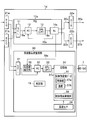
- FIG. 1 is a configuration diagram of a clock network in which a clock frequency monitoring device according to a first embodiment of the present invention is used.
- 1 is a configuration diagram of a clock frequency monitoring device according to a first embodiment of the present invention.
- FIG. 3 is a configuration diagram of a loopback oscillator.
- FIG. 7 is a diagram illustrating a time variation of a control value when a clock input to the clock frequency monitoring device is normal.
- FIG. 6 is a diagram illustrating a time variation of a control value when a clock input to the clock frequency monitoring device is abnormal.
- FIG. 6 is a configuration diagram of a clock frequency monitoring device according to a second embodiment of the present invention. It is a flowchart explaining operation
- FIG. 9 is a configuration diagram of a clock frequency monitoring device according to a third embodiment of the present invention. It is a block diagram of the clock frequency monitoring apparatus which is a modification of this invention.
- FIG. 1 is a configuration diagram of a clock network in which a clock frequency monitoring device according to a first embodiment of the present invention is used.
- Ethernet registered trademark
- the master clock supply device 3 and the plurality of clock supply devices 4a, 4b, 5a, 5b, 5c, 5d, 1a, 1b, 1c, 1d, 1e, 1f, 1g, 1h as frequency monitoring devices are It employs synchronous Ethernet (SyncE) technology.
- each clock supply device reproduces the clock signal (analog signal) of the transmission device by extracting the clock timing (rising timing of the bit string) of the Ethernet signal transmitted from the upstream side. Then, the clock supply device performs frequency conversion to the Gb Ethernet signal speed and transmits the clock signal to the downstream side. Thereby, the clock network 100 transmits the clock in a pyramid shape from the upstream side to the downstream side via the physical layer.
- the clock network 100 includes a master clock supply device 3, a plurality of clock supply devices 4a, 4b, 5a, 5b, 5c, 5d, 1a, 1b, 1c, 1d, 1e, 1f, 1g, and 1h.
- the master clock supply device 3 generates a master clock.
- the clock supply devices 4a and 4b are provided, for example, in a relay building between prefectures, and generate clocks synchronized with a master clock.
- the clock supply devices 5a, 5b, 5c, 5d are arranged, for example, in a relay building in the prefecture.
- the clock supply devices 5a and 5b generate clocks synchronized with the clock supply device 4a.
- the clock supply devices 5c and 5d generate clocks synchronized with the clock supply device 4b.
- the clock supply devices 5c and 5d adopt a redundant configuration.
- a clock synchronized with the clock supply device 4b cannot be generated, a clock synchronized with the clock supply device 4a is preliminary generated.
- a path in which the lower clock supply devices 5a and 5b receive the clock generated by the upper clock supply device 4a in a normal state is referred to as a selection (or N (Normal)) clock path.
- a path through which the lower clock supply devices 5c and 5d receive the clock generated by the upper clock supply device 4a when an abnormality occurs is referred to as a standby (or E (Emergency) system) clock path.
- the clock supply devices 1a, 1b, 1c, 1d, 1e, 1f, 1g, 1h are arranged, for example, in a terminal building.
- the clock supply devices 1a and 1b generate clocks synchronized with the clock supply device 5a.
- the clock supply devices 1c and 1d generate clocks synchronized with the clock supply device 5b.
- the clock supply devices 1e and 1f generate clocks synchronized with the clock supply device 5c.
- the clock supply devices 1g and 1h generate clocks synchronized with the clock supply device 5d.
- the clock supply devices 1c and 1d when the clock supply devices 1c and 1d cannot generate a clock synchronized with the clock supply device 5b, the clock supply devices 1c and 1d preliminary generate a clock synchronized with the clock supply device 5a.
- the clock supply devices 1g and 1h cannot generate a clock synchronized with the clock supply device 5d, the clock supply devices 1g and 1h preliminary generate a clock synchronized with the clock supply device 5c.
- a plurality of clock supply devices 1a, 1b, 1c, 1d, 1e, 1f, 1g, 1h arranged in a terminal building are provided with a GPS (Global Positioning System) or a GPS (Global Positioning System) for monitoring the frequency accuracy of the clock.
- the cesium oscillator 6 may be connected.
- the clock supply target devices 2a, 2b, 2c, 2e, 2f, 2g, 2h are transmission devices, dedicated service nodes, and the like.
- FIG. 2 is a configuration diagram of the clock frequency monitoring device according to the first embodiment of the present invention.
- a clock supply device 1a as a clock frequency monitoring device includes a plurality of frequency receiving units (REC (Receiver)) 21a and 21b, a PLL (Phase Looked Loop) oscillation circuit 10a, a determination unit 19, and a plurality of frequency distribution units (RECs).
- DIS Distribution
- the frequency receiving units 21a and 21b receive a clock via the physical layer. Note that the frequency receiving unit 21a receives the clock of the selected clock path, and the frequency receiving unit 21b receives the clock of the standby clock path.
- the frequency distribution units 22a and 22b distribute the reproduced clocks 20a and 20b reproduced by the PLL oscillation circuit 10a to the clock supply target devices 2a, 2b, 2c, 2e, 2f, 2g, and 2h (FIG. 1).
- the PLL oscillation circuit 10a generates a synchronous clock 18e and reproduced clocks 20a and 20b that are phase-synchronized with one of the selected system clock path and the standby system clock path.
- the PLL oscillation circuit 10a includes a selector (SEL) 11, a phase difference detector (PC (Phase Comparator)) 12 as a phase comparator, a CPU (Central Processing Unit) 13, and a loopback oscillator (Rb) 14a. It is configured with.
- the selector 11 switches between the selected system clock path and the standby system clock path, and outputs one of the clocks to the phase difference detection unit 12.
- the phase difference detector 12 is a phase comparator that outputs a phase comparison signal 18b indicating the phase difference between the input clock 18a selected by the selector 11 and the feedback clock (synchronous clock 18e) generated by the loopback oscillator 14a.
- the CPU 13 performs low-pass filtering (LPF (Low Pass Filter)) on the phase comparison signal 18b. By this calculation, the CPU 13 outputs a voltage value (control value 18c) that specifies the frequency of the clock (the synchronous clock 18e and the reproduced clocks 20a and 20b) generated by the loopback oscillator 14a.
- the determination unit 19 observes the amount of change in the control value 18c as an output signal, and determines whether the frequency is normal / abnormal based on whether the amount of change is large or small.
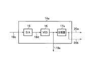
- FIG. 3 is a configuration diagram of the loopback oscillator.
- the loopback oscillator 14a includes a D / A converter 15, a voltage controlled oscillator 16, and a frequency divider 17a.
- the D / A converter 15 converts a digital signal of the control value 18c output from the CPU 13 into an analog signal.
- the voltage controlled oscillator 16 generates a clock (synchronous clock 18e) having a frequency corresponding to the analog signal of the control value 18c.
- the voltage controlled oscillator 16 is configured by adding, for example, a variable capacitance diode to an LC resonance circuit or crystal.
- the loopback oscillator 14a may be a rubidium oscillator whose frequency can be changed using a digital signal.
- the PLL oscillation circuit 10a performs feedback control so that the frequency of the input clock 18a matches the frequency of the synchronous clock 18e generated by the voltage controlled oscillator 16.
- the phase difference detector 12 outputs the phase comparison signal 18b having a predetermined steady phase difference. For example, when the frequency of the input clock 18a that is the selection system clock or the standby system clock is 6.312 MHz, the frequency of the synchronization clock 18e becomes 6.312 MHz, and the frequency of the divided reproduction clocks 20a and 20b becomes 64 kHz. Become.
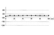
- FIG. 4 is a diagram showing the time variation of the control value when the clock input to the clock frequency monitoring device is normal.
- FIG. 5 is a diagram showing the control value when the clock input to the clock frequency monitoring device is abnormal. It is a figure showing a time change.
- the vertical axis indicates the control value (digital value) 18c of -1200 to 1300, and the horizontal axis indicates the time of 0 to 100 [sec].
- the determination unit 19 of the clock supply device 1a observes the amount of fluctuation (fluctuation width) of the control value 18c, thereby monitoring the normal / abnormal of the input clock 18a (selection clock or standby clock). It has a function as a frequency monitoring device.
- the normality / abnormality of the selected system clock is determined by observing the control value 18c at the time of reproducing the selected system clock.
- the synchronous clock 18e of the selected system clock and the backup system clock are determined.
- LPF low-pass filtering
- FIG. 6 is a configuration diagram of a clock frequency monitoring device according to a second embodiment of the present invention.
- the clock supply device 1b as a clock frequency monitoring device includes a plurality of frequency receiving units 21a and 21b, a PLL oscillation circuit 10a, and a plurality of frequency distribution units 22a and 22b described in the first embodiment.
- the monitoring unit 30 is provided.
- the frequency monitoring unit 30 includes a selector (SEL) 31, a phase difference detection unit (PC) 32, a CPU 33, a storage unit 34, a phase difference correction unit 35, a temperature sensor 36, and a determination unit 19, It is communicably connected to an external network operation system (NE-OpS) 7.
- SEL selector
- PC phase difference detection unit
- NE-OpS external network operation system
- the selector 31 outputs the clock of the standby clock path to the phase difference correction unit 35 when the selector 11 selects the selected clock path, and outputs the clock of the selected clock path when the selector 11 selects the standby clock path. Is output to the phase difference correction unit 35. That is, the selector 31 outputs exclusively to the selector 11.
- the phase difference correction unit 35 corrects the phase difference between one of the selected system clock path and the standby system clock path selected by the selector 31 and outputs the phase-corrected clock to the phase difference detection unit 32.
- the correction amount of the phase difference correction unit 35 is, for example, a normal phase difference between the clock of the selected system clock path and the clock of the standby system clock path.
- the phase difference detector 32 outputs a phase difference between the output clock of the phase difference corrector 35 and the synchronous clock 18e output from the voltage controlled oscillator 16 (FIG. 3) of the loopback oscillator 14a.
- the CPU 33 performs low-pass filtering (LPF) on the phase difference output from the phase difference detection unit 32, and outputs a control value 37a.
- the storage unit 34 stores control value fluctuation data 37 and a control value abnormality threshold 38.
- the control value fluctuation data 37 is time-series data of a combination of the control value 37a and the temperature 37b.
- the temperature sensor 36 detects a temperature 37 b that is a cause of noise (jitter, wander) fluctuation, and stores the temperature 37 b in the storage unit 34.
- the determination unit 19 regards the frequency as abnormal when the difference between the control value 37a and the control value abnormality threshold 38 is equal to or greater than a predetermined amount.
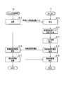
- FIG. 7 is a flowchart illustrating the operation of the clock frequency monitoring device according to the second embodiment of the present invention.
- the clock supply device 1b as the clock frequency monitoring device transmits a control ID specifying itself, control value fluctuation data 37, and a control value abnormality threshold 38 to the network operation system 7 (S11).
- the network operation system 7 receives these data (S12), classifies the control value 37a of the control value fluctuation data 37 by the temperature 37b, and determines the distribution width of the control value 37a for each temperature 37b (S13).
- the network operation system 7 regards the distribution width of the determined control value 37a as the influence of noise, and specifies a control value from which the influence of noise has been removed for each temperature 37b (S14).
- the network operation system 7 transmits the upper limit value and the lower limit value of the control value 37a from which the influence of the noise has been removed to the clock supply device 1b as the control value abnormality threshold 38 (S15).
- the clock supply device 1b updates the control value abnormality threshold 38 in the storage unit 34 (S16). Then, when the sequentially measured control value 37a deviates from the control value abnormality threshold 38, the clock supply device 1b regards the clock frequency as abnormal and transmits an alarm to the network operation system 7 (S17).
- the network operation system 7 receives the alarm (S18) and notifies the worker.
- the control value 37a calculated by the frequency monitoring unit 30 is such that the phase difference between the selected system clock reproduced by the PLL oscillation circuit 10a and the backup system clock is set to a low band. It is a result of filtering (LPF) operation.
- the control value 18c obtained by performing low-pass filtering on the phase difference corresponds to the frequency.
- the control value 37a obtained by calculating the phase difference by low-pass filtering (LPF) also corresponds to the frequency. That is, the determination unit 19 can determine the frequency abnormality based on the behavior of the control value 37a.
- the frequency of a standby clock is monitored using a GPS or a cesium oscillator 6.
- the clock supply device 1h (FIG. 1) includes a GPS and a cesium oscillator 6. According to this, the frequency quality management unit that monitors the frequency needs a GPS signal for reference and an expensive cesium oscillator 6 with high frequency stability.
- the determination unit 19 of the clock supply device 1a according to the first embodiment determines whether the frequency is normal or abnormal based on the magnitude of the variation of the control value 18c.
- the determination unit 19 of the clock supply device 1b according to the second embodiment determines that the frequency is abnormal when the difference between the control value 37a and the control value abnormality threshold 38 exceeds a predetermined amount. Therefore, the clock supply devices 1a and 1b of the first and second embodiments do not require the GPS or the cesium oscillator 6 for monitoring the frequency, so that the cost is low.
- the clock supply devices 1a and 1b feed back the synchronous clock 18e generated by the loop-back oscillator 14a to the phase difference detecting unit 12, it is also possible to divide the frequency of the synchronous clock 18e and then feed it back to the phase difference detecting unit 12. .
- FIG. 8 is a configuration diagram of a clock frequency monitoring device according to a third embodiment of the present invention.
- a clock supply device 1c as a clock frequency monitoring device includes a plurality of frequency reception units 21a and 21b and a PLL oscillation circuit 10b, similarly to the clock supply devices 1a (FIG. 2) and 1b (FIG. 6) of the first embodiment. And a plurality of frequency distribution units 22a and 22b.
- the PLL oscillation circuit 10b includes a selector 11, a phase difference detection unit 12, a CPU (Central Processing Unit) 13, a loopback oscillator 14b, and a frequency divider 17b. Further, the loopback oscillator 14b does not have the frequency divider 17a (FIG. 3), and outputs the synchronous clock 18e generated by the voltage controlled oscillator 16 (FIG. 3) as reproduced clocks 20a and 20b.
- the frequency divider 17b divides the frequency of the synchronous clock 18e generated by the loopback oscillator 14b into 1 / N, and inputs the frequency-divided clock 18f to the phase difference detector 12. That is, the phase difference detection unit 12 outputs the phase difference between the input clock 18a and the frequency-divided clock 18f to the CPU 13.
- the CPU 13 outputs a control value 18c for voltage-controlling the oscillation frequency of the loopback oscillator 14b by performing a low-pass filtering operation (LPF).
- LPF low-pass filtering operation
- the loop-back oscillator 14b generates the synchronous clock 18e and the reproduced clocks 20a, 20b having a frequency N times the frequency of the input clock 18a.
- N 99
- the frequency of the reproduced clocks 20a and 20b is 6.312 MHz.
- the present invention is not limited to the above-described embodiment.
- the phase difference detector 32 (FIG. 6) of the second embodiment outputs the phase difference between the synchronous clock 18e and the output clock of the phase difference corrector 35.
- a clock in which the phase of the synchronous clock 18e is corrected using the phase difference correction unit 35, and a clock in which the phase of the synchronous clock 18e is corrected using the phase difference detection unit 12, A phase difference from the input clock of the backup path may be generated.
Landscapes
- Physics & Mathematics (AREA)
- Engineering & Computer Science (AREA)
- Nonlinear Science (AREA)
- General Engineering & Computer Science (AREA)
- General Physics & Mathematics (AREA)
- Theoretical Computer Science (AREA)
- Computer Networks & Wireless Communication (AREA)
- Signal Processing (AREA)
- Stabilization Of Oscillater, Synchronisation, Frequency Synthesizers (AREA)
- Synchronisation In Digital Transmission Systems (AREA)
Abstract
【課題】入力クロックと該入力クロックに同期した同期クロックとの周波数差を監視する。 【解決手段】入力クロック18aの周波数を監視するクロック周波数監視装置であって、入力クロック18aに位相同期した同期クロック18e又は該同期クロック18eを分周した第1分周クロック18fの位相と入力クロック18aの位相とを比較する位相比較器12と、位相比較器12の出力信号を低域濾波するフィルタ13と、フィルタ13の制御値に対応する周波数の同期クロック18eを生成する発振器14と、フィルタ13の出力信号の変動幅が所定範囲以上になったときに入力クロック18aの周波数異常と判定する判定部19とを備える。
Description
本発明は、クロック周波数監視装置、及びクロック周波数監視方法に関する。
現在、電話や専用線といった通信サービスの多くは、デジタル伝送方式を用いている。このデジタル伝送方式において、多重分離、クロスコネクトするにはネットワーク内の各装置の動作クロックを一致させる網同期をする必要がある。我が国では、網同期を実現するため、主局のクロック周波数に従属局のクロック周波数を合わせる従属同期方式を用いており、クロック網は標準クロック発生装置を頂点とした階層的な網構成となっている(図1)。
特許文献1には、ネットワーク内で接続される装置間で周波数同期を行う場合、上流側の装置は下流側の装置に周波数同期の品質状態を示す情報を送信する技術が開示されている。
ところで、ネットワーク内で周波数同期を行う場合、信頼性向上のため、上位の装置からクロックを受信する受信部の冗長化が図られている。つまり、複数の上流側装置何れかから配信されるクロックに同期した同期クロック(選択系クロック)を配信できないときには、他の上流側装置から配信されるクロック(予備系クロック)に同期した同期クロックを配信するように構成されている。
ところが、特許文献1に開示されている技術では、クロック精度の確認を行う手段を有していない。特に、特許文献1に開示されている技術を用いて、選択系クロックの配信を行っている場合に、予備系クロックの精度を確認するときには、GPS(Global Positioning System)やセシウム発振器等のレファレンス情報が必要になってしまう。
本発明は、このような問題点を解決するためになされたものであり、入力クロックと該入力クロックに同期した同期クロックとの周波数差を監視することができるクロック周波数監視装置、及び周波数監視方法を提供することを目的とする。
請求項1に係る発明は、第1入力クロック(例えば、選択系クロック)に同期した同期クロックを再生すると共に、該第1入力クロックに周波数同期すべき第2入力クロック(例えば、予備系クロック)の周波数を監視するクロック周波数監視装置であって、前記同期クロック又は該同期クロックを分周した第1分周クロックの位相と前記第1入力クロックの位相とを比較する第1位相比較器(12)と、前記第1位相比較器の出力信号を低域濾波する第1フィルタ(CPU13)と、前記第1フィルタの出力信号(例えば、制御値)に対応する周波数の前記同期クロックを生成する発振器(14)と、前記同期クロック又は前記第1分周クロックの位相と前記第2入力クロックの位相とを比較する第2位相比較器(32)と、前記第2位相比較器の出力信号を低域濾波する第2フィルタ(CPU33)と、前記第2フィルタの出力信号の変動幅が所定範囲以上になったときに、前記第2入力クロックの周波数異常と判定する判定部(7)と、を備えることを特徴とする。なお、括弧内の符号や文字は、実施形態において付した符号等であって、本発明を限定するものではない。
請求項1に係る発明によれば、第1入力クロックに位相同期した同期クロックが生成される。第2入力クロックと同期クロック又は該同期クロックを分周した第1分周クロックの位相との位相ロックが外れたら、第2フィルタの出力信号の変動幅が大きくなる。このため、第2フィルタの出力信号の変動幅を監視することにより、第2入力クロックの周波数異常を判定することができる。
請求項2に係る発明は、請求項1に記載のクロック周波数監視装置であって、前記所定範囲は、自装置の温度によって変化させられることを特徴とする。これによれば、温度により変化するノイズを考慮して、異常判定することができる。
請求項3に係る発明は、入力クロック(18a、選択系クロック又は予備系クロック)の周波数を監視するクロック周波数監視装置であって、前記入力クロックに位相同期した同期クロック(18e)又は該同期クロックを分周した第1分周クロック(18f)の位相と前記入力クロックの位相とを比較する位相比較器(12)と、前記位相比較器の出力信号を低域濾波するフィルタ(CPU13)と、前記フィルタの出力信号(例えば、制御値)に対応する周波数の前記同期クロックを生成する発振器(14)と、前記フィルタの出力信号の変動幅が所定範囲以上になったときに前記入力クロックの周波数異常と判定する判定部(19)と、を備えることを特徴とする。
請求項3に係る発明では、入力クロックと同期クロックとの位相ロックが外れたら、フィルタの出力信号の変動幅が大きくなる。このため、フィルタの出力信号の変動幅を監視することにより、入力クロックの周波数異常を判定することができる。
請求項4に係る発明は、請求項1乃至請求項3の何れか一項に記載のクロック周波数監視装置であって、前記同期クロック又は該同期クロックを分周した分周クロック(20a,20b)を配信する配信部(22a,22b)をさらに備えることを特徴とする。これによれば、同期信号又は該同期信号を分周した分周信号が下流側に配信される。
請求項5に係る発明は、第1入力クロックに同期した同期クロックを再生すると共に、該第1入力クロックに周波数同期すべき第2入力クロックの周波数を監視するクロック周波数監視装置が実行するクロック周波数監視方法であって、前記同期クロック又は該同期クロックを分周した第1分周クロックの位相と前記第1入力クロックの位相とを比較する第1位相比較ステップと、前記第1位相比較ステップの出力信号を低域濾波する第1フィルタステップと、前記第1フィルタステップで演算した第1濾波信号に対応する周波数の前記同期クロックを発振器に生成させる発振ステップと、前記同期クロック又は前記第1分周クロックの位相と前記第2入力クロックの位相とを比較する第2位相比較ステップと、前記第2位相比較ステップの出力信号を低域濾波演算する第2フィルタステップと、前記第2フィルタステップで演算した第2低域濾波信号の変動幅が所定範囲以上になったときに、前記第2入力クロックの周波数異常と判定する判定ステップと、を備えることを特徴とする。
請求項5に係る発明によれば、第1入力クロックに位相同期した同期クロックが生成される。第2入力クロックと同期クロック又は該同期クロックを分周した第1分周クロックの位相との位相ロックが外れたら、第2フィルタステップで演算した第2低域濾波信号の変動幅が大きくなる。このため、第2低域濾波信号の変動幅を監視することにより、第2入力クロックの周波数異常を判定することができる。
請求項6に係る発明は、入力クロックの周波数を監視するクロック周波数監視装置が実行するクロック周波数監視方法であって、前記入力クロックに位相同期した同期クロック又は該同期クロックを分周した第1分周クロックの位相と前記入力クロックの位相とを比較する位相比較ステップと、前記位相比較ステップの出力信号を低域濾波するフィルタステップと、前記フィルタステップで演算した低域濾波信号に対応する周波数の前記同期クロックを発振器に生成させる発振ステップと、前記低域濾波信号の変動幅が所定範囲以上になったときに前記入力クロックの周波数異常と判定する判定ステップと、を備えることを特徴とする。
このため、フィルタの出力信号の変動幅を監視することにより、入力クロックの周波数異常を判定することができる。
本発明によれば、入力クロックと該入力クロックに同期した同期クロックとの周波数差を監視することができる。
以下、図面を参照して、本発明の実施の形態(以下、「本実施形態」と称する)につき詳細に説明する。なお、各図は、本発明を十分に理解できる程度に、概略的に示してあるに過ぎない。また、各図において、共通する構成要素や同様な構成要素については、同一の符号を付し、それらの重複する説明を省略する。
(第1実施形態)
図1は、本発明の第1実施形態であるクロック周波数監視装置が使用されるクロック網の構成図である。
イーサネット(登録商標)は非同期方式であるので、送信側と受信側で周波数偏差が発生する。イーサネット上でクロックを伝送するためには,各装置内部の発振周波数をクロック信号に同期させる必要がある。このため、マスタクロック供給装置3と、周波数監視装置としての複数のクロック供給装置4a,4b,5a,5b,5c,5d,1a,1b,1c,1d,1e,1f,1g,1hとは、シンクロナスイーサネット(SyncE)技術を採用している。
図1は、本発明の第1実施形態であるクロック周波数監視装置が使用されるクロック網の構成図である。
イーサネット(登録商標)は非同期方式であるので、送信側と受信側で周波数偏差が発生する。イーサネット上でクロックを伝送するためには,各装置内部の発振周波数をクロック信号に同期させる必要がある。このため、マスタクロック供給装置3と、周波数監視装置としての複数のクロック供給装置4a,4b,5a,5b,5c,5d,1a,1b,1c,1d,1e,1f,1g,1hとは、シンクロナスイーサネット(SyncE)技術を採用している。
つまり、クロック網100では、各々のクロック供給装置は、上流側から伝送されたイーサネット信号のクロックタイミング(ビット列の立ち上がりタイミング)を抽出することで、送信装置のクロック信号(アナログ信号)を再生する。そして、該クロック供給装置は、Gbイーサネットの信号速度に周波数変換を行い、クロック信号を下流側に送信している。これにより、クロック網100は、クロックを物理層を介して上流側から下流側までピラミッド状に伝送している。
クロック網100は、マスタクロック供給装置3と、複数のクロック供給装置4a,4b,5a,5b,5c,5d,1a,1b,1c,1d,1e,1f,1g,1hと、末端のクロック供給装置1a,1b,1c,1d,1e,1f,1g,1hに接続されているクロック供給対象装置2a,2b,・・・,2e,2f,2g,2hと、何れか1又は複数のクロック供給対象装置1hが備えるセシウム発振器6とを備えて構成される。
マスタクロック供給装置3は、マスタクロックを生成する。クロック供給装置4a,4bは、例えば、県間の中継ビルに配設されており、マスタクロックに同期したクロックを生成する。クロック供給装置5a,5b,5c,5dは、例えば、県内の中継ビルに配設されている。クロック供給装置5a,5bは、クロック供給装置4aに同期したクロックを生成する。クロック供給装置5c,5dは、クロック供給装置4bに同期したクロックを生成する。
また、クロック供給装置5c,5dは、冗長構成を採用しており、クロック供給装置4bに同期したクロックを生成することができないときに、予備的に、クロック供給装置4aに同期したクロックを生成する。ここで、正常時に、上位のクロック供給装置4aが生成するクロックを下位のクロック供給装置5a,5bが受信する経路を選択系(又は、N(Normal)系)クロックパスという。また、異常時に、上位のクロック供給装置4aが生成するクロックを下位のクロック供給装置5c,5dが受信する経路を予備系(又は、E(Emergency)系)クロックパスという。
クロック供給装置1a,1b,1c,1d,1e,1f,1g,1hは、例えば、末端のビルに配設されている。クロック供給装置1a,1bは、クロック供給装置5aに同期したクロックを生成する。クロック供給装置1c,1dは、クロック供給装置5bに同期したクロックを生成する。クロック供給装置1e,1fは、クロック供給装置5cに同期したクロックを生成する。クロック供給装置1g,1hは、クロック供給装置5dに同期したクロックを生成する。
例えば、クロック供給装置1c,1dは、クロック供給装置5bに同期したクロックを生成することができないときに、予備的に、クロック供給装置5aに同期したクロックを生成する。また、クロック供給装置1g,1hは、クロック供給装置5dに同期したクロックを生成することができないときに、予備的に、クロック供給装置5cに同期したクロックを生成する。
また、末端ビルに配設されている複数のクロック供給装置1a,1b,1c,1d,1e,1f,1g,1hは、クロックの周波数精度を監視するために、GPS(Global Positioning System)や、セシウム発振器6を接続することがある。
クロック供給対象装置2a,2b,2c,2e,2f,2g,2hは、伝送装置や、専用サービスノード等であり、例えば、図1に示す一つのクロック供給装置1gから複数のクロック供給対象装置2g,2hに接続されることがある。
図2は、本発明の第1実施形態であるクロック周波数監視装置の構成図である。
クロック周波数監視装置としてのクロック供給装置1aは、複数の周波数受信部(REC(Receiver))21a,21bと、PLL(Phase Looked Loop)発振回路10aと、判定部19と、複数の周波数配信部(DIS(Distribution))22a,22bとを備えて構成される。周波数受信部21a,21bは、物理層を介してクロックを受信する。なお、周波数受信部21aは、選択系クロックパスのクロックを受信し、周波数受信部21bは、予備系クロックパスのクロックを受信する。周波数配信部22a,22bは、PLL発振回路10aが再生した再生クロック20a,20bをクロック供給対象装置2a,2b,2c,2e,2f,2g,2h(図1)に分配する。
クロック周波数監視装置としてのクロック供給装置1aは、複数の周波数受信部(REC(Receiver))21a,21bと、PLL(Phase Looked Loop)発振回路10aと、判定部19と、複数の周波数配信部(DIS(Distribution))22a,22bとを備えて構成される。周波数受信部21a,21bは、物理層を介してクロックを受信する。なお、周波数受信部21aは、選択系クロックパスのクロックを受信し、周波数受信部21bは、予備系クロックパスのクロックを受信する。周波数配信部22a,22bは、PLL発振回路10aが再生した再生クロック20a,20bをクロック供給対象装置2a,2b,2c,2e,2f,2g,2h(図1)に分配する。
PLL発振回路10aは、選択系クロックパスと予備系クロックパスとの何れか一方のクロックに位相同期した同期クロック18e及び再生クロック20a,20bを生成する。PLL発振回路10aは、セレクタ(SEL)11と、位相比較器としての位相差検出部(PC(Phase Comparator))12と、CPU(Central Processing Unit)13と、ループバック発振器(Rb)14aとを備えて構成される。
セレクタ11は、選択系クロックパスと予備系クロックパスとを切り替えて、何れか一方のクロックを位相差検出部12に出力する。位相差検出部12は、セレクタ11が選択した入力クロック18aと、ループバック発振器14aが生成した帰還クロック(同期クロック18e)との位相差を示す位相比較信号18bを出力する位相比較器である。CPU13は、位相比較信号18bを低域濾波(LPF(Low Pass Filter))演算する。この演算により、CPU13は、ループバック発振器14aが生成するクロック(同期クロック18e,再生クロック20a,20b)の周波数を特定する電圧値(制御値18c)を出力する。判定部19は、出力信号としての制御値18cの変動量を観測し、変動量の大/小により、周波数の正常/異常を判定する。
図3は、ループバック発振器の構成図である。
ループバック発振器14aは、D/A変換器15と、電圧制御発振器16と、分周器17aとを備えて構成される。
D/A変換器15は、CPU13が出力する制御値18cのデジタル信号をアナログ信号に変換する。電圧制御発振器16は、制御値18cのアナログ信号に対応する周波数のクロック(同期クロック18e)を生成する。なお、電圧制御発振器16は、LC共振回路や水晶に、例えば、可変容量ダイオードを付加して構成される。分周器17aは、同期クロック18eを(1/N(例えば、N=99))に分周して、再生クロック20a,20bを生成する。なお、ループバック発振器14aは、デジタル信号を用いて、周波数可変可能なルビジウム発振器であっても構わない。
ループバック発振器14aは、D/A変換器15と、電圧制御発振器16と、分周器17aとを備えて構成される。
D/A変換器15は、CPU13が出力する制御値18cのデジタル信号をアナログ信号に変換する。電圧制御発振器16は、制御値18cのアナログ信号に対応する周波数のクロック(同期クロック18e)を生成する。なお、電圧制御発振器16は、LC共振回路や水晶に、例えば、可変容量ダイオードを付加して構成される。分周器17aは、同期クロック18eを(1/N(例えば、N=99))に分周して、再生クロック20a,20bを生成する。なお、ループバック発振器14aは、デジタル信号を用いて、周波数可変可能なルビジウム発振器であっても構わない。
PLL発振回路10aは、入力クロック18aの周波数と電圧制御発振器16が生成する同期クロック18eの周波数とが一致するように、帰還制御する。これにより、位相差検出部12は、所定の定常位相差を有する位相比較信号18bを出力する。例えば、選択系クロック又は予備系クロックである入力クロック18aの周波数が6.312MHzのとき、同期クロック18eの周波数は、6.312MHzになり、分周後の再生クロック20a,20bの周波数が64kHzとなる。
図4は、クロック周波数監視装置に入力されるクロックが正常なときの制御値の時間変動を示す図であり、図5は、クロック周波数監視装置に入力されるクロックが異常なときの制御値の時間変動を示す図である。縦軸は、-1200~1300の制御値(デジタル値)18cを示し、横軸は、0~100[sec]の時間を示している。
図4では、入力クロック(選択系クロック又は予備系クロック)が正常なので、入力クロック18aと同期クロック18eとの周波数偏差が無く、制御値18cが一定値を示している。一方、図5では、入力クロックの周波数に異常が発生し、入力クロック18aと同期クロック18eとの周波数偏差が発生し、制御値18cの変動が生じている。特に、60~80[sec]において、制御値18cは大きな変動量を示し、入力クロック18aが異常な状態を示していると推認される。このように、クロック供給装置1aの判定部19は、制御値18cの変動量(変動幅)を観測することにより、入力クロック18a(選択系クロック又は予備系クロック)の正常/異常を監視するクロック周波数監視装置としての機能を有する。
(第2実施形態)
前記第1実施形態では、選択系クロックを再生させるときの制御値18cを観測することにより、選択系クロックの正常/異常を判定したが、選択系クロックの同期クロック18eと、予備系クロックとの位相差を低域濾波(LPF)演算した制御値18cの推移を観測することにより、予備系クロックの正常/異常を判定することができる。
前記第1実施形態では、選択系クロックを再生させるときの制御値18cを観測することにより、選択系クロックの正常/異常を判定したが、選択系クロックの同期クロック18eと、予備系クロックとの位相差を低域濾波(LPF)演算した制御値18cの推移を観測することにより、予備系クロックの正常/異常を判定することができる。
図6は、本発明の第2実施形態であるクロック周波数監視装置の構成図である。
クロック周波数監視装置としてのクロック供給装置1bは、前記第1実施形態で説明した複数の周波数受信部21a,21bと、PLL発振回路10aと、複数の周波数配信部22a,22bとに加えて、周波数監視部30を備えている。
クロック周波数監視装置としてのクロック供給装置1bは、前記第1実施形態で説明した複数の周波数受信部21a,21bと、PLL発振回路10aと、複数の周波数配信部22a,22bとに加えて、周波数監視部30を備えている。
周波数監視部30は、セレクタ(SEL)31と、位相差検出部(PC)32と、CPU33と、記憶部34と、位相差補正部35と、温度センサ36と、判定部19とを備え、外部のネットワークオペレーションシステム(NE-OpS)7に通信可能に接続される。
セレクタ31は、セレクタ11が選択系クロックパスを選択したときに、予備系クロックパスのクロックを位相差補正部35に出力し、セレクタ11が予備系クロックパスを選択したときに、選択系クロックパスのクロックを位相差補正部35に出力する。つまり、セレクタ31は、セレクタ11と排他的に出力する。
位相差補正部35は、セレクタ31が選択した選択系クロックパス及び予備系クロックパスの何れか一方のクロックの位相差を補正し、位相補正したクロックを位相差検出部32に出力する。位相差補正部35の補正量は、例えば、選択系クロックパスのクロックと、予備系クロックパスのクロックとの正常時の位相差である。
位相差検出部32は、位相差補正部35の出力クロックと、ループバック発振器14aの電圧制御発振器16(図3)が出力する同期クロック18eとの位相差を出力する。CPU33は、位相差検出部32が出力した位相差を低域濾波(LPF)演算し、制御値37aを出力する。記憶部34は、制御値変動データ37と、制御値異常閾値38とを格納する。制御値変動データ37は、制御値37a及び温度37bの組合せの時系列データである。温度センサ36は、ノイズ(ジッタ、ワンダ)の変動要因である温度37bを検出し、記憶部34に記憶する。
判定部19は、制御値37aと、制御値異常閾値38との差異が所定量以上になったときに、周波数異常とみなす。
図7は、本発明の第2実施形態であるクロック周波数監視装置の動作を説明するフローチャートである。
クロック周波数監視装置としてのクロック供給装置1bは、自身を特定する制御ID、制御値変動データ37と、制御値異常閾値38とをネットワークオペレーションシステム7に送信する(S11)。ネットワークオペレーションシステム7は、これらのデータを受信し(S12)、制御値変動データ37の制御値37aを温度37bで分類して、制御値37aの分布幅を温度37b毎に決定する(S13)。ネットワークオペレーションシステム7は、決定された制御値37aの分布幅をノイズの影響と見なし、ノイズの影響を除去した制御値を温度37b毎に特定する(S14)。ネットワークオペレーションシステム7は、このノイズの影響を除去した制御値37aの上限値及び下限値を制御値異常閾値38としてクロック供給装置1bに送信する(S15)。クロック供給装置1bは、記憶部34の制御値異常閾値38を更新する(S16)。そして、クロック供給装置1bは、逐次測定した制御値37aが制御値異常閾値38から外れたら、クロック周波数の異常とみなし、警報をネットワークオペレーションシステム7に送信する(S17)。ネットワークオペレーションシステム7は、警報を受信し(S18)、作業者に報知する。
クロック周波数監視装置としてのクロック供給装置1bは、自身を特定する制御ID、制御値変動データ37と、制御値異常閾値38とをネットワークオペレーションシステム7に送信する(S11)。ネットワークオペレーションシステム7は、これらのデータを受信し(S12)、制御値変動データ37の制御値37aを温度37bで分類して、制御値37aの分布幅を温度37b毎に決定する(S13)。ネットワークオペレーションシステム7は、決定された制御値37aの分布幅をノイズの影響と見なし、ノイズの影響を除去した制御値を温度37b毎に特定する(S14)。ネットワークオペレーションシステム7は、このノイズの影響を除去した制御値37aの上限値及び下限値を制御値異常閾値38としてクロック供給装置1bに送信する(S15)。クロック供給装置1bは、記憶部34の制御値異常閾値38を更新する(S16)。そして、クロック供給装置1bは、逐次測定した制御値37aが制御値異常閾値38から外れたら、クロック周波数の異常とみなし、警報をネットワークオペレーションシステム7に送信する(S17)。ネットワークオペレーションシステム7は、警報を受信し(S18)、作業者に報知する。
以上説明したように、本実施形態のクロック供給装置1bは、周波数監視部30が演算する制御値37aは、PLL発振回路10aが再生する選択系クロックと、予備系クロックとの位相差を低域濾波(LPF)演算したものである。PLL発振回路10aにおいて、位相差を低域濾波演算した制御値18cは、周波数に対応するものである。周波数監視部30でも同様に、位相差を低域濾波(LPF)演算した制御値37aも周波数に対応したものである。つまり、判定部19は、制御値37aの振る舞いにより、周波数異常を判定することができる。
(比較例)
前記第1,2実施形態のクロック供給装置1a,1bと比較する比較例は、GPSやセシウム発振器6を用いて、予備系クロックの周波数を監視するものである。例えば、クロック供給装置1h(図1)は、GPSやセシウム発振器6を設けている。これによれば、周波数を監視する周波数品質管理部は、リファレンス用のGPS信号や周波数安定度の高い高価なセシウム発振器6が必要になる。
前記第1,2実施形態のクロック供給装置1a,1bと比較する比較例は、GPSやセシウム発振器6を用いて、予備系クロックの周波数を監視するものである。例えば、クロック供給装置1h(図1)は、GPSやセシウム発振器6を設けている。これによれば、周波数を監視する周波数品質管理部は、リファレンス用のGPS信号や周波数安定度の高い高価なセシウム発振器6が必要になる。
この比較例に対して、前記第1実施形態のクロック供給装置1aの判定部19は、制御値18cの変動量の大/小により、周波数の正常/異常を判定した。また、前記第2実施形態のクロック供給装置1bの判定部19は、制御値37aと、制御値異常閾値38との差異が所定量以上になったときに、周波数異常とみなしている。したがって、前記第1,2実施形態のクロック供給装置1a,1bは、周波数監視のためのGPSやセシウム発振器6が不要であるので、コストが安い。
(第3実施形態)
クロック供給装置1a,1bは、ループバック発振器14aが生成した同期クロック18eを位相差検出部12に帰還させたが、同期クロック18eを分周させてから位相差検出部12に帰還させることもできる。
クロック供給装置1a,1bは、ループバック発振器14aが生成した同期クロック18eを位相差検出部12に帰還させたが、同期クロック18eを分周させてから位相差検出部12に帰還させることもできる。
図8は、本発明の第3実施形態であるクロック周波数監視装置の構成図である。
クロック周波数監視装置としてのクロック供給装置1cは、第1実施形態のクロック供給装置1a(図2),1b(図6)と同様に、複数の周波数受信部21a,21bと、PLL発振回路10bと、複数の周波数配信部22a,22bとを備えて構成される。PLL発振回路10bは、PLL発振回路10bは、セレクタ11と、位相差検出部12と、CPU(Central Processing Unit)13と、ループバック発振器14bと、分周器17bとを備えて構成される。また、ループバック発振器14bは、分周器17a(図3)を有しておらず、電圧制御発振器16(図3)が生成した同期クロック18eを再生クロック20a,20bとして出力する。
クロック周波数監視装置としてのクロック供給装置1cは、第1実施形態のクロック供給装置1a(図2),1b(図6)と同様に、複数の周波数受信部21a,21bと、PLL発振回路10bと、複数の周波数配信部22a,22bとを備えて構成される。PLL発振回路10bは、PLL発振回路10bは、セレクタ11と、位相差検出部12と、CPU(Central Processing Unit)13と、ループバック発振器14bと、分周器17bとを備えて構成される。また、ループバック発振器14bは、分周器17a(図3)を有しておらず、電圧制御発振器16(図3)が生成した同期クロック18eを再生クロック20a,20bとして出力する。
分周器17bは、ループバック発振器14bが生成する同期クロック18eを1/Nに分周して、分周クロック18fを位相差検出部12に入力する。つまり、位相差検出部12は、入力クロック18aと分周クロック18fとの位相差をCPU13に出力する。CPU13は、低域濾波演算(LPF)することにより、ループバック発振器14bの発振周波数を電圧制御する制御値18cを出力する。
これにより、ループバック発振器14bは、入力クロック18aのN倍の周波数の同期クロック18e及び再生クロック20a,20bを生成する。例えば、N=99の場合、入力クロック18aの周波数が64kHzのとき、再生クロック20a,20bの周波数は、6.312MHzとなる。
(変形例)
本発明は前記した実施形態に限定されるものではなく、例えば、以下のような種々の変形が可能である。
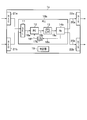
前記第2実施形態の位相差検出部32(図6)では、同期クロック18eと、位相差補正部35の出力クロックとの位相差を出力した。図9に示すように、位相差補正部35を用いて、同期クロック18eの位相を補正したクロックを生成し、位相差検出部12を用いて、該同期クロック18eの位相を補正したクロックと、予備系パスの入力クロックとの位相差を生成しても構わない。
本発明は前記した実施形態に限定されるものではなく、例えば、以下のような種々の変形が可能である。
前記第2実施形態の位相差検出部32(図6)では、同期クロック18eと、位相差補正部35の出力クロックとの位相差を出力した。図9に示すように、位相差補正部35を用いて、同期クロック18eの位相を補正したクロックを生成し、位相差検出部12を用いて、該同期クロック18eの位相を補正したクロックと、予備系パスの入力クロックとの位相差を生成しても構わない。
1,1a,1b,1c,1d,1e,1f,1g,1h クロック供給装置(クロック周波数監視装置)
2a,2b,2c,2h クロック供給対象装置
3 マスタクロック供給装置
4a,4b クロック供給装置(クロック周波数監視装置)
5a,5b,5c,5d クロック供給装置(クロック周波数監視装置)
6 セシウム発振器
7 ネットワークオペレーションシステム
10a,10b PLL発振回路
12 位相差検出部(位相比較器)
13 CPU(低域濾波フィルタ、LPF)
14a,14b ループバック発振器
16 電圧制御発振器
17a,17b 分周器
18a 入力クロック
18b 位相比較信号
18c 制御値(出力信号)
19 判定部
21a,21b 周波数受信部
22a,22b 周波数配信部
30 周波数監視部
33 CPU
37 制御値変動データ
37a 制御値
38 制御値異常閾値
100 クロック網
2a,2b,2c,2h クロック供給対象装置
3 マスタクロック供給装置
4a,4b クロック供給装置(クロック周波数監視装置)
5a,5b,5c,5d クロック供給装置(クロック周波数監視装置)
6 セシウム発振器
7 ネットワークオペレーションシステム
10a,10b PLL発振回路
12 位相差検出部(位相比較器)
13 CPU(低域濾波フィルタ、LPF)
14a,14b ループバック発振器
16 電圧制御発振器
17a,17b 分周器
18a 入力クロック
18b 位相比較信号
18c 制御値(出力信号)
19 判定部
21a,21b 周波数受信部
22a,22b 周波数配信部
30 周波数監視部
33 CPU
37 制御値変動データ
37a 制御値
38 制御値異常閾値
100 クロック網
Claims (6)
- 第1入力クロックに同期した同期クロックを再生すると共に、該第1入力クロックに周波数同期すべき第2入力クロックの周波数を監視するクロック周波数監視装置であって、
前記同期クロック又は該同期クロックを分周した第1分周クロックの位相と前記第1入力クロックの位相とを比較する第1位相比較器と、
前記第1位相比較器の出力信号を低域濾波する第1フィルタと、
前記第1フィルタの出力信号に対応する周波数の前記同期クロックを生成する発振器と、
前記同期クロック又は前記第1分周クロックの位相と前記第2入力クロックの位相とを比較する第2位相比較器と、
前記第2位相比較器の出力信号を低域濾波する第2フィルタと、
前記第2フィルタの出力信号の変動幅が所定範囲以上になったときに、前記第2入力クロックの周波数異常と判定する判定部と、
を備えることを特徴とするクロック周波数監視装置。 - 請求項1に記載のクロック周波数監視装置であって、
前記所定範囲は、自装置の温度によって変化させられる
ことを特徴とするクロック周波数監視装置。 - 入力クロックの周波数を監視するクロック周波数監視装置であって、
前記入力クロックに位相同期した同期クロック又は該同期クロックを分周した第1分周クロックの位相と前記入力クロックの位相とを比較する位相比較器と、
前記位相比較器の出力信号を低域濾波するフィルタと、
前記フィルタの出力信号に対応する周波数の前記同期クロックを生成する発振器と、
前記フィルタの出力信号の変動幅が所定範囲以上になったときに前記入力クロックの周波数異常と判定する判定部と、
を備えることを特徴とするクロック周波数監視装置。 - 請求項1乃至請求項3の何れか一項に記載のクロック周波数監視装置であって、
前記同期クロック又は該同期クロックを分周した第2分周クロックを配信する配信部をさらに備える
ことを特徴とするクロック周波数監視装置。 - 第1入力クロックに同期した同期クロックを再生すると共に、該第1入力クロックに周波数同期すべき第2入力クロックの周波数を監視するクロック周波数監視装置が実行するクロック周波数監視方法であって、
前記同期クロック又は該同期クロックを分周した第1分周クロックの位相と前記第1入力クロックの位相とを比較する第1位相比較ステップと、
前記第1位相比較ステップの出力信号を低域濾波する第1フィルタステップと、
前記第1フィルタステップで演算した第1低域濾波信号に対応する周波数の前記同期クロックを発振器に生成させる発振ステップと、
前記同期クロック又は前記第1分周クロックの位相と前記第2入力クロックの位相とを比較する第2位相比較ステップと、
前記第2位相比較ステップの出力信号を低域濾波演算する第2フィルタステップと、
前記第2フィルタステップで演算した第2低域濾波信号の変動幅が所定範囲以上になったときに、前記第2入力クロックの周波数異常と判定する判定ステップと、
を備えることを特徴とするクロック周波数監視方法。 - 入力クロックの周波数を監視するクロック周波数監視装置が実行するクロック周波数監視方法であって、
前記入力クロックに位相同期した同期クロック又は該同期クロックを分周した第1分周クロックの位相と前記入力クロックの位相とを比較する位相比較ステップと、
前記位相比較ステップの出力信号を低域濾波するフィルタステップと、
前記フィルタステップで演算した低域濾波信号に対応する周波数の前記同期クロックを発振器に生成させる発振ステップと、
前記低域濾波信号の変動幅が所定範囲以上になったときに前記入力クロックの周波数異常と判定する判定ステップと、
を備えることを特徴とするクロック周波数監視方法。
Priority Applications (1)
| Application Number | Priority Date | Filing Date | Title |
|---|---|---|---|
| US17/267,161 US11815552B2 (en) | 2018-08-09 | 2019-07-16 | Clock frequency monitoring device and clock frequency monitoring method |
Applications Claiming Priority (2)
| Application Number | Priority Date | Filing Date | Title |
|---|---|---|---|
| JP2018150005A JP7155733B2 (ja) | 2018-08-09 | 2018-08-09 | クロック周波数監視装置、及びクロック周波数監視方法 |
| JP2018-150005 | 2018-08-09 |
Publications (1)
| Publication Number | Publication Date |
|---|---|
| WO2020031623A1 true WO2020031623A1 (ja) | 2020-02-13 |
Family
ID=69413448
Family Applications (1)
| Application Number | Title | Priority Date | Filing Date |
|---|---|---|---|
| PCT/JP2019/027839 Ceased WO2020031623A1 (ja) | 2018-08-09 | 2019-07-16 | クロック周波数監視装置、及びクロック周波数監視方法 |
Country Status (3)
| Country | Link |
|---|---|
| US (1) | US11815552B2 (ja) |
| JP (1) | JP7155733B2 (ja) |
| WO (1) | WO2020031623A1 (ja) |
Cited By (1)
| Publication number | Priority date | Publication date | Assignee | Title |
|---|---|---|---|---|
| WO2023275977A1 (ja) * | 2021-06-29 | 2023-01-05 | 日本電信電話株式会社 | 位相処理装置、クロック供給システム、位相処理方法、および、位相処理プログラム |
Families Citing this family (4)
| Publication number | Priority date | Publication date | Assignee | Title |
|---|---|---|---|---|
| WO2022123675A1 (ja) * | 2020-12-09 | 2022-06-16 | 日本電信電話株式会社 | 光周波数品質測定装置及び光周波数品質測定方法 |
| JP7704449B2 (ja) * | 2023-01-16 | 2025-07-08 | Necプラットフォームズ株式会社 | 通信システム、通信方法、及び、プログラム |
| CN118784120A (zh) * | 2023-03-28 | 2024-10-15 | 中兴通讯股份有限公司 | 时钟同步方法、网络设备及存储介质 |
| WO2026013800A1 (ja) * | 2024-07-10 | 2026-01-15 | Ntt株式会社 | 光周波数切替装置および光周波数切替方法 |
Citations (7)
| Publication number | Priority date | Publication date | Assignee | Title |
|---|---|---|---|---|
| JPH0211022A (ja) * | 1988-06-29 | 1990-01-16 | Toshiba Corp | Pll回路 |
| JPH06104882A (ja) * | 1992-09-22 | 1994-04-15 | Matsushita Electric Ind Co Ltd | 網同期クロック供給装置 |
| JPH10163863A (ja) * | 1996-12-02 | 1998-06-19 | Fujitsu Ltd | 位相同期ループ回路の監視回路 |
| JPH1132384A (ja) * | 1997-07-11 | 1999-02-02 | Nippon Telegr & Teleph Corp <Ntt> | クロック供給装置 |
| JP2008153910A (ja) * | 2006-12-18 | 2008-07-03 | Fujitsu Ltd | システムクロック供給装置及び基準発振器の周波数ずれ判定方法 |
| JP2015144348A (ja) * | 2014-01-31 | 2015-08-06 | 富士通テレコムネットワークス株式会社 | クロック供給装置 |
| JP2016019046A (ja) * | 2014-07-04 | 2016-02-01 | 日本電気通信システム株式会社 | 網同期装置、網同期システム、網同期方法、及び、プログラム |
Family Cites Families (4)
| Publication number | Priority date | Publication date | Assignee | Title |
|---|---|---|---|---|
| JPS5940694U (ja) | 1982-09-09 | 1984-03-15 | 松下電器産業株式会社 | 分離形空気調和機の接続配管装置 |
| US8705680B2 (en) * | 2006-06-29 | 2014-04-22 | Nippon Telegraph And Telephone Corporation | CDR circuit |
| JP2010288261A (ja) * | 2009-05-15 | 2010-12-24 | Nec Saitama Ltd | クロック供給システム |
| JP5940694B1 (ja) | 2015-02-16 | 2016-06-29 | 日本電信電話株式会社 | 周波数同期方法および周波数同期装置 |
-
2018
- 2018-08-09 JP JP2018150005A patent/JP7155733B2/ja active Active
-
2019
- 2019-07-16 US US17/267,161 patent/US11815552B2/en active Active
- 2019-07-16 WO PCT/JP2019/027839 patent/WO2020031623A1/ja not_active Ceased
Patent Citations (7)
| Publication number | Priority date | Publication date | Assignee | Title |
|---|---|---|---|---|
| JPH0211022A (ja) * | 1988-06-29 | 1990-01-16 | Toshiba Corp | Pll回路 |
| JPH06104882A (ja) * | 1992-09-22 | 1994-04-15 | Matsushita Electric Ind Co Ltd | 網同期クロック供給装置 |
| JPH10163863A (ja) * | 1996-12-02 | 1998-06-19 | Fujitsu Ltd | 位相同期ループ回路の監視回路 |
| JPH1132384A (ja) * | 1997-07-11 | 1999-02-02 | Nippon Telegr & Teleph Corp <Ntt> | クロック供給装置 |
| JP2008153910A (ja) * | 2006-12-18 | 2008-07-03 | Fujitsu Ltd | システムクロック供給装置及び基準発振器の周波数ずれ判定方法 |
| JP2015144348A (ja) * | 2014-01-31 | 2015-08-06 | 富士通テレコムネットワークス株式会社 | クロック供給装置 |
| JP2016019046A (ja) * | 2014-07-04 | 2016-02-01 | 日本電気通信システム株式会社 | 網同期装置、網同期システム、網同期方法、及び、プログラム |
Cited By (2)
| Publication number | Priority date | Publication date | Assignee | Title |
|---|---|---|---|---|
| WO2023275977A1 (ja) * | 2021-06-29 | 2023-01-05 | 日本電信電話株式会社 | 位相処理装置、クロック供給システム、位相処理方法、および、位相処理プログラム |
| JP7578198B2 (ja) | 2021-06-29 | 2024-11-06 | 日本電信電話株式会社 | 位相処理装置、クロック供給システム、位相処理方法、および、位相処理プログラム |
Also Published As
| Publication number | Publication date |
|---|---|
| JP7155733B2 (ja) | 2022-10-19 |
| US11815552B2 (en) | 2023-11-14 |
| JP2020027950A (ja) | 2020-02-20 |
| US20210302499A1 (en) | 2021-09-30 |
Similar Documents
| Publication | Publication Date | Title |
|---|---|---|
| US11815552B2 (en) | Clock frequency monitoring device and clock frequency monitoring method | |
| CN105264776B (zh) | 同时锁定到低频和高频时钟的锁相环 | |
| US4980899A (en) | Method and apparatus for synchronization of a clock signal generator particularly useful in a digital telecommunications exchange | |
| US7876792B2 (en) | Network element clocking accuracy and stability monitoring over a packet-switched network | |
| CN103684732B (zh) | 接收装置 | |
| EP2528255B1 (en) | A method and a device for controlling frequency synchronization | |
| JPH0267033A (ja) | 網同期システム | |
| KR20070009390A (ko) | 타임 스탬프를 이용한 타임 동기 방법 및 장치 | |
| JP5650072B2 (ja) | 周波数・時刻同期方法および周波数・時刻同期装置 | |
| US7242740B2 (en) | Digital phase-locked loop with master-slave modes | |
| JP5688905B2 (ja) | 基準周波数発生装置 | |
| US9021291B2 (en) | Synchronous network | |
| CN104584436A (zh) | 用于产生系统时钟的系统及温度梯度检测系统 | |
| EP2509251B1 (en) | A method and a device for controlling frequency synchronization | |
| WO2013023538A1 (zh) | 同步网络时钟的维护方法及装置 | |
| JP5272210B2 (ja) | クロック供給装置 | |
| US12028155B2 (en) | Controller which adjusts clock frequency based on received symbol rate | |
| JP6929995B1 (ja) | データ転送回路及び通信装置 | |
| CN114650113A (zh) | 选择时钟源的方法及装置 | |
| JP4036013B2 (ja) | 周波数監視回路、クロック供給装置、および周波数監視方法 | |
| JP5270524B2 (ja) | クロック位相同期回路 | |
| JP3034388B2 (ja) | 位相同期発振器 | |
| US6081550A (en) | Method of testing clock paths and network elements for carrying out the method | |
| CN102664697A (zh) | 一种网络时钟同步系统及其方法 | |
| JP7345351B2 (ja) | 無線通信システム |
Legal Events
| Date | Code | Title | Description |
|---|---|---|---|
| 121 | Ep: the epo has been informed by wipo that ep was designated in this application |
Ref document number: 19845973 Country of ref document: EP Kind code of ref document: A1 |
|
| NENP | Non-entry into the national phase |
Ref country code: DE |
|
| 122 | Ep: pct application non-entry in european phase |
Ref document number: 19845973 Country of ref document: EP Kind code of ref document: A1 |