WO2020031015A1 - 記憶装置 - Google Patents
記憶装置 Download PDFInfo
- Publication number
- WO2020031015A1 WO2020031015A1 PCT/IB2019/056433 IB2019056433W WO2020031015A1 WO 2020031015 A1 WO2020031015 A1 WO 2020031015A1 IB 2019056433 W IB2019056433 W IB 2019056433W WO 2020031015 A1 WO2020031015 A1 WO 2020031015A1
- Authority
- WO
- WIPO (PCT)
- Prior art keywords
- transistor
- oxide
- insulating layer
- layer
- semiconductor
- Prior art date
- Legal status (The legal status is an assumption and is not a legal conclusion. Google has not performed a legal analysis and makes no representation as to the accuracy of the status listed.)
- Ceased
Links
Images























Classifications
-
- G—PHYSICS
- G11—INFORMATION STORAGE
- G11C—STATIC STORES
- G11C11/00—Digital stores characterised by the use of particular electric or magnetic storage elements; Storage elements therefor
- G11C11/21—Digital stores characterised by the use of particular electric or magnetic storage elements; Storage elements therefor using electric elements
- G11C11/34—Digital stores characterised by the use of particular electric or magnetic storage elements; Storage elements therefor using electric elements using semiconductor devices
- G11C11/40—Digital stores characterised by the use of particular electric or magnetic storage elements; Storage elements therefor using electric elements using semiconductor devices using transistors
- G11C11/401—Digital stores characterised by the use of particular electric or magnetic storage elements; Storage elements therefor using electric elements using semiconductor devices using transistors forming cells needing refreshing or charge regeneration, i.e. dynamic cells
- G11C11/403—Digital stores characterised by the use of particular electric or magnetic storage elements; Storage elements therefor using electric elements using semiconductor devices using transistors forming cells needing refreshing or charge regeneration, i.e. dynamic cells with charge regeneration common to a multiplicity of memory cells, i.e. external refresh
- G11C11/404—Digital stores characterised by the use of particular electric or magnetic storage elements; Storage elements therefor using electric elements using semiconductor devices using transistors forming cells needing refreshing or charge regeneration, i.e. dynamic cells with charge regeneration common to a multiplicity of memory cells, i.e. external refresh with one charge-transfer gate, e.g. MOS transistor, per cell
-
- H—ELECTRICITY
- H10—SEMICONDUCTOR DEVICES; ELECTRIC SOLID-STATE DEVICES NOT OTHERWISE PROVIDED FOR
- H10B—ELECTRONIC MEMORY DEVICES
- H10B12/00—Dynamic random access memory [DRAM] devices
- H10B12/30—DRAM devices comprising one-transistor - one-capacitor [1T-1C] memory cells
-
- G—PHYSICS
- G11—INFORMATION STORAGE
- G11C—STATIC STORES
- G11C11/00—Digital stores characterised by the use of particular electric or magnetic storage elements; Storage elements therefor
- G11C11/21—Digital stores characterised by the use of particular electric or magnetic storage elements; Storage elements therefor using electric elements
- G11C11/34—Digital stores characterised by the use of particular electric or magnetic storage elements; Storage elements therefor using electric elements using semiconductor devices
- G11C11/40—Digital stores characterised by the use of particular electric or magnetic storage elements; Storage elements therefor using electric elements using semiconductor devices using transistors
- G11C11/401—Digital stores characterised by the use of particular electric or magnetic storage elements; Storage elements therefor using electric elements using semiconductor devices using transistors forming cells needing refreshing or charge regeneration, i.e. dynamic cells
- G11C11/4063—Auxiliary circuits, e.g. for addressing, decoding, driving, writing, sensing or timing
- G11C11/407—Auxiliary circuits, e.g. for addressing, decoding, driving, writing, sensing or timing for memory cells of the field-effect type
- G11C11/409—Read-write [R-W] circuits
- G11C11/4091—Sense or sense/refresh amplifiers, or associated sense circuitry, e.g. for coupled bit-line precharging, equalising or isolating
-
- G—PHYSICS
- G11—INFORMATION STORAGE
- G11C—STATIC STORES
- G11C11/00—Digital stores characterised by the use of particular electric or magnetic storage elements; Storage elements therefor
- G11C11/21—Digital stores characterised by the use of particular electric or magnetic storage elements; Storage elements therefor using electric elements
- G11C11/34—Digital stores characterised by the use of particular electric or magnetic storage elements; Storage elements therefor using electric elements using semiconductor devices
- G11C11/40—Digital stores characterised by the use of particular electric or magnetic storage elements; Storage elements therefor using electric elements using semiconductor devices using transistors
- G11C11/401—Digital stores characterised by the use of particular electric or magnetic storage elements; Storage elements therefor using electric elements using semiconductor devices using transistors forming cells needing refreshing or charge regeneration, i.e. dynamic cells
- G11C11/4063—Auxiliary circuits, e.g. for addressing, decoding, driving, writing, sensing or timing
- G11C11/407—Auxiliary circuits, e.g. for addressing, decoding, driving, writing, sensing or timing for memory cells of the field-effect type
- G11C11/409—Read-write [R-W] circuits
- G11C11/4094—Bit-line management or control circuits
-
- G—PHYSICS
- G11—INFORMATION STORAGE
- G11C—STATIC STORES
- G11C11/00—Digital stores characterised by the use of particular electric or magnetic storage elements; Storage elements therefor
- G11C11/21—Digital stores characterised by the use of particular electric or magnetic storage elements; Storage elements therefor using electric elements
- G11C11/34—Digital stores characterised by the use of particular electric or magnetic storage elements; Storage elements therefor using electric elements using semiconductor devices
- G11C11/40—Digital stores characterised by the use of particular electric or magnetic storage elements; Storage elements therefor using electric elements using semiconductor devices using transistors
- G11C11/401—Digital stores characterised by the use of particular electric or magnetic storage elements; Storage elements therefor using electric elements using semiconductor devices using transistors forming cells needing refreshing or charge regeneration, i.e. dynamic cells
- G11C11/4063—Auxiliary circuits, e.g. for addressing, decoding, driving, writing, sensing or timing
- G11C11/407—Auxiliary circuits, e.g. for addressing, decoding, driving, writing, sensing or timing for memory cells of the field-effect type
- G11C11/409—Read-write [R-W] circuits
- G11C11/4097—Bit-line organisation, e.g. bit-line layout, folded bit lines
-
- H—ELECTRICITY
- H10—SEMICONDUCTOR DEVICES; ELECTRIC SOLID-STATE DEVICES NOT OTHERWISE PROVIDED FOR
- H10B—ELECTRONIC MEMORY DEVICES
- H10B12/00—Dynamic random access memory [DRAM] devices
-
- H—ELECTRICITY
- H10—SEMICONDUCTOR DEVICES; ELECTRIC SOLID-STATE DEVICES NOT OTHERWISE PROVIDED FOR
- H10B—ELECTRONIC MEMORY DEVICES
- H10B12/00—Dynamic random access memory [DRAM] devices
- H10B12/01—Manufacture or treatment
- H10B12/02—Manufacture or treatment for one transistor one-capacitor [1T-1C] memory cells
- H10B12/05—Making the transistor
-
- H—ELECTRICITY
- H10—SEMICONDUCTOR DEVICES; ELECTRIC SOLID-STATE DEVICES NOT OTHERWISE PROVIDED FOR
- H10B—ELECTRONIC MEMORY DEVICES
- H10B12/00—Dynamic random access memory [DRAM] devices
- H10B12/30—DRAM devices comprising one-transistor - one-capacitor [1T-1C] memory cells
- H10B12/31—DRAM devices comprising one-transistor - one-capacitor [1T-1C] memory cells having a storage electrode stacked over the transistor
-
- H—ELECTRICITY
- H10—SEMICONDUCTOR DEVICES; ELECTRIC SOLID-STATE DEVICES NOT OTHERWISE PROVIDED FOR
- H10D—INORGANIC ELECTRIC SEMICONDUCTOR DEVICES
- H10D30/00—Field-effect transistors [FET]
- H10D30/60—Insulated-gate field-effect transistors [IGFET]
- H10D30/67—Thin-film transistors [TFT]
- H10D30/6729—Thin-film transistors [TFT] characterised by the electrodes
-
- H—ELECTRICITY
- H10—SEMICONDUCTOR DEVICES; ELECTRIC SOLID-STATE DEVICES NOT OTHERWISE PROVIDED FOR
- H10D—INORGANIC ELECTRIC SEMICONDUCTOR DEVICES
- H10D30/00—Field-effect transistors [FET]
- H10D30/60—Insulated-gate field-effect transistors [IGFET]
- H10D30/67—Thin-film transistors [TFT]
- H10D30/6729—Thin-film transistors [TFT] characterised by the electrodes
- H10D30/673—Thin-film transistors [TFT] characterised by the electrodes characterised by the shapes, relative sizes or dispositions of the gate electrodes
-
- H—ELECTRICITY
- H10—SEMICONDUCTOR DEVICES; ELECTRIC SOLID-STATE DEVICES NOT OTHERWISE PROVIDED FOR
- H10D—INORGANIC ELECTRIC SEMICONDUCTOR DEVICES
- H10D30/00—Field-effect transistors [FET]
- H10D30/60—Insulated-gate field-effect transistors [IGFET]
- H10D30/67—Thin-film transistors [TFT]
- H10D30/674—Thin-film transistors [TFT] characterised by the active materials
-
- H—ELECTRICITY
- H10—SEMICONDUCTOR DEVICES; ELECTRIC SOLID-STATE DEVICES NOT OTHERWISE PROVIDED FOR
- H10D—INORGANIC ELECTRIC SEMICONDUCTOR DEVICES
- H10D30/00—Field-effect transistors [FET]
- H10D30/60—Insulated-gate field-effect transistors [IGFET]
- H10D30/67—Thin-film transistors [TFT]
- H10D30/674—Thin-film transistors [TFT] characterised by the active materials
- H10D30/6755—Oxide semiconductors, e.g. zinc oxide, copper aluminium oxide or cadmium stannate
-
- H—ELECTRICITY
- H10—SEMICONDUCTOR DEVICES; ELECTRIC SOLID-STATE DEVICES NOT OTHERWISE PROVIDED FOR
- H10D—INORGANIC ELECTRIC SEMICONDUCTOR DEVICES
- H10D64/00—Electrodes of devices having potential barriers
- H10D64/20—Electrodes characterised by their shapes, relative sizes or dispositions
- H10D64/23—Electrodes carrying the current to be rectified, amplified, oscillated or switched, e.g. sources, drains, anodes or cathodes
- H10D64/251—Source or drain electrodes for field-effect devices
- H10D64/258—Source or drain electrodes for field-effect devices characterised by the relative positions of the source or drain electrodes with respect to the gate electrode
-
- H—ELECTRICITY
- H10—SEMICONDUCTOR DEVICES; ELECTRIC SOLID-STATE DEVICES NOT OTHERWISE PROVIDED FOR
- H10D—INORGANIC ELECTRIC SEMICONDUCTOR DEVICES
- H10D30/00—Field-effect transistors [FET]
- H10D30/60—Insulated-gate field-effect transistors [IGFET]
- H10D30/67—Thin-film transistors [TFT]
- H10D30/6729—Thin-film transistors [TFT] characterised by the electrodes
- H10D30/673—Thin-film transistors [TFT] characterised by the electrodes characterised by the shapes, relative sizes or dispositions of the gate electrodes
- H10D30/6733—Multi-gate TFTs
- H10D30/6734—Multi-gate TFTs having gate electrodes arranged on both top and bottom sides of the channel, e.g. dual-gate TFTs
-
- H—ELECTRICITY
- H10—SEMICONDUCTOR DEVICES; ELECTRIC SOLID-STATE DEVICES NOT OTHERWISE PROVIDED FOR
- H10D—INORGANIC ELECTRIC SEMICONDUCTOR DEVICES
- H10D30/00—Field-effect transistors [FET]
- H10D30/60—Insulated-gate field-effect transistors [IGFET]
- H10D30/67—Thin-film transistors [TFT]
- H10D30/6757—Thin-film transistors [TFT] characterised by the structure of the channel, e.g. transverse or longitudinal shape or doping profile
Definitions
- One embodiment of the present invention relates to a memory device, a semiconductor device, or an electronic device using the same.
- one embodiment of the present invention is not limited to the above technical field.
- One embodiment of the invention disclosed in this specification and the like relates to an object, a method, or a manufacturing method.
- one embodiment of the present invention disclosed in this specification and the like relates to a process, a machine, a manufacturer, or a composition (composition of matter).
- a semiconductor device in this specification and the like refers to any device that can function by utilizing semiconductor characteristics.
- a transistor and a semiconductor circuit are one embodiment of a semiconductor device.
- a display device (a liquid crystal display device, a light-emitting display device, or the like), a projection device, a lighting device, an electro-optical device, a power storage device, a storage device, a semiconductor circuit, an imaging device, an electronic device, or the like may include a semiconductor device.
- a display device, a projection device, a lighting device, an electro-optical device, a power storage device, a storage device, a semiconductor circuit, an imaging device, an electronic device, and the like can also be referred to as a semiconductor device.
- a silicon-based semiconductor material As a semiconductor thin film applicable to a transistor, a silicon-based semiconductor material is widely known, but an oxide semiconductor is attracting attention as another material.
- an oxide semiconductor for example, not only a single metal oxide such as indium oxide and zinc oxide but also a multimetal oxide is known.
- oxides of multi-component metals research on In-Ga-Zn oxide (hereinafter, also referred to as IGZO) has been actively conducted.
- Non-Patent Documents 1 to 3 Through research on IGZO, a CAAC (c-axis aligned aluminum crystal) structure and an nc (nanocrystalline line) structure that are neither single crystal nor amorphous in an oxide semiconductor have been found (see Non-Patent Documents 1 to 3). .).
- Non-Patent Documents 1 and 2 also disclose a technique for manufacturing a transistor using an oxide semiconductor having a CAAC structure. Further, Non-Patent Documents 4 and 5 show that even an oxide semiconductor having lower crystallinity than the CAAC structure and the nc structure has minute crystals.
- Non-Patent Document 6 a transistor using IGZO as an active layer has an extremely low off-state current (see Non-Patent Document 6), and an LSI and a display utilizing the characteristics have been reported (see Non-Patent Documents 7 and 8). .).
- Patent Document 1 discloses an example in which an OS transistor is used for a memory cell (storage element) of a storage device.
- an OS transistor current which flows between a source and a drain in an off state (also referred to as “off-state current”) is extremely small; thus, a storage capacitor used for a memory element can be reduced or eliminated.
- off-state current current which flows between a source and a drain in an off state
- An object of one embodiment of the present invention is to provide a novel storage device or a semiconductor device. Another object of one embodiment of the present invention is to provide a highly reliable storage device or semiconductor device. Another object of one embodiment of the present invention is to provide a memory device or a semiconductor device with high integration density. Another object of one embodiment of the present invention is to provide a memory device or a semiconductor device with high operation speed. Another object of one embodiment of the present invention is to provide a memory device or a semiconductor device with reduced power consumption.
- One embodiment of the present invention is a storage device including a plurality of first wirings extending in a first direction, a plurality of storage element groups, and an oxide layer extending along side surfaces of the first wirings.
- Each of the storage element groups includes a plurality of storage elements, and each storage element includes a transistor and a capacitor.
- a gate electrode of the transistor is electrically connected to the first wiring.
- the oxide layer has a region in contact with the semiconductor layer of the transistor.
- the shortest distance from the gate electrode of the transistor included in the storage element disposed at the end of the storage element group to the gate electrode of the transistor included in the storage element disposed at the end of the adjacent storage element group is 3.5 ⁇ m or less. It is a storage device.
- one embodiment of the present invention includes a plurality of first wirings extending in a first direction, a plurality of oxide layers, a first memory element group, and a second memory element group,
- the first wiring has a region overlapping the first storage element group and a region overlapping the second storage element group, and one of the plurality of oxide layers extends along one side surface of the first wiring.
- the first storage element group and the second storage element group have a plurality of storage elements, each of the plurality of storage elements has a transistor and a capacitor,
- the gate electrode of the transistor is electrically connected to one of the plurality of first wirings;
- the semiconductor layer of the transistor has a region in contact with one of the plurality of oxide layers; From the gate electrode of the transistor included in the storage element disposed at the end to the end of the second storage element group The shortest distance to the gate electrode of the transistor included in the memory element has that is a storage device is 3.5 ⁇ m or less.
- the transistor includes a plurality of second wirings extending in a second direction, and one of a source electrode and a drain electrode of the transistor is electrically connected to one of the plurality of second wirings. Is also good. In this case, the other of the source electrode and the drain electrode of the transistor is electrically connected to the capacitor.
- the oxide layer may have a region overlapping with the first wiring with the insulating layer interposed therebetween.
- the oxide layer may include one or both of indium and zinc.
- the semiconductor layer of the transistor preferably contains at least one of indium and zinc.
- a plurality of third wirings extending in the first direction may be provided.
- One of the plurality of third wirings preferably has a region overlapping with one of the plurality of first wirings.
- Another embodiment of the present invention is a semiconductor device including a plurality of first wirings extending in a first direction, a plurality of oxide layers, a first storage element group, a second storage element group, and a first region.
- the plurality of first wirings include a region overlapping the first storage element group, a region overlapping the second storage element group, and a region overlapping the first region.
- One has a region extending along one side surface of the first wiring, the first storage element group and the second storage element group have a plurality of storage elements, and each of the plurality of storage elements is A first transistor and a capacitor; in each of the plurality of storage elements, a gate of the first transistor is electrically connected to one of the plurality of first wirings; A first region including a plurality of second transistors and a plurality of second transistors including a region in contact with one of the plurality of oxide layers; In each of the transistors, a gate electrode is electrically connected to one of the plurality of first wirings, one or both of a source electrode and a drain electrode are electrically connected to a fourth wiring, and a high power supply potential is applied to the fourth wiring.
- This is a storage device having a function of supplying.
- a novel storage device or a semiconductor device can be provided.
- a highly reliable storage device or semiconductor device can be provided.
- a memory device or a semiconductor device with high integration density can be provided.
- a memory device or a semiconductor device with high operation speed can be provided.
- a memory device or a semiconductor device with reduced power consumption can be provided.
- FIG. 1 is a diagram illustrating a configuration example of a storage device.
- 2A and 2B are diagrams illustrating a configuration example of a storage block.
- FIG. 3 is an enlarged view of a part of the cell array.
- 4A and 4B are diagrams illustrating an example of a circuit configuration of a memory cell.
- 5A to 5C are diagrams illustrating a structural example of two adjacent transistors.
- 6A and 6B are diagrams for explaining an operation of writing information to a memory cell.
- 7A and 7B are diagrams for explaining an operation of writing information to a memory cell.
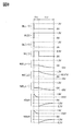
- FIG. 8 is a timing chart illustrating an operation of writing information to a memory cell.
- 9A and 9B are diagrams illustrating an operation of writing information to a memory cell.
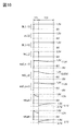
- FIGS. 10 is a timing chart illustrating an operation of writing information to a memory cell.
- FIGS. 11A to 11C are diagrams illustrating an operation of writing information to a memory cell.
- FIG. 12 is a timing chart illustrating an operation of writing information to a memory cell.
- FIGS. 13A and 13B are diagrams illustrating the relationship between the distance between adjacent sub-cell arrays and the holding potential of node ND.
- FIGS. 14A and 14B are diagrams illustrating a circuit configuration example of a dummy memory cell.
- FIGS. 15A and 15B are diagrams illustrating a circuit configuration example of a dummy memory cell.
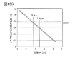
- FIGS. 16A and 16B are diagrams illustrating the relationship between the pitch of the memory cells and the holding potential of the node ND.
- FIGS. 17A and 17B are diagrams illustrating the relationship between the height of the word line and the holding potential of the node ND.
- FIGS. 18A and 18B are diagrams illustrating the operation of writing information to a memory cell.
- FIG. 19 is a diagram illustrating an operation of writing information to a memory cell.
- FIG. 20 is a timing chart illustrating an operation of writing information to a memory cell.
- 21A and 21B are diagrams illustrating the relationship between the information retention time and the leakage current of the capacitor.
- FIG. 22 is a cross-sectional view of the storage device.
- FIG. 23 is a cross-sectional view of the storage device.
- FIG. 24 is a cross-sectional view of the storage device.
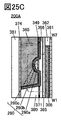
- 25A to 25C are diagrams illustrating an example of a transistor.
- 26A to 26C are diagrams illustrating an example of a transistor.
- 27A and 27B are diagrams illustrating an electronic component.
- FIG. 28 illustrates an electronic device.
- 29A to 29E are diagrams illustrating electronic devices.
- 30A to 30C are diagrams illustrating electronic devices.
- 31A to 31C are diagrams illustrating electronic devices.
- H level also referred to as “VDD” or “H potential”
- L level also referred to as “VSS” or “L potential”.
- a voltage refers to a potential difference between two points, and a potential refers to electrostatic energy (electric potential energy) of a unit charge in an electrostatic field at a certain point.
- a potential difference between a potential at a certain point and a reference potential is simply referred to as a potential or a voltage, and the potential and the voltage are often used as synonyms. Therefore, in this specification and the like, a potential may be read as a voltage or a voltage may be read as a potential unless otherwise specified.
- a metal oxide is an oxide of a metal in a broad sense. Metal oxides are classified into oxide insulators, oxide conductors (including transparent oxide conductors), oxide semiconductors, and the like. For example, in the case where a metal oxide is used for a semiconductor layer of a transistor, the metal oxide may be referred to as an oxide semiconductor in some cases.
- the term “OS transistor” can be referred to as a transistor including a metal oxide or an oxide semiconductor.
- a metal oxide containing nitrogen may be collectively referred to as a metal oxide.
- the threshold voltage (also referred to as “Vth”) is higher than 0V.
- Embodiment 1 In Embodiment, a memory device according to one embodiment of the present invention will be described.
- FIG. 1 is a block diagram illustrating a configuration example of a storage device 100 according to one embodiment of the present invention.
- the storage device 100 includes an input / output circuit 111 (IO @ Circuit), a control circuit 112 (Controller), an I2C receiver 113 (I2C @ Receiver), a setting register 114 (Setting @ Register), an LVDS circuit 115 (transfer circuit LVDS_rx), and an LVDS circuit 116 ( It has a transfer circuit LVDS_tx), a decoder 117 (Decoder), a storage block array 210 (Memory @ Block @ Array), and a negative voltage generation circuit 218.
- the control circuit 112 includes a register 118 (Reg_r) and a register 119 (Reg_w).
- the storage block array 210 has n (n is an integer of 1 or more) storage blocks 211 (Memory @ Block).
- the first storage block 211 is referred to as a storage block 211_1
- the i-th storage block 211 (i is an integer from 1 to n) is referred to as a storage block 211_i.
- the input / output circuit 111 has a function of transmitting / receiving a signal to / from an external device.
- the operating conditions and the like of the storage device 100 are determined by the setting parameters stored in the setting register 114.
- the setting parameters are written to the setting register 114 via the input / output circuit 111 and the I2C receiver 113. Note that the I2C receiver 113 may be omitted depending on the purpose or use.
- the control circuit 112 has a function of processing a setting parameter and an external command signal to determine an operation mode of the storage device 100.
- the control circuit 112 has a function of generating various control signals and controlling the operation of the entire storage device 100.
- a reset signal res, an address signal ADDR [16: 0], a row address identification signal RAS (Row @ Address @ Strobe), and a column address identification signal CAS (Column @ Address @ Strobe) are sent from the outside to the control circuit 112 via the input / output circuit 111.
- a write control signal WE Write @ Enable
- a data read clock signal clk_r is supplied to the control circuit 112 via the LVDS circuit 115.
- a clock signal for data write clk_w and read data RDATA [7: 0] are supplied from the control circuit 112 to the input / output circuit 111.
- the data write clock signal clk_w is supplied to the input / output circuit 111 via the LVDS circuit 116.
- the LVDS circuit 115 and the LVDS circuit 116 are transfer circuits that operate according to the LVDS (Low voltage differential differential) standard. Note that one or both of the LVDS circuit 115 and the LVDS circuit 116 may be omitted depending on the purpose or use.
- the write data WDATA [7: 0] is transferred in synchronization with the data write clock signal clk_w, and is held in the register 119 in the control circuit 112.
- the control circuit 112 has a function of supplying the data held in the register 119 to the storage block array 210.
- the data read from the storage block array 210 is held in the register 118 in the control circuit 112 as read data RDATA [7: 0].
- the control circuit 112 has a function of transferring the read data RDATA [7: 0] to the input / output circuit 111 in synchronization with the data read clock signal clk_r.
- control circuit 112 controls the column address signal C_ADDR [6: 0], the column selection enable signal CSEL_EN, the data latch signal DLAT, the global write enable signal GW_EN, the global read enable signal GR_EN, the global sense amplifier enable signal GSA_EN, and the global equalize enable. It has a function of outputting a signal GEQ_ENB, a local sense amplifier enable signal LSA_EN, a local equalize enable signal LEQ_ENB, a word line address select signal WL_ADDR [7: 0], and the like.
- the column address signal C_ADDR and the column selection enable signal CSEL_EN are supplied to the decoder 117.
- FIG. 2A is a block diagram illustrating a configuration example of the storage block 211_i.
- FIG. 2B is a perspective block diagram illustrating a configuration example of a local sense amplifier array 214 (Local Sense Amplifier Array) and a cell array 221 (Cell Array) included in the storage block 211_i. Also, arrows indicating the X direction, the Y direction, and the Z direction are given in FIG. 2B and the like. The X direction, the Y direction, and the Z direction are directions orthogonal to each other.
- the storage block 211 — i includes a word line driver 212 (WL Driver), a local sense amplifier driver 213 (LSA Driver), a local sense amplifier array 214, a global sense amplifier 215 (Global SA), a read / write selector 216 (R / W Selector), And a cell array 221.
- WL Driver word line driver
- LSA Driver local sense amplifier driver
- Global SA global sense amplifier
- R / W Selector read / write selector
- the data latch signal DLAT, the global write enable signal GW_EN, and the global read enable signal GR_EN are supplied to the read / write selector 216.
- the global sense amplifier enable signal GSA_EN and the global equalize enable signal GEQ_ENB are supplied to the global sense amplifier 215.
- the local sense amplifier enable signal LSA_EN and the local equalize enable signal LEQ_ENB are supplied to the local sense amplifier array 214.
- the word line address selection signals WL_ADDR [7: 0] are supplied to the word line driver 212.
- the local sense amplifier array 214 has a plurality of sense amplifiers 127 (Sense @ Amplifier) arranged in a matrix of f rows and g columns (f and g are both integers of 1 or more).
- the sense amplifier 127 in the first row and first column is referred to as a sense amplifier 127 [1, 1].
- the sense amplifier 127 at the k-th row and the h-th column (k is an integer of 1 or more and f or less; h is an integer of 1 or more and g or less) is referred to as a sense amplifier 127 [k, h].
- the cell array 221 is provided above the local sense amplifier array 214. By providing the cell array 221 so as to overlap the local sense amplifier array 214, the length of the bit line can be reduced.
- the cell array 221 has a plurality of memory cells 10 arranged in a matrix of p rows and q columns (p and q are both integers of 1 or more).
- the memory cell 10 in the first row and the first column is referred to as a memory cell 10 [1, 1].
- the memory cell 10 at the j-th row and the t-th column (j is an integer of 1 or more and p or less; t is an integer of 1 or more and q or less) is referred to as a memory cell 10 [j, t].
- the memory cell 10 functions as a storage element.
- the cell array 221 includes a plurality of word lines WL and wirings BGL extending in the X direction (row direction), a plurality of bit lines BL extending in the Y direction (column direction), and a plurality of bit lines BL in the Y direction (column direction). ) Extending to a plurality of bit lines BLB (not shown in FIG. 2B).
- the j-th word line WL (j is an integer of 1 to p) is referred to as a word line WL [j].
- One memory cell 10 is electrically connected to any one of word lines WL extending in the X direction (row direction).
- One memory cell 10 is electrically connected to any one of wirings BGL extending in the X direction (row direction).
- One memory cell 10 is electrically connected to one of the bit line BL and the bit line BLB.
- the cell array 221 includes a plurality of sub cell arrays 223.
- FIG. 2B shows an example in which the cell array 221 includes four sub-cell arrays 223.
- the four sub cell arrays 223 are shown as sub cell arrays 223_1 to 223_4.
- Each of the plurality of sub-cell arrays 223 includes a plurality of memory cells 10. Therefore, the sub cell array can be called a storage element group.
- Adjacent regions 226 are provided between the sub cell arrays 223_1 and 223_2, between the sub cell arrays 223_2 and 223_3, and between the sub cell arrays 223_3 and 223_4, respectively.
- FIG. 3 shows an enlarged view of the region 225 shown in FIG. 2B.
- the region 225 is a region including a part of the sub cell array 223_2, a part of the sub cell array 223_3, and a part of an adjacent region 226 adjacent to both.
- the adjacent region 226 is a region for electrically connecting the word line WL to an upper or lower layer wiring.
- a wiring that runs in parallel with the word line WL is provided above the word line WL, and the word line WL is electrically connected to the wiring in the adjacent region 226, so that the wiring resistance of the word line WL is substantially reduced. Can be smaller.
- FIG. 4A illustrates a circuit configuration example of the memory cell 10 [j, t ⁇ 1], the memory cell 10 [j, t], and the memory cell 10 [j, t + 1] that are electrically connected to the word line WL [j].
- the memory cell 10 has a transistor M1 and a storage capacitor Cs.
- the storage capacitor Cs functions as a storage capacitor.
- FIG. 4A illustrates a transistor having a back gate (a four-terminal transistor, also referred to as a “four-terminal element”) as the transistor M1.
- One of the source and the drain of the transistor M1 is electrically connected to one electrode of the storage capacitor Cs, and the other of the source and the drain of the transistor M1 is electrically connected to the bit line BL (or the bit line BLB).
- the gate of the transistor M1 is electrically connected to the word line WL, and the back gate of the transistor M1 is electrically connected to the wiring BGL.
- the other electrode of the storage capacitor Cs is electrically connected to the wiring CAL.
- a node at which one of the source or the drain of the transistor M1 and one electrode of the storage capacitor Cs are electrically connected is referred to as a node ND.
- a gate and a back gate are provided so as to overlap with each other via a channel formation region of a semiconductor layer. Both the gate and the back gate can function as gates. Therefore, when one is called “back gate”, the other is sometimes called “gate” or "front gate”. One may be referred to as a “first gate” and the other as a “second gate.”
- the back gate may have the same potential as the gate, a ground potential, or an arbitrary potential. Further, the threshold voltage of the transistor can be changed by changing the potential of the back gate independently without interlocking with the gate.
- the back gate furthermore, by setting the gate and the back gate at the same potential, the region where carriers flow in the semiconductor layer becomes larger in the film thickness direction, so that the amount of carrier movement increases. As a result, the on-state current of the transistor increases and the field-effect mobility increases.
- the transistor can have a large on-state current with respect to the occupied area. That is, the area occupied by the transistor can be reduced with respect to the required on-state current. Thus, a highly integrated semiconductor device can be realized.
- the wiring BGL functions as a wiring for applying a potential to the back gate of the transistor M1.
- the threshold voltage of the transistor M1 can be increased or decreased.
- Writing and reading of data are performed by applying a high-level potential (eg, 3.3 V) to the word line WL, turning on the transistor M1, and electrically connecting the bit line BL to the node ND.
- a low-level potential is applied to the word line WL, so that the transistor M1 is turned off.
- the low-level potential may be, for example, a reference potential or a negative potential.
- a negative potential refers to a potential lower than a reference potential. Therefore, when the reference potential is 0 V, the negative potential is a potential lower than 0 V.
- a large negative potential” or “a large negative potential” means that the potential difference between the reference potential and the negative potential is large.
- Negative potential is small” or “small negative potential” means that the potential difference between the reference potential and the negative potential is small.
- the wiring CAL functions as a wiring for applying a predetermined potential to the other electrode of the storage capacitor Cs. It is preferable to apply a fixed potential to the wiring CAL.
- the memory cell 10 described in this embodiment is a DRAM (Dynamic Random Access Memory) type memory element.
- DRAM Dynamic Random Access Memory
- the transistor M1 included in the memory cell 10 [j, t] may be referred to as a transistor M1 [j, t].
- the storage capacitor Cs included in the memory cell 10 [j, t] may be referred to as a storage capacitor Cs [j, t].
- the circuit diagram shown in FIG. 4A can be shown as in FIG. 4B.
- an oxide semiconductor which is one kind of metal oxide be used for a semiconductor layer where a channel of the transistor M1 is formed.
- a transistor in which a semiconductor layer in which a channel is formed includes an oxide semiconductor is also referred to as an “OS transistor”.
- oxide semiconductor indium, element M (element M is aluminum, gallium, yttrium, copper, vanadium, beryllium, boron, titanium, iron, nickel, germanium, zirconium, molybdenum, lanthanum, cerium, neodymium, hafnium,
- oxide semiconductor is preferably a metal oxide containing indium, gallium, and zinc.
- the OS transistor has a characteristic of extremely low off-state current.
- the leakage current (leakage current) of the transistor M1 can be extremely low. That is, the written data can be held for a long time by the transistor M1. Therefore, the frequency of refreshing the storage element can be reduced. Further, the refresh operation of the storage element can be made unnecessary. Further, since the leakage current is extremely low, it is possible to easily realize a storage element which holds multi-valued data or analog data.
- DOSRAM Dynamic Oxide Semiconductor Random Access Memory
- FIGS. 5A and 5B show structural examples of the transistor M1 [j, t] and the transistor M1 [j, t + 1].
- FIG. 5A is a perspective view of the transistor M1 [j, t] and the transistor M1 [j, t + 1], and
- FIG. 5B is a top view. Note that some components are omitted for easy understanding of the drawings.
- the transistor M1 [j, t] includes the oxide layer 261 (the oxide layer 261a, the oxide layer 261b, and the oxide layer 261c).
- the oxide layer 261 functions as a semiconductor layer.
- the conductive layer 342 (the conductive layer 342a and the conductive layer 342b) is provided over the oxide layer 261b.
- One of the conductive layers 342a and 342b functions as a source electrode, and the other functions as a drain electrode.
- a conductive layer 360, an insulating layer 349, and an oxide layer 261c are provided between the conductive layers 342a and 342b.
- the insulating layer 349 has a region overlapping the side surface of the conductive layer 360 and a region overlapping the bottom surface of the conductive layer 360.
- the oxide layer 261 c has a region overlapping with the side surface of the conductive layer 360 with the insulating layer 349 interposed therebetween, and a region overlapping with the bottom surface of the conductive layer 360 with the insulating layer 349 interposed therebetween.
- the oxide layer 261c has a region in contact with the oxide layer 261b.
- a region overlapping with the oxide layer 261c functions as a gate electrode.
- An insulating layer 366 is provided below the oxide layer 261a, and an insulating layer 365 is provided below the insulating layer 366.
- the conductive layer 305 is provided below the insulating layer 365.
- the conductive layer 305 is provided at a position overlapping with the conductive layer 360.
- the conductive layer 305 functions as a wiring BGL [j]. Further, the conductive layer 305 functions as a back gate electrode of the transistor M1 [j, t].
- the conductive layer 360 functions as the word line WL [j]. Further, the conductive layer 360 functions as a gate electrode of the transistor M1 [j, t].
- the insulating layer 349 functions as a gate insulating layer of the transistor M1 [j, t].
- the transistor M1 [j, t + 1] has a structure similar to that of the transistor M1 [j, t]. Therefore, the conductive layer 360 functions as a gate electrode of the transistor M1 [j, t + 1].
- the insulating layer 349 functions as a gate insulating layer of the transistor M1 [j, t + 1]. The transistor structure will be described later in detail.
- the oxide layer 261c overlaps with the word line WL [j] through the insulating layer 349, and the oxide layer 261c includes the oxide layer 261b of the transistor M1 [j, t] and the transistor M1 [j, [t + 1] is in contact with the oxide layer 261b. Therefore, a parasitic transistor Trp may be generated between the transistor M1 [j, t] and the transistor M1 [j, t + 1].
- the oxide layer 261b of the transistor M1 [j, t] and the oxide layer 261b of the transistor M1 [j, t + 1] are electrically connected to each other, and therefore, along the word line WL [j]. A leak path is likely to occur (see FIG. 5B).
- parasitic capacitance Cp When the parasitic transistor Trp occurs, a parasitic capacitance Cp occurs in which the word line WL [j] is one electrode and the oxide layer 261c is the other electrode (parasitic node NDp).
- the parasitic capacitance Cp corresponds to the gate capacitance of the parasitic transistor Trp (see FIG. 5A).
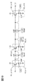
- FIG. 5C is a circuit diagram showing the memory cell 10 [j, t], the memory cell 10 [j, t + 1], the parasitic transistor Trp, and the parasitic capacitance Cp. Note that in this embodiment, it is assumed that a negative voltage is always supplied to the wiring BGL [j]. Therefore, in the following circuit diagrams and the like, description of the wiring BGL [j] may be omitted in order to make the drawings easy to understand. For example, in FIG. 5C, the description of the wiring BGL is omitted.
- the parasitic transistor Trp is divided into two.
- the parasitic transistor Trp and the parasitic capacitance Cp are indicated by broken lines.
- the field effect mobility of the parasitic transistor Trp is significantly smaller than the field effect mobility of the transistor M1. Therefore, when the data writing speed to the memory cell 10 is high (when the operating frequency is high), the influence of the above-described leak path is negligible. On the other hand, when the data writing speed to the memory cell 10 is low (when the operating frequency is low, for example, when the operating frequency is 10 MHz or less), the influence of the leak path becomes remarkable, and the data writing to the memory cell 10 is insufficient. It may be.
- FIG. 6A is a circuit diagram showing the memory cell 10 [j, t-1], the memory cell 10 [j, t], the memory cell 10 [j, t + 1], the parasitic transistor Trp, and the parasitic capacitance Cp.
- the memory cell 10 [j, t-1] and the memory cell 10 [j, t] are memory cells included in the sub cell array 223_2, and the memory cell 10 [j, t + 1] is a memory cell included in the sub cell array 223_3. .
- a parasitic transistor, a parasitic capacitance, and a parasitic node generated between the memory cell 10 [j, t-1] and the memory cell 10 [j, t] are referred to as a parasitic transistor TrpA, a parasitic capacitance CpA, and a parasitic node NDpA, respectively. It is shown. Further, a parasitic transistor, a parasitic capacitance, and a parasitic node generated between the memory cell 10 [j, t] and the memory cell 10 [j, t + 1] are denoted as a parasitic transistor TrpB, a parasitic capacitance CpB, and a parasitic node NDpB, respectively. .
- the potential corresponding to “0” in the information written to the memory cell 10 is set to 0 V or more and less than 0.6 V, and the potential corresponding to “1” is set to 0.6 V or more and 1.2 V or less.
- the storage capacitance Cs is 3.5 fF
- the parasitic capacitance CpA is 1.0 fF
- the parasitic capacitance CpB is 3.0 fF.
- the potential WLH supplied to the word line WL is set to 3.3 V to turn on the transistor M1 (conductive state)
- the potential WLL supplied to the word line WL is set to 0 V to turn off (non-conductive state) the transistor M1.
- Vth of the parasitic transistors TrpA and TrpB is set to 1.5V.
- FIG. 8 is a timing chart for explaining an information writing operation.
- reference numerals may be omitted to make the drawings easier to see. 6B, 7A, and 7B can be understood by referring to FIG. 6A and the like.
- the fluctuating potential is indicated by surrounding it with a black line.
- FIG. 7A illustrates a state immediately after the transistors M1 [j, t ⁇ 1], M1 [j, t], and M1 [j, t + 1] are turned off (a state immediately after the start of the period T12). I have.
- the field-effect mobility of the parasitic transistor Trp is significantly smaller than the field-effect mobility of the transistor M1.
- the node ND [j, t-1], the node ND [j, t], the node ND [j, t + 1], the parasitic node NDpA, and the parasitic node NDpB Charge transfer (charge redistribution) occurs. The movement of the charge continues until the potentials of the parasitic nodes NDpA and NDpB become ⁇ 1.5 V.
- the potentials of the nodes ND [j, t-1], ND [j, t] and ND [j, t + 1] after the end of the charge transfer are the holding capacitance Cs and the capacitances of the parasitic capacitances CpA and CpB. Is determined.
- the potentials of the nodes ND [j, t-1] and ND [j, t + 1] after the end of the charge transfer become lower than 0V, and the potential of the node ND [j, t] becomes 0.51V. (See FIGS. 7B and 8).
- the data stored in the memory cell 10 is recognized as “0”. Also, when the potential of the node ND is 0.51 V at the time of reading data, the data stored in the memory cell 10 is recognized as “0”. That is, data is normally written in the memory cells 10 [j, t-1] and 10 [j, t + 1], but data is normally written in the memory cells 10 [j, t]. Will not be.
- FIGS. 9A, 9B, and 10 "1" is set in the memory cell 10 [j, t-1], the memory cell 10 [j, t], and the memory cell 10 [j, t + 1].
- FIGS. 9A, 9B, and 10 are timing charts for explaining an information writing operation.
- 1.2 V is supplied to the bit line BL [t-1], the bit line BL [t], and the bit line BL [t + 1], and 3.3 V is supplied to the word line WL [j].
- the transistor M1 [j, t-1], the transistor M1 [j, t], and the transistor M1 [j, t + 1] are turned on, and the nodes ND [j, t-1] and ND [j, t] , And the node ND [j, t + 1] is written with 1.2 V (see FIGS. 9A and 10).
- the parasitic node NDpA immediately after the potential of the word line WL [j] changes from 0 V to 3.3 V.
- the potential of the parasitic node NDpB becomes 1.8 V.
- the potentials of the parasitic nodes NDpA and NDpB both become 1.2V.
- 0 V is supplied to the word line WL [j] to turn off the transistor M1 [j, t-1], the transistor M1 [j, t], and the transistor M1 [j, t + 1]. .
- the potentials of the nodes ND [j, t-1], ND [j, t] and ND [j, t + 1] after the end of the charge transfer are the holding capacitance Cs and the capacitances of the parasitic capacitances CpA and CpB. Is determined.
- the potential of the node ND [j, t] becomes 0.85 V (see FIGS. 9B and 10).
- the potential of the node ND [j, t-1] after the end of the charge transfer is 0.86 V or more (see FIG. 12) and less than 1.2 V due to the influence of the node ND [j, t-2].
- the potential of the node ND [j, t + 1] after the end of the charge transfer becomes 0.86 V or more and less than 1.2 V under the influence of the node ND [j, t + 2].
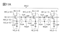
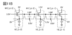
- FIG. 11A is a circuit diagram showing the memory cell 10 [j, t-3], the memory cell 10 [j, t-2], the memory cell 10 [j, t-1], the parasitic transistor TrpA, and the parasitic capacitance CpA. is there.
- the memory cell 10 [j, t-3], the memory cell 10 [j, t-2], and the memory cell 10 [j, t-1] are memory cells included in the sub cell array 223_2.
- the capacitance of the parasitic capacitance CpA generated between the memory cell 10 [j, t-3] and the memory cell 10 [j, t-2], the memory cell 10 [j, t-2] and the memory cell 10 [j, t-2] is set to 1.0 fF.
- FIG. 11B, FIG. 11C, and FIG. 12 are timing chart for explaining an information writing operation.
- 0 V is supplied to the word line WL [j] to turn on the transistor M1 [j, t-3], the transistor M1 [j, t-2], and the transistor M1 [j, t-1]. Turn off.
- the potential of the parasitic node NDpA immediately after supplying 0 V to the word line WL [j] becomes -2.7 V.
- the potential of the parasitic node NDpA becomes -1.5 V due to the redistribution of the electric charge.
- the capacitance of the parasitic capacitance CpA generated between the memory cell 10 [j, t-3] and the memory cell 10 [j, t-2] and the memory cell 10 [j, t-2] is 1.0 fF in each case. Therefore, in this circuit configuration, the potentials of the nodes ND [j, t-3] and ND [j, t-1] after the end of the charge transfer become lower than 0 V, and the potentials of the nodes ND [j, t-2] become lower. The potential becomes 0.86 V (see FIGS. 11C and 12).
- the data stored in the memory cell 10 is recognized as “0”.
- the potential of the node ND is 0.86 V at the time of data reading, the data stored in the memory cell 10 is recognized as "1".
- a write error easily occurs due to the influence of the parasitic capacitance generated in the adjacent region 226. That is, by reducing the parasitic capacitance of the adjacent region 226, occurrence of a writing error can be suppressed.
- the parasitic capacitance associated with the word line WL between the adjacent memory cells 10 changes in proportion to the length of the word line WL between the adjacent memory cells 10. Therefore, the parasitic capacitance can be reduced by shortening the length of the word line WL between the adjacent memory cells 10.
- the memory cell 10 [j, t-1] in the same sub-cell array starts from the gate electrode of the transistor M1 [j, t-1] of the memory cell 10 [j, t-1] in the sub-cell array.
- the distance DA is the length of the word line WL [j] to the gate electrode of the transistor M1 [j, t] included in [t].
- the memory cell 10 [j, t] the memory cell 10 [j, The length of the word line WL [j] to the gate electrode of the transistor M1 [j, t + 1] included in [t + 1] is defined as a distance DB.
- the distance DB can be said to be the shortest distance between adjacent sub-cell arrays.
- the distance DA can be said to be the shortest distance from the adjacent bit line BL [t-1] to the bit line BL [t] in the sub-cell array.
- the distance DB can be said to be the shortest distance from the bit line BL [t] arranged at the end of the sub cell array to the bit line BL [t + 1] arranged at the end of the adjacent sub cell array.
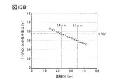
- FIG. 13B is a graph in which the relationship between the distance DB and the holding potential of the node ND [j, t] is calculated when the above-described information writing operation is performed.
- the capacitance of the storage capacitor Cs is 3.5 fF
- the capacitance of the parasitic capacitance CpA is 1.0 fF
- the distance DA is calculated as 1.4 ⁇ m.
- FIG. 13B shows that the distance DB needs to be 3.5 ⁇ m or less in order to make the holding potential of the node ND [j, t] in which “1” is written 0.6 V or more.
- the holding potential of the node ND [j, t] to which "1" is written be 0.75 V or more.
- FIG. 13B shows that the distance DB needs to be 2.3 ⁇ m or less in order to make the holding potential of the node ND [j, t] 0.75 V or more.
- the distance DB is preferably at least 1 and at most 3.5 times the distance DA, more preferably at least 1 and at most 2.3 times.
- a dummy memory cell 10d may be provided in the adjacent region 226.
- the dummy memory cell 10d has a transistor M1d and a storage capacitor Csd.
- One of a source and a drain of the transistor M1d is electrically connected to one electrode of the storage capacitor Csd through the node NDd.
- the other electrode of the storage capacitor Csd is electrically connected to the wiring CAL.
- the gate of the transistor M1d is electrically connected to the word line WL [j].
- VDD (1.2 V in this embodiment) is supplied to the other of the source and the drain of the transistor M1d.
- the parasitic capacitance CpB can be divided into the parasitic capacitance CpB1 and the parasitic capacitance CpB2.
- the parasitic capacitance CpB can be halved.
- the parasitic transistor TrpB can be divided into a parasitic transistor TrpB1 and a parasitic transistor TrpB2.
- the parasitic node NDpB can be divided into a parasitic node NDpB1 and a parasitic node NDpB2.
- a plurality of dummy memory cells 10d may be provided in the adjacent region 226.
- the node NDd may be in a floating state without providing the storage capacitor Csd in the dummy memory cell 10d.
- VDD may be supplied to the source and the drain of the transistor M1d without providing the storage capacitor Csd in the dummy memory cell 10d.
- a write error of the storage device 100 can be reduced.
- the reliability of the storage device 100 can be improved.
- the distance DA can be regarded as a pitch (arrangement period) of the memory cells 10 arranged in a matrix.
- FIG. 16B is a graph in which the relationship between the distance DA and the holding potential of the node ND [j, t ⁇ 2] is calculated when the capacitance of the holding capacitor Cs is 3.5 fF. From FIG. 16B, it can be seen that the distance DA needs to be 2.5 ⁇ m or less in order to make the holding potential of the node ND [j, t ⁇ 2] in which “1” is written 0.6 V or more. Further, it can be seen that the distance DA needs to be 1.8 ⁇ m or less in order to make the holding potential of the node ND [j, t ⁇ 2] in which “1” is written 0.75 V or more.
- the pitch of the memory cells 10 arranged in a matrix is set to 2.5 ⁇ m or less. There is a need to. Further, in order to make the holding potential of the node ND [j, t ⁇ 2] in which “1” is written 0.75 V or more, the pitch of the memory cells 10 arranged in a matrix is made 1.8 ⁇ m or less. There is a need.
- FIG. 17A is a cross-sectional view of a Y1-Y2 portion shown by a dashed line in FIG. 5B.
- the capacitances of the parasitic capacitances CpA and CpB are proportional to the area where the word line WL [j] and the oxide layer 261c overlap.
- a negative voltage is supplied to the wiring BGL [j]
- carriers are less likely to be generated in the oxide layer 261c overlapping the bottom surface of the word line WL [j]. Accordingly, when the distance DA and the distance DB are constant, the capacitance H of the parasitic capacitance CpA and the parasitic capacitance CpB can be reduced by reducing the height H of the word line WL [j] illustrated in FIG. 5B.
- FIG. 17B is a graph showing the relationship between the height H of the word line WL [j] and the holding potential of the node ND [j, t] when the above-described information writing operation is performed.
- the graph shown in FIG. 17B shows that the capacitance of the storage capacitor Cs is 3.5 fF, the capacitance of the parasitic capacitance CpA when the height H is 120 nm is 1.0 fF, and the parasitic capacitance CpB when the height H is 120 nm.
- the capacitance of 3.0 fF a distance DA of 1.4 ⁇ m
- a distance DB of 4.2 ⁇ m.
- the height H needs to be 105 nm or less in order to make the holding potential of the node ND [j, t] in which “1” is written 0.6 V or more. Further, it can be seen that the height H needs to be 79 nm or less in order to make the holding potential of the node ND [j, t] in which “1” is written 0.75 V or more.
- the amount of charge transfer between the node ND and the parasitic node NDp can be reduced. Therefore, a decrease in the holding potential of the node ND can be reduced.
- Vth of the parasitic transistor Trp can be increased.
- the electron affinity of the oxide layer 261c is preferably smaller than the electron affinity of the oxide layer 261b.
- an In-M-Zn oxide (element M is gallium, yttrium, tin, copper, vanadium, beryllium, boron, titanium, iron, nickel, germanium, zirconium, molybdenum, lanthanum, cerium, neodymium , Hafnium, tantalum, tungsten, magnesium, or the like), when the metal oxide used for the oxide layer 261c has an atomic ratio of the element M to In used for the oxide layer 261b. It is preferable that the ratio of the number of atoms of the element M to In in the metal oxide is larger than that.
- an M-Zn oxide or an M oxide is preferably used as a metal oxide used for the oxide layer 261c.
- Vth of the parasitic transistor Trp By increasing Vth of the parasitic transistor Trp, a write error of the storage device 100 can be reduced. Therefore, the reliability of the storage device 100 can be improved.
- the potential WLH and the potential WLL may be lowered without changing the potential difference between the potential WLH and the potential WLL supplied to the word line WL. Writing errors in the storage device 100 can be reduced.
- FIGS. 18A, 18B, 19, and 20, "0" is assigned to memory cell 10 [j, t-1], "1" is assigned to memory cell 10 [j, t], and memory cell 10 [j, A case where “0” is written to [t + 1] will be described.
- FIG. 20 is a timing chart for explaining an information writing operation.
- 18A, 18B, and 19 are circuit diagrams corresponding to FIG. 6A. 18A, FIG. 18B, and FIG. 19, reference numerals may be omitted in some cases in order to make the drawings easy to see. 18A, FIG. 18B, and FIG. 19 can be understood by referring to FIG. 6A and the like.
- the node ND [j, t-1], the node ND [j, t], the node ND [j, t + 1], the parasitic node NDpA, and the parasitic node NDpB Charge transfer (charge redistribution) occurs. Since the potential of the word line WL [j] is ⁇ 0.3 V, the movement of the charge continues until the potentials of the parasitic nodes NDpA and NDpB become ⁇ 1.8 V.
- the potentials of the nodes ND [j, t-1], ND [j, t] and ND [j, t + 1] after the end of the charge transfer are the holding capacitance Cs and the capacitances of the parasitic capacitances CpA and CpB. Is determined.
- the potentials of the nodes ND [j, t ⁇ 1] and ND [j, t + 1] after the end of the charge transfer become lower than 0V, and the potential of the node ND [j, t] becomes 0.69V. (See FIGS. 19 and 20).
- the amount of charge moving between the parasitic nodes NDpA and NDpB is reduced, and the nodes ND [j, t-1], ND [j, t], and ND [j, t + 1] ] Can be reduced.
- a writing error of the storage device 100 can be further reduced.
- the potential WLH is 2.8 V and the potential WLL is -0.5 V
- the potential of the node ND [j, t] to which data "1" is written can be 0.8 V.
- the potential WLH needs to be equal to or higher than the potential obtained by adding Vth of the transistor M1 to the potential supplied to the bit line BL.
- Vth of the transistor M1 is 0.5 V
- the potential WLH needs to be 1.7 V or more.
- This embodiment can be implemented in appropriate combination with the structures described in the other embodiments and the like.
- FIG. 21A shows a circuit configuration example of the memory cell 10.
- the memory cell 10 has a transistor M1 and a storage capacitor Cs.
- One of a source and a drain of the transistor M1 is electrically connected to one electrode of the storage capacitor Cs, and the other of the source and the drain of the transistor M1 is electrically connected to one of the bit lines BL and a gate of the transistor M1.
- a node at which one of the source or the drain of the transistor M1 and one electrode of the storage capacitor Cs are electrically connected is referred to as a node ND.
- the wiring CAL functions as a wiring for applying a predetermined potential to the other electrode of the storage capacitor Cs. It is preferable to apply a fixed potential (for example, 0 V) to the wiring CAL.
- Data writing is performed by applying a high-level potential to the word line WL to make the transistor M1 conductive and electrically connecting the bit line BL to the node ND.
- a low-level potential eg, 0 V or a negative potential
- the data written in the memory cell 10 is held as electric charge at the node ND.
- an OS transistor is preferably used as the transistor M1.
- the OS transistor has a characteristic of extremely low off-state current.
- the leakage current of the transistor M1 can be extremely low. Therefore, data written to the node ND can be held for a long time.
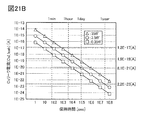
- FIG. 21B is a graph illustrating the relationship between the retention time of data written to the node ND and CsI_leak when the capacitance value of the storage capacitor Cs is 35 fF, 3.5 fF, or 0.35 fF. Note that in the present embodiment, the time until the potential of the node ND decreases by 0.2 V is referred to as a holding time.
- CsI_leak when the capacitance value of the storage capacitor Cs is 3.5 fF, it is necessary to set CsI_leak to 1.2 ⁇ 10 ⁇ 17 A or less in order to set the storage time to 1 minute. . Similarly, in order to set the holding time to one hour, it is understood that CsI_leak needs to be 1.9 ⁇ 10 ⁇ 19 A or less. Similarly, it can be seen that it is necessary to set CsI_leak to 8.1 ⁇ 10 ⁇ 21 A or less in order to set the holding time to one day. Similarly, it can be seen that CsI_leak needs to be 2.2 ⁇ 10 ⁇ 23 A or less in order to make the retention time one year.
- CsI_leak by increasing the capacitance value of the storage capacitor Cs ten times, the allowable current of CsI_leak can be increased ten times. For example, when the capacitance value of the storage capacitor Cs is 35 fF, in order to set the storage time to one hour, CsI_leak may be 1.9 ⁇ 10 ⁇ 18 A or less.
- CsI_leak When the capacitance value of the storage capacitor Cs is increased by 0.1, the allowable current of CsI_leak also needs to be increased by 0.1. For example, when the capacitance value of the storage capacitor Cs is 0.35 fF, CsI_leak needs to be 1.9 ⁇ 10 ⁇ 20 A or less in order to set the storage time to one hour.
- This embodiment can be implemented in appropriate combination with the structures described in the other embodiments and the like.
- the 212, the local sense amplifier driver 213, the sense amplifier 127, the global sense amplifier 215, the read / write selector 216, and the like may require high current driving capability and / or high-speed operation. In this case, it is preferable to use a Si transistor as a transistor constituting these circuits. Further, it is preferable to use an OS transistor as a transistor included in the memory cell 10.
- the OS transistor and the Si transistor can be stacked. Therefore, an integrated circuit including an OS transistor can be provided over an integrated circuit including a Si transistor.
- the size of the storage device 100 can be reduced. In other words, the area occupied by the storage device 100 can be reduced.
- an integrated circuit including the memory cell 10 may be provided over an integrated circuit including the sense amplifier 127.
- the size of the storage device 100 can be reduced.
- the size of the semiconductor device including the storage device 100 can be reduced.
- the area occupied by the storage device 100 can be reduced.
- the area occupied by the semiconductor device including the storage device 100 can be reduced.
- FIG. 22 shows a partial cross section of the storage device 100.
- a local sense amplifier array 214 and a cell array 221 are stacked on a substrate 231.
- circuits other than the cell array 221 are provided on the substrate 231 similarly to the local sense amplifier array 214.
- FIG. 22 illustrates the case where a single crystal semiconductor substrate (eg, a single crystal silicon substrate) is used as the substrate 231.
- the source, the drain, and the channel of the transistor included in the local sense amplifier array 214 are formed in part of the substrate 231.
- the cell array 221 includes a thin film transistor (for example, an OS transistor).
- the local sense amplifier array 214 has a transistor 233a, a transistor 233b, and a transistor 233c on a substrate 231.
- FIG. 22 illustrates a cross section of the transistor 233a, the transistor 233b, and the transistor 233c in the channel length direction.
- the channels of the transistor 233a, the transistor 233b, and the transistor 233c are formed in part of the substrate 231.
- a single crystal semiconductor substrate is preferably used as the substrate 231.
- the transistor 233a, the transistor 233b, and the transistor 233c are electrically separated from other transistors by the element separation layer 232.
- the element isolation layer can be formed by a LOCOS (Local Oxidation of Silicon) method, an STI (Shallow Trench Isolation) method, or the like.
- An insulating layer 234, an insulating layer 235, and an insulating layer 237 are provided over the transistor 233a, the transistor 233b, and the transistor 233c, and the electrode 238 is embedded in the insulating layer 237.
- the electrode 238 is electrically connected to one of the source and the drain of the transistor 233a through the contact plug 236.
- An insulating layer 239, an insulating layer 240, and an insulating layer 241 are provided over the electrode 238 and the insulating layer 237, and the electrode 242 is embedded in the insulating layer 239, the insulating layer 240, and the insulating layer 241. .
- the electrode 242 is electrically connected to the electrode 238.
- An insulating layer 243 and an insulating layer 244 are provided over the electrode 242 and the insulating layer 241, and the electrode 245 is embedded in the insulating layer 243 and the insulating layer 244.
- the electrode 245 is electrically connected to the electrode 242.
- An insulating layer 246 and an insulating layer 247 are provided over the electrode 245 and the insulating layer 244, and the electrode 249 is embedded in the insulating layer 246 and the insulating layer 247.
- the electrode 249 is electrically connected to the electrode 245.
- the insulating layer 248 and the insulating layer 250 are provided over the electrode 249 and the insulating layer 247, and the electrode 251 is embedded in the insulating layer 248 and the insulating layer 250.
- the electrode 251 is electrically connected to the electrode 249.
- the cell array 221 is provided on the local sense amplifier array 214.
- the cell array 221 includes a transistor 200 and a capacitor 220.
- FIG. 22 illustrates a cross section of the transistor 200 in the channel length direction.
- the transistor 200 is a transistor having a back gate.
- the transistor 200 corresponds to the transistor M1
- the capacitor 220 corresponds to the storage capacitor Cs.
- an oxide semiconductor which is a kind of metal oxide for a semiconductor layer of the transistor 200. That is, an OS transistor is preferably used as the transistor 200.
- the transistor 200 is provided over the insulating layer 361. Further, an insulating layer 362 is provided over the insulating layer 361. The back gate of the transistor 200 is embedded in the insulating layer 362. The insulating layer 371 and the insulating layer 380 are provided over the insulating layer 362. The gate of the transistor 200 is embedded in the insulating layer 380.
- the insulating layer 374 and the insulating layer 381 are provided over the insulating layer 380.
- the electrode 355 is embedded in the insulating layer 361, the insulating layer 362, the insulating layer 365, the insulating layer 366, the insulating layer 371, the insulating layer 380, the insulating layer 374, and the insulating layer 381.
- the electrode 355 is electrically connected to the electrode 251.
- the electrode 355 can function as a contact plug.
- the electrode 152 is provided over the insulating layer 381.
- the electrode 152 is electrically connected to the electrode 355.
- the insulating layer 272, the insulating layer 273, and the insulating layer 130 are provided over the insulating layer 381 and the electrode 152.
- the capacitor 220 includes the electrode 110 provided in an opening formed in the insulating layer 272 and the insulating layer 273, the insulating layer 130 over the electrode 110 and the insulating layer 273, and the electrode 120 over the insulating layer 130. . At least a part of the electrode 110, at least a part of the insulating layer 130, and at least a part of the electrode 120 are arranged in openings formed in the insulating layers 272 and 273.
- the electrode 110 functions as a lower electrode of the capacitor 220
- the electrode 120 functions as an upper electrode of the capacitor 220
- the insulating layer 130 functions as a dielectric of the capacitor 220.
- the capacitor 220 has a structure in which an upper electrode and a lower electrode are opposed to each other not only on the bottom surface but also on the side surface of the opening of the insulating layer 272 and the insulating layer 273 with a dielectric material interposed therebetween.
- the capacity can be increased. Therefore, the capacitance of the capacitor 220 can be increased as the opening is deepened. By thus increasing the capacitance per unit area of the capacitor 220, miniaturization or high integration of the semiconductor device can be promoted.
- the shape of the opening formed in the insulating layer 272 and the insulating layer 273 as viewed from above may be a quadrangle, a polygon other than the quadrangle, or a shape in which a corner is curved in the polygon. And a circular shape including an ellipse.
- an insulating layer 274 and an insulating layer 154 are provided over the insulating layer 130 and the electrode 120.
- the electrode 271 is embedded in the insulating layer 272, the insulating layer 273, the insulating layer 130, the insulating layer 274, and the insulating layer 154.
- the electrode 271 is electrically connected to the electrode 152.
- the electrode 271 can function as a contact plug.
- An electrode 153 is provided over the insulating layer 154. The electrode 153 is electrically connected to the electrode 271.
- An insulating layer 156 is provided over the insulating layer 154 and the electrode 153.
- FIG. 23 shows a storage device 100A which is a modification of the storage device 100.
- a local sense amplifier array 214A and a cell array 221 are provided in an overlapping manner.
- the local sense amplifier array 214A uses an OS transistor as a transistor such as the transistor 233a and the transistor 233b included in the local sense amplifier array 214.
- the storage device 100 can be a monopolar integrated circuit.
- FIG. 24 shows a storage device 100B which is a modification of the storage device 100A.
- the local sense amplifier array 214A and the cell array 221 can be manufactured over the substrate 231 in the same step. Therefore, the productivity of the semiconductor device can be improved. Further, the production cost of the semiconductor device can be reduced.
- the cooling efficiency of the semiconductor device can be increased as compared with a case where an insulating substrate or the like is used. Therefore, the reliability of the semiconductor device can be improved.
- ⁇ Constituent materials ⁇ ⁇ Substrate> There is no particular limitation on the material used for the substrate. For example, an insulator substrate, a semiconductor substrate, or a conductor substrate may be used.
- the insulator substrate examples include a glass substrate, a quartz substrate, a sapphire substrate, a stabilized zirconia substrate (such as a yttria-stabilized zirconia substrate), and a resin substrate.
- the semiconductor substrate examples include a semiconductor substrate formed using silicon, germanium, or the like, or a compound semiconductor substrate formed using silicon carbide, silicon germanium, gallium arsenide, indium phosphide, zinc oxide, or gallium oxide.
- a semiconductor substrate having an insulator region inside the above-described semiconductor substrate for example, an SOI (Silicon On Insulator) substrate or the like may be used.
- a single crystal semiconductor substrate is preferably used as the substrate.
- the conductor substrate examples include a graphite substrate, a metal substrate, an alloy substrate, and a conductive resin substrate.
- a substrate including a metal nitride, a substrate including a metal oxide, and the like are given.
- a substrate in which an element is provided may be used.
- Elements provided on the substrate include a capacitor, a resistor, a switch, a light-emitting element, a storage element, and the like.
- a semiconductor substrate provided with a semiconductor element such as a strained transistor or a FIN transistor on a semiconductor substrate can also be used. That is, the substrate is not limited to a mere support substrate, and may be a substrate on which devices such as other transistors are formed.
- a material used for the insulating layer examples include an oxide, a nitride, an oxynitride, a nitrided oxide, a metal oxide, a metal oxynitride, and a metal nitrided oxide having an insulating property.
- a problem such as leakage current may occur due to a reduction in the thickness of a gate insulating layer.
- a high-k material is used for the insulating layer functioning as a gate insulating layer, a voltage can be reduced during operation of the transistor while maintaining the physical thickness.
- a material having a low relative dielectric constant for an insulator functioning as an interlayer insulating layer parasitic capacitance generated between wirings can be reduced. Therefore, a material may be selected according to the function of the insulating layer.
- Examples of the insulator having a high relative dielectric constant include gallium oxide, hafnium oxide, zirconium oxide, an oxide containing aluminum and hafnium, an oxynitride containing aluminum and hafnium, an oxide containing silicon and hafnium, and silicon and hafnium. Oxynitride or nitride containing silicon and hafnium.
- Insulators having a low relative dielectric constant include silicon oxide, silicon oxynitride, silicon nitride oxide, silicon nitride, silicon oxide added with fluorine, silicon oxide added with carbon, silicon oxide added with carbon and nitrogen, and empty. There is silicon oxide having a hole, resin, or the like.
- an OS transistor In the case where an OS transistor is used as a transistor, electric characteristics of the transistor can be reduced by surrounding the transistor with an insulating layer having a function of suppressing transmission of impurities such as hydrogen and oxygen (such as the insulating layers 361 and 374). Can be stable.
- the insulator having a function of suppressing transmission of impurities such as hydrogen and oxygen include boron, carbon, nitrogen, oxygen, fluorine, magnesium, aluminum, silicon, phosphorus, chlorine, argon, gallium, germanium, yttrium, and zirconium.
- Lanthanum, neodymium, hafnium, or an insulator containing tantalum may be used as a single layer or a stacked layer.
- an insulator having a function of suppressing transmission of impurities such as hydrogen and oxygen
- a metal oxide such as tantalum oxide, a metal nitride such as aluminum nitride, aluminum titanium nitride, titanium nitride, silicon nitride oxide, or silicon nitride can be used.
- the insulating layer functioning as a gate insulating layer is preferably an insulator having a region containing oxygen released by heating.
- an insulator having a region containing oxygen released by heating For example, with a structure in which silicon oxide or silicon oxynitride having a region containing oxygen released by heating is in contact with the semiconductor layer 260, oxygen vacancies in the semiconductor layer 260 can be compensated.
- a nitrided oxide refers to a compound having a higher nitrogen content than oxygen.
- Oxynitride refers to a compound having a higher oxygen content than nitrogen.
- the content of each element can be measured, for example, by using Rutherford Backscattering (Spectrometry) (RBS).
- the concentration of hydrogen in the insulating layer is preferably reduced in order to prevent an increase in the concentration of hydrogen in the semiconductor layer.
- the concentration of hydrogen in the insulating layer is determined to be not more than 2 ⁇ 10 20 atoms / cm 3 , preferably not more than 5 ⁇ 10 19 atoms / cm 3 by secondary ion mass spectrometry (SIMS: Secondary Ion Mass Spectrometry). It is more preferably at most 1 ⁇ 10 19 atoms / cm 3 , further preferably at most 5 ⁇ 10 18 atoms / cm 3 .
- the concentration of nitrogen in the insulating layer is preferably reduced in order to prevent an increase in the concentration of nitrogen in the semiconductor layer.
- the concentration of nitrogen in the insulating layer is set to 5 ⁇ 10 19 atoms / cm 3 or less, preferably 5 ⁇ 10 18 atoms / cm 3 or less, more preferably 1 ⁇ 10 18 atoms / cm 3 or less in SIMS. More preferably, it is set to 5 ⁇ 10 17 atoms / cm 3 or less.
- the insulating layer which is in contact with the semiconductor layer preferably has few defects.
- a signal observed by electron spin resonance (ESR) be small.
- the above signal includes the E ′ center where the g value is observed at 2.001.
- the E ′ center is caused by dangling bonds of silicon.
- the spin density attributable to the E ′ center is 3 ⁇ 10 17 spins / cm 3 or less, preferably 5 ⁇ 10 16 spins / cm 3 or less.
- a silicon oxide layer or a silicon oxynitride layer may be used.
- a signal due to nitrogen dioxide (NO 2 ) may be observed in addition to the above signal.
- the signal is split into three signals by N nuclear spins, each having a g value of 2.037 or more and 2.039 or less (referred to as a first signal), and a g value of 2.001 or more and 2.003. Or less (referred to as a second signal), and a g value of 1.964 to 1.966 (referred to as a third signal).
- the insulating layer an insulating layer in which the spin density of a signal due to nitrogen dioxide (NO 2 ) is greater than or equal to 1 ⁇ 10 17 spins / cm 3 and less than 1 ⁇ 10 18 spins / cm 3 .
- NO 2 nitrogen dioxide
- nitrogen oxide (NO x ) containing nitrogen dioxide (NO 2 ) forms a level in the insulating layer.
- the level is located in the energy gap of the oxide semiconductor layer. Therefore, when nitrogen oxide (NO x ) diffuses to the interface between the insulating layer and the oxide semiconductor layer, the level may trap electrons on the insulating layer side. As a result, the trapped electrons remain near the interface between the insulating layer and the oxide semiconductor layer, so that the threshold voltage of the transistor is shifted in the positive direction. Therefore, when a film having a low content of nitrogen oxide is used as the insulating layer and the insulating layer, a shift in threshold voltage of the transistor can be reduced.
- a silicon oxynitride layer As the insulating layer from which the amount of released nitrogen oxides (NO x ) is small, for example, a silicon oxynitride layer can be used.
- the silicon oxynitride layer is a film which emits more ammonia than nitrogen oxide (NO x ) in thermal desorption spectroscopy (TDS: Thermal Desorption Spectroscopy).
- TDS Thermal Desorption Spectroscopy
- the release amount is 1 ⁇ 10 18 / cm 3 or more and 5 ⁇ 10 19 / cm 3 or less. Note that the above-described amount of released ammonia is the total amount of the heat treatment temperature in the TDS in the range of 50 ° C to 650 ° C or 50 ° C to 550 ° C.
- nitrogen oxide (NO x ) reacts with ammonia and oxygen in heat treatment, nitrogen oxide (NO x ) is reduced by using an insulating layer from which a large amount of ammonia is released.
- At least one of the insulating layers in contact with the oxide semiconductor layer is preferably formed using an insulating layer from which oxygen is released by heating.
- the amount of desorbed oxygen converted into oxygen atoms is 1.0 ⁇ 10 18 atoms / cm 3 or more, it is preferable to use 1.0 ⁇ 10 19 atoms / cm 3 or more, or 1.0 ⁇ 10 insulating layer is 20 atoms / cm 3 or more. Note that in this specification and the like, oxygen released by heating is also referred to as “excess oxygen”.
- the insulating layer containing excess oxygen can be formed by performing treatment for adding oxygen to the insulating layer.
- the treatment for adding oxygen can be performed by heat treatment in an oxidizing atmosphere, plasma treatment, or the like.
- oxygen may be added by an ion implantation method, an ion doping method, a plasma immersion ion implantation method, or the like.
- a gas used for the treatment for adding oxygen an oxygen-containing gas such as an oxygen gas such as 16 O 2 or 18 O 2 , a nitrous oxide gas, or an ozone gas can be given.
- the process of adding oxygen is also referred to as “oxygen doping process”.
- the oxygen doping treatment may be performed by heating the substrate.
- an organic material having heat resistance such as polyimide, an acrylic resin, a benzocyclobutene-based resin, polyamide, or an epoxy-based resin can be used.
- a low dielectric constant material low-k material
- a siloxane-based resin PSG (phosphorus glass), BPSG (phosphorus glass), or the like can be used.
- the insulating layer may be formed by stacking a plurality of insulating layers formed using these materials.
- a siloxane-based resin corresponds to a resin including a Si-O-Si bond formed using a siloxane-based material as a starting material.
- the siloxane-based resin may use an organic group (for example, an alkyl group or an aryl group) or a fluoro group as a substituent. Further, the organic group may have a fluoro group.
- the method for forming the insulating layer is not particularly limited. Note that a baking step may be required depending on a material used for the insulating layer. In this case, a transistor can be efficiently manufactured by combining the insulating layer baking step with another heat treatment step.
- the method for forming the insulating layer is not particularly limited. Note that a baking step may be required depending on a material used for the insulating layer. In this case, a transistor can be efficiently manufactured by combining the insulating layer baking step with another heat treatment step.
- ⁇ Conductive layer> Aluminum, chromium, copper, silver, gold, platinum, tantalum, nickel, titanium, molybdenum, tungsten, hafnium, vanadium, niobium, manganese, magnesium, zirconium, beryllium, indium, ruthenium, iridium, strontium, lanthanum It is preferable to use a metal element selected from the above, an alloy containing the above-described metal element as a component, an alloy in which the above-described metal elements are combined, or the like.
- tantalum nitride, titanium nitride, tungsten, a nitride containing titanium and aluminum, a nitride containing tantalum and aluminum, ruthenium oxide, ruthenium nitride, an oxide containing strontium and ruthenium, an oxide containing lanthanum and nickel, and the like are used. Is preferred.
- tantalum nitride, titanium nitride, nitride containing titanium and aluminum, nitride containing tantalum and aluminum, ruthenium oxide, ruthenium nitride, oxide containing strontium and ruthenium, and oxide containing lanthanum and nickel are not easily oxidized.
- a conductive material or a material that maintains conductivity even when oxygen is absorbed is preferable.
- a semiconductor having high electric conductivity represented by polycrystalline silicon containing an impurity element such as phosphorus, or a silicide such as nickel silicide may be used.
- a plurality of conductive layers formed using the above materials may be stacked.
- a stacked structure in which the above-described material containing a metal element and a conductive material containing oxygen are combined may be employed.
- a stacked structure in which the above-described material containing a metal element and a conductive material containing nitrogen are combined may be employed.
- a stacked structure of a combination of the above-described material containing a metal element, a conductive material containing oxygen, and a conductive material containing nitrogen may be used.
- the conductive layer functioning as a gate electrode is a combination of the above-described material containing a metal element and a conductive material containing oxygen. It is preferable to use a laminated structure.
- a conductive material containing oxygen is preferably provided on the channel formation region side.
- a conductive material containing oxygen and a metal element contained in a metal oxide in which a channel is formed is preferably used.
- a conductive material containing the above-described metal element and nitrogen may be used.
- a conductive material containing nitrogen such as titanium nitride or tantalum nitride may be used.
- indium tin oxide ITO: Indium Tin Oxide
- indium oxide containing tungsten oxide indium zinc oxide containing tungsten oxide
- indium oxide containing titanium oxide indium tin oxide containing titanium oxide
- indium zinc Oxide or indium tin oxide to which silicon is added may be used.
- indium gallium zinc oxide containing nitrogen may be used.
- hydrogen contained in a metal oxide in which a channel is formed may be captured in some cases.
- hydrogen mixed in from an outer insulator or the like can be captured.
- a conductive material used for the contact plug and the like a conductive material having a high filling property such as tungsten or polysilicon may be used.
- a conductive material having a high embedding property and a barrier layer (diffusion preventing layer) such as a titanium layer, a titanium nitride layer, or a tantalum nitride layer may be used in combination.
- a single crystal semiconductor, a polycrystalline semiconductor, a microcrystalline semiconductor, an amorphous semiconductor, or the like can be used alone or in combination.
- the semiconductor material for example, silicon, germanium, or the like can be used.
- a compound semiconductor such as silicon germanium, silicon carbide, gallium arsenide, an oxide semiconductor, or a nitride semiconductor, an organic semiconductor, or the like can be used.
- a low-molecular organic material having an aromatic ring, a ⁇ -electron conjugated conductive polymer, or the like can be used.
- a low-molecular organic material having an aromatic ring, a ⁇ -electron conjugated conductive polymer, or the like can be used.
- rubrene, tetracene, pentacene, perylene diimide, tetracyanoquinodimethane, polythiophene, polyacetylene, polyparaphenylene vinylene, and the like can be used.
- semiconductor layers may be stacked. In the case of stacking semiconductor layers, semiconductors having different crystal states may be used, or different semiconductor materials may be used.
- an oxide semiconductor which is one kind of metal oxide has a band gap of 2 eV or more; thus, when an oxide semiconductor is used for a semiconductor layer, a transistor with extremely low off-state current can be realized.
- the off-state current per 1 ⁇ m of the channel width is less than 1 ⁇ 10 ⁇ 20 A and 1 ⁇ 10 ⁇ 22 A. Or less than 1 ⁇ 10 ⁇ 24 A. That is, the on / off ratio can be 20 digits or more.
- a transistor using an oxide semiconductor for a semiconductor layer (OS transistor) has high withstand voltage between a source and a drain.
- a highly reliable transistor can be provided.
- a transistor with a large output voltage and a high withstand voltage can be provided.
- a highly reliable storage device or the like can be provided.
- a memory device with a large output voltage and a high withstand voltage can be provided.
- a crystalline Si transistor can easily obtain a relatively high mobility than an OS transistor.
- an OS transistor and a crystalline Si transistor may be used in combination depending on the purpose or application.
- the oxide semiconductor layer is preferably formed by a sputtering method.
- the oxide semiconductor layer is preferably formed by a sputtering method because the density of the oxide semiconductor layer can be increased.
- a rare gas typically, argon
- oxygen or a mixed gas of a rare gas and oxygen may be used as a sputtering gas. It is also necessary to increase the purity of the sputtering gas.
- an oxygen gas or a rare gas used as a sputtering gas a gas whose dew point is highly purified to -60 ° C or lower, preferably -100 ° C or lower is used.
- a highly purified sputtering gas deposition of moisture or the like into the oxide semiconductor layer can be prevented as much as possible.
- the oxide semiconductor layer is formed by a sputtering method
- moisture in a deposition chamber included in the sputtering apparatus be removed as much as possible.
- the deposition chamber be evacuated to a high vacuum (from about 5 ⁇ 10 ⁇ 7 Pa to about 1 ⁇ 10 ⁇ 4 Pa) using an adsorption-type vacuum evacuation pump such as a cryopump.
- Metal oxide> By changing the composition of the element contained in the metal oxide, a conductor, a semiconductor, and an insulator can be separately formed.
- a metal oxide having physical properties of a conductor may be referred to as a “conductive oxide”.
- a metal oxide having semiconductor properties is sometimes referred to as an “oxide semiconductor”.
- a metal oxide having physical properties of an insulator may be referred to as an “insulating oxide”.
- An oxide semiconductor which is one kind of metal oxide preferably contains indium or zinc. In particular, it preferably contains indium and zinc. In addition, it is preferable that aluminum, gallium, yttrium, tin, or the like be contained in addition thereto. Further, one or more kinds selected from boron, silicon, titanium, iron, nickel, germanium, zirconium, molybdenum, lanthanum, cerium, neodymium, hafnium, tantalum, tungsten, magnesium, and the like may be contained.
- the oxide semiconductor includes indium, the element M, and zinc is considered.
- the element M is aluminum, gallium, yttrium, tin, or the like.
- Other elements applicable to the element M include boron, silicon, titanium, iron, nickel, germanium, zirconium, molybdenum, lanthanum, cerium, neodymium, hafnium, tantalum, tungsten, and magnesium.
- a combination of a plurality of the aforementioned elements may be used as the element M.
- a metal oxide containing nitrogen may be collectively referred to as a metal oxide (metal oxide). Further, a metal oxide containing nitrogen may be referred to as metal oxynitride.
- An oxide semiconductor (metal oxide) is classified into a single crystal oxide semiconductor and a non-single-crystal oxide semiconductor.
- a non-single-crystal oxide semiconductor for example, a CAAC-OS, a polycrystalline oxide semiconductor, an nc-OS (nanocrystalline oxide semiconductor), a pseudo-amorphous oxide semiconductor (a-like OS: amorphous-like oxide semiconductor), And an amorphous oxide semiconductor.
- the CAAC-OS has a c-axis orientation and a crystal structure in which a plurality of nanocrystals are connected in an ab plane direction and has a strain.
- the strain refers to a region where the orientation of the lattice arrangement changes between a region where the lattice arrangement is uniform and a region where another lattice arrangement is uniform in a region where a plurality of nanocrystals are connected.
- the nanocrystal is basically a hexagon, but is not limited to a regular hexagon and may be a non-regular hexagon.
- distortion may have a lattice arrangement such as a pentagon and a heptagon.
- a clear crystal grain boundary also referred to as a grain boundary
- the formation of crystal grain boundaries is suppressed by the distortion of the lattice arrangement. This is because the CAAC-OS can tolerate distortion because the arrangement of oxygen atoms is not dense in the ab plane direction, or the bonding distance between atoms changes by substitution with a metal element. That's why.
- the CAAC-OS is a layered crystal in which a layer containing indium and oxygen (hereinafter, an In layer) and a layer containing elements M, zinc, and oxygen (hereinafter, a (M, Zn) layer) are stacked. It tends to have a structure (also called a layered structure).
- indium and the element M can be replaced with each other, and when the element M in the (M, Zn) layer is replaced with indium, it can also be referred to as an (In, M, Zn) layer.
- indium in the In layer is replaced with the element M, it can be referred to as an (In, M) layer.
- CAAC-OS is a metal oxide with high crystallinity.
- the CAAC-OS it is difficult to confirm a clear crystal grain boundary; thus, it can be said that electron mobility due to the crystal grain boundary is not easily reduced.
- the crystallinity of the metal oxide may be reduced due to entry of impurities, generation of defects, or the like; therefore, the CAAC-OS can be regarded as a metal oxide with few impurities and defects (such as oxygen vacancies). Therefore, a metal oxide having a CAAC-OS has stable physical properties. Therefore, the metal oxide including the CAAC-OS is resistant to heat and has high reliability.
- the nc-OS has a periodic atomic arrangement in a minute region (for example, a region with a thickness of 1 nm to 10 nm, particularly, a region with a size of 1 nm to 3 nm).
- a minute region for example, a region with a thickness of 1 nm to 10 nm, particularly, a region with a size of 1 nm to 3 nm.
- the nc-OS may not be distinguished from an a-like @ OS or an amorphous oxide semiconductor depending on an analysis method.
- an In—Ga—Zn oxide which is a kind of metal oxide containing indium, gallium, and zinc, may have a stable structure by being formed using the above-described nanocrystal. is there.
- IGZO tends to be difficult to grow in the air, it is preferable to use a smaller crystal (for example, the above-described nanocrystal) than a large crystal (here, a crystal of several mm or a crystal of several cm).
- a smaller crystal for example, the above-described nanocrystal
- a large crystal here, a crystal of several mm or a crystal of several cm.
- it may be structurally stable.
- a-like @ OS is a metal oxide having a structure between an nc-OS and an amorphous oxide semiconductor.
- a-like @ OS has voids or low density regions. That is, a-like @ OS has lower crystallinity than the nc-OS and the CAAC-OS.
- Oxide semiconductors have various structures and each have different characteristics.
- the oxide semiconductor of one embodiment of the present invention may include two or more of an amorphous oxide semiconductor, a polycrystalline oxide semiconductor, an a-like @ OS, an nc-OS, and a CAAC-OS.
- the metal oxide for a channel formation region of the transistor, a transistor with high field-effect mobility can be realized. Further, a highly reliable transistor can be realized.
- a metal oxide having a low carrier density be used for the transistor.
- the impurity concentration in the metal oxide may be reduced and the defect state density may be reduced.
- a low impurity concentration and a low density of defect states are referred to as high-purity intrinsic or substantially high-purity intrinsic.
- the metal oxide has a carrier density of less than 8 ⁇ 10 11 cm ⁇ 3 , preferably less than 1 ⁇ 10 11 cm ⁇ 3 , more preferably less than 1 ⁇ 10 10 cm ⁇ 3 , and 1 ⁇ 10 ⁇ 9 cm ⁇ 3. -3 or more may be set.
- a highly purified intrinsic or substantially highly purified intrinsic metal oxide has a low defect state density, so that the trap state density may be low in some cases.
- the charge trapped in the trap level of the metal oxide takes a long time to disappear, and may behave as if it were a fixed charge. Therefore, a transistor including a metal oxide with a high trap state density in a channel formation region may have unstable electric characteristics in some cases.
- the impurities include hydrogen, nitrogen, an alkali metal, an alkaline earth metal, iron, nickel, and silicon.
- the concentration of the alkali metal or alkaline earth metal in the metal oxide obtained by SIMS is set to 1 ⁇ 10 18 atoms / cm 3 or less, preferably 2 ⁇ 10 16 atoms / cm 3 or less.
- a metal oxide reacts with oxygen bonded to a metal atom to become water, which may form an oxygen vacancy.
- oxygen vacancies are contained in the channel formation region in the metal oxide, the transistor tends to have normally-on characteristics.
- an electron serving as a carrier may be generated.
- part of hydrogen may bond with oxygen which is bonded to a metal atom to generate an electron serving as a carrier. Therefore, a transistor including a metal oxide containing hydrogen is likely to have normally-on characteristics.
- the hydrogen concentration obtained by SIMS is less than 1 ⁇ 10 20 atoms / cm 3 , preferably less than 1 ⁇ 10 19 atoms / cm 3 , more preferably 5 ⁇ 10 18 atoms / cm 3. It is set to less than 3 , more preferably less than 1 ⁇ 10 18 atoms / cm 3 .
- a thin film with high crystallinity As the metal oxide used for the semiconductor of the transistor. With the use of the thin film, stability or reliability of the transistor can be improved.
- the thin film include a single crystal metal oxide thin film and a polycrystalline metal oxide thin film.
- forming a thin film of a single crystal metal oxide or a thin film of a polycrystalline metal oxide on a substrate requires a high-temperature or laser heating step. Therefore, the cost of the manufacturing process increases, and the throughput also decreases.
- Non-Patent Documents 1 and 2 report that an In-Ga-Zn oxide having a CAAC structure (referred to as CAAC-IGZO) was discovered in 2009. Here, it is reported that CAAC-IGZO has c-axis orientation, crystal grain boundaries are not clearly observed, and can be formed on a substrate at a low temperature. Further, it is reported that a transistor using CAAC-IGZO has excellent electric characteristics and reliability.
- CAAC-IGZO In-Ga-Zn oxide having a CAAC structure
- nc-IGZO In-Ga-Zn oxide having an nc structure
- Non-Patent Document 3 it has been reported that nc-IGZO has periodicity in the atomic arrangement in a minute region (for example, a region of 1 nm or more and 3 nm or less), and that there is no regularity in the crystal orientation between different regions. I have.
- Non-Patent Documents 4 and 5 show changes in the average crystal size due to the irradiation of electron beams to the thin films of the above-described CAAC-IGZO, nc-IGZO, and IGZO with low crystallinity.
- a complete amorphous structure completely amorphous structure
- the CAAC-IGZO thin film and the nc-IGZO thin film have higher stability to electron beam irradiation than the IGZO thin film having low crystallinity. Therefore, it is preferable to use a thin film of CAAC-IGZO or a thin film of nc-IGZO as a semiconductor of the transistor.
- a transistor including a metal oxide has extremely low leakage current in a non-conducting state. Specifically, an off-state current per 1 ⁇ m of channel width of the transistor is in the order of yA / ⁇ m (10 ⁇ 24 A / ⁇ m).
- yA / ⁇ m 10 ⁇ 24 A / ⁇ m.
- Non-Patent Document 6 a low-power-consumption CPU utilizing the characteristic of low leakage current of a transistor including a metal oxide is disclosed (see Non-Patent Document 7).
- Non-Patent Document 8 application of a transistor using a metal oxide to a display device, which utilizes the characteristic of low leakage current, has been reported (see Non-Patent Document 8).
- the displayed image switches several tens of times per second. The number of times the image is switched per second is called a refresh rate. Also, the refresh rate may be called a drive frequency.
- Such high-speed switching of the screen which is difficult for the human eyes to perceive, is considered as a cause of eye fatigue. Therefore, it has been proposed to decrease the refresh rate of the display device to reduce the number of times of rewriting of the image. Further, power consumption of the display device can be reduced by driving with a reduced refresh rate.
- IDS idling stop
- the discovery of the CAAC structure and the nc structure contributes to improvement in electrical characteristics and reliability of a transistor including a metal oxide having a CAAC structure or an nc structure, reduction in manufacturing process cost, and improvement in throughput.
- research on application of the transistor to a display device and an LSI utilizing the characteristic of the transistor having a low leakage current has been advanced.
- An insulating material for forming an insulating layer, a conductive material for forming a conductive layer, or a semiconductor material for forming a semiconductor layer is formed by a sputtering method, a spin coating method, a CVD (Chemical Vapor Deposition) method (thermal CVD method, MOCVD (Metal Organic Chemical Vapor Deposition) method, PECVD (Plasma Enhanced CVD) method, high-density plasma CVD (High density plasma CVD), LPCVD (Low pressure repressing CVD), LPCVD (Low pressure repressing CVD) ALD (Atomic Layer Deposition) method, or MBE (Molecular Beam Epitax). y) or a PLD (Pulsed Laser Deposition) method, a dip method, a spray coating method, a droplet discharge method (such as an inkjet method), or a printing method (such as screen printing or offset printing).
- a high-quality film can be obtained at a relatively low temperature.
- a deposition method that does not use plasma during deposition such as an MOCVD method, an ALD method, or a thermal CVD method
- damage to a formation surface is less likely to occur.
- a wiring, an electrode, an element (a transistor, a capacitor, or the like) included in a memory device may be charged up by receiving charge from plasma in some cases. At this time, the accumulated charges may destroy wirings, electrodes, elements, and the like included in the memory device.
- a film formation method which does not use plasma such plasma damage does not occur, so that the yield of the storage device can be increased. Further, since plasma damage does not occur during film formation, a film with few defects can be obtained.
- the ALD method utilizes the self-controlling property of atoms and can deposit atoms one by one, so that an extremely thin film can be formed, a film can be formed on a structure having a high aspect ratio, There are effects such as film formation with few defects such as holes, film formation with excellent coverage, and film formation at a low temperature.
- the ALD method also includes a PEALD (Plasma Enhanced ALD) method using plasma. Utilization of plasma makes it possible to form a film at a lower temperature, which is preferable in some cases.
- Some precursors used in the ALD method contain impurities such as carbon. Therefore, a film formed by an ALD method may contain more impurities such as carbon than a film formed by another film formation method.
- the impurities can be quantified by using X-ray photoelectron spectroscopy (XPS: X-ray @ Photoelectron @ Spectroscopy).
- the CVD method and the ALD method are different from a film formation method in which particles emitted from a target or the like are deposited, and are a film formation method in which a film is formed by a reaction on a surface of an object to be processed. Therefore, the film formation method is less affected by the shape of the object to be processed and has good step coverage.
- the ALD method has excellent step coverage and excellent thickness uniformity, and thus is suitable for covering the surface of an opening having a high aspect ratio.
- the ALD method since the ALD method has a relatively low film formation rate, it may be preferable to use the ALD method in combination with another film formation method such as a CVD method with a high film formation rate.
- the composition of the obtained film can be controlled by the flow ratio of the source gas.
- a film having an arbitrary composition can be formed depending on a flow rate ratio of a source gas.
- a film whose composition is continuously changed can be formed by changing the flow ratio of the source gas while forming the film.
- This embodiment can be implemented in appropriate combination with the structures described in the other embodiments and the like.
- FIG. 25A is a top view of the transistor 200A.
- FIG. 25B is a cross-sectional view of the L1-L2 portion shown by a dashed line in FIG. 25A.
- FIG. 25C is a cross-sectional view of a W1-W2 portion shown by a dashed line in FIG. 25A. Note that for simplification of the drawing, some components are not illustrated in the top view in FIG. 25A.
- the transistor 200A and insulating layers 361, 362, 365, 366, 371, 380, 374, and 374 each functioning as an interlayer insulating layer are provided.
- the layer 381 is shown.
- a conductive layer 340 (a conductive layer 340a and a conductive layer 340b) which is electrically connected to the transistor 200A and functions as a contact plug is illustrated.
- an insulating layer 341 (an insulating layer 341a and an insulating layer 341b) is provided in contact with a side surface of the conductive layer 340 functioning as a contact plug.
- An insulator such as TiO 3 (BST) can be used in a single layer or a stacked layer.
- aluminum oxide, bismuth oxide, germanium oxide, niobium oxide, silicon oxide, titanium oxide, tungsten oxide, yttrium oxide, or zirconium oxide may be added.
- these insulators may be nitrided. Silicon oxide, silicon oxynitride, or silicon nitride may be stacked over the above insulator.
- the transistor 200A includes a conductive layer 360 functioning as a first gate electrode (the conductive layers 360a and 360b), a conductive layer 305 functioning as a second gate electrode, and an insulating layer functioning as a first gate insulating film.
- the semiconductor device includes a conductive layer 342a functioning as one of a drain, a conductive layer 342b functioning as the other of the source and the drain, and the insulating layer 371.
- the semiconductor layers 260a, 260b, and 260c correspond to the oxide layers 261a, 261b, and 261c illustrated in FIGS. 5A and 5B, respectively.
- the oxide layer 261c can be read as the semiconductor layer 260c.
- part of the oxide layer 261c functions as the semiconductor layer 260c.
- the semiconductor layer 260c is included in part of the oxide layer 261c.
- the conductive layer 305 is provided so as to be embedded in the insulating layer 362, and the insulating layer 365 is provided over the insulating layer 362 and the conductive layer 305.
- the insulating layer 366 is provided over the insulating layer 365.
- the semiconductor layer 260 is provided over the insulating layer 366.
- the insulating layer 349 is provided over the semiconductor layer 260, and the conductive layer 360 (the conductive layers 360a and 360b) is provided over the insulating layer 349.
- the conductive layer 342a and the conductive layer 342b are arranged in contact with part of the top surface of the semiconductor layer 260b.
- the insulating layer 371 includes a part of the top surface of the insulating layer 366, a side surface of the semiconductor layer 260a, a side surface of the semiconductor layer 260b, It is provided in contact with the side surface of the layer 342a, the upper surface of the conductive layer 342a, the side surface of the conductive layer 342b, and the upper surface of the conductive layer 342b.
- the insulating layer 341 is provided in contact with a side wall of an opening formed in the insulating layer 380, the insulating layer 374, and the insulating layer 381, and a first conductor of the conductive layer 340 is provided in contact with a side surface of the insulating layer 341.
- a second conductor of the conductive layer 340 is provided.
- the height of the upper surface of the conductive layer 340 and the height of the upper surface of the insulating layer 381 can be approximately the same.
- a structure in which the first conductor of the conductive layer 340 and the second conductor of the conductive layer 340 are stacked is described; however, the present invention is not limited thereto.
- a structure in which the conductive layer 340 is provided as a single layer or a stacked structure of three or more layers may be employed. When the structure has a laminated structure, ordinal numbers may be given in the order of formation to distinguish them.
- the semiconductor layer 260 is provided on the insulating layer 366, the semiconductor layer 260b provided on the semiconductor layer 260a, and the semiconductor layer 260b. At least a part of the semiconductor layer 260b is provided on the semiconductor layer 260b. And a semiconductor layer 260c in contact with the upper surface.
- the semiconductor layer 260a below the semiconductor layer 260b diffusion of impurities from a structure formed below the semiconductor layer 260a to the semiconductor layer 260b can be suppressed.
- the semiconductor layer 260c is provided over the semiconductor layer 260b, diffusion of impurities from a structure formed above the semiconductor layer 260c to the semiconductor layer 260b can be suppressed.
- the semiconductor layer 260 is preferably formed using an oxide semiconductor which is a kind of metal oxide.
- a transistor including an oxide semiconductor for a semiconductor layer in which a channel is formed has extremely low leakage current (off current) in a non-conduction state.
- off current leakage current
- a semiconductor device with reduced power consumption can be realized.
- an oxide semiconductor can be formed by a sputtering method or the like, a highly integrated semiconductor device can be easily realized.
- an In-M-Zn oxide (element M is gallium, yttrium, tin, copper, vanadium, beryllium, boron, titanium, iron, nickel, germanium, zirconium, molybdenum, lanthanum, cerium, neodymium , Or one or more selected from hafnium, tantalum, tungsten, magnesium, and the like.
- gallium, yttrium, or tin is preferably used as the element M.
- the semiconductor layer 260 may be formed using an In-M oxide, an In-Zn oxide, or an M-Zn oxide.
- the semiconductor layer 260 have a stacked structure of oxides having different atomic ratios of metal atoms.
- the atomic ratio of the element M in the constituent elements is larger than that in the metal oxide used for the semiconductor layer 260b. Is preferred.
- the atomic ratio of the element M to In is preferably larger than that in the metal oxide used for the semiconductor layer 260b.
- the atomic ratio of In to the element M is preferably larger than that in the metal oxide used for the semiconductor layer 260a.
- a metal oxide which can be used for the semiconductor layer 260a or the semiconductor layer 260b can be used.
- the semiconductor layers 260a, 260b, and 260c preferably have crystallinity, and particularly preferably use a CAAC-OS.
- An oxide having crystallinity, such as a CAAC-OS has a high density and a high density structure with few impurities and defects (such as oxygen vacancies). Therefore, extraction of oxygen from the semiconductor layer 260b by the source electrode or the drain electrode can be suppressed. Accordingly, even when heat treatment is performed, extraction of oxygen from the semiconductor layer 260b can be reduced, so that the transistor 200A is stable at a high temperature (a so-called thermal budget) in a manufacturing process.
- the semiconductor layer 260 may be a single layer of the semiconductor layer 260b.
- the semiconductor layer 260 is a stack of the semiconductor layer 260a, the semiconductor layer 260b, and the semiconductor layer 260c, the energy at the bottom of the conduction band of the semiconductor layer 260a and the semiconductor layer 260c is higher than the energy at the bottom of the conduction band of the semiconductor layer 260b. Is preferred. In other words, it is preferable that the electron affinity of the semiconductor layer 260a and the semiconductor layer 260c be smaller than the electron affinity of the semiconductor layer 260b.
- the semiconductor layer 260c is preferably formed using a metal oxide that can be used for the semiconductor layer 260a.
- the atomic ratio of the element M in the constituent elements is larger than that in the metal oxide used for the semiconductor layer 260b. Is preferred.
- the atomic ratio of the element M to In is preferably larger than that in the metal oxide used for the semiconductor layer 260b.
- the atomic ratio of In to the element M is preferably larger than that in the metal oxide used for the semiconductor layer 260c.
- the energy level at the lower end of the conduction band changes gradually.
- the energy level at the bottom of the conduction band at the junction of the semiconductor layers 260a, 260b, and 260c can be said to be continuously changed or continuously joined.
- the defect state density of the mixed layer formed at the interface between the semiconductor layers 260a and 260b and the interface between the semiconductor layers 260b and 260c may be reduced.
- the semiconductor layer 260a and the semiconductor layer 260b, and the semiconductor layer 260b and the semiconductor layer 260c each have a common element (main component) other than oxygen, so that a mixed layer with a low density of defect states is formed. can do.
- the semiconductor layer 260b is an In-Ga-Zn oxide
- the semiconductor layer 260a and the semiconductor layer 260c may be formed using an In-Ga-Zn oxide, a Ga-Zn oxide, gallium oxide, or the like.
- the semiconductor layer 260c may have a stacked structure.
- a stacked structure of an In—Ga—Zn oxide and a Ga—Zn oxide over the In—Ga—Zn oxide, or an In—Ga—Zn oxide and a stacked structure over the In—Ga—Zn oxide can be used.
- a stacked structure of an In-Ga-Zn oxide and an oxide containing no In may be used as the semiconductor layer 260c.
- the semiconductor layer 260c has a stacked structure
- the main path of the carrier becomes the semiconductor layer 260b.
- the semiconductor layers 260a and 260c have the above structure, the density of defect states at the interface between the semiconductor layer 260a and the semiconductor layer 260b and the interface between the semiconductor layer 260b and the semiconductor layer 260c can be reduced. Therefore, influence of carrier scattering due to interface scattering is reduced, and the transistor 200A can have high on-state current and high frequency characteristics.
- the semiconductor layer 260c has a stacked structure
- constituent elements of the semiconductor layer 260c It is expected to suppress diffusion to More specifically, since the semiconductor layer 260c has a stacked structure and an oxide containing no In is located above the stacked structure, In that can diffuse to the insulating layer 349 can be suppressed. Since the insulating layer 349 functions as a gate insulator, when In is diffused, the transistor has poor characteristics. Therefore, when the semiconductor layer 260c has a stacked structure, a highly reliable storage device can be provided.
- the semiconductor layer 260 is preferably formed using a metal oxide that functions as an oxide semiconductor.
- a metal oxide serving as a channel formation region of the semiconductor layer 260 a metal oxide having a band gap of 2 eV or more, preferably 2.5 eV or more is preferably used.
- a metal oxide having a large band gap as described above off-state current of a transistor can be reduced. With the use of such a transistor, a memory device with low power consumption can be provided.
- the conductive layer 360 functioning as a first gate (also referred to as a top gate) electrode is formed in a self-aligned manner so as to fill an opening formed in the insulating layer 380 or the like.
- the conductive layer 360 can be surely arranged in a region between the conductive layer 342a and the conductive layer 342b without alignment.
- the conductive layer 360 preferably includes a conductive layer 360a and a conductive layer 360b provided over the conductive layer 360a.
- the conductive layer 360a is preferably arranged so as to cover the bottom and side surfaces of the conductive layer 360b.
- the upper surface of the conductive layer 360 substantially matches the upper surface of the insulating layer 349 and the upper surface of the oxide 260c.
- the conductive layer 305 may function as a second gate (also referred to as a bottom gate) electrode in some cases.
- the threshold voltage (Vth) of the transistor 200A can be controlled by changing the potential applied to the conductive layer 305 independently of the potential applied to the conductive layer 360 without interlocking with the potential.
- Vth of the transistor 200A can be made higher than 0 V and off-state current can be reduced. Therefore, when a negative potential is applied to the conductive layer 305, the drain current when the potential applied to the conductive layer 360 is 0 V can be smaller than when no negative potential is applied.
- the conductive layer 305 and the conductive layer 360 so as to overlap with each other with the channel formation region of the semiconductor layer 260 interposed therebetween, when a voltage is applied to the conductive layer 305 and the conductive layer 360, an electric field generated from the conductive layer 360 And an electric field generated from the conductive layer 305 are connected, so that the channel formation region of the semiconductor layer 260 can be covered.
- the channel formation region can be electrically surrounded by the electric field of the conductive layer 360 functioning as a first gate electrode and the electric field of the conductive layer 305 functioning as a second gate electrode.
- a structure of a transistor which electrically surrounds a channel formation region by an electric field of the first gate electrode and the electric field of the second gate electrode is referred to as a surrounded-channel (S-channel) structure.
- the insulating layer 365 and the insulating layer 371 have a function of suppressing diffusion of hydrogen (for example, at least one of a hydrogen atom and a hydrogen molecule). Further, the insulating layer 365 and the insulating layer 371 preferably have a function of suppressing diffusion of oxygen (for example, at least one of oxygen atoms and oxygen molecules). For example, the insulating layer 365 and the insulating layer 371 each preferably have a function of suppressing diffusion of one or both of hydrogen and oxygen than the insulating layer 366. It is preferable that the insulating layer 365 and the insulating layer 371 each have a function of suppressing diffusion of one or both of hydrogen and oxygen than the insulating layer 349. The insulating layer 365 and the insulating layer 371 each preferably have a function of suppressing diffusion of one or both of hydrogen and oxygen as compared to the insulating layer 380.
- a film having a function of suppressing diffusion of hydrogen or oxygen is referred to as a film with low hydrogen or oxygen permeability, a film with low hydrogen or oxygen permeability, or a film with a barrier property against hydrogen or oxygen.
- the barrier film may be referred to as a conductive barrier film.
- the insulating layer 371 includes upper surfaces of the conductive layers 342a and 342b and side surfaces of the conductive layers 342a and 342b other than the side surfaces where the conductive layers 342a and 342b face each other.
- the side surfaces of the semiconductor layers 260a and 260b and a part of the upper surface of the insulating layer 366 are in contact with each other.
- the insulating layer 380 is separated from the insulating layer 366, the semiconductor layer 260a, and the semiconductor layer 260b by the insulating layer 371. Therefore, entry of impurities such as hydrogen contained in the insulating layer 380 and the like into the insulating layer 366, the semiconductor layer 260a, and the semiconductor layer 260b can be suppressed.
- the transistor 200A has a structure in which the insulating layer 374 is in contact with the upper surfaces of the conductive layer 360, the insulating layer 349, and the semiconductor layer 260c.
- the insulating layer 374 is in contact with the upper surfaces of the conductive layer 360, the insulating layer 349, and the semiconductor layer 260c.
- a transistor with high on-state current can be provided.
- a transistor with small off-state current can be provided.
- FIG. 26A is a top view of the transistor 200B.
- FIG. 26B is a cross-sectional view of the L1-L2 portion shown by a dashed line in FIG. 26A.
- FIG. 26C is a cross-sectional view of a W1-W2 portion shown by a dashed line in FIG. 26A. Note that for simplification of the drawing, some components are not illustrated in the top view in FIG. 26A.
- the transistor 200B is a modification example of the transistor 200A. Therefore, in order to prevent the description from being repeated, points different from the transistor 200A will be mainly described.
- the conductive layer 360 functioning as a first gate electrode includes a conductive layer 360a and a conductive layer 360b over the conductive layer 360a.
- the conductive layer 360a is preferably formed using a conductive material having a function of suppressing diffusion of impurities such as hydrogen atoms, hydrogen molecules, water molecules, and copper atoms.
- impurities such as hydrogen atoms, hydrogen molecules, water molecules, and copper atoms.
- the conductive layer 360a has a function of suppressing diffusion of oxygen, material selectivity of the conductive layer 360b can be improved. That is, by having the conductive layer 360a, oxidation of the conductive layer 360b is suppressed, and a decrease in conductivity can be prevented.
- the insulating layer 371 is preferably provided so as to cover the upper surface and the side surface of the conductive layer 360, the side surface of the insulating layer 349, and the side surface of the semiconductor layer 260c.
- the insulating layer 371 is preferably formed using an insulating material having a function of suppressing diffusion of impurities such as water or hydrogen and oxygen.
- an insulating material having a function of suppressing diffusion of impurities such as water or hydrogen and oxygen.
- a metal oxide such as magnesium oxide, gallium oxide, germanium oxide, yttrium oxide, zirconium oxide, lanthanum oxide, neodymium oxide, or tantalum oxide, silicon nitride oxide, or silicon nitride can be used.
- oxidation of the conductive layer 360 can be suppressed. Further, with the insulating layer 371, diffusion of impurities such as water and hydrogen included in the insulating layer 380 to the transistor 200B can be suppressed.
- the parasitic capacitance is likely to be larger than that of the transistor 200A. Therefore, the operating frequency tends to be lower than that of the transistor 200A.
- the step of providing an opening in the insulating layer 380 or the like and filling the conductive layer 360 or the insulating layer 349 or the like is unnecessary, so that productivity is higher than that of the transistor 200A.
- This embodiment can be implemented in appropriate combination with the structures described in the other embodiments and the like.
- the memory device or the semiconductor device according to one embodiment of the present invention can be mounted on various electronic devices.
- the memory device or the semiconductor device according to one embodiment of the present invention can be used as a memory incorporated in an electronic device.
- the electronic device include a relatively large game machine such as a television device, a desktop or notebook personal computer, a monitor for a computer, a digital signage (digital signage), and a large game machine such as a pachinko machine.
- a digital camera, a digital video camera, a digital photo frame, a mobile phone, a portable game machine, a portable information terminal, a sound reproducing device, and the like can be given.
- the electronic device of one embodiment of the present invention may include an antenna. By receiving a signal with the antenna, an image, information, or the like can be displayed on the display portion.
- the antenna may be used for wireless power transmission.
- the electronic device of one embodiment of the present invention includes sensors (force, displacement, position, speed, acceleration, angular velocity, rotation speed, distance, light, liquid, magnetism, temperature, chemical substance, sound, time, hardness, electric field, current, (Including a function of measuring voltage, power, radiation, flow rate, humidity, gradient, vibration, odor, or infrared light).
- the electronic device of one embodiment of the present invention can have various functions. For example, a function of displaying various information (still images, moving images, text images, etc.) on the display unit, a touch panel function, a function of displaying a calendar, date or time, a function of executing various software (programs), a wireless communication It can have a function, a function of reading a program or data recorded on a recording medium, and the like.
- FIGS. 27A and 27B show examples of electronic components into which the storage device 100 is incorporated.
- FIG. 27A is a perspective view of an electronic component 700 and a substrate (mounted substrate 704) on which the electronic component 700 is mounted.
- Electronic component 700 shown in FIG. 27A is an IC semiconductor device, and has leads and a circuit portion.
- the electronic component 700 is mounted on, for example, a printed board 702. By mounting a plurality of such IC semiconductor devices and electrically connecting them on the printed board 702, the mounting board 704 is completed.
- the storage device 100 described in the above embodiment is provided as a circuit portion of the electronic component 700.
- a QFP Quad Flat Package
- the form of the package is not limited to this.
- FIG. 27B is a perspective view of the electronic component 730.
- the electronic component 730 is an example of a SiP (System @ in @ package) or an MCM (Multi-Chip @ Module).
- an interposer 731 is provided on a package substrate 732 (printed circuit board), and a semiconductor device 735 and a plurality of storage devices 100 are provided on the interposer 731.
- the storage device 100 is used as a high-bandwidth memory (HBM: High Bandwidth Memory).
- HBM High Bandwidth Memory
- the semiconductor device 735 an integrated circuit such as a CPU, a GPU, or an FPGA (Field Programmable Gate Array) can be used.
- the package substrate 732 a ceramic substrate, a plastic substrate, a glass epoxy substrate, or the like can be used.
- the interposer 731 a silicon interposer, a resin interposer, or the like can be used.
- the interposer 731 has a plurality of wirings and has a function of electrically connecting a plurality of integrated circuits having different terminal pitches.
- the plurality of wirings are provided in a single layer or a multilayer.
- the interposer 731 has a function of electrically connecting an integrated circuit provided over the interposer 731 to an electrode provided over the package substrate 732.
- the interposer may be referred to as a “rewiring board” or “intermediate board”.
- a through electrode is provided in the interposer 731 and the integrated circuit and the package substrate 732 are electrically connected using the through electrode.
- TSV Three Silicon Via
- interposer 731 It is preferable to use a silicon interposer as the interposer 731. Since there is no need to provide an active element in a silicon interposer, it can be manufactured at lower cost than an integrated circuit. On the other hand, since wiring formation of the silicon interposer can be performed by a semiconductor process, it is easy to form fine wiring which is difficult with a resin interposer.
- an interposer for mounting the HBM is required to form fine and high-density wiring. Therefore, it is preferable to use a silicon interposer as the interposer for mounting the HBM.
- a decrease in reliability due to a difference in expansion coefficient between the integrated circuit and the interposer is unlikely to occur.
- the silicon interposer has high surface flatness, poor connection between an integrated circuit provided on the silicon interposer and the silicon interposer is unlikely to occur.
- a 2.5D package 2.5-dimensional mounting
- a heat sink may be provided so as to overlap with the electronic component 730.
- a heat sink it is preferable that the integrated circuits provided on the interposer 731 have the same height.
- the storage device 100 and the semiconductor device 735 have the same height.
- an electrode 733 may be provided on the bottom of the package substrate 732.
- FIG. 27B shows an example in which the electrode 733 is formed of a solder ball. By providing the solder balls in a matrix at the bottom of the package substrate 732, BGA (Ball Grid Array) mounting can be realized. Further, the electrode 733 may be formed with a conductive pin. By providing the conductive pins in a matrix at the bottom of the package substrate 732, PGA (Pin Grid Array) mounting can be realized.
- the electronic component 730 can be mounted on another substrate using various mounting methods without being limited to BGA and PGA.
- SPGA Stagged Pin Grid Array
- LGA Land Grid Array
- QFP Quad Flat Package
- QFJ Quad Flat J-leaded package
- QFN Quad-Flag with Quad-Fading method using Quad-Flag
- the robot 7100 illustrated in FIG. 28 includes an illuminance sensor, a microphone, a camera, a speaker, a display, various sensors (an infrared sensor, an ultrasonic sensor, an acceleration sensor, a piezo sensor, an optical sensor, a gyro sensor, and the like), a moving mechanism, and the like.
- the electronic component 730 has a processor and the like, and has a function of controlling these peripheral devices.
- the electronic component 700 has a function of storing data acquired by the sensor.
- the microphone has a function of detecting an acoustic signal such as a user's voice and environmental sound.
- the speaker has a function of emitting an audio signal such as a sound and a warning sound.
- the robot 7100 can analyze an acoustic signal input via a microphone and emit a necessary audio signal from a speaker.
- the robot 7100 can communicate with a user using a microphone and a speaker.
- the camera has a function of capturing an image around the robot 7100. Further, the robot 7100 has a function of moving using a moving mechanism. The robot 7100 can capture surrounding images using a camera, analyze the images, and detect the presence or absence of an obstacle when moving.
- the flying object 7120 includes a propeller, a camera, a battery, and the like, and has a function of flying autonomously.
- the electronic component 730 has a function of controlling these peripheral devices.
- image data captured by a camera is stored in the electronic component 700.
- the electronic component 730 can analyze image data and detect the presence or absence of an obstacle when moving. Further, the remaining battery capacity can be estimated from the change in the storage capacity of the battery by the electronic component 730.
- the cleaning robot 7140 includes a display arranged on the upper surface, a plurality of cameras arranged on side surfaces, brushes, operation buttons, various sensors, and the like. Although not shown, the cleaning robot 7140 includes a tire, a suction port, and the like. The cleaning robot 7140 can travel by itself, detect dust, and can suck dust from a suction port provided on the lower surface.
- the electronic component 730 may analyze an image captured by a camera and determine whether there is an obstacle such as a wall, furniture, or a step. Further, when an object that is likely to be entangled with the brush, such as a wiring, is detected by image analysis, the rotation of the brush can be stopped.
- An example of a moving object is a car 7160.
- the car 7160 includes an engine, a tire, a brake, a steering device, a camera, and the like.
- the electronic component 730 performs control for optimizing the traveling state of the automobile 7160 based on data such as navigation information, speed, engine state, gear selection state, and brake use frequency.
- image data captured by a camera is stored in the electronic component 700.
- a car is described as an example of a moving body, but the moving body is not limited to a car.
- examples of a moving object include a train, a monorail, a ship, and a flying object (a helicopter, an unmanned aerial vehicle (drone), an airplane, and a rocket).
- the computer according to one embodiment of the present invention is applied to these moving objects.
- a system using artificial intelligence can be provided.
- Electronic component 700 and / or electronic component 730 can be incorporated in TV device 7200 (television receiver), smartphone 7210, PC 7220 (personal computer), PC 7230, game machine 7240, game machine 7260, and the like.
- the electronic component 730 built in the TV device 7200 can function as an image engine.
- the electronic component 730 performs image processing such as noise removal and resolution up-conversion.
- the smartphone 7210 is an example of a portable information terminal.
- the smartphone 7210 has a microphone, a camera, a speaker, various sensors, and a display unit. These peripheral devices are controlled by the electronic component 730.
- PC 7220 and PC 7230 are examples of a notebook PC and a stationary PC, respectively.
- a keyboard 7232 and a monitor device 7233 can be connected to the PC 7230 wirelessly or by wire.
- the game machine 7240 is an example of a portable game machine.
- the game machine 7260 is an example of a stationary game machine for home use.
- a controller 7262 is connected to the game machine 7260 wirelessly or by wire.
- the electronic component 700 and / or the electronic component 730 may be incorporated in the controller 7262.
- a game machine to which the storage device or the semiconductor device of one embodiment of the present invention is applied is not limited to these.
- a game machine using the storage device or the semiconductor device of one embodiment of the present invention for example, an arcade game machine installed in an entertainment facility (a game center, an amusement park, or the like) or a pitching machine installed in a sports facility for batting practice And the like.
- the storage device or the semiconductor device of one embodiment of the present invention can be used for various types of removable storage devices such as a memory card (eg, an SD card), a USB memory, and an SSD (solid state drive).
- FIG. 29 schematically shows some configuration examples of the removable storage device.
- the storage device or the semiconductor device of one embodiment of the present invention can be used for various storage devices and removable memories.
- FIG. 29A is a schematic diagram of a USB memory.
- the USB memory 1100 includes a housing 1101, a cap 1102, a USB connector 1103, and a board 1104.
- the substrate 1104 is housed in the housing 1101.
- a memory chip 1105 and a controller chip 1106 are attached to the substrate 1104.
- the memory device or the semiconductor device of one embodiment of the present invention can be incorporated in the memory chip 1105 or the like of the substrate 1104.
- FIG. 29B is a schematic diagram of the external appearance of the SD card
- FIG. 29C is a schematic diagram of the internal structure of the SD card.
- the SD card 1110 has a housing 1111, a connector 1112, and a board 1113.
- the substrate 1113 is housed in the housing 1111.
- a memory chip 1114 and a controller chip 1115 are attached to the substrate 1113.
- the capacity of the SD card 1110 can be increased.
- a wireless chip having a wireless communication function may be provided over the substrate 1113.
- data can be read from and written to the memory chip 1114 by wireless communication between the host device and the SD card 1110.
- the memory device or the semiconductor device described in the above embodiment can be incorporated in the memory chip 1114 or the like of the substrate 1113.
- FIG. 29D is a schematic diagram of the external appearance of the SSD
- FIG. 29E is a schematic diagram of the internal structure of the SSD.
- the SSD 1150 includes a housing 1151, a connector 1152, and a board 1153.
- the substrate 1153 is housed in the housing 1151.
- a memory chip 1154, a memory chip 1155, and a controller chip 1156 are attached to the substrate 1153.
- the memory chip 1155 is a work memory of the controller chip 1156, and for example, a DOSRAM chip may be used.
- the capacity of the SSD 1150 can be increased.
- the memory device or the semiconductor device described in the above embodiment can be incorporated in the memory chip 1154 or the like of the substrate 1153.
- An alarm device 8100 illustrated in FIG. 30A is a fire alarm for a house, and includes a detection unit and a semiconductor device 8101.
- the power of the alarm device 8100 can be reduced. Further, stable operation can be realized even in a high temperature environment. Therefore, the reliability of the alarm device 8100 can be improved.
- the air conditioner illustrated in FIG. 30A includes an indoor unit 8200 and an outdoor unit 8204.
- the indoor unit 8200 includes a housing 8201, an air outlet 8202, a semiconductor device 8203, and the like.
- FIG. 30A illustrates the case where the semiconductor device 8203 is provided in the indoor unit 8200; however, the semiconductor device 8203 may be provided in the outdoor unit 8204. Alternatively, the semiconductor device 8203 may be provided in both the indoor unit 8200 and the outdoor unit 8204.
- the electronic component 700 and / or the electronic component 730 described above for the semiconductor device 8203 power consumption of the air conditioner can be reduced. Further, stable operation can be realized even in a high temperature environment. Therefore, the reliability of the air conditioner can be improved.
- An electric refrigerator-freezer 8300 illustrated in FIG. 30A includes a housing 8301, a refrigerator door 8302, a refrigerator door 8303, a semiconductor device 8304, and the like.
- a semiconductor device 8304 is provided inside a housing 8301.
- the electric refrigerator-freezer 8300 can save power. Further, stable operation can be realized even in a high temperature environment. Therefore, the reliability of the electric refrigerator-freezer 8300 can be improved.
- an electric refrigerator-freezer and an air conditioner have been described as examples of electric appliances.
- the memory device or the semiconductor device of one embodiment of the present invention can be used for other appliances.
- Other electric appliances include, for example, a vacuum cleaner, a microwave oven, an electronic oven, a rice cooker, a water heater, an IH cooker, a water server, a cooling / heating appliance (including an air conditioner), a washing machine, a dryer, and an audio visual device.
- FIG. 30B and 30C illustrate an example of an electric vehicle.
- An electric vehicle 9700 is equipped with a secondary battery 9701.
- the output of the power of the secondary battery 9701 is adjusted by the control circuit 9702 and the power is supplied to the driving device 9703.
- the control circuit 9702 is controlled by a processing device 9704 including a semiconductor device (not shown).
- a processing device 9704 including a semiconductor device (not shown).
- the driving device 9703 is configured by a DC motor or an AC motor alone, or a combination of an electric motor and an internal combustion engine.
- the processing device 9704 is used for input information such as operation information (acceleration, deceleration, stop, and the like) of the driver of the electric vehicle 9700 and information during traveling (information on an uphill or a downhill, load information on driving wheels, and the like).
- a control signal is output to the control circuit 9702 based on the control signal.
- the control circuit 9702 controls the output of the driving device 9703 by adjusting the electric energy supplied from the secondary battery 9701 according to the control signal of the processing device 9704.
- an AC motor is mounted, an inverter for converting DC to AC is also built in, though not shown.
- a computer 5400 illustrated in FIG. 31A is an example of a large-sized computer.
- a plurality of rack-mounted computers 5420 are stored in a rack 5410.
- the computer 5420 can have, for example, the configuration shown in the perspective view of FIG. 31B.
- a computer 5420 has a motherboard 5430, and the motherboard has a plurality of slots 5431, a plurality of connection terminals, and the like.
- a PC card 5421 is inserted into the slot 5431.
- the PC card 5421 has a connection terminal 5423, a connection terminal 5424, and a connection terminal 5425, and is connected to the motherboard 5430, respectively.
- a PC card 5421 illustrated in FIG. 31C is an example of a processing board including a CPU, a GPU, a storage device, and the like.
- the PC card 5421 has a board 5422.
- the board 5422 includes a connection terminal 5423, a connection terminal 5424, a connection terminal 5425, a semiconductor device 5426, a semiconductor device 5427, a semiconductor device 5428, and a connection terminal 5429.
- FIG. 31C illustrates semiconductor devices other than the semiconductor device 5426, the semiconductor device 5427, and the semiconductor device 5428, and these semiconductor devices are described below. The description of the semiconductor device 5428 may be referred to.
- connection terminal 5429 has a shape that can be inserted into the slot 5431 of the motherboard 5430, and the connection terminal 5429 functions as an interface for connecting the PC card 5421 and the motherboard 5430.
- connection terminal 5429 for example, PCIe or the like is given.
- connection terminal 5423, the connection terminal 5424, and the connection terminal 5425 can be, for example, interfaces for supplying power, inputting signals, and the like to the PC card 5421. Further, for example, an interface for outputting a signal calculated by the PC card 5421 or the like can be used.
- the standards of the connection terminal 5423, the connection terminal 5424, and the connection terminal 5425 include, for example, USB (Universal Serial Bus), SATA (Serial ATA), and SCSI (Small Computer System Interface).
- HDMI registered trademark
- connection terminal 5425 HDMI (registered trademark) or the like can be given as each standard.
- the semiconductor device 5426 has a terminal (not shown) for inputting and outputting a signal, and the terminal is inserted into a socket (not shown) of the board 5422 to connect the semiconductor device 5426 to the board 5422. Can be electrically connected.
- the semiconductor device 5427 has a plurality of terminals, and the terminals are electrically connected to the wiring included in the board 5422 by, for example, reflow soldering, so that the semiconductor device 5427 and the board 5422 are electrically connected to each other. be able to.
- Examples of the semiconductor device 5427 include an FPGA, a GPU, and a CPU.
- an electronic component 730 can be used as the semiconductor device 5427.
- the semiconductor device 5428 has a plurality of terminals, and the terminals are electrically connected to the wiring included in the board 5422 by, for example, reflow soldering, so that the semiconductor device 5428 and the board 5422 are electrically connected to each other. be able to.
- the semiconductor device 5428 for example, a storage device or the like can be given.
- the semiconductor device 5428 the electronic component 700 can be used.
- the computer 5400 can also function as a parallel computer.
- a parallel computer By using the computer 5400 as a parallel computer, for example, a large-scale calculation required for learning of artificial intelligence and inference can be performed.
- the electronic device can be reduced in size, increased in speed, or reduced in power consumption.
- heat generation from a circuit can be reduced by low power consumption, so that influence of the heat generation on the circuit itself, peripheral circuits, and modules can be reduced. Further, stable operation can be realized even in a high temperature environment. Therefore, the reliability of the electronic device can be improved.
- This embodiment can be implemented in appropriate combination with the structures described in the other embodiments and the like.
Landscapes
- Engineering & Computer Science (AREA)
- Microelectronics & Electronic Packaging (AREA)
- Computer Hardware Design (AREA)
- Manufacturing & Machinery (AREA)
- Thin Film Transistor (AREA)
- Semiconductor Memories (AREA)
- Dram (AREA)
- Metal-Oxide And Bipolar Metal-Oxide Semiconductor Integrated Circuits (AREA)
- Non-Volatile Memory (AREA)
Priority Applications (8)
| Application Number | Priority Date | Filing Date | Title |
|---|---|---|---|
| JP2020535328A JP7485601B2 (ja) | 2018-08-09 | 2019-07-29 | 記憶装置 |
| KR1020247038503A KR102927319B1 (ko) | 2018-08-09 | 2019-07-29 | 기억 장치 |
| KR1020217004369A KR102734785B1 (ko) | 2018-08-09 | 2019-07-29 | 기억 장치 |
| US17/261,665 US11961916B2 (en) | 2018-08-09 | 2019-07-29 | Memory device |
| CN201980051607.3A CN112640089B (zh) | 2018-08-09 | 2019-07-29 | 存储装置 |
| US18/624,513 US12604498B2 (en) | 2018-08-09 | 2024-04-02 | Memory device |
| JP2024074959A JP2024097866A (ja) | 2018-08-09 | 2024-05-02 | 記憶装置 |
| JP2025166461A JP2025185067A (ja) | 2018-08-09 | 2025-10-02 | 記憶装置 |
Applications Claiming Priority (4)
| Application Number | Priority Date | Filing Date | Title |
|---|---|---|---|
| JP2018150595 | 2018-08-09 | ||
| JP2018-150387 | 2018-08-09 | ||
| JP2018-150595 | 2018-08-09 | ||
| JP2018150387 | 2018-08-09 |
Related Child Applications (2)
| Application Number | Title | Priority Date | Filing Date |
|---|---|---|---|
| US17/261,665 A-371-Of-International US11961916B2 (en) | 2018-08-09 | 2019-07-29 | Memory device |
| US18/624,513 Continuation US12604498B2 (en) | 2018-08-09 | 2024-04-02 | Memory device |
Publications (1)
| Publication Number | Publication Date |
|---|---|
| WO2020031015A1 true WO2020031015A1 (ja) | 2020-02-13 |
Family
ID=69415410
Family Applications (1)
| Application Number | Title | Priority Date | Filing Date |
|---|---|---|---|
| PCT/IB2019/056433 Ceased WO2020031015A1 (ja) | 2018-08-09 | 2019-07-29 | 記憶装置 |
Country Status (5)
| Country | Link |
|---|---|
| US (2) | US11961916B2 (https=) |
| JP (3) | JP7485601B2 (https=) |
| KR (2) | KR102927319B1 (https=) |
| CN (1) | CN112640089B (https=) |
| WO (1) | WO2020031015A1 (https=) |
Families Citing this family (3)
| Publication number | Priority date | Publication date | Assignee | Title |
|---|---|---|---|---|
| JP7160894B2 (ja) * | 2018-02-23 | 2022-10-25 | 株式会社半導体エネルギー研究所 | 記憶装置 |
| CN115568206A (zh) * | 2021-07-02 | 2023-01-03 | 长鑫存储技术有限公司 | 存储单元及其制备方法、存储器及其制备方法 |
| CN116863974B (zh) * | 2023-09-05 | 2023-11-21 | 北京超弦存储器研究院 | 半导体器件及电子设备 |
Citations (4)
| Publication number | Priority date | Publication date | Assignee | Title |
|---|---|---|---|---|
| JP2008078645A (ja) * | 2006-09-08 | 2008-04-03 | Qimonda Ag | トランジスタおよびメモリセルアレイ |
| JP2017120937A (ja) * | 2011-03-25 | 2017-07-06 | 株式会社半導体エネルギー研究所 | 半導体装置 |
| JP2017162538A (ja) * | 2011-04-29 | 2017-09-14 | 株式会社半導体エネルギー研究所 | 半導体記憶装置 |
| JP2018073453A (ja) * | 2016-10-20 | 2018-05-10 | 株式会社半導体エネルギー研究所 | 記憶装置とその動作方法、並びに半導体装置、電子部品および電子機器 |
Family Cites Families (23)
| Publication number | Priority date | Publication date | Assignee | Title |
|---|---|---|---|---|
| DE69126559T2 (de) | 1990-02-26 | 1997-10-02 | Nippon Electric Co | Halbleiterspeicheranordnung |
| JP3013458B2 (ja) * | 1990-02-26 | 2000-02-28 | 日本電気株式会社 | 半導体記憶装置 |
| KR100565941B1 (ko) | 1997-06-16 | 2006-03-30 | 가부시키가이샤 히타치세이사쿠쇼 | 반도체집적회로장치 |
| US6091622A (en) | 1997-12-12 | 2000-07-18 | Lg Semicon Co., Ltd. | Nonvolatile ferroelectric memory device |
| US6072711A (en) | 1997-12-12 | 2000-06-06 | Lg Semicon Co., Ltd. | Ferroelectric memory device without a separate cell plate line and method of making the same |
| US6125051A (en) | 1997-12-12 | 2000-09-26 | Hyundai Electronics Industries Co., Ltd. | Circuit for driving nonvolatile ferroelectric memory |
| US6128213A (en) | 1997-12-12 | 2000-10-03 | Lg Semicon Co., Ltd. | Nonvolatile ferroelectric memory and a method of manufacturing the same |
| KR100261174B1 (ko) | 1997-12-12 | 2000-07-01 | 김영환 | 비휘발성 강유전체 메모리 및 그의 제조 방법 |
| US6418043B1 (en) | 1997-12-12 | 2002-07-09 | Hyundai Electronics Industries Co., Ltd. | Circuit for driving nonvolatile ferroelectric memory |
| KR100268909B1 (ko) * | 1998-04-22 | 2000-10-16 | 김영환 | 비휘발성 강유전체 메모리 소자 |
| US6091623A (en) | 1997-12-12 | 2000-07-18 | Lg Semicon Co., Ltd. | Split word line ferroelectric memory |
| US6091624A (en) | 1997-12-12 | 2000-07-18 | Lg Semicon Co., Ltd. | SWL ferroelectric memory and circuit for driving the same |
| JP3910047B2 (ja) | 2001-11-20 | 2007-04-25 | 松下電器産業株式会社 | 半導体記憶装置 |
| US7910986B2 (en) | 2007-05-31 | 2011-03-22 | Elpida Memory, Inc. | Semiconductor memory device and data processing system |
| TWI555128B (zh) | 2010-08-06 | 2016-10-21 | 半導體能源研究所股份有限公司 | 半導體裝置及半導體裝置的驅動方法 |
| US8455180B2 (en) * | 2010-10-29 | 2013-06-04 | Texas Instruments Incorporated | Gate CD control using local design on both sides of neighboring dummy gate level features |
| JP2015216179A (ja) * | 2014-05-08 | 2015-12-03 | 株式会社東芝 | 半導体記憶装置 |
| JP6359332B2 (ja) * | 2014-05-09 | 2018-07-18 | ルネサスエレクトロニクス株式会社 | 半導体装置 |
| WO2016092416A1 (en) * | 2014-12-11 | 2016-06-16 | Semiconductor Energy Laboratory Co., Ltd. | Semiconductor device, memory device, and electronic device |
| TWI693719B (zh) | 2015-05-11 | 2020-05-11 | 日商半導體能源研究所股份有限公司 | 半導體裝置的製造方法 |
| JP2018032839A (ja) * | 2015-12-11 | 2018-03-01 | 株式会社半導体エネルギー研究所 | トランジスタ、回路、半導体装置、表示装置および電子機器 |
| JP6517720B2 (ja) * | 2016-03-16 | 2019-05-22 | 東芝メモリ株式会社 | 半導体記憶装置 |
| WO2019220983A1 (ja) * | 2018-05-17 | 2019-11-21 | 株式会社ソシオネクスト | 半導体集積回路装置 |
-
2019
- 2019-07-29 KR KR1020247038503A patent/KR102927319B1/ko active Active
- 2019-07-29 WO PCT/IB2019/056433 patent/WO2020031015A1/ja not_active Ceased
- 2019-07-29 KR KR1020217004369A patent/KR102734785B1/ko active Active
- 2019-07-29 CN CN201980051607.3A patent/CN112640089B/zh active Active
- 2019-07-29 JP JP2020535328A patent/JP7485601B2/ja active Active
- 2019-07-29 US US17/261,665 patent/US11961916B2/en active Active
-
2024
- 2024-04-02 US US18/624,513 patent/US12604498B2/en active Active
- 2024-05-02 JP JP2024074959A patent/JP2024097866A/ja not_active Withdrawn
-
2025
- 2025-10-02 JP JP2025166461A patent/JP2025185067A/ja active Pending
Patent Citations (4)
| Publication number | Priority date | Publication date | Assignee | Title |
|---|---|---|---|---|
| JP2008078645A (ja) * | 2006-09-08 | 2008-04-03 | Qimonda Ag | トランジスタおよびメモリセルアレイ |
| JP2017120937A (ja) * | 2011-03-25 | 2017-07-06 | 株式会社半導体エネルギー研究所 | 半導体装置 |
| JP2017162538A (ja) * | 2011-04-29 | 2017-09-14 | 株式会社半導体エネルギー研究所 | 半導体記憶装置 |
| JP2018073453A (ja) * | 2016-10-20 | 2018-05-10 | 株式会社半導体エネルギー研究所 | 記憶装置とその動作方法、並びに半導体装置、電子部品および電子機器 |
Also Published As
| Publication number | Publication date |
|---|---|
| JP2024097866A (ja) | 2024-07-19 |
| CN112640089B (zh) | 2026-02-24 |
| KR102927319B1 (ko) | 2026-02-19 |
| KR20210039392A (ko) | 2021-04-09 |
| US20240250182A1 (en) | 2024-07-25 |
| JP2025185067A (ja) | 2025-12-18 |
| US11961916B2 (en) | 2024-04-16 |
| JP7485601B2 (ja) | 2024-05-16 |
| US12604498B2 (en) | 2026-04-14 |
| KR102734785B1 (ko) | 2024-11-28 |
| US20210273110A1 (en) | 2021-09-02 |
| CN112640089A (zh) | 2021-04-09 |
| JPWO2020031015A1 (https=) | 2020-02-13 |
| KR20240169720A (ko) | 2024-12-03 |
Similar Documents
| Publication | Publication Date | Title |
|---|---|---|
| JP7419453B2 (ja) | 半導体装置 | |
| KR102602338B1 (ko) | 기억 장치 | |
| US12604498B2 (en) | Memory device | |
| JP2024019354A (ja) | 記憶装置 | |
| JP7171226B2 (ja) | 記憶装置 | |
| WO2023156883A1 (ja) | 半導体装置、及び半導体装置の作製方法 | |
| WO2023152588A1 (ja) | 半導体装置 | |
| KR20240152330A (ko) | 반도체 장치, 및 반도체 장치의 제작 방법 | |
| JP2025188139A (ja) | 半導体装置の作製方法 | |
| WO2023175422A1 (ja) | 半導体装置 | |
| WO2023156869A1 (ja) | 半導体装置 | |
| CN118872401A (zh) | 半导体装置 |
Legal Events
| Date | Code | Title | Description |
|---|---|---|---|
| 121 | Ep: the epo has been informed by wipo that ep was designated in this application |
Ref document number: 19848139 Country of ref document: EP Kind code of ref document: A1 |
|
| ENP | Entry into the national phase |
Ref document number: 2020535328 Country of ref document: JP Kind code of ref document: A |
|
| NENP | Non-entry into the national phase |
Ref country code: DE |
|
| ENP | Entry into the national phase |
Ref document number: 20217004369 Country of ref document: KR Kind code of ref document: A |
|
| 122 | Ep: pct application non-entry in european phase |
Ref document number: 19848139 Country of ref document: EP Kind code of ref document: A1 |