WO2020009247A1 - 発熱板、導電体付きフィルム、合わせ板、デフロスタ、移動体及び発熱板の製造方法 - Google Patents
発熱板、導電体付きフィルム、合わせ板、デフロスタ、移動体及び発熱板の製造方法 Download PDFInfo
- Publication number
- WO2020009247A1 WO2020009247A1 PCT/JP2019/027058 JP2019027058W WO2020009247A1 WO 2020009247 A1 WO2020009247 A1 WO 2020009247A1 JP 2019027058 W JP2019027058 W JP 2019027058W WO 2020009247 A1 WO2020009247 A1 WO 2020009247A1
- Authority
- WO
- WIPO (PCT)
- Prior art keywords
- conductor
- substrate
- heating
- linear
- plate
- Prior art date
Links
- 238000010438 heat treatment Methods 0.000 title claims abstract description 502
- 238000000034 method Methods 0.000 title claims description 81
- 238000004519 manufacturing process Methods 0.000 title claims description 51
- 239000000758 substrate Substances 0.000 claims abstract description 512
- 230000003746 surface roughness Effects 0.000 claims abstract description 35
- 239000004020 conductor Substances 0.000 claims description 875
- 230000013011 mating Effects 0.000 claims description 73
- 239000004014 plasticizer Substances 0.000 claims description 24
- 239000002313 adhesive film Substances 0.000 claims description 23
- 238000007789 sealing Methods 0.000 claims description 20
- 230000020169 heat generation Effects 0.000 claims description 18
- 230000009477 glass transition Effects 0.000 claims description 17
- 239000011120 plywood Substances 0.000 claims description 15
- 238000005259 measurement Methods 0.000 claims description 14
- 230000005484 gravity Effects 0.000 claims description 13
- 238000000059 patterning Methods 0.000 claims description 11
- 238000003825 pressing Methods 0.000 claims description 9
- 238000007788 roughening Methods 0.000 claims description 3
- 238000005286 illumination Methods 0.000 claims description 2
- 239000010410 layer Substances 0.000 description 447
- 239000000463 material Substances 0.000 description 54
- 229910052751 metal Inorganic materials 0.000 description 48
- 239000002184 metal Substances 0.000 description 48
- 230000002093 peripheral effect Effects 0.000 description 43
- 238000010586 diagram Methods 0.000 description 35
- 230000005855 radiation Effects 0.000 description 35
- 230000000052 comparative effect Effects 0.000 description 25
- 230000006866 deterioration Effects 0.000 description 22
- 229920005989 resin Polymers 0.000 description 21
- 239000011347 resin Substances 0.000 description 21
- 238000002834 transmittance Methods 0.000 description 19
- 238000005530 etching Methods 0.000 description 18
- 230000004048 modification Effects 0.000 description 15
- 238000012986 modification Methods 0.000 description 15
- RYGMFSIKBFXOCR-UHFFFAOYSA-N Copper Chemical compound [Cu] RYGMFSIKBFXOCR-UHFFFAOYSA-N 0.000 description 13
- HEMHJVSKTPXQMS-UHFFFAOYSA-M Sodium hydroxide Chemical compound [OH-].[Na+] HEMHJVSKTPXQMS-UHFFFAOYSA-M 0.000 description 12
- 239000000853 adhesive Substances 0.000 description 12
- 230000001070 adhesive effect Effects 0.000 description 12
- WFKWXMTUELFFGS-UHFFFAOYSA-N tungsten Chemical compound [W] WFKWXMTUELFFGS-UHFFFAOYSA-N 0.000 description 12
- 230000008569 process Effects 0.000 description 11
- 229910052721 tungsten Inorganic materials 0.000 description 10
- 239000010937 tungsten Substances 0.000 description 10
- PXHVJJICTQNCMI-UHFFFAOYSA-N Nickel Chemical compound [Ni] PXHVJJICTQNCMI-UHFFFAOYSA-N 0.000 description 9
- 230000005540 biological transmission Effects 0.000 description 9
- KDLHZDBZIXYQEI-UHFFFAOYSA-N Palladium Chemical compound [Pd] KDLHZDBZIXYQEI-UHFFFAOYSA-N 0.000 description 8
- 239000005357 flat glass Substances 0.000 description 8
- 239000011521 glass Substances 0.000 description 8
- BASFCYQUMIYNBI-UHFFFAOYSA-N platinum Chemical compound [Pt] BASFCYQUMIYNBI-UHFFFAOYSA-N 0.000 description 8
- 229920002037 poly(vinyl butyral) polymer Polymers 0.000 description 8
- 238000012546 transfer Methods 0.000 description 8
- 229910052802 copper Inorganic materials 0.000 description 7
- 239000010949 copper Substances 0.000 description 7
- 239000011889 copper foil Substances 0.000 description 7
- 238000009826 distribution Methods 0.000 description 7
- 230000001771 impaired effect Effects 0.000 description 7
- -1 polyethylene terephthalate Polymers 0.000 description 7
- 239000007864 aqueous solution Substances 0.000 description 6
- 239000002346 layers by function Substances 0.000 description 6
- 239000007769 metal material Substances 0.000 description 6
- 230000003647 oxidation Effects 0.000 description 6
- 238000007254 oxidation reaction Methods 0.000 description 6
- 229920000139 polyethylene terephthalate Polymers 0.000 description 6
- 239000005020 polyethylene terephthalate Substances 0.000 description 6
- 230000008859 change Effects 0.000 description 5
- 230000007423 decrease Effects 0.000 description 5
- 238000013461 design Methods 0.000 description 5
- 238000005304 joining Methods 0.000 description 5
- 229910052759 nickel Inorganic materials 0.000 description 5
- XLYOFNOQVPJJNP-UHFFFAOYSA-N water Substances O XLYOFNOQVPJJNP-UHFFFAOYSA-N 0.000 description 5
- VYZAMTAEIAYCRO-UHFFFAOYSA-N Chromium Chemical compound [Cr] VYZAMTAEIAYCRO-UHFFFAOYSA-N 0.000 description 4
- ZOKXTWBITQBERF-UHFFFAOYSA-N Molybdenum Chemical compound [Mo] ZOKXTWBITQBERF-UHFFFAOYSA-N 0.000 description 4
- 241001074085 Scophthalmus aquosus Species 0.000 description 4
- BQCADISMDOOEFD-UHFFFAOYSA-N Silver Chemical compound [Ag] BQCADISMDOOEFD-UHFFFAOYSA-N 0.000 description 4
- RTAQQCXQSZGOHL-UHFFFAOYSA-N Titanium Chemical compound [Ti] RTAQQCXQSZGOHL-UHFFFAOYSA-N 0.000 description 4
- 239000000956 alloy Substances 0.000 description 4
- 229910045601 alloy Inorganic materials 0.000 description 4
- 229910052782 aluminium Inorganic materials 0.000 description 4
- XAGFODPZIPBFFR-UHFFFAOYSA-N aluminium Chemical compound [Al] XAGFODPZIPBFFR-UHFFFAOYSA-N 0.000 description 4
- 238000005229 chemical vapour deposition Methods 0.000 description 4
- 229910052804 chromium Inorganic materials 0.000 description 4
- 239000011651 chromium Substances 0.000 description 4
- 238000004090 dissolution Methods 0.000 description 4
- 230000005611 electricity Effects 0.000 description 4
- 238000007772 electroless plating Methods 0.000 description 4
- 238000009713 electroplating Methods 0.000 description 4
- 239000003822 epoxy resin Substances 0.000 description 4
- PCHJSUWPFVWCPO-UHFFFAOYSA-N gold Chemical compound [Au] PCHJSUWPFVWCPO-UHFFFAOYSA-N 0.000 description 4
- 229910052737 gold Inorganic materials 0.000 description 4
- 239000010931 gold Substances 0.000 description 4
- 229910052738 indium Inorganic materials 0.000 description 4
- APFVFJFRJDLVQX-UHFFFAOYSA-N indium atom Chemical compound [In] APFVFJFRJDLVQX-UHFFFAOYSA-N 0.000 description 4
- 238000007733 ion plating Methods 0.000 description 4
- 239000000203 mixture Substances 0.000 description 4
- 229910052750 molybdenum Inorganic materials 0.000 description 4
- 239000011733 molybdenum Substances 0.000 description 4
- 229910052763 palladium Inorganic materials 0.000 description 4
- 238000005240 physical vapour deposition Methods 0.000 description 4
- 238000007747 plating Methods 0.000 description 4
- 229910052697 platinum Inorganic materials 0.000 description 4
- 229920000647 polyepoxide Polymers 0.000 description 4
- 229910052709 silver Inorganic materials 0.000 description 4
- 239000004332 silver Substances 0.000 description 4
- 239000005361 soda-lime glass Substances 0.000 description 4
- UKLNMMHNWFDKNT-UHFFFAOYSA-M sodium chlorite Chemical compound [Na+].[O-]Cl=O UKLNMMHNWFDKNT-UHFFFAOYSA-M 0.000 description 4
- 229960002218 sodium chlorite Drugs 0.000 description 4
- 238000004544 sputter deposition Methods 0.000 description 4
- 239000010936 titanium Substances 0.000 description 4
- 229910052719 titanium Inorganic materials 0.000 description 4
- 239000000654 additive Substances 0.000 description 3
- 230000000996 additive effect Effects 0.000 description 3
- 230000003373 anti-fouling effect Effects 0.000 description 3
- 238000004040 coloring Methods 0.000 description 3
- 239000011888 foil Substances 0.000 description 3
- 230000001678 irradiating effect Effects 0.000 description 3
- 229910044991 metal oxide Inorganic materials 0.000 description 3
- 150000004706 metal oxides Chemical class 0.000 description 3
- 239000011259 mixed solution Substances 0.000 description 3
- 230000003287 optical effect Effects 0.000 description 3
- 238000000206 photolithography Methods 0.000 description 3
- 238000001020 plasma etching Methods 0.000 description 3
- 238000012545 processing Methods 0.000 description 3
- 230000009467 reduction Effects 0.000 description 3
- 239000007787 solid Substances 0.000 description 3
- 238000001039 wet etching Methods 0.000 description 3
- 238000004383 yellowing Methods 0.000 description 3
- 230000004075 alteration Effects 0.000 description 2
- 238000009833 condensation Methods 0.000 description 2
- 230000005494 condensation Effects 0.000 description 2
- 230000001419 dependent effect Effects 0.000 description 2
- 238000009792 diffusion process Methods 0.000 description 2
- 239000012634 fragment Substances 0.000 description 2
- 230000001788 irregular Effects 0.000 description 2
- 229910052976 metal sulfide Inorganic materials 0.000 description 2
- 150000002739 metals Chemical class 0.000 description 2
- 230000035515 penetration Effects 0.000 description 2
- 230000000737 periodic effect Effects 0.000 description 2
- 238000002310 reflectometry Methods 0.000 description 2
- 238000005070 sampling Methods 0.000 description 2
- 239000000243 solution Substances 0.000 description 2
- 238000000992 sputter etching Methods 0.000 description 2
- 238000003860 storage Methods 0.000 description 2
- QPLDLSVMHZLSFG-UHFFFAOYSA-N Copper oxide Chemical compound [Cu]=O QPLDLSVMHZLSFG-UHFFFAOYSA-N 0.000 description 1
- 239000005751 Copper oxide Substances 0.000 description 1
- 239000004793 Polystyrene Substances 0.000 description 1
- 230000001133 acceleration Effects 0.000 description 1
- QVGXLLKOCUKJST-UHFFFAOYSA-N atomic oxygen Chemical compound [O] QVGXLLKOCUKJST-UHFFFAOYSA-N 0.000 description 1
- 239000002131 composite material Substances 0.000 description 1
- 229910000431 copper oxide Inorganic materials 0.000 description 1
- 125000004122 cyclic group Chemical group 0.000 description 1
- 230000000694 effects Effects 0.000 description 1
- 238000005516 engineering process Methods 0.000 description 1
- 238000011156 evaluation Methods 0.000 description 1
- 238000001704 evaporation Methods 0.000 description 1
- 230000003760 hair shine Effects 0.000 description 1
- 239000005340 laminated glass Substances 0.000 description 1
- 239000000155 melt Substances 0.000 description 1
- 229910052760 oxygen Inorganic materials 0.000 description 1
- 239000001301 oxygen Substances 0.000 description 1
- 229920003207 poly(ethylene-2,6-naphthalate) Polymers 0.000 description 1
- 229920000515 polycarbonate Polymers 0.000 description 1
- 239000004417 polycarbonate Substances 0.000 description 1
- 229920005668 polycarbonate resin Polymers 0.000 description 1
- 239000004431 polycarbonate resin Substances 0.000 description 1
- 239000011112 polyethylene naphthalate Substances 0.000 description 1
- 229920000098 polyolefin Polymers 0.000 description 1
- 229920002223 polystyrene Polymers 0.000 description 1
- 230000001629 suppression Effects 0.000 description 1
- 238000010257 thawing Methods 0.000 description 1
- 239000012780 transparent material Substances 0.000 description 1
- 230000037303 wrinkles Effects 0.000 description 1
Images


Classifications
-
- B—PERFORMING OPERATIONS; TRANSPORTING
- B32—LAYERED PRODUCTS
- B32B—LAYERED PRODUCTS, i.e. PRODUCTS BUILT-UP OF STRATA OF FLAT OR NON-FLAT, e.g. CELLULAR OR HONEYCOMB, FORM
- B32B3/00—Layered products comprising a layer with external or internal discontinuities or unevennesses, or a layer of non-planar shape; Layered products comprising a layer having particular features of form
- B32B3/10—Layered products comprising a layer with external or internal discontinuities or unevennesses, or a layer of non-planar shape; Layered products comprising a layer having particular features of form characterised by a discontinuous layer, i.e. formed of separate pieces of material
- B32B3/18—Layered products comprising a layer with external or internal discontinuities or unevennesses, or a layer of non-planar shape; Layered products comprising a layer having particular features of form characterised by a discontinuous layer, i.e. formed of separate pieces of material characterised by an internal layer formed of separate pieces of material which are juxtaposed side-by-side
- B32B3/22—Layered products comprising a layer with external or internal discontinuities or unevennesses, or a layer of non-planar shape; Layered products comprising a layer having particular features of form characterised by a discontinuous layer, i.e. formed of separate pieces of material characterised by an internal layer formed of separate pieces of material which are juxtaposed side-by-side of spaced pieces
-
- B—PERFORMING OPERATIONS; TRANSPORTING
- B32—LAYERED PRODUCTS
- B32B—LAYERED PRODUCTS, i.e. PRODUCTS BUILT-UP OF STRATA OF FLAT OR NON-FLAT, e.g. CELLULAR OR HONEYCOMB, FORM
- B32B7/00—Layered products characterised by the relation between layers; Layered products characterised by the relative orientation of features between layers, or by the relative values of a measurable parameter between layers, i.e. products comprising layers having different physical, chemical or physicochemical properties; Layered products characterised by the interconnection of layers
- B32B7/02—Physical, chemical or physicochemical properties
- B32B7/023—Optical properties
-
- B—PERFORMING OPERATIONS; TRANSPORTING
- B60—VEHICLES IN GENERAL
- B60J—WINDOWS, WINDSCREENS, NON-FIXED ROOFS, DOORS, OR SIMILAR DEVICES FOR VEHICLES; REMOVABLE EXTERNAL PROTECTIVE COVERINGS SPECIALLY ADAPTED FOR VEHICLES
- B60J1/00—Windows; Windscreens; Accessories therefor
-
- B—PERFORMING OPERATIONS; TRANSPORTING
- B60—VEHICLES IN GENERAL
- B60J—WINDOWS, WINDSCREENS, NON-FIXED ROOFS, DOORS, OR SIMILAR DEVICES FOR VEHICLES; REMOVABLE EXTERNAL PROTECTIVE COVERINGS SPECIALLY ADAPTED FOR VEHICLES
- B60J1/00—Windows; Windscreens; Accessories therefor
- B60J1/20—Accessories, e.g. wind deflectors, blinds
-
- B—PERFORMING OPERATIONS; TRANSPORTING
- B60—VEHICLES IN GENERAL
- B60S—SERVICING, CLEANING, REPAIRING, SUPPORTING, LIFTING, OR MANOEUVRING OF VEHICLES, NOT OTHERWISE PROVIDED FOR
- B60S1/00—Cleaning of vehicles
- B60S1/02—Cleaning windscreens, windows or optical devices
-
- C—CHEMISTRY; METALLURGY
- C03—GLASS; MINERAL OR SLAG WOOL
- C03C—CHEMICAL COMPOSITION OF GLASSES, GLAZES OR VITREOUS ENAMELS; SURFACE TREATMENT OF GLASS; SURFACE TREATMENT OF FIBRES OR FILAMENTS MADE FROM GLASS, MINERALS OR SLAGS; JOINING GLASS TO GLASS OR OTHER MATERIALS
- C03C17/00—Surface treatment of glass, not in the form of fibres or filaments, by coating
- C03C17/06—Surface treatment of glass, not in the form of fibres or filaments, by coating with metals
- C03C17/09—Surface treatment of glass, not in the form of fibres or filaments, by coating with metals by deposition from the vapour phase
-
- H—ELECTRICITY
- H05—ELECTRIC TECHNIQUES NOT OTHERWISE PROVIDED FOR
- H05B—ELECTRIC HEATING; ELECTRIC LIGHT SOURCES NOT OTHERWISE PROVIDED FOR; CIRCUIT ARRANGEMENTS FOR ELECTRIC LIGHT SOURCES, IN GENERAL
- H05B3/00—Ohmic-resistance heating
- H05B3/20—Heating elements having extended surface area substantially in a two-dimensional plane, e.g. plate-heater
-
- H—ELECTRICITY
- H05—ELECTRIC TECHNIQUES NOT OTHERWISE PROVIDED FOR
- H05B—ELECTRIC HEATING; ELECTRIC LIGHT SOURCES NOT OTHERWISE PROVIDED FOR; CIRCUIT ARRANGEMENTS FOR ELECTRIC LIGHT SOURCES, IN GENERAL
- H05B3/00—Ohmic-resistance heating
- H05B3/84—Heating arrangements specially adapted for transparent or reflecting areas, e.g. for demisting or de-icing windows, mirrors or vehicle windshields
- H05B3/86—Heating arrangements specially adapted for transparent or reflecting areas, e.g. for demisting or de-icing windows, mirrors or vehicle windshields the heating conductors being embedded in the transparent or reflecting material
-
- Y—GENERAL TAGGING OF NEW TECHNOLOGICAL DEVELOPMENTS; GENERAL TAGGING OF CROSS-SECTIONAL TECHNOLOGIES SPANNING OVER SEVERAL SECTIONS OF THE IPC; TECHNICAL SUBJECTS COVERED BY FORMER USPC CROSS-REFERENCE ART COLLECTIONS [XRACs] AND DIGESTS
- Y02—TECHNOLOGIES OR APPLICATIONS FOR MITIGATION OR ADAPTATION AGAINST CLIMATE CHANGE
- Y02B—CLIMATE CHANGE MITIGATION TECHNOLOGIES RELATED TO BUILDINGS, e.g. HOUSING, HOUSE APPLIANCES OR RELATED END-USER APPLICATIONS
- Y02B30/00—Energy efficient heating, ventilation or air conditioning [HVAC]
Definitions
- the present invention relates to a method for manufacturing a heating plate, a film with a conductor, a laminated plate, a defroster, a moving body, and a heating plate.
- a heating plate (a laminated plate having a patterned conductor) in which a heating conductor is arranged between a pair of substrates such as a glass substrate has been widely used.
- This heat generating plate (laminated plate) is used, for example, for a defroster (defroster) used for a window glass of a moving body.
- the heat generating plate generates heat by resistance heating when electricity is supplied to the heat generating conductor (see, for example, JP2013-173402A and JP8-72674A).
- the heating plate applied to the windowpane of the moving object removes fogging of the windowpane, melts snow and ice adhered to the windowpane, or removes water droplets adhered to the windowpane by raising the temperature of the heating conductor. By evaporating the air, the visibility of the occupant of the moving body can be secured.
- the heat generating plate has a bonding layer between the pair of substrates in order to bond the pair of substrates.
- distortion disortion
- the temperature of the portion of the bonding layer closer to the heat-generating conductor tends to be higher than other portions, and the material of the bonding layer is deteriorated in the portion where the temperature of the bonding layer is higher, thereby lowering the refractive index.
- the first and second inventions are based on the above findings, and have an object to suppress generation of distortion in a field of view via a heating plate.
- a problem such as flickering may occur.
- the flicker is a phenomenon in which fine linear or point light that shines brightly is visually recognized.
- flicker occurs when light such as sunlight is incident on the laminated plate from the outside, and the reflected light from the pattern conductor of the laminated plate is visually recognized.
- the occurrence of flicker impairs the view through the plywood and also distracts the observer. Therefore, for example, a laminated plate used as a window glass of a moving object, particularly, a window glass of an automobile is a serious problem.
- the third invention has been made in view of such a point, and an object of the invention is to make the reflection of light on a pattern conductor inconspicuous in a mating plate and to improve visibility through the mating plate. I do.
- the first heating plate of the first invention is: A first substrate and a second substrate spaced apart in a first direction; A heat-generating conductor that is disposed between the first substrate and the second substrate and that generates heat when a voltage is applied thereto; A bonding layer for bonding the first substrate and the second substrate, The heating conductor is adjacent to the bonding layer, The heat generating conductor has a surface in contact with the first substrate.
- the second heating plate of the first invention is A first substrate and a second substrate spaced apart in a first direction; A heat-generating conductor that is disposed between the first substrate and the second substrate and that generates heat when a voltage is applied thereto; A bonding layer for bonding the first substrate and the second substrate, The heating conductor is adjacent to the bonding layer, The heating conductor is in contact with the first substrate, The surface roughness Sz of the heating conductor on the side in contact with the first substrate is 3.0 ⁇ m or less.
- the heating conductor includes a plurality of linear conductors, In a cross section along a direction perpendicular to a longitudinal direction of the linear conductor, the linear conductor may have a surface in contact with the first substrate.
- a surface roughness Sz of a surface of the heating conductor adjacent to the bonding layer may be greater than 1.0 ⁇ m.
- the heating conductor includes a plurality of linear conductors
- the linear conductor may include a conductive layer and a dark layer provided on at least a part of a surface of the conductive layer.
- the dark layer may be provided at least on a side of the linear conductor facing the first substrate.
- the dark layer may cover both side surfaces and a surface facing the second substrate of a surface of the conductive layer.
- the heating conductor includes a plurality of linear conductors,
- the line width of each linear conductor is 2 ⁇ m or more and 20 ⁇ m or less,
- the thickness of each linear conductor may be 1 ⁇ m or more and 30 ⁇ m or less.
- the heating conductor includes a plurality of linear conductors, In each position of the linear conductor, a ratio of a height to a line width of the linear conductor may be 0.5 or more and 1.8 or less.
- the heating conductor includes a plurality of linear conductors arranged in a pattern defining a plurality of opening regions,
- the average of the distance between the centers of gravity of the opening regions may be not less than 100 ⁇ m and not more than 10,000 ⁇ m.
- the heating conductor includes a plurality of linear conductors extending in one direction and arranged with a gap in a direction non-parallel to the one direction,
- the average of the length of the gap along a direction not parallel to the one direction may be not less than 100 ⁇ m and not more than 12000 ⁇ m.
- the resistance of the heating conductor may be not less than 0.1 ⁇ / ⁇ and not more than 1 ⁇ / ⁇ .
- the heating conductor includes a plurality of linear conductors
- the bonding layer includes a first portion adjacent to the heat-generating conductor, and a second portion positioned off the first portion in the first direction,
- the ratio of the thickness of the first portion to the height of the linear conductor may be 3 or more and 8 or less.
- a ratio of a thickness of the second portion to a height of the linear conductor may be 20 or more and 130 or less.
- the heating conductor includes a plurality of linear conductors,
- the cross-sectional shape of the linear conductor may be trapezoidal.
- a cross-sectional shape of the linear conductor has a trapezoidal shape in which a side in contact with the first substrate is a shorter side of two opposite sides parallel to each other. It may be.
- the cross-sectional shape of the linear conductor is a trapezoidal shape in which the side in contact with the first substrate is the longer side of the two opposite sides parallel to each other. It may be.
- the heating conductor includes a plurality of linear conductors,
- the cross-sectional shape of the linear conductor may be narrower at a position closest to the second substrate than at a position in contact with the first substrate.
- the heating conductor includes a plurality of linear conductors,
- the cross-sectional shape of the linear conductor may be wider at a position closest to the second substrate than at a position contacting the first substrate.
- the film with a conductor of the first invention is a film with a conductor used for a heating plate, A heating conductor that generates heat when a voltage is applied thereto; A substrate film supporting the heat-generating conductor, The base film has a heat sealing property.
- the method for manufacturing a heat generating plate according to the first invention includes: A step of providing a conductive film on a substrate film having heat sealing properties, Patterning the conductive film, A step of pressing and heating the first substrate and the second substrate toward each other and bonding them in a state where the base film is arranged between the first substrate and the second substrate.
- the first aspect it is possible to suppress the occurrence of distortion in the field of view via the heating plate.
- a second aspect of the present invention aims to suppress the occurrence of distortion in a field of view through a heating plate.
- the heating plate of the second invention is A first substrate and a second substrate spaced apart in a first direction; A heat-generating conductor that is disposed between the first substrate and the second substrate and that generates heat when a voltage is applied thereto; A bonding layer for bonding the first substrate and the second substrate, The bonding layer includes a first portion adjacent to the heat-generating conductor, and a second portion positioned off the first portion in the first direction, The first portion satisfies at least one of the following: a smaller amount of a plasticizer per unit mass, a higher glass transition temperature, and a higher softening point than the second portion.
- the first portion of the bonding layer satisfies at least one of an amount of a plasticizer of 25 wt% or less, a glass transition temperature of 60 ° C or more, and a softening point of 110 ° C or more. May be.
- the length of the first portion in the first direction may be shorter than the length of the second portion in the first direction.
- the length of the first portion in the first direction may be not less than 20 ⁇ m and not more than 100 ⁇ m.
- the heat generating conductor may be disposed between the first portion and the second portion, and may be adjacent to the second portion.
- the heating conductor may be in contact with the first substrate.
- the surface roughness Sz of the surface of the heat generating conductor on the side in contact with the first substrate may be 3.0 ⁇ m or less.
- the heating conductor includes a plurality of linear conductors, In a cross section along a direction perpendicular to a longitudinal direction of the linear conductor, the linear conductor may have a surface in contact with the first substrate.
- the heating conductor includes a plurality of linear conductors,
- the ratio of the thickness of the first portion to the height of the linear conductor may be 3 or more and 8 or less.
- a ratio of a thickness of the second portion to a height of the linear conductor may be 20 or more and 130 or less.
- the surface roughness Sz of the surface of the heating conductor on the side adjacent to the bonding layer may be larger than 1.0 ⁇ m.
- the heating conductor includes a plurality of linear conductors,
- the linear conductor may include a conductive layer and a dark layer provided on at least a part of a surface of the conductive layer.
- the dark color layer may be provided at least on a side of the linear conductor facing the first substrate.
- the dark layer may cover both side surfaces and the surface facing the second substrate of the surface of the conductive layer.
- the heating conductor includes a plurality of linear conductors,
- the line width of each linear conductor is 2 ⁇ m or more and 20 ⁇ m or less,
- the thickness of each linear conductor may be 1 ⁇ m or more and 30 ⁇ m or less.
- the heating conductor includes a plurality of linear conductors, In each position of the linear conductor, a ratio of a height to a line width of the linear conductor may be 0.5 or more and 1.8 or less.
- the heating conductor includes a plurality of linear conductors arranged in a pattern defining a plurality of opening regions,
- the average of the distance between the centers of gravity of the opening regions may be not less than 100 ⁇ m and not more than 10,000 ⁇ m.
- the heating conductor includes a plurality of linear conductors extending in one direction and arranged with a gap in a direction non-parallel to the one direction,
- the average of the length of the gap along a direction not parallel to the one direction may be not less than 100 ⁇ m and not more than 12000 ⁇ m.
- the resistance of the heat generating conductor may be 0.1 ⁇ / ⁇ or more and 13 ⁇ / ⁇ or less.
- the heating conductor includes a plurality of linear conductors,
- the cross-sectional shape of the linear conductor may be trapezoidal.
- the cross-sectional shape of the linear conductor may be a trapezoidal shape in which the side in contact with the first substrate is the shorter side of the two opposite sides parallel to each other.
- the cross-sectional shape of the linear conductor may be a trapezoidal shape in which the side in contact with the first substrate is the longer side of the two opposite sides parallel to each other.
- the heating conductor includes a plurality of linear conductors,
- the cross-sectional shape of the linear conductor may be narrower on a side facing the second substrate than on a side facing the first substrate.
- the heating conductor includes a plurality of linear conductors,
- the cross-sectional shape of the linear conductor may be wider on a side facing the second substrate than on a side facing the first substrate.
- the film with a conductor of the second invention is a film with a conductor used for a heating plate, A heating conductor that generates heat when a voltage is applied thereto; A substrate film supporting the heat-generating conductor, The base film has a heat sealing property.
- the method for manufacturing a heating plate according to the second invention is as follows. A step of providing a conductive film on a substrate film having heat sealing properties, Patterning the conductive film, A step of pressing and heating the first substrate and the second substrate toward each other and bonding them in a state where the base film is arranged between the first substrate and the second substrate.
- the base film may satisfy at least one of the following: a smaller amount of a plasticizer per unit mass, a higher glass transition temperature, and a higher softening point than the adhesive film.
- the thickness of the base film may be smaller than the thickness of the adhesive film.
- a step of adding a plasticizer from the side of the base film opposite to the side on which the conductive film is provided may be further provided.
- the second aspect it is possible to suppress the occurrence of distortion in the field of view via the heating plate.
- a third aspect of the present invention aims to make the reflection of light from the pattern conductor inconspicuous in the laminated plate and to improve the visibility through the laminated plate.
- the first laminated plate of the third invention is: A pair of transparent substrates, A pattern conductor disposed between the pair of transparent substrates, The pattern conductor includes a plurality of linear conductors,
- the measurement is performed in a direction inclined by 70 ° to one side with respect to the irradiation direction of the parallel light on the side opposite to the side irradiated with the parallel light of the laminated plate.
- Brightness, the normal direction of the ply plate being parallel to the direction perpendicular to both the irradiation direction of the parallel light beam and the direction inclined 70 ° to one side with respect to the irradiation direction of the parallel light beam.
- the normalized luminance at each inclination angle ⁇ 1 calculated by dividing the luminance measured at each inclination angle ⁇ 1 by the luminance measured at the inclination angle 0 ° is the inclination angle ⁇ with respect to the irradiation direction of the parallel light beam.
- the parameters L 1p and ⁇ 1w obtained by fitting the following function L 1n ( ⁇ 1 ) with 1 as a variable by the least square method satisfy the following relationships (i) and (ii).
- the second laminated plate of the third invention is: A pair of transparent substrates, A pattern conductor disposed between the pair of transparent substrates, The pattern conductor includes a plurality of linear conductors,
- the measurement is performed in a direction inclined by 70 ° to one side with respect to the irradiation direction of the parallel light on the side opposite to the side irradiated with the parallel light of the laminated plate.
- Brightness, the normal direction of the ply plate being parallel to the direction perpendicular to both the irradiation direction of the parallel light beam and the direction inclined 70 ° to one side with respect to the irradiation direction of the parallel light beam.
- the normalized luminance at each inclination angle ⁇ 1 calculated by dividing the luminance measured at each inclination angle ⁇ 1 by the luminance measured at the inclination angle 0 ° is the inclination angle ⁇ with respect to the irradiation direction of the parallel light beam.
- L 1n ( ⁇ 1 ) L 1p exp ( ⁇ 2 (( ⁇ 1 ⁇ 1p ) / ⁇ 1w ) 2 ) + Cos ⁇ 1 2 ⁇ 1w ⁇ 16 ° (i) L 1p /D ⁇ 0.002 (iii)
- the third laminated plate of the third invention is: A pair of transparent substrates, A pattern conductor disposed between the pair of transparent substrates, The pattern conductor includes a plurality of linear conductors, The luminance measured on the opposite side of the laminated plate from the side irradiated with the parallel rays, in a state where the laminated plate is irradiated with the parallel rays from the direction inclined 45 ° to the other side from the normal direction of the laminated board.
- a is the measured in a direction that an angle theta 2 inclined toward one side with respect to the normal direction of the laminated plate in both the normal direction of the illumination direction and the laminated plate of parallel rays about an axis perpendicular Brightness Normalized luminance at each inclination angle theta 2 which is calculated by dividing the measured intensity of the luminance measured at the inclined angle theta 2 at a tilt angle of 0 °, the brightness with respect to the normal direction of the alignment plate
- L 2n ( ⁇ 2 ) having the inclination angle ⁇ 2 of the measured direction as a variable
- parameters L 2p and ⁇ 2w obtained by fitting by the least squares method are expressed by the following relationship (iv). And (v) are satisfied.
- L 2n ( ⁇ 2 ) L 2p exp ( ⁇ 2 (( ⁇ 2 ⁇ 2p ) / ⁇ 2w ) 2 ) +1 2 ⁇ 2w ⁇ 16 ° (iv) L 2p ⁇ 1.85 (v)
- the linear conductor may have a blackened and roughened layer on a surface thereof.
- the thickness of the blackened and roughened layer may be 0.7 ⁇ m or more and less than 50% of the width of the linear conductor.
- the fourth laminated plate of the third invention is: A pair of transparent substrates, A pattern conductor disposed between the pair of transparent substrates, The pattern conductor includes a plurality of linear conductors, The linear conductor has a blackened and roughened layer on its surface, The thickness of the roughened blackening layer is 0.7 ⁇ m or more and less than 50% of the width of the linear conductor.
- the blackened and roughened layer may be porous.
- the blackened and roughened layer is formed on both sides of the surface of the linear conductor and on a side facing one of the pair of transparent substrates.
- the surface may be covered.
- a ratio of a height to a line width of the linear conductor is 0.5 or more and 1.8 or less. May be.
- the linear conductor has a surface inclined with respect to a direction along a plate surface of the laminated plate and a normal direction to the plate surface of the laminated plate. May be included.
- ⁇ A defroster according to a third aspect of the present invention includes the plywood of the third aspect.
- a moving body includes the plywood of the third aspect or the defroster of the third aspect.
- the reflection of light on the pattern conductor is made inconspicuous, and the visibility through the laminated plate can be improved.
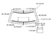
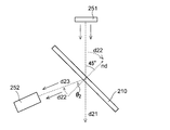
- FIG. 1 is a diagram for explaining the first to third embodiments, and is a perspective view schematically showing a moving body provided with a heat generating plate (ply plate).
- FIG. 1 schematically shows an automobile having a front window formed of a heating plate (ply plate) as an example of a moving body.
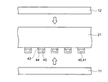
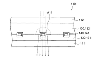
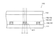
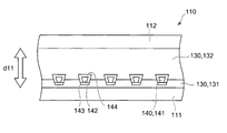
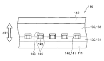
- FIG. 2 is a diagram illustrating the heat generating plates (matching plates) according to the first to third embodiments from the normal direction of the plate surfaces.
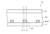
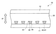
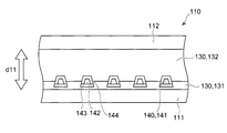
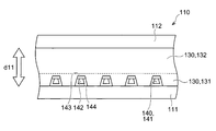
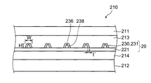
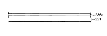
- FIG. 3 is a cross-sectional view of the heat generating plate according to the first embodiment, taken along line AA of FIG. FIG.
- FIG. 4 is a plan view showing the heating conductors of the first embodiment and the second embodiment from the normal direction of the plate surface of the heating plate, and is a plan view showing an example of the heating conductor. It is.
- FIG. 5 is a plan view showing the heat-generating conductors of the first embodiment and the second embodiment from the normal direction of the plate surface of the heat-generating plate, and shows another example of the heat-generating conductor. It is a top view.
- FIG. 6 is a diagram for explaining the operation of the heating plate of FIG.
- FIG. 7 is a diagram for explaining an example of a method of manufacturing the heating plate according to the first embodiment and the second embodiment.
- FIG. 8 is a diagram for explaining an example of a method of manufacturing the heating plate according to the first embodiment and the second embodiment.
- FIG. 9 is a diagram for explaining an example of a method of manufacturing the heating plate according to the first embodiment and the second embodiment.
- FIG. 10 is a diagram for explaining an example of a method of manufacturing the heating plate according to the first embodiment and the second embodiment.
- FIG. 11 is a diagram for explaining an example of a method of manufacturing the heating plate according to the first embodiment and the second embodiment.
- FIG. 12 is a diagram for explaining an example of a method of manufacturing the heating plate according to the first embodiment and the second embodiment.
- FIG. 13 is a diagram for explaining another example of the method of manufacturing the heat generating plates according to the first embodiment and the second embodiment.
- FIG. 14 is a diagram for explaining another example of the method for manufacturing the heating plate according to the first embodiment.
- FIG. 10 is a diagram for explaining an example of a method of manufacturing the heating plate according to the first embodiment and the second embodiment.
- FIG. 11 is a diagram for explaining an example of a method of manufacturing the heating plate according to the first embodiment and the second embodiment.
- FIG. 15 is a cross-sectional view illustrating a modification of the cross-sectional shape of the linear conductor included in the heating plate according to the first embodiment.
- FIG. 16 is a cross-sectional view showing another modification of the cross-sectional shape of the linear conductor included in the heat generating plate according to the first embodiment.
- FIG. 17 is a cross-sectional view illustrating a modified example of the linear conductor included in the heating plate according to the first embodiment.
- FIG. 18 is a diagram for explaining the operation of a conventional heat generating plate.
- FIG. 19 is an example of a cross-sectional view of the heat generating plate of the second embodiment taken along line AA of FIG. FIG.
- FIG. 20 is another example of a cross-sectional view of the heat generating plate according to the second embodiment taken along line AA of FIG.
- FIG. 21A is a diagram for explaining the operation of the heating plate of FIG. 19.
- FIG. 21B is a diagram for explaining the operation of the heat generating plate of FIG.
- FIG. 22 is a diagram illustrating an example of a method of manufacturing the heat generating plate according to the second embodiment.
- FIG. 23 is a diagram for explaining another example of the method of manufacturing the heat generating plate according to the second embodiment.
- FIG. 24 is a diagram for explaining another example of the method for manufacturing the heating plate according to the second embodiment.
- FIG. 25 is a cross-sectional view illustrating a modification of the cross-sectional shape of the linear conductor included in the heat generating plate according to the second embodiment.
- FIG. 26 is a cross-sectional view illustrating another modification of the cross-sectional shape of the linear conductor included in the heat generating plate according to the second embodiment.
- FIG. 27 is a cross-sectional view illustrating still another modification of the cross-sectional shape of the linear conductor included in the heat generating plate according to the second embodiment.
- FIG. 28 is a cross-sectional view illustrating still another modification of the cross-sectional shape of the linear conductor included in the heat generating plate according to the second embodiment.
- FIG. 26 is a cross-sectional view illustrating another modification of the cross-sectional shape of the linear conductor included in the heat generating plate according to the second embodiment.
- FIG. 27 is a cross-sectional view illustrating still another modification of the cross-sectional shape of the linear conductor included in the heat generating plate according to the second embodiment.
- FIG. 29 is a cross-sectional view illustrating a modification of the linear conductor included in the heat generating plate according to the second embodiment.
- FIG. 30 is a cross-sectional view illustrating another modified example of the linear conductor included in the heating plate according to the second embodiment.
- FIG. 31 is a diagram for explaining the operation of the conventional heat generating plate.
- FIG. 32 is a cross-sectional view of the laminated plate of the third embodiment taken along line AA of FIG.
- FIG. 33 is a plan view showing the patterned conductor of the third embodiment from the normal direction of the sheet surface, and is a plan view showing an example of the conductor.
- FIG. 34 is a plan view showing the patterned conductor of the third embodiment from the normal direction of the sheet surface, and is a plan view showing another example of the conductor.
- FIG. 35 is a diagram for describing an example of a method of manufacturing a plywood according to the third embodiment.
- FIG. 36 is a view for explaining an example of a method for manufacturing a plywood according to the third embodiment.
- FIG. 37 is a diagram for describing an example of a method for manufacturing a plywood according to the third embodiment.
- FIG. 38 is a diagram for describing an example of a method of manufacturing a plywood according to the third embodiment.
- FIG. 39 is a view illustrating an example of a method for manufacturing a laminated plate according to the third embodiment.
- FIG. 40 is a diagram for describing an example of a method for manufacturing a plywood according to the third embodiment.
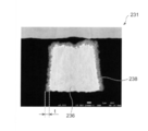
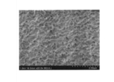
- FIG. 41 is an enlarged photograph showing a part of the linear conductor in the laminated plate according to the third embodiment.
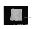
- FIG. 42 is a photograph showing one cross section of the linear conductor in the laminated plate according to the third embodiment.
- FIG. 43 is a diagram for explaining the operation of the combination plate according to the third embodiment.
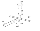
- FIG. 44 is a diagram illustrating an example of a method of measuring the luminance of light reflected by the mating plate according to the third embodiment.
- FIG. 45 is a diagram illustrating another example of a method of measuring the luminance of light reflected by the mating plate according to the third embodiment.
- FIG. 41 is an enlarged photograph showing a part of the linear conductor in the laminated plate according to the third embodiment.
- FIG. 42 is a photograph showing one cross section of the linear conductor in the laminated plate according to the third embodiment.
- FIG. 43 is a diagram for explaining the
- FIG. 46 is a graph of the example showing the relationship between the luminance measured in the state of FIG. 44 and the inclination angle of the plywood.
- FIG. 47 is a graph of a comparative example showing the relationship between the luminance measured in the state of FIG. 44 and the inclination angle of the plywood.
- FIG. 48 is an enlarged photograph showing a part of a linear conductor in an example of a conventional laminated plate.
- FIG. 49 is an enlarged photograph showing a part of a linear conductor in another example of the conventional laminated plate.
- FIG. 50 is a photograph showing one section of a linear conductor in an example of a conventional laminated plate.
- FIG. 51 is a diagram for explaining the operation of an example of a conventional laminated plate.
- the terms “plate”, “sheet”, and “film” are not distinguished from each other based only on the difference in the names.
- the “film with a conductor” is a concept including a member that can be called a plate or a sheet. Therefore, the “film with a conductor” includes a “plate with a conductor (substrate)” and a “film with a conductor”. It cannot be distinguished from a member called “sheet” only by the difference in the name.
- sheet surface refers to a target sheet-like member (plate-like member (plate-like member) when viewed as a whole and globally. Member, film-shaped member).
- FIG. 1 to FIG. 18 are diagrams for explaining the first embodiment and modifications.
- 1 is a diagram schematically showing an automobile provided with a heating plate
- FIG. 2 is a diagram of the heating plate viewed from a normal direction of the plate surface
- FIG. 3 is a diagram illustrating a cross section of the heat generating plate according to the first embodiment, taken along line -A.
- the automobile 1 as an example of the moving object has window glasses such as a front window, a rear window, and a side window.
- window glasses such as a front window, a rear window, and a side window.
- the front window 5 is constituted by the heat generating plate 10 will be described.
- the vehicle 1 has a power source 7 such as a battery.
- FIG. 2 shows the heating plate 10 viewed from the normal direction of the plate surface.
- FIG. 3 is a cross-sectional view of the heating plate 10 taken along line AA of FIG.
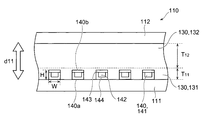
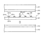
- the heating plate 10 is disposed between the first substrate 11 and the second substrate 12 that are separated from each other in the first direction d1.
- a bonding layer 30 for bonding the first substrate 11 and the second substrate 12 to each other.
- the first direction matches the thickness direction of the heating plate 10 and further matches the normal direction to the plate surface of the heating plate 10.
- the heating conductor 40 is arranged at an end of the bonding layer 30 in the first direction d1. In the examples shown in FIGS.
- FIG. 3 is a diagram showing a cross section along a direction orthogonal to a longitudinal direction of a linear conductor 41 of a heating conductor 40 described later.
- the heating plate 10 has a wiring portion 15 for supplying electricity to the heating conductor 40.
- power is supplied from the power supply 7 such as a battery to the heating conductor 40 from the wiring portion 15 through the bus bar 45 of the heating conductor 40, and the heating conductor 40 is heated by resistance heating.
- the heat generated by the heat generating conductor 40 is transmitted to the first substrate 11 and the second substrate 12, and the first substrate 11 and the second substrate 12 are warmed. Thereby, it is possible to remove the fogging due to the dew condensation attached to the first substrate 11 and the second substrate 12. If snow or ice is attached to the first substrate 11 and the second substrate 12, the snow and ice can be melted. Therefore, the occupant's field of view is well secured.
- a switch is usually inserted (connected in series) between the power supply 7 and the bus bar 45 of the heating conductor 40 in the wiring section 15. Then, only when the heating plate 10 needs to be heated, the switch is closed to energize the heating conductor 40.
- the first substrate 11 and the second substrate 12 will be described.
- a substrate having a high visible light transmittance so as not to obstruct the occupant's view.
- the material of the first substrate 11 and the second substrate 12 include soda lime glass and blue plate glass.
- the visible light transmittance of the first substrate 11 and the second substrate 12 is preferably 90% or more.
- the visible light transmittance of the first substrate 11 and the second substrate 12 is measured at a wavelength of 380 nm to 780 nm using a spectrophotometer (“UV-3100PC” manufactured by Shimadzu Corp., conforming to JIS K-0115).
- the visible light transmittance of this part may be reduced by coloring a part or the whole of the first substrate 11 and the second substrate 12. In this case, it is possible to block direct sunlight and make it difficult to visually recognize the inside of the vehicle from outside.
- the first substrate 11 and the second substrate 12 have a thickness of 1 mm or more and 5 mm or less. With such a thickness, the first substrate 11 and the second substrate 12 having excellent strength and optical characteristics can be obtained.
- the first substrate 11 and the second substrate 12 may be made of the same material and have the same configuration, or may be different from each other in at least one of the material and the configuration.
- the bonding layer 30 is disposed between the first substrate 11 and the second substrate 12, and bonds the first substrate 11 and the second substrate 12.
- layers made of various adhesive or tacky materials can be used. Further, it is preferable to use a material having a high visible light transmittance for the bonding layer 30.
- a layer made of polyvinyl butyral (PVB) can be exemplified.
- the bonding layer 30 has a first portion 31 and a second portion 32. The first portion 31 is adjacent to the heating conductor 40. The second portion 32 is located offset from the first portion 31 in the first direction d1. The first portion 31 is in contact with the first substrate 11, and the second portion 32 is in contact with the second substrate 12.
- the thickness of the bonding layer 30, that is, the length in the first direction d1, is, for example, not less than 20 ⁇ m and not more than 1000 ⁇ m. If the bonding layer 30 has a sufficient thickness, when the heat generating plate 10 is damaged, it is possible to prevent the fragments and the like of the first substrate 11 from being scattered. This is preferable because it can suppress the penetration of the heat generating plate 10.
- the thickness T1 of the first portion 31, that is, the length in the first direction d1, is shorter than the thickness T2 of the second portion, that is, the length in the first direction d1.
- the thickness T1 of the first portion 31 can be set to 20 ⁇ m or more and 100 ⁇ m or less, and can be set to 40 ⁇ m or more and 80 ⁇ m or less.
- the thickness T2 of the second portion 32 can be, for example, not less than 150 ⁇ m and not more than 1600 ⁇ m.
- the heating plate 10 is not limited to the illustrated example, and may be provided with another functional layer expected to exhibit a specific function. Further, one functional layer may exhibit two or more functions. For example, some function may be given to at least one of the first substrate 11 and the second substrate 12 of the heating plate 10 and the bonding layer 30. Examples of the functions that can be provided to the heating plate 10 include an anti-reflection (AR) function, a hard coat (HC) function having scratch resistance, an infrared shielding (reflection) function, an ultraviolet shielding (reflection) function, and an antifouling property. Functions and the like can be exemplified.
- FIGS. 4 and 5 are plan views of the heat-generating conductor 40 viewed from the normal direction of the plate surface of the heat-generating plate 10.
- FIG. 4 shows an example of an arrangement pattern of the linear conductors 41 forming the heating conductor 40
- FIG. 5 shows another arrangement pattern of the linear conductors 41 forming the heating conductor 40. An example is shown.
- the heating conductor 40 has a pair of bus bars 45 and a plurality of linear conductors 41 disposed between the pair of bus bars 45.
- the pair of bus bars 45 are arranged apart from each other in the second direction d2, and each is electrically connected to the corresponding wiring portion 15.
- the second direction d2 is a direction along the plate surface of the heat generating plate 10, and in the illustrated example, is orthogonal or substantially orthogonal to the first direction d1.
- the voltage of the power supply 7 connected to the wiring section 15 is applied between the pair of bus bars 45.
- the linear conductor 41 is connected to a pair of bus bars 45 at both ends. Therefore, the linear conductor 41 electrically connects the pair of bus bars 45.
- the linear conductor 41 When a voltage is applied through the wiring portion 15 and the bus bar 45, the linear conductor 41 generates heat by resistance heating. Then, the heat is transmitted to the first substrate 11 and the second substrate 12 via the bonding layer 30, so that the first substrate 11 and the second substrate 12 are warmed.
- the sheet resistance of the heat generating conductor 40 in accordance with the applied voltage.
- the applied voltage is about 12 V
- it is preferably 0.1 ⁇ / ⁇ or more and 1 ⁇ / ⁇ or less
- the applied voltage is about 48 V
- it is preferably 1 ⁇ / ⁇ or more and 13 ⁇ / ⁇ or less. Therefore, when the applied voltage is in the range of 12 to 48 V, the sheet resistance is preferably from 0.1 ⁇ / ⁇ to 13 ⁇ / ⁇ .
- the resistance of the heat generating conductor 40 is too large, the amount of heat generated by the heat generating conductor 40 is insufficient, and the first substrate 11 and the second substrate 12 cannot be appropriately heated. If the resistance of the heating conductor 40 is too small, the amount of heat generated in the heating conductor 40 becomes too large, and uneven heating is likely to occur between the area near the linear conductor 41 and other areas. Become.
- the heating conductors 40 can be arranged in various patterns.
- the heating conductor 40 is formed by arranging the linear conductors 41 in a mesh pattern defining a plurality of opening regions 47.
- the heating conductor 40 includes a plurality of connecting elements 48 extending between two branch points 46 and defining an open area 47. That is, the linear conductor 41 of the heating conductor 40 is configured as a group of a plurality of connection elements 48 forming the branch points 46 at both ends.
- the mesh-shaped pattern may be an irregular mesh pattern in which the shape and size of each of the opening regions 47 are not congruent and have no constant repetition period in a plane. And the size may be the same, and the opening region 47 may be a periodic lattice mesh pattern having a constant repetition period in a plane.
- the average distance between the centers of gravity of the opening regions 47 is preferably 10,000 ⁇ m or less, more preferably 7000 ⁇ m or less, and even more preferably 5000 ⁇ m or less. If the distance between the centers of gravity of the two adjacent opening regions 47 is too small, the transmittance is deteriorated and the transparency is impaired. Therefore, the average distance between the centers of gravity of the opening regions 47 is preferably 100 ⁇ m or more. .
- the heating conductor 40 includes a plurality of linear conductors 41 connecting a pair of bus bars 45 in a striped pattern. It may be formed by being arranged in. More specifically, the plurality of linear conductors 41 may be arranged with a gap 49 in a direction not parallel to the second direction d2 while extending in the second direction d2.
- the size of the gap 49 in other words, the second direction which is the arrangement direction of the gap 49.
- d2 is an average length along a non-parallel direction, in other words, an average distance between adjacent linear conductors 41 is preferably 12000 ⁇ m or less, and preferably 7000 ⁇ m or less. Is more preferable, and it is still more preferable that it is 3000 ⁇ m or less.
- the gap 49 is too small, the transmittance is deteriorated and the transparency is impaired, so that the average distance between the adjacent linear conductors 41 is preferably 100 ⁇ m or more.
- the heat generating conductor 40 is embedded in the bonding layer 30.
- the heating conductor 40 is disposed at an end of the bonding layer 30 in the first direction d1 while being embedded in the bonding layer 30. That is, the heating conductor 40 is adjacent to the bonding layer 30.
- the heating conductor 40 is in contact with the first substrate 11.
- the linear conductor 41 of the heating conductor 40 has a surface 40 a that is in contact with the first substrate 11.
- the surface roughness Sz of the surface 40a of the heat generating conductor 40 on the side in contact with the first substrate 11 is preferably 3.0 ⁇ m or less, more preferably 2.0 ⁇ m or less, and more preferably 1.0 ⁇ m or less. It is more preferred that:
- the surface roughness Sz of the surface 40b on the side adjacent to the bonding layer 30 of the heat generating conductor 40 is preferably greater than 1.0 ⁇ m, and more preferably 3.0 ⁇ m or more. Is more preferred.
- the surface roughness Sz means Sz defined by ISO25178.
- linear conductor 41 and a bus bar 45 for example, gold, silver, copper, platinum, aluminum, chromium, molybdenum, nickel, titanium, palladium, indium, tungsten, and these One or more of the alloys can be exemplified.
- the linear conductor 41 and the bus bar 45 may be formed using the same material, or may be formed using different materials.
- the linear conductor 41 can be formed using an opaque metal material as described above.
- the ratio of the region not covered by the linear conductor 41 that is, the non-coverage ratio (opening ratio) is as high as about 70% to 99%.
- the line width of the linear conductor 41 is 2 ⁇ m or more and 20 ⁇ m or less. For this reason, the region where the linear conductor 41 is provided is transparently grasped as a whole, so that the presence of the linear conductor 41 does not impair the transparency of the heating plate 10.
- the linear conductor 41 has a rectangular cross section as a whole.
- the width W of the linear conductor 41 that is, the width W along the plate surface of the heating plate 10 is 2 ⁇ m or more and 20 ⁇ m or less
- the height (thickness) H that is, the plate surface of the heating plate 10 It is preferable that the height (thickness) H along the normal line direction be 1 ⁇ m or more and 30 ⁇ m or less. According to the linear conductor 41 having such dimensions, since the linear conductor 41 is sufficiently thinned, the linear conductor 41 can be effectively made invisible.
- the ratio (H / W) of the height H to the line width W of the linear conductor 41 is preferably 0.5 or more and 1.8 or less. It is more preferably 7 or more and 1.5 or less, further preferably 0.9 or more and 1.35 or less.
- the linear conductor 41 having such a dimensional ratio is easy to manufacture, and can be configured such that the width is too large with respect to the height and does not impair the transparency. Further, even if the linear conductor 41 having such a dimensional ratio is observed from a direction inclined in the normal direction of the heating plate 10, the width of the visible linear conductor 41 hardly changes. In other words, seeing from a direction inclined in the normal direction of the heating plate 10 does not easily impair the transparency.
- the ratio (T1 / H) of the thickness T1 of the first portion 31 of the bonding layer 30 to the height H of the linear conductor 41 is preferably 3 or more and 8 or less, and more preferably 4 or more and 7 or less. Is more preferred.
- the ratio (T2 / H) of the thickness T2 of the second portion 32 of the bonding layer 30 to the height H of the linear conductor 41 is preferably 20 or more and 130 or less, and is 60 or more and 110 or less. Is more preferred. In such a case, when the heat generating conductor 40 is embedded in the first portion 31 (the base film 21) of the bonding layer 30 in the manufacturing process of the heat generating plate 10 described later, it is possible to effectively suppress the entry of air and the like. can do.
- the linear conductor 41 is formed of a conductive layer 42, a second dark layer 44 that covers the side of the surface of the conductive layer 42 that faces the first substrate 11 and both sides.
- a first dark color layer 43 that covers the surface of the conductive layer 42 on the side facing the second substrate 12 may be included.
- the linear conductor 41 includes at least a dark layer covering the surface of the second dark layer 44 on the side facing the first substrate 11.
- the conductive layer 42 made of a metal material having excellent conductivity exhibits a relatively high reflectance. When light is reflected by the conductive layer 42 forming the linear conductor 41, the reflected light becomes visible, which may obstruct the occupant's view.
- the first dark layer 43 and the second dark layer 44 cover at least a part of the surface of the conductive layer 42.
- the first dark color layer 43 and the second dark color layer 44 may be layers having a lower visible light reflectance than the conductive layer 42, and are dark layers such as black.
- the first dark color layer 43 and the second dark color layer 44 have a visible light reflectance of 15% or less, preferably 8% or less, more preferably 5% or less.
- the first dark color layer 43 and the second dark color layer 44 make it difficult for the conductive layer 42 to be visually recognized, so that the occupant's view can be secured well.
- the surface of the surface 40b of the heat generating conductor 40 adjacent to the bonding layer 30 is rough, the first dark color formed on the side surface of the conductive layer 42 formed on the surface of the linear conductor 41 The layer 43 and the second dark layer 44 are roughened.
- a heating conductor made of a tungsten wire is disposed between two substrates while being supported by a heat-sealing transparent substrate film, and is bonded. It was bonded to each substrate by layers.
- a heating wire (wire) formed of such tungsten has a relatively high volume resistivity.
- the thin heating wire is easily broken, it is also difficult to process the heating plate with high yield. For these reasons, the heating wire made of tungsten is formed thick. For this reason, the heating wire included in the heating plate is easily recognized, and the visibility of the field of view through the heating plate is deteriorated.
- a heating conductor made of a heating wire made of copper or the like and having a line width of 10 ⁇ m or less was supported on a transparent substrate made of polyethylene terephthalate (PET) or the like. In this state, it was arranged between the two bonding layers and bonded to each substrate by the bonding layers. Therefore, the heat generating conductor is hard to be visually recognized, and it is effective in obtaining good transparency.
- a voltage is applied to the heating conductor to cause the heating plate to generate heat, distortion may occur in the field of view through the heating plate. The distortion can deteriorate visibility through the heating plate.
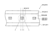
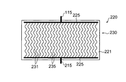
- the resin layer 530 is a layer including a bonding layer and a transparent base material.
- the refractive index of the resin layer 530 is more likely to change due to a temperature rise than the substrates 511 and 512 made of glass or the like.
- the present inventors have also confirmed that the occurrence of the difference in the refractive index in the resin layer 530 is caused by uneven temperature in the resin layer 530.
- the peripheral region A2 near each linear conductor 541 of the heating conductor 540 becomes , More susceptible to heat than other areas.
- the peripheral area A2 of the linear conductor 541 is warmed more than other areas. That is, temperature unevenness occurs between the peripheral region A2 and other regions.
- the resin layer 530 is deteriorated by heat. Due to the alteration, the refractive index of the resin layer 530 in the peripheral region A2 changes.
- a difference in the refractive index occurs between the peripheral region A2 of the resin layer 530 and the region other than the peripheral region A2.
- light transmitted between the peripheral region A2 and the region other than the peripheral region A2 is refracted as shown by a solid arrow in FIG.
- the light incident on the heat generating plate 510 passes through the heat generating plate 510 in a state where heat is generated, the light spreads far more than the dotted arrow indicating light that is not refracted and is emitted.
- the emitted light spreads more as the area A2 in which the resin layer 530 deteriorates becomes larger.
- the distortion occurs in the field of view via the heating plate 510.
- the heat generating conductor 40 has a surface 40 a in contact with the first substrate 11.
- the heat generated by the heat generating conductor 40 can be efficiently transmitted to the first substrate 11.
- the first substrate 11 made of glass or the like is more likely to conduct heat than the bonding layer 30 made of resin or the like. That is, more heat is conducted to the first substrate 11. In other words, the heat conducted to the bonding layer 30 is reduced. For this reason, the peripheral region A1 where deterioration due to heat can occur can be reduced. Since the light incident on the heating plate 10 is less likely to spread, generation of distortion can be suppressed. Further, since heat is easily transmitted to the first substrate 11, the first substrate 11 can efficiently generate heat. This is particularly effective when it is desired to efficiently generate heat only on one side of the heat generating plate 10, such as the outside of the front window 5 of the automobile 1 shown in FIG.
- the surface roughness Sz of the surface 40a of the heating conductor 40 on the side in contact with the first substrate 11 is preferably 3.0 ⁇ m or less, more preferably 2.0 ⁇ m or less, and further preferably 1.0 ⁇ m or less. It is as follows. That is, the portion where the heating conductor 40 and the first substrate 11 are in contact with each other is large. In this case, the heat generated by the heating conductor 40 can be efficiently transmitted to the first substrate 11. That is, more heat is conducted to the first substrate 11. In other words, the heat conducted to the bonding layer 30 is reduced. For this reason, the peripheral region A1 where deterioration due to heat can occur can be made smaller.
- the first substrate 11 can efficiently generate heat. This is particularly effective when only one side of the heat generating plate 10 such as the outside of the front window 5 of the automobile 1 shown in FIG.
- the surface roughness Sz of the surface 40b of the heat generating conductor 40 on the side adjacent to the bonding layer 30 is preferably larger than 1.0 ⁇ m, and more preferably 3.0 ⁇ m or more. In other words, it is preferable that a portion where the heat generating conductor 40 and the bonding layer 30 are in contact is small. In this case, the heat generated in the heating conductor 40 is not easily transmitted to the bonding layer 30 by heat conduction. For this reason, the peripheral region A1 where deterioration due to heat can occur can be made smaller. Since the light incident on the heating plate 10 is less likely to spread, the occurrence of distortion can be further suppressed.
- the heat generated in the heating conductor 40 is easily transmitted by radiation (radiation). According to the transmission of heat by radiation, local heating of the heat generating plate 10 can be avoided, and more uniform heating can be realized than the transmission by heat conduction. For this reason, the peripheral region A1 where deterioration due to heat can occur can be made smaller. Since the light incident on the heating plate 10 is less likely to spread, the occurrence of distortion can be further suppressed. Moreover, according to the transfer of heat by radiation, the first substrate 11 and the second substrate 12 can be efficiently heated, or snow, water droplets, and the like attached to the surface of the heating plate 10 can be directly heated. That is, the function of the heat generating plate 10 can be exhibited more efficiently.
- the linear conductor 41 preferably includes a first dark color layer 43 or a second dark color layer 44 provided on at least a part of the surface.
- the linear conductor 41 preferably includes the second dark layer 44 provided on the side facing the first substrate 11.
- the first substrate 11 and the second substrate 12 can be efficiently heated, or snow, water droplets, etc. attached to the surface of the heating plate 10 can be directly heated. That is, the function of the heat generating plate 10 can be exhibited more efficiently.
- the distance between the centers of gravity of two adjacent opening regions 47 is 100 ⁇ m or more and 10000 ⁇ m or less, more preferably 7000 ⁇ m or less, and further preferably 5000 ⁇ m or less.
- the average length of the gap 49 along a direction not parallel to the second direction d2 is 100 ⁇ m or more and 12000 ⁇ m or less, and more preferably 7000 ⁇ m or less. And more preferably 3,000 ⁇ m or less.
- the peripheral region A1 where deterioration due to heat can occur can be made smaller. Since the light incident on the heating plate 10 is less likely to spread, the occurrence of distortion can be further suppressed.
- the sheet resistance of the heat generating conductor 40 is 0.1 ⁇ / ⁇ or more and 1 ⁇ / ⁇ or less, more preferably 0.2 ⁇ / ⁇ or more, and further preferably 0.3 ⁇ / ⁇ or more. It has become.
- the heat generation amount is too large, so that the heat generation unevenness occurs between the area near the linear conductor 41 and other areas. This can be suppressed. For this reason, the peripheral region A1 where deterioration due to heat can occur can be made smaller. Since the light incident on the heating plate 10 is less likely to spread, the occurrence of distortion can be further suppressed.
- the ratio (T1 / H) of the thickness T1 of the first portion 31 of the bonding layer 30 to the height H of the linear conductor 41 is preferably 3 or more, and more preferably 4 or more.
- the heating conductor 40 in the manufacturing process of the heating plate 10 causes the first portion 31 of the bonding layer 30 (the base film 31).
- the heat generating conductor 40 is easily and completely embedded in the first portion 31. In other words, the heat generating conductor 40 is embedded in the first portion 31 without any gap. Therefore, entry of air or the like between the first substrate 11 and the bonding layer 30 can be effectively suppressed.
- the ratio (T2 / H) of the thickness T2 of the second portion 32 of the bonding layer 30 to the height H of the linear conductor 41 is preferably 20 or more, and more preferably 60 or more.
- the heating conductor 40 in the manufacturing process of the heating plate 10 causes the first portion 31 of the bonding layer 30 (the base film 31).
- the deformation of the first portion 31 caused by the heating conductor 40 being embedded in the first portion 31 can be easily flattened by the second portion 32. In other words, it is possible to prevent a gap from being generated between the first portion 31 and the second portion 32. Therefore, it is possible to effectively suppress air or the like from entering between the first portion 31 and the second portion 32 or between the second portion 32 and the second substrate 12.
- the ratio (T1 / H) of the thickness T1 of the first portion 31 of the bonding layer 30 to the height H of the linear conductor 41 is set so that the entire thickness of the heating plate 10 is not excessively large. , 8 or less, and more preferably 7 or less.
- the ratio (T2 / H) of the thickness T2 of the second portion 32 of the bonding layer 30 to the height H of the linear conductor 41 is preferably 130 or less, and more preferably 110 or less. More preferred.
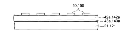
- a dark film 43a for forming the first dark layer 43 is provided on the base film 21 for forming a part of the bonding layer 30.
- the base film 21 has a heat sealing property.
- the dark color film 43a is provided in a state where it is processed to be coarse.
- the dark color film 43a is processed so as to be rough.
- the dark-colored film 43a can be treated so as to be coarse by, for example, immersing it in a mixture of an aqueous solution of sodium chlorite and an aqueous solution of sodium hydroxide. That is, the surface has a large surface roughness Sz.
- a conductive film 42a for forming the conductive layer 42 is provided on the dark film 43a.
- the conductive film 42a can be formed by a known method. For example, a method of attaching a metal foil such as a copper foil, a plating method including electroplating and electroless plating, a sputtering method, a CVD method, a PVD method, an ion plating method, or a method combining two or more of these methods is employed. can do.
- the conductive film 42a may be formed by applying a paste-like material containing a conductive metal or the like.
- two layers may be formed at the same time by sticking an electrolytic copper foil or a rolled copper foil composed of the conductive film 42a having the dark color film 43a that has been processed to be coarse.
- a resist pattern 50 is provided on the conductive film 42a.
- the resist pattern 50 has a shape corresponding to the arrangement pattern of the linear conductors 41 to be formed.
- This resist pattern 50 can be formed by patterning using a known photolithography technique.
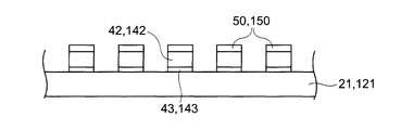
- the conductive film 42a and the dark color film 43a are etched using the resist pattern 50 as a mask. By this etching, the conductive film 42a and the dark color film 43a are patterned into a pattern substantially the same as the resist pattern 50. As a result, as shown in FIG. 9, a conductive layer 42 which forms a part of the linear conductor 41 is formed from the patterned conductive film 42a. In addition, a first dark layer 43 that forms a part of the linear conductor 41 is formed from the patterned dark film 43a.
- the etching method is not limited to wet etching using an etching solution, and a known method can be employed. As a known method, for example, plasma etching may be used. After the etching step, the resist pattern 50 is removed as shown in FIG.
- a second dark layer 44 is formed on the surface and the side of the conductive layer 42 opposite to the surface on which the first dark layer 43 is provided.
- the second dark layer 44 is formed, for example, by performing a darkening process (blackening process) on a part of the material forming the conductive layer 42, and forming a second layer made of metal oxide or metal sulfide from the part forming the conductive layer 42.
- a dark layer 44 can be formed.
- the second dark color layer 44 may be provided on the surface of the conductive layer 42.
- the surface of the conductive layer 42 may be roughened to provide the second dark layer 44.
- the conductor-attached film 20 including the heat-generating conductor 40 and the base film 21 supporting the heat-generating conductor 40 is manufactured.
- the bus bar 45 of the heating conductor 40 may be formed integrally with the conductive layer 42 of the linear conductor 41 by patterning the conductive film 42a, or may be a line provided on the base film 21.
- the conductor 41 may be separate from the conductor 41.
- the heating conductor 40 supported by the base film 21 is disposed between the first substrate 11 and the second substrate 12.
- an adhesive film 22 is disposed between the first substrate 11 and the second substrate 12 and on the side of the base film 21 of the film with conductor 20.
- the adhesive film 22 has a heat sealing property.
- the first substrate 11 and the second substrate 12 are joined by pressing and heating toward each other.
- the heating conductor 40 is embedded in the base film 21 while being in contact with the first substrate 11.
- the base film 21 and the adhesive film 22 are heated and pressed, the base film 21 becomes the first portion 31 of the bonding layer 30, and the bonding film 22 becomes the second portion 32 of the bonding layer 30.
- the bonding layer 30 is formed by the base film 21 and the adhesive film 22.
- the bonding layer 30 may be formed only from the base film 21 by making the base film 21 on which the dark film 43a and the conductive film 42a are provided with a sufficient thickness.
- the heating conductor 40 supported by the base film 21 is disposed between the first substrate 11 and the second substrate 12, and the first substrate 11 and the second substrate 12 are Press and heat toward each other to join.
- the heating conductor 40 is embedded in the base film 21 while being in contact with the first substrate 11.
- the side of the base film 21 on which the heating conductor 40 is provided is from the side opposite to the side of the base film 21 on which the heating conductor 40 is provided to support the heating conductor 40. , So that the hardness is high.
- the side of the heat generating conductor 40 of the base film 21 having the higher hardness becomes the first portion 31 of the bonding layer 30 and is separated from the heat generating conductor 40 of the base film 21 having the lower hardness.
- the side becomes the second portion 32 of the bonding layer 30.
- the heating plate 10 shown in FIG. 3 is also manufactured in such a process.
- the heat generating plate 10 is provided between the first substrate 11 and the second substrate 12 that are spaced apart from each other in the first direction d1.
- the heat generating conductor 40 includes a heating conductor 40 that is disposed and generates heat when a voltage is applied thereto, and a bonding layer 30 that bonds the first substrate 11 and the second substrate 12 together.
- the heating conductor 40 has a surface in contact with the first substrate 11. According to such a heating plate 10, heat generated by the heating conductor 40 can be efficiently transmitted to the first substrate 11. In other words, the heat conducted to the bonding layer 30 is reduced. For this reason, the peripheral region A1 where deterioration due to heat can occur can be reduced. Therefore, it is possible to suppress the occurrence of distortion in the field of view via the heating plate 10 while the heating plate 10 is generating heat.
- the surface roughness Sz of the heat generating conductor 40 on the side in contact with the first substrate 11 is 3.0 ⁇ m or less. According to such a heating plate 10, heat generated by the heating conductor 40 can be efficiently transmitted to the first substrate 11. For this reason, more heat is conducted to the first substrate 11, and the peripheral region A1 where deterioration due to heat may occur can be made smaller. Therefore, since the light incident on the heat generating plate 10 is hardly spread, the occurrence of distortion can be further suppressed.
- the method of manufacturing the heat generating plate 10 according to the first embodiment includes a step of providing the conductive film 42a on the base film 21 having heat sealing properties, a step of patterning the conductive film 42a, and a step of forming the first substrate 11 and A step of pressing and heating the first substrate 11 and the second substrate 12 toward each other in a state where the base film 21 is disposed between the second substrates 12 and joining them.
- the method for manufacturing the heating plate 10 since the conductive film 42 a that forms the conductive layer 42 is formed on the base film 21 having heat sealing properties, the above-described heating plate 10 can be easily manufactured. Can be.
- the heat generating plate 10 is formed in a curved shape.
- the present invention is not limited to this example, and the heat generating plate 10 may be formed in a flat shape.
- the linear conductor 41 has a rectangular cross section. That is, in the cross section of the linear conductor 41, opposing sides in the first direction d1 are parallel and have the same length.
- the linear conductor 41 is not limited to a rectangular shape, and may have, for example, a trapezoidal cross section. Further, the linear conductor 41 may have different lengths on opposite sides facing the first direction d1.
- the cross-sectional shape of the linear conductor 41 may be a trapezoidal shape in which the side in contact with the first substrate 11 is the shorter side of the two opposite sides parallel to each other.
- the linear conductor 41 may have different widths on opposite sides in a cross section along the first direction d1.
- the width of the linear conductor 41 in a direction orthogonal to the first direction d1 may be narrower at a position closest to the second substrate 12 than at a position in contact with the first substrate 11.
- the width of the linear conductor 41 along a direction orthogonal to the first direction d1 may be gradually reduced from the first substrate 11 side to the second substrate 12 side.
- the legs in the cross section of the linear conductor 41 that is, the side surfaces of the linear conductor 41 may be inclined toward a direction orthogonal to the first direction and face the second substrate 12. it can. For this reason, the heat transmitted by the radiation from the side surface of the linear conductor 41 tends to travel to the second substrate 12. That is, not only the first substrate 11 but also the second substrate 12 can be appropriately heated.
- the side surface of the linear conductor 41 is not limited to a straight line as in the example shown in FIG. 15 in a cross section along the first direction d1, but may be curved.
- the surface roughness Sz of the side surface of the linear conductor 41 is larger than 1.0 ⁇ m, local heating of the heating plate 10 is avoided by radiation from the side surface of the linear conductor 41 to make the heating plate 10 uniform.
- the heat can be transferred to the second substrate 12 while being heated.
- the second substrate 12 can efficiently generate heat.
- the side surface of the linear conductor 41 includes the second dark layer 44, radiation from the side surface of the linear conductor 41 can be promoted. It is possible to efficiently transfer heat to the second substrate 12 while uniformly heating the heating plate 10 by effectively avoiding local heating of the heating plate 10 by radiation from the side surface of the linear conductor 41. it can. In other words, the second substrate 12 can generate heat more efficiently.
- the heating conductor 40 supported by the base film 21 in a state where the heating conductor 40 supported by the base film 21 is disposed between the first substrate 11 and the second substrate 12, the first substrate 11 and the second In the step of pressing and heating the two substrates 12 toward each other and joining them, the legs in the cross section of the linear conductor 41, that is, the side surfaces of the linear conductor 41 are inclined with respect to a direction orthogonal to the first direction d1.
- the heating conductor 40 is embedded in the base film 21 when facing the side of the second substrate 12, air flows between the first substrate 11 and the base film 21 and the heating conductor 40. And the like can be effectively suppressed. Therefore, it is possible to prevent the visibility through the heating plate 10 from being deteriorated by the bubbles.
- the cross-sectional shape of the linear conductor 41 may be a trapezoidal shape in which the side in contact with the first substrate 11 is the longer side of the two opposite sides that are parallel.
- the width of the linear conductor 41 in a direction orthogonal to the first direction d1 may be wider at a position closest to the second substrate 12 than at a position in contact with the first substrate 11.
- the width of the linear conductor 41 along a direction orthogonal to the first direction d1 may be gradually increased from the first substrate 11 side to the second substrate 12 side.
- the legs in the cross section of the linear conductor 41 that is, the side surfaces of the linear conductor 41 may be inclined with respect to a direction orthogonal to the first direction d1 and face the first substrate 11 side. it can. For this reason, the heat transmitted by the radiation from the side surface of the linear conductor 41 tends to travel to the first substrate 11. That is, the first substrate 11 can be efficiently heated.
- the side surface of the linear conductor 41 is not limited to a straight line as in the example shown in FIG. 15 in a cross section along the first direction d1, but may be curved.
- the surface roughness Sz of the side surface of the linear conductor 41 is greater than 1.0 ⁇ m, local heating of the heating plate 10 is avoided by radiation from the side surface of the linear conductor 41 to make the heating plate 10 uniform.
- the heat can be efficiently transmitted to the first substrate 11 while being heated.
- the entire first substrate 11 can be efficiently heated.
- the side surface of the linear conductor 41 includes the second dark layer 44, radiation from the side surface of the linear conductor 41 can be promoted. Radiation from the side surface of the linear conductor 41 effectively avoids local heating of the heating plate 10 and efficiently transfers heat to the first substrate 11 while uniformly heating the heating plate 10. it can. In other words, the entire first substrate 11 can be more efficiently heated.
- the linear conductor 41 having such a tapered cross-sectional shape is formed by, for example, making the dark-colored film 43a forming the first dark-colored layer 43 more difficult to be etched than the conductive film 42a forming the conductive layer 42.
- it can be formed by being easily etched. That is, if the dark color film 43a is less likely to be etched than the conductive film 42a, the dissolution of the dark color film 43a is less likely to progress than the conductive film 42a, and the etching of the conductive film 42a on the side of the dark color film 43a is less likely to progress. Therefore, as shown in FIG.
- the cross-sectional shape of the linear conductor 41 is tapered toward the side in contact with the first substrate 11, typically, the cross-sectional shape of the linear conductor 41 is the first shape.
- the side in contact with the substrate 11 has a trapezoidal shape that is the shorter side of the two opposite sides that are parallel (substantially parallel). If the dark film 43a is more easily etched than the conductive film 42a, the dissolution of the dark film 43a proceeds from the conductive film 42a, and the conductive film 42a is also etched from the side of the dissolved dark film 43a. Therefore, as shown in FIG.
- the cross-sectional shape of the linear conductor 41 has a tapered shape tapered toward the side in contact with the first substrate 11, and typically, the side in contact with the first substrate 11 is parallel ( It has a trapezoidal shape that is the shorter side of the two opposite sides (substantially parallel).
- the second dark layer 44 may be provided as follows. First, after the conductive film 42a and the dark color film 43a are patterned into substantially the same pattern as the resist pattern 50 by an etching process, the second dark color layer roughened on the side surface of the conductive layer 42 without removing the resist pattern 50. 44 is formed. Thereafter, the resist pattern 50 is removed, and another part of the second dark color layer 44 that is not roughened is formed on the surface of the conductive layer 42 opposite to the surface on which the first dark color layer 43 is provided.
- the surface roughness Sz of the heating conductor 40 on the side in contact with the first substrate 11 can be easily reduced. That is, the surface roughness Sz of the heat generating conductor 40 on the side in contact with the first substrate 11 can be easily reduced to 3.0 ⁇ m or less.
- the second dark layer 44 may not be provided on the side in contact with the first substrate 11. That is, the second dark layer 44 may be provided only on the side surface of the conductive layer 42.
- Such a second dark layer 44 is formed on the side surface of the conductive layer 42 without removing the resist pattern 50 after the conductive film 42a and the dark film 43a are patterned into substantially the same pattern as the resist pattern 50 by an etching process. It can be provided by forming a part of the roughened second dark layer 44.
- the conductive layer 42 is exposed on the side in contact with the first substrate 11.
- the conductive layer 42 has a small surface roughness. Therefore, the surface roughness Sz of the heat generating conductor 40 on the side in contact with the first substrate 11 can be easily reduced. That is, the surface roughness Sz of the heat generating conductor 40 on the side in contact with the first substrate 11 can be easily reduced to 3.0 ⁇ m or less.
- FIGS. 1, 2, 4, 5, 7 to 13, and 18 to 31 are diagrams for explaining the second embodiment and modifications.
- 1 is a diagram schematically showing an automobile provided with a heating plate
- FIG. 2 is a diagram of the heating plate viewed from a normal direction of the plate surface
- FIGS. 19 and 20 are diagrams of FIG. It is a figure showing an example of a section of a heat generating plate concerning a 2nd embodiment along another AA line of Drawing 2, and another example.
- the automobile 101 as an example of the moving object has window glasses such as a front window, a rear window, and a side window.
- window glasses such as a front window, a rear window, and a side window.
- the front window 105 is constituted by the heat generating plate 110 is illustrated.
- the automobile 101 has a power supply 107 such as a battery.
- FIG. 2 shows the heating plate 110 viewed from the normal direction of the plate surface.
- FIGS. 19 and 20 are cross-sectional views of the heat generating plate 110 shown in FIG. 2 taken along the line AA.
- the heating plate 110 is formed by the first substrate 111 and the second substrate 112 that are separated from each other in the first direction d11 and the first substrate 111 and the second substrate 112. It has a heat-generating conductor 140 disposed therebetween and a bonding layer 130 for bonding the first substrate 111 and the second substrate 112.
- the first direction d11 matches the thickness direction of the heating plate 110, and further matches the normal direction to the plate surface of the heating plate 110.
- FIG. 19 and 20 are cross-sectional views of the heat generating plate 110 shown in FIG. 2 taken along the line AA.
- the heating plate 110 is formed by the first substrate 111 and the second substrate 112 that are separated from each other in the first direction d11 and the first substrate 111 and the second substrate 112. It has a heat-generating conductor 140
- the heat generating conductor 140 is disposed at an intermediate portion of the bonding layer 130 in the first direction d11.
- the heat generating conductor 140 is disposed at an end of the bonding layer 130 in the first direction d11.
- the heating plate 110 is curved, but in other drawings, the heating plate 110, the first substrate 111, The second substrate 112 is illustrated as a flat plate.
- FIGS. 19 and 20 are views showing a cross section along a direction orthogonal to the longitudinal direction of the linear conductor 141 of the heat generating conductor 140 described later.
- the heating plate 110 has a wiring portion 115 for supplying electricity to the heating conductor 140.
- the power supply 107 such as a battery supplies electricity to the heating conductor 140 from the wiring section 115 via the bus bar 145 of the heating conductor 140, and causes the heating conductor 140 to generate heat by resistance heating.
- the heat generated by the heat generating conductor 140 is transmitted to the first substrate 111 and the second substrate 112, and the first substrate 111 and the second substrate 112 are heated. Accordingly, it is possible to remove the fogging due to the dew attached to the first substrate 111 and the second substrate 112. When snow or ice is attached to the first substrate 111 and the second substrate 112, the snow or ice can be melted.
- a switch is usually inserted (connected in series) between the power supply 107 and the bus bar 145 of the heating conductor 140 in the wiring section 115. Then, only when the heating plate 110 needs to be heated, the switch is closed to energize the heating conductor 140.
- the first substrate 111 and the second substrate 112 will be described.
- the first substrate 111 and the second substrate 112 are used for a front window of an automobile as in the example shown in FIG.
- the first substrate 111 and the second substrate 112 preferably have a visible light transmittance of 90% or more.
- the material of the first substrate 111 and the second substrate 112 include soda lime glass and blue plate glass.
- the visible light transmittance of a part of the first substrate 111 and the second substrate 112 may be reduced by coloring a part or the whole of the first substrate 111 and the second substrate 112. In this case, it is possible to block direct sunlight and make it difficult to visually recognize the inside of the vehicle from outside.
- the first substrate 111 and the second substrate 112 have a thickness of 1 mm or more and 5 mm or less. With such a thickness, the first substrate 111 and the second substrate 112 having excellent strength and optical characteristics can be obtained.
- the first substrate 111 and the second substrate 112 may be made of the same material and have the same structure, or may be different from each other in at least one of the material and the structure.
- the bonding layer 130 is disposed between the first substrate 111 and the second substrate 112, and bonds the first substrate 111 and the second substrate 112.
- a layer made of various adhesive or tacky materials can be used. Further, it is preferable to use a material having a high visible light transmittance for the bonding layer 130.
- a layer made of polyvinyl butyral (PVB) can be exemplified. 19 and 20, the bonding layer 130 has a first portion 131 and a second portion 132. The first portion 131 is adjacent to the heating conductor 140. The first portion 131 and the second portion 132 have different properties and are shifted from each other in the first direction d11.
- the first portion 131 satisfies at least one of the following: a smaller amount of the plasticizer per unit mass included, a higher glass transition temperature, and a higher softening point than the second portion 132. ing.
- the amount of the plasticizer per unit mass, the glass transition temperature, and the softening point of the first portion 131 and the second portion 132 are determined by, for example, the content of the additive added to the first portion 131 and the amount added to the second portion 132. It can be set appropriately by adjusting the content of the additive to be added.
- the amount of the plasticizer contained in the first portion 131 can be set to 25 wt% or less, the glass transition temperature can be set to 60 ° C or higher, and the softening point can be set to 110 ° C or higher.
- the amount of the plasticizer contained can be 15 wt% or less, the glass transition temperature can be 65 ° C or more, and the softening point can be 140 ° C or more.
- the unit [wt%] represents the mass percent concentration.
- the thickness T1 of the first portion 131 is shorter than the thickness T2 of the second portion 132, that is, the length in the first direction d11.
- the thickness T1 of the first portion 131 can be set to 20 ⁇ m or more and 100 ⁇ m or less, and further, 40 ⁇ m or more and 80 ⁇ m or less.
- the thickness T2 of the second portion 132 can be selected according to the safety performance of the laminated glass, and a certain thickness is required to enhance the penetration performance of an impact object when the glass is broken and the scattering of glass fragments. However, it can be set to, for example, 150 ⁇ m or more and 1600 ⁇ m or less.
- the heating plate 110 is not limited to the illustrated example, and may be provided with another functional layer expected to exhibit a specific function. Further, one functional layer may exhibit two or more functions. For example, some function may be given to at least one of the first substrate 111 and the second substrate 112 of the heating plate 110 and the first portion 131 and the second portion 132 of the bonding layer 130.
- the functions that can be provided to the heat generating plate 110 include an anti-reflection (AR) function, a hard coat (HC) function having scratch resistance, an infrared shielding (reflection) function, an ultraviolet shielding (reflection) function, and an antifouling property. Functions and the like can be exemplified.
- FIGS. 4 and 5 are plan views of the heat generating conductor 140 as viewed from the normal direction of the plate surface of the heat generating plate 110.
- FIG. FIG. 4 shows an example of an arrangement pattern of the linear conductors 141 forming the heating conductor 140
- FIG. 5 shows another arrangement pattern of the linear conductors 141 forming the heating conductor 140. An example is shown.
- the heat generating conductor 140 has a pair of bus bars 145 and a plurality of linear conductors 141 disposed between the pair of bus bars 145.
- the pair of bus bars 145 are arranged apart from each other in the second direction d12, and each is electrically connected to the corresponding wiring portion 115.
- the second direction d12 is a direction along the plate surface of the heat generating plate 110, and in the illustrated example, is orthogonal or substantially orthogonal to the first direction d11.
- the voltage of the power supply 107 connected to the wiring section 115 is applied between the pair of bus bars 145.
- the linear conductor 141 is connected to a pair of bus bars 145 at both ends. Therefore, the linear conductor 141 electrically connects the pair of bus bars 145.
- the linear conductor 141 When a voltage is applied to the linear conductor 141 via the wiring portion 115 and the bus bar 145, the linear conductor 141 generates heat by resistance heating. Then, the heat is transmitted to the first substrate 111 and the second substrate 112 via the bonding layer 130, so that the first substrate 111 and the second substrate 112 are heated.
- the sheet resistance of the heat generating conductor 140 in accordance with the applied voltage.
- the applied voltage is about 12 V
- it is preferably 0.1 ⁇ / ⁇ or more and 1 ⁇ / ⁇ or less
- the applied voltage is about 48 V
- it is preferably 1 ⁇ / ⁇ or more and 13 ⁇ / ⁇ or less. Therefore, when the applied voltage is in the range of 12 to 48 V, the sheet resistance is preferably from 0.1 ⁇ / ⁇ to 13 ⁇ / ⁇ .
- the resistance of the heating conductor 140 is too large, the amount of heat generated by the heating conductor 140 is insufficient, and the first substrate 111 and the second substrate 112 cannot be appropriately heated. On the other hand, if the resistance of the heating conductor 140 is too small, the amount of heat generated in the heating conductor 140 becomes too large, and uneven heating is likely to occur between a region near the linear conductor 141 and another region. Become.
- the heat generating conductor 140 can be arranged in various patterns.
- the heating conductor 140 is formed by arranging the linear conductors 141 in a mesh pattern defining a plurality of opening regions 147. ing.
- the heating conductor 140 includes a plurality of connection elements 148 extending between two branch points 146 and defining an open area 147. That is, the linear conductor 141 of the heating conductor 140 is configured as a group of a plurality of connection elements 148 forming the branch points 146 at both ends. As shown in FIG.
- the mesh pattern may be an irregular mesh pattern in which the shape and size of each opening region 147 are not congruent and have no fixed repetition period in a plane, or may be a shape of each opening region 147. And the size may be congruent, and the opening region 147 may be a periodic lattice mesh pattern having a constant repetition period within a plane.
- the average distance between the centers of gravity of the opening regions 147 Is preferably 10,000 ⁇ m or less, more preferably 7000 ⁇ m or less, and even more preferably 5000 ⁇ m or less. Further, if the distance between the centers of gravity of the two adjacent opening regions 147 is too small, the transmittance is deteriorated and the transparency is impaired, so that the average distance between the centers of gravity of the opening regions 147 is preferably 100 ⁇ m or more. .
- the heating conductor 140 includes a plurality of linear conductors 141 that connect a pair of bus bars 145 arranged in a stripe pattern. It is formed by doing. More specifically, the plurality of linear conductors 141 are arranged with a gap 149 in a direction not parallel to the second direction d12 while extending in the second direction d12.
- an average distance between adjacent linear conductors 141 is preferably 12000 ⁇ m or less, and is preferably 7000 ⁇ m or less. Is more preferable, and it is still more preferable that it is 3000 ⁇ m or less. If the gap 149 is too small, the transmittance is deteriorated and the transparency is impaired. Therefore, the average of the distance between the adjacent linear conductors 141 is preferably 100 ⁇ m or more.
- the heat generating conductor 140 is embedded in the bonding layer 130.
- the heating conductor 140 is disposed between the first portion 131 and the second portion 132 of the bonding layer 130.
- the heat generating conductor 140 is disposed at an intermediate portion of the bonding layer 130 in the first direction d11.
- the heating conductor 140 is adjacent to the second portion 132 as well as the first portion 131.
- the first portion 131 of the bonding layer 130 is in contact with the first substrate 111
- the second portion 132 is in contact with the second substrate 112.
- FIG. 19 the heat generating conductor 140 is embedded in the bonding layer 130.
- the heating conductor 140 is disposed between the first portion 131 and the second portion 132 of the bonding layer 130.
- the heat generating conductor 140 is disposed at an intermediate portion of the bonding layer 130 in the first direction d11.
- the heating conductor 140 is adjacent to the second portion 132 as well as the first portion 131.
- the first portion 131 of the bonding layer 130 is in
- the heat generating conductor 140 is disposed at an end of the bonding layer 130 in the first direction d11 while being embedded in the bonding layer 130. That is, the heating conductor 140 is adjacent to the bonding layer 130. The heat generating conductor 140 is in contact with the first substrate 111. Further, in the cross section illustrated in FIG. 20, the linear conductor 141 of the heating conductor 140 has a surface 140 a that is in contact with the first substrate 111.
- the surface roughness Sz of the surface 140a of the heating conductor 140 on the side in contact with the first substrate 111 is preferably 3.0 ⁇ m or less, more preferably 2.0 ⁇ m or less, and more preferably 1.0 ⁇ m or less. It is more preferred that:
- the surface roughness Sz of the surface 140b of the heating conductor 140 on the side adjacent to the bonding layer 130 is preferably larger than 1.0 ⁇ m, and more preferably 3 ⁇ m or more. More preferably, it is.
- Examples of a material for forming the linear conductor 141 and the bus bar 145 include gold, silver, copper, platinum, aluminum, chromium, molybdenum, nickel, titanium, palladium, indium, tungsten, and these. One or more of the alloys can be exemplified.
- the linear conductor 141 and the bus bar 145 may be formed using the same material, or may be formed using different materials.
- the linear conductor 141 can be formed using an opaque metal material as described above.
- the ratio of the region not covered by the linear conductor 141 that is, the non-coverage ratio (opening ratio) is as high as about 70% to 99%.
- the line width of the linear conductor 141 is 2 ⁇ m or more and 20 ⁇ m or less. For this reason, the region where the linear conductor 141 is provided is transparently grasped as a whole, so that the presence of the linear conductor 141 does not impair the transparency of the heating plate 110.
- the linear conductor 141 has a rectangular cross section as a whole.
- the width W of the linear conductor 141 that is, the width W along the plate surface of the heating plate 110 is 2 ⁇ m or more and 20 ⁇ m or less
- the height (thickness) H that is, the plate surface of the heating plate 110 It is preferable that the height (thickness) H along the normal direction to be not less than 1 ⁇ m and not more than 30 ⁇ m. According to the linear conductor 141 having such dimensions, since the linear conductor 141 is sufficiently thinned, the linear conductor 141 can be effectively made invisible.
- the ratio (H / W) of the height H to the line width W of the linear conductor 141 is preferably 0.5 or more and 1.8 or less. It is more preferably 7 or more and 1.5 or less, further preferably 0.9 or more and 1.35 or less.
- the linear conductor 141 having such a dimensional ratio is easy to manufacture, and can prevent the visibility from being impaired due to the width being too large relative to the height. Further, even when the linear conductor 141 having such a dimensional ratio is observed from a direction inclined in the normal direction of the heating plate 110, the width of the visible linear conductor 141 hardly changes. In other words, seeing from a direction inclined in the normal direction of the heating plate 110 does not easily impair the transparency.
- the ratio (T1 / H) of the thickness T1 of the first portion 131 of the bonding layer 130 to the height H of the linear conductor 141 is 3 or more and 8 or less. , And more preferably 4 or more and 7 or less. Further, the ratio (T2 / H) of the thickness T2 of the second portion 132 of the bonding layer 130 to the height H of the linear conductor 141 is preferably 20 or more and 130 or less, and is 60 or more and 110 or less. Is more preferred.
- the linear conductor 141 is formed of the conductive layer 142 and the first dark layer 143 which covers the surface of the conductive layer 142 on the side facing the first substrate 111.
- the second dark color layer 144 may cover the surface of the conductive layer 142 facing the second substrate 112 and the both sides.
- the linear conductor 141 preferably includes at least the first dark layer 143.
- the conductive layer 142 made of a metal material having excellent conductivity exhibits a relatively high reflectance. When light is reflected by the conductive layer 142 forming the linear conductor 141, the reflected light becomes visible, which may obstruct the occupant's view.
- the first dark layer 143 and the second dark layer 144 cover at least a part of the surface of the conductive layer 142.
- the first dark layer 143 and the second dark layer 144 may be layers having a lower visible light reflectance than the conductive layer 142, and are dark layers such as black.
- the first dark color layer 143 and the second dark color layer 144 have a visible light reflectance of 15% or less, preferably 8% or less, more preferably 5% or less.
- the first dark color layer 143 and the second dark color layer 144 make it difficult for the conductive layer 142 to be visually recognized, so that the occupant's view can be secured well.
- the first dark color formed on the side surface of the conductive layer 142 formed on the surface of the linear conductor 141 is roughened.
- a heating conductor made of a tungsten wire is disposed between two substrates while being supported by a heat-sealing transparent substrate film, and is bonded. It was bonded to each substrate by layers.
- a heating wire (wire) formed of such tungsten has a relatively high volume resistivity.
- the thin heating wire is easily broken, it is also difficult to process the heating plate with high yield. For these reasons, the heating wire made of tungsten is formed thick. For this reason, the heating wire included in the heating plate is easily recognized, and the visibility of the field of view through the heating plate is deteriorated.
- a heating conductor made of a heating wire made of copper or the like and having a line width of 10 ⁇ m or less was supported on a transparent substrate made of polyethylene terephthalate (PET) or the like. In this state, it was arranged between the two bonding layers and bonded to each substrate by the bonding layers. Therefore, the heat generating conductor is hard to be visually recognized, and it is effective in obtaining good transparency.
- a voltage is applied to the heating conductor to cause the heating plate to generate heat, distortion may occur in the field of view through the heating plate. The distortion can deteriorate visibility through the heating plate.
- the resin layer 630 is a layer including a bonding layer.
- the refractive index of the resin layer 630 is more likely to change due to a temperature rise than the substrates 611 and 612 made of glass or the like.
- the present inventors have also confirmed that the occurrence of the difference in the refractive index in the resin layer 630 is caused by uneven temperature in the resin layer 630.
- the peripheral region A12 near each linear conductor 641 of the heating conductor 640 has a higher heat than other regions. Easy to receive. In other words, the peripheral area A12 of the linear conductor 641 is warmed more than other areas. That is, temperature unevenness occurs between the peripheral area A12 and other areas.
- the resin layer 630 is deteriorated by heat. Due to the alteration, the refractive index of the resin layer 630 in the peripheral area A12 changes. Thus, a difference in refractive index occurs between the peripheral region A12 of the resin layer 630 and the region other than the peripheral region A12.
- the light transmitted between the peripheral area A12 and the area other than the peripheral area A12 is refracted as shown by a solid arrow in FIG.
- the light path is largely changed compared with the dotted arrow indicating light that is not refracted, and then emitted.
- the emitted light spreads more as the area A12 where the quality of the resin layer 630 deteriorates becomes larger.
- the distortion occurs in the field of view via the heating plate 610.
- the heating plate 610 when the heating plate 610 includes the transparent substrate 635 that supports the heating conductor 640, a difference in the refractive index occurs between the bonding layers 631, 632 and the transparent substrate 635. For this reason, as shown by the solid line arrows in FIG. 31, the light transmitted through the bonding layers 631 and 632 is out of the peripheral area A13 near the linear conductor 641 and the peripheral area A13 near the linear conductor 641 that is altered by the heat generation of the heat generation conductor 640. Are refracted at the interface between the transparent substrate 635 and the interface between the bonding layers 631 and 632 and the transparent substrate 635.
- the light incident on the heat generating plate 610 changes its course largely and is emitted as compared with the dotted arrow indicating light that is not refracted.
- the emitted light is greatly spread due to a change in the course. Distortion occurs in the field of view through the heat generating plate 610 because the path of light emitted through the heat generating plate 610 is largely changed and emitted.
- the transparent base material 635 has higher rigidity and is less likely to shrink than the bonding layers 631 and 632, wrinkles and variations in thickness are likely to occur in the transparent base material 635 when the heating plate 610 is processed.
- a step may be generated in the heating conductor 640.
- the interface where the refractive index difference occurs between the bonding layers 631 and 632 and the transparent substrate 635 may be a curved surface having a locally large curvature as shown in FIG. Therefore, light transmitted through the bonding layers 631 and 632 is refracted by a curved surface having a large curvature.
- the light incident on the heating plate 610 changes its course more than the dotted arrow indicating the light that is not refracted and exits, and a greater distortion may occur in the field of view via the heating plate 610.
- strain may also occur in a region other than the peripheral region A13 near the linear conductor 641 which is degraded by the heat generation of the heating conductor 640.
- light incident on the heat generating plate 610 including the transparent base material 635 causes a difference in refractive index between the bonding layers 631 and 632 and the transparent base material 635 to cause a difference between the bonding layers 631 and 632 and the transparent base material 635. Reflection and scattering can occur at the interface. Further, due to the retardation of the transparent base material 635, rainbow unevenness may occur in the field of view via the heating plate 610. These may deteriorate the field of view through the heating plate 610.
- the heat-generating conductor 640 is fixed on the transparent base material 635.
- An adhesive may be provided.
- the adhesive in the heating plate 610, not only between the bonding layers 631 and 632 and the transparent substrate 635, but also between the bonding layer 631 and the adhesive and between the adhesive and the transparent substrate 635. causes a refractive index difference. Therefore, the light incident on the heating plate 610 is refracted at the interface between the bonding layer 631 and the adhesive and at the interface between the adhesive and the transparent substrate 635. That is, the light incident on the heating plate 610 changes its course largely and exits, and distortion occurs in the field of view via the heating plate 610.
- air may be mixed between the transparent base material 635 and the bonding layers 631 and 632 in the manufacturing process of the heating plate 610. Oxygen contained in the entrained air can oxidize the transparent substrate 635 and the adhesive. Since the transparent base material 635 and the adhesive turn yellow when oxidized, visibility through the heating plate 610 may be deteriorated.
- the first portion 131 of the bonding layer 130 has a unit weight At least one of the following: a small amount of the plasticizer, a high glass transition temperature, and a high softening point.
- the first portion 131 is less likely to be deteriorated by heat than the second portion 132.
- the first portion 131 is adjacent to the heat generating conductor 140.
- the peripheral area A11 see FIGS. 21A and 21B
- the linear conductor 141 of the heat generating conductor 40 in which deterioration due to heat may occur is compared with the peripheral area A12 in the conventional heating plate 610 where deterioration may occur. , Can be smaller.
- the light incident on the heating plate 110 passes through the heating plate 110 in a state where heat is generated, and is slightly smaller than the dotted arrow indicating light that is not refracted.
- the light exits without changing the course. In this way, the occurrence of distortion can be suppressed as compared with the conventional heating plate 610.
- FIG. 21A shows the operation of the heating plate 110 shown in FIG. 19, and FIG. 21B shows the operation of the heating plate 110 shown in FIG.
- the first portion 131 satisfies at least one of a plasticizer amount of 25 wt% or less, a glass transition temperature of 60 ° C. or more, and a softening point of 110 ° C. or more.
- the size of the peripheral region A11 where the deterioration may occur can be effectively reduced by the heat that can be transmitted to the first portion 131. Therefore, the generation of distortion can be effectively suppressed in the field of view via the heating plate 110.
- the first portion 131 must satisfy at least one of the following: the amount of the plasticizer is 15 wt% or less, the glass transition temperature is 65 ° C or more, and the softening point is 140 ° C or more. More preferably, the amount of the plasticizer satisfies at least one of 0 wt%, a glass transition temperature of 70 ° C. or higher, and a softening point of 175 ° C. or higher.
- the thickness T1 of the first portion 131 is smaller than the thickness T2 of the second portion 132.
- the thickness T1 of the first portion 131 is not less than 20 ⁇ m and not more than 100 ⁇ m, and more preferably not more than 80 ⁇ m. Since the thickness T1 of the first portion 131, which is less likely to be altered by heat, is smaller, the entire joining layer 130 can be more easily caused to be altered by heat. Therefore, bonding of the first substrate 111 and the second substrate 112 by the bonding layer 130 can be easily performed.
- the heating conductor 140 is arranged between the first portion 131 and the second portion 132 of the bonding layer 130 and is adjacent to the second portion 132. That is, the heat generating conductor 140 is disposed at an intermediate portion of the bonding layer 130 in the first direction d11, and is adjacent to both the first portion 131 and the second portion 132. Therefore, the heat generating plate 110 can stably hold the heat generating conductor 140. Further, when the first portion 131 is thinner than the second portion 132, it is possible to easily transfer heat generated by the heat generating conductor 140 to the first substrate 111 via the first portion 131. That is, more heat is conducted to the first substrate 111. In other words, the heat conducted to the bonding layer 130 is reduced.
- the peripheral area A11 where deterioration due to heat can occur can be made smaller. Since the path of the light incident on the heating plate 110 changes only slightly, the occurrence of distortion can be further suppressed. Further, since heat is easily transmitted to the first substrate 111, the first substrate 111 can efficiently generate heat. This is particularly effective when it is desired to efficiently generate heat on only one side of the heat generating plate 110, such as the outside of the front window 105 of the automobile 101 shown in FIG.
- the heat generating conductor 140 has a surface 140 a that is in contact with the first substrate 111.
- heat generated by the heat generating conductor 140 can be efficiently transmitted to the first substrate 111.
- the first substrate 111 made of glass or the like is more likely to conduct heat than the bonding layer 130 made of resin or the like. That is, more heat is conducted to the first substrate 111. In other words, the heat conducted to the bonding layer 130 is reduced. For this reason, the peripheral region A11 where deterioration due to heat can occur can be reduced.
- the path of the light incident on the heating plate 110 changes only slightly, the occurrence of distortion can be suppressed. Further, since heat is easily transmitted to the first substrate 111, the first substrate 111 can efficiently generate heat. This is particularly effective when it is desired to efficiently generate heat on only one side of the heat generating plate 110, such as the outside of the front window 105 of the automobile 101 shown in FIG.
- the linear conductor 141 preferably has a surface 140 a in contact with the first substrate 111.
- heat generated by the heat generating conductor 140 can be efficiently transmitted to the first substrate 111. That is, more heat is conducted to the first substrate 111. In other words, the heat conducted to the bonding layer 130 is reduced. For this reason, the peripheral area A11 where deterioration due to heat can occur can be made smaller. Since the path of the light incident on the heating plate 110 changes only slightly, the occurrence of distortion can be further suppressed. Further, since heat is easily transmitted to the first substrate 111, the first substrate 111 can efficiently generate heat. This is particularly effective when it is desired to efficiently generate heat on only one side of the heat generating plate 110, such as the outside of the front window 105 of the automobile 101 shown in FIG.
- the surface roughness Sz of the surface 140a of the heat generating conductor 140 on the side in contact with the first substrate 111 is preferably 3.0 ⁇ m or less, more preferably 2.0 ⁇ m or less, and further preferably 1.0 ⁇ m or less. It is as follows. That is, a portion where the heating conductor 140 and the first substrate 111 are in contact with each other is large. In this case, heat generated by the heat generating conductor 140 can be efficiently transmitted to the first substrate 111. That is, more heat is conducted to the first substrate 111. In other words, the heat conducted to the bonding layer 130 is reduced. For this reason, the peripheral area A11 where deterioration due to heat can occur can be made smaller.
- the path of the light incident on the heating plate 110 changes only slightly, the occurrence of distortion can be further suppressed. Further, since heat is easily transmitted to the first substrate 111, the first substrate 111 can efficiently generate heat. This is particularly effective when it is desired to efficiently generate heat on only one side of the heat generating plate 110, such as the outside of the front window 105 of the automobile 101 shown in FIG.
- the surface roughness Sz of the surface 140b of the heat generating conductor 140 on the side adjacent to the bonding layer 130 is preferably greater than 1.0 ⁇ m, and more preferably 3.0 ⁇ m or more. In other words, it is preferable that a portion where the heat generating conductor 140 and the bonding layer 130 are in contact is small. In this case, heat generated by the heat generating conductor 140 is not easily transmitted to the bonding layer 130 by heat conduction. For this reason, the peripheral area A11 where deterioration due to heat can occur can be made smaller. Since the path of the light incident on the heating plate 110 changes only slightly, the occurrence of distortion can be further suppressed.
- the surface of the heat generating conductor 140 is roughened, heat generated in the heat generating conductor 140 is easily transmitted by radiation (radiation). According to the transmission of heat by radiation, local heating of the heat generating plate 110 can be avoided, and more uniform heating can be realized than the transmission by heat conduction. For this reason, the peripheral area A11 where deterioration due to heat can occur can be made smaller. Since the path of the light incident on the heating plate 110 changes only slightly, the occurrence of distortion can be further suppressed. Further, according to the transmission of heat by radiation, the first substrate 111 and the second substrate 112 can be efficiently heated, or snow, water droplets, and the like attached to the surface of the heating plate 110 can be directly heated. That is, the function of the heat generating plate 110 can be exhibited more efficiently.
- the linear conductor 141 preferably includes the first dark layer 143 or the second dark layer 144 provided on at least a part of the surface thereof.
- the linear conductor 141 preferably includes the first dark layer 143 provided on the side facing the first substrate 111.
- the heating plate 110 is applied to, for example, the front window 105 of the automobile 101 shown in FIG. 1, if the first dark color layer 143 is provided on the outside side, it is possible to prevent a reduction in design.
- the first dark color layer 143 and the second dark color layer 144 are provided, heat generated in the heat generating conductor 140 can be easily transmitted by radiation. According to the transmission of heat by radiation, a more uniform heating can be realized by avoiding the partial heating of the heating plate 110 than the transmission by heat conduction.
- the peripheral area A11 where deterioration due to heat can occur can be made smaller. Since the path of the light incident on the heating plate 110 changes only slightly, the occurrence of distortion can be further suppressed. Further, according to the transfer of heat by radiation, the first substrate 111 and the second substrate 112 can be efficiently heated, or snow, water droplets, and the like attached to the surface of the heating plate 110 can be directly heated. That is, the function of the heat generating plate 110 can be exhibited more efficiently.
- the distance between the centers of gravity of two adjacent opening regions 147 is 100 ⁇ m or more and 10000 ⁇ m or less, more preferably 7000 ⁇ m or less, and even more preferably 5000 ⁇ m or less.
- the average length of the gap 149 along a direction not parallel to the second direction d12 is 100 ⁇ m or more and 12000 ⁇ m or less, and more preferably 7000 ⁇ m or less. And more preferably 3,000 ⁇ m or less.
- the peripheral area A11 where deterioration due to heat can occur can be made smaller. Since the path of the light incident on the heating plate 110 changes only slightly, the occurrence of distortion can be further suppressed.
- the sheet resistance of the heat generating conductor 140 is 0.1 ⁇ / ⁇ or more and 1 ⁇ / ⁇ or less, more preferably 0.2 ⁇ / ⁇ or more, and further preferably 0.3 ⁇ / ⁇ or more. It has become.
- uneven heat generation between the region near the linear conductor 141 and the other regions due to excessive heat generation while securing the heat generation performance of the heating conductor 140. Can be suppressed.
- the peripheral area A11 where deterioration due to heat can occur can be made smaller. Since the path of the light incident on the heating plate 110 changes only slightly, the occurrence of distortion can be further suppressed.
- the heat generating plate 110 when the heat generating conductor 140 is not supported by the base made of polyethylene terephthalate or the like and is adjacent to the first portion 131 of the bonding layer 130 , it is possible to suppress the deterioration of the field of view caused by the transparent base material through the heating plate. Further, the material cost of the transparent substrate and the processing cost of the transparent substrate can be reduced.
- the ratio (T1 / H) of the thickness T1 of the first portion 131 of the bonding layer 130 to the height H of the linear conductor 141 is preferably 3 or more, and more preferably 4 or more. Is more preferable.
- the heating conductor 140 in the manufacturing process of the heating plate 110 causes the first portion 131 of the bonding layer 130 (base film).
- the heat generating conductor 140 is easily and completely embedded in the first portion 131. In other words, the heat generating conductor 140 is embedded in the first portion 131 without a gap. Therefore, entry of air or the like between the first substrate 111 and the bonding layer 130 can be effectively suppressed.
- the ratio (T2 / H) of the thickness T2 of the second portion 132 of the bonding layer 130 to the height H of the linear conductor 141 is preferably 20 or more, and is 60 or more. Is more preferable.
- the heating conductor 140 in the manufacturing process of the heating plate 110 causes the first portion 131 (the base film) of the bonding layer 130 to be heated.
- the heat generating conductor 140 is embedded in the first portion 131, the deformation of the first portion 131 caused by embedding in the first portion 131 can be easily flattened by the second portion 132.
- the ratio (T1 / H) of the thickness T1 of the first portion 131 of the bonding layer 130 to the height H of the linear conductor 141 is set so that the overall thickness of the heating plate 110 is not excessively large. , 8 or less, and more preferably 7 or less.
- the ratio (T2 / H) of the thickness T2 of the second portion 132 of the bonding layer 130 to the height H of the linear conductor 141 is preferably 130 or less, and more preferably 110 or less. More preferred.
- a dark film 143 a for forming the first dark layer 143 is provided on the base film 121 for forming a part of the bonding layer 130.
- the base film 121 has heat sealing properties.
- the dark color film 143a is provided in a state where it is processed so as to be rough.
- the dark film 143a is processed so as to be rough.
- the dark-colored film 143a can be treated so as to be coarse, for example, by immersing it in a mixed solution of an aqueous solution of sodium chlorite and an aqueous solution of sodium hydroxide. That is, the surface has a large surface roughness Sz.
- a conductive film 142a for forming the conductive layer 142 is provided on the dark color film 143a.
- the conductive film 142a can be formed by a known method. For example, a method of attaching a metal foil such as a copper foil, a plating method including electroplating and electroless plating, a sputtering method, a CVD method, a PVD method, an ion plating method, or a method combining two or more of these methods is employed. can do.
- the conductive film 142a may be formed by applying a paste-like material containing a conductive metal or the like.
- two layers may be formed at the same time by sticking an electrolytic copper foil or a rolled copper foil made of a conductive film 142a having a dark color film 143a that has been processed to be coarse.
- a resist pattern 150 is provided on the conductive film 142a.
- the resist pattern 150 has a shape corresponding to the arrangement pattern of the linear conductors 141 to be formed.
- This resist pattern 150 can be formed by patterning using a known photolithography technique.
- the conductive film 142a and the dark color film 143a are etched using the resist pattern 150 as a mask. By this etching, the conductive film 142a and the dark color film 143a are patterned into a pattern substantially the same as the resist pattern 150. As a result, as shown in FIG. 9, a conductive layer 142 that forms a part of the linear conductor 141 is formed from the patterned conductive film 142a. In addition, a first dark layer 143 that forms a part of the linear conductor 141 is formed from the patterned dark film 143a.
- the etching method is not limited to wet etching using an etching solution, and a known method can be employed. As a known method, for example, plasma etching may be used. After the etching step, the resist pattern 150 is removed as shown in FIG.
- a second dark layer 144 is formed on the surface and the side of the conductive layer 142 opposite to the surface on which the first dark layer 143 is provided.
- the second dark layer 144 is formed by, for example, performing a darkening process (blackening process) on a part of the material forming the conductive layer 142 and forming a second layer made of a metal oxide or a metal sulfide from the part forming the conductive layer 142.
- a dark layer 144 can be formed.
- a second dark layer 144 may be provided on the surface of the conductive layer 142.
- the second dark color layer 144 may be provided by roughening the surface of the conductive layer 142.
- the bus bar 145 of the heat generating conductor 140 may be formed integrally with the conductive layer 142 of the linear conductor 141 by patterning the conductive film 142a, or may be a line provided on the base film 121.
- the conductor may be separate from the conductor 141.
- the heat generating conductor 140 supported by the base film 121 is disposed between the first substrate 111 and the second substrate 112. Further, the adhesive film 122 is arranged between the first substrate 111 and the second substrate 112 and on the side of the heat generating conductor 140 of the film 120 with the conductor.
- the adhesive film 122 has a heat sealing property. In this state, the first substrate 111 and the second substrate 112 are bonded together by pressing and heating toward each other. At this time, the heat generating conductor 140 is mainly embedded in the adhesive film 122.
- the base film 121 and the adhesive film 122 are heated and pressed, the base film 121 becomes the first portion 131 of the bonding layer 130 and the adhesive film 122 becomes the second portion 132 of the bonding layer 130.
- the bonding layer 130 is formed by the base film 121 and the adhesive film 122.
- the base film 121 satisfies at least one of the following: a smaller amount of plasticizer per unit mass, a higher glass transition temperature, and a higher softening point than the adhesive film 122. Further, the thickness of the base film 121 is smaller than the thickness of the adhesive film 122. By doing so, the first portion 131 has a smaller amount of the included plasticizer per unit mass, a higher glass transition temperature, and a higher softening point than the second portion 132, And the thickness T1 of the first portion 131 is shorter than the thickness T2 of the second portion 132, and the bonding layer 130 is manufactured.
- the conductor-attached film 120 is arranged in a direction opposite to the illustrated direction, that is, as shown in FIG. And the substrate-attached film 120 is arranged so that the base film 121 faces the adhesive film 122 and the second substrate 112, and the first substrate 111 and the second substrate 112 are pressed and heated toward each other. As a result, the heat generating conductor 140 is embedded in the base film 121 while being in contact with the first substrate 111. Through such steps, the heating plate 110 shown in FIG. 20 can be manufactured.
- a dark film 143a is provided on the base film 121 and a conductive film 142a is provided on the dark film 143a, as in the example of the method of manufacturing the heating plate 110 described above.
- an additive such as a plasticizer is added from the side of the base film 121 opposite to the side on which the conductive film 142a is provided.
- the amount of the plasticizer per unit mass included in the portion of the base film 121 on the side where the conductive film 142a is provided is such that the conductive film 142a of the base film 121 is provided. It can be less than the amount of plasticizer per unit mass contained in the part on the side opposite to the opposite side.
- the portion on the side where the conductive film 142a is provided forms the first portion 131 of the bonding layer 130, and the portion on the side opposite to the side where the conductive film 142a is provided is a bonding layer.
- the second part 132 of 130 is formed.
- the resist pattern 150 is provided on the conductive film 142a, and the conductive film 142a and the dark film 143a are patterned.
- the conductive layer 142 is formed from the patterned conductive film 142a, and the first dark layer 143 is formed from the patterned dark film 143a.
- a second dark layer 144 is formed on a surface and a side surface of the conductive layer 142 opposite to the surface on which the first dark layer 143 is provided.
- a film with a conductor 120 having the heat generating conductor 140 and the base film 121 supporting the heat generating conductor 140 is produced.
- the base film 121 is disposed between the first substrate 111 and the second substrate 112 such that the side on which the heating conductor 140 is formed faces the first substrate 111. .
- the first substrate 111 and the second substrate 112 are bonded together by pressing and heating toward each other.
- the heat generating conductor 140 is embedded in the base film 121 while being in contact with the first substrate 111.
- the heating plate 110 shown in FIG. 20 is manufactured.
- the step of adding the plasticizer to the base film 121 may be performed after the step of patterning the conductive film 142a and the dark film 143a.
- the heat generating plate 110 is provided between the first substrate 111 and the second substrate 112 that are spaced apart from each other in the first direction d11.
- a bonding layer 130 for bonding the first substrate 111 and the second substrate 112 to each other, and the bonding layer 130 is formed of a heating conductor.
- the first portion 131 includes a first portion 131 adjacent to the first portion 140 and a second portion 132 that is located at a position shifted from the first portion 131 in the first direction d11. Satisfies at least one of the following: a small amount of plasticizer per unit; a high glass transition temperature; and a high softening point.
- the first portion 131 is less likely to be deteriorated by heat than the second portion 132.
- the peripheral area A11 of the linear conductor 141 of the heating conductor 140 which can be deteriorated by heat, can be reduced. Therefore, it is possible to suppress the occurrence of distortion in the field of view via the heating plate 110 while the heating plate 110 is generating heat.
- the method of manufacturing the heat generating plate 110 includes a step of providing a conductive film 142a on a base film 121 having heat sealing properties, a step of patterning the conductive film 142a, A step of pressing and heating the first substrate 111 and the second substrate 112 toward each other in a state where the base film 121 is disposed between the second substrates 112, and joining them.
- the conductive film 142a for forming the conductive layer 142 is formed on the base film 121 having heat sealing properties, so that the above-described heating plate 110 can be easily manufactured. Can be.
- the heat generating plate 110 is formed in a curved shape.
- the present invention is not limited to this example, and the heat generating plate 110 may be formed in a flat shape.
- the linear conductor 141 has a rectangular cross section. That is, in the cross section of the linear conductor 141, opposing sides in the first direction d11 are parallel and have the same length.
- the linear conductor 141 is not limited to a rectangular shape, and may have, for example, a trapezoidal cross section. Further, the linear conductor 141 may have different lengths on opposite sides facing the first direction d11.
- the heating conductor 140 is disposed between the first portion 131 and the second portion 132 of the bonding layer 130, and the cross-sectional shape of the linear conductor 141 is formed on the first substrate 111. It has a trapezoidal shape in which the opposite side is the shorter side of the two opposite sides in parallel.
- the width of the opposite side of the linear conductor 141 may be different.
- the width of the linear conductor 141 along the direction orthogonal to the first direction d11 may be smaller on the side facing the second substrate 112 than on the side facing the first substrate 111.
- the heating conductor 140 is disposed at the end of the bonding layer 130 in the first direction d11, and the cross-sectional shape of the linear conductor 141 is such that the side contacting the first substrate 111 is parallel. It has a trapezoidal shape that is the shorter side of the two opposite sides.
- the width of the opposite side of the linear conductor 141 may be different.
- the width of the linear conductor 141 along the direction orthogonal to the first direction d11 is closest to the second substrate 112 than the side facing the first substrate 111, that is, the position in contact with the first substrate 111. The position may be narrowed.
- the width of the linear conductor 141 along the direction orthogonal to the first direction d11 is from the first substrate 111 side to the second substrate 112 side. You may make it narrow gradually.
- the legs in the cross section of the linear conductor 141 that is, the side surfaces of the linear conductor 141 are inclined with respect to the direction orthogonal to the first direction d11 so as to face the second substrate 112 side. Can be.
- the heat transmitted by the radiation from the side surface of the linear conductor 141 easily goes to the second substrate 112. That is, not only the first substrate 111 but also the second substrate 112 can be appropriately heated.
- the side surface of the linear conductor 141 is not limited to a straight line as in the examples shown in FIGS. 25 and 26 in a cross section along the first direction d11, and may be curved.
- the surface roughness Sz of the side surface of the linear conductor 141 is greater than 1.0 ⁇ m, local heating of the heating plate 110 is avoided by radiation from the side surface of the linear conductor 141 to make the heating plate 110 uniform.
- the heat can be transferred to the second substrate 112 while being heated.
- the second substrate 112 can efficiently generate heat.
- the side surface of the linear conductor 141 includes the second dark layer 144, radiation from the side surface of the linear conductor 141 can be promoted. Radiation from the side surface of the linear conductor 141 can more effectively avoid local heating of the heating plate 110 and efficiently transfer heat to the second substrate 112 while heating the heating plate 110 uniformly. it can. In other words, the second substrate 112 can generate heat more efficiently.
- the first substrate 111 and the second substrate 112 are pressed toward each other with the heating conductor 140 supported by the base film 121 disposed between the first substrate 111 and the second substrate 112.
- the leg in the cross section of the linear conductor 141 that is, the side surface of the linear conductor 141 is inclined with respect to the direction orthogonal to the first direction d11 and faces the second substrate 112 side. 22 in the example shown in FIG. 22, when the heat generating conductor 140 is embedded in the adhesive film 122, it is assumed that air or the like enters between the base film 121 and the adhesive film 122 and the heat generating conductor 140. It can be suppressed effectively. In the example shown in FIGS.
- the cross-sectional shape of the linear conductor 141 may be a trapezoidal shape in which the side facing the first substrate 111 is the longer side of the two opposite sides parallel to each other.
- the width of the linear conductor 141 along the direction orthogonal to the first direction d11 may be wider on the side facing the second substrate 112 than on the side facing the first substrate 111.
- the cross-sectional shape of the linear conductor 141 may be a trapezoidal shape in which the side in contact with the first substrate 111 is the longer side of the two opposite sides that are parallel.
- the width of the linear conductor 141 along the direction orthogonal to the first direction d11 is the side facing the first substrate 111, that is, the position closest to the second substrate 112 than the position in contact with the first substrate 111. , May be wider.
- the width of the linear conductor 141 along the direction orthogonal to the first direction d11 may be gradually increased from the first substrate 111 side to the second substrate 112 side.
- the legs in the cross section of the linear conductor 141 that is, the side surfaces of the linear conductor 141 may be inclined with respect to a direction orthogonal to the first direction d11 and face the first substrate 111 side. it can.
- the heat transmitted by the radiation from the side surface of the linear conductor 141 tends to travel to the first substrate 111. That is, the first substrate 111 can be efficiently heated.
- the side surface of the linear conductor 141 is not limited to a straight line as in the examples shown in FIGS. 27 and 28 in a cross section along the first direction d11, and may be curved.
- the surface roughness Sz of the side surface of the linear conductor 141 is larger than 1.0 ⁇ m, local heating of the heating plate 110 is avoided by radiation from the side surface of the linear conductor 141, and the heating plate The heat can be efficiently transmitted to the first substrate 111 while heating the 110 uniformly. In other words, the entire first substrate 111 can be efficiently heated.
- the side surface of the linear conductor 141 includes the second dark layer 144, radiation from the side surface of the linear conductor 141 can be promoted. Radiation from the side surface of the linear conductor 141 can more effectively avoid the local heating of the heating plate 110 and efficiently transfer heat to the first substrate 111 while uniformly heating the heating plate 110. it can. In other words, the entire first substrate 111 can generate heat more efficiently.
- it can be formed by being easily etched.
- the dark color film 143a is harder to etch than the conductive film 142a, the dissolution of the dark color film 143a does not progress more easily than the conductive film 142a, and the etching of the conductive film 142a on the side of the dark color film 143a hardly progresses. Therefore, as shown in FIG.
- the cross-sectional shape of the linear conductor 141 is tapered toward the side facing the first substrate 111, typically, the cross-sectional shape of the linear conductor 141 is The trapezoidal shape is such that the side facing one substrate 111 is the shorter side of the two opposite sides that are parallel (substantially parallel).
- the dark color film 143a is more easily etched than the conductive film 142a, the dissolution of the dark color film 143a proceeds from the conductive film 142a, and the conductive film 142a is also etched from the side of the dissolved dark color film 143a. For this reason, as shown in FIG.
- the cross-sectional shape of the linear conductor 141 has a tapered shape tapering toward the side facing the first substrate 111, typically, the side facing the first substrate 111 has a tapered shape. It has a trapezoidal shape that is the shorter side of the two parallel (substantially parallel) opposite sides.
- the second dark layer 144 may be provided as follows. First, after the conductive film 142a and the dark color film 143a are patterned into substantially the same pattern as the resist pattern 150 by an etching process, the second dark color layer roughened on the side surface of the conductive layer 142 without removing the resist pattern 150. 144 is formed. Thereafter, the resist pattern 150 is removed, and another part of the second dark color layer 144 that is not roughened is formed on the surface of the conductive layer 142 opposite to the surface on which the first dark color layer 143 is provided.
- the surface roughness Sz of the heat generating conductor 140 on the side in contact with the first substrate 111 can be easily reduced. That is, the surface roughness Sz of the heat generating conductor 140 on the side in contact with the first substrate 111 can be easily reduced to 3.0 ⁇ m or less.
- the second dark color layer 144 may not be provided on the side facing the first substrate 111, as shown in FIG. As described above, the second dark color layer 144 may not be provided on the side in contact with the first substrate 111. That is, the second dark layer 144 may be provided only on the side surface of the conductive layer 142. The second dark layer 144 may be formed on the side surface of the conductive layer 142 without removing the resist pattern 150 after the conductive film 142a and the dark film 143a are patterned into substantially the same pattern as the resist pattern 150 by an etching process. It can be provided by forming a part of the roughened second dark color layer 144.
- the conductive layer 142 is exposed on the side in contact with the first substrate 111.
- the conductive layer 142 has a small surface roughness. Therefore, the surface roughness Sz of the heat generating conductor 140 on the side in contact with the first substrate 111 can be easily reduced. That is, the surface roughness Sz of the heat generating conductor 140 on the side in contact with the first substrate 111 can be easily reduced to 3.0 ⁇ m or less.
- FIGS. 1, 2, and 32 to 51 are views for explaining a third embodiment according to the third invention.
- 1 is a view schematically showing an automobile provided with a plywood
- FIG. 2 is a view of the plywood viewed from a normal direction of the plate surface
- FIG. It is sectional drawing of the laminated plate which concerns on 3rd Embodiment along the -A line.
- the automobile 201 as an example of the moving object has window glasses such as a front window, a rear window, and a side window.
- window glasses such as a front window, a rear window, and a side window.
- the front window 205 is configured by the laminated plate 210 is illustrated.
- the combination plate 210 is used for, for example, a defroster (defrosting device), an antenna, an electromagnetic wave shield, a touch panel, and the like.
- the vehicle 1 has a power supply 207 such as a battery.
- FIG. 2 shows the mating plate 210 viewed from the normal direction of the plate surface.
- FIG. 32 is a cross-sectional view of the mating plate 210 of FIG. 2 corresponding to the line AA.
- the mating plate 210 includes a pair of transparent substrates 211 and 212, a sheet 220 with a conductor disposed between the pair of transparent substrates 211 and 212, Bonding layers 213 and 214 for bonding the body-attached sheet 220.
- the mating plate 210 is curved, but in other drawings, the mating plate 210 and the transparent substrates 211 and 212 are illustrated as flat plates for easy understanding. Is shown.
- the sheet 220 with a conductor has a base film 221, a pair of bus bars 225, and a pattern conductor 230 provided on a surface of the base film 221 facing one of the transparent substrates 211.
- the mating plate 210 has a wiring portion 215 for supplying a current to the pattern conductor 230.
- power is supplied to the pattern conductor 230 of the sheet 220 with a conductor from the wiring portion 215 by a power source 207 such as a battery, and the pattern conductor 230 is heated by resistance heating.
- the heat generated in the pattern conductor 230 is transmitted to the transparent substrates 211 and 212, and the transparent substrates 211 and 212 are heated. Thereby, it is possible to remove the fogging due to the condensation attached to the transparent substrates 211 and 212.
- the snow or ice can be melted.
- a switch is usually inserted (connected in series) between the power supply 207 and the bus bar 225 connected to the pattern conductor 230. Then, only when it is necessary to heat the mating plate 210, the switch is closed and the pattern conductor 230 is energized.
- the transparent substrates 211 and 212 will be described.
- a transparent substrate having a high visible light transmittance so as not to obstruct the occupant's view.
- the material of such transparent substrates 211 and 212 include soda lime glass and soda lime glass.
- the material of the transparent substrates 211 and 212 may be resin glass such as polycarbonate resin.
- the visible light transmittance of the transparent substrates 211 and 212 is preferably 90% or more.
- the visible light transmittance of a part of the transparent substrate 211 or 212 may be reduced by coloring a part or the whole of the transparent substrate 211 or 212. In this case, it is possible to block direct sunlight and make it difficult to visually recognize the inside of the vehicle from outside.
- the transparent substrates 211 and 212 have a thickness of 1 mm or more and 5 mm or less. With such a thickness, the transparent substrates 211 and 212 having excellent strength and optical characteristics can be obtained.
- the pair of transparent substrates 211 and 212 may be made of the same material and may be the same, or may be different from each other in at least one of the material and the configuration.
- One bonding layer 213 is disposed between one transparent substrate 211 and the sheet 220 with a conductor, and bonds the one transparent substrate 211 and the sheet 220 with a conductor to each other.
- the other bonding layer 214 is arranged between the other transparent substrate 212 and the sheet 220 with a conductor, and bonds the other transparent substrate 212 and the sheet 220 with a conductor to each other.
- bonding layers 213 and 214 layers made of various adhesive or tacky materials can be used. It is preferable that the bonding layers 213 and 214 have high visible light transmittance. As a typical bonding layer, a layer made of polyvinyl butyral (PVB) can be exemplified. It is preferable that the thickness of each of the bonding layers 213 and 214 is 0.15 mm or more and 1 mm or less.
- the pair of bonding layers 213 and 214 may be made of the same material and may be the same, or may be different from each other in at least one of the material and the configuration.
- the laminated plate 210 is not limited to the illustrated example, and may be provided with another functional layer expected to exhibit a specific function.
- one functional layer may perform two or more functions.
- the transparent substrates 211 and 212 of the laminated plate 210, the bonding layers 213 and 214, and the base material of the conductive sheet 220 described below may be used. Some function may be given to at least one of the films 221.
- the functions that can be provided to the laminated plate 210 include, for example, an anti-reflection (AR) function, a hard coat (HC) function having scratch resistance, an infrared shielding (reflection) function, an ultraviolet shielding (reflection) function, and antifouling. Functions and the like can be exemplified.
- the sheet 220 with a conductor has a base film 221, a pair of bus bars 225, and a pattern conductor 230 provided on a surface of the base film 221 facing one of the transparent substrates 211.
- the conductor-equipped sheet 220 has substantially the same planar dimensions as the transparent substrates 211 and 212, and is disposed over the entire mating plate 210. May be arranged only on a part of the mating plate 210, such as the front part of the plate.
- each component of the sheet 220 with a conductor will be described.
- the base film 221 functions as a base for supporting the pattern conductor 230.
- the base film 221 is a generally transparent electrically insulating film that transmits a wavelength (380 nm to 780 nm) in the visible light wavelength band.
- the substrate film 221 may be made of any material as long as it can transmit visible light and appropriately support the pattern conductor 230. Examples of the material include polyethylene terephthalate, polyethylene naphthalate, polycarbonate, polystyrene, and cyclic polyolefin. And the like.
- the base film 221 may be made of an adhesive transparent material such as polyvinyl butyral (PVB).
- the base film 221 When the base film 221 has adhesiveness, the base film 221 can bond at least one of the substrates 211 and 212 and the sheet 220 with a conductor. Therefore, when the base film 221 has adhesiveness, at least one of the bonding layers 213 and 214 may be omitted from the bonding plate 210. Moreover, it is preferable that the base film 221 has a thickness of 0.03 mm or more and 0.80 mm or less in consideration of light transmittance, appropriate supportability of the pattern conductor 230, and the like.
- “transparent” means that the base film has such transparency that one side of the base film can be seen through the base film from the other side. %, More preferably 70% or more. Visible light transmittance is measured at a wavelength of 380 nm to 780 nm using a spectrophotometer (“UV-3100PC” manufactured by Shimadzu Corporation, conforming to JIS K-0115) at each wavelength. Specified as the average value of
- the bus bar 225 is electrically connected to the corresponding wiring part 215.
- the voltage of the power supply 207 connected to the wiring part 215 is applied between the pair of bus bars 225.
- FIG. 33 is a plan view of the conductor-equipped sheet 220 as viewed from the normal direction of the sheet surface.
- the pattern conductor 230 is disposed between the pair of bus bars 225, and is electrically connected to connect the pair of bus bars 225.
- the pattern conductor 230 is formed by the linear conductors 231 arranged in a predetermined arrangement pattern. When a voltage is applied through the wiring portion 215 and the bus bar 225, the pattern conductor 230 generates heat by resistance heating. Then, the heat is transmitted to the transparent substrates 211 and 212 via the bonding layers 213 and 214, so that the transparent substrates 211 and 212 are heated.
- the pattern conductors 230 are arranged in a mesh pattern in which the linear conductors 231 define a large number of opening regions 233. Can be formed by The pattern conductor 230 includes a plurality of connection elements 234 extending between the two branch points 232 and defining an open area 233. That is, the linear conductor 231 of the pattern conductor 230 is configured as a group of a plurality of connection elements 234 forming the branch point 232 at both ends.
- the pattern conductor 230 is not limited to the example illustrated in FIG. 33 but includes a plurality of linear conductors 231 connecting a pair of bus bars 225 as in another example illustrated in FIG. Is also good.
- a plurality of linear conductors 231 are arranged with a gap 235 in one direction.
- Each linear conductor 231 extends in a direction non-parallel to the one direction when viewed as a whole.
- Each linear conductor 231 extends from one bus bar 225 to the other bus bar 225.
- the plurality of linear conductors 231 are arranged apart from each other in a direction non-parallel to the direction in which the linear conductors 231 extend.
- the plurality of linear conductors 231 are arranged in a direction orthogonal to the direction in which the linear conductors 231 extend.
- a gap 235 is formed between two adjacent linear conductors 231.
- the arrangement density D [m / m 2 ] of the linear conductors 231 is, for example, 100 m / m 2 or more and 1300 m / m 2 or less.
- the arrangement density D of the linear conductors 231 refers to the length [m] of the linear conductors 231 arranged per unit area [m 2 ] in the plan view of the mating plate 210.
- the arrangement density D of the linear conductors 231 is: It is a value obtained by dividing the area of the linear conductor 231 in plan view of the entire mating plate 210 by the area of the mating plate 210 and the width of the linear conductor 231 in plan view.
- Examples of a material for forming the pattern conductor 230 and the bus bar 225 include metals such as gold, silver, copper, platinum, aluminum, chromium, molybdenum, nickel, titanium, palladium, indium, and tungsten; One or more alloys containing one or more of these metals can be exemplified.
- the pattern conductor 230 and the bus bar 225 may be formed using the same material, or may be formed using different materials.
- the pattern conductor 230 may be formed using an opaque metal material as described above.
- the ratio of the region on the base film 221 that is not covered by the pattern conductor 230, that is, the aperture ratio is as high as about 70% or more and about 90% or less.
- the line width of the linear conductor 231 is about 2 ⁇ m or more and about 20 ⁇ m or less. For this reason, the region where the pattern conductor 230 is provided is transparently grasped as a whole, and the presence of the pattern conductor 230 does not impair the transparency of the laminated plate 210.
- the linear conductor 231 has a trapezoidal cross section as a whole.
- the width W of the linear conductor 231, that is, the width W along the plate surface of the mating plate 210 is 2 ⁇ m or more and 20 ⁇ m or less, and the height (thickness) H, that is, the normal direction to the plate surface of the mating plate 210. Is preferably in the range of 1 ⁇ m to 60 ⁇ m. According to the linear conductor 231 having such dimensions, the pattern conductor 230 can be effectively made invisible because the linear conductor 231 is sufficiently thinned.
- the width of the linear conductor 231 is smaller on the side facing the base film 221 than on the side contacting the base film 221. Further, the width of the linear conductor 231 gradually decreases as the distance from the base film 221 increases.
- the leg in the cross section of the linear conductor 231, that is, the side surface of the linear conductor 231 is inclined with respect to the direction along the plate surface of the mating plate 210 and the normal direction to the plate surface of the mating plate 210, and one of the legs is inclined. It faces the transparent substrate 211 side.
- the side surface of the linear conductor 231 is not limited to a straight line in the cross section as in the illustrated example, and may be curved.
- the ratio (H / W) of the height H to the line width W of the linear conductor 231 is preferably 0.5 or more and 1.8 or less. It is more preferably 7 or more and 1.5 or less, further preferably 0.9 or more and 1.35 or less.
- the linear conductor 231 having such a dimensional ratio is easy to manufacture, and has a width that is too large with respect to the height, so that the transparency is not impaired. Further, even when the linear conductor 231 having such a dimensional ratio is observed from a direction inclined in the normal direction of the bonding plate 210, the width of the visible linear conductor 231 hardly changes. In other words, even when viewed from a direction inclined in the normal direction of the mating plate 210, the transparency is not easily impaired.
- the linear shape of the pattern conductor 230 is set so as to increase the aperture ratio (also referred to as non-coverage ratio).
- the conductor 231 is formed on the base film 221.
- the bonding layer 213 and the base film 221 of the sheet 220 with a conductor are connected to the opening region 233 of the linear conductor 231, that is, a region between the adjacent linear conductors 231. Is in contact through. That is, the pattern conductor 230 is embedded in the bonding layer 213.
- the linear conductor 231 shown in FIG. 32 is a conductive metal layer 236, and a blackened and roughened layer that covers the surface facing the transparent substrate 211 and both side surfaces of the surface of the conductive metal layer 236. 238.
- the conductive metal layer 236 made of a metal material having excellent conductivity exhibits a relatively high reflectance. Then, when light is reflected by the conductive metal layer 236 forming the linear conductor 231 of the pattern conductor 230, the reflected light becomes visible, which may cause flickering. Therefore, the blackened and roughened layer 238 covers the surface of the conductive metal layer 236.
- the blackened and roughened layer 238 is a layer having a lower visible light reflectance than the conductive metal layer 236.
- the blackened and roughened layer 238 has a visible light reflectance of 15% or less, preferably 8% or less, more preferably 5% or less. Further, at least the surface of the roughened blackening layer 238 is roughened.
- the blackened and roughened layer 238 having a low reflectance and a rough surface makes it difficult for the reflected light from the conductive metal layer 236 to be visually recognized, thereby suppressing flickering.
- the blackened and roughened layer 2308 the occurrence of flicker can be drastically suppressed as compared with a mere dark layer (blackened layer). The flicker suppressing effect of the blackened and roughened layer 238 will be described later in detail.
- Such a blackened and roughened layer 238 is formed as an oxide layer made of, for example, a metal oxide.
- the thickness t of the blackened and roughened layer 238 covering the conductive metal layer 236 is 0.7 ⁇ m or more, preferably 1.0 ⁇ m or more, and more preferably 1.3 ⁇ m or more.
- the blackened and roughened layer 238 has a sufficient thickness, the reflection on the conductive metal layer 236 can be suppressed by the blackened and roughened layer 238, so that the occurrence of flicker is effectively suppressed. be able to.
- the blackened and roughened layer 238 has a higher resistance than the conductive metal layer 236, in order to appropriately generate heat by resistance heating of the patterned conductor 230 having the linear conductor 231, the blackened and roughened layer 238 is required.
- the thickness t of 238 be smaller than the width W of the linear conductor 231. Specifically, it is desired that the thickness t of the blackened and roughened layer 238 is less than 50%, preferably less than 40%, more preferably less than 20% of the width W of the linear conductor 231. . Note that by adjusting the thickness t of the blackened and roughened layer 238, the resistance of the linear conductor 231 and the pattern conductor 230 can be appropriately adjusted, and the pattern conductor 230 can be appropriately heated by resistance heating. . A specific method for measuring the thickness t of the blackened and roughened layer 238 will be described later.
- the linear conductor 231 may further include a dark layer that covers the surface of the conductive metal layer 236 on the side facing the base film 221.
- the dark layer has a lower visible light reflectance than the conductive metal layer 236. Therefore, according to the dark-colored layer, similarly to the blackened and roughened layer 238, the reflected light from the conductive metal layer 236 is hardly visually recognized, and the occurrence of flicker can be suppressed.
- the dark layer may be roughened. That is, the linear conductor 231 may be covered with the blackened and roughened layer 238 not only on the side and both sides facing the transparent substrate 211, but also on the side facing the base film 221. .
- FIGS. 35 to 40 are cross-sectional views sequentially illustrating an example of a method of manufacturing the laminated plate 210.
- a metal film 236a for forming the conductive metal layer 236 is provided on the base film 221.
- the metal film 236a is formed of gold, silver, copper, platinum, aluminum, chromium, molybdenum, nickel, titanium, palladium, indium, tungsten, and an alloy thereof, as described above as the material forming the conductive metal layer 236. It can be formed using one or more.
- the metal film 236a can be formed by a known method.
- a method of attaching a metal foil such as a copper foil, a plating method including electroplating and electroless plating, a sputtering method, a CVD method, a PVD method, an ion plating method, or a method combining two or more of these methods is employed. can do.
- a resist pattern 241 is provided on the metal film 236a.
- the resist pattern 241 has a shape corresponding to the pattern conductor 230 to be formed.
- the resist pattern 241 is provided only on the portion that finally forms the pattern conductor 230.
- This resist pattern 241 can be formed by patterning using a known photolithography technique.
- the metal film 236a is etched using the resist pattern 241 as a mask.
- the width of the resist pattern 241 is sufficiently larger than the width of the linear conductor 231 to be formed. Therefore, the etchant first dissolves the metal film 236a from the gap between the resist patterns 241. Then, the etchant penetrates into the dissolved metal film 236a and dissolves the metal film 236a in the direction along the base film 221 as shown by the arrow F in FIG. That is, the etching proceeds from the side of the metal film 236a. By this etching, the metal film 236a is patterned into a pattern substantially the same as the resist pattern 241. As a result, a conductive metal layer 236 that forms part of the linear conductor 231 is formed from the patterned metal film 236a.
- the etching method is not particularly limited, and a known method can be employed. Known methods include, for example, wet etching using an etchant, plasma etching, and the like. After that, as shown in FIG. 38, the resist pattern 241 is removed.
- a blackened and roughened layer 238 is formed on the surface 231a and the side surfaces 231c and 231d of the conductive metal layer 236 opposite to the surface 231b facing the base film 221.
- the blackened and roughened layer 238 can be provided, for example, by immersing the conductive metal layer 236 provided on the base film 221 in a mixed solution of an aqueous solution of sodium chlorite and an aqueous solution of sodium hydroxide.
- the concentration of sodium chlorite in the mixture is preferably 9% or more, more preferably 14% or more.
- the concentration of sodium hydroxide in the mixture is preferably 1.5% or more, more preferably 2% or more.
- the temperature of the mixture is, for example, 50 ° C.
- the time for immersing the base film 221 provided with the conductive metal layer 236 in the mixed solution is preferably 3 minutes or more and 20 minutes or less.
- the bonding layer 213 and the transparent substrate 211 are stacked from the side of the patterned conductor 230, and the sheet 220 with the conductor and the transparent substrate 211 are joined.
- the bonding layer 214 and the transparent substrate 212 are laminated from the base film 221 side, and the sheet 220 with a conductor and the transparent substrate 212 are bonded. Thereby, the laminated plate 210 shown in FIG. 32 is manufactured.
- the dark layer is formed of the base film 221 of the metal film 236 a provided on the base film 221. It is formed by blackening the side surface.
- the dark-colored layer may be formed by providing a dark-colored film on the base film 221 so as to form the dark-colored layer and etching the dark-colored layer together with the metal film 236a. When a roughened dark color layer is provided on the surface facing the base film 221, the dark film provided on the base film 221 is roughened.
- Such a dark color film can be provided by, for example, a plating method including electroplating and electroless plating, a sputtering method, a CVD method, a PVD method, an ion plating method, or a method combining two or more of these.
- a plating method including electroplating and electroless plating, a sputtering method, a CVD method, a PVD method, an ion plating method, or a method combining two or more of these.
- Various known materials can be used as the material of the dark color film. For example, copper nitride, copper oxide, nickel nitride and the like can be exemplified.
- flicker may occur in the field of view through the conventional transparent plate.
- the flicker has been caused when reflected light from the pattern conductor of the laminated plate is strongly recognized when light is incident on the laminated plate from the outside. Since flicker deteriorates the field of view through the laminated plate, it has been an issue to suppress the occurrence of flicker. Therefore, in order to suppress the occurrence of flicker, the linear conductor forming the pattern conductor is provided so as to have a low-reflection dark layer (blackening layer) on the surface thereof, and the Reduction of reflection has been performed.
- the present inventors have confirmed that even if a dark layer is provided on the surface of the linear conductor, it is not possible to sufficiently reduce the reflection of light on the pattern conductor, and in the field of view through the laminated plate. , Flickering still occurred. Therefore, the present inventors have repeatedly studied, the linear conductor forming the pattern conductor is not a simple dark layer having a low reflectance on its surface, but a roughened dark layer having light diffusivity, that is, It has been found that the presence of the blackened and roughened layer can reduce the occurrence of flicker.
- FIG. 48 is an enlarged photograph showing the surface of a linear conductor 731 composed of only the conductive metal layer 736.
- FIG. 49 is an enlarged photograph showing the surface of the linear conductor 731 having a dark layer on the surface. As shown in FIGS. 48 and 49, the surface of each linear conductor 731 is hardly roughened.
- FIG. 50 is a photograph showing a cross section of a linear conductor 731 formed of only the conductive metal layer 736 shown in FIG. In FIG. 50, a black portion around the linear conductor 731 (conductive metal layer 736) is a base film and an epoxy resin described later provided for observing the cross section. From the cross section of the linear conductor 731 shown in FIG. 50, it is understood that the surface of the linear conductor 731 is hardly roughened.
- the conventional linear conductor 731 as shown in FIG. 50 has almost no roughened surface and is almost flat. Therefore, as shown in FIG. 51, external light L51 is reflected by the linear conductor 731. When they are done, they head in almost the same direction. Therefore, in the field of view through the mating plate 710, reflected light of external light can be strongly observed. That is, flicker occurs in the field of view through the mating plate 710 due to light from the outside, which hinders the field of view. In particular, since the flicker is caused by reflection on the pattern conductor of the laminated plate, it can strongly occur in a specific direction determined by the angle between the incident direction of light from the outside and the normal direction of the laminated plate.
- FIG. 41 is an enlarged photograph of the surface of the linear conductor 231 having the blackened and roughened layer 238 on the surface according to the third embodiment.
- the surface of the linear conductor 231 of the third embodiment is roughened as compared with the conventional linear conductor 731 shown in FIGS.
- the unevenness is conspicuous.
- FIG. 42 is a photograph showing a cross section of the linear conductor 231 according to the third embodiment.
- a black portion around the linear conductor 231 (the conductive metal layer 236 and the blackened and roughened layer 238) is provided for observation of the base film 221 and the cross section, which will be described later. Epoxy resin. From the cross section of the linear conductor 231 shown in FIG. 42, it is understood that the surface of the linear conductor 231 is roughened.
- the blackened and roughened layer 238 is preferably porous (porous) as shown in FIGS. 41 and 42. Since the blackened and roughened layer 238 has a porous shape, elongated portions extending in various directions are easily formed on the roughened surface of the linear conductor 231 as shown in FIG. Light incident on the elongated portion is reflected in various directions. Therefore, when the blackened and roughened layer 238 has a porous shape, the reflected light of light from the outside is hard to be visually recognized in a specific direction, and flicker is less likely to occur in the field of view through the mating plate 210.
- the blackened and roughened layer 238 has a sufficient thickness, the surface of the linear conductor 231 is sufficiently roughened, and external light can be diffusely reflected in various directions. Therefore, it is considered that flicker hardly occurs in the field of view via the mating plate 210.
- the present inventors have confirmed that when the thickness t of the blackened and roughened layer 238 is 0.7 ⁇ m or more, the occurrence of flicker in the field of view through the bonding plate 210 is suppressed, and the thickness is 1.0 ⁇ m or more. In the case of, the occurrence of flicker was remarkably suppressed, and in the case of 1.3 ⁇ m or more, almost no flicker occurred.
- the thickness t of the blackened and roughened layer 238 can be measured by observing the cross section of the linear conductor 231 with a scanning electron microscope (SEM) or the like.
- the cross section of the linear conductor 231 that can be observed with a scanning electron microscope can be obtained by, for example, shaving the linear conductor 231 protected with an epoxy resin using an ion milling method.
- a cross section obtained by using an ion milling apparatus (Hitachi High-Technologies Corporation, E-3500) is obtained by using a scanning electron microscope (JEOL Ltd., JSM-7800F). (Prime) at a magnification of 5000 times.
- the observation conditions with a scanning electron microscope were an acceleration voltage of 15 kV and a working distance of 15 mm.
- Binarization processing is performed on the observed gradation of the image of the cross section of the linear conductor 231 based on a specific threshold value.
- the brightest part of the image is defined as 100%
- the darkest part is defined as 0%
- the brightness of other parts is defined as 0 to 100%.
- the image of the cross section of the linear conductor 231 is subjected to black-and-white binarization processing, with the portions having a brightness of 20% to 80% as black and the portions of 0 to 20% and 80 to 100% as white.
- the blackened and roughened layer 238 becomes black, and the conductive metal layer 236 and the epoxy resin become white.
- a boundary between the conductive metal layer 236 and the roughened blackening layer 238 can be defined.
- the thickness of the blackened and roughened layer 238 can be measured. Specifically, 20 measurement positions are provided at regular intervals along the boundary between the conductive metal layer 236 and the blackened and roughened layer 238 in the height (thickness) direction of the linear conductor 231 and Measure the width of the black part at the location. The average of the measured widths of the black portions at the 20 locations can be defined as the thickness t of the blackened and roughened layer 238.
- the flicker is caused by arranging the light source 251 so as to irradiate the parallel beam to the mating plate 210 and irradiating the parallel beam of the mating plate 210 with the parallel beam.
- the luminance in the direction d23 inclined 70 ° to one side d22 with respect to the irradiation direction d21 of the parallel rays on the side opposite to the opposite side could be evaluated by measuring with the luminance meter 252.
- the measurement of the luminance by the luminance meter 252 is performed in a state where the parallel beam is irradiated on the mating plate 210, and both the irradiation direction d21 of the parallel light and the direction d23 inclined 70 ° to one side d22 with respect to the irradiation direction d21 of the parallel light.
- the normal direction nd of the mating plate 210 is inclined at an angle ⁇ 1 [°] to one side d22 with respect to the irradiation direction d21 of the parallel rays.
- Measurement of luminance, the position of the light source 251 and the luminance meter 252 is fixed, it is performed by changing only the inclination angle theta 1 of the mating plate 210.
- the measurement of brightness for example, on the basis of the sampling theorem is carried out while finely changing the inclination angle theta 1.
- the brightness to be measured has a peak in the vicinity of the inclination angle theta 1 which indicates a peak, while sufficiently to finely change the inclination angle theta 1, it is preferable that the measurement of the brightness is performed.
- the luminance measured at each inclination angle ⁇ 1 of the bonding plate 210 is normalized so that the luminance when the inclination angle ⁇ 1 is 0 ° is 1. That is, the luminance measured at each inclination angle ⁇ 1 is divided by the luminance when the inclination angle ⁇ 1 is 0 °.
- the brightness normalized dependent only on the angle of inclination theta 1 be able to.
- the light measured by the luminance meter 252 includes light reflected from the light source 251 by the linear conductor 231 and light scattered by the transparent substrates 211 and 212 of the bonding plate 210. It is considered that the light reflected by the linear conductor 231 is reflected so as to have a peak in a certain direction. Therefore, the distribution of the light reflected by the linear conductor 231 can be approximated by a normal distribution having a peak at the inclination angle ⁇ 1p corresponding to the direction.
- the inclination angle theta 1 is highest at the 0 °, decreases as the inclination angle theta 1 is increased, the cosine angle of inclination theta 1 is zero when the 90 ° Expressed by a function.
- the magnitude of the scattered light is considered to be proportional to the magnitude of the incident light. Therefore, the distribution of light scattered by the transparent substrates 211 and 212 can be approximated by a cosine function distribution.
- the normalized brightness obtained by normalizing the brightness measured by the brightness meter 252 is approximated by the following function L 1n ( ⁇ 1 ) using the parameters L 1p , ⁇ 1w , and ⁇ 1p.
- L 1n ( ⁇ 1 ) L 1p exp ( ⁇ 2 (( ⁇ 1 ⁇ 1p ) / ⁇ 1w ) 2 ) + Cos ⁇ 1
- parameters L 1p , ⁇ 1w , and ⁇ 1p are standardized luminance obtained by normalizing luminance measured by the luminance meter 252 at each inclination angle ⁇ 1 , by a least square method with respect to a function L 1n ( ⁇ 1 ).
- the parameter ⁇ 1w represents a half width at which the light reflected by the linear conductor 231 becomes exp ( ⁇ 2) times the peak value.
- twice the parameter ⁇ 1w indicates the width of the peak of the light reflected by the linear conductor 231.
- the parameter L1p represents the intensity at the peak of the light reflected by the linear conductor 231.
- luminance When expressed by luminance, it has a correlation with the intensity of flickering when the laminated plate 210 on which the linear conductors 231 are arranged is viewed as a planar light source.
- the flicker in the field of view via the mating plate 210 occurs when the reflected light is strongly recognized in a specific direction. Therefore, when the parameter L1p is small, the reflected light in a specific direction is weak, and the occurrence of flicker is suppressed. Specifically, it has been confirmed that when the parameter L1p satisfies the following relationship (ii), the occurrence of flicker is suppressed.
- L 1p ⁇ 1.3 (ii)
- a value L 1p / D obtained by dividing the parameter L 1p by D is a peak of light reflected by the linear conductor 231 per a total length of the linear conductor 231 arranged per unit area. Represents the strength of That is, the linear conductor 231 has a correlation with the intensity of flicker when viewed as a linear light source.
- D means the arrangement density [m / m 2 ] of the linear conductor 231 described above.
- the flicker is emitted from the normal direction of the mating plate 210 by irradiating parallel rays to the mating plate 210 from a direction inclined by 45 ° to the other side opposite to the one side d22.
- the light source 251 was arranged so as to perform the evaluation, and the luminance on the side opposite to the side of the laminated plate 210 irradiated with the parallel rays could be evaluated by measuring the luminance with the luminance meter 252.
- the measurement of the luminance by the luminance meter 252 is performed by irradiating the collimating plate 210 with the parallel light, and measuring the axis perpendicular to both the irradiation direction d21 of the parallel light and the normal direction nd of the collimating plate 210 (that is, the paper direction in FIG. 45). ) it is carried out at a position where the luminance meter 252 to one side d22 is the angle theta 2 inclined with respect to the normal direction nd of the mating plate 210 about the.
- Measurement of luminance, the inclination angle of the light sources 251 and combined plates are fixed and carried out by changing only the inclination angle theta 2 of the luminometer 252 with respect to the normal direction nd of the mating plate 210.
- the measurement of brightness for example, on the basis of the sampling theorem is carried out while finely changing the inclination angle theta 2.
- the brightness to be measured has a peak in the vicinity of the inclination angle theta 2 which indicates a peak, while sufficiently to finely vary the inclination angle theta 2, it is preferable that the measurement of the brightness is performed.
- the luminance measured at each tilt angle theta 2 of the luminometer 252, the inclination angle theta 2 is normalized so that the luminance becomes 1 when the 0 °. That is, the measured brightness in the inclined angle theta 2, the inclination angle theta 2 is divided by the luminance when the 0 °.
- the light intensity of the light source 251 without the influence of the distance and the like between the distance and combined plate 210 and the luminance meter 252 between mating plate 210 and a light source 251
- the luminance was that the normalized depending only on the inclination angle theta 2 Obtainable.
- the light measured by the luminance meter 252 includes light reflected from the light source 251 by the linear conductor 231 and light scattered by the transparent substrates 211 and 212 of the bonding plate 210. It is considered that the light reflected by the linear conductor 231 is reflected so as to have a peak in a certain direction. Therefore, the distribution of the light reflected by the linear conductor 231 can be approximated by a normal distribution having a peak at the inclination angle ⁇ 2p corresponding to the direction. When the light scattered by the transparent substrates 211, 212 and the like is considered to be uniformly scattered, the light distribution is constant.
- the normalized brightness obtained by normalizing the brightness measured by the brightness meter 252 is approximated by the following function L 2n ( ⁇ 2 ) using the parameters L 2p , ⁇ 2w , and ⁇ 2p.
- L 2n ( ⁇ 2 ) L 2p exp ( ⁇ 2 (( ⁇ 2 ⁇ 2p ) / ⁇ 2w ) 2 ) +1
- the parameters L 2p , ⁇ 2w , and ⁇ 2p are the least-squares method of the normalized luminance obtained by normalizing the luminance measured by the luminance meter 252 at each inclination angle ⁇ 2 with respect to the function L 2n ( ⁇ 2 ).
- the parameter ⁇ 2w represents a half width at which the light reflected by the linear conductor 231 becomes exp ( ⁇ 2) times the peak value.
- twice the parameter ⁇ 2w indicates the width of the peak of the light reflected by the linear conductor 231.
- the flicker in the field of view via the mating plate 210 occurs when the reflected light is strongly recognized in a specific direction. Therefore, the direction in which the reflected light is strongly recognized is narrowed, so that the occurrence of flicker can be suppressed.
- the parameter L2p represents the intensity at the peak of the light reflected by the linear conductor 231.
- the flicker in the field of view via the mating plate 210 occurs when the reflected light is strongly recognized in a specific direction. Therefore, if the parameter L2p is small, the reflected light in a specific direction is weak, and the occurrence of flicker is suppressed. Specifically, it has been confirmed that when the parameter L2p satisfies the following relationship (v), the occurrence of flicker is suppressed. L 2p ⁇ 1.85 (v)
- the conventional linear conductor 731 as shown in FIGS. 48 to 51 does not have the blackened and roughened layer having low reflectivity and light diffusion, the light reflected by the linear conductor 731 is diffused. Hateful. Therefore, with respect to the light reflected by the linear conductor 731, it is difficult to reduce the overall variation in luminance and the change in overall size, and the width of the peak of the light reflected by the linear conductor 731 and the linear conductivity The intensity at the peak of the light reflected by the body 731 is not easily reduced. That is, it was difficult to satisfy the relationships (i) to (v) in the conventional laminated plate.
- the linear conductor 231 according to the third embodiment as shown in FIGS. 41 to 43 has a blackened and roughened layer 238 having low reflectivity and light diffusion properties on its surface. Since the thickness t of the roughened layer 238 is 0.7 ⁇ m or more, preferably 1.0 ⁇ m or more, and more preferably 1.3 ⁇ m or more, it is only necessary to reduce reflection of external light on the linear conductor 231. In addition, the light reflected by the linear conductor 231 can be diffused. Therefore, the width of the peak of the light reflected by the linear conductor 231 and the intensity of the peak of the light reflected by the linear conductor 231 can be reduced. That is, in the laminated plate of the third embodiment, it is possible to satisfy the relationships (i) to (v). This can be understood from examples and comparative examples described later.
- the transparent substrates 211 and 212 can efficiently generate heat.
- the transparent substrates 211 and 212 can efficiently generate heat.
- the transparent substrates 211 and 212 can efficiently transmit to the transparent substrates 211 and 212 while uniformly heating the mating plate 210 by effectively avoiding local heating of the mating plate 210 by radiation from the surface of the linear conductor 231. Can be done. In other words, the transparent substrates 211 and 212 can generate heat more efficiently.
- the linear conductor 231 includes a side surface that is a surface that is inclined with respect to the direction along the plate surface of the mating plate 210 and the normal direction to the plate surface of the mating plate 210.
- the heat radiated from the linear conductor 231 is emitted in a substantially normal direction on the surface of the linear conductor 231. Therefore, the heat transmitted by the radiation from the side surface of the linear conductor 231 is easily directed to the transparent substrates 211 and 212. That is, heat is easily transmitted to the transparent substrates 211 and 212.
- the inclined side surface of the linear conductor 231 is covered with the blackened and roughened layer 238, radiation from the side surface of the linear conductor 231 is promoted, and heat is efficiently applied to the transparent substrates 211 and 212. Can be transmitted. In other words, the transparent substrates 211 and 212 can generate heat more efficiently.
- the linear conductor 231 is formed.
- the pattern conductor 230 is embedded in the bonding layer 213 when the legs of the cross section of FIG. Air and the like can be effectively prevented from entering between the 213 and the pattern conductor 230. Therefore, it is possible to prevent the field of view via the mating plate 210 from being deteriorated by the bubbles. In addition, it is possible to effectively suppress oxidation of the bonding layer 213 that has come into contact with air and yellowing, and decrease in conductivity due to oxidation of the pattern conductor 230 that has come into contact with air.
- the mating plate 210 is a mating plate including the pair of transparent substrates 211 and 212 and the pattern conductor 230 disposed between the pair of transparent substrates 211 and 212.
- the pattern conductor 230 includes a plurality of linear conductors 231, and in a state where the parallel beam is irradiated on the mating plate 210, the parallel beam is formed on the side opposite to the side of the mating plate 210 irradiated with the parallel beam.
- the mating plate 210 is a mating plate including a pair of transparent substrates 211 and 212 and a pattern conductor 230 disposed between the pair of transparent substrates 211 and 212,
- the pattern conductor 230 includes a plurality of linear conductors 231, and in a state where the parallel beam is irradiated on the mating plate 210, the parallel beam irradiation direction d 21 is opposite to the side of the mating plate 210 which is irradiated with the parallel beam.
- the bonding plate 210 of the third embodiment is a bonding plate including a pair of transparent substrates 211 and 212 and a pattern conductor 230 disposed between the pair of transparent substrates 211 and 212,
- the pattern conductor 230 includes a plurality of linear conductors 231 and irradiates the parallel plate 210 with parallel rays from a direction inclined 45 ° from the normal direction nd of the composite plate 210 to the other side opposite to the one side d22.
- the luminance measured on the side opposite to the side irradiated with the parallel rays of the laminated plate 210 is an axis perpendicular to both the irradiation direction d21 of the parallel rays and the normal direction nd of the laminated plane 210.
- the normalized brightness at each tilt angle ⁇ 2 calculated as described above is converted into the following function L 2n ( ⁇ 2) using the tilt angle ⁇ 2 in the direction in which the brightness is measured with respect to the normal direction nd of the bonding plate 210 as a variable. )
- the parameters L 2p and ⁇ 2w obtained by fitting by the least-squares method satisfy the following relationships (iv) and (v).
- L 2n ( ⁇ 2 ) L 2p exp ( ⁇ 2 (( ⁇ 2 ⁇ 2p ) / ⁇ 2w ) 2 ) +1 2 ⁇ 2w ⁇ 16 ° (iv) L 2p ⁇ 1.85 (v)
- the width 2 ⁇ 2w of the peak of the light reflected by the linear conductor 231 is sufficiently small, and the intensity of the peak of the light reflected by the linear conductor 231 is reduced. It is small enough. Therefore, the reflected light is hardly observed in a specific direction, and the occurrence of flicker can be suppressed.
- the mating plate 210 is a mating plate including a pair of transparent substrates 211 and 212 and a pattern conductor 230 disposed between the pair of transparent substrates 211 and 212,
- the pattern conductor 230 includes a plurality of linear conductors 231.
- the linear conductor 231 has a blackened and roughened layer 238 on its surface, and the thickness of the blackened and roughened layer 238 is 0.7 ⁇ m. It is less than 50% of the width W of the linear conductor 231. According to such a mating plate 210, reflection of external light on the surface of the linear conductor 231 is reduced by blackening the surface of the linear conductor 231 by 0.7 ⁇ m or more.
- the linear conductor 231 By roughening the surface of the conductor 231 by 0.7 ⁇ m or more, external light can be diffusely reflected in various directions. Since the linear conductor 231 has a blackened and roughened layer 238 having a thickness of 0.7 ⁇ m or more on its surface, the reflected light from the linear conductor 231 is hardly visually recognized in a specific direction, and the laminated plate 210 Can be made less likely to occur in the field of view through the camera. Further, since the thickness of the blackened and roughened layer 238 is less than 50% of the width W of the linear conductor 231, the pattern conductor 230 having the linear conductor 231 can be appropriately heated by resistance heating. .
- the laminated plate 210 includes the conductive sheet 220 having the base film 221 .
- the laminated plate 210 may be peeled off in the manufacturing process.
- the base film 221 may not be provided therein.
- the entire mating plate 210 can be made thinner and lighter. Further, the heat generated from the pattern conductor 230 can be transmitted to the entire mating plate 210 more quickly.
- the mating plate 210 is formed in a curved shape, but the present invention is not limited to this example, and the mating plate 210 may be formed in a flat shape.
- Comparative Example 1 and Reference Example 1 laminated plates having a linear conductor having a blackened and roughened layer as shown in FIG. 12 on its surface were prepared. In Examples 1 to 3, Comparative Example 1 and Reference Example 1, the thickness of the blackened and roughened layer was different. In addition, as Comparative Examples 2 and 3, laminated plates having a dark layer in which the surface of the linear conductor was not roughened as shown in FIG. 49 were prepared. In Comparative Examples 2 and 3, the arrangement density D of the linear conductors is different. Further, as Comparative Examples 4 and 5, laminated plates in which the linear conductors consisted only of the conductive metal layer as shown in FIG. 48 were prepared. In Comparative Examples 4 and 5, the arrangement density D of the linear conductors is different.
- the light source 251 was arranged so as to irradiate the parallel beam to the laminated plate, and the parallel side was opposite to the side of the laminated plate irradiated with the parallel beam.
- the luminance in a direction d23 inclined 70 ° to one side d22 with respect to the irradiation direction d21 of the light beam was measured by the luminance meter 252.
- the measurement of the luminance by the luminance meter 252 is performed around the irradiation direction d21 of the parallel light beam and the axis perpendicular to the direction d23 inclined 70 ° to one side d22 with respect to the irradiation direction d21 of the parallel light beam (that is, the paper surface direction in FIG. 44).
- the combined plate normal direction nd angle theta 1 is inclined to one side d22 to the irradiation direction d21 of the parallel rays of performed.
- the luminance measured at the inclination angle theta 1 of the laminated plate of Comparative Example and Reference Example is standardized so that the brightness becomes 1 when the 0 °. That is, the luminance measured at each inclination angle ⁇ 1 is divided by the luminance when the inclination angle ⁇ 1 is 0 °. Accordingly, each of Examples and Comparative Examples and Reference Examples, it is possible to obtain a luminance normalized dependent only on the angle of inclination theta 1.
- the luminance obtained by normalizing the luminance measured by the luminance meter 252 can be approximately expressed by the following function L 1n ( ⁇ 1 ) using the parameters L 1p , ⁇ 1w , and ⁇ 1p .
- L 1n ( ⁇ 1 ) L 1p exp ( ⁇ 2 (( ⁇ 1 ⁇ 1p ) / ⁇ 1w ) 2 ) + Cos ⁇ 1
- FIG. 46 is a graph of normalized luminance with respect to each inclination angle ⁇ 1 of Examples 1 to 3, Comparative Example 1, and Reference Example 1, and FIG. 47 is a graph of normalized luminance with respect to each inclination angle ⁇ 1 of Comparative Examples 2 to 5.
- the parameter L 1p which is the intensity of the peak of the reflected light from the linear conductor
- the peak width 2 ⁇ 1w which is twice the parameter ⁇ 1w
- the arrangement density D of the linear conductor and the entire laminated plate
- the intensity L 1p / D at the peak of the reflected light from the linear conductor is shown in Table 1 below for Examples 1 to 3, Comparative Example 1 and Reference Example 1, and is shown below for Comparative Examples 2 to 5.
- Table 2 are shown in Table 2 below.
- the presence or absence of generation of flicker was visually confirmed.
- a value of the parameter L 1p divided by D is a value indicating the strength at the peak of the reflected light at the linear conductors of the whole mating plate L 1p / D Is 0.002 or more. This means that reflected light of light incident on the laminated plate at a specific angle is observed brightly in a specific direction. That is, it is considered that flicker occurred in the laminated plates of Comparative Examples 1 to 5. Actually, in the laminated plates of Comparative Examples 1 to 5, the occurrence of flicker was visually confirmed.
- the thickness t of the blackened and roughened layer and the ratio t / W of the blackened and roughened layer to the width of the linear conductor are 50. % Or more. For this reason, the resistance of the linear conductor becomes too large, and the patterned conductor having the linear conductor cannot be appropriately heated. Therefore, it is difficult to use the laminated plate of Reference Example 1 for applications such as a defroster.
- the heating plates 10 and 110 and the combination plate 210 described above may be used for rear windows, side windows, and sunroofs of the vehicles 1, 101 and 201. Further, it may be used for a transparent portion of a window or a door of a moving body other than an automobile, such as a railway vehicle, an aircraft, a ship, and a spacecraft.
- the heat generating plates 10, 110 and the laminated plate 210 may be used in places other than the movable body, particularly, in a place that separates the room from the outside, such as a transparent part of a window or a door of a building, a store, a house, a window or a door of a building, or a refrigerator. It can also be used for transparent parts of windows or doors of storage or storage facilities such as display boxes and cabinets.
- the heating plates 10 and 110 and the combination plate 210 may be used as a defroster, or may be used as a fogging stop for the first substrate 11 and the second substrate 12. Alternatively, it may be used for other uses such as a heating appliance (heater).
- the heat generating plates 10, 110 and the laminated plate 210 can be used for transparent parts such as windows of moving bodies such as automobiles and windows of buildings.
- the second dark-colored layers 44 and 144 in the heat generating plates 10 and 110 of the first and second embodiments may be used as the blackened and roughened layers 238 of the mating plate 210 of the third embodiment.
- the first dark layers 43 and 143 of the heating plates 10 and 110 of the first embodiment and the second embodiment are applied to the base film 221 of the laminated plate 210 of the third embodiment. It may be a dark layer covering the surface on the opposite side.
- the first dark color layers 43 and 143 in the heat generating plates 10 and 110 of the first and second embodiments may also be the blackened and roughened layers 238.
Landscapes
- Engineering & Computer Science (AREA)
- Chemical & Material Sciences (AREA)
- Mechanical Engineering (AREA)
- Life Sciences & Earth Sciences (AREA)
- Chemical Kinetics & Catalysis (AREA)
- General Chemical & Material Sciences (AREA)
- Geochemistry & Mineralogy (AREA)
- Materials Engineering (AREA)
- Organic Chemistry (AREA)
- Surface Heating Bodies (AREA)
Abstract
発熱板10は、第1方向d1に離間して配置された第1基板11及び第2基板12と、第1基板11及び第2基板12の間に配置された発熱用導電体40と、第1基板11と第2基板12とを接合する接合層30と、を備える。発熱用導電体40は、電圧を印加されることで発熱する。発熱用導電体40は、接合層30と隣接する。発熱用導電体40は、第1基板11と接する。発熱用導電体40の第1基板11と接する側の表面粗さSzは、3.0μm以下である。
Description
本発明は、発熱板、導電体付きフィルム、合わせ板、デフロスタ、移動体及び発熱板の製造方法に関する。
従来から、ガラス基板等の一対の基板の間に発熱用導電体が配置された発熱板(パターン導電体を有する合わせ板)が広く用いられている。この発熱板(合わせ板)は、例えば、移動体の窓ガラスに用いられるデフロスタ(霜取り装置)等に利用されている。発熱板は、発熱用導電体に通電されることによって、抵抗加熱により発熱する(例えば、JP2013-173402A及びJP8-72674Aを参照)。移動体の窓ガラスに適用された発熱板は、発熱用導電体の昇温により、窓ガラスの曇りを取り除いたり、窓ガラスに付着した雪や氷を溶かしたり、または、窓ガラスに付着した水滴を蒸発させたりすることで、移動体の乗員の視界を確保することができる。
ところで、発熱板は、一対の基板を接合するために、一対の基板の間に接合層を有している。このような発熱板を発熱させると、発熱板を介した視界において、ひずみ(ゆがみ)が発生することがあった。本件発明者らが鋭意検討した結果、このようなひずみは、発熱用導電体から発生した熱によって、接合層の一部で屈折率が低下することで発生していることが知見された。接合層の発熱用導電体に近い部分は、他の部分より温度が高くなりやすく、接合層の温度が高くなった部分で接合層の材料が変質することにより、屈折率が低下してしまう。接合層内で屈折率の差が生じると、屈折率差に応じて接合層を透過する光が屈折する。このようにしてひずみが発生することが知見された。
第1の発明及び第2の発明は、以上の知見に基づくものであり、発熱板を介した視界において、ひずみの発生を抑制することを目的とする。
また、従来の透明な合わせ板を介した視界においては、ちらつきが発生するといった不具合が生じることがある。ちらつきとは、明るく輝く微細な線状または点状の光が視認される現象である。本件発明者らが鋭意検討した結果、ちらつきは、外部から合わせ板に太陽光などの光が入射した際に、合わせ板のパターン導電体での反射光が視認されることで生じることが知見された。ちらつきの発生は、合わせ板を介した視界の妨げとなり、また観察者の注意を奪う。したがって、例えば移動体の窓ガラス、とりわけ自動車の窓ガラスとして用いられる合わせ板では、重大な問題となる。
第3の発明はこのような点を考慮してなされたものであり、合わせ板において、パターン導電体での光の反射を目立たなくさせ、合わせ板を介した視界を良好にすることを目的とする。
<第1の発明>
第1の発明は、発熱板を介した視界において、ひずみの発生を抑制することを目的とする。
第1の発明は、発熱板を介した視界において、ひずみの発生を抑制することを目的とする。
第1の発明の第1の発熱板は、
第1方向に離間して配置された第1基板及び第2基板と、
前記第1基板及び前記第2基板の間に配置され、電圧を印加されることで発熱する発熱用導電体と、
前記第1基板と前記第2基板とを接合する接合層と、を備え、
前記発熱用導電体は、前記接合層と隣接し、
前記発熱用導電体は、前記第1基板と接する面を有している。
第1方向に離間して配置された第1基板及び第2基板と、
前記第1基板及び前記第2基板の間に配置され、電圧を印加されることで発熱する発熱用導電体と、
前記第1基板と前記第2基板とを接合する接合層と、を備え、
前記発熱用導電体は、前記接合層と隣接し、
前記発熱用導電体は、前記第1基板と接する面を有している。
第1の発明の第2の発熱板は、
第1方向に離間して配置された第1基板及び第2基板と、
前記第1基板及び前記第2基板の間に配置され、電圧を印加されることで発熱する発熱用導電体と、
前記第1基板と前記第2基板とを接合する接合層と、を備え、
前記発熱用導電体は、前記接合層と隣接し、
前記発熱用導電体は、前記第1基板と接し、
前記発熱用導電体の前記第1基板と接する側の表面粗さSzは、3.0μm以下である。
第1方向に離間して配置された第1基板及び第2基板と、
前記第1基板及び前記第2基板の間に配置され、電圧を印加されることで発熱する発熱用導電体と、
前記第1基板と前記第2基板とを接合する接合層と、を備え、
前記発熱用導電体は、前記接合層と隣接し、
前記発熱用導電体は、前記第1基板と接し、
前記発熱用導電体の前記第1基板と接する側の表面粗さSzは、3.0μm以下である。
第1の発明の第1及び第2の発熱板において、
前記発熱用導電体は、複数の線状導電体を含み、
前記線状導電体の長手方向に直交する方向に沿った断面において、前記線状導電体は、前記第1基板と接する面を有していてもよい。
前記発熱用導電体は、複数の線状導電体を含み、
前記線状導電体の長手方向に直交する方向に沿った断面において、前記線状導電体は、前記第1基板と接する面を有していてもよい。
第1の発明の第1及び第2の発熱板において、前記発熱用導電体の前記接合層と隣接する側の面の表面粗さSzは、1.0μmより大きくてもよい。
第1の発明の第1及び第2の発熱板において、
前記発熱用導電体は、複数の線状導電体を含み、
前記線状導電体は、導電層と、前記導電層の表面の少なくとも一部に設けられた暗色層を含んでもよい。
前記発熱用導電体は、複数の線状導電体を含み、
前記線状導電体は、導電層と、前記導電層の表面の少なくとも一部に設けられた暗色層を含んでもよい。
第1の発明の第1及び第2の発熱板において、前記暗色層は、少なくとも前記線状導電体の前記第1基板に対向する側に設けられていてもよい。
第1の発明の第1及び第2の発熱板において、前記暗色層は、前記導電層の表面のうち、両側面及び前記第2基板に対向する側の面を覆ってもよい。
第1の発明の第1及び第2の発熱板において、
前記発熱用導電体は、複数の線状導電体を含み、
各線状導電体の線幅は、2μm以上20μm以下であり、
各線状導電体の厚さは、1μm以上30μm以下であってもよい。
前記発熱用導電体は、複数の線状導電体を含み、
各線状導電体の線幅は、2μm以上20μm以下であり、
各線状導電体の厚さは、1μm以上30μm以下であってもよい。
第1の発明の第1及び第2の発熱板において、
前記発熱用導電体は、複数の線状導電体を含み、
前記線状導電体の各位置において、前記線状導電体の線幅に対する高さの比は、0.5以上1.8以下であってもよい。
前記発熱用導電体は、複数の線状導電体を含み、
前記線状導電体の各位置において、前記線状導電体の線幅に対する高さの比は、0.5以上1.8以下であってもよい。
第1の発明の第1及び第2の発熱板において、
前記発熱用導電体は、複数の開口領域を画成するパターンで配置された複数の線状導電体を含み、
前記開口領域の重心間距離の平均は、100μm以上10000μm以下であってもよい。
前記発熱用導電体は、複数の開口領域を画成するパターンで配置された複数の線状導電体を含み、
前記開口領域の重心間距離の平均は、100μm以上10000μm以下であってもよい。
第1の発明の第1及び第2の発熱板において、
前記発熱用導電体は、一方向に延び且つ前記一方向に非平行な方向に隙間を空けて配置される複数の線状導電体を含み、
前記隙間の前記一方向に非平行な方向に沿った長さの平均は、100μm以上12000μm以下であってもよい。
前記発熱用導電体は、一方向に延び且つ前記一方向に非平行な方向に隙間を空けて配置される複数の線状導電体を含み、
前記隙間の前記一方向に非平行な方向に沿った長さの平均は、100μm以上12000μm以下であってもよい。
第1の発明の第1及び第2の発熱板において、前記発熱用導電体の抵抗は、0.1Ω/□以上1Ω/□以下であってもよい。
第1の発明の第1及び第2の発熱板において、
前記発熱用導電体は、複数の線状導電体を含み、
前記接合層は、前記発熱用導電体に隣接する第1部分と、前記第1方向において前記第1部分からずれて位置する第2部分と、を含み、
前記線状導電体の高さに対する前記第1部分の厚さの比は、3以上8以下であってもよい。
前記発熱用導電体は、複数の線状導電体を含み、
前記接合層は、前記発熱用導電体に隣接する第1部分と、前記第1方向において前記第1部分からずれて位置する第2部分と、を含み、
前記線状導電体の高さに対する前記第1部分の厚さの比は、3以上8以下であってもよい。
第1の発明の第1及び第2の発熱板において、前記線状導電体の高さに対する前記第2部分の厚さの比は、20以上130以下であってもよい。
第1の発明の第1及び第2の発熱板において、
前記発熱用導電体は、複数の線状導電体を含み、
前記線状導電体の断面形状は、台形形状であってもよい。
前記発熱用導電体は、複数の線状導電体を含み、
前記線状導電体の断面形状は、台形形状であってもよい。
第1の発明の第1及び第2の発熱板において、前記線状導電体の断面形状は、前記第1基板に接する側が平行な2本の対辺のうちの短くない方の辺となる台形形状であってもよい。
第1の発明の第1及び第2の発熱板において、前記線状導電体の断面形状は、前記第1基板に接する側が平行な2本の対辺のうちの長くない方の辺となる台形形状であってもよい。
第1の発明の第1及び第2の発熱板において、
前記発熱用導電体は、複数の線状導電体を含み、
前記線状導電体の断面形状は、前記第1基板に接する位置よりも前記第2基板に最も接近する位置において幅狭となってもよい。
前記発熱用導電体は、複数の線状導電体を含み、
前記線状導電体の断面形状は、前記第1基板に接する位置よりも前記第2基板に最も接近する位置において幅狭となってもよい。
第1の発明の第1及び第2の発熱板において、
前記発熱用導電体は、複数の線状導電体を含み、
前記線状導電体の断面形状は、前記第1基板に接する位置よりも前記第2基板に最も接近する位置において幅広となってもよい。
前記発熱用導電体は、複数の線状導電体を含み、
前記線状導電体の断面形状は、前記第1基板に接する位置よりも前記第2基板に最も接近する位置において幅広となってもよい。
第1の発明の導電体付きフィルムは、発熱板に用いられる導電体付きフィルムであって、
電圧を印加されることで発熱する発熱用導電体と、
前記発熱用導電体を支持する基材フィルムと、を備え、
前記基材フィルムは、ヒートシール性を有する。
電圧を印加されることで発熱する発熱用導電体と、
前記発熱用導電体を支持する基材フィルムと、を備え、
前記基材フィルムは、ヒートシール性を有する。
第1の発明の発熱板の製造方法は、
ヒートシール性を有する基材フィルム上に導電膜を設ける工程と、
前記導電膜をパターニングする工程と、
第1基板及び第2基板の間に前記基材フィルムを配置した状態で、前記第1基板及び前記第2基板を互いに向けて加圧・加熱して接合する工程と、を備える。
ヒートシール性を有する基材フィルム上に導電膜を設ける工程と、
前記導電膜をパターニングする工程と、
第1基板及び第2基板の間に前記基材フィルムを配置した状態で、前記第1基板及び前記第2基板を互いに向けて加圧・加熱して接合する工程と、を備える。
第1の発明によれば、発熱板を介した視界において、ひずみの発生を抑制することができる。
<第2の発明>
第2の発明は、発熱板を介した視界において、ひずみの発生を抑制することを目的とする。
第2の発明は、発熱板を介した視界において、ひずみの発生を抑制することを目的とする。
第2の発明の発熱板は、
第1方向に離間して配置された第1基板及び第2基板と、
前記第1基板及び前記第2基板の間に配置され、電圧を印加されることで発熱する発熱用導電体と、
前記第1基板と前記第2基板とを接合する接合層と、を備え、
前記接合層は、前記発熱用導電体に隣接する第1部分と、前記第1方向において前記第1部分からずれて位置する第2部分と、を含み、
前記第1部分は、前記第2部分と比較して、単位質量あたりの可塑剤の量が少ない、ガラス転移温度が高い、及び、軟化点が高い、のうち少なくともいずれかを満たす。
第1方向に離間して配置された第1基板及び第2基板と、
前記第1基板及び前記第2基板の間に配置され、電圧を印加されることで発熱する発熱用導電体と、
前記第1基板と前記第2基板とを接合する接合層と、を備え、
前記接合層は、前記発熱用導電体に隣接する第1部分と、前記第1方向において前記第1部分からずれて位置する第2部分と、を含み、
前記第1部分は、前記第2部分と比較して、単位質量あたりの可塑剤の量が少ない、ガラス転移温度が高い、及び、軟化点が高い、のうち少なくともいずれかを満たす。
第2の発明の発熱板において、前記接合層の前記第1部分は、可塑剤の量が25wt%以下、ガラス転移温度が60℃以上、及び軟化点が110℃以上のうち少なくとも1つを満たしてもよい。
第2の発明の発熱板において、前記第1部分の前記第1方向における長さは、前記第2部分の前記第1方向における長さより短くてもよい。
第2の発明の発熱板において、前記第1部分の前記第1方向における長さは、20μm以上100μm以下であってもよい。
第2の発明の発熱板において、前記発熱用導電体は、前記第1部分と前記第2部分との間に配置されており、且つ前記第2部分に隣接していてもよい。
第2の発明の発熱板において、前記発熱用導電体は、前記第1基板と接してもよい。
第2の発明の発熱板において、前記発熱用導電体の前記第1基板と接する側の面の表面粗さSzは、3.0μm以下であってもよい。
第2の発明の発熱板において、
前記発熱用導電体は、複数の線状導電体を含み、
前記線状導電体の長手方向に直交する方向に沿った断面において、前記線状導電体は、前記第1基板と接する面を有していてもよい。
前記発熱用導電体は、複数の線状導電体を含み、
前記線状導電体の長手方向に直交する方向に沿った断面において、前記線状導電体は、前記第1基板と接する面を有していてもよい。
第2の発明の発熱板において、
前記発熱用導電体は、複数の線状導電体を含み、
前記線状導電体の高さに対する前記第1部分の厚さの比は、3以上8以下であってもよい。
前記発熱用導電体は、複数の線状導電体を含み、
前記線状導電体の高さに対する前記第1部分の厚さの比は、3以上8以下であってもよい。
第2の発明の発熱板において、前記線状導電体の高さに対する前記第2部分の厚さの比は、20以上130以下であってもよい。
第2の発明の発熱板において、前記発熱用導電体の前記接合層と隣接する側の面の表面粗さSzは、1.0μmより大きくてもよい。
第2の発明の発熱板において、
前記発熱用導電体は、複数の線状導電体を含み、
前記線状導電体は、導電層と、前記導電層の表面の少なくとも一部に設けられた暗色層を含んでもよい。
前記発熱用導電体は、複数の線状導電体を含み、
前記線状導電体は、導電層と、前記導電層の表面の少なくとも一部に設けられた暗色層を含んでもよい。
第2の発明の発熱板において、前記暗色層は、少なくとも前記線状導電体の前記第1基板に対向する側に設けられていてもよい。
第2の発明の発熱板において、前記暗色層は、前記導電層の表面のうち、両側面及び前記第2基板に対向する側の面を覆ってもよい。
第2の発明の発熱板において、
前記発熱用導電体は、複数の線状導電体を含み、
各線状導電体の線幅は、2μm以上20μm以下であり、
各線状導電体の厚さは、1μm以上30μm以下であってもよい。
前記発熱用導電体は、複数の線状導電体を含み、
各線状導電体の線幅は、2μm以上20μm以下であり、
各線状導電体の厚さは、1μm以上30μm以下であってもよい。
第2の発明の発熱板において、
前記発熱用導電体は、複数の線状導電体を含み、
前記線状導電体の各位置において、前記線状導電体の線幅に対する高さの比は、0.5以上1.8以下であってもよい。
前記発熱用導電体は、複数の線状導電体を含み、
前記線状導電体の各位置において、前記線状導電体の線幅に対する高さの比は、0.5以上1.8以下であってもよい。
第2の発明の発熱板において、
前記発熱用導電体は、複数の開口領域を画成するパターンで配置された複数の線状導電体を含み、
前記開口領域の重心間距離の平均は、100μm以上10000μm以下であってもよい。
前記発熱用導電体は、複数の開口領域を画成するパターンで配置された複数の線状導電体を含み、
前記開口領域の重心間距離の平均は、100μm以上10000μm以下であってもよい。
第2の発明の発熱板において、
前記発熱用導電体は、一方向に延び且つ前記一方向に非平行な方向に隙間を空けて配置される複数の線状導電体を含み、
前記隙間の前記一方向に非平行な方向に沿った長さの平均は、100μm以上12000μm以下であってもよい。
前記発熱用導電体は、一方向に延び且つ前記一方向に非平行な方向に隙間を空けて配置される複数の線状導電体を含み、
前記隙間の前記一方向に非平行な方向に沿った長さの平均は、100μm以上12000μm以下であってもよい。
第2の発明の発熱板において、前記発熱用導電体の抵抗は、0.1Ω/□以上13Ω/□以下であってもよい。
第2の発明の発熱板において、
前記発熱用導電体は、複数の線状導電体を含み、
前記線状導電体の断面形状は、台形形状であってもよい。
前記発熱用導電体は、複数の線状導電体を含み、
前記線状導電体の断面形状は、台形形状であってもよい。
第2の発明の発熱板において、前記線状導電体の断面形状は、前記第1基板に接する側が平行な2本の対辺のうちの短くない方の辺となる台形形状であってもよい。
第2の発明の発熱板において、前記線状導電体の断面形状は、前記第1基板に接する側が平行な2本の対辺のうちの長くない方の辺となる台形形状であってもよい。
第2の発明の発熱板において、
前記発熱用導電体は、複数の線状導電体を含み、
前記線状導電体の断面形状は、前記第1基板に対向する側よりも前記第2基板に対向する側において幅狭となってもよい。
前記発熱用導電体は、複数の線状導電体を含み、
前記線状導電体の断面形状は、前記第1基板に対向する側よりも前記第2基板に対向する側において幅狭となってもよい。
第2の発明の発熱板において、
前記発熱用導電体は、複数の線状導電体を含み、
前記線状導電体の断面形状は、前記第1基板に対向する側よりも前記第2基板に対向する側において幅広となってもよい。
前記発熱用導電体は、複数の線状導電体を含み、
前記線状導電体の断面形状は、前記第1基板に対向する側よりも前記第2基板に対向する側において幅広となってもよい。
第2の発明の導電体付きフィルムは、発熱板に用いられる導電体付きフィルムであって、
電圧を印加されることで発熱する発熱用導電体と、
前記発熱用導電体を支持する基材フィルムと、を備え、
前記基材フィルムは、ヒートシール性を有する。
電圧を印加されることで発熱する発熱用導電体と、
前記発熱用導電体を支持する基材フィルムと、を備え、
前記基材フィルムは、ヒートシール性を有する。
第2の発明の発熱板の製造方法は、
ヒートシール性を有する基材フィルム上に導電膜を設ける工程と、
前記導電膜をパターニングする工程と、
第1基板及び第2基板の間に前記基材フィルムを配置した状態で、前記第1基板及び前記第2基板を互いに向けて加圧・加熱して接合する工程と、を備える。
ヒートシール性を有する基材フィルム上に導電膜を設ける工程と、
前記導電膜をパターニングする工程と、
第1基板及び第2基板の間に前記基材フィルムを配置した状態で、前記第1基板及び前記第2基板を互いに向けて加圧・加熱して接合する工程と、を備える。
第2の発明の発熱板の製造方法において、
第1基板及び第2基板の間にヒートシール性を有する接着フィルムを配置する工程をさらに備え、
前記基材フィルムは、前記接着フィルムと比較して、単位質量あたりの可塑剤の量が少ない、ガラス転移温度が高い、及び、軟化点が高い、のうち少なくともいずれかを満たしてもよい。
第1基板及び第2基板の間にヒートシール性を有する接着フィルムを配置する工程をさらに備え、
前記基材フィルムは、前記接着フィルムと比較して、単位質量あたりの可塑剤の量が少ない、ガラス転移温度が高い、及び、軟化点が高い、のうち少なくともいずれかを満たしてもよい。
第2の発明の発熱板の製造方法において、
第1基板及び第2基板の間にヒートシール性を有する接着フィルムを配置する工程をさらに備え、
前記基材フィルムの厚さは、前記接着フィルムの厚さより薄くてもよい。
第1基板及び第2基板の間にヒートシール性を有する接着フィルムを配置する工程をさらに備え、
前記基材フィルムの厚さは、前記接着フィルムの厚さより薄くてもよい。
第2の発明の発熱板の製造方法において、前記基材フィルムの前記導電膜が設けられた側とは逆側から、可塑剤を添加する工程をさらに備えてもよい。
第2の発明によれば、発熱板を介した視界において、ひずみの発生を抑制することができる。
<第3の発明>
第3の発明は、合わせ板において、パターン導電体での光の反射を目立たなくさせ、合わせ板を介した視界を良好にすることを目的とする。
第3の発明は、合わせ板において、パターン導電体での光の反射を目立たなくさせ、合わせ板を介した視界を良好にすることを目的とする。
第3の発明の第1の合わせ板は、
一対の透明基板と、
前記一対の透明基板の間に配置されたパターン導電体と、を備える合わせ板であって、
前記パターン導電体は、複数の線状導電体を含み、
当該合わせ板に平行光線を照射した状態で、当該合わせ板の前記平行光線を照射される側とは反対側で前記平行光線の照射方向に対して一側へ70°傾斜した方向において測定される輝度であって、前記平行光線の照射方向と前記平行光線の照射方向に対して一側へ70°傾斜した方向との両方に垂直な軸線を中心として当該合わせ板の法線方向を前記平行光線の照射方向に対して前記一側へ角度θ1傾斜させて測定される輝度について、
各傾斜角度θ1で測定された輝度を傾斜角度0°で測定された輝度で除算することで算出される各傾斜角度θ1での規格化輝度を、前記平行光線の照射方向に対する傾斜角度θ1を変数とする次の関数L1n(θ1)に対して、最小二乗法によってフィッティングすることで得られるパラメータL1p、θ1wが、次の関係(i)及び(ii)を満たす。
L1n(θ1)=L1pexp(-2((θ1-θ1p)/θ1w)2)
+cosθ1
2θ1w<16° ・・・(i)
L1p<1.3 ・・・(ii)
第3の発明の第2の合わせ板は、
一対の透明基板と、
前記一対の透明基板の間に配置されたパターン導電体と、を備える合わせ板であって、
前記パターン導電体は、複数の線状導電体を含み、
当該合わせ板に平行光線を照射した状態で、当該合わせ板の前記平行光線を照射される側とは反対側で前記平行光線の照射方向に対して一側へ70°傾斜した方向において測定される輝度であって、前記平行光線の照射方向と前記平行光線の照射方向に対して一側へ70°傾斜した方向との両方に垂直な軸線を中心として当該合わせ板の法線方向を前記平行光線の照射方向に対して前記一側へ角度θ1傾斜させて測定される輝度について、
各傾斜角度θ1で測定された輝度を傾斜角度0°で測定された輝度で除算することで算出される各傾斜角度θ1での規格化輝度を、前記平行光線の照射方向に対する傾斜角度θ1を変数とする次の関数L1n(θ1)に対して、最小二乗法によってフィッティングすることで得られるパラメータL1p、θ1wと、前記線状導電体の配置密度D〔m/m2〕とが、次の関係(i)及び(iii)を満たす。
L1n(θ1)=L1pexp(-2((θ1-θ1p)/θ1w)2)
+cosθ1
2θ1w<16° ・・・(i)
L1p/D<0.002 ・・・(iii)
第3の発明の第3の合わせ板は、
一対の透明基板と、
前記一対の透明基板の間に配置されたパターン導電体と、を備える合わせ板であって、
前記パターン導電体は、複数の線状導電体を含み、
当該合わせ板の法線方向から他側へ45°傾斜した方向から当該合わせ板に平行光線を照射した状態で、当該合わせ板の前記平行光線を照射される側とは反対側で測定される輝度であって、前記平行光線の照射方向と当該合わせ板の法線方向との両方に垂直な軸線を中心として当該合わせ板の法線方向に対して一側へ角度θ2傾斜した方向で測定される輝度について、
各傾斜角度θ2で測定された輝度を傾斜角度0°で測定された輝度で除算することで算出される各傾斜角度θ2での規格化輝度を、当該合わせ板の法線方向に対する輝度が測定される方向の傾斜角度θ2を変数とする次の関数L2n(θ2)に対して、最小二乗法によってフィッティングすることで得られるパラメータL2p、θ2wが、次の関係(iv)及び(v)を満たす。
L2n(θ2)=L2pexp(-2((θ2-θ2p)/θ2w)2)+1
2θ2w<16° ・・・(iv)
L2p<1.85 ・・・(v)
第3の発明の第1から第3の合わせ板において、前記線状導電体は、その表面に黒化粗化層を有してもよい。
第3の発明の第1から第3の合わせ板において、前記黒化粗化層の厚さは、0.7μm以上であり且つ前記線状導電体の幅の50%未満であってもよい。
第3の発明の第4の合わせ板は、
一対の透明基板と、
前記一対の透明基板の間に配置されたパターン導電体と、を備える合わせ板であって、
前記パターン導電体は、複数の線状導電体を含み、
前記線状導電体は、その表面に黒化粗化層を有し、
前記黒化粗化層の厚さは、0.7μm以上であり且つ前記線状導電体の幅の50%未満である。
一対の透明基板と、
前記一対の透明基板の間に配置されたパターン導電体と、を備える合わせ板であって、
前記パターン導電体は、複数の線状導電体を含み、
前記線状導電体は、その表面に黒化粗化層を有し、
前記黒化粗化層の厚さは、0.7μm以上であり且つ前記線状導電体の幅の50%未満である。
第3の発明の第1から第4の合わせ板において、前記黒化粗化層は、ポーラス状であってもよい。
第3の発明の第1から第4の合わせ板において、前記黒化粗化層は、前記線状導電体の表面のうち、両側面及び前記一対の透明基板のうちの一方に対向する側の面を覆ってもよい。
第3の発明の第1から第4の合わせ板において、前記線状導電体の各位置において、前記線状導電体の線幅に対する高さの比は、0.5以上1.8以下であってもよい。
第3の発明の第1から第4の合わせ板において、前記線状導電体は、当該合わせ板の板面に沿った方向及び当該合わせ板の板面への法線方向に対して傾斜した面を含んでいてもよい。
第3の発明のデフロスタは、第3の発明の合わせ板を備える。
第3の発明の移動体は、第3の発明の合わせ板、または第3の発明のデフロスタを備える。
第3の発明によれば、合わせ板において、パターン導電体での光の反射を目立たなくさせ、合わせ板を介した視界を良好にすることができる。
以下、図面を参照して一実施の形態について説明する。なお、本件明細書に添付する図面においては、図示と理解のしやすさの便宜上、適宜縮尺および縦横の寸法比等を、実物のそれらから変更し誇張してある。
なお、本明細書において、「板」、「シート」、「フィルム」の用語は、呼称の違いのみに基づいて、互いから区別されるものではない。例えば、「導電体付きフィルム」は板やシートと呼ばれ得るような部材をも含む概念であり、したがって、「導電体付きフィルム」は、「導電体付板(基板)」や「導電体付きシート」と呼ばれる部材と、呼称の違いのみにおいて区別され得ない。
また、「シート面(板面、フィルム面)」とは、対象となるシート状(板状、フィルム状)の部材を全体的かつ大局的に見た場合において対象となるシート状部材(板状部材、フィルム状部材)の平面方向と一致する面のことを指す。
また、本明細書において用いる、形状や幾何学的条件ならびにそれらの程度を特定する、例えば、「平行」、「直交」、「同一」等の用語や長さや角度の値等については、厳密な意味に縛られることなく、同様の機能を期待し得る程度の範囲を含めて解釈することとする。
<第1の実施の形態>
まず、第1の発明に関連した第1の実施の形態について説明する。図1~図18は、第1の実施の形態及び変形例を説明するための図である。このうち図1は、発熱板を備えた自動車を概略的に示す図であり、図2は、発熱板をその板面の法線方向から見た図であり、図3は、図2のA-A線に沿った第1の実施の形態に係る発熱板の断面を示す図である。
まず、第1の発明に関連した第1の実施の形態について説明する。図1~図18は、第1の実施の形態及び変形例を説明するための図である。このうち図1は、発熱板を備えた自動車を概略的に示す図であり、図2は、発熱板をその板面の法線方向から見た図であり、図3は、図2のA-A線に沿った第1の実施の形態に係る発熱板の断面を示す図である。
図1に示されているように、移動体の一例としての自動車1は、フロントウィンドウ、リアウィンドウ、サイドウィンドウ等の窓ガラスを有している。ここでは、フロントウィンドウ5が発熱板10で構成されているものを例示する。また、自動車1はバッテリー等の電源7を有している。
この発熱板10をその板面の法線方向から見たものを図2に示す。また、図2の発熱板10のA-A線に対応する断面図を図3に示す。図3に示された例では、発熱板10は、第1方向d1に離間して配置された第1基板11及び第2基板12と、第1基板11及び第2基板12との間に配置された発熱用導電体40と、第1基板11と第2基板12とを接合する接合層30と、を有している。図示された例において、第1方向は、発熱板10の厚さ方向に一致し、さらに発熱板10の板面への法線方向に一致している。図3に示す例では、発熱用導電体40が接合層30における第1方向d1の端部に配置されている。なお、図1および図2に示した例では、発熱板10は湾曲しているが、その他の図では、図示の簡略化および理解の容易化のために、発熱板10、第1基板11及び第2基板12を平板状に図示している。また、図3は、後述する発熱用導電体40の線状導電体41の長手方向に直交する方向に沿った断面を示す図となっている。
図1及び図2によく示されているように、発熱板10は、発熱用導電体40に通電するための配線部15を有している。図示された例では、バッテリー等の電源7によって、配線部15から発熱用導電体40のバスバー45を介して発熱用導電体40に通電し、発熱用導電体40を抵抗加熱により発熱させる。発熱用導電体40で発生した熱は第1基板11及び第2基板12に伝わり、第1基板11及び第2基板12が温められる。これにより、第1基板11及び第2基板12に付着した結露による曇りを取り除くことができる。また、第1基板11及び第2基板12に雪や氷が付着している場合には、この雪や氷を溶かすことができる。したがって、乗員の視界が良好に確保される。尚、図示は省略するが、通常は、配線部15は電源7と発熱用導電体40のバスバー45との間に開閉器が挿入(直列に接続)される。そして、発熱板10の加熱が必要な時のみ開閉器を閉じて発熱用導電体40に通電する。
以下、発熱板10の各構成要素について説明する。
まず、第1基板11及び第2基板12について説明する。第1基板11及び第2基板12は、図1で示された例のように自動車のフロントウィンドウに用いる場合、乗員の視界を妨げないよう可視光透過率が高いものを用いることが好ましい。このような第1基板11及び第2基板12の材質としては、ソーダライムガラスや青板ガラスが例示できる。第1基板11及び第2基板12の可視光透過率は90%以上であることが好ましい。ここで、第1基板11及び第2基板12の可視光透過率は、分光光度計((株)島津製作所製「UV-3100PC」、JIS K 0115準拠品)を用いて測定波長380nm~780nmの範囲内で測定したときの、各波長における透過率の平均値として特定される。なお、第1基板11及び第2基板12の一部または全体に着色するなどして、この一部分の可視光透過率を低くしてもよい。この場合、太陽光の直射を遮ったり、車外から車内を視認しにくくしたりすることができる。
また、第1基板11及び第2基板12は、1mm以上5mm以下の厚みを有していることが好ましい。このような厚みであると、強度及び光学特性に優れた第1基板11及び第2基板12を得ることができる。第1基板11及び第2基板12は、同一の材料で同一に構成されていてもよいし、或いは、材料および構成の少なくとも一方において互いに異なるようにしてもよい。
次に、接合層30について説明する。接合層30は、第1基板11及び第2基板12の間に配置され、第1基板11と第2基板12とを接合する。このような接合層30としては、種々の接着性または粘着性を有した材料からなる層を用いることができる。また、接合層30は、可視光透過率が高いものを用いることが好ましい。典型的な接合層としては、ポリビニルブチラール(PVB)からなる層を例示することができる。また、図3に示すように、接合層30は、第1部分31及び第2部分32を有している。第1部分31は、発熱用導電体40に隣接している。第2部分32は、第1方向d1において第1部分31からずれて位置している。第1部分31は、第1基板11に接しており、第2部分32は、第2基板12に接している。
接合層30の厚さ、すなわち第1方向d1における長さは、例えば20μm以上1000μm以下である。接合層30が十分な厚さであれば、発熱板10が破損してしまった際に、第1基板11の破片等が飛散することを抑制することができ、また第1基板11の破片等が発熱板10を貫通することを抑制することができるため、好ましい。
第1部分31の厚さT1、すなわち第1方向d1における長さは、第2部分の厚さT2、すなわち第1方向d1における長さより、短くなっていることが好ましい。具体的な例として、第1部分31の厚さT1を、20μm以上100μm以下とすることができ、さらには、40μm以上80μm以下とすることができる。また、第2部分32の厚さT2は、例えば150μm以上1600μm以下とすることができる。
なお、発熱板10には、図示された例に限られず、特定の機能を発揮することを期待されたその他の機能層が設けられても良い。また、1つの機能層が2つ以上の機能を発揮するようにしてもよい。例えば、発熱板10の第1基板11及び第2基板12、接合層30の、少なくとも一つに何らかの機能を付与するようにしてもよい。発熱板10に付与され得る機能としては、一例として、反射防止(AR)機能、耐擦傷性を有したハードコート(HC)機能、赤外線遮蔽(反射)機能、紫外線遮蔽(反射)機能、防汚機能等を例示することができる。
次に、図4及び図5を参考にしながら、発熱用導電体40について説明する。図4及び図5は、発熱用導電体40を発熱板10の板面の法線方向から見た平面図である。図4は、発熱用導電体40を形成する線状導電体41の配置パターンの一例を示しており、図5は、発熱用導電体40を形成する線状導電体41の配置パターンの他の例を示している。
発熱用導電体40は、一対のバスバー45と、一対のバスバー45に間に配置された複数の線状導電体41と、を有している。一対のバスバー45は、第2方向d2に離間して配置されており、それぞれが対応する配線部15と電気的に接続している。第2方向d2は、発熱板10の板面に沿った方向であり、図示された例において、第1方向d1と直交または略直交している。一対のバスバー45間には、配線部15と接続された電源7の電圧が印加されるようになる。線状導電体41は、その両端において一対のバスバー45に接続している。したがって、線状導電体41は、一対のバスバー45を電気的に接続している。線状導電体41は、配線部15及びバスバー45を介して電圧を印加されると、抵抗加熱によって発熱する。そして、この熱が接合層30を介して第1基板11及び第2基板12に伝わることで、第1基板11及び第2基板12が温められる。
発熱用導電体40を適切な発熱量で発熱させるために、印加電圧に合わせて発熱用導電体40のシート抵抗を調整することが好ましい。例えば、印加電圧12V程度では0.1Ω/□以上1Ω/□以下であることが好ましく、印加電圧48V程度では1Ω/□以上13Ω/□以下であることが好ましい。よって、印加電圧12-48Vの範囲では、シート抵抗0.1Ω/□以上13Ω/□以下であることが好ましい。発熱用導電体40の抵抗が大きすぎると、発熱用導電体40における発熱量が不足し、第1基板11及び第2基板12を適切に暖めることができない。また、発熱用導電体40の抵抗が小さすぎると、発熱用導電体40における発熱量が多くなりすぎて、線状導電体41の近傍の領域とその他の領域との間で発熱むらが生じやすくなる。
発熱用導電体40は、種々のパターンで配置することができる。一例として、図4に示されているように、発熱用導電体40は、線状導電体41が複数の開口領域47を画成するメッシュ状のパターンで配置されることによって形成されている。発熱用導電体40は、2つの分岐点46の間を延びて、開口領域47を画成する複数の接続要素48を含んでいる。すなわち、発熱用導電体40の線状導電体41は、両端において分岐点46を形成する複数の接続要素48の集まりとして構成されている。メッシュ状のパターンは、図4のように、各開口領域47の形状及び大きさが合同ではなく、平面内で一定の繰り返し周期の無い不規則なメッシュパターンでもよいし、各開口領域47の形状及び大きさが合同であり、平面内で開口領域47が一定の繰り返し周期をもつ周期格子のメッシュパターンでもよい。
図4に示した発熱用導電体40において、隣り合う2つの開口領域47の重心間距離が大きすぎると、発熱用導電体40において発熱むらが発生するため、開口領域47の重心間距離の平均は10000μm以下となっていることが好ましく、7000μm以下となっていることがより好ましく、5000μm以下となっていることがさらに好ましい。また、隣り合う2つの開口領域47の重心間距離が小さすぎると、透過率が悪化し、透視性が損なわれるため、開口領域47の重心間距離の平均は100μm以上となっていることが好ましい。
発熱用導電体40のパターンの他の例として、図5に示されているように、発熱用導電体40は、一対のバスバー45間を連結する複数の線状導電体41がストライプ状のパターンで配置されることによって形成されていてもよい。より具体的には、複数の線状導電体41が、第2方向d2に延びながら、第2方向d2とは非平行な方向に隙間49を空けて配列されていてもよい。
図5に示した発熱用導電体40において、隙間49が大きすぎると、発熱用導電体40において発熱むらが発生するため、隙間49の大きさ、言い換えると隙間49の配列方向である第2方向d2とは非平行な方向に沿った長さの平均、さらに言い換えると隣り合う線状導電体41の間の距離の平均は、12000μm以下となっていることが好ましく、7000μm以下となっていることがより好ましく、3000μm以下となっていることがさらに好ましい。また、隙間49が小さすぎると、透過率が悪化し、透視性が損なわれるため、隣り合う線状導電体41の間の距離の平均は100μm以上となっていることが好ましい。
図3に示すように、発熱用導電体40は、接合層30内に埋め込まれた状態となっている。図3に示した例では、発熱用導電体40は、接合層30内に埋め込まれた状態で、第1方向d1における接合層30の端部に配置されている。すなわち、発熱用導電体40は、接合層30と隣接している。また、発熱用導電体40は、第1基板11と接している。さらに、図3に示した断面において、発熱用導電体40の線状導電体41は、第1基板11と接する面40aを有している。このような発熱用導電体40の第1基板11と接する側の面40aの表面粗さSzは、3.0μm以下であることが好ましく、2.0μm以下であることがより好ましく、1.0μm以下であることが更に好ましい。
また、図3に示す例において、発熱用導電体40の接合層30と隣接する側の面40bの表面粗さSzは、1.0μmより大きいことが好ましく、3.0μm以上となっていることがより好ましい。なお、表面粗さSzとは、ISO25178で規定されるSzのことを意味する。
このような線状導電体41及びバスバー45を構成するための材料としては、例えば、金、銀、銅、白金、アルミニウム、クロム、モリブデン、ニッケル、チタン、パラジウム、インジウム、タングステン、及び、これらの合金の一以上を例示することができる。線状導電体41及びバスバー45は、同一の材料を用いて形成されていてもよいし、或いは、互いに異なる材料を用いて形成されていてもよい。
線状導電体41は、上述したように不透明な金属材料を用いて形成され得る。その一方で、線状導電体41によって覆われていない領域の割合、すなわち非被覆率(開口率)は、70%以上99%以下程度と高くなっている。また、線状導電体41の線幅は、2μm以上20μm以下となっている。このため、線状導電体41が設けられている領域は、全体として透明に把握され、線状導電体41の存在が発熱板10の透視性を害さないようになっている。
図3に示された例では、線状導電体41は、全体として矩形形状の断面を有している。上述したように、線状導電体41の幅W、すなわち、発熱板10の板面に沿った幅Wは2μm以上20μm以下とし、高さ(厚さ)H、すなわち、発熱板10の板面への法線方向に沿った高さ(厚さ)Hは1μm以上30μm以下とすることが好ましい。このような寸法の線状導電体41によれば、その線状導電体41が十分に細線化されているので、線状導電体41を効果的に不可視化することができる。
さらに、線状導電体41の各位置において、線状導電体41の線幅Wに対する高さHの比(H/W)は、0.5以上1.8以下であることが好ましく、0.7以上1.5以下であることがより好ましく、0.9以上1.35以下であることがさらに好ましい。このような寸法比の線状導電体41は、製造が容易であり、また高さに対して幅が大きすぎて透視性を害さないようにできる。また、このような寸法比の線状導電体41を発熱板10の法線方向に傾斜した方向から観察しても、視認される線状導電体41の幅がほとんど変わらない。言い換えると、発熱板10の法線方向に傾斜した方向から観察しても、透視性が害されにくい。
また、線状導電体41の高さHに対する接合層30の第1部分31の厚さT1の比(T1/H)は、3以上8以下であることが好ましく、4以上7以下であることがより好ましい。さらに、線状導電体41の高さHに対する接合層30の第2部分32の厚さT2の比(T2/H)は、20以上130以下であることが好ましく、60以上110以下であることがより好ましい。このような場合、後述する発熱板10の製造工程における発熱用導電体40が接合層30の第1部分31(基材フィルム21)に埋め込まれる際に、空気等が入り込むことを効果的に抑制することができる。
また、図3に示されたように、線状導電体41は、導電層42、導電層42の表面のうち、第1基板11に対向する側の面及び両側面を覆う第2暗色層44、導電層42の表面のうち、第2基板12に対向する側の面を覆う第1暗色層43を含むようにしてもよい。とりわけ、線状導電体41は、第2暗色層44のうち第1基板11に対向する側の面を覆う暗色層を少なくとも含んでいることが好ましい。優れた導電性を有する金属材料からなる導電層42は、比較的高い反射率を呈する。そして、線状導電体41をなす導電層42によって光が反射されると、その反射した光が視認されるようになり、乗員の視界を妨げる場合がある。また、外部から導電層42が視認されると、意匠性が低下する場合がある。そこで、第1暗色層43及び第2暗色層44が、導電層42の表面の少なくとも一部分を覆っている。第1暗色層43及び第2暗色層44は、導電層42よりも可視光の反射率が低い層であればよく、例えば黒色等の暗色の層である。具体的には、第1暗色層43及び第2暗色層44は、可視光の反射率が15%以下、好ましくは8%以下、より好ましくは5%以下となっている。この第1暗色層43及び第2暗色層44によって、導電層42が視認されづらくなり、乗員の視界を良好に確保することができる。また、外部から見たときの意匠性の低下を防ぐことができる。
特に、発熱用導電体40の接合層30と隣接する側の面40bの表面が粗くなっているため、線状導電体41の表面に形成される導電層42の側面に形成される第1暗色層43及び第2暗色層44は、粗化されている。
ところで、JP9-207718Aに記載されている発熱板では、タングステンワイヤからなる発熱用導電体は、ヒートシール性を有する透明基材フィルムに支持された状態で、2つの基板の間に配置され、接合層によって各基板に接合していた。このようなタングステンから形成される電熱線(ワイヤ)は、その体積抵抗率が比較的高い。一方、通電時の電熱線の抵抗加熱による発熱量を増やすためには、電熱線の抵抗が小さくすることが望まれる。発熱量を確保することを考慮すると、タングステンから形成される電熱線を極端に細く形成することは困難である。また、細い電熱線は断線しやすいため、歩留まり良く発熱板を加工することも困難である。これらの理由から、タングステンから形成される電熱線は太く形成されていた。このため、発熱板に含まれる電熱線は視認されやすく、発熱板を介した視界の透視性を悪化させていた。
一方、JP2016-102056Aに記載されている発熱板では、銅等で形成された線幅10μm以下の電熱線からなる発熱用導電体は、ポリエチレンテレフタレート(PET)等からなる透明基材に支持された状態で、2つの接合層の間に配置され、接合層によって各基板に接合していた。そのため、発熱用導電体は視認されづらく、良好な透視性が得ることに効果があった。しかしながら、発熱用導電体に電圧を印加して発熱板を発熱させると、発熱板を介した視界において、ひずみが発生することがあった。ひずみは、発熱板を介した視界を悪化させ得る。
本件発明者らが鋭意検討した結果、このようなひずみは、図18に示すように樹脂層530内に屈折率差が生じることで発生することが知見された。ここで、樹脂層530とは、接合層および透明基材を含む層である。樹脂層530は、ガラス等からなる基板511,512より温度上昇によって屈折率が変化しやすい。また、樹脂層530内での屈折率差の発生は、樹脂層530内に温度のむらに起因していることも、本件発明者らによって確認された。そして本件発明者らの更なる検討の結果として、発熱用導電体40に電圧を印加して発熱板10を発熱させても、発熱板10を介した視界において、ひずみの発生を抑制することができる工夫がなされた第1の実施の形態による発熱板10が得られた。
図18に示すように、透明基材を含まない従来の発熱板510の断面において、発熱用導電体540が発熱すると、発熱用導電体540の各線状導電体541の近傍である周辺領域A2は、その他の領域より熱を受けやすい。言い換えると、線状導電体541の周辺領域A2は、その他の領域より温められる。すなわち、周辺領域A2とその他の領域との間で、温度のむらが生じる。温められた線状導電体541の周辺領域A2においては、樹脂層530に熱による変質が生じる。変質により、周辺領域A2における樹脂層530の屈折率が変化する。このようにして、樹脂層530の周辺領域A2と周辺領域A2以外の領域との間で、屈折率差が生じる。この屈折率差に応じて、周辺領域A2と周辺領域A2以外の領域との間を透過する光は、図18に示す実線矢印のように、屈折する。発熱板510に入射した光は、発熱している状態の発熱板510を透過すると、屈折しない光を示す点線矢印に比べて、大きく広がって出射してしまう。この出射する光は、樹脂層530の変質が生じる領域A2が大きくなるほど、大きく広がることになる。発熱板510を透過して出射する光が大きく広がって出射することで、発熱板510を介した視界において、ひずみが発生する。
一方、図3に示す例では、発熱用導電体40が第1基板11と接する面40aを有している。発熱用導電体40が第1基板11と接する面40aを有していると、発熱用導電体40で発生した熱を第1基板11に効率よく伝達することができる。特に、一般に、ガラス等からなる第1基板11は、樹脂等からなる接合層30より熱伝導しやすい。すなわち、第1基板11に、より多くの熱が伝導される。言い換えると、接合層30に伝導される熱が少なくなる。このため、熱による変質が生じ得る周辺領域A1を、小さくすることができる。発熱板10に入射した光が広がりにくくなるため、ひずみの発生を、抑制することができる。また、第1基板11に熱が伝達しやすいため、第1基板11を効率よく発熱させることができる。図1に示した自動車1のフロントウィンドウ5の外側等、発熱板10の一方の側のみを効率よく発熱させたい場合には、特に有効である。
とりわけ、発熱用導電体40の第1基板11と接する側の面40aの表面粗さSzは、好ましくは3.0μm以下、より好ましくは2.0μm以下となっており、さらに好ましくは1.0μm以下となっている。すなわち、発熱用導電体40と第1基板11とが接する部分が大きくなっている。この場合、発熱用導電体40で発生した熱を第1基板11に効率よく伝達させることができる。すなわち、第1基板11に、より多くの熱が伝導される。言い換えると、接合層30に伝導される熱が少なくなる。このため、熱による変質が生じ得る周辺領域A1を、より小さくすることができる。発熱板10に入射した光が広がりにくくなるため、ひずみの発生を、より抑制することができる。また、第1基板11に熱が伝達しやすいため、第1基板11を効率よく発熱させることができる。図1に示した自動車1のフロントウィンドウ5の外側等、発熱板10の一方の側のみを効率よく発熱させたい場合には、特に有効である。
発熱用導電体40の接合層30と隣接する側の面40bの表面粗さSzは、1.0μmより大きいことが好ましく、3.0μm以上となっていることがより好ましい。言い換えると、発熱用導電体40と接合層30とが接する部分は、小さくなっていることが好ましい。この場合、発熱用導電体40で発生した熱は、接合層30に熱伝導により伝達しにくくなる。このため、熱による変質が生じ得る周辺領域A1を、より小さくすることができる。発熱板10に入射した光が広がりにくくなるため、ひずみの発生を、より抑制することができる。また、発熱用導電体40の表面が粗くなると、発熱用導電体40で発生した熱は、輻射(放射)によって伝達させやすくなる。輻射による熱の伝達によれば、熱伝導による伝達より、発熱板10の局所的な加熱を回避して、より均一な加熱を実現することができる。このため、熱による変質が生じ得る周辺領域A1を、より小さくすることができる。発熱板10に入射した光が広がりにくくなるため、ひずみの発生を、より抑制することができる。また、輻射による熱の伝達によれば、第1基板11及び第2基板12を効率よく発熱させることができる、あるいは、発熱板10の表面に付着した雪や水滴等を直接温めることができる。すなわち、発熱板10の機能を、より効率よく発揮させることができる。
線状導電体41は、その表面の少なくとも一部に設けられた第1暗色層43又は第2暗色層44を含んでいることが好ましい。とりわけ、線状導電体41は、第1基板11に対向する側に設けられた第2暗色層44を含んでいることが好ましい。発熱板10が例えば図1に示す自動車1のフロントウィンドウ5に適用される場合、外部となる側に第2暗色層44が設けられていると、意匠性の低下を防ぐことができる。また、第1暗色層43及び第2暗色層44が設けられていると、発熱用導電体40で発生した熱を輻射によって伝達させやすくなる。輻射による熱の伝達によれば、熱伝導による伝達より、発熱板10の一部が局所的に加熱されることを回避して、より均一な加熱を実現することができる。このため、熱による変質が生じ得る周辺領域A1を、より小さくすることができる。発熱板10に入射した光が広がりにくくなるため、ひずみの発生を、より抑制することができる。また、輻射による熱の伝達によれば、第1基板11及び第2基板12を効率よく発熱させることができるあるいは、発熱板10の表面に付着した雪や水滴等を直接温めることができる。すなわち、発熱板10の機能を、より効率よく発揮させることができる。
図4に示した発熱用導電体40において、隣り合う2つの開口領域47の重心間距離は、100μm以上10000μm以下となっており、より好ましくは7000μm以下となっており、更に好ましくは5000μm以下となっている。また、図5に示した発熱用導電体40において、隙間49の第2方向d2とは非平行な方向に沿った長さの平均は、100μm以上12000μm以下となっており、より好ましくは7000μm以下となっており、更に好ましくは3000μm以下となっている。このような発熱用導電体40では、発熱用導電体40の透視性を確保しながら、発熱むらの発生を抑制することができる。このため、熱による変質が生じ得る周辺領域A1を、より小さくすることができる。発熱板10に入射した光が広がりにくくなるため、ひずみの発生を、より抑制することができる。
また、発熱用導電体40のシート抵抗は、0.1Ω/□以上1Ω/□以下となっており、より好ましくは0.2Ω/□以上となっており、更に好ましくは0.3Ω/□以上となっている。このような発熱用導電体40では、発熱用導電体40における発熱性能を確保しながら、発熱量が多すぎることで線状導電体41の近傍の領域とその他の領域との間で発熱むらが生じることを抑制することができる。このため、熱による変質が生じ得る周辺領域A1を、より小さくすることができる。発熱板10に入射した光が広がりにくくなるため、ひずみの発生を、より抑制することができる。
線状導電体41の高さHに対する接合層30の第1部分31の厚さT1の比(T1/H)は、3以上であることが好ましく、4以上であることがより好ましい。第1部分31の厚さT1が線状導電体41の高さに対して十分に大きいと、発熱板10の製造工程における発熱用導電体40が接合層30の第1部分31(基材フィルム21)に埋め込まれる際に、発熱用導電体40が第1部分31に容易かつ完全に埋め込まれる。言い換えると、発熱用導電体40が第1部分31に隙間なく埋め込まれる。このため、第1基板11と接合層30との間に空気等が入り込むことを効果的に抑制することができる。
さらに、線状導電体41の高さHに対する接合層30の第2部分32の厚さT2の比(T2/H)は、20以上であることが好ましく、60以上であることがより好ましい。第2部分32の厚さT2が線状導電体41の高さに対して十分に大きいと、発熱板10の製造工程における発熱用導電体40が接合層30の第1部分31(基材フィルム21)に埋め込まれる際に、発熱用導電体40が第1部分31に埋め込まれて生じる第1部分31の変形を、第2部分32で容易に平坦化することができる。言い換えると、第1部分31と第2部分32との間に隙間を生じさせないようにできる。このため、第1部分31と第2部分32との間や第2部分32と第2基板12との間に空気等が入り込むことを効果的に抑制することができる。
ただし、発熱板10の全体の厚さを厚くなりすぎないようにするため、線状導電体41の高さHに対する接合層30の第1部分31の厚さT1の比(T1/H)は、8以下であることが好ましく、7以下であることがより好ましい。同様の理由から、線状導電体41の高さHに対する接合層30の第2部分32の厚さT2の比(T2/H)は、130以下であることが好ましく、110以下であることがより好ましい。
次に、発熱板10の製造方法の一例について、説明する。
まず、図7に示すように、接合層30の一部を形成するようになる基材フィルム21上に、第1暗色層43を形成するようになる暗色膜43aを設ける。基材フィルム21は、ヒートシール性を有している。暗色膜43aは、粗くなるように処理された状態で設けられている。あるいは、暗色膜43aは、基材フィルム21上に設けられた後、粗くなるように処理される。暗色膜43aは、例えば亜塩素酸ナトリウム水溶液と水酸化ナトリウム水溶液との混合液に浸漬させることで、粗くなるよう処理することができる。すなわち、表面粗さSzが大きな面となる。
次に、導電層42を形成するようになる導電膜42aを暗色膜43a上に設ける。導電膜42aは、公知の方法で形成され得る。例えば、銅箔等の金属箔を貼着する方法、電界めっき及び無電界めっきを含むめっき法、スパッタリング法、CVD法、PVD法、イオンプレーティング法、又はこれらの二以上を組み合わせた方法を採用することができる。あるいは、導電膜42aは、導電性の金属等を含むペースト状の材料を塗布することで形成されてもよい。また、粗くなるよう処理された暗色膜43aを備えた導電膜42aからなる電解銅箔または圧延銅箔を貼着することで2層同時に形成してもよい。
その後、図8に示すように、導電膜42a上に、レジストパターン50を設ける。レジストパターン50は、形成されるべき線状導電体41の配置パターンに対応した形となっている。このレジストパターン50は、公知のフォトリソグラフィー技術を用いたパターニングにより形成することができる。
次に、レジストパターン50をマスクとして、導電膜42a及び暗色膜43aをエッチングする。このエッチングにより、導電膜42a及び暗色膜43aがレジストパターン50と略同一のパターンにパターニングされる。この結果、図9に示すように、パターニングされた導電膜42aから、線状導電体41の一部をなすようになる導電層42が形成される。また、パターニングされた暗色膜43aから、線状導電体41の一部をなすようになる第1暗色層43が、形成される。
なお、エッチング方法はエッチング液を用いるウェットエッチングに限られることはなく、公知の方法が採用できる。公知の方法としては、例えば、プラズマエッチングなどであってもよい。エッチング工程の後、図10に示すように、レジストパターン50を除去する。
その後、図11に示すように、導電層42の第1暗色層43が設けられた面と反対側の面及び側面に第2暗色層44を形成する。第2暗色層44は、例えば導電層42をなす材料の一部分に暗色化処理(黒化処理)を施して、導電層42をなしていた一部分から、金属酸化物や金属硫化物からなる第2暗色層44を形成することができる。また、導電層42の表面に第2暗色層44を設けるようにしてもよい。また、導電層42の表面を粗化して第2暗色層44を設けるようにしてもよい。
以上の工程によって、発熱用導電体40と、発熱用導電体40を支持する基材フィルム21と、を有する導電体付きフィルム20が作製される。なお、発熱用導電体40のバスバー45は、導電膜42aのパターニングによって線状導電体41の導電層42と一体的に形成されてもよいし、或いは、基材フィルム21上に設けられた線状導電体41とは別途の導電体としてもよい。
最後に、図12に示すように、基材フィルム21に支持された発熱用導電体40を、第1基板11及び第2基板12の間に配置する。さらに、第1基板11及び第2基板12の間であって、導電体付きフィルム20の基材フィルム21の側に、接着フィルム22を配置する。接着フィルム22は、ヒートシール性を有する。この状態で、第1基板11及び第2基板12を互いに向けて加圧・加熱して接合する。このとき、発熱用導電体40は、第1基板11に接しながら、基材フィルム21に埋め込まれる。基材フィルム21及び接着フィルム22が加熱・加圧されることで、基材フィルム21は、接合層30の第1部分31となり、接着フィルム22は、接合層30の第2部分32となる。言い換えると、基材フィルム21と接着フィルム22とによって、接合層30が形成される。以上の工程により、図3に示した発熱板10が作製される。
なお、図13に示すように、暗色膜43a及び導電膜42aが設けられる基材フィルム21を十分な厚さとすることで、基材フィルム21のみから接合層30を形成してもよい。この場合、図14に示すように、基材フィルム21に支持された発熱用導電体40を、第1基板11及び第2基板12の間に配置し、第1基板11及び第2基板12を互いに向けて加圧・加熱して接合する。このとき、発熱用導電体40は、第1基板11に接しながら、基材フィルム21に埋め込まれる。なお、基材フィルム21の発熱用導電体40が設けられた側は、発熱用導電体40を支持するために、基材フィルム21の発熱用導電体40が設けられた側とは逆側より、硬度が高くなるよう形成されている。この場合、硬度が高くなっている基材フィルム21の発熱用導電体40の側が接合層30の第1部分31となり、硬度が低くなっている基材フィルム21の発熱用導電体40から離間した側が接合層30の第2部分32となる。このような工程でも、図3に示した発熱板10が作製される。
以上のように、第1の実施の形態の発熱板10は、第1方向d1に離間して配置された第1基板11及び第2基板と、第1基板11及び第2基板12の間に配置され、電圧を印加されることで発熱する発熱用導電体40と、第1基板11と第2基板12とを接合する接合層30と、を備え、発熱用導電体40は、接合層30と隣接し、発熱用導電体40は、第1基板11と接する面を有している。このような発熱板10によれば、発熱用導電体40で発生した熱を第1基板11に効率よく伝達させることができる。言い換えると、接合層30に伝導される熱が少なくなる。このため、熱による変質が生じ得る周辺領域A1を小さくすることができる。したがって、発熱板10を発熱させた状態で、発熱板10を介した視界におけるひずみの発生を、抑制することができる。
とりわけ、第1の実施の形態の発熱板10において、発熱用導電体40の第1基板11と接する側の表面粗さSzは、3.0μm以下である。このような発熱板10によれば、発熱用導電体40で発生した熱を第1基板11に効率よく伝達させることができる。このため、第1基板11に、より多くの熱が伝導され、熱による変質が生じ得る周辺領域A1を、より小さくすることができる。したがって、発熱板10に入射した光が広がりにくくなるため、ひずみの発生を、より抑制することができる。
さらに、第1の実施の形態の発熱板10の製造方法は、ヒートシール性を有する基材フィルム21上に導電膜42aを設ける工程と、導電膜42aをパターニングする工程と、第1基板11及び第2基板12の間に基材フィルム21を配置した状態で、第1基板11及び第2基板12を互いに向けて加圧・加熱して接合する工程と、を備える。このような発熱板10の製造方法によれば、ヒートシール性を有する基材フィルム21に導電層42を形成する導電膜42aが形成されるため、上述した発熱板10を、容易に製造することができる。
なお、上述した実施の形態に対して様々な変更を加えることが可能である。
前述した実施の形態において、発熱板10が曲面状に形成されている例を示したが、この例に限られず、発熱板10が、平板状に形成されていてもよい。
また、上述した実施の形態では、線状導電体41は、矩形形状の断面を有している。すなわち、線状導電体41は、断面において、第1方向d1に対向する対辺が平行且つ同一長さを有している。しかしながら、線状導電体41は、矩形形状に限られず、例えば台形形状の断面を有していてもよい。さらに、線状導電体41は、第1方向d1に対向する対辺が異なる長さを有していてもよい。
例えば、図15に示すように、線状導電体41の断面形状は、第1基板11に接する側が平行な2本の対辺のうちの短くない方の辺となる台形形状であってもよい。また、線状導電体41は、第1方向d1に沿った断面において、対辺の幅が異なるようにしてもよい。とりわけ、線状導電体41の第1方向d1に直交する方向に沿った幅が、第1基板11に接する位置よりも、最も第2基板12に接近する位置において、狭くなっていてもよい。さらに、線状導電体41の第1方向d1に直交する方向に沿った幅が、第1基板11の側から第2基板12の側へ向けてしだいに狭くなっていくようにしてもよい。これらの場合、線状導電体41の断面における脚、すなわち線状導電体41の側面が、第1方向に直交する方向に対して傾斜して第2基板12の側を向くようにすることができる。このため、線状導電体41の側面からの輻射によって伝達される熱は、第2基板12に向かいやすくなる。すなわち、第1基板11だけでなく、第2基板12も適切に発熱させることができる。なお、線状導電体41の側面は、第1方向d1に沿った断面において、図15に示された例のように直線に限られず、曲線状であってもよい。
とりわけ、線状導電体41の側面の表面粗さSzが1.0μmより大きい場合、線状導電体41の側面からの輻射によって発熱板10の局所的な加熱を回避して発熱板10を均一に加熱しながら、第2基板12に熱を伝達させることができる。言い換えると、第2基板12を効率よく発熱させることができる。さらに、線状導電体41の側面が第2暗色層44を含んでいる場合、線状導電体41の側面からの輻射を促進することができる。線状導電体41の側面からの輻射によって発熱板10の局所的な加熱をより効果的に回避して発熱板10を均一に加熱しながら、第2基板12に効率よく熱を伝達させることができる。言い換えると、より効率よく第2基板12を発熱させることができる。
加えて、図12や図14に示すような、基材フィルム21に支持された発熱用導電体40を第1基板11及び第2基板12の間に配置した状態で、第1基板11及び第2基板12を互いに向けて加圧・加熱して接合する工程において、線状導電体41の断面における脚、すなわち線状導電体41の側面が、第1方向d1に直交する方向に対して傾斜し第2基板12の側を向いている場合、発熱用導電体40が基材フィルム21に埋め込まれる際に、第1基板11と基材フィルム21及び発熱用導電体40との間に、空気等が入り込むことを効果的に抑制することができる。したがって、気泡によって発熱板10を介した視界が悪化することを避けることができる。また、空気に触れた接合層30が酸化して黄変することや、空気に触れた発熱用導電体40が酸化して導電性が低下することを効果的に抑制することができる。
あるいは、図16に示すように、線状導電体41の断面形状は、第1基板11に接する側が平行な2本の対辺のうちの長くない方の辺となる台形形状であってもよい。とりわけ、線状導電体41の第1方向d1に直交する方向に沿った幅が、第1基板11に接する位置よりも、最も第2基板12に接近する位置において、広くなっていてもよい。さらに、線状導電体41の第1方向d1に直交する方向に沿った幅が、第1基板11の側から第2基板12の側へ向けてしだいに広くなっていくようにしてもよい。これらの場合、線状導電体41の断面における脚、すなわち線状導電体41の側面が、第1方向d1に直交する方向に対して傾斜し第1基板11の側を向くようにすることができる。このため、線状導電体41の側面からの輻射によって伝達される熱は、第1基板11に向かいやすくなる。すなわち、第1基板11を効率よく発熱させることができる。なお、線状導電体41の側面は、第1方向d1に沿った断面において、図15に示された例のように直線に限られず、曲線状であってもよい。
とりわけ、線状導電体41の側面の表面粗さSzが1.0μmより大きい場合、線状導電体41の側面からの輻射によって発熱板10の局所的な加熱を回避して発熱板10を均一に加熱しながら、第1基板11に効率よく熱を伝達させることができる。言い換えると、効率よく第1基板11の全体を発熱させることができる。さらに、線状導電体41の側面が第2暗色層44を含んでいる場合、線状導電体41の側面からの輻射を促進することができる。線状導電体41の側面からの輻射によって発熱板10の局所的な加熱をより効果的に回避して発熱板10を均一に加熱しながら、第1基板11に効率よく熱を伝達させることができる。言い換えると、より効率よく第1基板11の全体を発熱させることができる。
これらのような断面形状がテーパ状となる線状導電体41は、例えば、第1暗色層43を形成する暗色膜43aを、導電層42を形成する導電膜42aよりエッチングされにくくすることで、またはエッチングされやすくすることで、形成することができる。すなわち、暗色膜43aが導電膜42aよりエッチングされにくいと、暗色膜43aの溶解が導電膜42aより進行しにくく、暗色膜43aの側の導電膜42aのエッチングが進行しにくくなる。このため、図15に示すように、線状導電体41の断面形状が第1基板11に接する側に向けて先細りするテーパ形状、典型的には、線状導電体41の断面形状が第1基板11に接する側が平行(略平行)な2本の対辺のうちの短くない方の辺となる台形形状となる。また、暗色膜43aが導電膜42aよりエッチングされやすいと、暗色膜43aの溶解が導電膜42aより進行し、溶解した暗色膜43aの側からも導電膜42aがエッチングされる。このため、図16に示すように、線状導電体41の断面形状が、第1基板11に接する側に向けて先太りするテーパ形状、典型的には、第1基板11に接する側が平行(略平行)な2本の対辺のうちの長くない方の辺となる台形形状となる。
また、上述した発熱板10の製造方法の一例において、第2暗色層44は、次のようにして設けられてもよい。まず、エッチング工程によって導電膜42a及び暗色膜43aがレジストパターン50と略同一のパターンにパターニングされた後、レジストパターン50を除去せずに、導電層42の側面に粗化された第2暗色層44の一部を形成する。その後、レジストパターン50を除去し、導電層42の第1暗色層43が設けられた面と反対側の面に粗化されていない第2暗色層44の他の一部を形成する。
このように第2暗色層44を設けることで、第1基板11と接する側の発熱用導電体40の表面粗さSzを、容易に小さくすることができる。すなわち、発熱用導電体40の第1基板11と接する側の表面粗さSzを、容易に3.0μm以下とすることができる。
あるいは、図17に示すように、発熱用導電体40の線状導電体41において、第1基板11と接する側に第2暗色層44が設けられていなくてもよい。すなわち、第2暗色層44は、導電層42の側面にのみ設けられていてもよい。このような第2暗色層44は、エッチング工程によって導電膜42a及び暗色膜43aがレジストパターン50と略同一のパターンにパターニングされた後、レジストパターン50を除去せずに、導電層42の側面に粗化された第2暗色層44の一部を形成することで、設けることができる。
このような発熱用導電体40は、第1基板11と接する側において導電層42が露出している。導電層42は、表面粗さが小さい。したがって、第1基板11と接する側の発熱用導電体40の表面粗さSzを、容易に小さくすることができる。すなわち、発熱用導電体40の第1基板11と接する側の表面粗さSzを、容易に3.0μm以下とすることができる。
なお、以上において上述した第1の実施の形態に対するいくつかの変形例を説明してきたが、当然に、複数の変形例を適宜組み合わせて適用することも可能である。
<第2の実施の形態>
次に、第2の発明に関連した第2の実施の形態について説明する。図1,図2,図4,図5,図7~図13,図18~図31は、第2の実施の形態及び変形例を説明するための図である。このうち図1は、発熱板を備えた自動車を概略的に示す図であり、図2は、発熱板をその板面の法線方向から見た図であり、図19及び図20は、図2のA-A線に沿った第2の実施の形態に係る発熱板の断面の一例及び他の例を示す図である。
次に、第2の発明に関連した第2の実施の形態について説明する。図1,図2,図4,図5,図7~図13,図18~図31は、第2の実施の形態及び変形例を説明するための図である。このうち図1は、発熱板を備えた自動車を概略的に示す図であり、図2は、発熱板をその板面の法線方向から見た図であり、図19及び図20は、図2のA-A線に沿った第2の実施の形態に係る発熱板の断面の一例及び他の例を示す図である。
図1に示されているように、移動体の一例としての自動車101は、フロントウィンドウ、リアウィンドウ、サイドウィンドウ等の窓ガラスを有している。ここでは、フロントウィンドウ105が発熱板110で構成されているものを例示する。また、自動車101はバッテリー等の電源107を有している。
この発熱板110をその板面の法線方向から見たものを図2に示す。また、図2の発熱板110のA-A線に対応する断面図を図19及び図20に示す。図19及び図20に示された例では、発熱板110は、第1方向d11に離間して配置された第1基板111及び第2基板112と、第1基板111及び第2基板112との間に配置された発熱用導電体140と、第1基板111と第2基板112とを接合する接合層130と、を有している。図示された例において、第1方向d11は、発熱板110の厚さ方向に一致し、さらに発熱板110の板面への法線方向に一致している。図19に示す例では、発熱用導電体140は、接合層130における第1方向d11の中間部分に配置されている。一方、図20に示す例では、発熱用導電体140が接合層130における第1方向d11の端部に配置されている。なお、図1および図2に示した例では、発熱板110は湾曲しているが、その他の図では、図示の簡略化および理解の容易化のために、発熱板110、第1基板111及び第2基板112を平板状に図示している。また、図19及び図20は、後述する発熱用導電体140の線状導電体141の長手方向に直交する方向に沿った断面を示す図となっている。
図1及び図2によく示されているように、発熱板110は、発熱用導電体140に通電するための配線部115を有している。図示された例では、バッテリー等の電源107によって、配線部115から発熱用導電体140のバスバー145を介して発熱用導電体140に通電し、発熱用導電体140を抵抗加熱により発熱させる。発熱用導電体140で発生した熱は第1基板111及び第2基板112に伝わり、第1基板111及び第2基板112が温められる。これにより、第1基板111及び第2基板112に付着した結露による曇りを取り除くことができる。また、第1基板111及び第2基板112に雪や氷が付着している場合には、この雪や氷を溶かすことができる。したがって、乗員の視界が良好に確保される。尚、図示は省略するが、通常は、配線部115は電源107と発熱用導電体140のバスバー145との間に開閉器が挿入(直列に接続)される。そして、発熱板110の加熱が必要な時のみ開閉器を閉じて発熱用導電体140に通電する。
以下、発熱板110の各構成要素について説明する。
まず、第1基板111及び第2基板112について説明する。第1基板111及び第2基板112は、図1で示された例のように自動車のフロントウィンドウに用いる場合、乗員の視界を妨げないよう可視光透過率が高いものを用いることが好ましい。例えば、第1基板111及び第2基板112の可視光透過率は90%以上であることが好ましい。このような第1基板111及び第2基板112の材質としては、ソーダライムガラスや青板ガラスが例示できる。なお、第1基板111及び第2基板112の一部または全体に着色するなどして、この一部分の可視光透過率を低くしてもよい。この場合、太陽光の直射を遮ったり、車外から車内を視認しにくくしたりすることができる。
また、第1基板111及び第2基板112は、1mm以上5mm以下の厚みを有していることが好ましい。このような厚みであると、強度及び光学特性に優れた第1基板111及び第2基板112を得ることができる。第1基板111及び第2基板112は、同一の材料で同一に構成されていてもよいし、或いは、材料および構成の少なくとも一方において互いに異なるようにしてもよい。
次に、接合層130について説明する。接合層130は、第1基板111及び第2基板112の間に配置され、第1基板111と第2基板112とを接合する。このような接合層130としては、種々の接着性または粘着性を有した材料からなる層を用いることができる。また、接合層130は、可視光透過率が高いものを用いることが好ましい。典型的な接合層としては、ポリビニルブチラール(PVB)からなる層を例示することができる。また、図19及び図20に示すように、接合層130は、第1部分131及び第2部分132を有している。第1部分131は、発熱用導電体140に隣接している。第1部分131及び第2部分132は、異なる性質を有しており、第1方向d11において互いからずれて位置している。
第1部分131は、第2部分132と比較して、含まれている単位質量あたりの可塑剤の量が少ない、ガラス転移温度が高い、及び、軟化点が高い、のうち少なくともいずれかを満たしている。第1部分131及び第2部分132の単位質量あたりの可塑剤の量、ガラス転移温度、及び、軟化点は、例えば第1部分131に添加される添加剤の含有量と第2部分132に添加される添加剤の含有量を調節することで、適宜に設定することができる。具体的な例として、第1部分131について、含まれている可塑剤の量を25wt%以下とし、ガラス転移温度を60℃以上とし、軟化点を110℃以上とすることができ、さらには、含まれている可塑剤の量を15wt%以下とし、ガラス転移温度を65℃以上とし、軟化点を140℃以上とすることができる。ここで、単位〔wt%〕は、質量パーセント濃度を表している。
第1部分131の厚さT1、すなわち第1方向d11における長さは、第2部分132の厚さT2、すなわち第1方向d11における長さより、短くなっていることが好ましい。具体的な例として、第1部分131の厚さT1を、20μm以上100μm以下とすることができ、さらには、40μm以上80μm以下とすることができる。第2部分132の厚さT2は、合わせガラスの安全性能により選ぶことができ、ガラスが割れた時の衝撃物の貫通性能とガラス破片の飛散防止高めるためにはある程度の厚さが必要であるが、例えば150μm以上1600μm以下とすることができる。
なお、発熱板110には、図示された例に限られず、特定の機能を発揮することを期待されたその他の機能層が設けられても良い。また、1つの機能層が2つ以上の機能を発揮するようにしてもよい。例えば、発熱板110の第1基板111及び第2基板112、接合層130の第1部分131及び第2部分132の少なくとも一つに、何らかの機能を付与するようにしてもよい。発熱板110に付与され得る機能としては、一例として、反射防止(AR)機能、耐擦傷性を有したハードコート(HC)機能、赤外線遮蔽(反射)機能、紫外線遮蔽(反射)機能、防汚機能等を例示することができる。
次に、図4及び図5を参考にしながら、発熱用導電体140について説明する。図4及び図5は、発熱用導電体140を発熱板110の板面の法線方向から見た平面図である。図4は、発熱用導電体140を形成する線状導電体141の配置パターンの一例を示しており、図5は、発熱用導電体140を形成する線状導電体141の配置パターンの他の例を示している。
発熱用導電体140は、一対のバスバー145と、一対のバスバー145に間に配置された複数の線状導電体141と、を有している。一対のバスバー145は、第2方向d12に離間して配置されており、それぞれが対応する配線部115と電気的に接続している。第2方向d12は、発熱板110の板面に沿った方向であり、図示された例において、第1方向d11と直交または略直交している。一対のバスバー145間には、配線部115と接続された電源107の電圧が印加されるようになる。線状導電体141は、その両端において一対のバスバー145に接続している。したがって、線状導電体141は、一対のバスバー145を電気的に接続している。線状導電体141は、配線部115及びバスバー145を介して電圧を印加されると、抵抗加熱によって発熱する。そして、この熱が接合層130を介して第1基板111及び第2基板112に伝わることで、第1基板111及び第2基板112が温められる。
発熱用導電体140を適切な発熱量で発熱させるために、印加電圧に合わせて発熱用導電体140のシート抵抗を調整することが好ましい。例えば、印加電圧12V程度では0.1Ω/□以上1Ω/□以下であることが好ましく、印加電圧48V程度では1Ω/□以上13Ω/□以下であることが好ましい。よって、印加電圧12-48Vの範囲では、シート抵抗0.1Ω/□以上13Ω/□以下であることが好ましい。発熱用導電体140の抵抗が大きすぎると、発熱用導電体140における発熱量が不足し、第1基板111及び第2基板112を適切に暖めることができない。また、発熱用導電体140の抵抗が小さすぎると、発熱用導電体140における発熱量が多くなりすぎて、線状導電体141の近傍の領域とその他の領域との間で発熱むらが生じやすくなる。
発熱用導電体140は、種々のパターンで配置することができる。図4に示されている発熱用導電体140の一例では、発熱用導電体140は、線状導電体141が複数の開口領域147を画成するメッシュ状のパターンで配置されることによって形成されている。発熱用導電体140は、2つの分岐点146の間を延びて、開口領域147を画成する複数の接続要素148を含んでいる。すなわち、発熱用導電体140の線状導電体141は、両端において分岐点146を形成する複数の接続要素148の集まりとして構成されている。メッシュ状のパターンは、図4のように、各開口領域147の形状及び大きさが合同ではなく、平面内で一定の繰り返し周期の無い不規則なメッシュパターンでもよいし、各開口領域147の形状及び大きさが合同であり、平面内で開口領域147が一定の繰り返し周期をもつ周期格子のメッシュパターンでもよい。
図4に示した発熱用導電体140において、隣り合う2つの開口領域147の重心間距離が大きすぎると、発熱用導電体140において発熱むらが発生するため、開口領域147の重心間距離の平均は10000μm以下となっていることが好ましく、7000μm以下となっていることがより好ましく、5000μm以下となっていることがさらに好ましい。また、隣り合う2つの開口領域147の重心間距離が小さすぎると、透過率が悪化し、透視性が損なわれるため、開口領域147の重心間距離の平均は100μm以上となっていることが好ましい。
図5に示されている発熱用導電体140のパターンの他の例では、発熱用導電体140は、一対のバスバー145間を連結する複数の線状導電体141がストライプ状のパターンで配置されることによって形成されている。より具体的には、複数の線状導電体141が、第2方向d12に延びながら、第2方向d12とは非平行な方向に隙間149を空けて配列されている。
図5に示した発熱用導電体140において、隙間149が大きすぎると、発熱用導電体140において発熱むらが発生するため、隙間149の大きさ、言い換えると隙間149の配列方向である第2方向d12とは非平行な方向に沿った長さの平均、さらに言い換えると隣り合う線状導電体141の間の距離の平均は、12000μm以下となっていることが好ましく、7000μm以下となっていることがより好ましく、3000μm以下となっていることがさらに好ましい。また、隙間149が小さすぎると、透過率が悪化し、透視性が損なわれるため、隣り合う線状導電体141の間の距離の平均は100μm以上となっていることが好ましい。
図19及び図20に示すように、発熱用導電体140は、接合層130内に埋め込まれた状態となっている。図19に示した一例では、発熱用導電体140は、接合層130の第1部分131と第2部分132との間に配置されている。言い換えると、発熱用導電体140は、第1方向d11における接合層130の中間部分に配置されている。また、発熱用導電体140は、第1部分131だけでなく第2部分132にも隣接している。この場合、接合層130の第1部分131が、第1基板111と接し、第2部分132が、第2基板112と接する。一方、図20に示した他の例では、発熱用導電体140は、接合層130内に埋め込まれた状態で、第1方向d11における接合層130の端部に配置されている。すなわち、発熱用導電体140は、接合層130と隣接している。また、発熱用導電体140は、第1基板111と接している。さらに、図20に示した断面において、発熱用導電体140の線状導電体141は、第1基板111と接する面140aを有している。このような発熱用導電体140の第1基板111と接する側の面140aの表面粗さSzは、3.0μm以下であることが好ましく、2.0μm以下であることがより好ましく、1.0μm以下であることが更に好ましい。
また、図19及び図20に示す例のいずれにおいても、発熱用導電体140の接合層130と隣接する側の面140bの表面粗さSzは、1.0μmより大きいことが好ましく、3μm以上となっていることがより好ましい。
このような線状導電体141及びバスバー145を構成するための材料としては、例えば、金、銀、銅、白金、アルミニウム、クロム、モリブデン、ニッケル、チタン、パラジウム、インジウム、タングステン、及び、これらの合金の一以上を例示することができる。線状導電体141及びバスバー145は、同一の材料を用いて形成されていてもよいし、或いは、互いに異なる材料を用いて形成されていてもよい。
線状導電体141は、上述したように不透明な金属材料を用いて形成され得る。その一方で、線状導電体141によって覆われていない領域の割合、すなわち非被覆率(開口率)は、70%以上99%以下程度と高くなっている。また、線状導電体141の線幅は、2μm以上20μm以下となっている。このため、線状導電体141が設けられている領域は、全体として透明に把握され、線状導電体141の存在が発熱板110の透視性を害さないようになっている。
図19及び図20に示された例では、線状導電体141は、全体として矩形形状の断面を有している。上述したように、線状導電体141の幅W、すなわち、発熱板110の板面に沿った幅Wは2μm以上20μm以下とし、高さ(厚さ)H、すなわち、発熱板110の板面への法線方向に沿った高さ(厚さ)Hは1μm以上30μm以下とすることが好ましい。このような寸法の線状導電体141によれば、その線状導電体141が十分に細線化されているので、線状導電体141を効果的に不可視化することができる。
さらに、線状導電体141の各位置において、線状導電体141の線幅Wに対する高さHの比(H/W)は、0.5以上1.8以下であることが好ましく、0.7以上1.5以下であることがより好ましく、0.9以上1.35以下であることがさらに好ましい。このような寸法比の線状導電体141は、製造が容易であり、また高さに対して幅が大きすぎて透視性を害することを抑制できる。また、このような寸法比の線状導電体141を発熱板110の法線方向に傾斜した方向から観察しても、視認される線状導電体141の幅がほとんど変わらない。言い換えると、発熱板110の法線方向に傾斜した方向から観察しても、透視性が害されにくい。
また、特に図20に示された例では、線状導電体141の高さHに対する接合層130の第1部分131の厚さT1の比(T1/H)は、3以上8以下であることが好ましく、4以上7以下であることがより好ましい。さらに、線状導電体141の高さHに対する接合層130の第2部分132の厚さT2の比(T2/H)は、20以上130以下であることが好ましく、60以上110以下であることがより好ましい。このような場合、後述する発熱板110の製造工程において、発熱用導電体140が接合層130の第1部分131(基材フィルム121)に埋め込まれる際に、空気等が入り込むことを効果的に抑制することができる。
また、図19及び図20に示されたように、線状導電体141は、導電層142、導電層142の表面のうち、第1基板111に対向する側の面を覆う第1暗色層143、導電層142の表面のうち、第2基板112に対向する側の面及び両側面を覆う第2暗色層144を含むようにしてもよい。とりわけ、線状導電体141は、第1暗色層143を少なくとも含んでいることが好ましい。優れた導電性を有する金属材料からなる導電層142は、比較的高い反射率を呈する。そして、線状導電体141をなす導電層142によって光が反射されると、その反射した光が視認されるようになり、乗員の視界を妨げる場合がある。また、外部から導電層142が視認されると、意匠性が低下する場合がある。そこで、第1暗色層143及び第2暗色層144が、導電層142の表面の少なくとも一部分を覆っている。第1暗色層143及び第2暗色層144は、導電層142よりも可視光の反射率が低い層であればよく、例えば黒色等の暗色の層である。具体的には、第1暗色層143及び第2暗色層144は、可視光の反射率が15%以下、好ましくは8%以下、より好ましくは5%以下となっている。この第1暗色層143及び第2暗色層144によって、導電層142が視認されづらくなり、乗員の視界を良好に確保することができる。また、外部から見たときの意匠性の低下を防ぐことができる。
特に、発熱用導電体140の接合層130と隣接する側の面140bの表面が粗くなっているため、線状導電体141の表面に形成される導電層142の側面に形成される第1暗色層143及び第2暗色層144は、粗化されている。
ところで、JP9-207718Aに記載されている発熱板では、タングステンワイヤからなる発熱用導電体は、ヒートシール性を有する透明基材フィルムに支持された状態で、2つの基板の間に配置され、接合層によって各基板に接合していた。このようなタングステンから形成される電熱線(ワイヤ)は、その体積抵抗率が比較的高い。一方、通電時の電熱線の抵抗加熱による発熱量を増やすためには、電熱線の抵抗が小さくすることが望まれる。発熱量を確保することを考慮すると、タングステンから形成される電熱線を極端に細く形成することは困難である。また、細い電熱線は断線しやすいため、歩留まり良く発熱板を加工することも困難である。これらの理由から、タングステンから形成される電熱線は太く形成されていた。このため、発熱板に含まれる電熱線は視認されやすく、発熱板を介した視界の透視性を悪化させていた。
一方、JP2016-102056Aに記載されている発熱板では、銅等で形成された線幅10μm以下の電熱線からなる発熱用導電体は、ポリエチレンテレフタレート(PET)等からなる透明基材に支持された状態で、2つの接合層の間に配置され、接合層によって各基板に接合していた。そのため、発熱用導電体は視認されづらく、良好な透視性が得ることに効果があった。しかしながら、発熱用導電体に電圧を印加して発熱板を発熱させると、発熱板を介した視界において、ひずみが発生することがあった。ひずみは、発熱板を介した視界を悪化させ得る。
本件発明者らが鋭意検討した結果、このようなひずみは、図18に示すように樹脂層630内に屈折率差が生じることで発生することが知見された。ここで、樹脂層630とは、接合層を含む層である。樹脂層630は、ガラス等からなる基板611,612より温度上昇によって屈折率が変化しやすい。また、樹脂層630内での屈折率差の発生は、樹脂層630内に温度のむらに起因していることも、本件発明者らによって確認された。そして本件発明者らの更なる検討の結果として、発熱用導電体140に電圧を印加して発熱板110を発熱させても、発熱板110を介した視界において、ひずみの発生を抑制することができる工夫がなされた第2の実施の形態による発熱板110が得られた。
図18に示すように、従来の発熱板610の断面において、発熱用導電体640が発熱すると、発熱用導電体640の各線状導電体641の近傍である周辺領域A12は、その他の領域より熱を受けやすい。言い換えると、線状導電体641の周辺領域A12は、その他の領域より温められる。すなわち、周辺領域A12とその他の領域との間で、温度のむらが生じる。温められた線状導電体641の周辺領域A12においては、樹脂層630に熱による変質が生じる。変質により、周辺領域A12における樹脂層630の屈折率が変化する。このようにして、樹脂層630の周辺領域A12と周辺領域A12以外の領域との間で、屈折率差が生じる。この屈折率差に応じて、周辺領域A12と周辺領域A12以外の領域との間を透過する光は、図18に示す実線矢印のように、屈折する。発熱板610に入射した光は、発熱している状態の発熱板610を透過すると、屈折しない光を示す点線矢印に比べて、大きく進路が変わって出射してしまう。この出射する光は、樹脂層630の変質が生じる領域A12が大きくなるほど、大きく広がることになる。発熱板610を透過して出射する光が大きく広がって出射することで、発熱板610を介した視界において、ひずみが発生する。
特に、図31に示すように、発熱板610が発熱用導電体640を支持する透明基材635を含む場合、接合層631,632と透明基材635との間に屈折率差が生じる。このため、図31に示す実線矢印のように、接合層631,632を透過する光は、発熱用導電体640の発熱によって変質する線状導電体641の近傍の周辺領域A13と周辺領域A13以外の領域との間の界面、及び接合層631,632と透明基材635との間の界面で屈折する。発熱板610に入射した光は、屈折しない光を示す点線矢印に比べて大きく進路が変わって出射してしまう。図示された例では、出射する光は、進路が変わることで大きく広がっている。発熱板610を透過して出射する光の進路が大きく変わって出射することで、発熱板610を介した視界において、ひずみが発生する。
特に、透明基材635は、接合層631,632に比べて剛性が高く、収縮しにくいため、発熱板610を加工する際に、透明基材635に皺や厚さのばらつき等が生じやすい。また、発熱用導電体640に段差を生じ得る。この場合、接合層631,632と透明基材635との間の屈折率差が生じている界面は、図31に示すように、局所的に大きな曲率を有する曲面となり得る。このため、接合層631,632を透過する光は、大きな曲率を有する曲面で屈折することになる。したがって、発熱板610に入射した光は、屈折しない光を示す点線矢印に比べてより大きく進路が変わって出射することになり、発熱板610を介した視界において、より大きなひずみが発生し得る。特に、図31に示すように、発熱用導電体640の発熱によって変質する線状導電体641の近傍の周辺領域A13以外の領域でも、ひずみが発生し得る。
また、透明基材635を含む発熱板610に入射した光は、接合層631,632と透明基材635との間の屈折率差によって、接合層631,632と透明基材635との間の界面で反射や散乱が生じ得る。さらに、透明基材635が有するリタデーションによって、発熱板610を介した視界において、虹ムラが発生し得る。これらは、発熱板610を介した視界を悪化させ得る。
また、透明基材635上に発熱用導電体640を配置する場合、透明基材635と発熱用導電体640との間には、透明基材635上に発熱用導電体640を固定するための接着剤が設けられることがある。接着剤が設けられている場合、発熱板610において、接合層631,632と透明基材635との間だけでなく、接合層631と接着剤との間及び接着剤と透明基材635の間に、屈折率差が生じる。したがって、発熱板610に入射した光は、接合層631と接着剤との間の界面及び接着剤と透明基材635の間の界面で屈折することになる。すなわち、発熱板610に入射した光は、大きく進路が変わって出射し、発熱板610を介した視界において、ひずみが発生する。
さらに、透明基材635が配置されている場合、発熱板610の製造工程において、透明基材635と接合層631,632との間に空気が混入し得る。混入した空気に含まれる酸素は、透明基材635及び接着剤を酸化させ得る。透明基材635及び接着剤は酸化すると黄変するため、発熱板610を介した視界を悪化させ得る。
一方、第2の実施の形態の発熱板110では、接合層130の第1部分131は、第1方向d1において第1部分131からずれて位置する第2部分132と比較して、単位質量あたりの可塑剤の量が少ない、ガラス転移温度が高い、及び、軟化点が高い、のうち少なくともいずれかを満たしている。言い換えると、第1部分131は、第2部分132より、熱による変質が生じにくくなっている。そして、その第1部分131が、発熱用導電体140に隣接している。このため、熱による変質が生じ得る発熱用導電体40の線状導電体141の周辺領域A11(図21A及び図21B参照)を、従来の発熱板610における変質が生じ得る周辺領域A12に比べて、小さくすることができる。したがって、図21A及び図21Bに実線矢印で示すように、発熱板110に入射した光は、発熱している状態の発熱板110を透過すると、屈折しない光を示す点線矢印に比べて、少ししか進路が変わらずに出射する。このようにして、ひずみの発生を、従来の発熱板610に比べて、抑制することができる。
なお、図21Aは、図19に示された発熱板110の作用を示しており、図21Bは、図20に示された発熱板110の作用を示している。
具体的には、第1部分131は、可塑剤の量が25wt%以下、ガラス転移温度が60℃以上、及び軟化点が110℃以上のうち少なくとも1つを満たしている。このような場合、第1部分131に伝達し得る熱によって、変質が生じ得る周辺領域A11の大きさを効果的に小さくすることができる。したがって、発熱板110を介した視界において、ひずみの発生を効果的に抑制することができる。なお、ひずみ抑制の観点からは、第1部分131について、可塑剤の量が15wt%以下、ガラス転移温度が65℃以上、及び、軟化点が140℃以上のうち少なくとも1つが満たされていることがより好ましく、可塑剤の量が0wt%、ガラス転移温度が70℃以上、及び、軟化点が175℃以上のうち少なくとも1つが満たされていることが更に好ましい。
また、図19及び図20に示すように、好ましくは、第1部分131の厚さT1は、第2部分132の厚さT2より薄くなっている。具体的には、第1部分131の厚さT1は、20μm以上100μm以下となっており、より好ましくは80μm以下となっている。熱による変質が生じにくい第1部分131の厚さT1が薄くなっていることで、接合層130全体では、熱による変質を生じさせやすくすることができる。したがって、接合層130による第1基板111及び第2基板112の接合を、容易に行うことができる。
図19に示す例では、発熱用導電体140は、接合層130の第1部分131と第2部分132との間に配置されており、且つ第2部分132に隣接している。すなわち、発熱用導電体140は、第1方向d11における接合層130の中間部分に配置されており、第1部分131と第2部分132との両方に隣接している。このため、発熱板110は、発熱用導電体140を安定して保持することができる。また、第1部分131が第2部分132より薄くなっていると、第1部分131を介して発熱用導電体140で発生した熱を第1基板111に伝達しやすくすることができる。すなわち、第1基板111に、より多くの熱が伝導される。言い換えると、接合層130に伝導される熱が少なくなる。このため、熱による変質が生じ得る周辺領域A11を、より小さくすることができる。発熱板110に入射した光の進路が少ししか変わらなくなるため、ひずみの発生を、より抑制することができる。また、第1基板111に熱が伝達しやすいため、第1基板111を効率よく発熱させることができる。図1に示した自動車101のフロントウィンドウ105の外側等、発熱板110の一方の側のみを効率よく発熱させたい場合には、特に有効である。
一方、図20に示す例では、発熱用導電体140が第1基板111と接する面140aを有している。発熱用導電体140が第1基板111と接する面140aを有していると、発熱用導電体140で発生した熱を第1基板111に効率よく伝達することができる。特に、一般に、ガラス等からなる第1基板111は、樹脂等からなる接合層130より熱伝導しやすい。すなわち、第1基板111に、より多くの熱が伝導される。言い換えると、接合層130に伝導される熱が少なくなる。このため、熱による変質が生じ得る周辺領域A11を、小さくすることができる。発熱板110に入射した光の進路が少ししか変わらなくなるため、ひずみの発生を、抑制することができる。また、第1基板111に熱が伝達しやすいため、第1基板111を効率よく発熱させることができる。図1に示した自動車101のフロントウィンドウ105の外側等、発熱板110の一方の側のみを効率よく発熱させたい場合には、特に有効である。
線状導電体141の長手方向に直交する断面、すなわち図19及び図20の断面において、線状導電体141は、第1基板111と接する面140aを有していることが好ましい。この場合、発熱用導電体140で発生した熱を第1基板111に効率よく伝達させることができる。すなわち、第1基板111に、より多くの熱が伝導される。言い換えると、接合層130に伝導される熱が少なくなる。このため、熱による変質が生じ得る周辺領域A11を、より小さくすることができる。発熱板110に入射した光の進路が少ししか変わらなくなるため、ひずみの発生を、より抑制することができる。また、第1基板111に熱が伝達しやすいため、第1基板111を効率よく発熱させることができる。図1に示した自動車101のフロントウィンドウ105の外側等、発熱板110の一方の側のみを効率よく発熱させたい場合には、特に有効である。
とりわけ、発熱用導電体140の第1基板111と接する側の面140aの表面粗さSzは、好ましくは3.0μm以下、より好ましくは2.0μm以下となっており、さらに好ましくは1.0μm以下となっている。すなわち、発熱用導電体140と第1基板111とが接する部分が大きくなっている。この場合、発熱用導電体140で発生した熱を第1基板111に効率よく伝達させることができる。すなわち、第1基板111に、より多くの熱が伝導される。言い換えると、接合層130に伝導される熱が少なくなる。このため、熱による変質が生じ得る周辺領域A11を、より小さくすることができる。発熱板110に入射した光の進路が少ししか変わらなくなるため、ひずみの発生を、より抑制することができる。また、第1基板111に熱が伝達しやすいため、第1基板111を効率よく発熱させることができる。図1に示した自動車101のフロントウィンドウ105の外側等、発熱板110の一方の側のみを効率よく発熱させたい場合には、特に有効である。
発熱用導電体140の接合層130と隣接する側の面140bの表面粗さSzは、1.0μmより大きいことが好ましく、3.0μm以上となっていることがより好ましい。言い換えると、発熱用導電体140と接合層130とが接する部分は、小さくなっていることが好ましい。この場合、発熱用導電体140で発生した熱は、接合層130に熱伝導により伝達しにくくなる。このため、熱による変質が生じ得る周辺領域A11を、より小さくすることができる。発熱板110に入射した光の進路が少ししか変わらなくなるため、ひずみの発生を、より抑制することができる。また、発熱用導電体140の表面が粗くなると、発熱用導電体140で発生した熱は、輻射(放射)によって伝達させやすくなる。輻射による熱の伝達によれば、熱伝導による伝達より、発熱板110の局所的な加熱を回避して、より均一な加熱を実現することができる。このため、熱による変質が生じ得る周辺領域A11を、より小さくすることができる。発熱板110に入射した光の進路が少ししか変わらなくなるため、ひずみの発生を、より抑制することができる。また、輻射による熱の伝達によれば、第1基板111及び第2基板112を効率よく発熱させることができる、あるいは、発熱板110の表面に付着した雪や水滴等を直接温めることができる。すなわち、発熱板110の機能を、より効率よく発揮させることができる。
線状導電体141は、その表面の少なくとも一部に設けられた第1暗色層143又は第2暗色層144を含んでいることが好ましい。とりわけ、線状導電体141は、第1基板111に対向する側に設けられた第1暗色層143を含んでいることが好ましい。発熱板110が例えば図1に示す自動車101のフロントウィンドウ105に適用される場合、外部となる側に第1暗色層143が設けられていると、意匠性の低下を防ぐことができる。また、第1暗色層143及び第2暗色層144が設けられていると、発熱用導電体140で発生した熱を輻射によって伝達させやすくなる。輻射による熱の伝達によれば、熱伝導による伝達より、発熱板110の一部が局所的に加熱されることを回避して、より均一な加熱を実現することができる。このため、熱による変質が生じ得る周辺領域A11を、より小さくすることができる。発熱板110に入射した光の進路が少ししか変わらなくなるため、ひずみの発生を、より抑制することができる。また、輻射による熱の伝達によれば、第1基板111及び第2基板112を効率よく発熱させることができるあるいは、発熱板110の表面に付着した雪や水滴等を直接温めることができる。すなわち、発熱板110の機能を、より効率よく発揮させることができる。
図4に示した発熱用導電体140において、隣り合う2つの開口領域147の重心間距離は、100μm以上10000μm以下となっており、より好ましくは7000μm以下となっており、更に好ましくは5000μm以下となっている。また、図5に示した発熱用導電体140において、隙間149の第2方向d12とは非平行な方向に沿った長さの平均は、100μm以上12000μm以下となっており、より好ましくは7000μm以下となっており、更に好ましくは3000μm以下となっている。このような発熱用導電体140では、発熱用導電体140の透視性を確保しながら、発熱むらの発生を抑制することができる。このため、熱による変質が生じ得る周辺領域A11を、より小さくすることができる。発熱板110に入射した光の進路が少ししか変わらなくなるため、ひずみの発生を、より抑制することができる。
また、発熱用導電体140のシート抵抗は、0.1Ω/□以上1Ω/□以下となっており、より好ましくは0.2Ω/□以上となっており、更に好ましくは0.3Ω/□以上となっている。このような発熱用導電体140では、発熱用導電体140における発熱性能を確保しながら、発熱量が多すぎることで線状導電体141の近傍の領域とその他の領域との間で発熱むらが生じることを抑制することができる。このため、熱による変質が生じ得る周辺領域A11を、より小さくすることができる。発熱板110に入射した光の進路が少ししか変わらなくなるため、ひずみの発生を、より抑制することができる。
さらに、第2の実施の形態の発熱板110のように、発熱用導電体140がポリエチレンテレフタレート等からなる基材に支持されておらず、接合層130の第1部分131に隣接している場合、透明基材を含む従来の発熱板610に比べて、透明基材に起因する発熱板を介した視界の悪化も抑制することができる。さらに、透明基材の材料コスト及び透明基材の加工コストを削減することもできる。
なお、図20に示す例において、線状導電体141の高さHに対する接合層130の第1部分131の厚さT1の比(T1/H)は、3以上であることが好ましく、4以上であることがより好ましい。第1部分131の厚さT1が線状導電体141の高さに対して十分に大きいと、発熱板110の製造工程における発熱用導電体140が接合層130の第1部分131(基材フィルム121)に埋め込まれる際に、発熱用導電体140が第1部分131に容易かつ完全に埋め込まれる。言い換えると、発熱用導電体140が第1部分131に隙間なく埋め込まれる。このため、第1基板111と接合層130との間に空気等が入り込むことを効果的に抑制することができる。
さらに、図20に示す例において、線状導電体141の高さHに対する接合層130の第2部分132の厚さT2の比(T2/H)は、20以上であることが好ましく、60以上であることがより好ましい。第2部分132の厚さT2が線状導電体141の高さに対して十分に大きいと、発熱板110の製造工程における発熱用導電体140が接合層130の第1部分131(基材フィルム121)に埋め込まれる際に、発熱用導電体140が第1部分131に埋め込まれて生じる第1部分131の変形を、第2部分132で容易に平坦化することができる。言い換えると、第1部分131と第2部分132との間に隙間を生じさせないようにできる。このため、第1部分131と第2部分132との間や第2部分132と第2基板112との間に空気等が入り込むことを効果的に抑制することができる。
ただし、発熱板110の全体の厚さを厚くなりすぎないようにするため、線状導電体141の高さHに対する接合層130の第1部分131の厚さT1の比(T1/H)は、8以下であることが好ましく、7以下であることがより好ましい。同様の理由から、線状導電体141の高さHに対する接合層130の第2部分132の厚さT2の比(T2/H)は、130以下であることが好ましく、110以下であることがより好ましい。
次に、発熱板110の製造方法の一例について、説明する。
まず、図7に示すように、接合層130の一部を形成するようになる基材フィルム121上に、第1暗色層143を形成するようになる暗色膜143aを設ける。基材フィルム121は、ヒートシール性を有している。暗色膜143aは、粗くなるように処理された状態で設けられている。あるいは、暗色膜143aは、基材フィルム121上に設けられた後、粗くなるように処理される。暗色膜143aは、例えば亜塩素酸ナトリウム水溶液と水酸化ナトリウム水溶液との混合液に浸漬させることで、粗くなるよう処理することができる。すなわち、表面粗さSzが大きな面となる。
次に、導電層142を形成するようになる導電膜142aを暗色膜143a上に設ける。導電膜142aは、公知の方法で形成され得る。例えば、銅箔等の金属箔を貼着する方法、電界めっき及び無電界めっきを含むめっき法、スパッタリング法、CVD法、PVD法、イオンプレーティング法、又はこれらの二以上を組み合わせた方法を採用することができる。あるいは、導電膜142aは、導電性の金属等を含むペースト状の材料を塗布することで形成されてもよい。また、粗くなるよう処理された暗色膜143aを備えた導電膜142aからなる電解銅箔または圧延銅箔を貼着することで2層同時に形成してもよい。
その後、図8に示すように、導電膜142a上に、レジストパターン150を設ける。レジストパターン150は、形成されるべき線状導電体141の配置パターンに対応した形となっている。このレジストパターン150は、公知のフォトリソグラフィー技術を用いたパターニングにより形成することができる。
次に、レジストパターン150をマスクとして、導電膜142a及び暗色膜143aをエッチングする。このエッチングにより、導電膜142a及び暗色膜143aがレジストパターン150と略同一のパターンにパターニングされる。この結果、図9に示すように、パターニングされた導電膜142aから、線状導電体141の一部をなすようになる導電層142が形成される。また、パターニングされた暗色膜143aから、線状導電体141の一部をなすようになる第1暗色層143が、形成される。
なお、エッチング方法はエッチング液を用いるウェットエッチングに限られることはなく、公知の方法が採用できる。公知の方法としては、例えば、プラズマエッチングなどであってもよい。エッチング工程の後、図10に示すように、レジストパターン150を除去する。
その後、図11に示すように、導電層142の第1暗色層143が設けられた面と反対側の面及び側面に第2暗色層144を形成する。第2暗色層144は、例えば導電層142をなす材料の一部分に暗色化処理(黒化処理)を施して、導電層142をなしていた一部分から、金属酸化物や金属硫化物からなる第2暗色層144を形成することができる。また、導電層142の表面に第2暗色層144を設けるようにしてもよい。また、導電層142の表面を粗化して第2暗色層144を設けるようにしてもよい。
以上の工程によって、発熱用導電体140と、発熱用導電体140を支持する基材フィルム121と、を有する導電体付きフィルム120が作製される。なお、発熱用導電体140のバスバー145は、導電膜142aのパターニングによって線状導電体141の導電層142と一体的に形成されてもよいし、或いは、基材フィルム121上に設けられた線状導電体141とは別途の導電体としてもよい。
最後に、図22に示すように、基材フィルム121に支持された発熱用導電体140を、第1基板111及び第2基板112の間に配置する。さらに、第1基板111及び第2基板112の間であって、導電体付きフィルム120の発熱用導電体140の側に、接着フィルム122を配置する。接着フィルム122は、ヒートシール性を有する。この状態で、第1基板111及び第2基板112を互いに向けて加圧・加熱して接合する。このとき、発熱用導電体140は、主として接着フィルム122に埋め込まれる。基材フィルム121及び接着フィルム122が加熱・加圧されることで、基材フィルム121は、接合層130の第1部分131となり、接着フィルム122は、接合層130の第2部分132となる。言い換えると、基材フィルム121と接着フィルム122とによって、接合層130が形成される。以上の工程により、図19に示した発熱板110が作製される。
なお、基材フィルム121は、接着フィルム122と比較して、単位質量あたりの可塑剤の量が少ない、ガラス転移温度が高い、及び、軟化点が高い、のうち少なくともいずれかを満たしている。また、基材フィルム121の厚さは、接着フィルム122の厚さより、薄くなっている。このようにすることで、第1部分131が、第2部分132と比較して、含まれている単位質量あたりの可塑剤の量が少ない、ガラス転移温度が高い、及び、軟化点が高い、のうち少なくともいずれかを満たしており、且つ、第1部分131の厚さT1が、第2部分132の厚さT2より短くなっている、接合層130が製造される。
また、図22に示された工程において、図示された向きとは逆向きで導電体付きフィルム120を配置して、すなわち、図12に示すように発熱用導電体140が第1基板111の側を向き且つ基材フィルム121が接着フィルム122及び第2基板112の側を向くように導電体付きフィルム120を配置して、第1基板111及び第2基板112を互いに向けて加圧・加熱して接合することで、発熱用導電体140は、第1基板111に接しながら、基材フィルム121に埋め込まれる。このような工程により、図20に示した発熱板110を作製することができる。
さらに、発熱板110の製造方法の他の例について、説明する。
まず、図13に示すように、上述した発熱板110の製造方法の一例と同様に、基材フィルム121上に暗色膜143aを設け、暗色膜143a上に導電膜142aを設ける。その後、図23に示すように、基材フィルム121の導電膜142aが設けられた側とは逆側から、可塑剤等の添加剤を添加する。このように可塑剤を添加することで、基材フィルム121の導電膜142aが設けられた側の部分に含まれる単位質量あたりの可塑剤の量は、基材フィルム121の導電膜142aが設けられた側とは逆側の部分に含まれる単位質量あたりの可塑剤の量より、少なくすることができる。基材フィルム121のうち、導電膜142aが設けられた側の部分が接合層130の第1部分131を形成するようになり、導電膜142aが設けられた側とは逆側の部分が接合層130の第2部分132を形成するようになる。
次に、上述した発熱板110の製造方法の一例と同様に、導電膜142a上にレジストパターン150を設けて、導電膜142a及び暗色膜143aをパターニングする。パターニングされた導電膜142aから導電層142が形成され、パターニングされた暗色膜143aから第1暗色層143が形成される。その後、導電層142の第1暗色層143が設けられた面と反対側の面及び側面に第2暗色層144を形成する。
以上の工程によって、発熱用導電体140と、発熱用導電体140を支持する基材フィルム121と、を有する導電体付きフィルム120が作製される。最後に、図24に示すように、第1基板111及び第2基板112の間に、発熱用導電体140が形成された側が第1基板111と対面するように、基材フィルム121を配置する。この状態で、第1基板111及び第2基板112を互いに向けて加圧・加熱して接合する。このとき、発熱用導電体140は、第1基板111に接しながら、基材フィルム121に埋め込まれる。以上の工程により、図20に示した発熱板110が作製される。
なお、上述した基材フィルム121に可塑剤を添加する工程は、導電膜142a及び暗色膜143aをパターニングする工程の後に行われてもよい。
以上のように、第2の実施の形態の発熱板110は、第1方向d11に離間して配置された第1基板111及び第2基板112と、第1基板111及び第2基板112の間に配置され、電圧を印加されることで発熱する発熱用導電体140と、第1基板111と第2基板112とを接合する接合層130と、を備え、接合層130は、発熱用導電体140に隣接する第1部分131と、第1方向d11において第1部分131からずれて位置する第2部分132と、を含み、第1部分131は、第2部分132と比較して、単位質量あたりの可塑剤の量が少ない、ガラス転移温度が高い、及び、軟化点が高い、のうち少なくともいずれかを満たす。このような発熱板110によれば、第1部分131は、第2部分132より、熱による変質が生じにくくなっている。このため、熱による変質が生じ得る発熱用導電体140の線状導電体141の周辺領域A11を小さくすることができる。したがって、発熱板110を発熱させた状態で、発熱板110を介した視界におけるひずみの発生を、抑制することができる。
さらに、第2の実施の形態の発熱板110の製造方法は、ヒートシール性を有する基材フィルム121上に導電膜142aを設ける工程と、導電膜142aをパターニングする工程と、第1基板111及び第2基板112の間に基材フィルム121を配置した状態で、第1基板111及び第2基板112を互いに向けて加圧・加熱して接合する工程と、を備える。このような発熱板110の製造方法によれば、ヒートシール性を有する基材フィルム121に導電層142を形成する導電膜142aが形成されるため、上述した発熱板110を、容易に製造することができる。
なお、上述した実施の形態に対して様々な変更を加えることが可能である。
前述した実施の形態において、発熱板110が曲面状に形成されている例を示したが、この例に限られず、発熱板110が、平板状に形成されていてもよい。
また、上述した実施の形態では、線状導電体141は、矩形形状の断面を有している。すなわち、線状導電体141は、断面において、第1方向d11に対向する対辺が平行且つ同一長さを有している。しかしながら、線状導電体141は、矩形形状に限られず、例えば台形形状の断面を有していてもよい。さらに、線状導電体141は、第1方向d11に対向する対辺が異なる長さを有していてもよい。
図25に示す例では、発熱用導電体140が接合層130の第1部分131と第2部分132との間に配置されており、線状導電体141の断面形状は、第1基板111に対向する側が平行な2本の対辺のうちの短くない方の辺となる台形形状となっている。線状導電体141は、第1方向d11に沿った断面において、対辺の幅が異なるようにしてもよい。とりわけ、線状導電体141の第1方向d11に直交する方向に沿った幅が、第1基板111に対向する側よりも、第2基板112に対向する側において、狭くなっていてもよい。
また、図26に示す例では、発熱用導電体140が接合層130における第1方向d11の端部に配置されており、線状導電体141の断面形状は、第1基板111に接する側が平行な2本の対辺のうちの短くない方の辺となる台形形状となっている。線状導電体141は、第1方向d11に沿った断面において、対辺の幅が異なるようにしてもよい。とりわけ、線状導電体141の第1方向d11に直交する方向に沿った幅が、第1基板111に対向する側、すなわち第1基板111に接する位置よりも、最も第2基板112に接近する位置において、狭くなっていてもよい。
さらに、図25や図26に示された例において、線状導電体141の第1方向d11に直交する方向に沿った幅が、第1基板111の側から第2基板112の側へ向けてしだいに狭くなっていくようにしてもよい。これらの場合、線状導電体141の断面における脚、すなわち線状導電体141の側面が、第1方向d11に直交する方向に対して傾斜して第2基板112の側を向くようにすることができる。このため、線状導電体141の側面からの輻射によって伝達される熱は、第2基板112に向かいやすくなる。すなわち、第1基板111だけでなく、第2基板112も適切に発熱させることができる。なお、線状導電体141の側面は、第1方向d11に沿った断面において、図25や図26に示された例のような直線に限られず、曲線状であってもよい。
とりわけ、線状導電体141の側面の表面粗さSzが1.0μmより大きい場合、線状導電体141の側面からの輻射によって発熱板110の局所的な加熱を回避して発熱板110を均一に加熱しながら、第2基板112に熱を伝達させることができる。言い換えると、第2基板112を効率よく発熱させることができる。さらに、線状導電体141の側面が第2暗色層144を含んでいる場合、線状導電体141の側面からの輻射を促進することができる。線状導電体141の側面からの輻射によって発熱板110の局所的な加熱をより効果的に回避して発熱板110を均一に加熱しながら、第2基板112に効率よく熱を伝達させることができる。言い換えると、より効率よく第2基板112を発熱させることができる。
加えて、基材フィルム121に支持された発熱用導電体140を第1基板111及び第2基板112の間に配置した状態で、第1基板111及び第2基板112を互いに向けて加圧・加熱して接合する工程において、線状導電体141の断面における脚、すなわち線状導電体141の側面が、第1方向d11に直交する方向に対して傾斜し第2基板112の側を向いている場合、図22に示す例では、発熱用導電体140が接着フィルム122に埋め込まれる際に、基材フィルム121と接着フィルム122及び発熱用導電体140との間に、空気等が入り込むことを効果的に抑制することができる。また、図12や図24に示す例では、発熱用導電体140が基材フィルム121に埋め込まれる際に、第1基板111と基材フィルム121及び発熱用導電体140との間に、空気等が入り込むことを効果的に抑制することができる。したがって、気泡によって発熱板110を介した視界が悪化することを避けることができる。また、空気に触れた接合層130が酸化して黄変することや、空気に触れた発熱用導電体140が酸化して導電性が低下することを効果的に抑制することができる。
あるいは、図27に示すように、線状導電体141の断面形状は、第1基板111に対向する側が平行な2本の対辺のうちの長くない方の辺となる台形形状であってもよい。とりわけ、線状導電体141の第1方向d11に直交する方向に沿った幅が、第1基板111に対向する側よりも、第2基板112に対向する側において、広くなっていてもよい。
また、図28に示すように、線状導電体141の断面形状は、第1基板111に接する側が平行な2本の対辺のうちの長くない方の辺となる台形形状であってもよい。とりわけ、線状導電体141の第1方向d11に直交する方向に沿った幅が、第1基板111に対向する側、すなわち第1基板111に接する位置よりも最も第2基板112に接近する位置において、広くなっていてもよい。
さらに、線状導電体141の第1方向d11に直交する方向に沿った幅が、第1基板111の側から第2基板112の側へ向けてしだいに広くなっていくようにしてもよい。これらの場合、線状導電体141の断面における脚、すなわち線状導電体141の側面が、第1方向d11に直交する方向に対して傾斜し第1基板111の側を向くようにすることができる。このため、線状導電体141の側面からの輻射によって伝達される熱は、第1基板111に向かいやすくなる。すなわち、第1基板111を効率よく発熱させることができる。なお、線状導電体141の側面は、第1方向d11に沿った断面において、図27及び図28に示された例のような直線に限られず、曲線状であってもよい。
これらの場合でも、線状導電体141の側面の表面粗さSzが1.0μmより大きい場合、線状導電体141の側面からの輻射によって発熱板110の局所的な加熱を回避して発熱板110を均一に加熱しながら、第1基板111に効率よく熱を伝達させることができる。言い換えると、効率よく第1基板111の全体を発熱させることができる。さらに、線状導電体141の側面が第2暗色層144を含んでいる場合、線状導電体141の側面からの輻射を促進することができる。線状導電体141の側面からの輻射によって発熱板110の局所的な加熱をより効果的に回避して発熱板110を均一に加熱しながら、第1基板111に効率よく熱を伝達させることができる。言い換えると、より効率よく第1基板111の全体を発熱させることができる。
上述したような断面形状がテーパ状となる線状導電体141は、例えば、第1暗色層143を形成する暗色膜143aを、導電層142を形成する導電膜142aよりエッチングされにくくすることで、またはエッチングされやすくすることで、形成することができる。すなわち、暗色膜143aが導電膜142aよりエッチングされにくいと、暗色膜143aの溶解が導電膜142aより進行しにくく、暗色膜143aの側の導電膜142aのエッチングが進行しにくくなる。このため、図26に示すように、線状導電体141の断面形状が第1基板111に対向する側に向けて先細りするテーパ形状、典型的には、線状導電体141の断面形状が第1基板111に対向する側が平行(略平行)な2本の対辺のうちの短くない方の辺となる台形形状となる。また、暗色膜143aが導電膜142aよりエッチングされやすいと、暗色膜143aの溶解が導電膜142aより進行し、溶解した暗色膜143aの側からも導電膜142aがエッチングされる。このため、図26に示すように、線状導電体141の断面形状が、第1基板111に対向する側に向けて先太りするテーパ形状、典型的には、第1基板111に対向する側が平行(略平行)な2本の対辺のうちの長くない方の辺となる台形形状となる。
また、上述した発熱板110の製造方法の一例において、第2暗色層144は、次のようにして設けられてもよい。まず、エッチング工程によって導電膜142a及び暗色膜143aがレジストパターン150と略同一のパターンにパターニングされた後、レジストパターン150を除去せずに、導電層142の側面に粗化された第2暗色層144の一部を形成する。その後、レジストパターン150を除去し、導電層142の第1暗色層143が設けられた面と反対側の面に粗化されていない第2暗色層144の他の一部を形成する。
このように第2暗色層144を設けることで、第1基板111と接する側の発熱用導電体140の表面粗さSzを、容易に小さくすることができる。すなわち、発熱用導電体140の第1基板111と接する側の表面粗さSzを、容易に3.0μm以下とすることができる。
あるいは、図29に示すように、発熱用導電体140の線状導電体141において、第1基板111に対向する側に第2暗色層144が設けられていなくてもよいし、図30に示すように、第1基板111と接する側に第2暗色層144が設けられていなくてもよい。すなわち、第2暗色層144は、導電層142の側面にのみ設けられていてもよい。このような第2暗色層144は、エッチング工程によって導電膜142a及び暗色膜143aがレジストパターン150と略同一のパターンにパターニングされた後、レジストパターン150を除去せずに、導電層142の側面に粗化された第2暗色層144の一部を形成することで、設けることができる。
このような発熱用導電体140は、第1基板111と接する側において導電層142が露出している。導電層142は、表面粗さが小さい。したがって、第1基板111と接する側の発熱用導電体140の表面粗さSzを、容易に小さくすることができる。すなわち、発熱用導電体140の第1基板111と接する側の表面粗さSzを、容易に3.0μm以下とすることができる。
なお、以上において上述した第2の実施の形態に対するいくつかの変形例を説明してきたが、当然に、複数の変形例を適宜組み合わせて適用することも可能である。
<第3の実施の形態>
次に、第3の発明に関連した第3の実施の形態について説明する。図1,図2,図32~図51は、第3の発明による第3の実施の形態を説明するための図である。このうち図1は、合わせ板を備えた自動車を概略的に示す図であり、図2は、合わせ板をその板面の法線方向から見た図であり、図32は、図2のA-A線に沿った第3の実施の形態に係る合わせ板の断面図である。
次に、第3の発明に関連した第3の実施の形態について説明する。図1,図2,図32~図51は、第3の発明による第3の実施の形態を説明するための図である。このうち図1は、合わせ板を備えた自動車を概略的に示す図であり、図2は、合わせ板をその板面の法線方向から見た図であり、図32は、図2のA-A線に沿った第3の実施の形態に係る合わせ板の断面図である。
図1に示されているように、移動体の一例としての自動車201は、フロントウィンドウ、リアウィンドウ、サイドウィンドウ等の窓ガラスを有している。ここでは、フロントウィンドウ205が合わせ板210で構成されているものを例示する。この合わせ板210は、例えばデフロスタ(霜取り装置)、アンテナ、電磁波シールド、タッチパネル等に用いられる。また、自動車1はバッテリー等の電源207を有している。
この合わせ板210をその板面の法線方向から見たものを図2に示す。また、図2の合わせ板210のA-A線に対応する断面図を図32に示す。図32に示された例では、合わせ板210は、一対の透明基板211,212と、一対の透明基板211,212の間に配置された導電体付きシート220と、透明基板211,212と導電体付きシート220とを接合する接合層213,214と、を有している。なお、図1および図2に示した例では、合わせ板210は湾曲しているが、その他の図では、理解の容易化のために、合わせ板210および透明基板211,212を平板状に図示している。
導電体付きシート220は、基材フィルム221と、一対のバスバー225と、基材フィルム221の一方の透明基板211に対面する面上に設けられたパターン導電体230と、を有する。
また、図2によく示されているように、合わせ板210は、パターン導電体230に通電するための配線部215を有している。図示された例では、バッテリー等の電源207によって、配線部215から導電体付きシート220のパターン導電体230に通電し、パターン導電体230を抵抗加熱により発熱させる。パターン導電体230で発生した熱は透明基板211,212に伝わり、透明基板211,212が温められる。これにより、透明基板211,212に付着した結露による曇りを取り除くことができる。また、透明基板211,212に雪や氷が付着している場合には、この雪や氷を溶かすことができる。したがって、乗員の視界が良好に確保される。尚、図示は省略しているが、通常、電源207とパターン導電体230に接続されたバスバー225との間に開閉器が挿入(直列に接続)される。そして、合わせ板210の加熱が必要な時のみ開閉器を閉じてパターン導電体230に通電する。
以下、合わせ板210の各構成要素について説明する。
まず、透明基板211,212について説明する。透明基板211,212は、図1で示された例のように自動車のフロントウィンドウに用いる場合、乗員の視界を妨げないよう可視光透過率が高いものを用いることが好ましい。このような透明基板211,212の材質としては、ソーダライムガラスや青板ガラスが例示できる。あるいは、透明基板211,212の材質は、ポリカーボネート樹脂などの樹脂ガラスであってもよい。透明基板211,212の可視光透過率は90%以上であることが好ましい。なお、透明基板211,212の一部または全体に着色するなどして、この一部分の可視光透過率を低くしてもよい。この場合、太陽光の直射を遮ったり、車外から車内を視認しにくくしたりすることができる。
また、透明基板211,212は、1mm以上5mm以下の厚みを有していることが好ましい。このような厚みであると、強度及び光学特性に優れた透明基板211,212を得ることができる。一対の透明基板211,212は、同一の材料で同一に構成されていてもよいし、或いは、材料および構成の少なくとも一方において互いに異なるようにしてもよい。
次に、接合層213,214について説明する。一方の接合層213が、一方の透明基板211と導電体付きシート220との間に配置され、一方の透明基板211と導電体付きシート220とを互いに接合する。他方の接合層214が、他方の透明基板212と導電体付きシート220との間に配置され、他方の透明基板212と導電体付きシート220とを互いに接合する。
このような接合層213,214としては、種々の接着性または粘着性を有した材料からなる層を用いることができる。また、接合層213,214は、可視光透過率が高いものを用いることが好ましい。典型的な接合層としては、ポリビニルブチラール(PVB)からなる層を例示することができる。接合層213,214の厚みは、それぞれ0.15mm以上1mm以下であることが好ましい。一対の接合層213,214は、同一の材料で同一に構成されていてもよいし、或いは、材料および構成の少なくとも一方において互いに異なるように
してもよい。
してもよい。
なお、合わせ板210には、図示された例に限られず、特定の機能を発揮することを期待されたその他の機能層が設けられても良い。また、1つの機能層が2つ以上の機能を発揮するようにしてもよいし、例えば、合わせ板210の透明基板211,212、接合層213,214、後述する導電体付きシート220の基材フィルム221の、少なくとも一つに何らかの機能を付与するようにしてもよい。合わせ板210に付与され得る機能としては、一例として、反射防止(AR)機能、耐擦傷性を有したハードコート(HC)機能、赤外線遮蔽(反射)機能、紫外線遮蔽(反射)機能、防汚機能等を例示することができる。
次に、導電体付きシート220について説明する。導電体付きシート220は、基材フィルム221と、一対のバスバー225と、基材フィルム221の一方の透明基板211に対面する面上に設けられたパターン導電体230と、を有する。第3の実施の形態において、導電体付きシート220は、透明基板211,212と略同一の平面寸法を有して、合わせ板210の全体にわたって配置されているが、図1の例における運転席の正面部分等、合わせ板210の一部にのみ配置されてもよい。以下、導電体付きシート220の各構成要素について説明する。
基材フィルム221は、パターン導電体230を支持する基材として機能する。基材フィルム221は、可視光線波長帯域の波長(380nm~780nm)を透過する一般に言うところの透明である電気絶縁性のフィルムである。基材フィルム221としては、可視光を透過し、パターン導電体230を適切に支持し得るものであればいかなる材質のものでもよいが、例えば、ポリエチレンテレフタレート、ポリエチレンナフタレート、ポリカーボネート、ポリスチレン、環状ポリオレフィン等を挙げることができる。あるいは、基材フィルム221は、ポリビニルブチラール(PVB)等の接着性を有する透明な材料からなっていてもよい。基材フィルム221が接着性を有する場合、基材フィルム221によって少なくとも一方の基板211,212と導電体付きシート220とを接着することができる。このため、基材フィルム221が接着性を有する場合、接合層213,214のうち少なくとも一方を合わせ板210から省略してもよい。また、基材フィルム221は、光透過性や、パターン導電体230の適切な支持性等を考慮すると、0.03mm以上0.80mm以下の厚みを有していることが好ましい。
なお、「透明」とは、当該基材フィルムを介して当該基材フィルムの一方の側から他方の側を透視し得る程度の透明性を有していることを意味しており、例えば、30%以上、より好ましくは70%以上の可視光透過率を有していることを意味する。可視光透過率は、分光光度計((株)島津製作所製「UV-3100PC」、JIS K 0115準拠品)を用いて測定波長380nm~780nmの範囲内で測定したときの、各波長における透過率の平均値として特定される。
バスバー225は、対応する配線部215と電気的に接続されている。一対のバスバー225間には、配線部215と接続された電源207の電圧が印加されるようになる。
次に、図33を参照しながら、パターン導電体230について説明する。図33は、導電体付きシート220をそのシート面の法線方向から見た平面図である。
パターン導電体230は、一対のバスバー225の間に配置されており、一対のバスバー225間を結ぶようにそれぞれ電気的に接続されている。パターン導電体230は、所定の配置パターンで配置された線状導電体231によって形成されている。パターン導電体230は、配線部215及びバスバー225を介して電圧を印加されると、抵抗加熱によって発熱する。そして、この熱が接合層213,214を介して透明基板211,212に伝わることで、透明基板211,212が温められる。
パターン導電体230の配列パターンのとしては、図33に示された一例のように、パターン導電体230は、線状導電体231が多数の開口領域233を画成するメッシュ状のパターンで配置されることによって形成され得る。パターン導電体230は、2つの分岐点232の間を延びて、開口領域233を画成する複数の接続要素234を含んでいる。すなわち、パターン導電体230の線状導電体231は、両端において分岐点232を形成する複数の接続要素234の集まりとして構成されている。
しかしながら、図33に示された例に限らず、図34に示された他の例のように、パターン導電体230は、一対のバスバー225を連結する複数の線状導電体231からなっていてもよい。図34に示された例において、複数の線状導電体231が、一方向に隙間235を空けて配置されている。各線状導電体231は、全体的に見た場合に、前記一方向と非平行な方向に延びている。各線状導電体231は、一方のバスバー225から他方のバスバー225へ延在している。そして、複数の線状導電体231は、当該線状導電体231の延在方向と非平行な方向に、互いから離間して配列されている。とりわけ、複数の線状導電体231は、当該線状導電体231の延在方向と直交する方向に配列されている。これにより、隣接する2つの線状導電体231の間には、隙間235が形成されている。
線状導電体231の配置密度D〔m/m2〕は、例えば100m/m2以上1300m/m2以下となっている。ここで、線状導電体231の配置密度Dとは、合わせ板210の平面視において単位面積〔m2〕あたりに配置されている線状導電体231の延在している長さ〔m〕の合計を意味する。とりわけ、線状導電体231が合わせ板210の全体に配置されており且つ線状導電体231の幅Wが合わせ板210の全体において一定である場合、線状導電体231の配置密度Dは、合わせ板210の全体の平面視での線状導電体231の面積を、平面視での合わせ板210の面積及び線状導電体231の幅で割った値となる。
このようなパターン導電体230及びバスバー225を構成するための材料としては、例えば、金、銀、銅、白金、アルミニウム、クロム、モリブデン、ニッケル、チタン、パラジウム、インジウム、タングステン等の金属、及び、これらの金属の1種以上を含んでなる合金の一以上を例示することができる。パターン導電体230及びバスバー225は、同一の材料を用いて形成されていてもよいし、或いは、互いに異なる材料を用いて形成されていてもよい。
パターン導電体230は、上述したように不透明な金属材料を用いて形成され得る。その一方で、パターン導電体230によって覆われていない基材フィルム221上の領域の割合、すなわち開口率は、70%以上90%以下程度と高くなっている。また、線状導電体231の線幅は、2μm以上20μm以下程度となっている。このため、パターン導電体230が設けられている領域は、全体として透明に把握され、パターン導電体230の存在が合わせ板210の透視性を害さないようになっている。
図32に示された例では、線状導電体231は、全体として台形形状の断面を有している。線状導電体231の幅W、すなわち、合わせ板210の板面に沿った幅Wは2μm以上20μm以下とし、高さ(厚さ)H、すなわち、合わせ板210の板面への法線方向に沿った高さ(厚さ)Hは1μm以上60μm以下とすることが好ましい。このような寸法の線状導電体231によれば、その線状導電体231が十分に細線化されているので、パターン導電体230を効果的に不可視化することができる。
とりわけ、図32に示された例では、線状導電体231の幅は、基材フィルム221に接する側よりも、基材フィルム221に対向する側において、狭くなっている。さらに、線状導電体231の幅は、基材フィルム221の側から離間するにつれて、次第に狭くなっている。線状導電体231の断面における脚、すなわち線状導電体231の側面が、合わせ板210の板面に沿った方向及び合わせ板210の板面への法線方向に対して傾斜して一方の透明基板211の側を向いている。なお、線状導電体231の側面は、断面において、図示された例のように直線に限られず、曲線状であってもよい。
さらに、線状導電体231の各位置において、線状導電体231の線幅Wに対する高さHの比(H/W)は、0.5以上1.8以下であることが好ましく、0.7以上1.5以下であることがより好ましく、0.9以上1.35以下であることがさらに好ましい。このような寸法比の線状導電体231は、製造が容易であり、また高さに対して幅が大きすぎて透視性を害さないようにできる。また、このような寸法比の線状導電体231を合わせ板210の法線方向に傾斜した方向から観察しても、視認される線状導電体231の幅がほとんど変わらない。言い換えると、合わせ板210の法線方向に傾斜した方向から観察しても、透視性が害されにくい。
なお、前述したように、合わせ板210の透視性または合わせ板210を介した視認性を確保する観点から、開口率(非被覆率とも呼ばれる)が高くなるように、パターン導電体230の線状導電体231は基材フィルム221上に形成されている。その結果、図32に示すように、接合層213と導電体付きシート220の基材フィルム221とは、線状導電体231の開口領域233、すなわち隣り合う線状導電体231の間となる領域を介して接触している。すなわち、パターン導電体230は、接合層213内に埋め込まれた状態となっている。
また、図32に示された線状導電体231は、導電性金属層236、導電性金属層236の表面のうち、透明基板211に対向する側の面及び両側面を覆う黒化粗化層238を有している。優れた導電性を有する金属材料からなる導電性金属層236は、比較的高い反射率を呈する。そして、パターン導電体230の線状導電体231をなす導電性金属層236によって光が反射されると、その反射した光が視認されるようになり、ちらつきが発生する場合がある。そこで、黒化粗化層238が、導電性金属層236の表面を覆っている。黒化粗化層238は、導電性金属層236よりも可視光の反射率が低い層である。具体的には、黒化粗化層238は、可視光の反射率が15%以下、好ましくは8%以下、より好ましくは5%以下となっている。また、黒化粗化層238は、少なくとも表面が粗化されている。反射率が低く且つ表面が粗い黒化粗化層238によって、導電性金属層236での反射光が視認されにくくなり、ちらつきの発生を抑制することができる。とりわけ、黒化粗化層238によれば、単なる暗色層(黒化層)と比較して、ちらつきの発生を飛躍的に抑制することができる。黒化粗化層238によるちらつき抑制効果については、後に詳述する。このような黒化粗化層238は、例えば金属酸化物からなる酸化層として、形成される。
黒化粗化層238が導電性金属層236を覆う厚さtは、0.7μm以上、好ましくは1.0μm以上、さらに好ましくは1.3μm以上となっている。黒化粗化層238が十分な厚さを有していると、黒化粗化層238によって導電性金属層236での反射を抑制することができるため、ちらつきの発生を効果的に抑制することができる。しかしながら、黒化粗化層238は導電性金属層236に比べて抵抗が大きいため、線状導電体231を有するパターン導電体230を抵抗加熱により適切に発熱させるためには、黒化粗化層238の厚さtは、線状導電体231の幅Wに対して、小さくなっていることが望まれる。具体的には、黒化粗化層238の厚さtは、線状導電体231の幅Wの50%未満、好ましくは40%未満、さらに好ましくは20%未満となっていることが望まれる。なお、黒化粗化層238の厚さtを調節することで、線状導電体231及びパターン導電体230の抵抗を適宜調節し、パターン導電体230を抵抗加熱により適切に発熱させることができる。黒化粗化層238の厚さtの具体的な測定方法については、後述する。
なお、線状導電体231は、導電性金属層236の表面のうち、基材フィルム221に対向する側の面を覆う暗色層をさらに有していてもよい。暗色層は、導電性金属層236よりも可視光の反射率が低い層である。したがって、暗色層によれば、黒化粗化層238と同様に、導電性金属層236での反射光が視認されにくくなり、ちらつきの発生を抑制することができる。なお、この暗色層は、粗化されていてもよい。すなわち、線状導電体231は、透明基板211に対向する側の面及び両側面だけでなく、基材フィルム221に対向する側の面をも黒化粗化層238に覆われていてもよい。
次に、図35~図40を参照して、合わせ板210の製造方法の一例について説明する。図35~図40は、合わせ板210の製造方法の一例を順に示す断面図である。
まず、図35に示すように、導電性金属層236を形成するようになる金属膜236aを基材フィルム221上に設ける。金属膜236aは、導電性金属層236をなす材料として既に説明したように、金、銀、銅、白金、アルミニウム、クロム、モリブデン、ニッケル、チタン、パラジウム、インジウム、タングステン、及び、これらの合金の一以上を用いて形成され得る。金属膜236aは、公知の方法で形成され得る。例えば、銅箔等の金属箔を貼着する方法、電界めっき及び無電界めっきを含むめっき法、スパッタリング法、CVD法、PVD法、イオンプレーティング法、又はこれらの二以上を組み合わせた方法を採用することができる。
次に、図36に示すように、金属膜236a上に、レジストパターン241を設ける。レジストパターン241は、形成されるべきパターン導電体230に対応した形となっている。ここで説明する方法では、最終的にパターン導電体230をなす箇所の上にのみ、レジストパターン241が設けられている。このレジストパターン241は、公知のフォトリソグラフィー技術を用いたパターニングにより形成することができる。
次に、図37に示すように、レジストパターン241をマスクとして、金属膜236aをエッチングする。形成される線状導電体231の幅に対してレジストパターン241の幅が十分に大きくなっている。このため、エッチング液は、まずレジストパターン241の隙間から金属膜236aを溶解する。そして溶解した金属膜236aの部分にエッチング液が侵入して、図37の矢印Fで示すように、基材フィルム221に沿った方向に、金属膜236aを溶解させる。すなわち、エッチングが金属膜236aの側方から進行する。このエッチングにより、金属膜236aがレジストパターン241と略同一のパターンにパターニングされる。この結果、パターニングされた金属膜236aから、線状導電体231の一部をなすようになる導電性金属層236が、形成される。
なお、エッチング方法は特に限られることはなく、公知の方法が採用できる。公知の方法としては、例えば、エッチング液を用いるウェットエッチングや、プラズマエッチングなどが挙げられる。その後、図38に示すように、レジストパターン241を除去する。
次に、図39に示すように、導電性金属層236の基材フィルム221に対向する側の面231bと反対側の面231a及び側面231c,231dに黒化粗化層238を形成する。黒化粗化層238は、例えば、亜塩素酸ナトリウム水溶液と水酸化ナトリウム水溶液の混合液に、基材フィルム221に設けられた導電性金属層236を浸漬させることで設けることができる。混合液における亜塩素酸ナトリウムの濃度は、9%以上であることが好ましく、14%以上であることがより好ましい。また、混合液における水酸化ナトリウムの濃度は、1.5%以上であることが好ましく、2%以上であることがより好ましい。混合液の温度は、例えば50℃である。導電性金属層236が設けられた基材フィルム221を混合液に浸漬させる時間は、3分以上20分以下であることが好ましい。
最後に、図40に示すように、パターン導電体230の側から接合層213及び透明基板211を積層して、導電体付きシート220と透明基板211とを接合する。同様に、基材フィルム221の側から接合層214及び透明基板212を積層して、導電体付きシート220と透明基板212とを接合する。これにより、図32に示した合わせ板210が作製される。
なお、導電性金属層236の表面のうち、基材フィルム221に対向する側の面を覆う暗色層を設ける場合、暗色層は、基材フィルム221上に設けられる金属膜236aの基材フィルム221側の面を黒化処理することで形成される。あるいは、暗色層は、基材フィルム221上に暗色層を形成するようになる暗色膜を設け、金属膜236aとともにエッチングされることで形成されてもよい。また、基材フィルム221に対向する側の面に粗化された暗色層を設ける場合、基材フィルム221上に設けられる暗色膜が粗化されている。このような暗色膜は、例えば、電界めっき及び無電界めっきを含むめっき法、スパッタリング法、CVD法、PVD法、イオンプレーティング法、又はこれらの二以上を組み合わせた方法により設けることができる。暗色膜の材料としては、種々の公知のものを用いることができる。例えば窒化銅、酸化銅、窒化ニッケル等が例示できる。
ところで、上述したように、従来の透明な合わせ板を介した視界においては、ちらつきが発生することがあった。ちらつきは、外部から合わせ板に光が入射した際に、合わせ板のパターン導電体での反射光が強く視認されることで生じていた。ちらつきは、合わせ板を介した視界を悪化させるため、ちらつきの発生を抑制することが課題となっていた。そこで、ちらつきの発生を抑制するために、パターン導電体を形成する線状導電体がその表面に低反射性の暗色層(黒化層)を有するように設けて、パターン導電体での光の反射を低減することが行われていた。しかしながら、本件発明者らが確認したところ、線状導電体の表面に暗色層を設けても、パターン導電体での光の反射を十分に低減することはできず、合わせ板を介した視界において、ちらつきがなお発生していた。そこで、本件発明者らは検討を重ね、パターン導電体を形成する線状導電体が、その表面に、単なる反射率の低い暗色層ではなく、光拡散性を有する粗化された暗色層、すなわち黒化粗化層を有することで、ちらつきの発生を低減することができることを知見した。
図48は、導電性金属層736のみからなる線状導電体731の表面を拡大して示す写真である。また、図49は、表面に暗色層を有する線状導電体731の表面を拡大して示す写真である。図48及び図49に示されているように、いずれの線状導電体731においても、表面はほとんど粗化されていない。図50は、図48に示した導電性金属層736のみからなる線状導電体731の断面を示す写真である。図50において、線状導電体731(導電性金属層736)の周囲の黒色となっている部分は、基材フィルム及び断面の観察のために設けられた後述するエポキシ樹脂である。図50に示された線状導電体731の断面からも、線状導電体731の表面がほとんど粗化されていないことが理解される。
図50のような従来の線状導電体731は、表面がほとんど粗化されておらずほぼ平坦であるため、図51に示すように、外部からの光L51は、線状導電体731で反射されると概ね同一の方向に向かう。したがって、合わせ板710を介した視界において、外部からの光の反射光が強く観察され得る。すなわち、外部からの光によって、合わせ板710を介した視界においてちらつきが発生し、視界の妨げとなる。とりわけ、ちらつきは、合わせ板のパターン導電体での反射によって生じるため、外部からの光の入射方向と合わせ板の法線方向との角度によって決まる特定の方向に強く発生し得る。
一方、図41は、第3の実施の形態の表面に黒化粗化層238を有する線状導電体231の表面を拡大して示す写真である。図41に示されているように、第3の実施の形態の線状導電体231の表面は、図48及び図49に示した従来の線状導電体731に比べて、粗化されており凹凸が目立っている。図42は、第3の実施の形態の線状導電体231の断面を示す写真である。図42において、線状導電体231(導電性金属層236及び黒化粗化層238)の周囲の黒色となっている部分は、基材フィルム221及び断面の観察のために設けられた後述するエポキシ樹脂である。図42に示された線状導電体231の断面からも、線状導電体231の表面が粗化されていることが理解される。
第3の実施の形態の線状導電体231では、表面が粗化されているため、図43に示すように、外部からの光L43は、線状導電体231で反射されると様々な方向に拡散される。したがって、合わせ板210を介した視界において、外部からの光の反射光が特定の方向に強く視認さにくくなる。これにより、合わせ板210を介した視界においてちらつきが発生しにくくなり、視界を良好に保つことができる。
黒化粗化層238は、図41及び図42に示すようなポーラス状(多孔質状)であることが好ましい。黒化粗化層238がポーラス状であることで、図41に示すように、線状導電体231の粗化された表面に様々な方向に延びる細長状の部分ができやすくなる。細長状の部分に入射した光は、様々な方向に反射される。したがって、黒化粗化層238がポーラス状であると、外部からの光の反射光が特定の方向に強く視認されにくくなり、合わせ板210を介した視界においてちらつきが発生しにくくなる。
このような黒化粗化層238が十分な厚さである場合、線状導電体231の表面が十分に粗化され、外部からの光を様々な方向に拡散反射することができる。したがって、合わせ板210を介した視界においてちらつきが発生しにくくなると考えられる。本件発明者らが確認したところ、黒化粗化層238の厚さtが、0.7μm以上となっている場合、合わせ板210を介した視界においてちらつきの発生が抑制され、1.0μm以上となっている場合、ちらつきの発生が顕著に抑制され、1.3μm以上となっている場合、ちらつきがほとんど発生しなくなった。
ここで、黒化粗化層238の厚さtは、線状導電体231の断面を走査電子顕微鏡(SEM)等で観察することにより、測定することができる。走査電子顕微鏡で観察可能な線状導電体231の断面は、例えばエポキシ樹脂で保護された線状導電体231を、イオンミリング法を用いて削ることで得ることができる。図42に示されている線状導電体231の断面の画像は、イオンミリング装置(日立ハイテクノロジーズ社製 E-3500)を用いて得られた断面を、走査電子顕微鏡(日本電子製 JSM-7800F Prime)を用いて5000倍の倍率で観察することで得ることができる。走査電子顕微鏡での観察条件は、加速電圧を15kV、作動距離を15mmとした。
観察された線状導電体231の断面の画像の階調について、特定の閾値を基準として2値化処理する。例えば、画像の最も明るい部分を100%、最も暗い部分を0%とし、その他の部分の明るさを0~100%で規定する。明るさが20%~80%の部分を黒、0~20%及び80~100%の部分を白として、線状導電体231の断面の画像について白黒の2値化処理を行う。2値化処理された画像では、黒化粗化層238が黒となり、導電性金属層236及びエポキシ樹脂が白となる。したがって、導電性金属層236と黒化粗化層238との境界を規定することができる。2値化処理された画像の黒の部分の幅を測定することで、黒化粗化層238の厚さを測定することができる。具体的には、線状導電体231の高さ(厚さ)方向において導電性金属層236と黒化粗化層238との境界に沿って等間隔に20点の測定位置を設け、各測定位置における黒の部分の幅を測定する。測定された20箇所での黒の部分の幅の平均を、黒化粗化層238の厚さtと規定することができる。
本件発明者らが検討を重ねたところ、ちらつきは、一例として、図44に示すように、合わせ板210に平行光線を照射するように光源251を配置し、合わせ板210の平行光線を照射される側とは反対側で平行光線の照射方向d21に対して一側d22へ70°傾斜した方向d23への輝度を輝度計252で測定することによって評価することができた。輝度計252による輝度の測定は、合わせ板210に平行光線を照射した状態で、平行光線の照射方向d21と平行光線の照射方向d21に対して一側d22へ70°傾斜した方向d23との両方に垂直な軸線(すなわち図44の紙面方向)を中心として合わせ板210の法線方向ndを平行光線の照射方向d21に対して一側d22へ角度θ1〔°〕傾斜させながら実施される。輝度の測定は、光源251及び輝度計252の位置を固定し、合わせ板210の傾斜角度θ1のみを変化させることで行われる。
なお、輝度の測定は、例えば標本化定理に基づいて、傾斜角度θ1を細かく変化させながら行われる。とりわけ、測定される輝度がピークを有する場合、ピークを示す傾斜角度θ1の近傍では、傾斜角度θ1を十分に細かく変化させながら、輝度の測定が行われることが好ましい。
合わせ板210の各傾斜角度θ1で測定された輝度を、傾斜角度θ1が0°のときの輝度が1となるように規格化する。すなわち、各傾斜角度θ1で測定された輝度について、傾斜角度θ1が0°のときの輝度で除算する。これにより、光源251の光の強さ、光源251と合わせ板210との距離や合わせ板210と輝度計252との距離等の影響のない、傾斜角度θ1のみに依存した規格した輝度を得ることができる。
輝度計252で測定される光には、光源251からの光を線状導電体231で反射した光と、合わせ板210の透明基板211,212等で散乱した光とが、含まれている。線状導電体231で反射した光は、ある方向にピークを有するように反射されると考えられる。したがって、線状導電体231で反射した光の分布は、その方向に対応する傾斜角度θ1pでピークとなる正規分布で近似することができる。透明基板211,212等に入射する光は、傾斜角度θ1が0°のときに最も大きく、傾斜角度θ1が大きくなるにつれて少なくなり、傾斜角度θ1が90°のときに0となる余弦関数で表される。また、散乱光の大きさは入射光の大きさに比例すると考えられる。したがって、透明基板211,212等で散乱する光の分布は、余弦関数の分布で近似することができる。
以上のことから、輝度計252で測定される輝度を規格化した規格化輝度は、パラメータL1p,θ1w、θ1pを用いて、以下の関数L1n(θ1)で近似して表すことができる。
L1n(θ1)=L1pexp(-2((θ1-θ1p)/θ1w)2)
+cosθ1
ここで、パラメータL1p,θ1w、θ1pは、各傾斜角度θ1で輝度計252によって測定された輝度を規格化した規格化輝度を、関数L1n(θ1)に対して最小二乗法によってフィッティングすることで、得ることができる。
L1n(θ1)=L1pexp(-2((θ1-θ1p)/θ1w)2)
+cosθ1
ここで、パラメータL1p,θ1w、θ1pは、各傾斜角度θ1で輝度計252によって測定された輝度を規格化した規格化輝度を、関数L1n(θ1)に対して最小二乗法によってフィッティングすることで、得ることができる。
パラメータθ1wは、線状導電体231で反射した光がピーク値のexp(-2)倍となる半幅を表している。言い換えると、パラメータθ1wの2倍が、線状導電体231で反射した光のピークの幅を表している。合わせ板210を介した視界におけるちらつきは、反射光が特定の方向に強く視認されることで発生する。したがって、反射光が強く視認される方向が狭くなることで、ちらつきの発生を抑制することができる。具体的には、線状導電体231で反射した光のピークの幅2θ1wは、次の関係(i)を満たしていると、ちらつきの発生が抑制されることが確認された。
2θ1w<16° ・・・(i)
2θ1w<16° ・・・(i)
パラメータL1pは、線状導電体231で反射した光のピークでの強さを表している。輝度で表すことで、線状導電体231が配置された合わせ板210を平面状の光源と見た時のちらつきの強さと相関を持つ。合わせ板210を介した視界におけるちらつきは、反射光が特定の方向に強く視認されることで発生する。したがって、パラメータL1pが小さくなっていると、特定方向への反射光が弱くなっていることになるため、ちらつきの発生が抑制される。具体的には、パラメータL1pは、以下の関係(ii)を満たしていると、ちらつきの発生が抑制されることが確認された。
L1p<1.3 ・・・(ii)
L1p<1.3 ・・・(ii)
また、パラメータL1pをDで除算した値L1p/Dは、単位面積あたりに配置されている線状導電体231の長さの合計あたりの、線状導電体231で反射した光のピークでの強さを表している。すなわち、線状導電体231を線状の光源と見たときのちらつきの強さと相関を持つ。ここで、Dは、上述した線状導電体231の配置密度〔m/m2〕を意味している。L1p/Dが小さくなっていると、ちらつきの発生が抑制される。具体的には、L1p/Dが以下の関係(iii)を満たしていると、ちらつきの発生が抑制されることが確認された。
L1p/D<0.002 ・・・(iii)
L1p/D<0.002 ・・・(iii)
また、ちらつきは、他の例として、図45に示すように、合わせ板210の法線方向から一側d22の逆側である他側へ45°傾斜した方向から合わせ板210に平行光線を照射するように光源251を配置し、合わせ板210の平行光線を照射される側とは反対側での輝度を輝度計252で測定することによって評価することができた。輝度計252による輝度の測定は、合わせ板210に平行光線を照射した状態で、平行光線の照射方向d21と合わせ板210の法線方向ndとの両方に垂直な軸線(すなわち図45の紙面方向)を中心として合わせ板210の法線方向ndに対して一側d22へ輝度計252を角度θ2傾斜させた位置で実施される。輝度の測定は、光源251及び合わせ板の傾斜角度を固定し、合わせ板210の法線方向ndに対する輝度計252の傾斜角度θ2のみを変化させることで行われる。
なお、輝度の測定は、例えば標本化定理に基づいて、傾斜角度θ2を細かく変化させながら行われる。とりわけ、測定される輝度がピークを有する場合、ピークを示す傾斜角度θ2の近傍では、傾斜角度θ2を十分に細かく変化させながら、輝度の測定が行われることが好ましい。
輝度計252の各傾斜角度θ2で測定された輝度を、傾斜角度θ2が0°のときの輝度が1となるように規格化する。すなわち、各傾斜角度θ2で測定された輝度について、傾斜角度θ2が0°のときの輝度で除算する。これにより、光源251の光の強さ、光源251と合わせ板210との距離や合わせ板210と輝度計252との距離等の影響のない、傾斜角度θ2のみに依存した規格化した輝度を得ることができる。
輝度計252で測定される光には、光源251からの光を線状導電体231で反射した光と、合わせ板210の透明基板211,212等で散乱した光とが、含まれている。線状導電体231で反射した光は、ある方向にピークを有するように反射されると考えられる。したがって、線状導電体231で反射した光の分布は、その方向に対応する傾斜角度θ2pでピークとなる正規分布で近似することができる。透明基板211,212等で散乱する光は、均等散乱と考えた場合は、光の分布は一定である。
以上のことから、輝度計252で測定される輝度を規格化した規格化輝度は、パラメータL2p,θ2w、θ2pを用いて、以下の関数L2n(θ2)で近似して表すことができる。
L2n(θ2)=L2pexp(-2((θ2-θ2p)/θ2w)2)+1
ここで、パラメータL2p,θ2w、θ2pは、各傾斜角度θ2で輝度計252によって測定された輝度を規格化した規格化輝度を関数L2n(θ2)に対して、最小二乗法によってフィッティングすることで、得ることができる。
L2n(θ2)=L2pexp(-2((θ2-θ2p)/θ2w)2)+1
ここで、パラメータL2p,θ2w、θ2pは、各傾斜角度θ2で輝度計252によって測定された輝度を規格化した規格化輝度を関数L2n(θ2)に対して、最小二乗法によってフィッティングすることで、得ることができる。
パラメータθ2wは、線状導電体231で反射した光がピーク値のexp(-2)倍となる半幅を表している。言い換えると、パラメータθ2wの2倍が、線状導電体231で反射した光のピークの幅を表している。合わせ板210を介した視界におけるちらつきは、反射光が特定の方向に強く視認されることで発生する。したがって、反射光が強く視認される方向が狭くなることで、ちらつきの発生を抑制することができる。具体的には、線状導電体231で反射した光のピークの幅2θ2wは、次の関係(iv)を満たしていると、ちらつきの発生が抑制されることが確認された。
2θ2w<16° ・・・(iv)
2θ2w<16° ・・・(iv)
パラメータL2pは、線状導電体231で反射した光のピークでの強さを表している。合わせ板210を介した視界におけるちらつきは、反射光が特定の方向に強く視認されることで発生する。したがって、パラメータL2pが小さくなっていると、特定方向への反射光が弱くなっていることになるため、ちらつきの発生が抑制される。具体的には、パラメータL2pは、以下の関係(v)を満たしていると、ちらつきの発生が抑制されることが確認された。
L2p<1.85 ・・・(v)
L2p<1.85 ・・・(v)
図48乃至図51に示すような従来の線状導電体731では、低反射性及び光拡散性を有する黒化粗化層を有しなかったため、線状導電体731で反射した光は拡散されにくい。したがって、線状導電体731で反射した光について、輝度の全体的なばらつきや全体的な大きさの変化を小さくしにくく、線状導電体731で反射した光のピークの幅や、線状導電体731で反射した光のピークでの強さが、小さくなりにくい。すなわち、従来の合わせ板においては、関係(i)~(v)を満たすことは困難であった。
一方、図41乃至図43に示すような第3の実施の形態の線状導電体231では、その表面に低反射性及び光拡散性を有する黒化粗化層238を有するため、とりわけ黒化粗化層238の厚さtが0.7μm以上、好ましくは1.0μm以上、さらに好ましくは1.3μm以上であるため、外部からの光の線状導電体231での反射を低減するだけでなく、線状導電体231で反射した光を拡散することができる。したがって、線状導電体231で反射した光のピークの幅や、線状導電体231で反射した光のピークでの強さを小さくすることができる。すなわち、第3の実施の形態の合わせ板においては、関係(i)~(v)を満たすことが可能となる。このことについては、後述する実施例および比較例からも理解される。
加えて、線状導電体231の表面が粗化されていることで、線状導電体231の表面からの輻射によって合わせ板210の局所的な加熱を回避して合わせ板210を均一に加熱しながら、透明基板211,212に熱を伝達させることができる。言い換えると、透明基板211,212を効率よく発熱させることができる。さらに、線状導電体231の表面が黒化されていることで、線状導電体231の表面からの輻射を促進することができる。このため、線状導電体231の表面からの輻射によって合わせ板210の局所的な加熱を効果的に回避して合わせ板210を均一に加熱しながら、透明基板211,212に効率よく熱を伝達させることができる。言い換えると、より効率よく透明基板211,212を発熱させることができる。
また、第3の実施の形態において、線状導電体231は、合わせ板210の板面に沿った方向及び合わせ板210の板面への法線方向に対して傾斜した面である側面を含んでいる。線状導電体231からの輻射する熱は、線状導電体231の表面の略法線方向に出射される。したがって、線状導電体231の側面からの輻射によって伝達される熱は、透明基板211、212に向かいやすくなっている。すなわち、透明基板211,212の方へ熱を伝えやすくなっている。
とりわけ、線状導電体231の傾斜した側面が黒化粗化層238に覆われていることで、線状導電体231の側面からの輻射を促進し、透明基板211,212に効率よく熱を伝達させることができる。言い換えると、より効率よく透明基板211,212を発熱させることができる。
加えて、基材フィルム221に支持されたパターン導電体230を透明基板211,212の間に配置して導電体付きシート220と透明基板211,212とを接合する工程において、線状導電体231の断面における脚、すなわち線状導電体231の側面が、合わせ板210の板面の法線方向に対して傾斜している場合、パターン導電体230が接合層213に埋め込まれる際に、接合層213とパターン導電体230との間に、空気等が入り込むことを効果的に抑制することができる。したがって、気泡によって合わせ板210を介した視界が悪化することを避けることができる。また、空気に触れた接合層213が酸化して黄変することや、空気に触れたパターン導電体230が酸化して導電性が低下することを効果的に抑制することができる。
以上のように、第3の実施の形態の合わせ板210は、一対の透明基板211,212と、一対の透明基板211,212の間に配置されたパターン導電体230と、を備える合わせ板であって、パターン導電体230は、複数の線状導電体231を含み、合わせ板210に平行光線を照射した状態で、合わせ板210の平行光線を照射される側とは反対側で平行光線の照射方向d21に対して一側d22へ70°傾斜した方向d23において測定される輝度であって、平行光線の照射方向d21と平行光線の照射方向d21に対して一側d22へ70°傾斜した方向d23との両方に垂直な軸線を中心として合わせ板210の法線方向ndを平行光線の照射方向d21に対して一側d22へ角度θ1傾斜させて測定される輝度について、各傾斜角度θ1で測定された輝度を傾斜角度0°で測定された輝度で除算することで算出される各傾斜角度θ1での規格化輝度を、平行光線の照射方向d21に対する傾斜角度θ1を変数とする次の関数L1n(θ1)に対して、最小二乗法によってフィッティングすることで得られるパラメータL1p、θ1wが、次の関係(i)及び(iii)を満たす。
L1n(θ1)=L1pexp(-2((θ1-θ1p)/θ1w)2)
+cosθ1
2θ1w<16° ・・・(i)
L1p<1.3 ・・・(ii)
このような合わせ板210によれば、線状導電体231で反射した光のピークの幅2θ1wが十分に小さくなっており、且つ線状導電体231で反射した光のピークでの強さが十分に小さくなっている。したがって、特定の方向に反射光が強く観察されにくくなり、ちらつきの発生を抑制することができる。
L1n(θ1)=L1pexp(-2((θ1-θ1p)/θ1w)2)
+cosθ1
2θ1w<16° ・・・(i)
L1p<1.3 ・・・(ii)
このような合わせ板210によれば、線状導電体231で反射した光のピークの幅2θ1wが十分に小さくなっており、且つ線状導電体231で反射した光のピークでの強さが十分に小さくなっている。したがって、特定の方向に反射光が強く観察されにくくなり、ちらつきの発生を抑制することができる。
また、第3の実施の形態の合わせ板210は、一対の透明基板211,212と、一対の透明基板211,212の間に配置されたパターン導電体230と、を備える合わせ板であって、パターン導電体230は、複数の線状導電体231を含み、合わせ板210に平行光線を照射した状態で、合わせ板210の平行光線を照射される側とは反対側で平行光線の照射方向d21に対して一側d22へ70°傾斜した方向d23において測定される輝度であって、平行光線の照射方向d21と平行光線の照射方向d21に対して一側d22へ70°傾斜した方向d23との両方に垂直な軸線を中心として合わせ板210の法線方向ndを平行光線の照射方向d21に対して一側d22へ角度θ1傾斜させて測定される輝度について、各傾斜角度θ1で測定された輝度を傾斜角度0°で測定された輝度で除算することで算出される各傾斜角度θ1での規格化輝度を、平行光線の照射方向に対する傾斜角度θ1を変数とする次の関数L1n(θ1)に対して、最小二乗法によってフィッティングすることで得られるパラメータL1p、θ1wと、線状導電体231の配置密度D〔m/m2〕とが、次の関係(i)及び(iii)を満たす。
L1n(θ1)=L1pexp(-2((θ1-θ1p)/θ1w)2)
+cosθ1
2θ1w<16° ・・・(i)
L1p/D<0.002 ・・・(iii)
このような合わせ板210によれば、線状導電体231で反射した光のピークの幅2θ1wが十分に小さくなっており、且つ合わせ板210全体での線状導電体231で反射した光のピークでの強さが十分に小さくなっている。したがって、特定の方向に反射光が強く観察されにくくなり、ちらつきの発生を抑制することができる。
L1n(θ1)=L1pexp(-2((θ1-θ1p)/θ1w)2)
+cosθ1
2θ1w<16° ・・・(i)
L1p/D<0.002 ・・・(iii)
このような合わせ板210によれば、線状導電体231で反射した光のピークの幅2θ1wが十分に小さくなっており、且つ合わせ板210全体での線状導電体231で反射した光のピークでの強さが十分に小さくなっている。したがって、特定の方向に反射光が強く観察されにくくなり、ちらつきの発生を抑制することができる。
さらに、第3の実施の形態の合わせ板210は、一対の透明基板211,212と、一対の透明基板211,212の間に配置されたパターン導電体230と、を備える合わせ板であって、パターン導電体230は、複数の線状導電体231を含み、合わせ板210の法線方向ndから一側d22の逆側である他側へ45°傾斜した方向から合わせ板210に平行光線を照射した状態で、合わせ板210の平行光線を照射される側とは反対側で測定される輝度であって、平行光線の照射方向d21と合わせ板210の法線方向ndとの両方に垂直な軸線を中心として合わせ板210の法線方向ndに対して一側d22へ角度θ2傾斜した方向で測定される輝度について、各傾斜角度θ2で測定された輝度を傾斜角度0°で測定された輝度で除算することで算出される各傾斜角度θ2での規格化輝度を、合わせ板210の法線方向ndに対する輝度が測定される方向の傾斜角度θ2を変数とする次の関数L2n(θ2)に対して、最小二乗法によってフィッティングすることで得られるパラメータL2p、θ2wが、次の関係(iv)及び(v)を満たす。
L2n(θ2)=L2pexp(-2((θ2-θ2p)/θ2w)2)+1
2θ2w<16° ・・・(iv)
L2p<1.85 ・・・(v)
このような合わせ板210によれば、線状導電体231で反射した光のピークの幅2θ2wが十分に小さくなっており、且つ線状導電体231で反射した光のピークでの強さが十分に小さくなっている。したがって、特定の方向に反射光が強く観察されにくくなり、ちらつきの発生を抑制することができる。
L2n(θ2)=L2pexp(-2((θ2-θ2p)/θ2w)2)+1
2θ2w<16° ・・・(iv)
L2p<1.85 ・・・(v)
このような合わせ板210によれば、線状導電体231で反射した光のピークの幅2θ2wが十分に小さくなっており、且つ線状導電体231で反射した光のピークでの強さが十分に小さくなっている。したがって、特定の方向に反射光が強く観察されにくくなり、ちらつきの発生を抑制することができる。
また、第3の実施の形態の合わせ板210は、一対の透明基板211,212と、一対の透明基板211,212の間に配置されたパターン導電体230と、を備える合わせ板であって、パターン導電体230は、複数の線状導電体231を含み、線状導電体231は、その表面に黒化粗化層238を有し、黒化粗化層238の厚さは、0.7μm以上であり且つ線状導電体231の幅Wの50%未満である。このような合わせ板210によれば、線状導電体231の表面を0.7μm以上黒化することで線状導電体231の表面での外部からの光の反射を低減し、また、線状導電体231の表面を0.7μm以上粗化することで外部からの光を様々な方向に拡散反射することができる。線状導電体231がその表面に厚さ0.7μm以上の黒化粗化層238を有することで、線状導電体231での反射光が特定の方向で強く視認されにくくなり、合わせ板210を介した視界においてちらつきが発生しにくくすることができる。また、黒化粗化層238の厚さが線状導電体231の幅Wの50%未満であるため、線状導電体231を有するパターン導電体230を抵抗加熱により適切に発熱させることができる。
なお、上述した実施の形態に対して様々な変更を加えることが可能である。
上述した実施の形態では、合わせ板210が、基材フィルム221を有している導電体付きシート220を備える例を示したが、製造過程において基材フィルム221を剥離させる等によって、合わせ板210中に基材フィルム221を有さないようにしてもよい。この場合、合わせ板210の全体を薄型にすることができ、また軽量化することができる。さらに、パターン導電体230から生じる熱を、合わせ板210全体により早く伝達させることもできる。
前述した実施の形態において、合わせ板210が曲面状に形成されている例を示したが、この例に限られず、合わせ板210が、平板状に形成されていてもよい。
なお、以上において上述した第3の実施の形態に対するいくつかの変形例を説明してきたが、当然に、複数の変形例を適宜組み合わせて適用することも可能である。
以下、実施例を用いて第3の発明をより詳細に説明するが、第3の発明はこの実施例に限定されるものではない。
実施例1~3、比較例1及び参考例1として、線状導電体がその表面に図12に示すような黒化粗化層を有する合わせ板を用意した。実施例1~3、比較例1及び参考例1では、黒化粗化層の厚さが異なっている。また、比較例2,3として、図49に示すような線状導電体が表面に粗化されていない暗色層を有する合わせ板を用意した。比較例2及び3では、線状導電体の配置密度Dが異なっている。さらに、比較例4,5として、図48に示すような線状導電体が導電性金属層のみからなる合わせ板を用意した。比較例4,5では、線状導電体の配置密度Dが異なっている。
各実施例、比較例及び参考例について、図44に示すように、合わせ板に平行光線を照射するように光源251を配置し、合わせ板の平行光線を照射される側とは反対側で平行光線の照射方向d21に対して一側d22へ70°傾斜した方向d23への輝度を輝度計252で測定した。輝度計252による輝度の測定は、平行光線の照射方向d21と平行光線の照射方向d21に対して一側d22へ70°傾斜した方向d23に垂直な軸線(すなわち図44の紙面方向)を中心として合わせ板の法線方向ndを平行光線の照射方向d21に対して一側d22へ角度θ1傾斜させて実施した。
各実施例、比較例及び参考例の合わせ板の各傾斜角度θ1で測定された輝度を、傾斜角度θ1が0°のときの輝度が1となるように規格化する。すなわち、各傾斜角度θ1で測定された輝度について、傾斜角度θ1が0°のときの輝度で除算する。これにより、各実施例、比較例及び参考例について、傾斜角度θ1のみに依存した規格化した輝度を得ることができる。輝度計252で測定される輝度を規格化した輝度は、パラメータL1p,θ1w、θ1pを用いて、以下の関数L1n(θ1)で近似して表すことができる。
L1n(θ1)=L1pexp(-2((θ1-θ1p)/θ1w)2)
+cosθ1
L1n(θ1)=L1pexp(-2((θ1-θ1p)/θ1w)2)
+cosθ1
各実施例、比較例及び参考例について、各傾斜角度θ1で輝度計252によって測定された輝度を規格化した規格化輝度を関数L1n(θ1)に対して、最小二乗法によってフィッティングし、パラメータL1p,θ1wを得た。実施例1~3、比較例1及び参考例1の各傾斜角度θ1に対する規格化輝度のグラフを図46に、比較例2~5の各傾斜角度θ1に対する規格化輝度のグラフを図47に、それぞれ示す。また、線状導電体での反射光のピークでの強さであるパラメータL1p,パラメータθ1wの2倍であるピークの幅の2θ1w、線状導電体の配置密度D、合わせ板全体での線状導電体での反射光のピークでの強さL1p/Dについて、実施例1~3、比較例1及び参考例1については以下の表1に、比較例2~5については以下の表2に、それぞれ示す。また、実施例、参考例及び比較例について、ちらつきの発生の有無を目視にて確認した。以下の表1及び表2において、目視ではちらつきの発生が確認されなかったものにはAを、目視で目立つほどのちらつきの発生が確認されなかったものにはBを、目視で目立ったちらつきの発生が確認されたものにはCを、それぞれ付している。さらに、実施例1~3、参考例1及び比較例1については、黒化粗化層の厚さt及び黒化粗化層の線状導電体の幅に対する割合t/Wについても、以下の表1に示している。

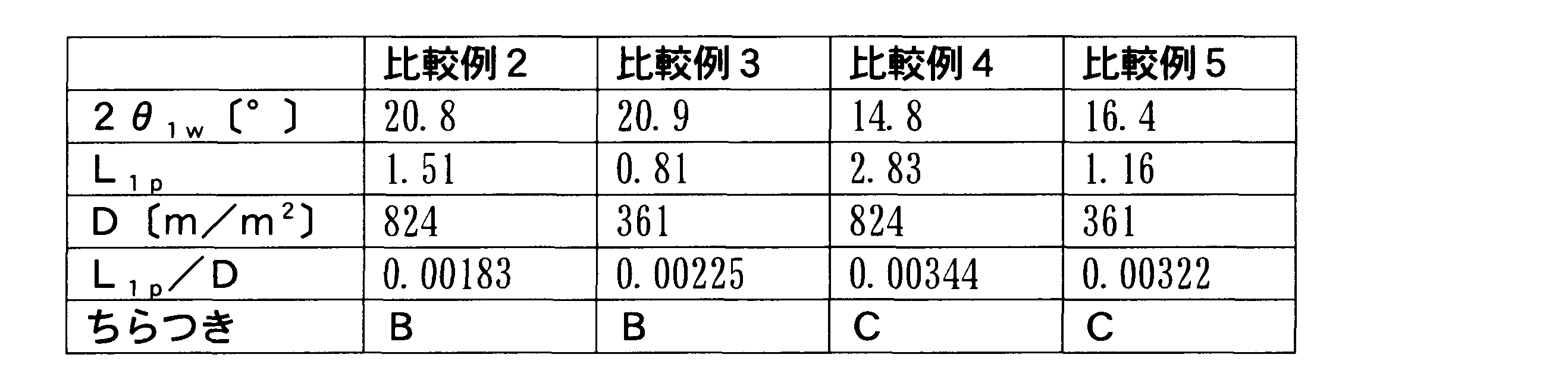
図46及び図47から明らかなように、比較例1~3及び5では、平行光線が合わせ板に対して特定の角度で入射する場合、輝度計52で測定される輝度に幅の広いピークが生じていた。表1及び表2に記載されているように、比較例1~3及び5において、線状導電体での反射光のピークの幅の2θ1wは、16°以上となっている。また、比較例2,4では、平行光線が合わせ板に対して特定の角度で入射する場合、輝度計252で測定される輝度に大きなピークが生じていた。表2に記載されているように、比較例2,4において、線状導電体での反射光のピークでの強さであるパラメータL1pは、1.3以上となっている。さらに、比較例3~5では、パラメータL1pをDで除算した値であって、合わせ板全体での線状導電体での反射光のピークでの強さを示す値であるL1p/Dは、0.002以上となっている。これらは、合わせ板に特定の角度で入射した光の反射光が特定の方向で明るく観察されることを意味する。すなわち、比較例1~5の合わせ板では、ちらつきが発生していると考えられる。実際に比較例1~5の合わせ板では、目視により、ちらつきの発生が確認された。
一方、図46から明らかなように、実施例1~3及び参考例1では、平行光線の合わせ板210への入射角度に対する輝度に幅の広いピークや輝度の大きなピークが生じていなかった。表1に記載されているように、実施例1~3及び参考例1において、線状導電体での反射光のピークの幅の2θ1wは、16°未満となっており、線状導電体での反射光のピークでの強さであるパラメータL1pは、1.3未満となっており、合わせ板全体での線状導電体での反射光のピークでの強さを示すL1p/Dは、0.002未満となっている。これらは、合わせ板に入射した光が特定の方向で明るく観察されることがないことを意味する。すなわち、実施例1~3及び参考例1の合わせ板では、ちらつきの発生は抑制されていると考えられる。実際に実施例1~3及び参考例1の合わせ板では、目視では、ちらつきの発生が確認されなかった。
なお、参考例1の合わせ板では、ちらつきの発生を抑制することはできるが、黒化粗化層の厚さt及び黒化粗化層の線状導電体の幅に対する割合t/Wが50%以上となっている。このため、線状導電体の抵抗が大きくなりすぎて、線状導電体を有するパターン導電体を適切に発熱させることができない。したがって、参考例1の合わせ板は、デフロスタ等の用途で用いることは困難なものとなっている。
上述した発熱板10,110及び合わせ板210は、自動車1,101,201のリアウィンドウ、サイドウィンドウやサンルーフに用いてもよい。また、自動車以外の、鉄道車両、航空機、船舶、宇宙船等の移動体の窓或いは扉の透明部分に用いてもよい。
さらに、発熱板10,110及び合わせ板210は、移動体以外にも、特に室内と室外とを区画する箇所、例えばビルや店舗、住宅の窓或いは扉の透明部分、建物の窓又は扉、冷蔵庫、展示箱、戸棚等の収納乃至保管設備の窓あるいは扉の透明部分等に使用することもできる。
発熱板10,110及び合わせ板210は、デフロスタとして用いられてもよいし、第1基板11及び第2基板12の曇り止めとして用いられてもよい。あるいは、暖房器具(ヒータ)等の他の用途として用いられてもよい。デフロスタ以外の用途についても、発熱板10,110及び合わせ板210は、自動車等の移動体の窓や建物の窓等の透明部分に使用することができる。
なお、当然に、上述した第1の実施の形態乃至第3の実施の形態を適宜に組合せてもよい。例えば、第1の実施の形態及び第2の実施の形態の発熱板10,110における第2暗色層44,144を、第3の実施の形態の合わせ板210における黒化粗化層238としてもよい。この場合、例えば、第1の実施の形態及び第2の実施の形態の発熱板10,110における第1暗色層43,143を、第3の実施の形態の合わせ板210における基材フィルム221に対向する側の面を覆う暗色層としてもよい。あるいは、第1の実施の形態及び第2の実施の形態の発熱板10,110における第1暗色層43,143も、黒化粗化層238としてもよい。
Claims (44)
- 第1方向に離間して配置された第1基板及び第2基板と、
前記第1基板及び前記第2基板の間に配置され、電圧を印加されることで発熱する発熱用導電体と、
前記第1基板と前記第2基板とを接合する接合層と、を備え、
前記発熱用導電体は、前記接合層と隣接し、
前記発熱用導電体は、前記第1基板と接する面を有している、発熱板。 - 第1方向に離間して配置された第1基板及び第2基板と、
前記第1基板及び前記第2基板の間に配置され、電圧を印加されることで発熱する発熱用導電体と、
前記第1基板と前記第2基板とを接合する接合層と、を備え、
前記発熱用導電体は、前記接合層と隣接し、
前記発熱用導電体は、前記第1基板と接し、
前記発熱用導電体の前記第1基板と接する側の表面粗さSzは、3.0μm以下である、発熱板。 - 前記発熱用導電体の前記接合層と隣接する側の面の表面粗さSzは、1.0μmより大きい、請求項1または2に記載の発熱板。
- 第1方向に離間して配置された第1基板及び第2基板と、
前記第1基板及び前記第2基板の間に配置され、電圧を印加されることで発熱する発熱用導電体と、
前記第1基板と前記第2基板とを接合する接合層と、を備え、
前記接合層は、前記発熱用導電体に隣接する第1部分と、前記第1方向において前記第1部分からずれて位置する第2部分と、を含み、
前記第1部分は、前記第2部分と比較して、単位質量あたりの可塑剤の量が少ない、ガラス転移温度が高い、及び、軟化点が高い、のうち少なくともいずれかを満たす、発熱板。 - 前記接合層の前記第1部分は、可塑剤の量が25wt%以下、ガラス転移温度が110℃以上、及び軟化点が60℃以上のうち少なくとも1つを満たす、請求項4に記載の発熱板。
- 前記第1部分の前記第1方向における長さは、前記第2部分の前記第1方向における長さより短い、請求項4または5に記載の発熱板。
- 前記第1部分の前記第1方向における長さは、20μm以上100μm以下である、請求項4乃至6のいずれか一項に記載の発熱板。
- 前記発熱用導電体は、前記第1部分と前記第2部分との間に配置されており、且つ前記第2部分に隣接している、請求項4乃至7のいずれか一項に記載の発熱板。
- 前記発熱用導電体は、前記第1基板と接する、請求項4乃至7のいずれか一項に記載の発熱板。
- 前記発熱用導電体の前記第1基板と接する側の面の表面粗さSzは、3.0μm以下である、請求項9に記載の発熱板。
- 前記発熱用導電体は、複数の線状導電体を含み、
前記線状導電体の長手方向に直交する方向に沿った断面において、前記線状導電体は、前記第1基板と接する面を有している、請求項10に記載の発熱板。 - 前記発熱用導電体の前記接合層と隣接する側の面の表面粗さSzは、1.0μmより大きい、請求項4乃至11のいずれか一項に記載の発熱板。
- 前記発熱用導電体は、複数の線状導電体を含み、
前記接合層は、前記発熱用導電体に隣接する第1部分と、前記第1方向において前記第1部分からずれて位置する第2部分と、を含み、
前記線状導電体の高さに対する前記第1部分の厚さの比は、3以上8以下である、請求項1乃至3または9乃至12のいずれか一項に記載の発熱板。 - 前記線状導電体の高さに対する前記第2部分の厚さの比は、20以上130以下である、請求項13に記載の発熱板。
- 前記発熱用導電体は、複数の線状導電体を含み、
前記線状導電体は、導電層と、前記導電層の表面の少なくとも一部に設けられた暗色層を含む、請求項1乃至14のいずれか一項に記載の発熱板。 - 前記暗色層は、少なくとも前記線状導電体の前記第1基板に対向する側に設けられている、請求項15に記載の発熱板。
- 前記暗色層は、前記導電層の表面のうち、両側面及び前記第2基板に対向する側の面を覆う、請求項15に記載の発熱板。
- 前記発熱用導電体は、複数の線状導電体を含み、
各線状導電体の線幅は、2μm以上20μm以下であり、
各線状導電体の厚さは、1μm以上30μm以下である、請求項1乃至17のいずれか一項に記載の発熱板。 - 前記発熱用導電体は、複数の線状導電体を含み、
前記線状導電体の各位置において、前記線状導電体の線幅に対する高さの比は、0.5以上1.8以下である、請求項1乃至18のいずれか一項に記載の発熱板。 - 前記発熱用導電体は、複数の開口領域を画成するパターンで配置された複数の線状導電体を含み、
前記開口領域の重心間距離の平均は、100μm以上10000μm以下である、請求項1乃至19のいずれか一項に記載の発熱板。 - 前記発熱用導電体は、一方向に延び且つ前記一方向に非平行な方向に隙間を空けて配置される複数の線状導電体を含み、
前記隙間の前記一方向に非平行な方向に沿った長さの平均は、100μm以上12000μm以下である、請求項1乃至19のいずれか一項に記載の発熱板。 - 前記発熱用導電体のシート抵抗は、0.1Ω/□以上1Ω/□以下である、請求項1乃至21のいずれか一項に記載の発熱板。
- 前記発熱用導電体は、複数の線状導電体を含み、
前記線状導電体の断面形状は、台形形状である、請求項1乃至22のいずれか一項に記載の発熱板。 - 前記線状導電体の断面形状は、前記第1基板に接する側が平行な2本の対辺のうちの短くない方の辺となる台形形状である、請求項23に記載の発熱板。
- 前記線状導電体の断面形状は、前記第1基板に接する側が平行な2本の対辺のうちの長くない方の辺となる台形形状である、請求項23に記載の発熱板。
- 前記発熱用導電体は、複数の線状導電体を含み、
前記線状導電体の断面形状は、前記第1基板に対向する側よりも前記第2基板に対向する側おいて幅狭となる、請求項1乃至23のいずれか一項に記載の発熱板。 - 前記発熱用導電体は、複数の線状導電体を含み、
前記線状導電体の断面形状は、前記第1基板に対向する側よりも前記第2基板に対向する側において幅広となる、請求項1乃至23のいずれか一項に記載の発熱板。 - 発熱板に用いられる導電体付きフィルムであって、
電圧を印加されることで発熱する発熱用導電体と、
前記発熱用導電体を支持する基材フィルムと、を備え、
前記基材フィルムは、ヒートシール性を有する、導電体付きフィルム。 - ヒートシール性を有する基材フィルム上に導電膜を設ける工程と、
前記導電膜をパターニングする工程と、
第1基板及び第2基板の間に前記基材フィルムを配置した状態で、前記第1基板及び前記第2基板を互いに向けて加圧・加熱して接合する工程と、を備える、発熱板の製造方法。 - 前記第1基板及び前記第2基板の間にヒートシール性を有する接着フィルムを配置する工程をさらに備え、
前記基材フィルムは、前記接着フィルムと比較して、単位質量あたりの可塑剤の量が少ない、ガラス転移温度が高い、及び、軟化点が高い、のうち少なくともいずれかを満たす、請求項29に記載の発熱板の製造方法。 - 前記第1基板及び前記第2基板の間にヒートシール性を有する接着フィルムを配置する工程をさらに備え、
前記基材フィルムの厚さは、前記接着フィルムの厚さより薄い、請求項29または30に記載の発熱板の製造方法。 - 前記基材フィルムの前記導電膜が設けられた側とは逆側から、可塑剤を添加する工程をさらに備える、請求項29乃至31のいずれか一項に記載の発熱板の製造方法。
- 一対の透明基板と、
前記一対の透明基板の間に配置されたパターン導電体と、を備える合わせ板であって、
前記パターン導電体は、複数の線状導電体を含み、
当該合わせ板に平行光線を照射した状態で、当該合わせ板の前記平行光線を照射される側とは反対側で前記平行光線の照射方向に対して一側へ70°傾斜した方向において測定される輝度であって、前記平行光線の照射方向と前記平行光線の照射方向に対して一側へ70°傾斜した方向との両方に垂直な軸線を中心として当該合わせ板の法線方向を前記平行光線の照射方向に対して前記一側へ角度θ1傾斜させて測定される輝度について、
各傾斜角度θ1で測定された輝度を傾斜角度0°で測定された輝度で除算することで算出される各傾斜角度θ1での規格化輝度を、前記平行光線の照射方向に対する傾斜角度θ1を変数とする次の関数L1n(θ1)に対して、最小二乗法によってフィッティングすることで得られるパラメータL1p、θ1wが、次の関係(i)及び(ii)を満たす、合わせ板。
L1n(θ1)=L1pexp(-2((θ1-θ1p)/θ1w)2)
+cosθ1
2θ1w<16° ・・・(i)
L1p<1.3 ・・・(ii) - 一対の透明基板と、
前記一対の透明基板の間に配置されたパターン導電体と、を備える合わせ板であって、
前記パターン導電体は、複数の線状導電体を含み、
当該合わせ板に平行光線を照射した状態で、当該合わせ板の前記平行光線を照射される側とは反対側で前記平行光線の照射方向に対して一側へ70°傾斜した方向において測定される輝度であって、前記平行光線の照射方向と前記平行光線の照射方向に対して一側へ70°傾斜した方向との両方に垂直な軸線を中心として当該合わせ板の法線方向を前記平行光線の照射方向に対して前記一側へ角度θ1傾斜させて測定される輝度について、
各傾斜角度θ1で測定された輝度を傾斜角度0°で測定された輝度で除算することで算出される各傾斜角度θ1での規格化輝度を、前記平行光線の照射方向に対する傾斜角度θ1を変数とする次の関数L1n(θ1)に対して、最小二乗法によってフィッティングすることで得られるパラメータL1p、θ1wと、前記線状導電体の配置密度D〔m/m2〕とが、次の関係(i)及び(iii)を満たす、合わせ板。
L1n(θ1)=L1pexp(-2((θ1-θ1p)/θ1w)2)
+cosθ1
2θ1w<16° ・・・(i)
L1p/D<0.002 ・・・(iii) - 一対の透明基板と、
前記一対の透明基板の間に配置されたパターン導電体と、を備える合わせ板であって、
前記パターン導電体は、複数の線状導電体を含み、
当該合わせ板の法線方向から他側へ45°傾斜した方向から当該合わせ板に平行光線を照射した状態で、当該合わせ板の前記平行光線を照射される側とは反対側で測定される輝度であって、前記平行光線の照射方向と当該合わせ板の法線方向との両方に垂直な軸線を中心として当該合わせ板の法線方向に対して一側へ角度θ2傾斜した方向で測定される輝度について、
各傾斜角度θ2で測定された輝度を傾斜角度0°で測定された輝度で除算することで算出される各傾斜角度θ2での規格化輝度を、当該合わせ板の法線方向に対する輝度が測定される方向の傾斜角度θ2を変数とする次の関数L2n(θ2)に対して、最小二乗法によってフィッティングすることで得られるパラメータL2p、θ2wが、次の関係(iv)及び(v)を満たす、合わせ板。
L2n(θ2)=L2pexp(-2((θ2-θ2p)/θ2w)2)+1
2θ2w<16° ・・・(iv)
L2p<1.85 ・・・(v) - 前記線状導電体は、その表面に黒化粗化層を有する、請求項33乃至35のいずれか一項に記載の合わせ板。
- 前記黒化粗化層の厚さは、0.7μm以上であり且つ前記線状導電体の幅の50%未満である、請求項36に記載の合わせ板。
- 一対の透明基板と、
前記一対の透明基板の間に配置されたパターン導電体と、を備える合わせ板であって、
前記パターン導電体は、複数の線状導電体を含み、
前記線状導電体は、その表面に黒化粗化層を有し、
前記黒化粗化層の厚さは、0.7μm以上であり且つ前記線状導電体の幅の50%未満である、合わせ板。 - 前記黒化粗化層は、ポーラス状である、請求項36乃至38のいずれか一項に記載の合わせ板。
- 前記黒化粗化層は、前記線状導電体の表面のうち、両側面及び前記一対の透明基板のうちの一方に対向する側の面を覆う、請求項36乃至39のいずれか一項に記載の合わせ板。
- 前記線状導電体の各位置において、前記線状導電体の線幅に対する高さの比は、0.5以上1.8以下である、請求項33乃至40のいずれか一項に記載の合わせ板。
- 前記線状導電体は、当該合わせ板の板面に沿った方向及び当該合わせ板の板面への法線方向に対して傾斜した面を含んでいる、請求項33乃至41のいずれか一項に記載の合わせ板。
- 請求項33乃至42のいずれか一項に記載の合わせ板を備える、デフロスタ。
- 請求項33乃至42のいずれか一項に記載の合わせ板、または請求項43に記載のデフロスタを備える、移動体。
Applications Claiming Priority (4)
| Application Number | Priority Date | Filing Date | Title |
|---|---|---|---|
| JP2018-129477 | 2018-07-06 | ||
| JP2018129477 | 2018-07-06 | ||
| JP2018-146171 | 2018-08-02 | ||
| JP2018146171 | 2018-08-02 |
Publications (1)
| Publication Number | Publication Date |
|---|---|
| WO2020009247A1 true WO2020009247A1 (ja) | 2020-01-09 |
Family
ID=69059201
Family Applications (1)
| Application Number | Title | Priority Date | Filing Date |
|---|---|---|---|
| PCT/JP2019/027058 WO2020009247A1 (ja) | 2018-07-06 | 2019-07-08 | 発熱板、導電体付きフィルム、合わせ板、デフロスタ、移動体及び発熱板の製造方法 |
Country Status (1)
| Country | Link |
|---|---|
| WO (1) | WO2020009247A1 (ja) |
Citations (7)
| Publication number | Priority date | Publication date | Assignee | Title |
|---|---|---|---|---|
| JPH0575147A (ja) * | 1991-09-11 | 1993-03-26 | Nec Corp | 赤外線検出素子 |
| JP2003100422A (ja) * | 2001-09-25 | 2003-04-04 | Toshiba Ceramics Co Ltd | 箔状の抵抗発熱素子及び面状セラミックスヒーター |
| JP2005123132A (ja) * | 2003-10-20 | 2005-05-12 | Kyocera Corp | セラミックスヒータ |
| WO2016080406A1 (ja) * | 2014-11-17 | 2016-05-26 | 大日本印刷株式会社 | 発熱板、導電性パターンシート、乗り物、及び、発熱板の製造方法 |
| WO2017217627A1 (ko) * | 2016-06-16 | 2017-12-21 | 주식회사 엘지화학 | 발열체 및 이의 제조방법 |
| WO2018012553A1 (ja) * | 2016-07-12 | 2018-01-18 | 大日本印刷株式会社 | パターン導電体、導電体付きシート、発熱板、乗り物及びパターン導電体の製造方法 |
| JP2018037263A (ja) * | 2016-08-31 | 2018-03-08 | 大日本印刷株式会社 | 乗り物用ガラス装置、及び該装置に用いられる加熱電極シートの製造方法 |
-
2019
- 2019-07-08 WO PCT/JP2019/027058 patent/WO2020009247A1/ja active Application Filing
Patent Citations (7)
| Publication number | Priority date | Publication date | Assignee | Title |
|---|---|---|---|---|
| JPH0575147A (ja) * | 1991-09-11 | 1993-03-26 | Nec Corp | 赤外線検出素子 |
| JP2003100422A (ja) * | 2001-09-25 | 2003-04-04 | Toshiba Ceramics Co Ltd | 箔状の抵抗発熱素子及び面状セラミックスヒーター |
| JP2005123132A (ja) * | 2003-10-20 | 2005-05-12 | Kyocera Corp | セラミックスヒータ |
| WO2016080406A1 (ja) * | 2014-11-17 | 2016-05-26 | 大日本印刷株式会社 | 発熱板、導電性パターンシート、乗り物、及び、発熱板の製造方法 |
| WO2017217627A1 (ko) * | 2016-06-16 | 2017-12-21 | 주식회사 엘지화학 | 발열체 및 이의 제조방법 |
| WO2018012553A1 (ja) * | 2016-07-12 | 2018-01-18 | 大日本印刷株式会社 | パターン導電体、導電体付きシート、発熱板、乗り物及びパターン導電体の製造方法 |
| JP2018037263A (ja) * | 2016-08-31 | 2018-03-08 | 大日本印刷株式会社 | 乗り物用ガラス装置、及び該装置に用いられる加熱電極シートの製造方法 |
Similar Documents
| Publication | Publication Date | Title |
|---|---|---|
| US20210307120A1 (en) | Heating electrode device, electrical heating glass, heat-generating plate, vehicle, window for building, sheet with conductor, conductive pattern sheet, conductive heat-generating body, laminated glass, and manufacturing method for conductive heat-generating body | |
| WO2016080406A1 (ja) | 発熱板、導電性パターンシート、乗り物、及び、発熱板の製造方法 | |
| JP7220994B2 (ja) | パターン導電体、導電体付きシート、発熱板、乗り物及びパターン導電体の製造方法 | |
| JP6295885B2 (ja) | 合わせガラス、乗り物および窓 | |
| JP6913294B2 (ja) | 発熱板、導電体付きシート、乗り物及び建築物用窓 | |
| JP2016141210A (ja) | 発熱板、導電性パターンシートおよび発熱板を備えた乗り物 | |
| JP7310366B2 (ja) | 合わせ板、デフロスタ、移動体 | |
| WO2020009247A1 (ja) | 発熱板、導電体付きフィルム、合わせ板、デフロスタ、移動体及び発熱板の製造方法 | |
| JP6951674B2 (ja) | 発熱用導電体、導電体付きシート、発熱板および乗り物 | |
| JP2017212047A (ja) | 導電性発熱体、合わせガラスおよび乗物 | |
| JP2019197727A (ja) | 発熱板、導電体付きフィルム及び発熱板の製造方法 | |
| JP7385833B2 (ja) | パターン導電体、発熱板及び移動体 | |
| JP7033264B2 (ja) | 導電体付きシート、発熱板および乗り物 | |
| JP7310370B2 (ja) | 発熱板、導電体付きフィルム及び発熱板の製造方法 | |
| JP6828239B2 (ja) | 発熱板、導電性パターンシートおよび発熱板を備えた乗り物 | |
| JP2019117804A (ja) | 発熱板及び乗り物 | |
| JP7356640B2 (ja) | 発熱用導電体、発熱板、移動体 | |
| JP6757515B2 (ja) | 合わせガラス及び乗り物 | |
| JP6478150B2 (ja) | 発熱板、発熱板を備えた乗り物、及び、発熱板の製造方法 | |
| JP6540037B2 (ja) | 発熱板及び乗り物 | |
| JP2018092881A (ja) | 発熱用導電体、発熱板および乗り物 | |
| JP6670466B2 (ja) | 発熱板、乗り物及び建築物用窓 | |
| JP7405096B2 (ja) | パターン導電体、バスバー付きパターン導電体、合わせ板、仕切部材及び移動体 | |
| JP2018055942A (ja) | 発熱用導電体、導電体付きシート、発熱板、乗り物および建築物 | |
| JP6770703B2 (ja) | パターン導電体、発熱用導電体、導電体付きシート、発熱板、乗り物および建築物 |
Legal Events
| Date | Code | Title | Description |
|---|---|---|---|
| 121 | Ep: the epo has been informed by wipo that ep was designated in this application |
Ref document number: 19830432 Country of ref document: EP Kind code of ref document: A1 |
|
| NENP | Non-entry into the national phase |
Ref country code: DE |
|
| 122 | Ep: pct application non-entry in european phase |
Ref document number: 19830432 Country of ref document: EP Kind code of ref document: A1 |