WO2020004289A1 - 透明導電フィルム積層体の製造方法 - Google Patents
透明導電フィルム積層体の製造方法 Download PDFInfo
- Publication number
- WO2020004289A1 WO2020004289A1 PCT/JP2019/024849 JP2019024849W WO2020004289A1 WO 2020004289 A1 WO2020004289 A1 WO 2020004289A1 JP 2019024849 W JP2019024849 W JP 2019024849W WO 2020004289 A1 WO2020004289 A1 WO 2020004289A1
- Authority
- WO
- WIPO (PCT)
- Prior art keywords
- transparent conductive
- film
- conductive film
- protective film
- transparent
- Prior art date
- Legal status (The legal status is an assumption and is not a legal conclusion. Google has not performed a legal analysis and makes no representation as to the accuracy of the status listed.)
- Ceased
Links
Images



Classifications
-
- B—PERFORMING OPERATIONS; TRANSPORTING
- B32—LAYERED PRODUCTS
- B32B—LAYERED PRODUCTS, i.e. PRODUCTS BUILT-UP OF STRATA OF FLAT OR NON-FLAT, e.g. CELLULAR OR HONEYCOMB, FORM
- B32B7/00—Layered products characterised by the relation between layers; Layered products characterised by the relative orientation of features between layers, or by the relative values of a measurable parameter between layers, i.e. products comprising layers having different physical, chemical or physicochemical properties; Layered products characterised by the interconnection of layers
- B32B7/04—Interconnection of layers
- B32B7/06—Interconnection of layers permitting easy separation
-
- C—CHEMISTRY; METALLURGY
- C23—COATING METALLIC MATERIAL; COATING MATERIAL WITH METALLIC MATERIAL; CHEMICAL SURFACE TREATMENT; DIFFUSION TREATMENT OF METALLIC MATERIAL; COATING BY VACUUM EVAPORATION, BY SPUTTERING, BY ION IMPLANTATION OR BY CHEMICAL VAPOUR DEPOSITION, IN GENERAL; INHIBITING CORROSION OF METALLIC MATERIAL OR INCRUSTATION IN GENERAL
- C23C—COATING METALLIC MATERIAL; COATING MATERIAL WITH METALLIC MATERIAL; SURFACE TREATMENT OF METALLIC MATERIAL BY DIFFUSION INTO THE SURFACE, BY CHEMICAL CONVERSION OR SUBSTITUTION; COATING BY VACUUM EVAPORATION, BY SPUTTERING, BY ION IMPLANTATION OR BY CHEMICAL VAPOUR DEPOSITION, IN GENERAL
- C23C14/00—Coating by vacuum evaporation, by sputtering or by ion implantation of the coating forming material
- C23C14/22—Coating by vacuum evaporation, by sputtering or by ion implantation of the coating forming material characterised by the process of coating
- C23C14/34—Sputtering
-
- C—CHEMISTRY; METALLURGY
- C23—COATING METALLIC MATERIAL; COATING MATERIAL WITH METALLIC MATERIAL; CHEMICAL SURFACE TREATMENT; DIFFUSION TREATMENT OF METALLIC MATERIAL; COATING BY VACUUM EVAPORATION, BY SPUTTERING, BY ION IMPLANTATION OR BY CHEMICAL VAPOUR DEPOSITION, IN GENERAL; INHIBITING CORROSION OF METALLIC MATERIAL OR INCRUSTATION IN GENERAL
- C23C—COATING METALLIC MATERIAL; COATING MATERIAL WITH METALLIC MATERIAL; SURFACE TREATMENT OF METALLIC MATERIAL BY DIFFUSION INTO THE SURFACE, BY CHEMICAL CONVERSION OR SUBSTITUTION; COATING BY VACUUM EVAPORATION, BY SPUTTERING, BY ION IMPLANTATION OR BY CHEMICAL VAPOUR DEPOSITION, IN GENERAL
- C23C14/00—Coating by vacuum evaporation, by sputtering or by ion implantation of the coating forming material
- C23C14/58—After-treatment
-
- H—ELECTRICITY
- H01—ELECTRIC ELEMENTS
- H01B—CABLES; CONDUCTORS; INSULATORS; SELECTION OF MATERIALS FOR THEIR CONDUCTIVE, INSULATING OR DIELECTRIC PROPERTIES
- H01B13/00—Apparatus or processes specially adapted for manufacturing conductors or cables
Definitions
- the present invention relates to a method for producing a transparent conductive film laminate.
- a touch panel for detecting an input position using a transparent conductive film has been known.
- Various configurations of the touch panel have been studied in the past, but a capacitive touch panel is known as an example.
- the touch panel disclosed in Patent Literature 1 is configured such that a dielectric layer is interposed between a pair of transparent conductive films each having a transparent conductive layer having a predetermined pattern shape, and a finger or the like is operated on an operation surface.
- the touch position can be detected by utilizing the change in capacitance caused by being grounded via the human body.
- the above-mentioned touch panel is used by mounting it on the surface of a liquid crystal display or a CRT.
- the transparent conductive film that constitutes the touch panel is vulnerable to mechanical rubbing and hitting, so it must be handled with care during the manufacturing process. Attention is necessary.
- the appearance is important, so that the surface must be protected from damage. By bonding, the transparent conductive film is prevented from being damaged.
- a transparent conductive film provided with such a protective film is obtained by bonding a protective film to a transparent film via an adhesive layer, and then opposing the surface on which the protective film is bonded.
- a transparent conductive layer (ITO) is formed on the surface of the transparent film on the side, and a heat treatment for crystallizing the transparent conductive layer (ITO) is performed, or a transparent conductive layer (ITO) is formed on one surface of the transparent film. ),
- a protective film is adhered via an adhesive layer to the surface of the transparent film opposite to the surface on which the transparent conductive layer (ITO) is formed, and then the transparent conductive layer (ITO) is crystallized. It is manufactured by performing a heat treatment for conversion.
- wiring for signal detection is formed on the transparent conductive film.
- this wiring is formed by, for example, applying a silver paste in a predetermined form on a transparent conductive film and then performing a heat treatment for firing.
- a transparent conductive film with a protective film transparent conductive film laminate
- a transparent conductive layer transparent conductive layer
- the protective film a film that is hard to generate a precipitate (oligomer) even when a heat treatment for crystallizing the transparent conductive layer (ITO) and a heat treatment for forming the wiring is performed is specially selected. It has to be used, and there is a problem that the selection range of the protective film is narrow.
- an object of the present invention is to provide a method for manufacturing a transparent conductive film laminate that can increase the selection range of a protective film.
- the object of the present invention is to form a transparent conductive film on one side of a transparent film by forming a transparent conductive layer, and forming the transparent conductive film on the transparent conductive film at a temperature of at least 135 ° C. for at least 0.2 hours.
- a heat treatment step of performing a heat treatment comprising a protection film lamination step of protecting the other surface of the transparent film and bonding a peelable protection film, the protection film lamination step is performed after the heat treatment step
- This is achieved by a method for producing a transparent conductive film laminate, which is characterized in that:
- the transparent conductive film forming step preferably includes a step of forming the transparent conductive layer on one surface of the transparent film by a sputtering method at least at 180 ° C. or less.
- the heat treatment step is a step of crystallizing the transparent conductive layer.
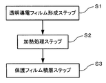
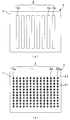
- FIG. 1 It is a block diagram for explaining the manufacturing method of the transparent conductive film layered product concerning the present invention. It is a schematic cross section explanatory view for explaining the process in the transparent conductive film forming step. (A) and (b) are schematic plan views for explaining a pattern form of a transparent conductive layer to be formed. It is a schematic cross section explanatory view for explaining the process in the protective film laminating step. It is a graph which shows the relationship between the thickness (micrometer) of a protective film main body, and a heat shrinkage rate (%).
- the manufacturing method of the present invention includes a transparent conductive film 3 forming step S1, a heat treatment step S2, and a protective film 4 laminating step S3.
- a numerical value connected by “to” means a numerical range including the numerical value before and after “to” as a lower limit and an upper limit.
- Transparent conductive film 3 forming step S1 is a step of forming transparent conductive layer 2 on one surface of transparent film 1 to form transparent conductive film 3, as shown in the schematic cross-sectional explanatory view of FIG.
- the transparent film 1 examples include polyethylene terephthalate (PET), polyimide (PI), polyethylene naphthalate (PEN), polyether sulfone (PES), polyether ether ketone (PEEK), polycarbonate (PC), and polypropylene (PP). ), Polyamide (PA), polyacrylic (PAC), acrylic, amorphous polyolefin resin, cyclic polyolefin resin, aliphatic cyclic polyolefin, norbornene-based thermoplastic transparent resin, etc., and two or more of these flexible films. Are formed.
- the lower limit of the thickness of the transparent film 1 is preferably 10 ⁇ m or more, more preferably 20 ⁇ m or more, further preferably 50 ⁇ m or more, and the upper limit is preferably 300 ⁇ m or less, more preferably 200 ⁇ m or less, and still more preferably 125 ⁇ m or less. Is mentioned.
- an easy-adhesion layer may be formed on the surface of the transparent film 1 and a surface treatment such as a corona treatment may be performed in advance to improve adhesion.
- a hard coat layer (not shown) may be provided on one side or both sides of the transparent film 1.
- the hard coat layer is a layer for securing the surface strength of the transparent film 1, and is formed by applying and drying the above-mentioned material on the surface of the transparent film 1 by using a known printing method, coating method, or the like. Can be.
- the thickness of the hard coat layer after drying is preferably set, for example, in the range of 1 ⁇ m to 5 ⁇ m.
- an ionizing radiation curable material or a thermosetting material can be used.
- the ionizing radiation-curable material for example, an acrylic material can be used.
- acrylic material examples include monofunctional, difunctional or trifunctional (meth) acrylate compounds such as acrylic acid or methacrylic acid ester of polyhydric alcohol, diisocyanate and polyhydric alcohol, and hydroxyester of acrylic acid or methacrylic acid.
- Polyfunctional urethane (meth) acrylate compounds such as those synthesized from As the thermosetting material, for example, organopolysiloxane can be used.
- the layer made of organopolysiloxane is a layer obtained by hydrolysis and dehydration polycondensation according to a wet method using organosiloxane as a starting material, and forms a three-dimensional network polymer network based on a siloxane (Si—O) skeleton. Is configured.
- indium tin oxide As the material of the transparent conductive layer 2, indium tin oxide (ITO) can be preferably used.
- ITO indium tin oxide
- indium oxide, antimony-added tin oxide, fluorine-added tin oxide, aluminum Transparent conductive materials such as added zinc oxide, gallium added zinc oxide, silicon added zinc oxide, zinc oxide-tin oxide, indium oxide-tin oxide, zinc oxide-indium oxide-magnesium oxide, zinc oxide, and tin oxide film
- a metal material such as tin, copper, aluminum, nickel, and chromium, a metal oxide material, and the like, or a material obtained by combining two or more of these materials can also be used.
- Examples of the method for forming the transparent conductive layer 2 include a PVD method such as a sputtering method, a vacuum evaporation method, and an ion plating method, a CVD method, a coating method, and a printing method.
- a PVD method such as a sputtering method, a vacuum evaporation method, and an ion plating method
- CVD method a coating method
- a printing method a printing method.
- the transparent conductive layer 2 is formed by a sputtering method, it is preferable to form the film under a temperature condition of at least 180 ° C. or less. More preferably, the temperature condition is 170 ° C. or lower, further preferably, 160 ° C. or lower.
- the thickness of the transparent conductive layer 2 to be formed for example, the lower limit is preferably 10 nm or more, more preferably 15 nm or more, and still more preferably 20 nm or more, and the upper limit is preferably 100 nm or less. More preferably, the thickness is 90 nm or less, and further preferably, 80 nm or less.
- the transparent conductive layer 2 to be formed may be formed by being patterned into a predetermined shape.
- the transparent conductive layer 2 can be formed as an aggregate of a plurality of strip-shaped conductive portions 2a extending in parallel.
- the pattern shape of the transparent conductive layer 2 is not limited to the form shown in FIG. 3A, and may be any shape as long as a contact point such as a finger can be detected.
- the band-shaped conductive portion 2a in the transparent conductive layer 2 may have a configuration in which a plurality of rhombus-shaped electrode portions 21 are linearly connected.
- the transparent conductive layer 2 having a predetermined pattern shape is obtained by forming a transparent conductive film with a predetermined thickness on the transparent film 1 and then forming a mask portion having a desired pattern shape on the surface of the transparent conductive film. After the exposed portion is etched away with an acid solution or the like, the mask portion can be formed by dissolving or peeling the mask portion with an alkali solution or the like.
- the heat treatment step S2 is a step of heating the transparent conductive layer 2 formed on one surface of the transparent film 1, and a step of heating the transparent conductive film 3 at a temperature of at least 135 ° C. for at least 0.2 hours. It is.
- the transparent conductive layer 2 is formed of indium tin oxide (ITO)
- a step of crystallizing the indium tin oxide (ITO) to reduce the resistance is performed.
- the heating temperature in the heat treatment step S2 can be appropriately selected from a range of 135 ° C. or more and 150 ° C. or less, for example, 135 ° C., 140 ° C., and 150 ° C.
- the heating time can be appropriately selected from the range of 0.2 hours to 1 hour, such as 0.2 hours, 0.5 hours, and 1 hour. Note that the heat treatment step is preferably performed at a high temperature in terms of productivity.
- the heat treatment apparatus provided in the heat treatment step S2 is not particularly limited.
- an RTA (Rapid Thermal) equipment such as an electric furnace, a GRTA (Gas Rapid Thermal Anneal) apparatus, or an LRTA (Lamp Rapid Thermal Anneal) apparatus is used.
- the GRTA apparatus is an apparatus that performs a heat treatment using a high-temperature gas.
- the LRTA apparatus is an apparatus that heats an object to be processed by radiation of light (electromagnetic wave) emitted from a lamp such as a halogen lamp, a metal halide lamp, a xenon arc lamp, a carbon arc lamp, a high-pressure sodium lamp, and a high-pressure mercury lamp.
- the protective film 4 laminating step S3 is a step performed after the above-described heat treatment step S2, and as shown in the schematic cross-sectional explanatory view of FIG. 4 is a step of bonding.
- the protective film 4 protects the surface of the transparent film 1 opposite to the surface on which the transparent conductive layer 2 is formed, and includes a protective film main body 41 and an adhesive layer provided on one side of the protective film main body 41. 42. This protective film 4 is laminated on the transparent film 1 so as to be peelable.
- the material forming the protective film main body 41 is not particularly limited, and for example, polyester such as polyethylene terephthalate (PET) and polyethylene naphthalate (PEN), polyphenylene sulfide (PPS), polycarbonate, polymethyl methacrylate, polystyrene, and polychlorinated chloride Vinyl, polyethylene, polypropylene, polyethylene / polypropylene blend, polyamide, polyimide, cellulose acetate, polysulfone, polyethersulfone, polyethersulfone (PES), polyetheretherketone (PEEK), polycarbonate (PC), polyacryl ( PAC), acrylic, amorphous polyolefin resin, cyclic polyolefin resin, aliphatic cyclic polyolefin, norbornene thermoplastic Such flexible film, such as a bright resins.
- polyester such as polyethylene terephthalate (PET) and polyethylene naphthalate (PEN), polyphenylene sulfide (PPS
- PET when transparency and heat resistance are required, PET, PEN, PPS, amorphous polyolefin resin, cyclic polyolefin resin, and aliphatic cyclic polyolefin are preferable. Since the material constituting 41 preferably has a heat shrinkage equivalent to that of the transparent film 1, it is preferable that the material is the same.
- the thickness of the protective film body 41 is not particularly limited, but the lower limit is preferably 10 ⁇ m or more, more preferably 20 ⁇ m or more, further preferably 50 ⁇ m or more, and the upper limit is preferably 300 ⁇ m or less, more preferably 200 ⁇ m, more preferably 125 ⁇ m. If the thickness is too small, the strength at the time of peeling the surface protection film 41 and the surface protection function tend to be insufficient. On the other hand, if the thickness is too large, it tends to be disadvantageous in terms of handleability and cost.
- a removable pressure-sensitive adhesive (acrylic, rubber, synthetic rubber, etc.) can be used without any particular limitation. Among them, an acrylic pressure-sensitive adhesive whose adhesive strength is easily controlled by the composition is preferable.
- the method of bonding the protective film 4 having the above-described configuration to the other surface of the transparent film 1 is not particularly limited, but a preferable bonding method is a so-called roll-to-roll method.
- the protective film 4 is attached to the other surface side of the transparent film 1.
- the heat load applied to the manufactured transparent conductive film laminate is caused when the wiring is formed. This is only a heat treatment or a post-etching drying step when processing the transparent conductive layer into a desired pattern, and the heat load when heating and firing the transparent conductive layer 2 is not applied. The heat load can be reduced, and the generation of precipitates (oligomers) can be effectively suppressed.
- the transparent conductive film 3 does not become cloudy, and the appearance is performed in the manufacturing process of the transparent conductive film 3 and the manufacturing process of the touch panel using the transparent conductive film 3.
- damage such as a scratch on the transparent conductive film 3 can be found earlier and more reliably, and a high-precision appearance inspection can be performed.
- a transparent conductive film laminate (the transparent conductive film 3 with the protective film 4) is continuously produced while being wound up in a roll shape by a so-called roll-to-roll method.
- the transparent conductive layer 2 (ITO film) and the surface of the protective film 4 it is possible to effectively prevent the precipitate (oligomer) from contaminating the surface of the transparent conductive layer 2 (ITO film). Become.
- the precipitate (oligomer) is used as the protective film 4 as in the related art.
- the need to specially select and use those which are unlikely to cause) is reduced, and a transparent conductive film laminate (transparent conductive film 3 with protective film 4) is manufactured using a wide variety of protective films 4. Becomes possible.
- the lower limit of the thickness of the transparent conductive film laminate is preferably 100 ⁇ m, more preferably 125 ⁇ m or more, and the upper limit.
- the thickness is preferably 250 ⁇ m, more preferably 200 ⁇ m or less.
- Samples A to H were prepared as transparent conductive film laminates to be subjected to the test.
- Samples A to D are manufactured by the manufacturing method according to the present invention, and samples E to H are manufactured by the conventional manufacturing method. More specifically, in Samples A to D, an ITO film (transparent conductive layer 2) is formed on one surface of the transparent film 1 by a sputtering method to form a transparent conductive film 3, and then the crystal of the ITO film is formed.
- the transparent film 1 is manufactured by performing a heat treatment for a chemical conversion treatment, and then bonding a peelable protective film 4 on the other surface of the transparent film 1. In the heat treatment, heating is performed at a temperature of 150 ° C. for one hour.
- an ITO film (transparent conductive layer 2) is formed on one surface of the transparent film 1 by a sputtering method to form a transparent conductive film 3, and then peeled off on the other surface of the transparent film 1. It is manufactured by performing a heat treatment for crystallizing the transparent conductive layer (ITO) after bonding the possible protective film 4. In the heat treatment, heating is performed at a temperature of 150 ° C. for one hour.
- a hard coat formed by applying and drying an acrylic ionizing radiation-curable hard coat layer on both surfaces of a polyethylene terephthalate film having a thickness of 100 ⁇ m by a roll-to-roll coating method A coated film is adopted as the transparent film 1, and an SiO 2 layer is formed on the transparent film 1 by a roll-to-roll magnetron sputtering method, and then an ITO layer (transparent conductive layer 2) having a thickness of 40 nm is formed. ) Is formed.
- the obtained roll-shaped transparent conductive film was cut into a rectangular shape of A4 size to obtain a material for forming a protective film laminate.
- a polyethylene terephthalate film was used as the protective film main body 41 in each of the samples A to I, and an adhesive layer formed of an acrylic adhesive was formed on one surface of the protective film main body 41.
- the roll-shaped protective film provided with 42 was cut out into an A4 size rectangular shape, and used as a material for forming a protective film laminate.
- the thickness of the protective film 4 was the same as that of Sample A and Sample E of 60 ⁇ m (thickness of the protective film body 41). (38 ⁇ m); the thickness of the pressure-sensitive adhesive layer 42 (22 ⁇ m)) and the sample B and the sample F having the same thickness of 50 ⁇ m (thickness of the protective film main body 41 (38 ⁇ m); thickness of the pressure-sensitive adhesive layer 42 ( 12 ⁇ m)).
- sample C and the sample G are configured to have the same thickness of 110 ⁇ m (the thickness of the protective film main body 41 (100 ⁇ m); the thickness of the pressure-sensitive adhesive layer 42 (10 ⁇ m)), and the sample D and the sample H are configured to have the same thickness of 150 ⁇ m.
- the thickness of the protective film main body 41 125 ⁇ m; the thickness of the pressure-sensitive adhesive layer 42 (25 ⁇ m)).
- Table 1 the values of the heat shrinkage (%) of each protective film main body 41 in Samples A to H when subjected to a heat treatment at 150 ° C. ⁇ 1 hour are also described. .
- the MD direction means a resin flowing direction when the protective film main body is formed
- the TD direction means a direction perpendicular to the MD direction.
- the thermal shrinkage (%) of the protective film main body tends to decrease as the thickness of the protective film main body 41 increases.
- Treatment and "assuming the case where the wiring is baked on the surface", a heat treatment is performed at a temperature of 120 ° C. for 30 minutes, and it is determined whether or not the heat treatment causes haze on the surface.
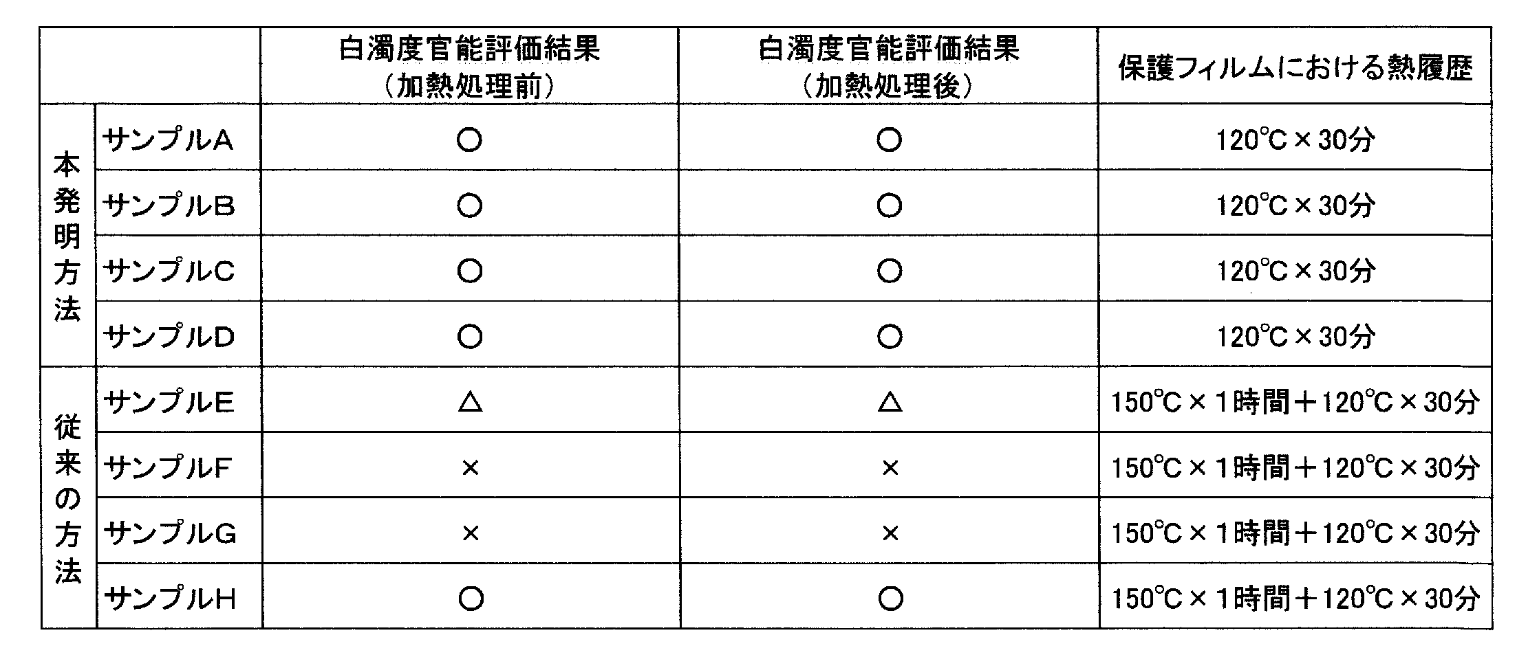
- a sensory test was performed. Table 2 shows the results of the sensory test (sensory evaluation of cloudiness). For reference, the results of the sensory evaluation of the white turbidity of Samples A to H and the heat history applied to the protective film 4 before the heat treatment at a temperature of 120 ° C. for 30 minutes are also shown.
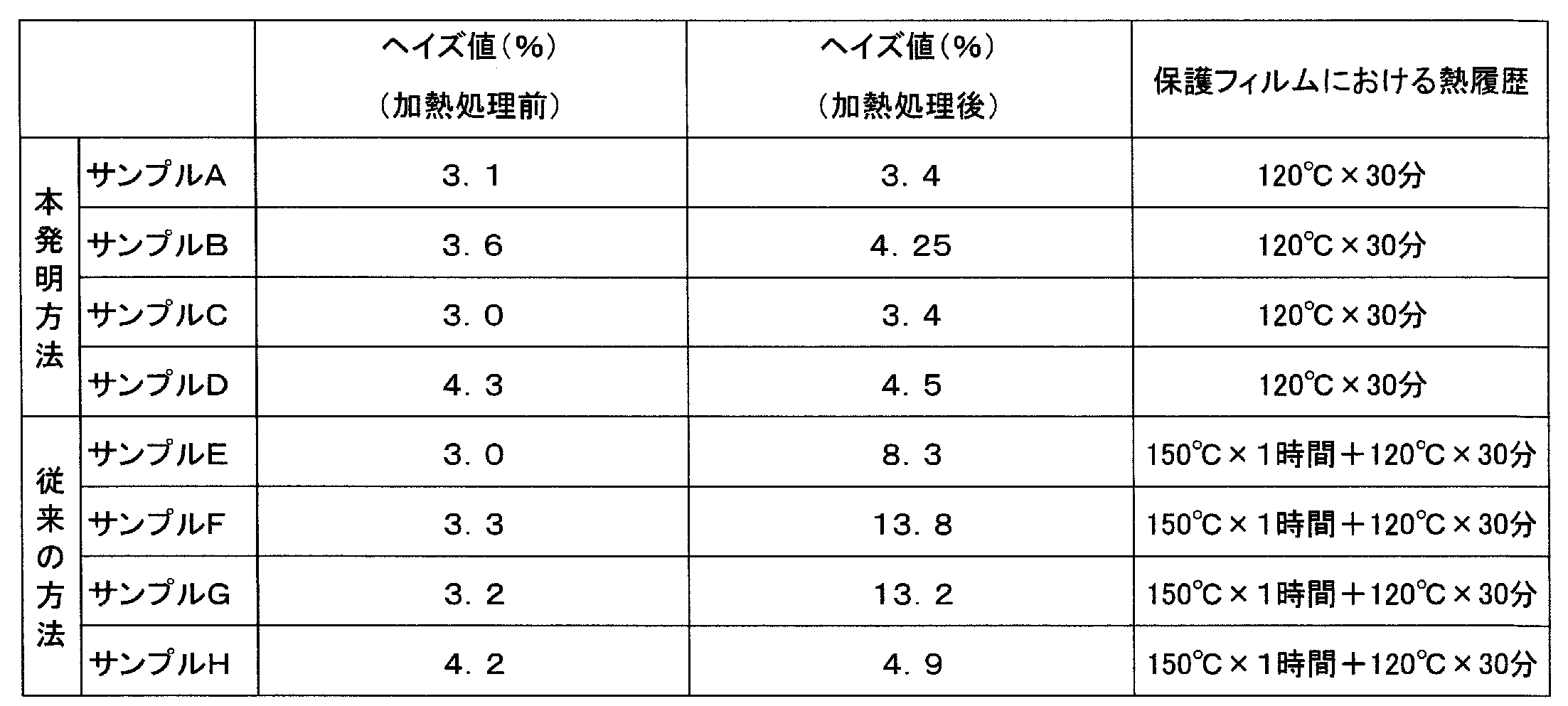
- the haze values of the samples A to H before and after the heat treatment after bonding the protective film 4 to the transparent conductive film 3 were also measured, and the measurement results are also shown in Table 3.
- the haze values of Samples A to H and the heat history applied to the protective film 4 before the heat treatment at a temperature of 120 ° C. for 30 minutes are also shown.
- the haze value was measured by "NDH-5000" manufactured by Nippon Denshoku Industries Co., Ltd. based on JIS K7136.
- calibration was performed using a black iron plate having a hole of ⁇ 7 mm, and a sample was placed in the hole of the black iron plate at the time of measurement to measure.
- the samples B and C manufactured by the manufacturing method according to the present invention are compared with the samples F and G manufactured by the conventional manufacturing method.
- the thickness of the pressure-sensitive adhesive layer of the protective film in each of Samples B and C (Samples F and G) is about 10 ⁇ m, and that of other Samples A and D (Samples G and H). It is presumed that the thickness is smaller than that of).
- the preferable range of the pressure-sensitive adhesive layer of the protective film is 17 ⁇ m or less, more preferably 15 ⁇ m or less, and further preferably 12 ⁇ m or less.
- the numerical value of 17 ⁇ m which is the upper limit of the numerical range of the pressure-sensitive adhesive layer, is calculated as an arithmetic average of the pressure-sensitive adhesive layer thickness of Sample A: 22 ⁇ m and the pressure-sensitive adhesive layer thickness of Sample B: 12 ⁇ m.
- the haze value after the heat treatment is as small as 7% or less for the transparent conductive film laminates of Samples A to D manufactured by the manufacturing method of the present invention. Further, it can be seen that the change in the haze value before and after the heat treatment at a temperature of 120 ° C. for 30 minutes is small, and the rise value of the haze value falls within 1.0 point or less in each case. Specifically, for sample A, the haze value before the heat treatment was 3.1%, while the haze value after the heat treatment was 3.4%, and the increase was 0.3 points. For sample B, the haze value before the heat treatment was 3.6%, while the haze value after the heat treatment was 4.2%, and the increase was 0.6 points.
- the samples E, F, and G other than the sample H have a haze value of more than 7%. I understand that there is.
- the usable protective film 4 is the protective film 4 according to the sample H, in which the precipitate (oligomer) is unlikely to be generated among the protective films 4 according to the samples E to H.
- the protective film 4 according to all of the samples A to D can be used, and a precipitate (oligomer) hardly occurs.
- the burden of specially selecting the protective film 4 can be reduced, the range of available protective films 4 can be greatly expanded, and the transparent conductive film laminate (the transparent conductive film 3 with the protective film 4) can be efficiently formed. It can be manufactured.
- the protective films 4 according to the samples A to D are the same as the protective films 4 according to the samples E to H, respectively.
- the inventor also conducted a test for measuring the peel strength of the protective film 4 with respect to the transparent conductive film laminates according to Samples A to H. The test contents and results are shown below.
- each of the samples A to H was cut into a strip having a width of 20 mm.
- the peeling strength of a sample cut to a width of 20 mm at 180 ° peeling was measured using a surface property measuring device “HEIDON-14DR” manufactured by Shinto Chemical Co., Ltd. Note that the peeling speed (tensile speed) was 0.2 m / min.
- Table 4 The results of the peel strength test are shown in Table 4 below.
- Table 5 shows the results of the sensory evaluation on the peel strength.
- "the thing which is judged that it is easily peelable and can be used suitably is set to” O "
- "the thing which is judged that it is slightly hard to peel but is usable is " ⁇ ”.
- "x" indicates that it is difficult to peel off and may damage the ITO film or the like and is determined to be unusable.
- Tables 4 and 5 also show the peel strength test results or peel strength sensory evaluation results of Samples A to H before the heat treatment and the heat history applied to the protective film 4. it's shown.
- the peel strength of the protective film 4 after the heat treatment was 6. It is 5 gf / cm or less, which indicates that the film can be easily peeled off.
- the transparent conductive film laminates according to the samples E to H manufactured by the conventional manufacturing method the samples F to H resulted in a low peel strength, but the sample E had the peel strength low.
- the strength is as high as 10.50 gf / cm, and the protective film 4 is hardly peeled off. If the protective film 4 is peeled off, there is a concern that the transparent conductive layer 2 (ITO film) may be damaged. It turns out that it is.
- the upper limit value of the peel strength that does not damage the transparent conductive layer 2 (ITO film) or the like when the protective film 4 is peeled off is as follows. Since it can be estimated that the value is around 9.0 gf / cm, which is a numerical value between 10.50 gf / cm which is the measurement result and 7.25 gf / cm which is the measurement result before the heat treatment of Sample A, It can be said that the peel strength of the protective film 4 included in the transparent conductive film laminate is preferably set to 9.0 gf / cm or less.
- the protective films 4 that can be used are three types of the samples FH among the four types of the protective films 4 according to the samples EH.
- the manufacturing method according to the present invention it is possible to use four types of protective films 4 for all of the samples A to D, and from the viewpoint of the peeling property, the range of options of the usable protective films 4 is increased. It can be seen that the transparent conductive film laminate (the transparent conductive film 3 with the protective film 4) can be efficiently manufactured.
- the manufacturing method according to the present invention is employed, the heat load applied to the protective film 4 can be reduced, thereby suppressing an increase in the peel strength of the pressure-sensitive adhesive layer 42 of the protective film as compared with the conventional manufacturing method. You can see that it is done.
Landscapes
- Chemical & Material Sciences (AREA)
- Engineering & Computer Science (AREA)
- Chemical Kinetics & Catalysis (AREA)
- Materials Engineering (AREA)
- Mechanical Engineering (AREA)
- Metallurgy (AREA)
- Organic Chemistry (AREA)
- Manufacturing & Machinery (AREA)
- Manufacturing Of Electric Cables (AREA)
- Physical Vapour Deposition (AREA)
- Non-Insulated Conductors (AREA)
Abstract
保護フィルムの選択幅を拡げることができる透明導電フィルム積層体の製造方法を提供する。 透明フィルムの一方面に透明導電層を成膜し、透明導電フィルムを形成する透明導電フィルム形成ステップと、前記透明導電フィルムを少なくとも135℃の温度で少なくとも0.2時間加熱処理を行う加熱処理ステップと、前記透明フィルムの他方面を保護し、剥離可能な保護フィルムを貼り合わせる保護フィルム積層ステップとを備え、前記保護フィルム積層ステップは、前記加熱処理ステップ後に実施されることを特徴とする透明導電フィルム積層体の製造方法。
Description
本発明は、透明導電フィルム積層体の製造方法に関する。
従来、透明導電フィルムを用いて入力位置を検出するためのタッチパネルが知られている。このタッチパネルの構成は、従来から種々検討されているが、一例として静電容量式のタッチパネルが知られている。例えば、特許文献1に開示されたタッチパネルは、それぞれ所定のパターン形状を有する透明導電層を備えた一対の透明導電フィルムの間に誘電体層が介在されて構成されており、指などが操作面に触れると、人体を介して接地されることによる静電容量の変化を利用して、タッチ位置を検出することができる。
上述のタッチパネルは、液晶表示装置やCRTなどの表面に装着して使用されるが、タッチパネルを構成する透明導電フィルムは、機械的なこすれや打撃に弱いために、製造過程での取り扱いには細心の注意が必要である。また、透明導電層が形成されている面の反対側の面においても、外観が重要な用途であることから傷がつかないようにしなければならず、この反対面に対しては、保護フィルムを貼り合わせることで、透明導電フィルムを損傷から防ぐことが行われている。
このような保護フィルムを備える透明導電フィルムは、特許文献2に開示されているように、透明フィルムに粘着層を介して保護フィルムを貼り合わせた後、該保護フィルムが貼り合わされた面とは反対側の透明フィルムの面上に、透明導電層(ITO)を成膜し、透明導電層(ITO)を結晶化させるための加熱処理を行うか、或いは透明フィルムの一方面に透明導電層(ITO)を成膜し、該透明導電層(ITO)を成膜した面とは反対側の透明フィルムの面に、粘着層を介して保護フィルムを貼り合わせた後、透明導電層(ITO)を結晶化させるための加熱処理を行って製造される。
上述のような方法で製造された保護フィルム付きの透明導電フィルム(透明導電フィルム積層体)を用いてタッチパネルを構成する場合、信号検出のための配線(引き回し配線)を透明導電フィルム上に形成する必要があるが、この配線は、例えば銀ペーストを所定の形態で透明導電フィルム上に塗布した後、焼成のための加熱処理を行うことにより形成される。
しかしながら、上記配線を形成する際の加熱処理によって、保護フィルムから析出物(オリゴマー)が発生してしまうという問題があった。透明導電フィルムの製造過程や、この透明導電フィルムを用いたタッチパネルの製造過程、タッチパネルを表示装置等に積層する過程等においては、各段階で、透明導電フィルム(タッチパネル)の外観検査を行って傷等の損傷の発生の有無を確認するが、析出物(オリゴマー)が発生してフィルムが白濁してしまうと、精度の高い外観検査を行うことができなくなってしまう。
また、いわゆるロールツウロール(roll to roll)方式で、保護フィルム付きの透明導電フィルム(透明導電フィルム積層体)をロール状に多層に巻き取りながら連続的に製造するような場合、透明導電層(ITO)と保護フィルム表面との接触により、析出物(オリゴマー)が透明導電層(ITO)の表面を汚染してしまうリスクがある。
従って、保護フィルムとしては、透明導電層(ITO)を結晶化させるための加熱処理及び配線形成時の加熱処理が行われたとしても析出物(オリゴマー)が発生しにくいものを特別に選定して使用する必要があり、保護フィルムの選択幅が狭いという問題があった。
そこで、本発明は、保護フィルムの選択幅を拡げることができる透明導電フィルム積層体の製造方法を提供することを目的とする。
本発明の上記目的は、透明フィルムの一方面に透明導電層を成膜し、透明導電フィルムを形成する透明導電フィルム形成ステップと、前記透明導電フィルムを少なくとも135℃の温度で少なくとも0.2時間加熱処理を行う加熱処理ステップと、前記透明フィルムの他方面を保護し、剥離可能な保護フィルムを貼り合わせる保護フィルム積層ステップとを備え、前記保護フィルム積層ステップは、前記加熱処理ステップ後に実施されることを特徴とする透明導電フィルム積層体の製造方法によって達成される。
また、この透明導電フィルム積層体の製造方法において、前記透明導電フィルム形成ステップは、少なくとも180℃以下でスパッタリング法により前記透明フィルムの一方面に前記透明導電層を形成する工程を備えることが好ましい。
また、前記加熱処理ステップは、前記透明導電層を結晶化処理する工程であることが好ましい。
本発明によれば、保護フィルムの選択幅を拡げることができる透明導電フィルム積層体の製造方法を提供することができる。
以下、本発明に係る透明導電フィルム積層体の製造方法について説明する。この本発明の製造方法は、図1のブロック図に示すように、透明導電フィルム3形成ステップS1と、加熱処理ステップS2と、保護フィルム4積層ステップS3とを備えている。
なお、本明細書において、「~」で結ばれた数値は、「~」の前後の数値を下限値及び上限値として含む数値範囲を意味する。複数の下限値と複数の上限値が別個に記載されている場合、任意の下限値と上限値を選択し、「~」で結ぶことができるものとする。
透明導電フィルム3形成ステップS1は、図2の模式断面説明図に示すように、透明フィルム1の一方面に透明導電層2を成膜して透明導電フィルム3を形成する工程である。
透明フィルム1としては、例えば、ポリエチレンテレフタレート(PET)、ポリイミド(PI)、ポリエチレンナフタレート(PEN)、ポリエーテルサルフォン(PES)、ポリエーテルエーテルケトン(PEEK)、ポリカーボネート(PC)、ポリプロピレン(PP)、ポリアミド(PA)、ポリアクリル(PAC)、アクリル、非晶質ポリオリフィン系樹脂、環状ポリオリフィン系樹脂、脂肪族環状ポリオレフィン、ノルボルネン系の熱可塑性透明樹脂などの可撓性フィルムやこれら2種以上の積層体により形成される。透明フィルム1の厚みの下限値は、好ましくは10μm以上、より好ましくは20μm以上、さらに好ましくは50μm以上が挙げられ、上限値については、好ましくは300μm以下、より好ましくは200μm以下さらに好ましくは125μm以下が挙げられる。また、透明フィルム1を形成する場合、透明フィルム1の表面に密着性等の向上のために、易接着層を形成しり、コロナ処理などの表面処理を予め施してもよい。
また、透明フィルム1の一方面、或いは、両面に、ハードコート層(図示せず)を設けてもよい。ハードコート層は、透明フィルム1の表面強度を担保するための層であり、上述した材料を透明フィルム1の表面上に公知の印刷法やコーティング法等を用いて塗布・乾燥して形成することができる。また、ハードコート層の乾燥後の厚みは、例えば、1μm~5μmの範囲となるように設定することが好ましい。ハードコート層を形成する材料としては、電離放射線硬化型材料や、熱硬化型材料を用いることができる。電離放射線硬化型材料は、例えば、アクリル系材料を用いることができる。アクリル系材料としては、多価アルコールのアクリル酸またはメタクリル酸エステルのような単官能、2官能または3官能以上の(メタ)アクリレート化合物、ジイソシアネートと多価アルコール及びアクリル酸またはメタクリル酸のヒドロキシエステル等から合成されるような多官能のウレタン(メタ)アクリレート化合物を使用することができる。また、熱硬化性材料としては、例えばオルガノポリシロキサンを用いることができる。オルガノポリシロキサンからなる層は、オルガノシロキサンを出発原料として湿式法に従い加水分解および脱水重縮合によりえられた層であり、シロキサン(Si-O)骨格に基づく三次元網目構造のポリマーネットワークをなすように構成されている。
透明導電層2の材料としては、好ましくはインジウム錫酸化物(ITO)を用いることができるが、このインジウム錫酸化物(ITO)の他、酸化インジウム、アンチモン添加酸化錫、フッ素添加酸化錫、アルミニウム添加酸化亜鉛、ガリウム添加酸化亜鉛、シリコン添加酸化亜鉛や、酸化亜鉛-酸化錫系、酸化インジウム-酸化錫系、酸化亜鉛-酸化インジウム-酸化マグネシウム系、酸化亜鉛、スズ酸化膜等の透明導電材料、或いは、スズ、銅、アルミニウム、ニッケル、クロムなどの金属材料、金属酸化物材料等、並びに、これら2種以上を複合した材料を用いることもできる。
透明導電層2の形成方法としては、例えば、スパッタリング法、真空蒸着法、イオンプレーティング法などのPVD法や、CVD法、塗工法、印刷法などを例示することができる。ここで、スパッタリング法により透明導電層2を形成する場合、少なくとも180℃以下の温度条件で成膜することが好ましい。より好ましくは、170℃以下、更に好ましくは、160℃以下での温度条件が好ましい。
成膜される透明導電層2の厚みとしては、たとえば、下限値については、好ましくは10nm以上、より好ましくは15nm以上、さらに好ましくは20nm以上が挙げられ、上限値については、好ましくは100nm以下、より好ましくは90nm以下、さらに好ましくは80nm以下が挙げられる。
また、成膜される透明導電層2は、所定形状にパターニングされて構成されてもよい。例えば、図3(a)の模式平面図に示すように、平行に延びる複数の帯状導電部2aの集合体として透明導電層2を形成することができる。なお、透明導電層2のパターン形状は、図3(a)に示す形態に限定されず、指などの接触ポイントを検出可能である限り、任意の形状とすることが可能である。例えば、図3(b)に示すように、透明導電層2における帯状導電部2aを、複数の菱形状電極部21が直線状に連結された構成とすることもできる。ここで、所定パターン形状を有する透明導電層2は、透明フィルム1上に透明導電膜を所定厚さで成膜した後、当該透明導電膜の表面に所望のパターン形状を有するマスク部を形成して露出部分を酸液などでエッチング除去した後、アルカリ液などによりマスク部を溶解または剥離させることにより形成することができる。
加熱処理ステップS2は、透明フィルム1の一方面に成膜された透明導電層2を加熱処理する工程であり、透明導電フィルム3を少なくとも135℃の温度で少なくとも0.2時間加熱処理を行う工程である。透明導電層2がインジウム錫酸化物(ITO)により形成されている場合には、このインジウム錫酸化物(ITO)を結晶化させて低抵抗化する工程となる。
加熱処理ステップS2の加熱温度は、例えば、135℃、140℃、150℃というように、135℃以上150℃以下の範囲から適宜選択できる。また、加熱時間についても同様に0.2時間、0.5時間、1時間というように、0,2時間以上1時間以下の範囲から適宜選択できる。なお、上記加熱処理ステップは生産性の点から高温で実施することが好ましい。
加熱処理ステップS2に供される加熱処理装置は特に限定されず、例えば、電気炉や、GRTA(Gas Rapid Thermal Anneal)装置、LRTA(Lamp Rapid Thermal Anneal)装置等のRTA(Rapid Thermal Anneal)装置を用いることができる。GRTA装置は、高温のガスを用いて加熱処理を行う装置である。LRTA装置は、ハロゲンランプ、メタルハライドランプ、キセノンアークランプ、カーボンアークランプ、高圧ナトリウムランプ、高圧水銀ランプなどのランプから発する光(電磁波)の輻射により、被処理物を加熱する装置である。
保護フィルム4積層ステップS3は、上記の加熱処理ステップS2の後に実施される工程であり、図4の模式断面説明図に示すように、透明フィルム1の他方面を保護し、剥離可能な保護フィルム4を貼り合わせる工程である。
保護フィルム4は、透明フィルム1の透明導電層2が形成される面とは反対側の面を保護するものであり、保護フィルム本体41と、保護フィルム本体41の片側面に設けられる粘着剤層42とを備えて構成される。この保護フィルム4は、透明フィルム1に対して剥離可能に積層されている。保護フィルム本体41を構成する材料としては、特に制限されず、例えば、ポリエチレンテレフタレート(PET)、ポリエチレンナフタレート(PEN)などのポリエステル、ポリフェニレンサルファイド(PPS)、ポリカーボネート、ポリメチルメタクリレート、ポリスチレン、ポリ塩化ビニル、ポリエチレン、ポリプロピレン、ポリエチレン/ポリプロピレンブレンド物、ポリアミド、ポリイミド、セルロースアセテート、ポリスルフオン、ポリエーテルスルフオン、ポリエーテルサルフォン(PES)、ポリエーテルエーテルケトン(PEEK)、ポリカーボネート(PC)、ポリアクリル(PAC)、アクリル、非晶質ポリオリフィン系樹脂、環状ポリオリフィン系樹脂、脂肪族環状ポリオレフィン、ノルボルネン系の熱可塑性透明樹脂などの可撓性フィルムなどがあげられる。なかでも、透明性や耐熱性が要求される場合には、PET、PEN、PPS、非晶質ポリオリフィン系樹脂、環状ポリオリフィン系樹脂、脂肪族環状ポリオレフィンが好ましく、加工適正の点から、保護フィルム本体41を構成する材料は透明フィルム1と同等の熱収縮率であることが良いため、同一の材料であることが好ましい。
保護フィルム本体41の厚みは、特に制限されないが、下限値は、好ましくは10μm以上、より好ましくは20μm以上、さらに好ましくは50μm以上が挙げられ、上限値については、好ましくは300μm以下、より好ましくは200μmさらに好ましくは125μmが挙げられる。厚みが薄すぎると、表面保護フィルム41を剥離する際の強度や、表面保護機能が不十分となる傾向がある。また、厚みが厚すぎると、取り扱い性やコスト面で不利になる傾向がある。
粘着剤層42を形成する粘着剤としては、再剥離用粘着剤(アクリル系、ゴム系、合成ゴム系等)を特に制限なく使用できる。なかでも組成により粘着力をコントロールし易いアクリル系粘着剤が好ましい。
上記構成の保護フィルム4を透明フィルム1の他方面上に貼り合わせる方法については、特に限定されないが、好ましい貼合方式として、いわゆるロールツウロール(roll to roll)方式をあげることができる。
上述のように、透明フィルム1の一方面に透明導電層2を成膜して透明導電フィルム3を形成し、加熱処理を行った後において、保護フィルム4を透明フィルム1の他方面側に貼り合わせるという順番で透明導電フィルム積層体(保護フィルム4付き透明導電フィルム3)を製造する本発明によれば、この製造された透明導電フィルム積層体に付与される熱負荷は、配線を形成する際の加熱処理や透明導電層を所望のパターンに加工する際のエッチング後乾燥工程等のみとなり、透明導電層2を加熱処理して焼成する際の熱負荷が付与されなくなる為、保護フィルム4に与える熱負荷を軽減させることができ、析出物(オリゴマー)の発生を効果的に抑制することができる。
析出物(オリゴマー)の発生を抑制できる結果、透明導電フィルム3が白濁することが無く、透明導電フィルム3の製造過程や、この透明導電フィルム3を用いたタッチパネルの製造過程等において実施される外観検査時に、透明導電フィルム3上の傷等の損傷をより早期に確実に発見することができ、高精度での外観検査を行うことが可能となる。また、いわゆるロールツウロール(roll to roll)方式で、透明導電フィルム積層体(保護フィルム4付きの透明導電フィルム3)をロール状に多層に巻き取りながら連続的に製造するような場合であっても、透明導電層2(ITO膜)と保護フィルム4表面との接触により、析出物(オリゴマー)が透明導電層2(ITO膜)の表面を汚染することを効果的に防止することが可能となる。
このように、析出物(オリゴマー)の発生を効果的に抑制することができる本発明に係る透明導電フィルム積層体の製造方法によれば、従来のように、保護フィルム4として、析出物(オリゴマー)が発生しにくいものを特別に選定して使用する必要性が低下し、幅広い品種の保護フィルム4を使用して透明導電フィルム積層体(保護フィルム4付きの透明導電フィルム3)を製造することが可能となる。
上記透明導電フィルム積層体(保護フィルム4付きの透明導電フィルム3)の厚みの下限値としては、良好な取り扱いを確保するという観点から、好ましくは100μm、より好ましくは125μm以上が挙げられ、上限値としては、好ましくは250μm、より好ましくは200μm以下が挙げられる。
ここで、発明者は、透明導電フィルム積層体のサンプルを各種作成して、本発明の上記効果を確認する試験を行ったので、その試験内容及び結果について以下に示す。
試験に供される透明導電フィルム積層体として、サンプルA~Hを作成した。サンプルA~Dは、本発明に係る製造方法により製造したものであり、サンプルE~Hは、従来の製造方法により製造したものである。より具体的に説明すると、サンプルA~Dは、透明フィルム1の一方面にスパッタリング法によりITO膜(透明導電層2)を成膜して透明導電フィルム3を形成し、その後、ITO膜の結晶化処理のための加熱処理を行い、その後、透明フィルム1の他方面上に剥離可能な保護フィルム4を貼り合わせて作製している。加熱処理は、150℃の温度で1時間の加熱を行っている。
一方、サンプルE~Hは、透明フィルム1の一方面にスパッタリング法によりITO膜(透明導電層2)を成膜して透明導電フィルム3を形成し、その後、透明フィルム1の他方面上に剥離可能な保護フィルム4を貼り合わせた後、透明導電層(ITO)を結晶化させるための加熱処理を行うことにより作製している。加熱処理は、150℃の温度で1時間の加熱を行っている。
ここで、サンプルA~Hのいずれも、厚み100μmのポリエチレンテレフタレートフィルムの両面にアクリル形電離放射線硬化型ハードコート層をロールツウロール(roll to roll)コーティング法にて塗布・乾燥して形成したハードコートフィルムを透明フィルム1として採用し、当該透明フィルム1上に、ロールツウロール(roll to roll)マグネトロンスパッタリング法にて、SiO2層を成膜した後、厚み40nmのITO層(透明導電層2)を成膜している。得られたロール状の透明導電フィルムをA4サイズの矩形状に切り出し保護フィルム積層体作成用の資材とした。
また、保護フィルム4に関しては、サンプルA~Iのいずれも、ポリエチレンテレフタレートフィルムを保護フィルム本体41として採用し、当該保護フィルム本体41の一方面上に、アクリル系粘着剤から形成された粘着剤層42を設けて構成しているロール状の保護フィルムをA4サイズの矩形状に切り出し保護フィルム積層体作成用の資材とした。
また、保護フィルム4の厚み(粘着剤層42の厚みを含む)については、下記表1に示すように、サンプルAとサンプルEとを60μmの同一厚さとして構成し(保護フィルム本体41の厚み(38μm);粘着剤層42の厚み(22μm))、サンプルBとサンプルFとを50μmの同一厚さとして構成している(保護フィルム本体41の厚み(38μm);粘着剤層42の厚み(12μm))。また、サンプルCとサンプルGとを110μmの同一厚さとして構成し(保護フィルム本体41の厚み(100μm);粘着剤層42の厚み(10μm))、サンプルDとサンプルHとを150μmの同一厚さとして構成している(保護フィルム本体41の厚み(125μm);粘着剤層42の厚み(25μm))。また、表1中においては、サンプルA~Hにおける各保護フィルム本体41に関し、150℃×1時間での加熱処理を施した際の熱収縮率(%)の値についても併せて記載している。ここで、MD方向とは、保護フィルム本体形成時の樹脂流れ方向を意味し、TD方向とは、MD方向に対して垂直な方向を意味する。該保護フィルム本体の熱収縮率(%)は、図5に示すように、保護フィルム本体41の厚みが大きくなるほど、その値(熱収縮率%)が小さくなる傾向が認められる。

上記構成のサンプルA~Hに対して、ITO膜の結晶化処理のための150℃の温度で1時間の加熱処理(サンプルA~Dについては透明導電フィルム3を保護フィルム4貼り合わせ前に加熱処理)と「その表面上に配線を焼成する場合を想定」して、120℃の温度で30分間の加熱処理を施し、この加熱処理によって表面に白濁(ヘイズ)が発生するか否かについての官能試験を行った。この官能試験の結果(白濁度官能評価結果)を表2に示す。また、参考として、120℃の温度で30分間の加熱処理を施す前段階におけるサンプルA~Hの白濁度官能評価結果、及び、保護フィルム4に付与された熱履歴を併せて表示している。なお、白濁度官能評価結果に関しては、「保護フィルム4貼合状態でフィルム外観検査が可能と判断されるものを“○”」とし、「白濁が発生し保護フィルム4貼合状態でフィルム外観検査が困難であると判断されるものを“△”」とし、「白濁が激しく析出物による汚染が懸念されると判断されるものを“×”」としている。
また、上記サンプルA~Hに関して、透明導電フィルム3に保護フィルム4を貼り合わせた後の加熱処理前後のヘイズ値についても測定したのでその測定結果についても表3に示す。また、参考として、120℃の温度で30分間の加熱処理を施す前段階におけるサンプルA~Hのヘイズ値、及び、保護フィルム4に付与された熱履歴を併せて表示している。ここで、ヘイズ値は、JISK7136に基づき、日本電色工業株式会社製「NDH-5000」で測定した。ヘイズ値の測定に際しては、φ7mm穴の黒鉄板で校正し、測定時に黒鉄板の穴部にサンプルを設置して測定した。
上記表2に示されているように、本発明の製造方法によって製造されたサンプルA~Dに係る透明導電フィルム積層体においては、その全てが、保護フィルム4貼合状態でフィルム外観検査が可能なものであり、析出物による汚染の懸念も全くないものであることが分かる。これに対し、従来の製造方法によって製造されたサンプルE~Hに係る透明導電フィルム積層体に関しては、サンプルHのみが保護フィルム4貼合状態でのフィルム外観検査が可能であり、このサンプルH以外のものについては、白濁が発生してしまい保護フィルム4貼合状態でのフィルム外観検査が不可能なものとなった。特に、これら3つのサンプル(サンプルE,F,G)の内、二種類(サンプルF及びG)に関しては、析出物による汚染が懸念されるほどの白濁が発生するという結果となった。
また、表2のサンプルBとF、サンプルCとGの結果に特に着目すると、従来の製造方法で製造したサンプルF、Gに比べて、本発明に係る製造方法で製造したサンプルB、Cが、他のサンプルAとE,及び、サンプルDとHの結果に比べて、格段に白濁(析出物)の発生が防止されており、顕著な効果が認められる。この理由についての詳細は不明な点もあるが、サンプルBやC(サンプルFやG)における保護フィルムが有する粘着剤層の厚みが10μm前後であり、他のサンプルAやD(サンプルGやH)よりも薄いことが影響していると推測される。このことから、保護フィルムが有する粘着剤層の好ましい範囲としては、17μm以下、より好ましくは15μm以下、さらに好ましくは12μm以下であるということができる。なお、粘着剤層の数値範囲の上限値である17μmという数値は、サンプルAにおける粘着剤層の厚み:22μmと、サンプルBにおける粘着剤層の厚み:12μmとの算術平均として算出している。
また、表3に示されるように、本発明の製造方法によって製造されたサンプルA~Dに係る透明導電フィルム積層体に関しては、加熱処理後のヘイズ値が、7%以下と小さいことが分かる。また、この120℃の温度での30分間の加熱処理の前後において、そのヘイズ値の変化が小さく、いずれもヘイズ値の上昇値が、1.0ポイント以下に収まっていることも分かる。具体的に示すと、サンプルAについては、加熱処理前のヘイズ値が3.1%であるのに対し、加熱処理後のヘイズ値が3.4%となり、その上昇値は、0.3ポイントであり、サンプルBについては、加熱処理前のヘイズ値が3.6%であるのに対し、加熱処理後のヘイズ値が4.2%となり、その上昇値は、0.6ポイントとなっている。また、サンプルCについては、加熱処理前のヘイズ値が3.0%であるのに対し、加熱処理後のヘイズ値が3.4%となり、その上昇値は、0.4ポイントであり、サンプルDについては、加熱処理前のヘイズ値が4.3%であるのに対し、加熱処理後のヘイズ値が4.5%となり、その上昇値は、0.3ポイントとなっている。
これに対し、従来の製造方法によって製造されたサンプルE~Hに係る透明導電フィルム積層体に関しては、サンプルH以外のサンプルE,F,Gについては、ヘイズ値が7%を超える結果となっていることが分かる。
以上の結果から、従来の製造方法を採用する場合、使用できる保護フィルム4としては、サンプルE~Hに係る保護フィルム4の内、析出物(オリゴマー)が発生しにくいサンプルHに係る保護フィルム4しか使用することができないのに対し、本発明に係る製造方法を採用する場合、サンプルA~Dの全てに係る保護フィルム4を使用することが可能となり、析出物(オリゴマー)が発生しにくいものを特別に選定して使用するという負担が軽減され、使用できる保護フィルム4の選択肢の幅を大幅に拡げることができ、効率よく透明導電フィルム積層体(保護フィルム4付きの透明導電フィルム3)を製造することが可能となる。なお、表1から分かるように、サンプルA~Dに係る保護フィルム4は、それぞれ、サンプルE~Hに係る保護フィルム4と同一のものである。
また、発明者は、上記サンプルA~Hに係る透明導電フィルム積層体に関して、保護フィルム4の剥離強度を測定する試験も行ったので、その試験内容及び結果について以下に示す。
剥離強度定試験は、上記サンプルA~Hのそれぞれについて、幅20mmで短冊状に切り出したものを使用した。測定器は、新東化学社製の表面性測定機 HEIDON-14DRを使用し、180°剥離にて、20mm幅に切りだした試料について剥離強度を測定した。なお、剥離スピード(引張速度)は0.2m/分とした。
上記剥離強度試験の結果を下記表4に示す。また、剥離強度に関する官能評価結果について下記表5に示す。なお、表5においては、「容易に剥離可能で好適に使用可能であると判断されるものを“○”」とし、「やや剥離しにくいが使用可能であると判断されるものを“△”」とし、「剥離しにくくITO膜等に損傷を与える可能性があり使用不可能であると判断されるものを“×”」としている。また、参考として、表4及び表5中に、加熱処理を施す前段階におけるサンプルA~Hの剥離強度試験結果又は剥離強度官能評価結果、並びに、保護フィルム4に付与された熱履歴を併せて表示している。

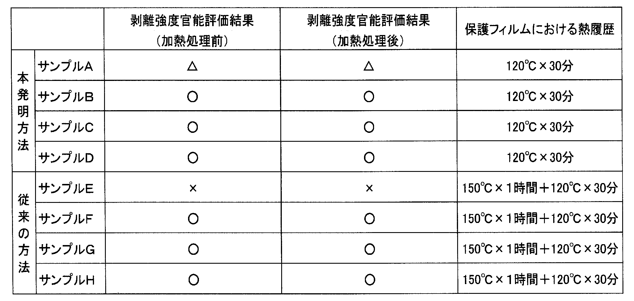
表4及び表5に示されるように、本発明の製造方法によって製造されたサンプルA~Dに係る透明導電フィルム積層体に関しては、加熱処理後の保護フィルム4の剥離強度が、いずれも6.5gf/cm以下であり、容易に剥離可能なものであることが分かる。これに対し、従来の製造方法により製造されたサンプルE~Hに係る透明導電フィルム積層体に関しては、サンプルF~Hについては、低い剥離強度を有する結果となったが、サンプルEについては、剥離強度が10.50gf/cmと高い結果となり、保護フィルム4を剥離しにくく、該保護フィルム4を剥離させた場合に透明導電層2(ITO膜)等に損傷を与える可能性が懸念されるものであることが分かる。ここで、上記表4及び表5の結果から、保護フィルム4の剥離時に透明導電層2(ITO膜)等に損傷を与えることが無い剥離強度の上限値としては、サンプルEの加熱処理後の測定結果である10.50gf/cmと、サンプルAの加熱処理前の測定結果である7.25gf/cmとの間の数値である9.0gf/cm近傍であると推測することができるため、透明導電フィルム積層体が備える保護フィルム4の剥離強度としては、9.0gf/cm以下に設定することが好ましいといえる。
上記のように、従来の製造方法を採用する場合、使用できる保護フィルム4としては、サンプルE~Hに係る4種類の保護フィルム4の内、サンプルF~Hの三種類であるのに対し、本発明に係る製造方法を採用する場合、サンプルA~Dの全てに係る4種類の保護フィルム4を使用することが可能となり、剥離特性という観点からも、使用できる保護フィルム4の選択肢の幅を拡げることができ、効率よく透明導電フィルム積層体(保護フィルム4付きの透明導電フィルム3)を製造することが可能となることが分かる。また、本発明に係る製造方法を採用する場合、保護フィルム4に与える熱負荷を軽減できる結果、従来の製造方法と比べて、保護フィルムが有する粘着剤層42の剥離強度が上昇することを抑制できていることが分かる。
1 透明フィルム
2 透明導電層
3 透明導電フィルム
4 保護フィルム
41 保護フィルム本体
42 粘着剤層
2 透明導電層
3 透明導電フィルム
4 保護フィルム
41 保護フィルム本体
42 粘着剤層
Claims (3)
- 透明フィルムの一方面に透明導電層を成膜し、透明導電フィルムを形成する透明導電フィルム形成ステップと、
前記透明導電フィルムを少なくとも135℃の温度で少なくとも0.2時間加熱処理を行う加熱処理ステップと、
前記透明フィルムの他方面を保護し、剥離可能な保護フィルムを貼り合わせる保護フィルム積層ステップとを備え、
前記保護フィルム積層ステップは、前記加熱処理ステップ後に実施されることを特徴とする透明導電フィルム積層体の製造方法。 - 前記透明導電フィルム形成ステップは、少なくとも180℃以下のスパッタリング法により透明フィルムの一方面に前記透明導電層を形成する工程を備えることを特徴とする請求項1に記載の透明導電フィルム積層体の製造方法。
- 前記加熱処理ステップは、前記透明導電層を結晶化処理する工程である請求項1又は2に記載の透明導電フィルム積層体の製造方法。
Priority Applications (1)
| Application Number | Priority Date | Filing Date | Title |
|---|---|---|---|
| JP2020527490A JP6963159B2 (ja) | 2018-06-28 | 2019-06-22 | 透明導電フィルム積層体の製造方法 |
Applications Claiming Priority (2)
| Application Number | Priority Date | Filing Date | Title |
|---|---|---|---|
| JP2018122674 | 2018-06-28 | ||
| JP2018-122674 | 2018-06-28 |
Publications (1)
| Publication Number | Publication Date |
|---|---|
| WO2020004289A1 true WO2020004289A1 (ja) | 2020-01-02 |
Family
ID=68986915
Family Applications (1)
| Application Number | Title | Priority Date | Filing Date |
|---|---|---|---|
| PCT/JP2019/024849 Ceased WO2020004289A1 (ja) | 2018-06-28 | 2019-06-22 | 透明導電フィルム積層体の製造方法 |
Country Status (2)
| Country | Link |
|---|---|
| JP (1) | JP6963159B2 (ja) |
| WO (1) | WO2020004289A1 (ja) |
Citations (2)
| Publication number | Priority date | Publication date | Assignee | Title |
|---|---|---|---|---|
| JP2016030374A (ja) * | 2014-07-28 | 2016-03-07 | 日東電工株式会社 | 透明導電性積層体およびその製造方法、透明導電性フィルムの製造方法、ならびに透明導電性フィルム巻回体の製造方法 |
| JP2016056423A (ja) * | 2014-09-11 | 2016-04-21 | 凸版印刷株式会社 | パターン化透明導電性フィルムの製造方法およびパターン化透明導電性フィルム |
-
2019
- 2019-06-22 JP JP2020527490A patent/JP6963159B2/ja active Active
- 2019-06-22 WO PCT/JP2019/024849 patent/WO2020004289A1/ja not_active Ceased
Patent Citations (2)
| Publication number | Priority date | Publication date | Assignee | Title |
|---|---|---|---|---|
| JP2016030374A (ja) * | 2014-07-28 | 2016-03-07 | 日東電工株式会社 | 透明導電性積層体およびその製造方法、透明導電性フィルムの製造方法、ならびに透明導電性フィルム巻回体の製造方法 |
| JP2016056423A (ja) * | 2014-09-11 | 2016-04-21 | 凸版印刷株式会社 | パターン化透明導電性フィルムの製造方法およびパターン化透明導電性フィルム |
Also Published As
| Publication number | Publication date |
|---|---|
| JP6963159B2 (ja) | 2021-11-05 |
| JPWO2020004289A1 (ja) | 2021-06-03 |
Similar Documents
| Publication | Publication Date | Title |
|---|---|---|
| JP6600550B2 (ja) | 金属層積層透明導電性フィルムおよびそれを用いたタッチセンサ | |
| CN107705883B (zh) | 透明电极、包括其的触摸传感器及影像显示装置 | |
| US20110291968A1 (en) | Transparent electrically conductive substrate | |
| CN107000409A (zh) | 透明导电性膜层叠体及其用途 | |
| JP6553451B2 (ja) | 透明樹脂フィルム、透明導電性フィルムおよびそれを用いたタッチパネル | |
| KR20130031910A (ko) | 점착제층이 형성된 수지 필름, 적층 필름 및 터치 패널 | |
| CN107533402B (zh) | 透明导电体及其制造方法以及触摸面板 | |
| CN107408421B (zh) | 透明导电体和触摸面板 | |
| CN104704456A (zh) | 图案化膜和方法 | |
| CN108602315A (zh) | 导电性层叠薄膜 | |
| TWI674521B (zh) | 製造薄膜觸控感知器方法及裝置 | |
| CN107206769A (zh) | 导电膜层叠体 | |
| TW202213393A (zh) | 透明導電性薄膜 | |
| CN116367996A (zh) | 透明导电性薄膜 | |
| CN105590662B (zh) | 透明导电体以及触摸屏 | |
| JP6390395B2 (ja) | 透明導電体及びタッチパネル | |
| CN105103098A (zh) | 触控面板、其制备方法以及用于触控面板的银-钯-钕合金 | |
| JP6963159B2 (ja) | 透明導電フィルム積層体の製造方法 | |
| JP2016134320A (ja) | 透明導電体及びタッチパネル | |
| KR101865687B1 (ko) | 필름 터치 센서 제조 방법 및 제조 장치 | |
| CN110088714A (zh) | 带载体薄膜的透明导电性薄膜及使用其的触摸面板 | |
| JP6364285B2 (ja) | 透明電極用フィルム | |
| JP2016091299A (ja) | タッチパネル及びその製造方法 | |
| TWI609301B (zh) | Laminated body and stack manufacturing method for manufacturing electronic parts, film sensor, touch panel device with thin film sensor, and film forming method for forming metal layer with concentration gradient | |
| KR101834870B1 (ko) | 투명 전극 및 이를 포함하는 터치 센서 |
Legal Events
| Date | Code | Title | Description |
|---|---|---|---|
| 121 | Ep: the epo has been informed by wipo that ep was designated in this application |
Ref document number: 19827095 Country of ref document: EP Kind code of ref document: A1 |
|
| ENP | Entry into the national phase |
Ref document number: 2020527490 Country of ref document: JP Kind code of ref document: A |
|
| NENP | Non-entry into the national phase |
Ref country code: DE |
|
| 122 | Ep: pct application non-entry in european phase |
Ref document number: 19827095 Country of ref document: EP Kind code of ref document: A1 |