WO2020003972A1 - 固体撮像装置及び電子機器 - Google Patents
固体撮像装置及び電子機器 Download PDFInfo
- Publication number
- WO2020003972A1 WO2020003972A1 PCT/JP2019/022699 JP2019022699W WO2020003972A1 WO 2020003972 A1 WO2020003972 A1 WO 2020003972A1 JP 2019022699 W JP2019022699 W JP 2019022699W WO 2020003972 A1 WO2020003972 A1 WO 2020003972A1
- Authority
- WO
- WIPO (PCT)
- Prior art keywords
- pixel
- solid
- imaging device
- state imaging
- light
- Prior art date
- Legal status (The legal status is an assumption and is not a legal conclusion. Google has not performed a legal analysis and makes no representation as to the accuracy of the status listed.)
- Ceased
Links
Images








Classifications
-
- H—ELECTRICITY
- H10—SEMICONDUCTOR DEVICES; ELECTRIC SOLID-STATE DEVICES NOT OTHERWISE PROVIDED FOR
- H10F—INORGANIC SEMICONDUCTOR DEVICES SENSITIVE TO INFRARED RADIATION, LIGHT, ELECTROMAGNETIC RADIATION OF SHORTER WAVELENGTH OR CORPUSCULAR RADIATION
- H10F30/00—Individual radiation-sensitive semiconductor devices in which radiation controls the flow of current through the devices, e.g. photodetectors
- H10F30/20—Individual radiation-sensitive semiconductor devices in which radiation controls the flow of current through the devices, e.g. photodetectors the devices having potential barriers, e.g. phototransistors
- H10F30/21—Individual radiation-sensitive semiconductor devices in which radiation controls the flow of current through the devices, e.g. photodetectors the devices having potential barriers, e.g. phototransistors the devices being sensitive to infrared, visible or ultraviolet radiation
- H10F30/22—Individual radiation-sensitive semiconductor devices in which radiation controls the flow of current through the devices, e.g. photodetectors the devices having potential barriers, e.g. phototransistors the devices being sensitive to infrared, visible or ultraviolet radiation the devices having only one potential barrier, e.g. photodiodes
- H10F30/225—Individual radiation-sensitive semiconductor devices in which radiation controls the flow of current through the devices, e.g. photodetectors the devices having potential barriers, e.g. phototransistors the devices being sensitive to infrared, visible or ultraviolet radiation the devices having only one potential barrier, e.g. photodiodes the potential barrier working in avalanche mode, e.g. avalanche photodiodes
-
- H—ELECTRICITY
- H10—SEMICONDUCTOR DEVICES; ELECTRIC SOLID-STATE DEVICES NOT OTHERWISE PROVIDED FOR
- H10F—INORGANIC SEMICONDUCTOR DEVICES SENSITIVE TO INFRARED RADIATION, LIGHT, ELECTROMAGNETIC RADIATION OF SHORTER WAVELENGTH OR CORPUSCULAR RADIATION
- H10F39/00—Integrated devices, or assemblies of multiple devices, comprising at least one element covered by group H10F30/00, e.g. radiation detectors comprising photodiode arrays
- H10F39/80—Constructional details of image sensors
- H10F39/802—Geometry or disposition of elements in pixels, e.g. address-lines or gate electrodes
- H10F39/8023—Disposition of the elements in pixels, e.g. smaller elements in the centre of the imager compared to larger elements at the periphery
-
- H—ELECTRICITY
- H10—SEMICONDUCTOR DEVICES; ELECTRIC SOLID-STATE DEVICES NOT OTHERWISE PROVIDED FOR
- H10F—INORGANIC SEMICONDUCTOR DEVICES SENSITIVE TO INFRARED RADIATION, LIGHT, ELECTROMAGNETIC RADIATION OF SHORTER WAVELENGTH OR CORPUSCULAR RADIATION
- H10F39/00—Integrated devices, or assemblies of multiple devices, comprising at least one element covered by group H10F30/00, e.g. radiation detectors comprising photodiode arrays
- H10F39/80—Constructional details of image sensors
- H10F39/802—Geometry or disposition of elements in pixels, e.g. address-lines or gate electrodes
- H10F39/8027—Geometry of the photosensitive area
-
- H—ELECTRICITY
- H10—SEMICONDUCTOR DEVICES; ELECTRIC SOLID-STATE DEVICES NOT OTHERWISE PROVIDED FOR
- H10F—INORGANIC SEMICONDUCTOR DEVICES SENSITIVE TO INFRARED RADIATION, LIGHT, ELECTROMAGNETIC RADIATION OF SHORTER WAVELENGTH OR CORPUSCULAR RADIATION
- H10F39/00—Integrated devices, or assemblies of multiple devices, comprising at least one element covered by group H10F30/00, e.g. radiation detectors comprising photodiode arrays
- H10F39/80—Constructional details of image sensors
- H10F39/803—Pixels having integrated switching, control, storage or amplification elements
-
- H—ELECTRICITY
- H10—SEMICONDUCTOR DEVICES; ELECTRIC SOLID-STATE DEVICES NOT OTHERWISE PROVIDED FOR
- H10F—INORGANIC SEMICONDUCTOR DEVICES SENSITIVE TO INFRARED RADIATION, LIGHT, ELECTROMAGNETIC RADIATION OF SHORTER WAVELENGTH OR CORPUSCULAR RADIATION
- H10F39/00—Integrated devices, or assemblies of multiple devices, comprising at least one element covered by group H10F30/00, e.g. radiation detectors comprising photodiode arrays
- H10F39/80—Constructional details of image sensors
- H10F39/805—Coatings
- H10F39/8057—Optical shielding
-
- H—ELECTRICITY
- H10—SEMICONDUCTOR DEVICES; ELECTRIC SOLID-STATE DEVICES NOT OTHERWISE PROVIDED FOR
- H10F—INORGANIC SEMICONDUCTOR DEVICES SENSITIVE TO INFRARED RADIATION, LIGHT, ELECTROMAGNETIC RADIATION OF SHORTER WAVELENGTH OR CORPUSCULAR RADIATION
- H10F39/00—Integrated devices, or assemblies of multiple devices, comprising at least one element covered by group H10F30/00, e.g. radiation detectors comprising photodiode arrays
- H10F39/80—Constructional details of image sensors
- H10F39/806—Optical elements or arrangements associated with the image sensors
-
- H—ELECTRICITY
- H10—SEMICONDUCTOR DEVICES; ELECTRIC SOLID-STATE DEVICES NOT OTHERWISE PROVIDED FOR
- H10F—INORGANIC SEMICONDUCTOR DEVICES SENSITIVE TO INFRARED RADIATION, LIGHT, ELECTROMAGNETIC RADIATION OF SHORTER WAVELENGTH OR CORPUSCULAR RADIATION
- H10F39/00—Integrated devices, or assemblies of multiple devices, comprising at least one element covered by group H10F30/00, e.g. radiation detectors comprising photodiode arrays
- H10F39/80—Constructional details of image sensors
- H10F39/806—Optical elements or arrangements associated with the image sensors
- H10F39/8063—Microlenses
-
- H—ELECTRICITY
- H10—SEMICONDUCTOR DEVICES; ELECTRIC SOLID-STATE DEVICES NOT OTHERWISE PROVIDED FOR
- H10F—INORGANIC SEMICONDUCTOR DEVICES SENSITIVE TO INFRARED RADIATION, LIGHT, ELECTROMAGNETIC RADIATION OF SHORTER WAVELENGTH OR CORPUSCULAR RADIATION
- H10F39/00—Integrated devices, or assemblies of multiple devices, comprising at least one element covered by group H10F30/00, e.g. radiation detectors comprising photodiode arrays
- H10F39/80—Constructional details of image sensors
- H10F39/807—Pixel isolation structures
-
- H—ELECTRICITY
- H10—SEMICONDUCTOR DEVICES; ELECTRIC SOLID-STATE DEVICES NOT OTHERWISE PROVIDED FOR
- H10F—INORGANIC SEMICONDUCTOR DEVICES SENSITIVE TO INFRARED RADIATION, LIGHT, ELECTROMAGNETIC RADIATION OF SHORTER WAVELENGTH OR CORPUSCULAR RADIATION
- H10F77/00—Constructional details of devices covered by this subclass
- H10F77/30—Coatings
- H10F77/306—Coatings for devices having potential barriers
- H10F77/331—Coatings for devices having potential barriers for filtering or shielding light, e.g. multicolour filters for photodetectors
- H10F77/334—Coatings for devices having potential barriers for filtering or shielding light, e.g. multicolour filters for photodetectors for shielding light, e.g. light blocking layers or cold shields for infrared detectors
-
- H—ELECTRICITY
- H10—SEMICONDUCTOR DEVICES; ELECTRIC SOLID-STATE DEVICES NOT OTHERWISE PROVIDED FOR
- H10F—INORGANIC SEMICONDUCTOR DEVICES SENSITIVE TO INFRARED RADIATION, LIGHT, ELECTROMAGNETIC RADIATION OF SHORTER WAVELENGTH OR CORPUSCULAR RADIATION
- H10F77/00—Constructional details of devices covered by this subclass
- H10F77/40—Optical elements or arrangements
- H10F77/407—Optical elements or arrangements indirectly associated with the devices
Definitions
- the present disclosure relates to a solid-state imaging device and an electronic device.
- Patent Document 1 describes a photoelectric conversion element in which the light receiving area of a first pixel is different from the light receiving area of a second pixel.
- the SPAD photodiode when the amount of incident light is large, such as when capturing an image of a high-luminance subject, the relationship between the amount of light and the received light signal changes compared to when the amount of light is small. In such a case, there is a problem that the distance of the subject cannot be measured accurately.
- the SPAD photodiode it has been desired for the SPAD photodiode to accurately capture a subject regardless of a long distance or a short distance.
- a pixel separation unit that defines a photoelectric conversion region for each pixel, a first semiconductor layer provided in the photoelectric conversion region, and a voltage for electron multiplication between the first semiconductor layer. And a second semiconductor layer to which a plurality of pixels are applied, and wherein the plurality of pixels have different sensitivities.
- a pixel separation unit that defines a photoelectric conversion region for each pixel, a first semiconductor layer provided in the photoelectric conversion region, and an electron multiplication between the first semiconductor layer. And a second semiconductor layer to which a voltage is applied, and wherein the plurality of pixels have different sensitivities in the photoelectric conversion regions, and are provided with a solid-state imaging device.
- a SPAD photodiode can accurately capture a subject regardless of a long distance or a short distance.
- the above effects are not necessarily limited, and any of the effects described in the present specification or other effects that can be grasped from the present specification, together with or instead of the above effects. May be played.
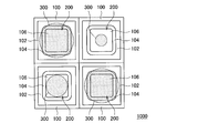
- FIG. 1 is a plan view illustrating a solid-state imaging device (SPAD photodiode) according to an embodiment of the present disclosure.
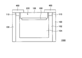
- FIG. 2 is a schematic cross-sectional view illustrating a configuration of one pixel of the solid-state imaging device.
- FIG. 2 is a plan view showing a solid-state image sensor similar to FIG. 1, showing an example including a plurality of sizes of condenser lenses.
- FIG. 4 is a plan view illustrating an example in which a pixel without a condenser lens is provided.
- FIG. 3 is a plan view illustrating an example in which a plurality of condenser lenses are provided for one pixel.
- FIG. 9 is a schematic diagram illustrating an example in which sensitivity is adjusted for each pixel by changing the width of a light-shielding film for each pixel.
- FIG. 9 is a schematic diagram illustrating an example in which sensitivity is adjusted for each pixel by changing the width of a light-shielding film for each pixel.
- FIG. 3 is a schematic cross-sectional view illustrating a configuration of a light shielding film of three pixels.
- FIG. 3 is a plan view illustrating a solid-state imaging device, and is a diagram illustrating an example in which a plurality of types of light-shielding films having different light-shielding widths are provided in three of four pixels.
- FIG. 12 is a schematic cross-sectional view illustrating a detailed configuration of a photoelectric conversion unit with respect to the configuration illustrated in FIG. 11.
- FIG. 21 is a block diagram illustrating a configuration example of a camera device as an electronic device to which the present technology is applied.
- Configuration example of solid-state imaging device according to present embodiment 1.1.
- Configuration example of solid-state imaging device 1.1.
- Example of Basic Configuration of Solid-State Imaging Device There is a technology of SPAD (Single Photon Avalanche Diode) that realizes a photodiode having readout sensitivity of one photon level by performing electron multiplication.
- SPAD Single Photon Avalanche Diode
- a high voltage of about ⁇ several tens of volts is used to cause multiplication.
- SPAD is a device capable of detecting one photon for each pixel by multiplying carriers generated by photoelectric conversion in a PN junction region of a high electric field provided for each pixel.
- FIG. 1 is a plan view showing a solid-state imaging device (SPAD photodiode; solid-state imaging device) 1000 according to an embodiment of the present disclosure.
- FIG. 1 shows four pixels included in the solid-state imaging device 1000.
- FIG. 2 is a schematic cross-sectional view showing the configuration of one pixel of the solid-state imaging device 1000.
- the sensitivity is controlled only by changing the upper layer layout without changing the lower layer layout by changing the lens size, shape, and light blocking width of the condensing portion of the upper layer, while the cell size of the lower layer is the same.
- each pixel of the solid-state imaging device 1000 is partitioned by the element separating unit 100, and the photoelectric conversion unit 200 is configured for each pixel.
- the element isolation section 100 is made of, for example, an insulating film or a metal film.
- each pixel partitioned by the element isolation unit 100 is provided with a P-type layer 102 extending from the edge of the element isolation unit 100 to the bottom of each pixel.
- a mold layer 104 is provided.
- a high-concentration N-type layer 106 is provided on the light irradiation surface side (upper side in the drawing) of the photoelectric conversion unit 200, and a high-concentration P-type layer 108 is provided below the high-concentration N-type layer 106. Have been.
- a high-concentration P-type layer 110 is provided above the P-type layer 102 formed along the element isolation part 100. As an example, a high voltage is applied between the P-type layer 108 and the N-type layer 104 to cause the above-described electron multiplication.
- the conductivity type of the impurity layer is merely an example, and P and N may be exchanged to have the opposite conductivity type.
- a multiplication region in which a high electric field is generated.
- an impurity implantation region for separating the multiplication region may be provided, or STI (Sallow Trench Isolation) or the like may be provided as the pixel separation unit 150.
- Example in which the size of the condenser lens differs for each pixel Above the photoelectric conversion unit 200, a condenser lens 300 that collects light on the photoelectric conversion unit 200 is provided. As shown in FIG. 1, the condensing lens 300 is formed in a different size for each pixel.
- the size of the condenser lens 300 of the upper left pixel and the lower right pixel in the drawing is configured to be larger than the size of the condenser lens 300 of the lower left pixel and the upper right pixel. . Accordingly, the sensitivity at the time of performing the photoelectric conversion can be changed for each pixel according to the size of the condenser lens 300.
- the size of the condenser lens 300 of the upper left pixel and the lower right pixel is the same, and the size of the condenser lens 300 of the lower left pixel and the upper right pixel is the same.
- the position of the condenser lens 300 is arranged at the center of the pixel. However, the position of the condenser lens 300 is shifted from the center of the pixel according to the position of the pixel in the pixel area on the imaging surface. May be arranged. For example, for a pixel located at the upper right of the pixel area, the condenser lens 300 is disposed at the lower left with respect to the center of the pixel. Thereby, the position of the condenser lens 300 can be optimally arranged according to the position of the pixel on the imaging surface.
- FIG. 3 is a plan view showing the solid-state imaging device 1000 similarly to FIG. 1, and is a diagram showing an example in which condensing lenses 300 of several sizes are provided.
- FIG. 4 is a plan view showing an example in which pixels without the condenser lens 300 are provided.
- FIG. 5 is a plan view showing an example in which a plurality of condenser lenses 300 are provided for one pixel. 3 to 5, the sensitivity at the time of performing the photoelectric conversion can be changed for each pixel according to the size of the condenser lens 300.
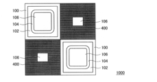
- FIGS. 6 and 7 are schematic diagrams illustrating an example in which the sensitivity is adjusted for each pixel by changing the width of the light-shielding film for each pixel.
- FIG. 6 is a plan view showing the solid-state imaging device 1000 as in FIG. 1, and shows four pixels included in the solid-state imaging device 1000.
- FIG. 6 the basic configuration of each pixel including the photoelectric conversion unit 200 is the same as in FIGS.
- a light shielding film 400 is provided in some pixels.
- FIG. 7 is a schematic cross-sectional view illustrating a configuration of a pixel provided with a light-shielding film 400.
- the light-blocking film 400 has a function of blocking a part of light incident on the photoelectric conversion unit 200. As described above, by providing the light-shielding film 400 in some of the pixels, the sensitivity can be adjusted for each pixel.
- a condenser lens 300 may be provided on the light shielding film 400.
- FIG. 8 is a schematic sectional view showing the configuration of the light shielding film 400 of three pixels.
- condensing lenses 300 are provided corresponding to the photoelectric conversion units 200 of each pixel.
- a light shielding film 400 is provided on the photoelectric conversion unit 200 of each pixel.
- Each pixel has the same cell size, but has a different width in a region blocked by the light-shielding film 400. Thereby, sensitivity adjustment can be performed for each pixel.
- FIG. 9 is a plan view showing the solid-state imaging device 1000, and shows an example in which a plurality of types of light-shielding films 400 having different light-shielding widths are provided in three of the four pixels. Thereby, sensitivity adjustment can be performed for each pixel.
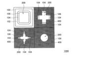
- FIG. 10 is a plan view showing variations in the shape of the opening of the light-shielding film 400.
- the shape of the opening of the light-shielding film 400 of the upper right and lower left pixels in the drawing is a cross shape. Further, the shape of the opening of the light shielding film 400 of the lower right pixel is circular.
- the shape of the opening of the light-shielding film 400 can be various shapes such as a rectangle, a polygon, and a circle.
- FIG. 11 is a schematic diagram illustrating an example in which the thickness of a transmission film 500 provided between the photoelectric conversion unit 200 and the condenser lens 300 is different. It is. Light emitted to the light irradiation surface of the photoelectric conversion unit 200 passes through the transmission film 500 and enters the photoelectric conversion unit 200.
- the permeable film 500 is composed of an insulating film. Further, the transmission film 500 may be formed of a metal film.
- FIG. 11 is a schematic sectional view showing the configuration of the transmission film 500 of three pixels.
- a condenser lens 300 is provided corresponding to the photoelectric conversion unit 200 of each pixel.
- the transmission film 500 is provided between the condenser lens 300 and the photoelectric conversion unit 200.
- FIG. 12 is a schematic cross-sectional view showing a detailed configuration of the photoelectric conversion unit 200 of each pixel with respect to the configuration shown in FIG.
- the detailed configuration of the photoelectric conversion unit 200 is the same as that shown in FIG. In FIG. 12, the illustration of the condenser lens 300 is omitted.
- the sensitivity can be adjusted for each pixel by making the thickness of the transmission film 500 different for each pixel.
- FIG. 13 is a block diagram illustrating a configuration example of a camera device 2000 as an electronic device to which the present technology is applied.
- a camera device 2000 illustrated in FIG. 20 includes an optical unit 2100 including a lens group, the above-described solid-state imaging device (imaging device) 1000, and a DSP circuit 2200 that is a camera signal processing device.
- the camera device 2000 also includes a frame memory 2300, a display unit (display device) 2400, a recording unit 2500, an operation unit 2600, and a power supply unit 2700.
- the DSP circuit 2200, the frame memory 2300, the display unit 2400, the recording unit 2500, the operation unit 2600, and the power supply unit 2700 are mutually connected via a bus line 2800.
- the optical unit 2100 captures incident light (image light) from a subject and forms an image on the imaging surface of the solid-state imaging device 1000.
- the solid-state imaging device 1000 converts the amount of incident light formed on the imaging surface by the optical unit 2100 into an electric signal for each pixel and outputs the electric signal as a pixel signal.
- the display unit 2400 includes a panel-type display device such as a liquid crystal panel or an organic EL (Electro Luminescence) panel, and displays a moving image or a still image captured by the solid-state imaging device 1000.
- the DSP circuit 2200 receives a pixel signal output from the solid-state imaging device 1000 and performs processing for displaying the pixel signal on the display unit 2400.
- the recording unit 2500 records a moving image or a still image captured by the solid-state imaging device 1000 on a recording medium such as a video tape or a DVD (Digital Versatile Disk).
- the operation unit 2600 issues operation commands for various functions of the solid-state imaging device 1000 under an operation by the user.
- the power supply unit 2700 appropriately supplies various power supplies serving as operation power supplies for the DSP circuit 2200, the frame memory 2300, the display unit 2400, the recording unit 2500, and the operation unit 2600 to these supply targets.
- pixels having different sensitivities can be realized only by changing the layout of the upper layer of the solid-state imaging device 1000, and the solid-state imaging device 1000 having a wide dynamic range can be realized. Becomes possible.
- a pixel separation unit that defines a photoelectric conversion region for each pixel, A first semiconductor layer provided in the photoelectric conversion region; A second semiconductor layer to which a voltage for electron multiplication is applied between the first semiconductor layer and the first semiconductor layer; With A solid-state imaging device, wherein a plurality of pixels have different sensitivities of the photoelectric conversion regions.
- the solid-state imaging device according to (2) further including the pixel without the condenser lens.
- a light-transmitting film that is provided on a light irradiation surface of the photoelectric conversion region for each of the pixels and transmits light reaching the light irradiation surface, The transmission film having a different thickness is provided for each of the pixels,
- a pixel separation unit that defines a photoelectric conversion region for each pixel, a first semiconductor layer provided in the photoelectric conversion region, and a second voltage to which a voltage for electron multiplication is applied between the first semiconductor layer and the second semiconductor layer.
- a semiconductor layer wherein the plurality of pixels are configured to have different sensitivities in the photoelectric conversion regions, the electronic device including a solid-state imaging device.
Landscapes
- Solid State Image Pick-Up Elements (AREA)
- Transforming Light Signals Into Electric Signals (AREA)
- Control Of Motors That Do Not Use Commutators (AREA)
- Light Receiving Elements (AREA)
Abstract
SPADフォトダイオードにおいて、遠距離、近距離に関わらず、被写体を正確に捉える。本開示に係る固体撮像装置(1000)は、光電変換領域(200)を画素毎に画定する画素分離部(100)と、前記光電変換領域に設けられた第1半導体層(106)と、前記第1半導体層との間に電子増倍のための電圧が印加される第2半導体層(108)と、を備え、複数の前記画素の感度が異なるように構成される。この構成により、SPADフォトダイオードにおいて、遠距離、近距離に関わらず、被写体を正確に捉えることが可能となる。
Description
本開示は、固体撮像装置及び電子機器に関する。
従来、下記の特許文献1には、第1のピクセルの受光面積と第2のピクセルの受光面積を異なるようにした光電変換素子が記載されている。
近時においては、画素毎に画定された光電変換領域に設けられた第1半導体層と第2半導体層との間に電子増倍のための電圧が印加される、いわゆるSPADフォトダイオードが知られている。
このSPADフォトダイオードでは、高輝度の被写体を撮像する場合など、入射する光量が多い場合は、光量が少ない場合に比べて、光量に対する受光信号の関係に変化が生じる。このような場合、被写体を正確に測距できなくなる問題が生じる。
より具体的には、SPADフォトダイオードにおける測距レンジ拡大において、遠距離までカバーするためには、高感度のSPADフォトダイオードを準備する必要がある。しかし、高感度のSPADフォトダイオードにおいて、入射する光量が多い場合は、光量が少ない場合に比べて光量に対する受光信号の関係に変化が生じるため、太陽光等の高照度の光に対して測距できない状況が発生する。
上記特許文献1に記載された技術では、画素を異なるサイズとすることで画素毎に感度を変えている。このような手法では、画素のセルサイズの変更という比較的大掛かりな構造の変更が必要であるため、設計変更に煩雑な手間がかかるとともに、製造コストの増大を招来する問題がある。
そこで、SPADフォトダイオードにおいて、遠距離、近距離に関わらず、被写体を正確に捉えることが望まれていた。
本開示によれば、光電変換領域を画素毎に画定する画素分離部と、前記光電変換領域に設けられた第1半導体層と、前記第1半導体層との間に電子増倍のための電圧が印加される第2半導体層と、を備え、複数の前記画素の感度が異なるように構成された、固体撮像装置が提供される。
また、本開示によれば、光電変換領域を画素毎に画定する画素分離部と、前記光電変換領域に設けられた第1半導体層と、前記第1半導体層との間に電子増倍のための電圧が印加される第2半導体層と、を有し、複数の前記画素の前記光電変換領域の感度が異なるように構成された、固体撮像装置を備える、電子機器が提供される。
また、本開示によれば、光電変換領域を画素毎に画定する画素分離部と、前記光電変換領域に設けられた第1半導体層と、前記第1半導体層との間に電子増倍のための電圧が印加される第2半導体層と、を有し、複数の前記画素の前記光電変換領域の感度が異なるように構成された、固体撮像装置を備える、電子機器が提供される。
本開示によれば、SPADフォトダイオードにおいて、遠距離、近距離に関わらず、被写体を正確に捉えることが可能となる。
なお、上記の効果は必ずしも限定的なものではなく、上記の効果とともに、または上記の効果に代えて、本明細書に示されたいずれかの効果、または本明細書から把握され得る他の効果が奏されてもよい。
なお、上記の効果は必ずしも限定的なものではなく、上記の効果とともに、または上記の効果に代えて、本明細書に示されたいずれかの効果、または本明細書から把握され得る他の効果が奏されてもよい。
以下に添付図面を参照しながら、本開示の好適な実施の形態について詳細に説明する。なお、本明細書及び図面において、実質的に同一の機能構成を有する構成要素については、同一の符号を付することにより重複説明を省略する。
なお、説明は以下の順序で行うものとする。
1.本実施形態に係る固体撮像素子の構成例
1.1.固体撮像素子の基本的構成例
1.2.画素毎に集光レンズの大きさを異ならせる例
1.3.画素毎に遮光膜の幅を異ならせる例
1.4.光電変換部と集光レンズ間の透過膜の膜厚を異ならせる例
2.本実施形態に係る固体撮像素子の適用例
1.本実施形態に係る固体撮像素子の構成例
1.1.固体撮像素子の基本的構成例
1.2.画素毎に集光レンズの大きさを異ならせる例
1.3.画素毎に遮光膜の幅を異ならせる例
1.4.光電変換部と集光レンズ間の透過膜の膜厚を異ならせる例
2.本実施形態に係る固体撮像素子の適用例
1.本実施形態に係る固体撮像素子の構成例
1.1.固体撮像素子の基本的構成例
電子増倍をすることにより1光子レベルの読み出し感度を持ったフォトダイオードを実現するSPAD(Single Photon Avalanche Diode)の技術がある。SPADでは、増倍を起こすために±数10V程度の高電圧が用いられる。SPADは、画素毎に設けられた高電界のPN接合領域で光電変換により発生したキャリアを増倍させることで、1個のフォトンを画素毎に検出することが可能なデバイスである。
1.1.固体撮像素子の基本的構成例
電子増倍をすることにより1光子レベルの読み出し感度を持ったフォトダイオードを実現するSPAD(Single Photon Avalanche Diode)の技術がある。SPADでは、増倍を起こすために±数10V程度の高電圧が用いられる。SPADは、画素毎に設けられた高電界のPN接合領域で光電変換により発生したキャリアを増倍させることで、1個のフォトンを画素毎に検出することが可能なデバイスである。
図1は本開示の一実施形態に係る固体撮像素子(SPADフォトダイオード;固体撮像装置)1000を示す平面図である。図1では、固体撮像素子1000が備える4つの画素を示している。また、図2は、固体撮像素子1000の1画素の構成を示す概略断面図である。本実施形態では、下層セルサイズは同じであるが上層の集光部分のレンズサイズや形状、遮光幅を変えることにより、下層レイアウトを変更することなく、上層レイアウトの変更だけで感度を制御する。
図1及び図2示すように、固体撮像素子1000の各画素は、素子分離部100によって区画され、各画素に光電変換部200が構成されている。素子分離部100は、一例として、絶縁膜または金属膜から構成される。図2に示すように、素子分離部100によって区画された各画素には、素子分離部100の縁から各画素の底部に延存するP型層102が設けられ、P型層102の内側にN型層104が設けられている。
また、光電変換部200の光照射面側(図面上で上側)には高濃度のN型層106が設けられ、高濃度のN型層106の下層には高濃度のP型層108が設けられている。また、素子分離部100に沿って形成されたP型層102の上部には、高濃度のP型層110が設けられている。一例として、上述した電子増倍を起こすため、P型層108とN型層104との間に高電圧が印加される。なお、不純物層の導電型は一例であり、PとNを入れ替えて逆の導電型にしても良い。また、高電界になる増倍領域の作り方は他にも様々な方法が考えられる。更に、増倍領域を分離するための不純物注入領域を設けたり、画素分離部150としてSTI(Sallow Trench Isolation)などを設けても良い。
1.2.画素毎に集光レンズの大きさを異ならせる例
光電変換部200の上部には、光電変換部200に光を集光させる集光レンズ300が設けられている。図1に示すように、集光レンズ300は、画素毎に異なるサイズで形成されている。
光電変換部200の上部には、光電変換部200に光を集光させる集光レンズ300が設けられている。図1に示すように、集光レンズ300は、画素毎に異なるサイズで形成されている。
図1に示す例では、図面上で左上の画素と右下の画素の集光レンズ300の大きさは、左下の画素と右上の画素の集光レンズ300のよりも大きいサイズで構成されている。これにより、集光レンズ300の大きさに応じて、光電変換を行う際の感度を画素毎に変更することができる。なお、図1に示す例では、左上の画素と右下の画素の集光レンズ300の大きさは同一であり、左下の画素と右上の画素の集光レンズ300の大きさは同一である。
図1に示す例では、集光レンズ300の位置を画素の中心に配置しているが、撮像面の画素領域における画素の位置に応じて、集光レンズ300の位置を画素の中心からずらすように配置しても良い。例えば、画素領域の右上に位置する画素では、画素の中心に対して左下に集光レンズ300を配置する。これにより、撮像面における画素の位置に応じて、集光レンズ300の位置を最適に配置できる。
図3は、図1と同様に固体撮像素子1000を示す平面図であって、数種類のサイズの集光レンズ300を備えた例を示す図である。また、図4は、集光レンズ300を備えていない画素を設けた例を示す平面図である。また、図5は、1の画素に複数の集光レンズ300を設けた例を示す平面図である。図3~図5の例においても、集光レンズ300の大きさに応じて、光電変換を行う際の感度を画素毎に変更することができる。
図4に示すように、集光レンズ300を備えていない画素を設けることで、集光レンズ300を設けた画素に対して、より広い感度差を実現できる。また、図5に示すように、1の画素に複数の集光レンズ300を設けることで、集光効率を高めることができる。また、複数の集光レンズ300の個数を調整することで、感度を容易に調整することが可能となる。以上のように、図3~図5に示す例においても、画素毎に感度調整を行うことができる。
1.3.画素毎に遮光膜の幅を異ならせる例
図6及び図7は、画素毎に遮光膜の幅を変えることで、画素毎に感度調整を行う例を示す模式図である。図6は、図1と同様に固体撮像素子1000を示す平面図であって、固体撮像素子1000が備える4つの画素を示している。
図6及び図7は、画素毎に遮光膜の幅を変えることで、画素毎に感度調整を行う例を示す模式図である。図6は、図1と同様に固体撮像素子1000を示す平面図であって、固体撮像素子1000が備える4つの画素を示している。
図6において、光電変換部200を含む各画素の基本的な構成は、図1及び図2と同様である。図6では、一部の画素に遮光膜400が設けられている。図7は、遮光膜400が設けられた画素の構成を示す概略断面図である。遮光膜400は、光電変換部200に入射する光の一部を遮光する機能を有する。このように、一部の画素に遮光膜400を設けることで、画素毎に感度調整を行うことが可能である。なお、図7において、遮光膜400の上に集光レンズ300が設けられていても良い。
図8は、3つの画素の遮光膜400の構成を示す概略断面図である。図8に示すように、各画素の光電変換部200に対応して集光レンズ300がそれぞれ設けられている。また、各画素の光電変換部200の上には、遮光膜400が設けられている。各画素は同じセルサイズであるが、遮光膜400によって遮られた領域の幅が異なる。これにより、画素毎に感度調整を行うことができる。
同様に、図9は、固体撮像素子1000を示す平面図であって、4つの画素のうちの3画素に複数種類の異なる遮光幅の遮光膜400を設けた例を示す図である。これにより、画素毎に感度調整を行うことができる。
図10は、遮光膜400の開口の形状のバリエーションを示す平面図である。図10では、図面上で右上と左下の画素の遮光膜400の開口の形状を十字形状としている。また、右下の画素の遮光膜400の開口の形状を円形としている。遮光膜400の開口の形状は、矩形、多角形、円形等、様々な形状とすることができる。
1.4.光電変換部と集光レンズ間の透過膜の膜厚を異ならせる例
図11は、光電変換部200と集光レンズ300の間に設けられる透過膜500の膜厚を異ならせる例を示す模式図である。光電変換部200の光照射面に照射される光は、透過膜500を透過して光電変換部200に入射する。透過膜500は、絶縁膜から構成される。また、透過膜500を金属膜から構成しても良い。
図11は、光電変換部200と集光レンズ300の間に設けられる透過膜500の膜厚を異ならせる例を示す模式図である。光電変換部200の光照射面に照射される光は、透過膜500を透過して光電変換部200に入射する。透過膜500は、絶縁膜から構成される。また、透過膜500を金属膜から構成しても良い。
図11は、3つの画素の透過膜500の構成を示す概略断面図である。図11に示すように、各画素の光電変換部200に対応して集光レンズ300がそれぞれ設けられている。各画素において、透過膜500は、集光レンズ300と光電変換部200との間に設けられている。
図11に示すように、中央の画素の透過膜500の膜厚は、その両側の画素の透過膜500よりも薄く形成されている。図12は、図11に示す構成に対し、各画素の光電変換部200の詳細な構成を示した概略断面図である。光電変換部200の詳細な構成は、図2に示したものと同様である。なお、図12において、集光レンズ300の図示は省略している。このように、画素毎に透過膜500の膜厚を異ならせることで、画素毎に感度調整を行うことができる。
2.本実施形態に係る固体撮像素子の適用例
図13は、本技術を適用した電子機器としての、カメラ装置2000の構成例を示すブロック図である。図20に示すカメラ装置2000は、レンズ群などからなる光学部2100、上述した固体撮像装置(撮像デバイス)1000、およびカメラ信号処理装置であるDSP回路2200を備える。また、カメラ装置2000は、フレームメモリ2300、表示部(表示装置)2400、記録部2500、操作部2600、および電源部2700も備える。DSP回路2200、フレームメモリ2300、表示部2400、記録部2500、操作部2600および電源部2700は、バスライン2800を介して相互に接続されている。
図13は、本技術を適用した電子機器としての、カメラ装置2000の構成例を示すブロック図である。図20に示すカメラ装置2000は、レンズ群などからなる光学部2100、上述した固体撮像装置(撮像デバイス)1000、およびカメラ信号処理装置であるDSP回路2200を備える。また、カメラ装置2000は、フレームメモリ2300、表示部(表示装置)2400、記録部2500、操作部2600、および電源部2700も備える。DSP回路2200、フレームメモリ2300、表示部2400、記録部2500、操作部2600および電源部2700は、バスライン2800を介して相互に接続されている。
光学部2100は、被写体からの入射光(像光)を取り込んで固体撮像装置1000の撮像面上に結像する。固体撮像装置1000は、光学部2100によって撮像面上に結像された入射光の光量を画素単位で電気信号に変換して画素信号として出力する。
表示部2400は、例えば、液晶パネルや有機EL(Electro Luminescence)パネル等のパネル型表示装置からなり、固体撮像装置1000で撮像された動画または静止画を表示する。DSP回路2200は、固体撮像装置1000から出力された画素信号を受け取り、表示部2400に表示させるための処理を行う。記録部2500は、固体撮像装置1000で撮像された動画または静止画を、ビデオテープやDVD(Digital Versatile Disk)等の記録媒体に記録する。
操作部2600は、ユーザによる操作の下に、固体撮像装置1000が有する様々な機能について操作指令を発する。電源部2700は、DSP回路2200、フレームメモリ2300、表示部2400、記録部2500および操作部2600の動作電源となる各種の電源を、これら供給対象に対して適宜供給する。
以上説明したように本実施形態によれば、固体撮像装置1000の上層のレイアウトを変更するのみで、異なる感度を有する画素を実現することができ、広いダイナミックレンジの固体撮像素子1000を実現することが可能となる。
以上、添付図面を参照しながら本開示の好適な実施形態について詳細に説明したが、本開示の技術的範囲はかかる例に限定されない。本開示の技術分野における通常の知識を有する者であれば、特許請求の範囲に記載された技術的思想の範疇内において、各種の変更例または修正例に想到し得ることは明らかであり、これらについても、当然に本開示の技術的範囲に属するものと了解される。
また、本明細書に記載された効果は、あくまで説明的または例示的なものであって限定的ではない。つまり、本開示に係る技術は、上記の効果とともに、または上記の効果に代えて、本明細書の記載から当業者には明らかな他の効果を奏しうる。
なお、以下のような構成も本開示の技術的範囲に属する。
(1)
光電変換領域を画素毎に画定する画素分離部と、
前記光電変換領域に設けられた第1半導体層と、
前記第1半導体層との間に電子増倍のための電圧が印加される第2半導体層と、
を備え、
複数の前記画素の前記光電変換領域の感度が異なるように構成された、固体撮像装置。
(2)
前記画素毎に光照射面に設けられた集光レンズを備え、
画素毎に異なる大きさの前記集光レンズが設けられた、
前記(1)に記載の固体撮像装置。
(3)
前記集光レンズを備えていない前記画素を有する、前記(2)に記載の固体撮像装置。
(4)
1画素に複数の前記集光レンズが設けられた、前記(2)に記載の固体撮像装置。
(5)
前記画素毎に前記光電変換領域の光照射面に到達する光を遮光する遮光部を備え、
前記画素毎に前記遮光部の遮光幅が異なる、
前記(1)に記載の固体撮像装置。
(6)
前記遮光部の開口の形状は、多角形又は円形である、前記(5)に記載の固体撮像装置。
(7)
前記画素毎に前記光電変換領域の光照射面に設けられ、光照射面に到達する光を透過する透過膜を備え、
前記画素毎に厚さの異なる前記透過膜が設けられた、
前記(1)に記載の固体撮像装置。
(8)
光電変換領域を画素毎に画定する画素分離部と、前記光電変換領域に設けられた第1半導体層と、前記第1半導体層との間に電子増倍のための電圧が印加される第2半導体層と、を有し、複数の前記画素の前記光電変換領域の感度が異なるように構成された、固体撮像装置を備える、電子機器。
(1)
光電変換領域を画素毎に画定する画素分離部と、
前記光電変換領域に設けられた第1半導体層と、
前記第1半導体層との間に電子増倍のための電圧が印加される第2半導体層と、
を備え、
複数の前記画素の前記光電変換領域の感度が異なるように構成された、固体撮像装置。
(2)
前記画素毎に光照射面に設けられた集光レンズを備え、
画素毎に異なる大きさの前記集光レンズが設けられた、
前記(1)に記載の固体撮像装置。
(3)
前記集光レンズを備えていない前記画素を有する、前記(2)に記載の固体撮像装置。
(4)
1画素に複数の前記集光レンズが設けられた、前記(2)に記載の固体撮像装置。
(5)
前記画素毎に前記光電変換領域の光照射面に到達する光を遮光する遮光部を備え、
前記画素毎に前記遮光部の遮光幅が異なる、
前記(1)に記載の固体撮像装置。
(6)
前記遮光部の開口の形状は、多角形又は円形である、前記(5)に記載の固体撮像装置。
(7)
前記画素毎に前記光電変換領域の光照射面に設けられ、光照射面に到達する光を透過する透過膜を備え、
前記画素毎に厚さの異なる前記透過膜が設けられた、
前記(1)に記載の固体撮像装置。
(8)
光電変換領域を画素毎に画定する画素分離部と、前記光電変換領域に設けられた第1半導体層と、前記第1半導体層との間に電子増倍のための電圧が印加される第2半導体層と、を有し、複数の前記画素の前記光電変換領域の感度が異なるように構成された、固体撮像装置を備える、電子機器。
300 集光レンズ
400 遮光膜
500 透過膜
1000 固体撮像素子
400 遮光膜
500 透過膜
1000 固体撮像素子
Claims (8)
- 光電変換領域を画素毎に画定する画素分離部と、
前記光電変換領域に設けられた第1半導体層と、
前記第1半導体層との間に電子増倍のための電圧が印加される第2半導体層と、
を備え、
複数の前記画素の前記光電変換領域の感度が異なるように構成された、固体撮像装置。 - 前記画素毎に光照射面に設けられた集光レンズを備え、
画素毎に異なる大きさの前記集光レンズが設けられた、
請求項1に記載の固体撮像装置。 - 前記集光レンズを備えていない前記画素を有する、請求項2に記載の固体撮像装置。
- 1画素に複数の前記集光レンズが設けられた、請求項2に記載の固体撮像装置。
- 前記画素毎に前記光電変換領域の光照射面に到達する光を遮光する遮光部を備え、
前記画素毎に前記遮光部の遮光幅が異なる、
請求項1に記載の固体撮像装置。 - 前記遮光部の開口の形状は、多角形又は円形である、請求項5に記載の固体撮像装置。
- 前記画素毎に前記光電変換領域の光照射面に設けられ、光照射面に到達する光を透過する透過膜を備え、
前記画素毎に厚さの異なる前記透過膜が設けられた、
請求項1に記載の固体撮像装置。 - 光電変換領域を画素毎に画定する画素分離部と、前記光電変換領域に設けられた第1半導体層と、前記第1半導体層との間に電子増倍のための電圧が印加される第2半導体層と、を有し、複数の前記画素の前記光電変換領域の感度が異なるように構成された、固体撮像装置を備える、電子機器。
Priority Applications (2)
| Application Number | Priority Date | Filing Date | Title |
|---|---|---|---|
| DE112019003237.2T DE112019003237T5 (de) | 2018-06-25 | 2019-06-07 | Festkörperbildaufnahmeeinrichtung und elektronische einrichtung |
| US17/252,810 US20210280622A1 (en) | 2018-06-25 | 2019-06-07 | Solid-state imaging apparatus and electronic apparatus |
Applications Claiming Priority (2)
| Application Number | Priority Date | Filing Date | Title |
|---|---|---|---|
| JP2018119768A JP2021158128A (ja) | 2018-06-25 | 2018-06-25 | 固体撮像装置及び電子機器 |
| JP2018-119768 | 2018-06-25 |
Publications (1)
| Publication Number | Publication Date |
|---|---|
| WO2020003972A1 true WO2020003972A1 (ja) | 2020-01-02 |
Family
ID=68968446
Family Applications (1)
| Application Number | Title | Priority Date | Filing Date |
|---|---|---|---|
| PCT/JP2019/022699 Ceased WO2020003972A1 (ja) | 2018-06-25 | 2019-06-07 | 固体撮像装置及び電子機器 |
Country Status (6)
| Country | Link |
|---|---|
| US (1) | US20210280622A1 (ja) |
| JP (1) | JP2021158128A (ja) |
| CN (2) | CN110634894A (ja) |
| DE (1) | DE112019003237T5 (ja) |
| TW (1) | TWI820154B (ja) |
| WO (1) | WO2020003972A1 (ja) |
Cited By (2)
| Publication number | Priority date | Publication date | Assignee | Title |
|---|---|---|---|---|
| WO2022024550A1 (ja) * | 2020-07-29 | 2022-02-03 | ソニーセミコンダクタソリューションズ株式会社 | 固体撮像装置及び電子機器 |
| JP2022107240A (ja) * | 2021-01-08 | 2022-07-21 | 株式会社東芝 | 光検出器、光検出システム、ライダー装置、移動体及び車 |
Families Citing this family (4)
| Publication number | Priority date | Publication date | Assignee | Title |
|---|---|---|---|---|
| JP2021158128A (ja) * | 2018-06-25 | 2021-10-07 | ソニーセミコンダクタソリューションズ株式会社 | 固体撮像装置及び電子機器 |
| WO2022041189A1 (zh) * | 2020-08-31 | 2022-03-03 | 深圳市大疆创新科技有限公司 | 光电探测器件、探测方法和电子设备 |
| CN112713160B (zh) * | 2020-12-25 | 2023-08-11 | 上海奕瑞光电子科技股份有限公司 | X射线平板探测器及其光敏单元阵列 |
| CN117956308A (zh) * | 2023-12-31 | 2024-04-30 | 深圳阜时科技有限公司 | 光电转换像素阵列以及系统 |
Citations (4)
| Publication number | Priority date | Publication date | Assignee | Title |
|---|---|---|---|---|
| JPH08125933A (ja) * | 1994-10-20 | 1996-05-17 | Toshiba Corp | 固体撮像素子及び固体撮像装置 |
| JP2003274422A (ja) * | 2002-03-15 | 2003-09-26 | Fujitsu Ten Ltd | イメージセンサ |
| JP2017117834A (ja) * | 2015-12-21 | 2017-06-29 | 浜松ホトニクス株式会社 | 光電変換素子 |
| JP2018088488A (ja) * | 2016-11-29 | 2018-06-07 | ソニーセミコンダクタソリューションズ株式会社 | センサチップおよび電子機器 |
Family Cites Families (13)
| Publication number | Priority date | Publication date | Assignee | Title |
|---|---|---|---|---|
| US7227692B2 (en) * | 2003-10-09 | 2007-06-05 | Micron Technology, Inc | Method and apparatus for balancing color response of imagers |
| JP2005197379A (ja) * | 2004-01-06 | 2005-07-21 | Sony Corp | 固体撮像装置および信号処理回路 |
| US9124881B2 (en) * | 2010-12-03 | 2015-09-01 | Fly's Eye Imaging LLC | Method of displaying an enhanced three-dimensional images |
| JP2014060380A (ja) * | 2012-06-14 | 2014-04-03 | Rohm Co Ltd | 光電変換装置 |
| JP6879919B2 (ja) * | 2015-09-17 | 2021-06-02 | ソニーセミコンダクタソリューションズ株式会社 | 固体撮像素子、電子機器、及び、固体撮像素子の製造方法 |
| JP6754157B2 (ja) * | 2015-10-26 | 2020-09-09 | ソニーセミコンダクタソリューションズ株式会社 | 撮像装置 |
| KR102551141B1 (ko) * | 2016-03-31 | 2023-07-03 | 삼성전자주식회사 | 이미지 센서 및 이를 포함하는 전자 장치 |
| US10658419B2 (en) * | 2016-09-23 | 2020-05-19 | Apple Inc. | Stacked backside illuminated SPAD array |
| KR102431210B1 (ko) * | 2017-07-28 | 2022-08-11 | 에스케이하이닉스 주식회사 | 위상차 검출 픽셀을 구비한 이미지 센서 |
| US10636930B2 (en) * | 2017-09-29 | 2020-04-28 | Taiwan Semiconductor Manufacturing Company Ltd. | SPAD image sensor and associated fabricating method |
| KR102531355B1 (ko) * | 2018-03-20 | 2023-05-10 | 삼성전자주식회사 | 이미지 센서 |
| JP7129199B2 (ja) * | 2018-04-11 | 2022-09-01 | キヤノン株式会社 | 光検出装置、光検出システム及び移動体 |
| JP2021158128A (ja) * | 2018-06-25 | 2021-10-07 | ソニーセミコンダクタソリューションズ株式会社 | 固体撮像装置及び電子機器 |
-
2018
- 2018-06-25 JP JP2018119768A patent/JP2021158128A/ja active Pending
-
2019
- 2019-06-07 WO PCT/JP2019/022699 patent/WO2020003972A1/ja not_active Ceased
- 2019-06-07 DE DE112019003237.2T patent/DE112019003237T5/de active Pending
- 2019-06-07 US US17/252,810 patent/US20210280622A1/en active Pending
- 2019-06-13 CN CN201910510471.XA patent/CN110634894A/zh active Pending
- 2019-06-13 CN CN201920894204.2U patent/CN210092085U/zh active Active
- 2019-06-18 TW TW108120987A patent/TWI820154B/zh active
Patent Citations (4)
| Publication number | Priority date | Publication date | Assignee | Title |
|---|---|---|---|---|
| JPH08125933A (ja) * | 1994-10-20 | 1996-05-17 | Toshiba Corp | 固体撮像素子及び固体撮像装置 |
| JP2003274422A (ja) * | 2002-03-15 | 2003-09-26 | Fujitsu Ten Ltd | イメージセンサ |
| JP2017117834A (ja) * | 2015-12-21 | 2017-06-29 | 浜松ホトニクス株式会社 | 光電変換素子 |
| JP2018088488A (ja) * | 2016-11-29 | 2018-06-07 | ソニーセミコンダクタソリューションズ株式会社 | センサチップおよび電子機器 |
Cited By (4)
| Publication number | Priority date | Publication date | Assignee | Title |
|---|---|---|---|---|
| WO2022024550A1 (ja) * | 2020-07-29 | 2022-02-03 | ソニーセミコンダクタソリューションズ株式会社 | 固体撮像装置及び電子機器 |
| JP2022107240A (ja) * | 2021-01-08 | 2022-07-21 | 株式会社東芝 | 光検出器、光検出システム、ライダー装置、移動体及び車 |
| US11996419B2 (en) | 2021-01-08 | 2024-05-28 | Kabushiki Kaisha Toshiba | Light detector, light detection system, lidar device, mobile body, and vehicle |
| JP7531408B2 (ja) | 2021-01-08 | 2024-08-09 | 株式会社東芝 | 光検出器、光検出システム、ライダー装置、移動体及び車 |
Also Published As
| Publication number | Publication date |
|---|---|
| DE112019003237T5 (de) | 2021-04-08 |
| CN110634894A (zh) | 2019-12-31 |
| TWI820154B (zh) | 2023-11-01 |
| US20210280622A1 (en) | 2021-09-09 |
| JP2021158128A (ja) | 2021-10-07 |
| TW202002317A (zh) | 2020-01-01 |
| CN210092085U (zh) | 2020-02-18 |
Similar Documents
| Publication | Publication Date | Title |
|---|---|---|
| TWI820154B (zh) | 固體攝像裝置及電子機器 | |
| US10192920B2 (en) | Solid-state imaging device | |
| US20210377482A1 (en) | Solid-state imaging device, signal processing method therefor, and electronic apparatus | |
| JP6879919B2 (ja) | 固体撮像素子、電子機器、及び、固体撮像素子の製造方法 | |
| US10199408B2 (en) | Imaging device including first and second pixels | |
| US8736005B2 (en) | Photoelectric conversion device and imaging system | |
| JP2021044582A (ja) | 光検出装置および電子機器 | |
| US9591244B2 (en) | Solid-state imaging device having plural hybrid pixels with dual storing function | |
| US9094624B2 (en) | Solid-state imaging apparatus and camera | |
| KR101621158B1 (ko) | 고체 촬상 장치 | |
| JP2015053411A (ja) | 固体撮像素子、固体撮像素子の製造方法、および電子機器 | |
| CN104465681A (zh) | 固态摄像装置、制造固态摄像装置的方法以及电子装置 | |
| JP2015065269A (ja) | 固体撮像素子及びその駆動方法、並びに電子機器 | |
| TWI709235B (zh) | 固體攝像元件、其製造方法及電子機器 | |
| JP2016162917A (ja) | 固体撮像素子および電子機器 | |
| JP2018148097A (ja) | 固体撮像素子 | |
| TW201347531A (zh) | 用於暗電流校正之系統、裝置及方法 | |
| JP7126826B2 (ja) | 固体撮像素子および固体撮像素子の製造方法、並びに電子機器 | |
| CN101350893B (zh) | 影像传感器及相机模组 | |
| WO2015198876A1 (ja) | 撮像素子、電子機器 | |
| US9202840B2 (en) | Photodetecting device having semiconductor regions separated by a potential barrier | |
| TW202245464A (zh) | 攝像裝置及測距系統 | |
| WO2022064900A1 (ja) | 光検出装置及び電子機器 | |
| US20250301808A1 (en) | Light detecting devices with doped transfer gates and systems and methods for the same | |
| JPWO2019180898A1 (ja) | 固体撮像素子 |
Legal Events
| Date | Code | Title | Description |
|---|---|---|---|
| 121 | Ep: the epo has been informed by wipo that ep was designated in this application |
Ref document number: 19826983 Country of ref document: EP Kind code of ref document: A1 |
|
| 122 | Ep: pct application non-entry in european phase |
Ref document number: 19826983 Country of ref document: EP Kind code of ref document: A1 |
|
| NENP | Non-entry into the national phase |
Ref country code: JP |