WO2020003699A1 - スイッチング素子の駆動回路 - Google Patents
スイッチング素子の駆動回路 Download PDFInfo
- Publication number
- WO2020003699A1 WO2020003699A1 PCT/JP2019/016316 JP2019016316W WO2020003699A1 WO 2020003699 A1 WO2020003699 A1 WO 2020003699A1 JP 2019016316 W JP2019016316 W JP 2019016316W WO 2020003699 A1 WO2020003699 A1 WO 2020003699A1
- Authority
- WO
- WIPO (PCT)
- Prior art keywords
- current
- constant
- unit
- current consumption
- switching element
- Prior art date
Links
Images


Classifications
-
- H—ELECTRICITY
- H02—GENERATION; CONVERSION OR DISTRIBUTION OF ELECTRIC POWER
- H02M—APPARATUS FOR CONVERSION BETWEEN AC AND AC, BETWEEN AC AND DC, OR BETWEEN DC AND DC, AND FOR USE WITH MAINS OR SIMILAR POWER SUPPLY SYSTEMS; CONVERSION OF DC OR AC INPUT POWER INTO SURGE OUTPUT POWER; CONTROL OR REGULATION THEREOF
- H02M1/00—Details of apparatus for conversion
- H02M1/08—Circuits specially adapted for the generation of control voltages for semiconductor devices incorporated in static converters
-
- H—ELECTRICITY
- H03—ELECTRONIC CIRCUITRY
- H03K—PULSE TECHNIQUE
- H03K17/00—Electronic switching or gating, i.e. not by contact-making and –breaking
-
- H—ELECTRICITY
- H03—ELECTRONIC CIRCUITRY
- H03K—PULSE TECHNIQUE
- H03K17/00—Electronic switching or gating, i.e. not by contact-making and –breaking
- H03K17/04—Modifications for accelerating switching
-
- H—ELECTRICITY
- H03—ELECTRONIC CIRCUITRY
- H03K—PULSE TECHNIQUE
- H03K17/00—Electronic switching or gating, i.e. not by contact-making and –breaking
- H03K17/51—Electronic switching or gating, i.e. not by contact-making and –breaking characterised by the components used
- H03K17/56—Electronic switching or gating, i.e. not by contact-making and –breaking characterised by the components used by the use, as active elements, of semiconductor devices
- H03K17/567—Circuits characterised by the use of more than one type of semiconductor device, e.g. BIMOS, composite devices such as IGBT
Definitions
- the present disclosure relates to a circuit for driving a voltage-driven switching element.
- Patent Document 1 discloses the following configuration.
- a driver circuit 40 that turns on the switching element 50 with an on-time corresponding to the magnitude of the constant current flowing from the constant current generation unit 30 is provided.
- the constant current generator 30 supplies a large constant current until the ON time when the switching element 50 is turned on, and maintains the rising speed of the switching element 50 at high speed. After the lapse of the on-time, a small constant current is passed to reduce the current consumption of the driver circuit 40.
- the drive circuit is provided with a constant current amplifier and a constant voltage amplifier, and the switching element is driven at a constant current and a constant voltage.
- the rising speed of the gate voltage is controlled by the constant current amplifier in the initial stage of raising the voltage applied to the gate of the IGBT, and the gate voltage is controlled by the constant voltage amplifier in the latter half of the rising. It is conceivable to control to a voltage of In addition, this configuration has a problem that current consumption increases by using two amplifiers.
- the present disclosure has been made in view of the above circumstances, and an object of the present disclosure is to provide a switching element drive circuit that can optimally reduce current consumption when driving a voltage-driven switching element at a constant current and a constant voltage. It is in.
- the constant current driver that drives the gate of the switching element with a constant current and the constant voltage driver that drives the gate with a constant voltage adjust the current consumption inside. It has a part.
- the current control unit individually controls the current consumption adjusting units of the constant current driving unit and the constant voltage driving unit based on the driving state of the gate.
- the current control unit reduces the current consumption of the constant current drive unit and the constant voltage drive unit when the drive signal is at the off level, and the drive signal is turned on. From the point in time until the first period, the current consumption is reduced only in the constant voltage drive unit. Then, in the second period following the first period, the current consumption is reduced only in the constant current driver, and when the second period ends, the current consumption in the constant current driver and the constant voltage driver is reduced.
- the constant current driving by the constant current driving unit is performed, so that the current consumption of the constant voltage driving unit is reduced.
- the constant voltage driving is performed by the constant voltage driver, so that the current consumption of the constant current driver is reduced.
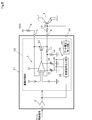
- FIG. 1 is a diagram illustrating a configuration of a drive circuit according to the first embodiment.
- FIG. 2 is a diagram showing a detailed configuration of the amplifier unit.
- FIG. 3 is a diagram illustrating a detailed configuration of a current consumption adjusting unit.
- FIG. 4 is an operation timing chart.
- FIG. 5 is a diagram illustrating a configuration of a drive circuit according to the second embodiment.
- FIG. 6 is an operation timing chart.
- FIG. 7 is a diagram illustrating a configuration of a drive circuit according to the third embodiment.
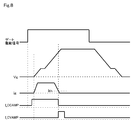
- FIG. 8 is an operation timing chart.
- FIG. 9 is a diagram illustrating a detailed configuration of a current consumption adjusting unit in the fourth embodiment.
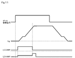
- FIG. 10 is an operation timing chart (No. 1).
- FIG. 11 is an operation timing chart (No. 2).
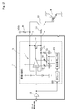
- FIG. 12 is a diagram illustrating a configuration of a drive circuit according to the fifth embodiment.
- FIG. 13 is a diagram illustrating a configuration of a drive circuit according to the sixth embodiment.
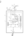
- the drive circuit 1 As shown in FIG. 1, the drive circuit 1 according to the present embodiment includes a buffer 2 and a drive control unit 3. A gate drive signal input from the outside is given to the drive control unit 3 via the buffer 2.
- the drive control unit 3 drives a gate of a switching element, for example, an IGBT (Insulated Gate Bipolar Transistor) 4.
- the IGBT 4 has a current detecting emitter for detecting a collector current.
- the IGBT 4 is, for example, an element that forms an inverter circuit.
- the drive control unit 3 includes an amplifier unit 5 and a current control unit 6.
- the amplifier unit 5 drives the gate of the IGBT 4 with a constant current and a constant voltage.
- the input terminal 7 of the drive circuit 1 is connected to a power supply VDD via an external resistor 8.
- the output terminal 9 of the drive circuit 1 is connected to the gate of the IGBT 4 via an external resistor 10.
- the drive circuit 1 is configured as an integrated circuit.
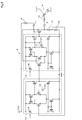
- the amplifier section 5 is configured by a combination of a constant current control amplifier 11 and a constant voltage control amplifier 12. A description of a detailed configuration known as an amplifier will be omitted.
- the input terminal 7 is connected to an inverting input terminal of the constant current control amplifier 11.
- a P-channel MOSFET 13 is connected between the input terminal 7 and the output terminal 9.
- Another inverting input terminal of the constant current control amplifier 11 is connected to an output terminal of the constant voltage control amplifier 12.
- the non-inverting input terminal of the constant current control amplifier 11 is connected to the negative electrode of the voltage source 14.
- the positive electrode of the voltage source 14 is connected to the power supply VDD.
- the output terminal of the constant current control amplifier 11 is connected to the gate of the FET 13.
- the non-inverting input terminal of the constant voltage control amplifier 12 is connected to the positive terminal of the voltage source 15.
- the inverting input terminal of the constant voltage control amplifier 12 is connected to ground via a resistor 16 and to the output terminal 9 via a resistor 17.
- the constant current control amplifier 11 corresponds to a constant current driver
- the constant voltage control amplifier 12 corresponds to a constant voltage driver.
- the voltages of the voltage sources 14 and 15 are Vref1 and Vref2, respectively, the resistance value of the resistance element 8 is Rshunt, and the current flowing through the resistance element 8 is Ig.
- the constant voltage control amplifier 12 controls the constant current control amplifier 11 so that the gate voltage divided by the resistance elements 17 and 16 becomes equal to the voltage Vref2.
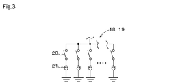
- the constant current control amplifier 11 and the constant voltage control amplifier 12 include current consumption adjusting units 18 and 19, respectively. These are configured by connecting a plurality of series circuits of a switch 20 and a current source 21 in parallel, for example, as shown in FIG.
- the on / off control of the switch 20 is performed by the current control unit 6.
- the current control unit 6 includes a counter 22 and a control signal output unit 23, and a gate drive signal is input to the counter 22 via the buffer 2.
- the counter 22 performs a counting operation during a period in which the gate drive signal indicates a high level.
- the control signal output unit 23 controls the current consumption adjusting units 18 and 19 according to the count value.
- the counter 22 corresponds to a time monitoring unit.
- the control signal output unit 23 controls the current consumption adjusting units 18 and 19 so as to reduce the current consumption of the constant current control amplifier 11 and the constant voltage control amplifier 12.
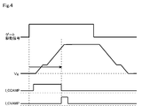
- the amplifier unit 5 starts operating, and the counter 22 starts counting.
- the control signal output unit 23 controls the current consumption adjusting unit 18 and I_CCAMP in FIG. 4 so as to increase the current consumption of the constant current control amplifier 11. Accordingly, the constant current control amplifier 11 starts operating, and flows a constant current Ig to the gate of the IGBT 4. Then, the gate capacitance of the IGBT 4 is charged, and the gate voltage starts to increase.
- the control signal output unit 23 controls the current consumption adjusting unit 18 to reduce the current consumption of the constant current control amplifier 11. I do. At the same time, the control signal output unit 23 controls the current consumption adjusting unit 19 and I_CVAMP in FIG. 4 so as to increase the current consumption of the constant voltage control amplifier 12. Accordingly, the constant voltage control amplifier 12 starts operating, and the gate voltage is controlled to be a voltage corresponding to the voltage Vref2.
- the control signal output unit 23 reduces the current consumption of the constant voltage control amplifier 12.
- the current consumption adjusting unit 19 is controlled so as to perform the operation.
- the counter 22 is cleared to zero. Note that a period until the count value of the counter 22 reaches the first predetermined value corresponds to a first period, and a period from when the counter value reaches the first predetermined value to when it reaches the second predetermined value corresponds to a second period.
- the drive circuit 1 includes the constant current control amplifier 11 and the constant voltage control amplifier 12, and the current consumption adjusting units 18 and 19 for controlling the current consumption of the amplifiers. Then, the current control unit 6 individually controls the current consumption adjusting units 18 and 19 based on the driving state of the gate of the IGBT 4. According to this configuration, in the process of driving the gate of the IGBT 4, the current consumption of each of the constant current control amplifier 11 and the constant voltage control amplifier 12 is optimally adjusted and reduced in accordance with the operating condition. Can be.
- the current consumption of the constant current control amplifier 11 and the constant voltage control amplifier 12 is reduced. Only the control amplifier 12 reduces the current consumption. Then, in the second period following the first period, the current consumption is reduced only to the constant current control amplifier 11, and when the second period ends, the current consumption of the constant current control amplifier 11 and the constant voltage control amplifier 12 is reduced again.
- the constant current drive by the constant current control amplifier 11 is performed, so that the current consumption of the constant voltage control amplifier 12 is reduced.
- the constant voltage drive by the constant voltage control amplifier 12 is performed, so that the current consumption of the constant current control amplifier 11 is reduced.
- the current control unit 6 terminates the first period and ends the second period when a certain period of time has elapsed since the count value of the counter 22 has reached the first predetermined value from the point in time when the gate drive signal has turned on. To start. Then, when the count value of the counter 22 reaches the second predetermined value, the second period ends. Thereby, the lengths of the first period and the second period can be adjusted according to the count value of the counter 22.
- the current consumption adjustments 18 and 19 are configured by a series circuit of the switch 20 and the current source 21 and a plurality of the series circuits are connected in parallel, the current consumption can be adjusted with a simple configuration.
- the drive circuit 31 includes a drive control unit 32 instead of the drive control unit 3.
- the drive control unit 32 includes a current control unit 33 replacing the current control unit 6.
- the current control unit 33 includes a gate voltage monitoring unit 34 and a control signal output unit 35.
- the gate voltage of the IGBT 4 is input to the gate voltage monitor 34 via the input terminal 36 of the drive circuit 31.
- the gate voltage monitor 34 corresponds to a voltage monitor.
- the gate voltage monitoring unit When the gate voltage reaches the threshold value Vth, the gate voltage monitoring unit outputs a trigger signal to the control signal output unit.
- the gate drive signal is input to the control signal output unit 35 via the buffer 2.
- the control signal output unit 35 reduces the current consumption of the constant current control amplifier 11 and the constant voltage control amplifier 12 during the period when the gate drive signal is at the low level, as in the first embodiment. It controls the current consumption adjusters 18 and 19.
- the control signal output unit 35 outputs the current consumption of the constant current control amplifier 11 before the amplifier unit 5 starts increasing the gate voltage of the IGBT 4. Is controlled to increase the current consumption. Then, constant current driving by the constant current control amplifier 11 is performed.
- the gate voltage monitoring unit 34 When the gate voltage reaches the threshold voltage Vth after exceeding the mirror voltage, the gate voltage monitoring unit 34 outputs a trigger signal to the control signal output unit 35. This ends the first period and starts the second period. Then, the control signal output unit 35 controls the current consumption adjusting unit 18 so as to reduce the current consumption of the constant current control amplifier 11, and the constant current driving ends. Further, the control signal output unit 35 controls the current consumption adjusting unit 19 so as to increase the current consumption of the constant voltage control amplifier 12, and accordingly, the constant voltage control amplifier 12 starts operating to perform the constant voltage drive. Is
- control signal output unit 35 controls the current consumption adjusting unit 19 so as to reduce the current consumption of the constant voltage control amplifier 12 when a certain period of time elapses after the IGBT 4 is fully turned on after the trigger signal is supplied. Control. Accordingly, the constant voltage driving ends.
- the current control unit 33 includes the gate voltage monitoring unit 34 that monitors the gate voltage of the IGBT 4, and starts the second period when the gate voltage reaches the threshold Vth.
- the current consumption of the constant current control amplifier 11 and the constant voltage control amplifier 12 can be optimally reduced according to the change in the gate voltage of the IGBT 4.
- the drive circuit 41 includes a drive control unit 42.
- the drive control unit 42 includes a current control unit 43.
- the current control unit 43 is obtained by replacing the gate voltage monitoring unit 34 of the second embodiment with a current monitoring unit 44.
- the current monitor 44 monitors a current flowing between the input terminal 9 and the gate of the IGBT 4. Then, the current monitoring unit 44 outputs a trigger signal to the control signal output unit 35 when the current value being monitored falls below the threshold value It in the process of decreasing.
- the current monitor 44 corresponds to a current monitor.
- the control signal output unit 35 when the gate drive signal changes from a low level to a high level, the control signal output unit 35 operates in the same manner as in the second embodiment. Then, when the gate current Ig decreases and falls below the threshold value It just before the IGBT 4 approaches the full-on state, the current monitor unit 44 outputs a trigger signal to the control signal output unit 35. This ends the first period and starts the second period. Then, the control signal output unit 35 controls the current consumption adjusting unit 18 so as to reduce the current consumption of the constant current control amplifier 11, and the constant current driving ends.
- control signal output unit 35 controls the current consumption adjusting unit 19 so as to increase the current consumption of the constant voltage control amplifier 12, and accordingly, the constant voltage control amplifier 12 starts operating to perform the constant voltage drive. Is Subsequent operations are the same as in the second embodiment.
- the current control unit 43 includes the current monitoring unit 44 that monitors the gate current of the IGBT 4, and starts the second period when the gate current falls below the threshold Ith. Therefore, the current consumption of the constant current control amplifier 11 and the constant voltage control amplifier 12 can be optimally reduced according to the change in the gate current.
- the current flowing between the power supply VDD and the source of the FET 13 may be monitored.
- a shunt resistor may be connected to the current detecting emitter of the IGBT 4, and the current monitor 44 may monitor the current by the terminal voltage of the shunt resistor 45.
- a current sensor may be used.
- the fourth embodiment includes current consumption adjusting units 45 and 46 instead of the current consumption adjusting units 18 and 19.
- a series circuit of a P-channel MOSFET 47 and a resistance element 48 is connected between the constant current control amplifier 11 and the constant voltage control amplifier 12 and the ground, and the drain of the FET 47 is I have.
- the voltage of the variable voltage source 50 is supplied to a non-inverting input terminal of the operational amplifier 49.
- the current consumption adjusting units 45 and 46 are configured as current control amplifiers.
- the current control unit 6 controls the voltage of the variable voltage source 50.
- the current consumption is linearly reduced by the current consumption adjusting unit 45 and the current consumption is linearly increased by the current consumption adjusting unit 46.
- the influence on the gate voltage can be reduced by giving a constant slope to the decrease and increase in the current consumption.
- the drive circuit 1D of the sixth embodiment has a configuration corresponding to the drive control unit 3 of the first embodiment, such that the drive control unit 3D drives the two IGBTs 4A and 4B in parallel. Has a pair.
- the IGBTs 4A and 4B may be turned on and off simultaneously or only one of them may be driven according to the amount of current consumed by the load to be driven.
- the current control unit 6D is adjusted so that the current consumption of the current consumption control units 18 and 19 corresponding to the IGBT 4 not to be driven is maintained in a reduced state.
- the IGBT 4 may not have an emitter for current detection.
- the current consumption adjusting unit may be configured with only one set of the series circuit of the switch 20 and the current source 21.
- the switching element is not limited to the IGBT 4 and may be a voltage-driven element. In the configuration of the sixth embodiment, three or more elements may be driven in parallel. The respective embodiments may be implemented in combination as appropriate.
Landscapes
- Engineering & Computer Science (AREA)
- Power Engineering (AREA)
- Power Conversion In General (AREA)
- Electronic Switches (AREA)
Abstract
本開示の一態様は、駆動回路1に、定電流制御アンプ11及び定電圧制御アンプ12,並びにそれらの消費電流をそれぞれ制御する消費電流調整部18及び19を備える。そして、電流制御部6は、IGBT4のゲートの駆動状態に基づき、消費電流調整部18及び19を個別に制御する。
Description
本出願は、2018年6月27日に出願された日本出願番号2018-121898号に基づくもので、ここにその記載内容を援用する。
本開示は、電圧駆動型のスイッチング素子を駆動する回路に関する。
例えばIGBT等のパワー系のスイッチング素子を駆動する回路として、例えば特許文献1には、以下のような構成が開示されている。定電流生成部30から流れ込む定電流の大きさに応じたオン時間でスイッチング素子50をオンするドライバ回路40を備える。定電流生成部30は、スイッチング素子50がオンするオン時間に達するまで大きい定電流を流してスイッチング素子50の立上がり速度を高速に維持する。オン時間が経過した後は、小さい定電流を流してドライバ回路40の消費電流を低減する。
ここで、駆動回路に定電流アンプ及び定電圧アンプを備え、スイッチング素子を定電流定電圧駆動することを想定する。このように構成される駆動回路では、IGBTのゲートに印加する電圧を立ち上げる初期の段階では、定電流アンプによりゲート電圧の立上り速度を制御し、立上りの後半では定電圧アンプによってゲート電圧を所定の電圧に制御することが考えられる。また、この構成では、2つのアンプを使用することで消費電流が多くなるという問題がある。
本開示は上記事情に鑑みてなされたものであり、その目的は、電圧駆動型のスイッチング素子を定電流定電圧駆動する際に、消費電流を最適に低減できるスイッチング素子の駆動回路を提供することにある。
本開示のスイッチング素子の駆動回路によれば、スイッチング素子のゲートを定電流駆動する定電流駆動部,及び同ゲートを定電圧駆動する定電圧駆動部に、内部における消費電流を調整する消費電流調整部を備える。そして、電流制御部は、前記ゲートの駆動状態に基づき、定電流駆動部及び定電圧駆動部の消費電流調整部を個別に制御する。このように構成すれば、スイッチング素子のゲートを駆動する過程で、定電流駆動部,定電圧駆動部のそれぞれが動作する状況に応じて、それぞれの消費電流を最適に調整して低減することができる。
また、本開示のスイッチング素子の駆動回路によれば、電流制御部は、駆動信号がオフレベルであれば定電流駆動部及び定電圧駆動部の消費電流を低減させ、駆動信号がオンレベルになった時点から第1期間までは定電圧駆動部のみに消費電流を低減させる。そして、第1期間に続く第2期間では定電流駆動部のみに消費電流を低減させ、第2期間が終了すると定電流駆動部及び定電圧駆動部の消費電流を低減させる。
すなわち、スイッチング素子のターンオンを開始させた直後からの第1期間は、定電流駆動部による定電流駆動を行うため、定電圧駆動部の消費電流を低減させる。そして、第1期間に続く第2期間では、定電圧駆動部による定電圧駆動を行うので、定電流駆動部の消費電流を低減させる。このように構成すれば、スイッチング素子のターンオンを制御する形態に応じて消費電流を効率的に低減できる。
本開示についての上記目的およびその他の目的、特徴や利点は、添付の図面を参照しながら下記の詳細な記述により、より明確になる。その図面は、
図1は、第1実施形態において、駆動回路の構成を示す図であり、
図2は、アンプ部の詳細構成を示す図であり、
図3は、消費電流調整部の詳細構成を示す図であり、
図4は、動作タイミングチャートであり、
図5は、第2実施形態において、駆動回路の構成を示す図であり、
図6は、動作タイミングチャートであり、
図7は、第3実施形態において、駆動回路の構成を示す図であり、
図8は、動作タイミングチャートであり、
図9は、第4実施形態において、消費電流調整部の詳細構成を示す図であり、
図10は、動作タイミングチャート(その1)であり、
図11は、動作タイミングチャート(その2)であり、
図12は、第5実施形態において、駆動回路の構成を示す図であり、
図13は、第6実施形態において、駆動回路の構成を示す図である。
(第1実施形態)
図1に示すように、本実施形態の駆動回路1は、バッファ2及び駆動制御部3を備えている。外部より入力されるゲート駆動信号は、バッファ2を介して駆動制御部3に与えられる。駆動制御部3は、スイッチング素子である例えばIGBT(Insulated Gate Bipolar Transistor)4のゲートを駆動する。IGBT4は、コレクタ電流を検出するための電流検出用エミッタを有している。IGBT4は、例えばインバータ回路を構成する素子である。
図1に示すように、本実施形態の駆動回路1は、バッファ2及び駆動制御部3を備えている。外部より入力されるゲート駆動信号は、バッファ2を介して駆動制御部3に与えられる。駆動制御部3は、スイッチング素子である例えばIGBT(Insulated Gate Bipolar Transistor)4のゲートを駆動する。IGBT4は、コレクタ電流を検出するための電流検出用エミッタを有している。IGBT4は、例えばインバータ回路を構成する素子である。
駆動制御部3は、アンプ部5及び電流制御部6を備えている。アンプ部5は、IGBT4のゲートを定電流・定電圧駆動する。駆動回路1の入力端子7は、外付けの抵抗素子8を介して電源VDDに接続されている。駆動回路1の出力端子9は、外付けの抵抗素子10を介してIGBT4のゲートに接続されている。尚、駆動回路1は、集積回路として構成されている。
図2に示すように、アンプ部5は、定電流制御アンプ11及び定電圧制御アンプ12の組み合わせで構成されている。尚、アンプとして周知の詳細構成に関する説明は省略する。入力端子7は、定電流制御アンプ11の反転入力端子に接続されている。入力端子7と出力端子9との間には、PチャネルMOSFET13が接続されている。定電流制御アンプ11のもう1つの反転入力端子は、定電圧制御アンプ12の出力端子に接続されている。定電流制御アンプ11の非反転入力端子は、電圧源14の負極に接続されている。電圧源14の正極は、電源VDDに接続されている。定電流制御アンプ11の出力端子は、FET13のゲートに接続されている。
定電圧制御アンプ12の非反転入力端子は、電圧源15の正極に接続されている。定電圧制御アンプ12の反転入力端子は、抵抗素子16を介してグランドに接続されていると共に、抵抗素子17を介して出力端子9に接続されている。定電流制御アンプ11は定電流駆動部に相当し、定電圧制御アンプ12は定電圧駆動部に相当する。
ここで、電圧源14,15の電圧をそれぞれVref1,Vref2とし、抵抗素子8の抵抗値をRshunt,抵抗素子8に流れる電流をIgとする。この場合、定電流制御アンプ11の反転入力端子の電位は(VDD-Vref1)となるから、電流Igは
Ig=Vref1/Rshunt
となる。したがって、例えばVref1=1V,Rshunt=1Ωに設定すればIg=1Aとなり、FET13を介してIGBT4のゲートに1Aの電流を流すことができる。
また、定電圧制御アンプ12は、抵抗素子17及び16で分圧されたゲート電圧が、電圧Vref2に等しくなるように定電流制御アンプ11を制御する。
Ig=Vref1/Rshunt
となる。したがって、例えばVref1=1V,Rshunt=1Ωに設定すればIg=1Aとなり、FET13を介してIGBT4のゲートに1Aの電流を流すことができる。
また、定電圧制御アンプ12は、抵抗素子17及び16で分圧されたゲート電圧が、電圧Vref2に等しくなるように定電流制御アンプ11を制御する。
図1に示すように、定電流制御アンプ11及び定電圧制御アンプ12は、それぞれ消費電流調整部18及び19を備えている。これらは、例えば図3に示すように、スイッチ20及び電流源21の直列回路を複数並列に接続して構成されている。スイッチ20のオンオフ制御は、電流制御部6により行われる。電流制御部6は、カウンタ22及び制御信号出力部23を備え、カウンタ22には、バッファ2を介してゲート駆動信号が入力されている。カウンタ22は、ゲート駆動信号がハイレベルを示す期間にカウント動作を行う。制御信号出力部23は、そのカウント値に応じて消費電流調整部18及び19を制御する。カウンタ22は時間監視部に相当する。
次に、本実施形態の作用について説明する。図4に示すように、ゲート駆動信号がオフレベルのローを示している期間は、カウンタ22はゼロクリアされている。この期間はアンプ部5が動作しないので、制御信号出力部23は、定電流制御アンプ11及び定電圧制御アンプ12の消費電流を低減するように、消費電流調整部18及び19を制御する。そして、ゲート駆動信号がオンレベルのハイに変化するとアンプ部5が動作を開始し、カウンタ22がカウント動作を開始する。
制御信号出力部23は、カウンタ22のカウント値が変化し始めると、定電流制御アンプ11の消費電流を増加させるように消費電流調整部18,図4中のI_CCAMPを制御する。これに伴い定電流制御アンプ11が動作を開始して、IGBT4のゲートに一定の電流Igを流す。すると、IGBT4のゲート容量が充電されて、ゲート電圧は上昇を開始する。
ゲート電圧がミラー電圧を超えた後にカウンタ22のカウント値が第1所定値に達すると、制御信号出力部23は、定電流制御アンプ11の消費電流を低減させるように消費電流調整部18を制御する。同時に、制御信号出力部23は、定電圧制御アンプ12の消費電流を増加させるように消費電流調整部19,図4中のI_CVAMPを制御する。これに伴い定電圧制御アンプ12が動作を開始して、ゲート電圧は電圧Vref2に応じた電圧となるように制御される。
そして、ゲート電圧が前記電圧に達してIGBT4がフルオン状態になった後、カウンタ22のカウント値が第2所定値に達すると、制御信号出力部23は、定電圧制御アンプ12の消費電流を低減するように消費電流調整部19を制御する。この時点で、カウンタ22はゼロクリアされる。尚、カウンタ22のカウント値が第1所定値に達するまでの期間は第1期間に相当し、第1所定値に達してから第2所定値に達するまでの期間が第2期間に相当する。
以上のように本実施形態によれば、駆動回路1に、定電流制御アンプ11及び定電圧制御アンプ12,並びにそれらの消費電流をそれぞれ制御する消費電流調整部18及び19を備える。そして、電流制御部6は、IGBT4のゲートの駆動状態に基づき、消費電流調整部18及び19を個別に制御する。このように構成すれば、IGBT4のゲートを駆動する過程で、定電流制御アンプ11,定電圧制御アンプ12のそれぞれが動作する状況に応じて、それぞれの消費電流を最適に調整して低減することができる。
具体的には、ゲート駆動信号がオフレベルであれば定電流制御アンプ11及び定電圧制御アンプ12の消費電流を低減させ、ゲート駆動信号がオンレベルになった時点から第1期間までは定電圧制御アンプ12のみに消費電流を低減させる。そして、第1期間に続く第2期間では定電流制御アンプ11のみに消費電流を低減させ、第2期間が終了すると再び定電流制御アンプ11及び定電圧制御アンプ12の消費電流を低減させる。
すなわち、IGBT4のターンオンを開始させた直後からの第1期間は、定電流制御アンプ11による定電流駆動を行うため、定電圧制御アンプ12の消費電流を低減させる。そして、第1期間に続く第2期間では定電圧制御アンプ12による定電圧駆動を行うので、定電流制御アンプ11の消費電流を低減させる。このように構成すれば、IGBT4のターンオンを制御する形態に応じて消費電流を効率的に低減できる。
そして、電流制御部6は、ゲート駆動信号がオンレベルになった時点から、カウンタ22のカウント値が第1所定値に達することで一定時間が経過すると、第1期間を終了して第2期間を開始する。そして、カウンタ22のカウント値が第2所定値に達すると第2期間を終了する。これにより、カウンタ22のカウント値に応じて、第1期間及び第2期間の長さを調整できる。また、消費電流調整18及び19を、スイッチ20と電流源21との直列回路で構成し、その直列回路を複数並列に接続して構成したので、簡単な構成で消費電流を調整できる。
(第2実施形態)
以下、第1実施形態と同一部分には同一符号を付して説明を省略し、異なる部分について説明する。図5に示すように、第2実施形態の駆動回路31は、駆動制御部3に替わる駆動制御部32を備えている。駆動制御部32は、電流制御部6に替わる電流制御部33を備えている。電流制御部33は、ゲート電圧モニタ部34及び制御信号出力部35を備えている。
以下、第1実施形態と同一部分には同一符号を付して説明を省略し、異なる部分について説明する。図5に示すように、第2実施形態の駆動回路31は、駆動制御部3に替わる駆動制御部32を備えている。駆動制御部32は、電流制御部6に替わる電流制御部33を備えている。電流制御部33は、ゲート電圧モニタ部34及び制御信号出力部35を備えている。
ゲート電圧モニタ部34には、駆動回路31の入力端子36を介してIGBT4のゲート電圧が入力されている。ゲート電圧モニタ部34は電圧監視部に相当する。ゲート電圧モニタ部34は、ゲート電圧が閾値Vthに達すると、制御信号出力部35にトリガ信号を出力する。制御信号出力部35には、バッファ2を介してゲート駆動信号が入力されている。
次に、第2実施形態の作用について説明する。図6に示すように、制御信号出力部35は、ゲート駆動信号がローレベルの期間は第1実施形態と同様に、定電流制御アンプ11及び定電圧制御アンプ12の消費電流を低減するように消費電流調整部18及び19を制御する。ゲート駆動信号がハイレベルに変化するとアンプ部5が動作を開始するが、制御信号出力部35は、アンプ部5がIGBT4のゲート電圧の上昇を開始させる前に、定電流制御アンプ11の消費電流を増加させるように消費電流調整部18を制御する。そして、定電流制御アンプ11による定電流駆動が行われる。
ゲート電圧がミラー電圧を超えた後閾値電圧Vthに達すると、ゲート電圧モニタ部34が制御信号出力部35にトリガ信号を出力する。これにより第1期間が終了し、第2期間の開始となる。すると、制御信号出力部35は、定電流制御アンプ11の消費電流を低減させるように消費電流調整部18を制御し、定電流駆動が終了する。また、制御信号出力部35は、定電圧制御アンプ12の消費電流を増加させるように消費電流調整部19を制御し、これに伴い定電圧制御アンプ12が動作を開始して定電圧駆動が行われる。
そして、制御信号出力部35は、トリガ信号が与えられてからIGBT4がフルオン状態になった後、一定時間が経過すると、定電圧制御アンプ12の消費電流を低減するように消費電流調整部19を制御する。これに伴い、定電圧駆動が終了する。
以上のように第2実施形態によれば、電流制御部33は、IGBT4のゲート電圧を監視するゲート電圧モニタ部34を備え、ゲート電圧が閾値Vthに達すると第2期間を開始する。これにより、IGBT4のゲート電圧の変化に応じて、定電流制御アンプ11及び定電圧制御アンプ12の消費電流を最適に低減することができる。
(第3実施形態)
図7に示すように、第3実施形態の駆動回路41は、駆動制御部42を備えている。駆動制御部42は、電流制御部43を備えている。電流制御部43は、第2実施形態のゲート電圧モニタ部34を電流モニタ部44に置き換えたものである。電流モニタ部44は、入力端子9とIGBT4のゲートとの間に流れる電流を監視する。そして、電流モニタ部44は、監視している電流値が減少する過程で閾値Itを下回ると、制御信号出力部35にトリガ信号を出力する。電流モニタ部44は電流監視部に相当する。
図7に示すように、第3実施形態の駆動回路41は、駆動制御部42を備えている。駆動制御部42は、電流制御部43を備えている。電流制御部43は、第2実施形態のゲート電圧モニタ部34を電流モニタ部44に置き換えたものである。電流モニタ部44は、入力端子9とIGBT4のゲートとの間に流れる電流を監視する。そして、電流モニタ部44は、監視している電流値が減少する過程で閾値Itを下回ると、制御信号出力部35にトリガ信号を出力する。電流モニタ部44は電流監視部に相当する。
次に、第3実施形態の作用について説明する。図8に示すように、制御信号出力部35は、ゲート駆動信号がローレベルからハイレベルに変化すると、第2実施形態と同様に動作する。そして、IGBT4がフルオン状態に近付く直前にゲート電流Igが減少して閾値Itを下回ると、電流モニタ部44は制御信号出力部35にトリガ信号を出力する。これにより第1期間が終了し、第2期間の開始となる。すると、制御信号出力部35は、定電流制御アンプ11の消費電流を低減させるように消費電流調整部18を制御し、定電流駆動が終了する。また、制御信号出力部35は、定電圧制御アンプ12の消費電流を増加させるように消費電流調整部19を制御し、これに伴い定電圧制御アンプ12が動作を開始して定電圧駆動が行われる。以降の動作は第2実施形態と同様である。
以上ように第3実施形態によれば、電流制御部43は、IGBT4のゲート電流を監視する電流モニタ部44を備え、ゲート電流が閾値Ithを下回ると第2期間を開始する。これにより、ゲート電流の変化に応じて、定電流制御アンプ11及び定電圧制御アンプ12の消費電流を最適に低減することができる。
その他、電源VDDとFET13のソースとの間に流れる電流を監視しても良い。また、IGBT4の電流検出用エミッタにシャント抵抗を接続し、電流モニタ部44はシャント抵抗45の端子電圧により電流を監視しても良い。また、電流センサを用いても良い。
(第4実施形態)
第4実施形態は、図9に示すように、消費電流調整部18及び19に替えて、消費電流調整部45及び46を備える。定電流制御アンプ11及び定電圧制御アンプ12とグランドとの間には、PチャネルMOSFET47及び抵抗素子48の直列回路が接続されており、FET47のドレインは、オペアンプ49の反転入力端子に接続されている。オペアンプ49の非反転入力端子には、可変電圧源50の電圧が与えられている。消費電流調整部45及び46は、電流制御アンプとして構成されている。
第4実施形態は、図9に示すように、消費電流調整部18及び19に替えて、消費電流調整部45及び46を備える。定電流制御アンプ11及び定電圧制御アンプ12とグランドとの間には、PチャネルMOSFET47及び抵抗素子48の直列回路が接続されており、FET47のドレインは、オペアンプ49の反転入力端子に接続されている。オペアンプ49の非反転入力端子には、可変電圧源50の電圧が与えられている。消費電流調整部45及び46は、電流制御アンプとして構成されている。
次に、第4実施形態の作用について説明する。例えば第1実施形態の構成において、電流制御部6に可変電圧源50の電圧を制御させる。これにより、第1期間から第2期間に移行させる際に、消費電流調整部45により消費電流をリニアに減少させ、消費電流調整部46により消費電流をリニアに増加させる。
すなわち、第1実施形態のようにスイッチ20のオンオフで制御すると消費電流の変化量が大きくなり、第1期間から第2期間に移行する過程でゲート電圧にリンギングが発生する可能性が有る。これに対して、図10に示すように、消費電流の減少及び増加に一定の傾きを付与することで、ゲート電圧に与える影響を低減できる。
また、第4実施形態の構成によれば、図11に示すように、第1期間において消費電流調整部46により消費電流を低減するレベルを、第1実施形態よりも若干上昇させる制御も可能になる。これにより、消費電流は若干増加するが、第1期間から第2期間に移行する際の電流変化量が小さくなるので、図10のケースと同様の効果が得られる。尚、図10に示す制御と併せて行っても良い。
(第5実施形態)
図12に示すように、第5実施形態では、第1実施形態の駆動回路1によりIGBT4を駆動する際に、外付けのNPNトランジスタ51を追加してIGBT4とダーリントン接続する。トランジスタ51のコレクタは入力端子7に接続され、ベースは抵抗素子10に接続されている。そして、トランジスタ51のエミッタはIGBT4のゲートに接続されている。すなわち、駆動回路1がトランジスタ51を介してIGBT4を駆動する。これにより、IGBT4のゲートには、トランジスタ51を介して駆動電流が供給されるので、アンプ部5の消費電流を低減できる。
図12に示すように、第5実施形態では、第1実施形態の駆動回路1によりIGBT4を駆動する際に、外付けのNPNトランジスタ51を追加してIGBT4とダーリントン接続する。トランジスタ51のコレクタは入力端子7に接続され、ベースは抵抗素子10に接続されている。そして、トランジスタ51のエミッタはIGBT4のゲートに接続されている。すなわち、駆動回路1がトランジスタ51を介してIGBT4を駆動する。これにより、IGBT4のゲートには、トランジスタ51を介して駆動電流が供給されるので、アンプ部5の消費電流を低減できる。
(第6実施形態)
図13に示すように、第6実施形態の駆動回路1Dは、駆動制御部3Dが2つのIGBT4A,4Bを並列に駆動するように、第1実施形態の駆動制御部3に対応する構成を2組備えている。この場合、駆動される負荷の消費電流量に応じてIGBT4A及び4Bを同時にオンオフさせても良いし、何れか一方のみを駆動させても良い。後者のケースについては、駆動させない方のIGBT4に対応する消費電流制御部18及び19の消費電流を低減した状態に維持するように、電流制御部6Dを調整する。
図13に示すように、第6実施形態の駆動回路1Dは、駆動制御部3Dが2つのIGBT4A,4Bを並列に駆動するように、第1実施形態の駆動制御部3に対応する構成を2組備えている。この場合、駆動される負荷の消費電流量に応じてIGBT4A及び4Bを同時にオンオフさせても良いし、何れか一方のみを駆動させても良い。後者のケースについては、駆動させない方のIGBT4に対応する消費電流制御部18及び19の消費電流を低減した状態に維持するように、電流制御部6Dを調整する。
(その他の実施形態)
IGBT4は、電流検出用のエミッタを有しないものでも良い。
スイッチ20及び電流源21の直列回路を1組だけで消費電流調整部を構成しても良い。
スイッチング素子はIGBT4に限ることなく、電圧駆動型の素子であれば良い。
第6実施形態の構成において、3素子以上を並列に駆動するように構成しても良い。
各実施形態を適宜組み合わせて実施しても良い。
IGBT4は、電流検出用のエミッタを有しないものでも良い。
スイッチ20及び電流源21の直列回路を1組だけで消費電流調整部を構成しても良い。
スイッチング素子はIGBT4に限ることなく、電圧駆動型の素子であれば良い。
第6実施形態の構成において、3素子以上を並列に駆動するように構成しても良い。
各実施形態を適宜組み合わせて実施しても良い。
本開示は、実施例に準拠して記述されたが、本開示は当該実施例や構造に限定されるものではないと理解される。本開示は、様々な変形例や均等範囲内の変形をも包含する。加えて、様々な組み合わせや形態、さらには、それらに一要素のみ、それ以上、あるいはそれ以下、を含む他の組み合わせや形態をも、本開示の範疇や思想範囲に入るものである。
Claims (11)
- 入力される駆動信号に応じて電圧駆動型のスイッチング素子(4)を駆動するもので、
前記スイッチング素子のゲートを定電流駆動するもので、内部における消費電流を調整する消費電流調整部(18,45)を有する定電流駆動部(11)と、
前記ゲートを定電圧駆動するもので、内部における消費電流を調整する消費電流調整部(19,46)を有する定電圧駆動部(12)と、
前記ゲートの駆動状態に基づいて、前記定電流駆動部及び前記定電圧駆動部の消費電流調整部を個別に制御する電流制御部(6,6D,33,43)とを備えるスイッチング素子の駆動回路。 - 前記電流制御部は、
前記駆動信号がオフレベルであれば、前記定電流駆動部及び前記定電圧駆動部に消費電流を低減させ、
前記駆動信号がオンレベルになった時点から第1期間までは、前記定電圧駆動部のみに消費電流を低減させ、
前記第1期間に続く第2期間では、前記定電流駆動部のみに消費電流を低減させ、
前記第2期間が終了すると、前記定電流駆動部及び前記定電圧駆動部に消費電流を低減させる請求項1記載のスイッチング素子の駆動回路。 - 前記電流制御部(33)は、前記ゲート電圧を監視する電圧監視部(34)を備え、
前記ゲート電圧が閾値に達すると、前記第2期間を開始する請求項2記載のスイッチング素子の駆動回路。 - 前記電流制御部(43)は、前記定電流駆動部より供給される電流を監視する電流監視部(44)を備え、
前記電流が閾値を下回ると、前記第2期間を開始する請求項2又は3記載のスイッチング素子の駆動回路。 - 前記電流制御部(6)は、前記駆動信号がオンレベルになった時点から計時を行う時間監視部(22)を備え、
前記計時時間が一定時間になると、前記第2期間を開始する請求項2から4の何れか一項に記載のスイッチング素子の駆動回路。 - 前記消費電流調整部(46)は、前記第1期間において、前記定電流駆動部の消費電流を一定量流すように制御する請求項2から5の何れか一項に記載のスイッチング素子の駆動回路。
- 前記消費電流調整部(18,19)は、電流源(21)とスイッチ(20)との直列回路で構成される請求項1から6の何れか一項に記載のスイッチング素子の駆動回路。
- 前記消費電流調整部は、前記直列回路を複数備え、それらが並列に接続されて構成される請求項7記載のスイッチング素子の駆動回路。
- 前記消費電流調整部(45,46)は、電流制御アンプで構成される請求項1から6の何れか一項に記載のスイッチング素子の駆動回路。
- 本体が集積回路で構成され、前記集積回路の外部に、前記スイッチング素子に通電する電流量を増幅する電流増幅用素子(51)を備える請求項1から9の何れか一項に記載のスイッチング素子の駆動回路。
- 複数のスイッチング素子を並列に駆動可能に構成される請求項1から10の何れか一項に記載のスイッチング素子の駆動回路。
Applications Claiming Priority (2)
| Application Number | Priority Date | Filing Date | Title |
|---|---|---|---|
| JP2018-121898 | 2018-06-27 | ||
| JP2018121898A JP6848936B2 (ja) | 2018-06-27 | 2018-06-27 | スイッチング素子の駆動回路 |
Publications (1)
| Publication Number | Publication Date |
|---|---|
| WO2020003699A1 true WO2020003699A1 (ja) | 2020-01-02 |
Family
ID=68987022
Family Applications (1)
| Application Number | Title | Priority Date | Filing Date |
|---|---|---|---|
| PCT/JP2019/016316 WO2020003699A1 (ja) | 2018-06-27 | 2019-04-16 | スイッチング素子の駆動回路 |
Country Status (2)
| Country | Link |
|---|---|
| JP (1) | JP6848936B2 (ja) |
| WO (1) | WO2020003699A1 (ja) |
Families Citing this family (2)
| Publication number | Priority date | Publication date | Assignee | Title |
|---|---|---|---|---|
| JP2022085366A (ja) * | 2020-11-27 | 2022-06-08 | 株式会社デンソー | ゲート駆動装置 |
| JP2023136689A (ja) | 2022-03-17 | 2023-09-29 | 富士電機株式会社 | スイッチング素子の駆動回路及びインテリジェントパワーモジュール |
Citations (5)
| Publication number | Priority date | Publication date | Assignee | Title |
|---|---|---|---|---|
| JP2008022451A (ja) * | 2006-07-14 | 2008-01-31 | Toyota Motor Corp | 電力用スイッチング素子の駆動装置 |
| JP2012114585A (ja) * | 2010-11-22 | 2012-06-14 | Denso Corp | 負荷駆動装置の製造方法 |
| JP2012114587A (ja) * | 2010-11-22 | 2012-06-14 | Denso Corp | 負荷駆動装置 |
| JP2012129971A (ja) * | 2010-11-22 | 2012-07-05 | Denso Corp | 負荷駆動装置 |
| JP2015231180A (ja) * | 2014-06-06 | 2015-12-21 | トヨタ自動車株式会社 | 駆動回路及び半導体装置 |
Family Cites Families (4)
| Publication number | Priority date | Publication date | Assignee | Title |
|---|---|---|---|---|
| JP2004228768A (ja) * | 2003-01-21 | 2004-08-12 | Toshiba Corp | ゲート駆動回路 |
| JP4315125B2 (ja) * | 2005-05-11 | 2009-08-19 | トヨタ自動車株式会社 | 電圧駆動型半導体素子の駆動装置 |
| JP5701176B2 (ja) * | 2011-08-04 | 2015-04-15 | 三菱電機株式会社 | ゲート駆動装置 |
| JP5777537B2 (ja) * | 2012-02-17 | 2015-09-09 | 三菱電機株式会社 | パワーデバイス制御回路およびパワーデバイス回路 |
-
2018
- 2018-06-27 JP JP2018121898A patent/JP6848936B2/ja active Active
-
2019
- 2019-04-16 WO PCT/JP2019/016316 patent/WO2020003699A1/ja active Application Filing
Patent Citations (5)
| Publication number | Priority date | Publication date | Assignee | Title |
|---|---|---|---|---|
| JP2008022451A (ja) * | 2006-07-14 | 2008-01-31 | Toyota Motor Corp | 電力用スイッチング素子の駆動装置 |
| JP2012114585A (ja) * | 2010-11-22 | 2012-06-14 | Denso Corp | 負荷駆動装置の製造方法 |
| JP2012114587A (ja) * | 2010-11-22 | 2012-06-14 | Denso Corp | 負荷駆動装置 |
| JP2012129971A (ja) * | 2010-11-22 | 2012-07-05 | Denso Corp | 負荷駆動装置 |
| JP2015231180A (ja) * | 2014-06-06 | 2015-12-21 | トヨタ自動車株式会社 | 駆動回路及び半導体装置 |
Also Published As
| Publication number | Publication date |
|---|---|
| JP2020005085A (ja) | 2020-01-09 |
| JP6848936B2 (ja) | 2021-03-24 |
Similar Documents
| Publication | Publication Date | Title |
|---|---|---|
| US8766671B2 (en) | Load driving apparatus | |
| US9124264B2 (en) | Load driver | |
| JP5862434B2 (ja) | パワートランジスタの駆動回路 | |
| US8222846B2 (en) | Output circuit | |
| US8310296B2 (en) | Driving transistor control circuit | |
| US9923557B2 (en) | Switching circuit and power conversion circuit | |
| EP3148077B1 (en) | Driver for a p-channel mosfet | |
| WO2020003699A1 (ja) | スイッチング素子の駆動回路 | |
| JP2017079534A (ja) | ゲート制御回路 | |
| WO2015033444A1 (ja) | バッファ回路 | |
| JP6478826B2 (ja) | ハイサイドドライバ回路及び半導体装置 | |
| US10056896B2 (en) | Switching element driving device | |
| JP4881582B2 (ja) | 遅延回路および駆動制御回路 | |
| JP2023063081A (ja) | スイッチング回路、dc/dcコンバータおよびその制御回路 | |
| US9318973B2 (en) | Driving device | |
| JP2018207276A (ja) | ゲート駆動回路 | |
| US20130321029A1 (en) | Input decision circuit | |
| JP2017532945A (ja) | 電圧コンバータのためのアダプティブコントローラ | |
| US10734995B1 (en) | Output circuit | |
| US10924103B2 (en) | Driver circuitry | |
| KR101733778B1 (ko) | 스위칭 신호의 제어 장치 및 방법 | |
| US11996675B2 (en) | Laser drive circuit and sensor apparatus | |
| JP2017163722A (ja) | ゲート駆動回路 | |
| WO2020213513A1 (ja) | ゲート駆動回路 | |
| WO2020235224A1 (ja) | 半導体装置 |
Legal Events
| Date | Code | Title | Description |
|---|---|---|---|
| 121 | Ep: the epo has been informed by wipo that ep was designated in this application |
Ref document number: 19827545 Country of ref document: EP Kind code of ref document: A1 |
|
| NENP | Non-entry into the national phase |
Ref country code: DE |
|
| 122 | Ep: pct application non-entry in european phase |
Ref document number: 19827545 Country of ref document: EP Kind code of ref document: A1 |