WO2020003055A1 - 半導体装置の作製方法 - Google Patents
半導体装置の作製方法 Download PDFInfo
- Publication number
- WO2020003055A1 WO2020003055A1 PCT/IB2019/055127 IB2019055127W WO2020003055A1 WO 2020003055 A1 WO2020003055 A1 WO 2020003055A1 IB 2019055127 W IB2019055127 W IB 2019055127W WO 2020003055 A1 WO2020003055 A1 WO 2020003055A1
- Authority
- WO
- WIPO (PCT)
- Prior art keywords
- layer
- metal oxide
- insulating layer
- film
- transistor
- Prior art date
- Legal status (The legal status is an assumption and is not a legal conclusion. Google has not performed a legal analysis and makes no representation as to the accuracy of the status listed.)
- Ceased
Links
Images








Classifications
-
- H—ELECTRICITY
- H10—SEMICONDUCTOR DEVICES; ELECTRIC SOLID-STATE DEVICES NOT OTHERWISE PROVIDED FOR
- H10D—INORGANIC ELECTRIC SEMICONDUCTOR DEVICES
- H10D99/00—Subject matter not provided for in other groups of this subclass
-
- H—ELECTRICITY
- H10—SEMICONDUCTOR DEVICES; ELECTRIC SOLID-STATE DEVICES NOT OTHERWISE PROVIDED FOR
- H10D—INORGANIC ELECTRIC SEMICONDUCTOR DEVICES
- H10D30/00—Field-effect transistors [FET]
- H10D30/60—Insulated-gate field-effect transistors [IGFET]
- H10D30/67—Thin-film transistors [TFT]
- H10D30/6704—Thin-film transistors [TFT] having supplementary regions or layers in the thin films or in the insulated bulk substrates for controlling properties of the device
- H10D30/6713—Thin-film transistors [TFT] having supplementary regions or layers in the thin films or in the insulated bulk substrates for controlling properties of the device characterised by the properties of the source or drain regions, e.g. compositions or sectional shapes
-
- H—ELECTRICITY
- H10—SEMICONDUCTOR DEVICES; ELECTRIC SOLID-STATE DEVICES NOT OTHERWISE PROVIDED FOR
- H10D—INORGANIC ELECTRIC SEMICONDUCTOR DEVICES
- H10D30/00—Field-effect transistors [FET]
- H10D30/60—Insulated-gate field-effect transistors [IGFET]
- H10D30/67—Thin-film transistors [TFT]
- H10D30/6729—Thin-film transistors [TFT] characterised by the electrodes
- H10D30/6737—Thin-film transistors [TFT] characterised by the electrodes characterised by the electrode materials
- H10D30/6739—Conductor-insulator-semiconductor electrodes
-
- H—ELECTRICITY
- H10—SEMICONDUCTOR DEVICES; ELECTRIC SOLID-STATE DEVICES NOT OTHERWISE PROVIDED FOR
- H10D—INORGANIC ELECTRIC SEMICONDUCTOR DEVICES
- H10D30/00—Field-effect transistors [FET]
- H10D30/60—Insulated-gate field-effect transistors [IGFET]
- H10D30/67—Thin-film transistors [TFT]
- H10D30/674—Thin-film transistors [TFT] characterised by the active materials
- H10D30/6755—Oxide semiconductors, e.g. zinc oxide, copper aluminium oxide or cadmium stannate
-
- H—ELECTRICITY
- H10—SEMICONDUCTOR DEVICES; ELECTRIC SOLID-STATE DEVICES NOT OTHERWISE PROVIDED FOR
- H10D—INORGANIC ELECTRIC SEMICONDUCTOR DEVICES
- H10D86/00—Integrated devices formed in or on insulating or conducting substrates, e.g. formed in silicon-on-insulator [SOI] substrates or on stainless steel or glass substrates
- H10D86/01—Manufacture or treatment
- H10D86/021—Manufacture or treatment of multiple TFTs
-
- H—ELECTRICITY
- H10—SEMICONDUCTOR DEVICES; ELECTRIC SOLID-STATE DEVICES NOT OTHERWISE PROVIDED FOR
- H10K—ORGANIC ELECTRIC SOLID-STATE DEVICES
- H10K59/00—Integrated devices, or assemblies of multiple devices, comprising at least one organic light-emitting element covered by group H10K50/00
- H10K59/10—OLED displays
- H10K59/12—Active-matrix OLED [AMOLED] displays
-
- H—ELECTRICITY
- H10—SEMICONDUCTOR DEVICES; ELECTRIC SOLID-STATE DEVICES NOT OTHERWISE PROVIDED FOR
- H10P—GENERIC PROCESSES OR APPARATUS FOR THE MANUFACTURE OR TREATMENT OF DEVICES COVERED BY CLASS H10
- H10P32/00—Diffusion of dopants within, into or out of wafers, substrates or parts of devices
- H10P32/10—Diffusion of dopants within, into or out of semiconductor bodies or layers
- H10P32/12—Diffusion of dopants within, into or out of semiconductor bodies or layers between a solid phase and a gaseous phase
-
- H—ELECTRICITY
- H10—SEMICONDUCTOR DEVICES; ELECTRIC SOLID-STATE DEVICES NOT OTHERWISE PROVIDED FOR
- H10P—GENERIC PROCESSES OR APPARATUS FOR THE MANUFACTURE OR TREATMENT OF DEVICES COVERED BY CLASS H10
- H10P32/00—Diffusion of dopants within, into or out of wafers, substrates or parts of devices
- H10P32/10—Diffusion of dopants within, into or out of semiconductor bodies or layers
- H10P32/17—Diffusion of dopants within, into or out of semiconductor bodies or layers characterised by the semiconductor material
-
- H—ELECTRICITY
- H10—SEMICONDUCTOR DEVICES; ELECTRIC SOLID-STATE DEVICES NOT OTHERWISE PROVIDED FOR
- H10P—GENERIC PROCESSES OR APPARATUS FOR THE MANUFACTURE OR TREATMENT OF DEVICES COVERED BY CLASS H10
- H10P50/00—Etching of wafers, substrates or parts of devices
-
- H—ELECTRICITY
- H10—SEMICONDUCTOR DEVICES; ELECTRIC SOLID-STATE DEVICES NOT OTHERWISE PROVIDED FOR
- H10P—GENERIC PROCESSES OR APPARATUS FOR THE MANUFACTURE OR TREATMENT OF DEVICES COVERED BY CLASS H10
- H10P50/00—Etching of wafers, substrates or parts of devices
- H10P50/20—Dry etching; Plasma etching; Reactive-ion etching
- H10P50/28—Dry etching; Plasma etching; Reactive-ion etching of insulating materials
- H10P50/282—Dry etching; Plasma etching; Reactive-ion etching of insulating materials of inorganic materials
- H10P50/283—Dry etching; Plasma etching; Reactive-ion etching of insulating materials of inorganic materials by chemical means
-
- G—PHYSICS
- G02—OPTICS
- G02F—OPTICAL DEVICES OR ARRANGEMENTS FOR THE CONTROL OF LIGHT BY MODIFICATION OF THE OPTICAL PROPERTIES OF THE MEDIA OF THE ELEMENTS INVOLVED THEREIN; NON-LINEAR OPTICS; FREQUENCY-CHANGING OF LIGHT; OPTICAL LOGIC ELEMENTS; OPTICAL ANALOGUE/DIGITAL CONVERTERS
- G02F1/00—Devices or arrangements for the control of the intensity, colour, phase, polarisation or direction of light arriving from an independent light source, e.g. switching, gating or modulating; Non-linear optics
- G02F1/01—Devices or arrangements for the control of the intensity, colour, phase, polarisation or direction of light arriving from an independent light source, e.g. switching, gating or modulating; Non-linear optics for the control of the intensity, phase, polarisation or colour
- G02F1/13—Devices or arrangements for the control of the intensity, colour, phase, polarisation or direction of light arriving from an independent light source, e.g. switching, gating or modulating; Non-linear optics for the control of the intensity, phase, polarisation or colour based on liquid crystals, e.g. single liquid crystal display cells
- G02F1/133—Constructional arrangements; Operation of liquid crystal cells; Circuit arrangements
- G02F1/136—Liquid crystal cells structurally associated with a semi-conducting layer or substrate, e.g. cells forming part of an integrated circuit
- G02F1/1362—Active matrix addressed cells
- G02F1/1368—Active matrix addressed cells in which the switching element is a three-electrode device
- G02F1/13685—Top gates
-
- H—ELECTRICITY
- H10—SEMICONDUCTOR DEVICES; ELECTRIC SOLID-STATE DEVICES NOT OTHERWISE PROVIDED FOR
- H10D—INORGANIC ELECTRIC SEMICONDUCTOR DEVICES
- H10D30/00—Field-effect transistors [FET]
- H10D30/60—Insulated-gate field-effect transistors [IGFET]
- H10D30/67—Thin-film transistors [TFT]
- H10D30/6729—Thin-film transistors [TFT] characterised by the electrodes
- H10D30/673—Thin-film transistors [TFT] characterised by the electrodes characterised by the shapes, relative sizes or dispositions of the gate electrodes
-
- H—ELECTRICITY
- H10—SEMICONDUCTOR DEVICES; ELECTRIC SOLID-STATE DEVICES NOT OTHERWISE PROVIDED FOR
- H10D—INORGANIC ELECTRIC SEMICONDUCTOR DEVICES
- H10D30/00—Field-effect transistors [FET]
- H10D30/60—Insulated-gate field-effect transistors [IGFET]
- H10D30/67—Thin-film transistors [TFT]
- H10D30/6729—Thin-film transistors [TFT] characterised by the electrodes
- H10D30/673—Thin-film transistors [TFT] characterised by the electrodes characterised by the shapes, relative sizes or dispositions of the gate electrodes
- H10D30/6733—Multi-gate TFTs
- H10D30/6734—Multi-gate TFTs having gate electrodes arranged on both top and bottom sides of the channel, e.g. dual-gate TFTs
-
- H—ELECTRICITY
- H10—SEMICONDUCTOR DEVICES; ELECTRIC SOLID-STATE DEVICES NOT OTHERWISE PROVIDED FOR
- H10D—INORGANIC ELECTRIC SEMICONDUCTOR DEVICES
- H10D86/00—Integrated devices formed in or on insulating or conducting substrates, e.g. formed in silicon-on-insulator [SOI] substrates or on stainless steel or glass substrates
- H10D86/40—Integrated devices formed in or on insulating or conducting substrates, e.g. formed in silicon-on-insulator [SOI] substrates or on stainless steel or glass substrates characterised by multiple TFTs
- H10D86/421—Integrated devices formed in or on insulating or conducting substrates, e.g. formed in silicon-on-insulator [SOI] substrates or on stainless steel or glass substrates characterised by multiple TFTs having a particular composition, shape or crystalline structure of the active layer
- H10D86/423—Integrated devices formed in or on insulating or conducting substrates, e.g. formed in silicon-on-insulator [SOI] substrates or on stainless steel or glass substrates characterised by multiple TFTs having a particular composition, shape or crystalline structure of the active layer comprising semiconductor materials not belonging to the Group IV, e.g. InGaZnO
-
- H—ELECTRICITY
- H10—SEMICONDUCTOR DEVICES; ELECTRIC SOLID-STATE DEVICES NOT OTHERWISE PROVIDED FOR
- H10D—INORGANIC ELECTRIC SEMICONDUCTOR DEVICES
- H10D86/00—Integrated devices formed in or on insulating or conducting substrates, e.g. formed in silicon-on-insulator [SOI] substrates or on stainless steel or glass substrates
- H10D86/40—Integrated devices formed in or on insulating or conducting substrates, e.g. formed in silicon-on-insulator [SOI] substrates or on stainless steel or glass substrates characterised by multiple TFTs
- H10D86/60—Integrated devices formed in or on insulating or conducting substrates, e.g. formed in silicon-on-insulator [SOI] substrates or on stainless steel or glass substrates characterised by multiple TFTs wherein the TFTs are in active matrices
-
- H—ELECTRICITY
- H10—SEMICONDUCTOR DEVICES; ELECTRIC SOLID-STATE DEVICES NOT OTHERWISE PROVIDED FOR
- H10K—ORGANIC ELECTRIC SOLID-STATE DEVICES
- H10K59/00—Integrated devices, or assemblies of multiple devices, comprising at least one organic light-emitting element covered by group H10K50/00
- H10K59/10—OLED displays
- H10K59/17—Passive-matrix OLED displays
- H10K59/179—Interconnections, e.g. wiring lines or terminals
-
- H—ELECTRICITY
- H10—SEMICONDUCTOR DEVICES; ELECTRIC SOLID-STATE DEVICES NOT OTHERWISE PROVIDED FOR
- H10P—GENERIC PROCESSES OR APPARATUS FOR THE MANUFACTURE OR TREATMENT OF DEVICES COVERED BY CLASS H10
- H10P30/00—Ion implantation into wafers, substrates or parts of devices
- H10P30/40—Ion implantation into wafers, substrates or parts of devices into insulating materials
-
- H—ELECTRICITY
- H10—SEMICONDUCTOR DEVICES; ELECTRIC SOLID-STATE DEVICES NOT OTHERWISE PROVIDED FOR
- H10P—GENERIC PROCESSES OR APPARATUS FOR THE MANUFACTURE OR TREATMENT OF DEVICES COVERED BY CLASS H10
- H10P32/00—Diffusion of dopants within, into or out of wafers, substrates or parts of devices
- H10P32/20—Diffusion for doping of insulating layers
-
- H—ELECTRICITY
- H10—SEMICONDUCTOR DEVICES; ELECTRIC SOLID-STATE DEVICES NOT OTHERWISE PROVIDED FOR
- H10P—GENERIC PROCESSES OR APPARATUS FOR THE MANUFACTURE OR TREATMENT OF DEVICES COVERED BY CLASS H10
- H10P50/00—Etching of wafers, substrates or parts of devices
- H10P50/20—Dry etching; Plasma etching; Reactive-ion etching
-
- H—ELECTRICITY
- H10—SEMICONDUCTOR DEVICES; ELECTRIC SOLID-STATE DEVICES NOT OTHERWISE PROVIDED FOR
- H10P—GENERIC PROCESSES OR APPARATUS FOR THE MANUFACTURE OR TREATMENT OF DEVICES COVERED BY CLASS H10
- H10P52/00—Grinding, lapping or polishing of wafers, substrates or parts of devices
-
- H—ELECTRICITY
- H10—SEMICONDUCTOR DEVICES; ELECTRIC SOLID-STATE DEVICES NOT OTHERWISE PROVIDED FOR
- H10P—GENERIC PROCESSES OR APPARATUS FOR THE MANUFACTURE OR TREATMENT OF DEVICES COVERED BY CLASS H10
- H10P95/00—Generic processes or apparatus for manufacture or treatments not covered by the other groups of this subclass
- H10P95/70—Chemical treatments
Definitions
- One embodiment of the present invention relates to a semiconductor device and a manufacturing method thereof.
- One embodiment of the present invention relates to a display device and a manufacturing method thereof.
- one embodiment of the present invention is not limited to the above technical field.
- Technical fields of one embodiment of the present invention include a semiconductor device, a display device, a light-emitting device, a power storage device, a storage device, an electronic device, a lighting device, an input device (eg, a touch sensor), an input / output device (eg, a touch panel, and the like). ), Their driving methods, or their manufacturing methods.
- a semiconductor device generally refers to a device that can function by utilizing semiconductor characteristics.
- an oxide semiconductor using a metal oxide As a semiconductor material applicable to a transistor, an oxide semiconductor using a metal oxide has attracted attention.
- a plurality of oxide semiconductor layers are stacked, and among the plurality of oxide semiconductor layers, the oxide semiconductor layer serving as a channel contains indium and gallium, and the ratio of indium is set to the percentage of gallium.
- a semiconductor device is disclosed in which the field effect mobility (which may be simply referred to as mobility or ⁇ FE) is increased by making the mobility larger.
- a metal oxide that can be used for a semiconductor layer can be formed by a sputtering method or the like, it can be used for a semiconductor layer of a transistor included in a large display device.
- a transistor including a metal oxide has higher field-effect mobility than a case where amorphous silicon is used; thus, a high-performance display device including a driver circuit can be realized.
- Patent Document 2 discloses an oxidation method in which a source region and a drain region include a low-resistance region containing at least one of a group consisting of aluminum, boron, gallium, indium, titanium, silicon, germanium, tin, and lead as a dopant.
- a thin film transistor to which an object semiconductor film is applied is disclosed.
- An object of one embodiment of the present invention is to provide a semiconductor device with favorable electric characteristics.
- An object of one embodiment of the present invention is to provide a semiconductor device with stable electric characteristics.
- An object of one embodiment of the present invention is to provide a highly reliable semiconductor device.
- One embodiment of the present invention forms a semiconductor layer, forms a gate insulating layer over the semiconductor layer, forms a metal oxide layer over the gate insulating layer, and overlaps with part of the semiconductor layer over the metal oxide layer.
- a method for manufacturing a semiconductor device in which a gate electrode is formed and a first element is supplied to a region of the semiconductor layer where the gate electrode does not overlap with a metal oxide layer and a gate insulating layer.
- One embodiment of the present invention forms a semiconductor layer, forms a gate insulating layer over the semiconductor layer, forms a metal oxide layer over the gate insulating layer, and overlaps with part of the semiconductor layer over the metal oxide layer.
- Forming a gate electrode supplying a first element to a region of the semiconductor layer where the gate electrode does not overlap with each other via the metal oxide layer and the gate insulating layer, and supplying the first element to the semiconductor layer; This is a method for manufacturing a semiconductor device, in which an oxide layer is processed into an island shape.
- One embodiment of the present invention forms a semiconductor layer, forms a gate insulating layer over the semiconductor layer, forms a metal oxide layer over the gate insulating layer, and overlaps with part of the semiconductor layer over the metal oxide layer.
- Forming a gate electrode supplying a first element to a region in the semiconductor layer where the gate electrode does not overlap, via the metal oxide layer and the gate insulating layer, and in a region where the gate electrode in the metal oxide layer does not overlap,
- This is a method for manufacturing a semiconductor device, in which a second element is supplied through a gate insulating layer, the second element is supplied to the metal oxide layer, and the metal oxide layer is processed into an island shape.
- the second element may be supplied to the metal oxide layer.
- the first element may be supplied to the semiconductor layer. May be supplied.
- the first element is, for example, phosphorus, boron, magnesium, aluminum, or silicon.
- the second element is, for example, silicon, phosphorus, argon, krypton, xenon, arsenic, gallium, or germanium.
- the metal oxide layer is preferably processed into an island shape by wet etching.
- the metal oxide layer preferably has an aluminum oxide film.
- the metal oxide layer and the semiconductor layer preferably have the same metal oxide.
- first heat treatment be performed, the first element be supplied to the semiconductor layer, and then second heat treatment be performed.
- the second heat treatment is preferably performed at a lower temperature than the first heat treatment.
- the semiconductor layer preferably contains a metal oxide.
- a semiconductor device with favorable electric characteristics can be provided.
- a semiconductor device with stable electric characteristics can be provided.
- a highly reliable semiconductor device can be provided.
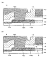
- FIG. 1A is a top view illustrating an example of a transistor.
- FIGS. 1B and 1C are cross-sectional views illustrating an example of a transistor.
- FIGS. 2A and 2B are cross-sectional views illustrating an example of a transistor.
- FIG. 3A is a top view illustrating an example of a transistor.
- FIGS. 3B and 3C are cross-sectional views illustrating an example of a transistor.
- FIGS. 4A to 4C are cross-sectional views illustrating an example of a transistor.
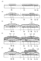
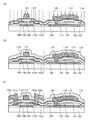
- 5A to 5E are cross-sectional views illustrating an example of a method for manufacturing a transistor.
- 6A and 6B are cross-sectional views illustrating an example of a method for manufacturing a transistor.
- FIGS. 1A is a top view illustrating an example of a transistor.
- FIGS. 1B and 1C are cross-sectional views illustrating an example of a transistor.
- FIGS. 2A and 2B are cross-sectional views
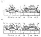
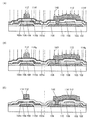
- FIGS. 10A to 10C are top views illustrating an example of a display device.
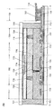
- FIG. 11 is a cross-sectional view illustrating an example of a display device.
- FIG. 12 is a cross-sectional view illustrating an example of a display device.
- FIG. 13 is a cross-sectional view illustrating an example of a display device.
- FIG. 14 is a cross-sectional view illustrating an example of a display device.
- FIG. 15A is a block diagram illustrating an example of a display device.
- FIGS. 15B and 15C are circuit diagrams each illustrating an example of a display device.
- FIGS. 16A, 16C, and 16D are circuit diagrams illustrating an example of a display device.
- FIG. 16B is a timing chart of the display device.
- FIGS. 17A and 17B are diagrams illustrating an example of a display module.
- 18A and 18B illustrate an example of an electronic device.
- FIGS. 19A to 19D illustrate an example of an electronic device.
- 20A to 20E illustrate an example of an electronic device.
- FIGS. 21A to 21F illustrate an example of an electronic device.
- FIG. 22 is a graph illustrating an etching rate of the metal oxide film according to the first embodiment.
- FIGS. 22 is a graph illustrating an etching rate of the metal oxide film according to the first embodiment.
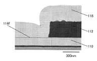
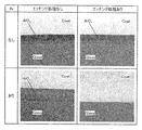
- FIG. 23A and 23B are cross-sectional observation photographs of the sample according to Example 1.
- FIG. FIG. 24 is a graph illustrating electric characteristics of the transistor according to the first embodiment.
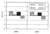
- FIG. 25 is a graph illustrating reliability evaluation results of the transistor according to the first embodiment.
- FIGS. 26A to 26D are graphs showing electric characteristics of the transistor according to the second embodiment.
- FIG. 27 is a graph illustrating reliability evaluation results of the transistor according to the second embodiment.
- FIG. 28 is a cross-sectional observation photograph of the sample according to Example 2.
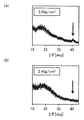
- FIGS. 29A and 29B are graphs showing the results of structural analysis and the film density of the sample according to Example 3.
- FIG. 30 is a cross-sectional observation photograph of the sample according to Example 3.
- FIG. 31 is a cross-sectional observation photograph of the sample according to Example 3.
- film and the word “layer” can be interchanged with each other depending on circumstances or conditions.
- conductive layer can be changed to the term “conductive film”.
- insulating film can be changed to the term “insulating layer”.
- the channel length direction of a transistor refers to one of directions parallel to a straight line connecting the source region and the drain region at the shortest distance. That is, the channel length direction corresponds to one of the directions of current flowing through the semiconductor layer when the transistor is on.
- the channel width direction refers to a direction orthogonal to the channel length direction. Note that the channel length direction and the channel width direction may not be determined to be one depending on the structure and shape of the transistor.
- off-state current refers to a drain current when a transistor is in an off state (also referred to as a non-conductive state or a cut-off state) unless otherwise specified.
- the off state means a state in which the voltage V gs between the gate and the source is lower than the threshold voltage V th in an n-channel transistor (higher than V th in a p-channel transistor).
- a semiconductor layer is formed, a gate insulating layer is formed over the semiconductor layer, a metal oxide layer is formed over the gate insulating layer, and the semiconductor layer is formed over the metal oxide layer.
- a first element is supplied (also referred to as addition or implantation) through a metal oxide layer and a gate insulating layer to a region of the semiconductor layer where the gate electrode does not overlap with the first element. .
- the first element is supplied to the semiconductor layer through the metal oxide layer and the gate insulating layer in this order.
- the layer in which the first element enters first is the most susceptible to damage. Accordingly, by providing the metal oxide layer over the gate insulating layer, the first element first enters the metal oxide layer, so that damage to the gate insulating layer and the semiconductor layer can be reduced. Thus, the reliability of the transistor can be improved.
- the semiconductor layer preferably contains a metal oxide.
- a case where the semiconductor layer contains a metal oxide will be mainly described.
- first heat treatment is preferably performed.
- oxygen be supplied from the gate insulating layer to the semiconductor layer.
- the gate insulating layer preferably contains an oxide. It is preferable that the metal oxide layer does not easily transmit oxygen. Accordingly, release of oxygen contained in the gate insulating layer to the metal oxide layer side can be suppressed, and supply of the oxygen to the semiconductor layer can be promoted. Therefore, oxygen vacancies in the semiconductor layer can be compensated, and the reliability of the transistor can be increased.
- a gate electrode is formed, and the first element is supplied to the semiconductor layer using the gate electrode as a mask, whereby a pair of low-resistance regions can be formed in the semiconductor layer. That is, the semiconductor layer is formed so as to have a channel formation region overlapping with the gate electrode and a pair of low-resistance regions sandwiching the channel formation region.
- the first element is, for example, phosphorus, boron, magnesium, aluminum, or silicon.
- the metal oxide layer does not easily transmit hydrogen and water. Accordingly, it is possible to suppress the release of hydrogen and water contained in the gate electrode to the metal oxide layer side, and to suppress the diffusion of the hydrogen and water into the semiconductor layer. Therefore, an increase in carrier density in the channel formation region of the semiconductor layer can be suppressed. When the number of oxygen vacancies in the channel formation region of the semiconductor layer is small and the carrier density is low, the off-state current of the transistor can be significantly reduced and the reliability of the transistor can be increased.
- the metal oxide layer is processed into an island shape using the gate electrode as a mask, it is preferable to process the metal oxide layer after supplying the first element to the semiconductor layer.
- the first element by supplying the first element to the semiconductor layer through the metal oxide layer, damage to the semiconductor layer and the gate insulating layer can be reduced.
- the first element when the first element is supplied to the semiconductor layer, the first element can be supplied to the metal oxide layer.
- the etching rate of the metal oxide layer can be increased. Accordingly, the etching rate of the metal oxide layer can be different between a portion overlapping the gate electrode and a portion not overlapping the gate electrode. Therefore, a shape defect of the metal oxide layer due to etching can be suppressed.
- the metal oxide layer may be difficult to process depending on the material and the forming conditions. In that case, it is preferable that the second element be supplied to the metal oxide layer and then processed. By supplying the second element to lower the crystallinity of the metal oxide layer, the processing of the metal oxide layer becomes easy.
- the second element is, for example, silicon, phosphorus, argon, krypton, xenon, arsenic, gallium, or germanium.
- the element supply step of the first element and the supply step of the second element there is no limitation on the order of the supply step of the first element and the supply step of the second element.
- the element supply step may be performed only once.
- an aluminum oxide film can be used for the metal oxide layer.
- the metal oxide layer For example, by adding argon to an aluminum oxide film, the aluminum oxide film is easily etched.
- the metal oxide layer and the semiconductor layer preferably have the same metal oxide.
- the metal oxide layer is preferably processed by wet etching.
- wet etching By using wet etching, etching of the gate insulating layer simultaneously with the metal oxide layer can be suppressed. Accordingly, a decrease in the thickness of the gate insulating layer can be suppressed, and the thickness of the gate insulating layer can be made uniform.
- second heat treatment may be performed.
- the first heat treatment is preferably performed at a relatively high temperature (for example, 350 ° C.) in order to sufficiently supply oxygen from the gate insulating layer to the semiconductor layer.
- a relatively high temperature for example, 350 ° C.
- oxygen contained in a channel formation region of the semiconductor layer or the gate insulating layer is reduced. May be diffused into the low resistance region or the gate electrode. Therefore, it is preferable that the second heat treatment be performed at a lower temperature than the first heat treatment.
- the first element can be supplied to the gate insulating layer.
- the first element is mainly supplied to a portion of the gate insulating layer which overlaps with the low-resistance region of the semiconductor layer, and the first element is supplied to a portion which overlaps with the channel formation region of the semiconductor layer. Is difficult to supply the first element. Therefore, in the second heat treatment, oxygen is supplied from the gate insulating layer to the channel formation region, so that oxygen vacancies in the channel formation region are compensated.
- oxygen is hardly supplied from the gate insulating layer, so that the electric resistance does not easily increase.
- FIG. 1A is a top view of the transistor 100.
- FIG. 1B is a cross-sectional view taken along dashed-dotted line A1-A2 in FIG.
- FIG. 1C is a cross-sectional view taken along dashed-dotted line B1-B2 in FIG.
- the direction of the dashed line A1-A2 corresponds to the channel length direction
- the direction of the dashed line B1-B2 corresponds to the channel width direction.
- FIG. 1A some components (eg, a gate insulating layer) of the transistor 100 are not illustrated.
- a top view of the transistor is omitted in some of the drawings as in FIG.
- the transistor 100 includes an insulating layer 103, an island-shaped semiconductor layer 108, a gate insulating layer 110, a metal oxide layer 114, a gate electrode 112, and an insulating layer 118.
- the insulating layer 103 is provided over the substrate 102.
- the semiconductor layer 108 is provided over the insulating layer 103.
- the gate insulating layer 110 is in contact with the upper surface of the insulating layer 103 and the upper surface and side surfaces of the semiconductor layer 108.
- the metal oxide layer 114 is provided over the gate insulating layer 110.
- the metal oxide layer 114 has a portion that overlaps with the semiconductor layer 108 with the gate insulating layer 110 interposed therebetween.
- the gate electrode 112 is provided over the metal oxide layer 114.
- the gate electrode 112 has a portion which overlaps with the semiconductor layer 108 with the gate insulating layer 110 and the metal oxide layer 114 interposed therebetween.
- the insulating layer 118 is provided to cover the upper surface of the gate insulating layer 110, the side surfaces of the metal oxide layer 114, and the upper surface of the gate electrode 112.
- the transistor 100 is a top-gate transistor including a gate electrode 112 over a semiconductor layer 108.
- the transistor 100 may include a conductive layer 120a and a conductive layer 120b over the insulating layer 118.
- One of the conductive layers 120a and 120b functions as a source electrode, and the other functions as a drain electrode.
- the conductive layer 120a and the conductive layer 120b are electrically connected to a low-resistance region 108n described below through an opening 141a or an opening 141b provided in the insulating layer 118 and the gate insulating layer 110, respectively.
- the semiconductor layer 108 preferably includes a metal oxide having semiconductor characteristics (hereinafter, also referred to as an oxide semiconductor).
- the semiconductor layer 108 has a region overlapping with the gate electrode 112 and a pair of low-resistance regions 108n sandwiching the region.
- a region of the semiconductor layer 108 overlapping with the gate electrode 112 functions as a channel formation region where a channel of the transistor 100 can be formed.
- the pair of low-resistance regions 108n functions as a source region and a drain region of the transistor 100.
- the low-resistance region 108n can also be referred to as a region having a lower resistance than the channel formation region, a region with a high carrier concentration, a region with a high oxygen defect density, a region with a high impurity concentration, or an n-type region.
- the low resistance region 108n is a region including one or more impurity elements.
- the impurity element include hydrogen, boron, carbon, nitrogen, fluorine, phosphorus, sulfur, arsenic, aluminum, magnesium, silicon, and a rare gas (such as helium, neon, argon, krypton, and xenon).
- the pair of low resistance regions 108n preferably contains boron, phosphorus, aluminum, magnesium, or silicon, and more preferably contains boron or phosphorus.
- part of the impurity element included in the low-resistance region 108n may be diffused to a channel formation region due to an influence of heat applied in the manufacturing process or the like.
- the concentration of the impurity element in the channel formation region is preferably one-tenth or less, more preferably one-hundredth or less, the concentration of the impurity element in the low-resistance region 108n.
- the gate insulating layer 110 has a region in contact with a channel formation region of the semiconductor layer 108 and overlapping with the gate electrode 112.
- the gate insulating layer 110 has a region which is in contact with the pair of low-resistance regions 108n of the semiconductor layer 108 and does not overlap with the gate electrode 112.
- the gate insulating layer 110 preferably includes an oxide.
- the gate insulating layer 110 is preferably an oxide film from which oxygen can be released by heating.
- heat treatment is performed before the formation of the gate electrode 112 and the supply of the impurity element to the semiconductor layer 108, so that oxygen is supplied from the gate insulating layer 110 to the semiconductor layer 108.
- heat treatment may be performed after formation of the gate electrode 112 and supply of the impurity element to the semiconductor layer 108.
- oxygen contained in the channel formation region of the semiconductor layer 108 may diffuse into the low-resistance region 108n and the gate electrode 112. Further, oxygen may be supplied from the gate insulating layer 110 to the low-resistance region 108n.
- the carrier density may decrease and the electric resistance may increase.
- the impurity element be contained in a region of the gate insulating layer 110 which is in contact with the pair of low-resistance regions 108n, that is, a region which does not overlap with the gate electrode 112.
- the region of the gate insulating layer 110 which does not overlap with the gate electrode 112 preferably has a region where the impurity concentration is higher than the region of the gate insulating layer 110 overlapping with the gate electrode 112 and lower than the low resistance region 108n.
- the insulating layer 103 and the gate insulating layer 110 which are in contact with the channel formation region of the semiconductor layer 108 preferably include an oxide.
- an oxide film such as a silicon oxide film, a silicon oxynitride film, or an aluminum oxide film can be used.
- oxygen released from the insulating layer 103 or the gate insulating layer 110 due to heat treatment or the like in the manufacturing process of the transistor 100 is supplied to the channel formation region of the semiconductor layer 108 to reduce oxygen vacancies in the semiconductor layer 108. it can.
- FIG. 2A is an enlarged cross-sectional view of a region P surrounded by a dashed line in FIG.
- the gate insulating layer 110 has a region 110d containing the above-described impurity element.
- the region 110d is located at least at the interface with the low-resistance region 108n or in the vicinity thereof.
- the region 110d is located at or near an interface with the insulating layer 103 in a region where the semiconductor layer 108 and the gate electrode 112 are not provided.
- the region 110d is preferably not provided in a portion of the semiconductor layer 108 which is in contact with a channel formation region.
- the insulating layer 103 includes a region 103d containing the above-described impurity element at or near an interface in contact with the gate insulating layer 110. As illustrated in FIG. 2A, the region 103d may be provided at an interface in contact with the low-resistance region 108n or in the vicinity thereof. At this time, the impurity concentration in a portion overlapping with the low-resistance region 108n is lower than the concentration in contact with the gate insulating layer 110.
- the impurity concentration in the low-resistance region 108n has a concentration gradient such that the concentration is higher as the position is closer to the gate insulating layer 110.
- the concentration is uniform over the entire low resistance region 108n
- the total amount of the impurity elements in the low resistance region 108n can be reduced, so that the impurity element diffuses into the channel formation region due to heat or the like during the manufacturing process. The amount of impurities that can be obtained can be kept low.
- the impurity concentration in the region 110d preferably has a concentration gradient such that the concentration increases as the position approaches the low-resistance region 108n.
- the gate insulating layer 110 to which the oxide film capable of releasing oxygen by heating is applied the release of oxygen can be suppressed in the region 110d containing the above-described impurity element as compared with the other regions. Therefore, the region 110d of the gate insulating layer 110 located at or near the interface with the low-resistance region 108n functions as a blocking layer for oxygen, and can effectively reduce oxygen supplied to the low-resistance region 108n. .
- the supply of the impurity element is performed at least to the semiconductor layer 108 using the gate electrode 112 as a mask. Further, the impurity element is preferably supplied also to the gate insulating layer 110. This allows the region 110d to be formed in a self-aligned manner at the same time as the formation of the low resistance region 108n.
- the region 110 d is exaggerated to show that the portion of the gate insulating layer 110 with a high impurity concentration is located at or near the interface with the semiconductor layer 108. Although a hatching pattern is shown only in the vicinity of the semiconductor layer 108 in the middle, the impurity element is included in the entire gate insulating layer 110 in the thickness direction.
- the supply of the impurity element is preferably performed by a plasma ion doping method or an ion implantation method. In these methods, since the depth at which ions are added is easily adjusted, ions can be easily added to a region including the gate insulating layer 110 and the semiconductor layer 108.
- the supply condition of the impurity element be set so that the impurity concentration in the region of the semiconductor layer 108 on the gate insulating layer 110 side or in the interface between the semiconductor layer 108 and the gate insulating layer 110 or in the vicinity thereof is the highest. .
- an appropriate concentration of the impurity element can be supplied to both the semiconductor layer 108 and the gate insulating layer 110 in one step.
- the contact resistance between the low-resistance region 108n and the source electrode or the drain electrode can be reduced by supplying the impurity element at a high concentration over the low-resistance region 108n to reduce the resistance.
- the diffusibility of oxygen in this portion is reduced and oxygen in the gate insulating layer 110 is reduced to a low-resistance region. Diffusion to the 108n side can be further suppressed.
- Each of the low resistance region 108n and the region 110d has an impurity concentration of 1 ⁇ 10 19 atoms / cm 3 to 1 ⁇ 10 23 atoms / cm 3 , preferably 5 ⁇ 10 19 atoms / cm 3 to 5 ⁇ 10 22 atoms / cm 3. It is preferable to include a region having a size of not more than cm 3 , more preferably not less than 1 ⁇ 10 20 atoms / cm 3 and not more than 1 ⁇ 10 22 atoms / cm 3 .
- the low-resistance region 108n include a portion having a higher impurity concentration than the region 110d of the gate insulating layer 110, because the electric resistance of the low-resistance region 108n can be further reduced.
- the concentration of the impurities contained in the low resistance region 108n and the region 110d is determined by, for example, a secondary ion mass spectrometry (SIMS: Secondary Ion Mass Spectrometry) or an X-ray photoelectron spectroscopy (XPS: X-ray Photoelectron Spectroscopy). Can be analyzed by When XPS analysis is used, the concentration distribution in the depth direction can be known by combining ion sputtering from the front side or the back side with XPS analysis.
- SIMS Secondary Ion Mass Spectrometry
- XPS X-ray Photoelectron Spectroscopy
- the impurity element exists in a state bonded to oxygen in the semiconductor layer 108. That is, when the impurity element deprives oxygen in the semiconductor layer 108, oxygen vacancies are generated in the semiconductor layer 108, and the oxygen vacancies are combined with hydrogen in the film to generate carriers. Further, since the impurity element in the semiconductor layer 108 is stably present in an oxidized state, the impurity element is not easily desorbed by heat or the like during the process, and a stable low-resistance region 108n with a low electric resistance can be realized.
- the impurity element exists in the gate insulating layer 110 in a state bonded to oxygen as in the semiconductor layer 108.
- oxygen and the impurity element are combined and stabilized, oxygen is hardly desorbed in a region including the impurity element even when heating is performed, so that oxygen is hardly diffused to another layer.
- oxygen can be supplied to the channel formation region while suppressing supply of oxygen from the gate insulating layer 110 to the low-resistance region 108n. Therefore, oxygen vacancies in the channel formation region can be reduced while preventing the resistance of the low resistance region 108n from increasing. As a result, a transistor with favorable electric characteristics and high reliability can be realized.
- an element which is combined with oxygen in the semiconductor layer 108 and the gate insulating layer 110 to be stabilized is preferably used.
- an element whose oxide can exist as a solid in a standard state is preferable to use.
- Particularly preferred elements include a rare gas, a typical nonmetallic element other than hydrogen, a typical metal element, and a transition metal element, with boron, phosphorus, aluminum, magnesium, and silicon being particularly preferred.
- boron contained in the low-resistance region 108n and the region 110d may exist in a state of being bonded to oxygen. This can be confirmed by observing a spectrum peak due to B 2 O 3 bonding in the XPS analysis. Further, in the XPS analysis, the peak intensity due to the state where the boron element exists alone is not observed, or the peak intensity becomes extremely small to such an extent that it is buried in the background noise at the lower limit of measurement.
- the metal oxide layer 114 is formed using a material that does not easily transmit oxygen and hydrogen.
- the metal oxide layer 114 has a function of preventing oxygen contained in the gate insulating layer 110 from diffusing to the gate electrode 112 side.
- the metal oxide layer 114 has a function of preventing hydrogen and water contained in the gate electrode 112 from diffusing to the gate insulating layer 110 side. It is preferable that the metal oxide layer 114 be formed using a material that does not easily transmit oxygen and hydrogen than the gate insulating layer 110 at least.
- the provision of the metal oxide layer 114 prevents diffusion of oxygen from the gate insulating layer 110 to the gate electrode 112 even when a metal material such as aluminum or copper which easily absorbs oxygen is used for the gate electrode 112. Can be prevented. Further, even when the gate electrode 112 contains hydrogen, diffusion of hydrogen from the gate electrode 112 to the semiconductor layer 108 through the gate insulating layer 110 can be prevented. As a result, the carrier density in the channel formation region of the semiconductor layer 108 can be extremely low.
- the metal oxide layer 114 may be either an insulating layer or a conductive layer. When the metal oxide layer 114 is an insulating layer, the metal oxide layer 114 can be referred to as part of the gate insulating layer 110. When the metal oxide layer 114 is a conductive layer, the metal oxide layer 114 can be referred to as a part of the gate electrode 112.
- an insulating material having a higher dielectric constant than silicon oxide be used for the metal oxide layer 114.
- an aluminum oxide film, a hafnium oxide film, a hafnium aluminate film, or the like is preferably used because a driving voltage can be reduced.
- a conductive oxide such as indium oxide, indium tin oxide (ITO), or indium tin oxide containing silicon (ITSO) can be used.
- ITO indium tin oxide
- ITSO indium tin oxide containing silicon
- a conductive oxide containing indium is preferable because of its high conductivity.
- the metal oxide layer 114 be formed using an oxide material containing one or more of the same elements as the semiconductor layer 108.
- an oxide semiconductor material that can be used for the semiconductor layer 108 is preferably used.
- the metal oxide layer 114 is preferably formed using a sputtering apparatus.
- oxygen can be supplied to the gate insulating layer 110 and the semiconductor layer 108 in an atmosphere containing oxygen gas.
- the manufacturing process of the transistor 100 includes a step of forming the metal oxide layer 114 in an island shape. Further, even when the metal oxide layer 114 is an insulating layer, the metal oxide layer 114 can be formed in an island shape. At this time, processing may be difficult depending on the material and the processing method.
- an impurity element is supplied to the semiconductor layer 108 through the metal oxide layer 114. Accordingly, the impurity element is also supplied to the metal oxide layer 114, and the etching rate of the metal oxide layer 114 can be increased. Therefore, the etching rate of the metal oxide layer 114 can be different between a portion overlapping the gate electrode 112 and a portion not overlapping. Therefore, a portion of the metal oxide layer 114 that overlaps with the gate electrode 112 is hardly etched, and a shape defect of the metal oxide layer 114 can be suppressed. In addition, coverage of the insulating layer 118 can be improved, and poor coverage can be suppressed.
- the gate electrode 112 and the metal oxide layer 114 are processed so that their top shapes substantially match each other.
- the island-shaped metal oxide layer 114 can be formed by processing using the gate electrode 112 as a mask.
- the upper surfaces have substantially the same shape means that at least a part of the outline overlaps between the stacked layers. For example, this includes the case where the lower layer is processed using the upper layer as a mask, and the case where the upper layer and the lower layer are processed with the same mask pattern or a part of the same mask pattern. However, the contours do not strictly overlap, and the upper layer may be located inside the lower layer, or the upper layer may be located outside the lower layer. In this case, too, the upper surface shapes are substantially matched.
- the insulating layer 118 functions as a protective layer for protecting the transistor 100.
- the insulating layer 118 preferably has a function of preventing oxygen released from the gate insulating layer 110 from being diffused to the outside.
- an inorganic insulating material such as an oxide or a nitride can be used.
- an inorganic insulating material such as silicon nitride, silicon nitride oxide, silicon oxynitride, aluminum oxide, aluminum oxynitride, aluminum nitride, hafnium oxide, or hafnium aluminate can be used.
- FIG. 3A is a top view of the transistor 100A.
- FIG. 3B is a cross-sectional view taken along dashed-dotted line A1-A2 in FIG.
- FIG. 3C is a cross-sectional view taken along dashed-dotted line B1-B2 in FIG.
- the direction of the dashed line A1-A2 corresponds to the channel length direction
- the direction of the dashed line B1-B2 corresponds to the channel width direction.
- the transistor 100A is different from the transistor 100 in that a conductive layer 106 is provided between the substrate 102 and the insulating layer 103.
- the conductive layer 106 has a region overlapping with the semiconductor layer 108 and the gate electrode 112.
- the conductive layer 106 has a function as a first gate electrode (also referred to as a bottom gate electrode), and the gate electrode 112 has a function as a second gate electrode (also referred to as a top gate electrode).
- the insulating layer 103 functions as a first gate insulating layer
- part of the gate insulating layer 110 functions as a second gate insulating layer.
- a portion of the semiconductor layer 108 that overlaps with at least one of the gate electrode 112 and the conductive layer 106 functions as a channel formation region. Note that a portion of the semiconductor layer 108 that overlaps with the gate electrode 112 may be referred to as a channel formation region hereinafter for ease of description. A channel can be formed also in the region including the region 108n).
- the conductive layer 106 is electrically connected to the gate electrode 112 through the metal oxide layer 114, the gate insulating layer 110, and the opening 142 provided in the insulating layer 103. It may be connected. Thus, the same potential can be applied to the conductive layer 106 and the gate electrode 112.
- a material similar to that of the gate electrode 112, the conductive layer 120a, or the conductive layer 120b can be used. It is particularly preferable to use a material containing copper for the conductive layer 106 because wiring resistance can be reduced.
- the gate electrode 112 and the conductive layer 106 protrude outside the edge of the semiconductor layer 108 in the channel width direction.
- the entire semiconductor layer 108 in the channel width direction is covered with the gate electrode 112 and the conductive layer 106 with the gate insulating layer 110 and the insulating layer 103 interposed therebetween. .
- the semiconductor layer 108 can be electrically surrounded by an electric field generated by the pair of gate electrodes. At this time, it is particularly preferable to apply the same potential to the conductive layer 106 and the gate electrode 112. Thus, an electric field for inducing a channel can be effectively applied to the semiconductor layer 108, so that the on-state current of the transistor 100A can be increased. Therefore, the transistor 100A can be miniaturized.
- a structure in which the gate electrode 112 and the conductive layer 106 are not connected may be employed.
- a constant potential may be applied to one of the pair of gate electrodes, and a signal for driving the transistor 100A may be applied to the other.
- the threshold voltage when the transistor 100A is driven by the other electrode can be controlled by the potential applied to one electrode.
- a semiconductor device of one embodiment of the present invention which includes a transistor and a capacitor, is described with reference to FIGS. Specifically, an example is described in which the transistor and the capacitor are formed over one surface using the semiconductor layer 108c containing an impurity as one electrode of the capacitor.
- the capacitor 130A illustrated in FIG. 4A is provided side by side with the transistor 100 (FIGS. 1A to 1C).
- the capacitor 130A illustrated in FIG. 4B is provided side by side with the transistor 100A (FIGS. 3A to 3C).
- the capacitor 130A has a structure in which the gate insulating layer 110 and the insulating layer 118 functioning as a dielectric are provided between the semiconductor layer 108c and the conductive layer 120b.
- the semiconductor layer 108c is provided on the same plane as the semiconductor layer 108.
- the semiconductor layer 108c can be formed by processing the same metal oxide film as the semiconductor layer 108 and supplying the same impurity element as the low-resistance region 108n.
- the capacitor 130A can be manufactured at the same time as the transistor without increasing the number of manufacturing steps.
- the capacitor 130B illustrated in FIG. 4C is provided side by side with the transistor 100A (FIGS. 3A to 3C).
- the capacitor 130B has a structure in which the insulating layer 103 serving as a dielectric is provided between the conductive layer 106c and the semiconductor layer 108c.
- the conductive layer 106c is provided on the same surface as the conductive layer 106.
- the conductive layer 106c can be formed by processing the same conductive film as the conductive layer 106.
- the capacitor 130B can be smaller than that of the capacitor 130A, the capacitor can have a larger capacity.
- the substrate 102 there is no particular limitation on the material or the like of the substrate 102, but it is necessary that the substrate have at least enough heat resistance to withstand heat treatment performed later.
- a single crystal semiconductor substrate using silicon or silicon carbide, a polycrystalline semiconductor substrate, a compound semiconductor substrate such as silicon germanium, an SOI substrate, a glass substrate, a ceramic substrate, a quartz substrate, a sapphire substrate, or the like is used as the substrate 102. Is also good.
- a substrate provided with a semiconductor element over these substrates may be used as the substrate 102.
- a flexible substrate may be used as the substrate 102, and the transistor 100 and the like may be formed directly over the flexible substrate.
- a separation layer may be provided between the substrate 102 and the transistor 100 or the like. The peeling layer can be used to complete a part or the whole of a semiconductor device thereon, separate it from the substrate 102, and transfer it to another substrate. In that case, the transistor 100 and the like can be transferred to a substrate having low heat resistance or a flexible substrate.
- the insulating layer 103 can be formed using a single layer or a stacked layer of an oxide insulating film or a nitride insulating film. Note that at least a region of the insulating layer 103 which is in contact with the semiconductor layer 108 is preferably formed using an oxide insulating film in order to improve interface characteristics with the semiconductor layer 108. Further, a film which releases oxygen by heating is preferably used for the insulating layer 103.
- the insulating layer 103 for example, silicon oxide, silicon oxynitride, silicon nitride oxide, silicon nitride, aluminum oxide, hafnium oxide, gallium oxide, Ga-Zn oxide, or the like may be used, and a single layer or a stacked layer can be provided.
- pretreatment such as oxygen plasma treatment is performed on a surface which is in contact with the semiconductor layer 108, Alternatively, it is preferable to oxidize near the surface.
- the gate electrode 112, the conductive layer 106 serving as a gate electrode, and the conductive layers 120a and 120b serving as source and drain electrodes are formed using chromium, copper, aluminum, gold, silver, zinc, molybdenum, tantalum, titanium,
- Each of the metal elements can be formed using a metal element selected from tungsten, manganese, nickel, iron, and cobalt, an alloy including the above-described metal element as a component, an alloy in which the above-described metal elements are combined, or the like.
- the gate electrode 112, the conductive layer 106, the conductive layer 120a, and the conductive layer 120b are each formed of an In-Sn oxide, an In-W oxide, an In-W-Zn oxide, an In-Ti oxide, an In-Ti oxide.
- An oxide conductor (OC: Oxide Conductor) such as a -Sn oxide, an In-Zn oxide, an In-Sn-Si oxide, or an In-Ga-Zn oxide, or a metal oxide film can also be used.
- an oxide conductor OC
- each of the gate electrode 112 and the conductive layer 106 may have a stacked structure of a conductive film containing the oxide conductor (metal oxide) and a conductive film containing a metal or an alloy.
- a conductive film containing a metal or an alloy wiring resistance can be reduced.
- a conductive film containing an oxide conductor is preferably applied to a side of the gate electrode 112 which is in contact with the gate insulating layer 110 or a side of the conductive layer 106 which is in contact with the insulating layer 103.
- the gate electrode 112, the conductive layer 106, the conductive layer 120a, and the conductive layer 120b each include, among the above metal elements, any one or more selected from among titanium, tungsten, tantalum, and molybdenum. It is preferred to have. In particular, it is preferable to use a tantalum nitride film.
- the tantalum nitride film has conductivity, has a high barrier property against copper, oxygen, or hydrogen, and emits little hydrogen from itself. It is suitable as a conductive film in the vicinity of the layer 108.
- An insulating layer containing one or more of a magnesium film, a lanthanum oxide film, a cerium oxide film, and a neodymium oxide film can be used. Note that the gate insulating layer 110 is not limited to a single layer and may have a stacked structure of two or more layers.
- At least a region of the gate insulating layer 110 which is in contact with the semiconductor layer 108 is preferably an oxide insulating film, and more preferably has a region containing oxygen in excess of the stoichiometric composition.
- the gate insulating layer 110 is an insulating film that can release oxygen.
- the gate insulating layer 110 is formed in an oxygen atmosphere, heat treatment, plasma treatment, or the like is performed on the formed gate insulating layer 110 in an oxygen atmosphere. Oxygen can be supplied into the gate insulating layer 110 by forming an oxide film in an atmosphere or the like.
- the gate insulating layer 110 a material such as hafnium oxide having a higher relative dielectric constant than silicon oxide or silicon oxynitride can be used. This makes it possible to increase the thickness of the gate insulating layer 110 and suppress a leak current due to a tunnel current.
- hafnium oxide having crystallinity is preferable because it has a higher relative dielectric constant than amorphous hafnium oxide.
- the semiconductor layer 108 preferably includes an oxide semiconductor.
- the semiconductor layer 108 may include silicon.
- Examples of silicon include amorphous silicon and crystalline silicon (low-temperature polysilicon, single crystal silicon, and the like).
- the semiconductor layer 108 includes, for example, indium and M (M is gallium, aluminum, silicon, boron, yttrium, tin, copper, vanadium, beryllium, titanium, iron, nickel, germanium, zirconium, molybdenum, lanthanum, cerium, or neodymium. , One or more selected from hafnium, tantalum, tungsten, and magnesium) and zinc.
- M is preferably one or more selected from aluminum, gallium, yttrium, and tin.
- an oxide containing indium (In), gallium (Ga), and zinc (Zn) (also referred to as IGZO) is preferably used.
- the sputtering target used for forming the In-M-Zn oxide preferably has an atomic ratio of In equal to or higher than that of M.
- the atomic ratio of the semiconductor layer 108 to be formed includes a variation of ⁇ 40% of the atomic ratio of the metal element included in the sputtering target.
- oxygen vacancies that can be formed in the semiconductor layer 108 are described.
- Oxygen vacancies formed in the semiconductor layer 108 are problematic because they affect transistor characteristics. For example, when oxygen vacancies are formed in the semiconductor layer 108, hydrogen is bonded to the oxygen vacancies and can serve as a carrier supply source. When a carrier supply source is generated in the semiconductor layer 108, a change in electric characteristics of the transistor 100, typically, a shift in threshold voltage occurs. Therefore, in the semiconductor layer 108, it is preferable that the number of oxygen vacancies be small.
- the insulating film in the vicinity of the semiconductor layer 108 is a configuration including.
- oxygen vacancies in the semiconductor layer 108 can be reduced.
- a metal oxide containing nitrogen may be collectively referred to as a metal oxide (metal oxide). Further, a metal oxide containing nitrogen may be referred to as metal oxynitride. For example, a metal oxide containing nitrogen such as zinc oxynitride (ZnON) may be used for the semiconductor layer.
- metal oxide metal oxide
- ZnON zinc oxynitride
- CAAC c-axis @ aligned crystal
- CAC Cloud-Aligned @ Composite
- CAC Cloud-Aligned @ Composite
- OS can be used for the semiconductor layer.
- the CAC-OS or CAC-metal oxide has a conductive function in part of a material, an insulating function in part of the material, and a semiconductor function as a whole of the material.
- a conductive function is a function of flowing electrons (or holes) serving as carriers
- an insulating function is a function of flowing electrons (carriers). This is a function that does not flow.
- the CAC-OS or CAC-metal oxide includes a conductive region and an insulating region.
- the conductive region has the above-described conductive function
- the insulating region has the above-described insulating function.
- a conductive region and an insulating region are separated at a nanoparticle level in a material.
- the conductive region and the insulating region may be unevenly distributed in the material.
- the conductive region is blurred at the periphery and observed in a cloud shape.
- the conductive region and the insulating region are each dispersed in a material in a size of 0.5 nm to 10 nm, preferably 0.5 nm to 3 nm. There is.
- CAC-OS or CAC-metal oxide includes components having different band gaps.
- CAC-OS or CAC-metal oxide includes a component having a wide gap due to an insulating region and a component having a narrow gap due to a conductive region.
- the carrier when the carrier flows, the carrier mainly flows in the component having the narrow gap.
- the component having the narrow gap acts complementarily to the component having the wide gap, and the carrier also flows to the component having the wide gap in conjunction with the component having the narrow gap. Therefore, in the case where the CAC-OS or CAC-metal oxide is used for a channel formation region of a transistor, high current driving force, that is, a high on-state current and high field-effect mobility can be obtained when the transistor is on.
- CAC-OS or CAC-metal oxide can be referred to as a matrix composite or a metal matrix composite.
- An oxide semiconductor is classified into a single crystal oxide semiconductor and a non-single-crystal oxide semiconductor.
- a non-single-crystal oxide semiconductor for example, CAAC-OS (c-axis aligned crystalline oxide semiconductor), polycrystalline oxide semiconductor, nc-OS (nanocrystalline oxide semiconductor), and pseudo-amorphous oxide semiconductor (a-like) OS: amorphous-like oxide semiconductor (OS), an amorphous oxide semiconductor, or the like.
- the CAAC-OS has a c-axis orientation and a crystal structure in which a plurality of nanocrystals are connected in an ab plane direction and has a strain.
- the strain refers to a region where the orientation of the lattice arrangement changes between a region where the lattice arrangement is uniform and a region where another lattice arrangement is uniform in a region where a plurality of nanocrystals are connected.
- the nanocrystal is based on a hexagon, but is not limited to a regular hexagon and may be a non-regular hexagon.
- distortion may have a lattice arrangement such as a pentagon and a heptagon.
- a clear crystal grain boundary also referred to as a grain boundary
- the CAAC-OS can tolerate distortion because the arrangement of oxygen atoms is not dense in the ab plane direction, or the substitution distance of a metal element changes the bonding distance between atoms. That's why.
- the CAAC-OS is a layered crystal in which a layer containing indium and oxygen (hereinafter, an In layer) and a layer containing elements M, zinc, and oxygen (hereinafter, an (M, Zn) layer) are stacked. It tends to have a structure (also called a layered structure).
- indium and the element M can be replaced with each other, and when the element M in the (M, Zn) layer is replaced with indium, it can also be expressed as an (In, M, Zn) layer. Further, when indium in the In layer is replaced with the element M, it can also be referred to as an (In, M) layer.
- CAAC-OS is a metal oxide with high crystallinity.
- CAAC-OS it is difficult to confirm a clear crystal grain boundary; thus, it can be said that electron mobility due to the crystal grain boundary is hardly reduced.
- CAAC-OS impurities and defects oxygen deficiency (V O:. Oxygen vacancy also referred) etc.) with less metal It can also be called an oxide. Therefore, a metal oxide having a CAAC-OS has stable physical properties. Therefore, a metal oxide including CAAC-OS is resistant to heat and has high reliability.
- the nc-OS has a periodic atomic arrangement in a minute region (for example, a region with a thickness of 1 nm to 10 nm, particularly a region with a size of 1 nm to 3 nm).
- a minute region for example, a region with a thickness of 1 nm to 10 nm, particularly a region with a size of 1 nm to 3 nm.
- the nc-OS may not be distinguished from an a-like @ OS or an amorphous oxide semiconductor depending on an analysis method.
- indium-gallium-zinc oxide which is a kind of metal oxide including indium, gallium, and zinc
- IGZO indium-gallium-zinc oxide
- a smaller crystal for example, the above-described nanocrystal
- a large crystal here, a crystal of several mm or a crystal of several cm.
- it may be structurally stable.
- a-like @ OS is a metal oxide having a structure between an nc-OS and an amorphous oxide semiconductor.
- a-like @ OS has voids or low density regions. That is, a-like @ OS has lower crystallinity than the nc-OS and the CAAC-OS.
- Oxide semiconductors have various structures, and each has different characteristics.
- the oxide semiconductor of one embodiment of the present invention may include two or more of an amorphous oxide semiconductor, a polycrystalline oxide semiconductor, an a-like @ OS, an nc-OS, and a CAAC-OS.
- the metal oxide film functioning as a semiconductor layer can be formed using one or both of an inert gas and an oxygen gas.
- an inert gas an oxygen gas
- an oxygen gas an oxygen gas
- the flow rate ratio of oxygen (oxygen partial pressure) at the time of formation of the metal oxide film is preferably 0% or more and 30% or less, and 5% or more and 30% or less. Is more preferable, and 7% or more and 15% or less are still more preferable.
- the metal oxide preferably has an energy gap of 2 eV or more, more preferably 2.5 eV or more, even more preferably 3 eV or more.
- FIGS. 5 to 9 show cross sections in the channel length direction and the channel width direction at each stage of the transistor manufacturing process.
- a thin film (an insulating film, a semiconductor film, a conductive film, or the like) included in a semiconductor device is formed by a sputtering method, a chemical vapor deposition (CVD) method, a vacuum evaporation method, or a pulsed laser deposition (PLD: Pulsed Laser Deposition).
- CVD chemical vapor deposition
- PLD Pulsed Laser Deposition
- ALD Atomic Layer Deposition
- the CVD method include a plasma enhanced chemical vapor deposition (PECVD) method and a thermal CVD method.
- PECVD plasma enhanced chemical vapor deposition
- thermal CVD there is a metal organic chemical vapor deposition (MOCVD) method.
- thin films constituting semiconductor devices include spin coating, dipping, spray coating, inkjet, dispensing, screen printing, offset printing, doctor knife, slit coating, roll coating, curtain coating. , A knife coat or the like.
- the thin film when a thin film included in a semiconductor device is processed, the thin film can be processed using a photolithography method or the like.
- a thin film may be processed by a nanoimprint method, a sand blast method, a lift-off method, or the like.
- an island-shaped thin film may be directly formed by a film formation method using a shielding mask such as a metal mask.
- the photolithography method there are typically the following two methods.
- One is a method of forming a resist mask on a thin film to be processed, processing the thin film by etching or the like, and removing the resist mask.
- the other is a method of forming a thin film having photosensitivity, performing exposure and development, and processing the thin film into a desired shape.
- light used for exposure can be, for example, i-line (wavelength 365 nm), g-line (wavelength 436 nm), h-line (wavelength 405 nm), or a mixture thereof.
- ultraviolet light, KrF laser light, ArF laser light, or the like can be used.
- the exposure may be performed by a liquid immersion exposure technique.
- extreme ultraviolet light EUV: Extreme-Ultra-violet
- X-ray may be used as light used for exposure.
- an electron beam can be used instead of light used for exposure. It is preferable to use extreme ultraviolet light, X-rays, or an electron beam because extremely fine processing can be performed.
- a photomask is not required.
- etching the thin film For etching the thin film, a dry etching method, a wet etching method, a sand blast method, or the like can be used.
- a conductive film is formed over a substrate 102 and processed by etching, so that a conductive layer 106 serving as a gate electrode is formed.
- treatment for supplying oxygen to the insulating layer 103 may be performed.
- the treatment for supplying oxygen include plasma treatment in an oxygen atmosphere, heat treatment in an oxygen atmosphere, treatment using a plasma ion doping method, treatment using an ion implantation method, and the like.
- a metal oxide film is formed over the insulating layer 103 and processed to form an island-shaped semiconductor layer 108 (FIG. 5B).
- the metal oxide film is preferably formed by a sputtering method using a metal oxide target.
- oxygen gas In forming the metal oxide film, it is preferable to use oxygen gas.
- an inert gas for example, a helium gas, an argon gas, a xenon gas, or the like
- an oxygen flow ratio the higher the proportion of the oxygen gas in the entire deposition gas (hereinafter, also referred to as an oxygen flow ratio) in forming the metal oxide film, the higher the crystallinity of the metal oxide film can be increased, Transistor having a high density can be realized.
- the oxygen flow rate ratio is lower, the crystallinity of the metal oxide film is lower, so that the transistor can have higher on-state current.
- the substrate temperature may be higher than or equal to room temperature and lower than or equal to 200 ° C., preferably, higher than or equal to room temperature and lower than or equal to 140 ° C.
- productivity is preferably increased.
- crystallinity can be reduced.
- a treatment for desorbing water, hydrogen, an organic component, or the like adsorbed on the surface of the insulating layer 103 or a treatment for supplying oxygen into the insulating layer 103 are performed.
- heat treatment can be performed at a temperature of 70 ° C to 200 ° C in a reduced-pressure atmosphere.
- plasma treatment may be performed in an atmosphere containing oxygen.
- organic substances on the surface of the insulating layer 103 can be appropriately removed.
- a metal oxide film is preferably formed continuously without exposing the surface of the insulating layer 103 to the air.
- one or both of a wet etching method and a dry etching method may be used. At this time, part of the insulating layer 103 which does not overlap with the semiconductor layer 108 may be etched and become thinner.
- heat treatment may be performed to remove hydrogen or water in the metal oxide film or the semiconductor layer 108.
- the temperature of the heat treatment can be typically higher than or equal to 150 ° C. and lower than the strain point of the substrate, higher than or equal to 250 ° C. and lower than or equal to 450 ° C., or higher than or equal to higher than or equal to 300 ° C. and lower than or equal to 450 ° C.
- the heat treatment can be performed in an atmosphere containing a rare gas or nitrogen. Alternatively, after heating in the atmosphere, heating may be performed in an atmosphere containing oxygen. Note that it is preferable that hydrogen, water, and the like be not contained in the atmosphere of the heat treatment.
- an electric furnace, an RTA apparatus, or the like can be used. With the use of the RTA apparatus, the heat treatment time can be reduced.
- a gate insulating layer 110 and a metal oxide layer 114f are stacked to cover the insulating layer 103 and the semiconductor layer 108 (FIG. 5C).
- an oxide film such as a silicon oxide film or a silicon oxynitride film is preferably formed by a PECVD method.
- the gate insulating film may be formed by a PECVD method using microwaves.
- the metal oxide layer 114f is preferably formed, for example, in an atmosphere containing oxygen.
- it is preferably formed by a sputtering method in an atmosphere containing oxygen.
- oxygen can be supplied to the gate insulating layer 110 when the metal oxide layer 114f is formed.
- the metal oxide layer 114f is formed by a sputtering method using an oxide target containing a metal oxide similar to that of the semiconductor layer 108, the above method can be employed.
- the metal oxide layer 114f may be formed by a reactive sputtering method using oxygen as a deposition gas and a metal target.
- a reactive sputtering method using oxygen as a deposition gas and a metal target.
- an aluminum oxide film can be formed.
- the ratio of the oxygen flow rate to the total flow rate of the film formation gas introduced into the film formation chamber of the film formation apparatus (oxygen flow ratio) or the oxygen partial pressure in the film formation chamber becomes higher, the gate insulation becomes higher.
- Oxygen provided in layer 110 can be increased.
- the oxygen flow ratio or oxygen partial pressure is, for example, 50% or more and 100% or less, preferably 65% or more and 100% or less, more preferably 80% or more and 100% or less, and further preferably 90% or more and 100% or less.
- it is preferable that the oxygen flow rate is 100% and the oxygen partial pressure is as close as possible to 100%.
- oxygen is preferably supplied from the gate insulating layer 110 to the semiconductor layer 108 by performing heat treatment.
- the heat treatment can be performed at a temperature of 200 ° C to 400 ° C in an atmosphere containing one or more of nitrogen, oxygen, and a rare gas.
- oxygen can be effectively supplied from the gate insulating layer 110 to the semiconductor layer 108.
- the metal oxide layer 114f After the formation of the metal oxide layer 114f, the metal oxide layer 114f, the gate insulating layer 110, and part of the insulating layer 103 are etched, so that an opening 142 reaching the conductive layer 106 is formed.
- the gate electrode 112 to be formed later and the conductive layer 106 can be electrically connected to each other at the opening 142.
- a conductive film 112f to be the gate electrode 112 is formed over the metal oxide layer 114f (FIG. 5D).
- the conductive film 112f is preferably formed by a sputtering method using a metal or alloy sputtering target.
- the conductive film 112f and the conductive layer 106 are connected.
- part of the conductive film 112f is etched to form the gate electrode 112 (FIG. 5E).
- the metal oxide layer 114f and the gate insulating layer 110 cover the upper surface and the side surfaces of the semiconductor layer 108 and the insulating layer 103, the semiconductor layer 108 Part of the insulating layer 103 can be prevented from being etched and thinned.
- the gate electrode 112 As a mask, a process of supplying the impurity element 140 to the metal oxide layer 114f, the gate insulating layer 110, and the semiconductor layer 108 is performed, so that a low-resistance region 108n, a region 110d, and a region 103d are formed. (FIG. 6A). In the region of the semiconductor layer 108, the gate insulating layer 110, and the metal oxide layer 114f which overlaps with the gate electrode 112, the gate electrode 112 serves as a mask and the impurity element 140 is not supplied.
- a plasma ion doping method or an ion implantation method can be preferably used. According to these methods, the concentration profile in the depth direction can be controlled with high accuracy by the ion acceleration voltage and the dose. By using the plasma ion doping method, productivity can be increased. Further, by using an ion implantation method using mass separation, the purity of a supplied impurity element can be increased.
- the interface between the semiconductor layer 108 and the gate insulating layer 110, a portion near the interface in the semiconductor layer 108, or a portion near the interface in the gate insulating layer 110 has the highest concentration.
- the impurity element 140 at an optimum concentration can be supplied to both the semiconductor layer 108 and the gate insulating layer 110 in one process.
- Examples of the impurity element 140 include hydrogen, boron, carbon, nitrogen, fluorine, phosphorus, sulfur, arsenic, aluminum, magnesium, silicon, and a rare gas. It is preferable to use boron, phosphorus, aluminum, magnesium, or silicon as the impurity element 140, and it is more preferable to use boron or phosphorus.
- a gas containing the above impurity element can be used.
- a B 2 H 6 gas, a BF 3 gas, or the like can be used.
- a phosphorus PH 3 gas can be typically used.
- a mixed gas obtained by diluting these source gases with a rare gas may be used.
- CH 4 , N 2 , NH 3 , AlH 3 , AlCl 3 , SiH 4 , Si 2 H 6 , F 2 , HF, H 2 , (C 5 H 5 ) 2 Mg, rare gas, etc. can be used.
- the ion source is not limited to a gas, and a solid or a liquid may be heated to be vaporized.
- the supply of the impurity element 140 is controlled by setting conditions such as an acceleration voltage and a dose in consideration of the composition, the density, the thickness, and the like of the metal oxide layer 114f, the gate insulating layer 110, and the semiconductor layer 108. be able to.
- the impurity element 140 can be supplied by generating plasma in a gas atmosphere containing the impurity element to be supplied and performing plasma treatment.
- a dry etching apparatus As an apparatus for generating the plasma, a dry etching apparatus, an ashing apparatus, a plasma CVD apparatus, a high-density plasma CVD apparatus, or the like can be used.
- the impurity element 140 can be supplied to the semiconductor layer 108 through the metal oxide layer 114f and the gate insulating layer 110. Accordingly, a decrease in the crystallinity of the semiconductor layer 108 when the impurity element 140 is supplied can be suppressed. Therefore, it is particularly suitable for the case where the electrical resistance increases due to a decrease in crystallinity.
- the impurity element 140 is also supplied to a portion of the gate insulating layer 110 which does not overlap with the gate electrode 112. Accordingly, there is a difference in the ease with which oxygen is released by heating between a portion of the gate insulating layer 110 overlapping the gate electrode 112 and a portion not overlapping the gate electrode 112. Therefore, even when heat treatment is performed after the step of supplying the impurity element 140, supply of oxygen from the gate insulating layer 110 to the low-resistance region 108n can be suppressed, and an increase in electrical resistance of the low-resistance region 108n can be suppressed. .
- part of the metal oxide layer 114f is etched using the gate electrode 112 as a hard mask to form the metal oxide layer 114 (FIG. 6B).
- the metal oxide layer 114 whose upper surface shape substantially matches that of the gate electrode 112 can be formed.
- the impurity element 140 is also supplied to a portion of the metal oxide layer 114f which does not overlap with the gate electrode 112. Accordingly, a difference is generated in an etching rate between a portion of the metal oxide layer 114f overlapping the gate electrode 112 and a portion not overlapping the gate electrode 112. Therefore, shape defects of the metal oxide layer due to etching can be suppressed.
- etching of the gate insulating layer 110 at the same time as the metal oxide layer 114f can be suppressed. Accordingly, a decrease in the thickness of the gate insulating layer 110 can be suppressed, and the thickness of the gate insulating layer 110 can be made uniform.
- an insulating layer 118 which covers the gate insulating layer 110, the metal oxide layer 114, and the gate electrode 112 is formed (FIG. 7A).
- the insulating layer 118 is formed by a plasma CVD method, if the deposition temperature is too high, impurities included in the low-resistance region 108n and the like may diffuse into a peripheral portion of the semiconductor layer 108 including the channel formation region, The electric resistance of the region 108n may increase.
- the deposition temperature of the insulating layer 118 is, for example, 150 ° C. to 400 ° C., preferably 180 ° C. to 360 ° C., and more preferably 200 ° C. to 250 ° C.
- a conductive film is formed over the insulating layer 118 so as to cover the openings 141a and 141b, and the conductive film is processed into a desired shape, so that the conductive layers 120a and 120b are formed. (FIG. 7 (B)).
- the transistor 100A can be manufactured.
- a step of forming at least one of a protective insulating layer, a planarization layer, a display element, and a wiring may be added.
- the metal oxide layer 114f may be difficult to process depending on its material and formation conditions. In that case, processing of the metal oxide layer 114f can be easily performed by adding a step of reducing the crystallinity of the metal oxide layer 114f.
- a supply step of the impurity element 140 (FIG. 8A) and a supply step of the impurity element 143 (FIG. 8B) are performed.
- the supply step of the impurity element 140 is similar to that of the manufacturing method example 1 (FIG. 6A), whereby a low-resistance region 108n is formed in the semiconductor layer 108.
- the impurity element 143 is supplied to at least the metal oxide layer 114f. Accordingly, the metal oxide layer 114f can be a low crystallinity metal oxide layer 114g. Either the impurity element 140 or the impurity element 143 may be supplied first.
- Examples of the impurity element 143 include silicon, phosphorus, argon, krypton, xenon, arsenic, gallium, and germanium.
- a source gas of the impurity element 143 a gas containing the above impurity element can be used.
- the supply of the impurity element 143 can be controlled by setting conditions such as an acceleration voltage and a dose in consideration of the composition, the density, the thickness, and the like of the metal oxide layer 114f.
- the metal oxide layer 114g having low crystallinity is etched to form the metal oxide layer 114 (FIG. 8C). Accordingly, the metal oxide layer 114 whose upper surface shape substantially matches that of the gate electrode 112 can be easily formed.
- Manufacturing method example 3 is the same as manufacturing method example 1 up to the step of supplying the impurity element 140 (FIGS. 5A to 5E and FIG. 6A).
- the insulating layer 118 which covers the gate insulating layer 110, the metal oxide layer 114f, and the gate electrode 112 is formed without processing the metal oxide layer 114f. (FIG. 9 (B)).
- the insulating layer 118, the metal oxide layer 114f, and part of the gate insulating layer 110 are etched, so that the opening reaching the low-resistance region 108n is formed.
- the portion 141a and the opening 141b are formed.
- a conductive film is formed over the insulating layer 118 so as to cover the openings 141a and 141b, and the conductive film is processed into a desired shape, so that the conductive layers 120a and 120b are formed. (FIG. 9 (C)).
- a transistor including the metal oxide layer 114f can be manufactured.
- a metal oxide layer which does not easily transmit oxygen, hydrogen, water, or the like is provided between the gate insulating layer and the gate electrode; Can be supplied with oxygen.
- oxygen vacancies in the channel formation region of the semiconductor layer can be reduced and the reliability of the transistor can be increased.
- the processing of the metal oxide layer is performed after a low-resistance region of the semiconductor layer is formed by supplying an impurity element.
- an impurity element is also included in the metal oxide layer; therefore, a shape defect of the metal oxide layer due to etching can be suppressed.
- the semiconductor device of one embodiment of the present invention has favorable electric characteristics; therefore, by using the semiconductor device for a display device, reliability of the display device can be improved.
- the transistor of one embodiment of the present invention can be applied to a transistor included in one or both of a pixel and a driver circuit of the display device.
- the semiconductor device of one embodiment of the present invention can be used for a display device or a module including the display device.
- a module including the display device a module in which a connector such as a flexible printed circuit board (hereinafter, referred to as FPC) or a TCP (Tape Carrier Package) is attached to the display device, a COG (Chip On Glass) And a module on which an integrated circuit (IC) is mounted by a method or a COF (Chip ⁇ On ⁇ Film) method.
- FPC flexible printed circuit board
- TCP Tape Carrier Package
- FIG. 10A is a top view of the display device 700.
- the display device 700 includes a first substrate 701 and a second substrate 705 which are attached to each other with a sealant 712.
- a pixel portion 702, a source driver 704, and a gate driver 706 are provided in a region sealed with the first substrate 701, the second substrate 705, and the sealant 712.
- a plurality of display elements are provided in the pixel portion 702.
- An FPC terminal portion 708 to which the FPC 716 is connected is provided in a portion of the first substrate 701 which does not overlap with the second substrate 705.
- Various signals and the like are supplied to the pixel portion 702, the source driver 704, and the gate driver 706 via the FPC terminal portion 708 and the signal line 710 by the FPC 716.
- a plurality of gate drivers 706 may be provided.
- the gate driver 706 and the source driver 704 may be separately formed on a semiconductor substrate or the like, and may be in the form of a packaged IC chip.
- the IC chip can be mounted over the first substrate 701 or the FPC 716.
- the transistor of one embodiment of the present invention can be applied to the transistor included in the pixel portion 702, the source driver 704, and the gate driver 706.
- a liquid crystal element, a light-emitting element, or the like can be given.
- the liquid crystal element a transmission liquid crystal element, a reflection liquid crystal element, a transflective liquid crystal element, or the like can be used.
- the light-emitting element include self-luminous light-emitting elements such as an LED (Light Emitting Diode), an OLED (Organic LED), a QLED (Quantum-dot LED), and a semiconductor laser.
- a shutter type or optical interference type MEMS (Micro Electro Mechanical Systems) element a display element to which a microcapsule type, an electrophoretic type, an electrowetting type, an electronic powder fluid (registered trademark) type, or the like is used, or the like is used. You can also.
- MEMS Micro Electro Mechanical Systems
- a display device 700A illustrated in FIG. 10B is an example of a display device to which a flexible resin layer 743 is applied instead of the first substrate 701, which can be used as a flexible display.
- the pixel portion 702 has a rectangular shape and a corner portion has an arc shape.
- the display device 700A has a cutout portion in which a part of the pixel portion 702 and the resin layer 743 is cut out as illustrated in a region P1 in FIG.
- a pair of gate drivers 706 are provided on both sides of the pixel portion 702.
- the gate driver 706 is provided along an arc-shaped contour at a corner of the pixel portion 702.
- the resin layer 743 has a shape in which a portion where the FPC terminal portion 708 is provided protrudes. Further, a part of the resin layer 743 including the FPC terminal portion 708 can be folded back in a region P2 in FIG. 10B. By folding part of the resin layer 743, the display device 700A can be mounted on an electronic device in a state where the FPC 716 is placed over the back side of the pixel portion 702, so that space for the electronic device can be saved. .
- An IC 717 is mounted on the FPC 716 connected to the display device 700A.
- the IC 717 has a function as, for example, a source driver.
- the source driver 704 in the display device 700A can be configured to include at least one of a protection circuit, a buffer circuit, a demultiplexer circuit, and the like.
- a display device 700B illustrated in FIG. 10C is a display device which can be suitably used for an electronic device having a large screen.
- the display device 700B can be suitably used for, for example, a television device, a monitor device, a personal computer (including a notebook type or a desktop type), a tablet terminal, a digital signage, and the like.
- the display device 700B includes a plurality of source driver ICs 721 and a pair of gate drivers 722.
- the plurality of source driver ICs 721 are respectively attached to the FPC 723.
- One terminal of the plurality of FPCs 723 is connected to the first substrate 701, and the other terminal is connected to the printed circuit board 724.
- the printed circuit board 724 can be arranged on the back side of the pixel portion 702 and mounted on an electronic device, so that the electronic device can be saved in space.
- the gate driver 722 is formed on the first substrate 701. Thereby, a narrow frame electronic device can be realized.
- a large-sized and high-resolution display device can be realized.
- the present invention can be applied to a display device having a screen size of 30 inches or more, 40 inches or more, 50 inches or more, or 60 inches or more diagonally.
- a display device having an extremely high resolution such as 4K2K or 8K4K can be realized.
- FIGS. 11 and 12 show a display device having a liquid crystal element as a display element.
- FIGS. 13 and 14 show a display device including an EL element as a display element.
- FIGS. 11, 12, and 13 are cross-sectional views taken along dashed-dotted lines QR shown in FIG.
- FIG. 14 is a cross-sectional view taken along the dashed-dotted line ST shown in FIG.
- the display device 700 illustrated in FIGS. 11 to 13 and the display device 700A illustrated in FIG. 14 include a routing wiring portion 711, a pixel portion 702, a source driver 704, and an FPC terminal portion 708.
- the routing wiring portion 711 has a signal line 710.
- the pixel portion 702 includes a transistor 750 and a capacitor 790.
- FIG. 12 illustrates the case where the capacitor 790 is not provided.
- the source driver 704 includes a transistor 752.
- the transistor 750 and the transistor 752 are transistors in which an oxide semiconductor is used for a semiconductor layer where a channel is formed.
- each of the transistors described in Embodiment 1 can be used.
- the display device may include a transistor including silicon (amorphous silicon, polycrystalline silicon, or single crystal silicon) for a semiconductor layer.
- the transistor used in this embodiment includes an oxide semiconductor film which is highly purified and in which formation of oxygen vacancies is suppressed.
- the transistor can have low off-state current. Therefore, the holding time of an electric signal such as an image signal can be extended, and the writing interval of an image signal or the like can be set long. Therefore, since the frequency of the refresh operation can be reduced, an effect of reducing power consumption can be obtained.
- the transistor used in this embodiment can have relatively high field-effect mobility and can operate at high speed.
- a switching transistor in a pixel portion and a driver transistor used in a driver circuit portion can be formed over the same substrate. That is, it is not necessary to separately use a semiconductor device formed of a silicon wafer or the like as a driver circuit, so that the number of components of the display device can be reduced.
- a transistor which can be driven at high speed in a pixel portion a high-quality image can be provided.
- the capacitor 790 illustrated in FIGS. 11 and 13 is formed by processing the same film as a semiconductor layer included in the transistor 750, and processing the lower electrode whose resistance is reduced and the same conductive film as a source electrode or a drain electrode. And an upper electrode formed.
- a two-layer insulating film that covers the transistor 750 is provided between the lower electrode and the upper electrode. That is, the capacitor 790 has a stacked structure in which an insulating film functioning as a dielectric film is sandwiched between a pair of electrodes.
- a capacitor 790 illustrated in FIG. 14 has a lower electrode formed by processing the same film as the first gate electrode of the transistor 750 and an upper electrode formed by processing the same metal oxide film as a semiconductor layer. And an electrode.
- the upper electrode has a low resistance, similarly to the low-resistance region of the transistor 750.
- a part of an insulating film functioning as a first gate insulating layer of the transistor 750 is provided between the lower electrode and the upper electrode. That is, the capacitor 790 has a stacked structure in which an insulating film functioning as a dielectric film is sandwiched between a pair of electrodes. Further, a wiring obtained by processing the same film as the source electrode and the drain electrode of the transistor is connected to the upper electrode.
- a planarization insulating film 770 is provided over the transistor 750, the transistor 752, and the capacitor 790.
- the transistor 750 included in the pixel portion 702 and the transistor 752 included in the source driver 704 may have different structures. For example, a top-gate transistor may be applied to one of them, and a bottom-gate transistor may be applied to the other. Note that the gate driver 706 is similar to the source driver 704.
- the signal line 710 is formed using the same conductive film as the source electrode and the drain electrode of the transistors 750 and 752. At this time, it is preferable to use a low-resistance material such as a material containing a copper element, because signal delay or the like due to wiring resistance is small and display on a large screen can be performed.
- the FPC terminal portion 708 includes a wiring 760 partly functioning as a connection electrode, an anisotropic conductive film 780, and an FPC 716.
- the wiring 760 is electrically connected to a terminal included in the FPC 716 through the anisotropic conductive film 780.
- the wiring 760 is formed using the same conductive film as the source and drain electrodes of the transistors 750 and 752.
- a flexible substrate such as a glass substrate or a plastic substrate can be used, for example.
- a flexible display can be realized.
- an insulating layer having a barrier property against water or hydrogen is preferably provided between the first substrate 701 and the transistor 750 or the like.
- a light-blocking film 738, a coloring film 736, and an insulating film 734 in contact therewith are provided.
- a spacer 778 for adjusting the distance between the first substrate 701 and the second substrate 705 is provided. Further, the first substrate 701 and the second substrate 705 are attached to each other with a sealant 712.
- a display device 700 illustrated in FIG. 11 includes a vertical electric field mode liquid crystal element 775.
- the liquid crystal element 775 includes a conductive layer 772, a conductive layer 774, and a liquid crystal layer 776 therebetween.
- the conductive layer 774 is provided on the second substrate 705 side and has a function as a common electrode.
- the conductive layer 772 is electrically connected to a source electrode or a drain electrode of the transistor 750.
- the conductive layer 772 is formed over the planarization insulating film 770 and functions as a pixel electrode.
- a material having a property of transmitting visible light or a material having a property of reflecting visible light can be used.
- a material having a property of transmitting visible light for example, an oxide material containing indium, zinc, tin, or the like is preferably used.
- a material having a property of reflecting visible light for example, a material containing aluminum, silver, or the like may be used.
- the display device 700 is a reflective liquid crystal display device.
- a transmissive liquid crystal display device is obtained.
- a polarizing plate is provided on the viewing side.
- a pair of polarizing plates is provided so as to sandwich a liquid crystal element.
- the display device 700 illustrated in FIG. 12 illustrates an example in which a liquid crystal element 775 in a horizontal electric field mode (for example, an FFS (Fringe / Field / Switching) mode) is used.
- a conductive layer 774 functioning as a common electrode is provided over the conductive layer 772 with an insulating layer 773 interposed therebetween.
- the alignment state of the liquid crystal layer 776 can be controlled by an electric field generated between the conductive layers 772 and 774.
- a storage capacitor can be formed using a stacked structure of a conductive layer 772, an insulating layer 773, and a conductive layer 774. Therefore, it is not necessary to separately provide a capacitor, and the aperture ratio can be increased.
- an alignment film which is in contact with the liquid crystal layer 776 may be provided.
- an optical member optical substrate
- a polarizing member such as a polarizing member, a retardation member, or an anti-reflection member
- a light source such as a backlight or a sidelight
- thermotropic liquid crystal a low molecular liquid crystal, a polymer liquid crystal, a polymer dispersed liquid crystal, a polymer network liquid crystal, a ferroelectric liquid crystal, an antiferroelectric liquid crystal, or the like
- a liquid crystal exhibiting a blue phase without using an alignment film may be used.
- the modes of the liquid crystal element include a TN (Twisted Nematic) mode, a VA (Vertical Alignment) mode, an IPS (In-Plane-Switching) mode, an FFS mode, an ASM (Axially Symmetrical Aligned Microelectronic Cell Operipheral Boundary Operating System) ) Mode, ECB (Electrically Controlled Birefringence) mode, VA-IPS mode, guest host mode, and the like.
- a time-division display method (also referred to as a field sequential driving method) in which color display is performed based on a successive addition and color mixture method may be applied.
- a structure in which the coloring film 736 is not provided can be employed.
- the time-division display method for example, it is not necessary to provide sub-pixels exhibiting respective colors of red (R), green (G), and blue (B), so that the aperture ratio of the pixel and the definition of the display device are increased. be able to.
- the light-emitting element 782 includes a conductive layer 772, an EL layer 786, and a conductive film 788.
- the EL layer 786 includes a light-emitting substance.
- a substance that emits fluorescence fluorescent material
- a substance that emits phosphorescence phosphorescent material
- a substance that exhibits heat-activated delayed fluorescence thermalally activated delayed fluorescence (TADF) material
- TADF thermalally activated delayed fluorescence
- an inorganic compound such as a quantum dot material
- an insulating film 730 which covers part of the conductive layer 772 is provided over the planarization insulating film 770.
- the light-emitting element 782 is a top-emission light-emitting element including a conductive film 788 that transmits visible light.
- the light-emitting element 782 may have a bottom emission structure in which light is emitted to the conductive layer 772 side or a dual emission structure in which light is emitted to both the conductive layer 772 side and the conductive film 788 side.
- the coloring film 736 is provided at a position overlapping with the light-emitting element 782, and the light-blocking film 738 is provided at a position overlapping with the insulating film 730, the wiring portion 711, and the source driver 704.
- the coloring film 736 and the light-blocking film 738 are covered with an insulating film 734.
- the space between the light-emitting element 782 and the insulating film 734 is filled with a sealing film 732.
- the coloring film 736 may not be provided.
- the EL layer 786 included in the light-emitting element 782 is provided in an island shape over the insulating film 730 and the conductive layer 772. By forming the EL layer 786 so that the emission color is different for each sub-pixel, color display can be realized without using the coloring film 736. Further, a protective layer 741 is provided so as to cover the light-emitting element 782. The protective layer 741 has a function of preventing impurities such as water from diffusing into the light-emitting element 782.
- the protective layer 741 is preferably formed using an inorganic insulating film. Further, it is more preferable to have a stacked structure including at least one inorganic insulating film and at least one organic insulating film.
- a display device 700A illustrated in FIG. 14 has a structure in which a support substrate 745, an adhesive layer 742, a resin layer 743, and an insulating layer 744 are stacked instead of the first substrate 701 illustrated in FIG.
- the transistor 750, the capacitor 790, and the like are provided over the insulating layer 744.
- the support substrate 745 includes an organic resin, glass, or the like, and is a thin substrate having flexibility.
- the resin layer 743 is a layer containing an organic resin such as polyimide or acrylic.
- the insulating layer 744 includes an inorganic insulating film such as silicon oxide, silicon oxynitride, or silicon nitride.
- the resin layer 743 and the support substrate 745 are attached to each other with an adhesive layer 742.
- the resin layer 743 is preferably thinner than the supporting substrate 745.
- a display device 700A illustrated in FIG. 14 includes a protective layer 740 instead of the second substrate 705 illustrated in FIG.
- the protective layer 740 is attached to the sealing film 732.
- a glass substrate, a resin film, or the like can be used as the protective layer 740.
- an optical member such as a polarizing plate or a scattering plate, an input device such as a touch sensor, or a structure in which two or more of these are stacked may be applied.
- FIG. 14 shows a bendable region P2.
- the region P2 includes a portion where an inorganic insulating film such as an insulating layer 744 is not provided, in addition to the supporting substrate 745 and the adhesive layer 742.
- a resin layer 746 is provided so as to cover the wiring 760.
- a structure in which an inorganic insulating film is not provided as much as possible in the bendable region P2 and a layer in which only a conductive layer containing a metal or an alloy and a layer containing an organic material are stacked prevents cracks from occurring when bent. be able to. Further, by not providing the support substrate 745 in the region P2, a part of the display device 700A can be bent with an extremely small radius of curvature.
- the display device may include an input device such as a touch sensor. That is, the display device of the present embodiment may have a function as a touch panel.
- a sensor system various systems such as a capacitance system, a resistance film system, a surface acoustic wave system, an infrared system, an optical system, and a pressure-sensitive system can be used. Alternatively, two or more of these may be used in combination.
- a so-called in-cell type touch panel in which an input device is formed inside a pair of substrates a so-called on-cell type touch panel in which an input device is formed on a display device, or a so-called out-cell type touch panel is used.
- Touch panel a so-called in-cell type touch panel in which an input device is formed inside a pair of substrates, a so-called on-cell type touch panel in which an input device is formed on a display device, or a so-called out-cell type touch panel is used. Touch panel.
- the semiconductor device of one embodiment of the present invention has favorable electric characteristics; therefore, by using the semiconductor device for a display device, reliability of the display device can be improved.
- the transistor of one embodiment of the present invention can be applied to a transistor included in one or both of a pixel and a driver circuit of the display device.
- the display device illustrated in FIG. 15A includes a pixel portion 502, a driver circuit portion 504, a protection circuit 506, and a terminal portion 507. Note that the protection circuit 506 may not be provided.
- the transistor of one embodiment of the present invention can be applied to the transistor included in the pixel portion 502 or the driver circuit portion 504.
- the transistor of one embodiment of the present invention may be applied to the protection circuit 506.
- the pixel portion 502 includes a plurality of pixel circuits 501 which drive a plurality of display elements arranged in X rows and Y columns (X and Y are each independently a natural number of 2 or more).
- the driving circuit portion 504 includes driving circuits such as a gate driver 504a that outputs a scanning signal to the gate lines GL_1 to GL_X and a source driver 504b that supplies a data signal to the data lines DL_1 to DL_Y.
- the gate driver 504a has at least a shift register.
- the source driver 504b is configured using a plurality of analog switches, for example. Further, the source driver 504b may be formed using a shift register or the like.
- the terminal portion 507 is a portion provided with terminals for inputting power, a control signal, an image signal, and the like from an external circuit to a display device.
- the protection circuit 506 is a circuit that, when a potential outside a certain range is applied to a wiring to which the protection circuit 506 is connected, connects the wiring to another wiring.
- the protection circuit 506 illustrated in FIG. 15A includes, for example, a scan line GL which is a wiring between the gate driver 504a and the pixel circuit 501 or a data line DL which is a wiring between the source driver 504b and the pixel circuit 501. Connected to various wiring.
- the gate driver 504a and the source driver 504b may be formed directly on the same substrate as the pixel portion 502 or may be formed on another substrate, and the pixel portion is formed by COG or TAB (Tape Automated Bonding). It may be configured to be mounted on a mounted substrate.
- the plurality of pixel circuits 501 illustrated in FIG. 15A can have a structure illustrated in FIGS. 15B and 15C, for example.
- the pixel circuit 501 illustrated in FIG. 15B includes a liquid crystal element 570, a transistor 550, and a capacitor 560.
- the pixel circuit 501 is connected to a data line DL_n, a scanning line GL_m, a potential supply line VL, and the like.
- the potential of one of the pair of electrodes of the liquid crystal element 570 is set as appropriate in accordance with the specifications of the pixel circuit 501.
- the alignment state of the liquid crystal element 570 is set by data to be written. Note that a common potential (common potential) may be applied to one of a pair of electrodes of the liquid crystal element 570 included in each of the plurality of pixel circuits 501. Alternatively, a different potential may be applied to one of the pair of electrodes of the liquid crystal element 570 of the pixel circuit 501 in each row.
- the pixel circuit 501 illustrated in FIG. 15C includes transistors 552 and 554, a capacitor 562, and a light-emitting element 572.
- the pixel circuit 501 is connected to a data line DL_n, a scanning line GL_m, a potential supply line VL_a, a power supply line VL_b, and the like.
- One of the potential supply line VL_a and the potential supply line VL_b is supplied with the high power supply potential VDD, and the other is supplied with the low power supply potential VSS.
- the current flowing to the light-emitting element 572 in accordance with the potential applied to the gate of the transistor 554, the luminance of the light-emitting element 572 is controlled.
- the pixel of the display device in this embodiment includes a memory for correcting a gray scale displayed on the pixel.
- the transistor of one embodiment of the present invention can be applied to a transistor included in the pixel.
- FIG. 16A is a circuit diagram of the pixel circuit 400.
- the pixel circuit 400 includes a transistor M1, a transistor M2, a capacitor C1, and a circuit 401.
- the wiring S1, the wiring S2, the wiring G1, and the wiring G2 are connected to the pixel circuit 400.
- a gate is connected to the wiring G1, one of a source and a drain is connected to the wiring S1, and the other is connected to one electrode of the capacitor C1.
- the transistor M2 has a gate connected to the wiring G2, one of a source and a drain connected to the wiring S2, the other connected to the other electrode of the capacitor C1, and the circuit 401, respectively.
- the circuit 401 is a circuit including at least one display element.
- the display element various elements can be used; typically, a light-emitting element such as an organic EL element or an LED element, a liquid crystal element, a MEMS element, or the like can be used.
- a node connecting the transistor M1 and the capacitor C1 is denoted by N1, and a node connecting the transistor M2 and the circuit 401 is denoted by N2.
- the pixel circuit 400 can hold the potential of the node N1 by turning off the transistor M1. Further, by turning off the transistor M2, the potential of the node N2 can be held. In addition, by writing a predetermined potential to the node N1 via the transistor M1 in a state where the transistor M2 is turned off, the potential of the node N2 is changed according to the displacement of the potential of the node N1 by capacitive coupling via the capacitor C1. Can be changed.
- the transistor to which the oxide semiconductor described in Embodiment 1 is applied can be applied to one or both of the transistor M1 and the transistor M2. Therefore, the potential of the node N1 and the potential of the node N2 can be held for a long time with an extremely small off-state current. Note that in the case where the period during which the potential of each node is held is short (specifically, when the frame frequency is 30 Hz or higher, a transistor to which a semiconductor such as silicon is applied may be used.
- FIG. 16B is a timing chart relating to the operation of the pixel circuit 400. Note that, here, for the sake of simplicity, effects of various resistances such as wiring resistance, parasitic capacitance of transistors and wirings, and threshold voltages of transistors are not considered.
- one frame period is divided into a period T1 and a period T2.
- the period T1 is a period for writing a potential to the node N2
- the period T2 is a period for writing a potential to the node N1.
- the supply voltage V ref is a fixed potential to the wiring S1, and supplies a first data potential V w to the wiring S2.
- the potential Vref is applied to the node N1 from the wiring S1 via the transistor M1. Further, the node N2, the first data potential V w via the transistor M2 is given. Therefore, a state where the potential difference V w -V ref is held in the capacitor C1.
- a potential for turning on the transistor M1 is applied to the wiring G1
- a potential for turning off the transistor M2 is applied to the wiring G2.
- the second data potential V data is supplied to the wiring S1.
- a predetermined constant potential is applied to the wiring S2, or the wiring S2 is set in a floating state.
- the node N1 is supplied with the second data potential V data via the transistor M1.
- the potential at the node N2 changes by the potential dV according to the second data potential V data due to the capacitive coupling by the capacitor C1. That is, the circuit 401, so that the potential obtained by adding the first data potential V w and the potential dV is input.
- FIG. 16B shows dV as a positive value, dV may be a negative value. That is, the potential V data may be lower than the potential V ref .
- the potential dV is substantially determined by the capacitance value of the capacitor C1 and the capacitance value of the circuit 401.
- the capacitance value of the capacitor C1 is sufficiently larger than the capacitance of the circuit 401, the potential dV is a potential close to the second data potential V data.
- the pixel circuit 400 can generate a potential to be supplied to the circuit 401 including a display element by combining two types of data signals, it is possible to perform gradation correction in the pixel circuit 400. Become.
- the pixel circuit 400 can generate a potential exceeding the maximum potential that can be supplied to the wiring S1 and the wiring S2.
- a light-emitting element when a light-emitting element is used, high dynamic range (HDR) display or the like can be performed.
- HDR high dynamic range
- overdrive driving or the like can be realized.
- the pixel circuit 400LC illustrated in FIG. 16C includes a circuit 401LC.
- the circuit 401LC includes a liquid crystal element LC and a capacitor C2.
- One electrode of the liquid crystal element LC is connected to the node N2 and one electrode of the capacitor C2, and the other electrode is connected to a wiring to which the potential Vcom2 is supplied .
- the other electrode of the capacitor C2 is connected to a wiring to which the potential Vcom1 is supplied .
- the capacity C2 functions as a storage capacity. Note that the capacitor C2 can be omitted if unnecessary.
- the pixel circuit 400LC can supply a high voltage to the liquid crystal element LC, high-speed display can be realized by, for example, overdrive driving, and a liquid crystal material with a high driving voltage can be used. Further, by supplying a correction signal to the wiring S1 or the wiring S2, the gradation can be corrected according to the use temperature, the deterioration state of the liquid crystal element LC, and the like.
- a pixel circuit 400EL illustrated in FIG. 16D includes a circuit 401EL.
- the circuit 401EL includes a light-emitting element EL, a transistor M3, and a capacitor C2.
- the other electrode of the capacitor C2 is connected to a wiring to which the potential Vcom is supplied .
- the other electrode of the light-emitting element EL is connected to a wiring to which the potential VL is supplied.
- the transistor M3 has a function of controlling current supplied to the light-emitting element EL.
- the capacity C2 functions as a storage capacity. If the capacitor C2 is unnecessary, it can be omitted.
- the pixel circuit 400EL can supply a large current to the light-emitting element EL by applying a high potential to the gate of the transistor M3; thus, HDR display or the like can be realized.
- a correction signal to the wiring S1 or the wiring S2, it is possible to correct variation in electrical characteristics of the transistor M3 and the light-emitting element EL.
- the present invention is not limited to the circuits illustrated in FIGS. 16C and 16D, and a structure in which a transistor, a capacitor, or the like is additionally provided may be employed.
- a display module 6000 illustrated in FIG. 17A includes a display device 6006 to which an FPC 6005 is connected, a frame 6009, a printed board 6010, and a battery 6011 between an upper cover 6001 and a lower cover 6002.
- a display device manufactured using the transistor of one embodiment of the present invention can be used for the display device 6006. With the display device 6006, a highly reliable display module can be realized.
- the shapes and dimensions of the upper cover 6001 and the lower cover 6002 can be changed as appropriate in accordance with the size of the display device 6006.
- the display device 6006 may have a function as a touch panel.
- the frame 6009 may have a function of protecting the display device 6006, a function of blocking electromagnetic waves generated by operation of the printed circuit board 6010, a function of a heat sink, and the like.
- the printed board 6010 includes a power supply circuit, a signal processing circuit for outputting a video signal and a clock signal, a battery control circuit, and the like.
- the power source may be a battery 6011.
- FIG. 17B is a schematic cross-sectional view of a display module 6000 including an optical touch sensor.
- the display module 6000 includes a light emitting unit 6015 and a light receiving unit 6016 provided on a printed board 6010. Further, a pair of light guide portions (a light guide portion 6017a and a light guide portion 6017b) is provided in a region surrounded by the upper cover 6001 and the lower cover 6002.
- the display device 6006 is provided so as to overlap with the printed board 6010 and the battery 6011 with a frame 6009 interposed therebetween.
- the display device 6006 and the frame 6009 are fixed to the light guides 6017a and 6017b.
- Light 6018 emitted from the light emitting portion 6015 passes through the upper portion of the display device 6006 by the light guide portion 6017a, reaches the light receiving portion 6016 through the light guide portion 6017b.
- a touch operation can be detected when light 6018 is blocked by a detected object such as a finger or a stylus.
- the plurality of light emitting units 6015 are provided, for example, along two adjacent sides of the display device 6006.
- a plurality of light receiving units 6016 are provided at positions facing the light emitting unit 6015. Thereby, information on the position where the touch operation has been performed can be obtained.
- a light source such as an LED element can be used, and in particular, a light source that emits infrared light is preferably used.
- a photoelectric element which receives light emitted from the light emitting portion 6015 and converts the light into an electric signal can be used.
- a photodiode capable of receiving infrared rays can be used.
- the light guide 6017a and the light guide 6017b transmitting the light 6018 allow the light emitting unit 6015 and the light receiving unit 6016 to be disposed below the display device 6006, and the external light reaches the light receiving unit 6016 and the touch sensor Can be prevented from malfunctioning.
- malfunction of the touch sensor can be more effectively suppressed.
- the electronic device of this embodiment includes the semiconductor device according to one embodiment of the present invention.
- the transistor of one embodiment of the present invention can be applied to a transistor of a display device used for a display portion of an electronic device.
- the transistor of one embodiment of the present invention has stable and favorable electric characteristics and high reliability; thus, the reliability of a display device and electronic devices can be increased. Therefore, the transistor of one embodiment of the present invention can be used for a variety of electronic devices.
- the display unit of the electronic device of the present embodiment can display, for example, an image having a resolution of full high definition, 4K2K, 8K4K, 16K8K, or higher.
- Examples of the electronic device include a television device, a desktop or notebook personal computer, a monitor for a computer, a digital signage, an electronic device having a relatively large screen such as a large game machine such as a pachinko machine, and a digital device.
- Examples include a camera, a digital video camera, a digital photo frame, a mobile phone, a portable game machine, a portable information terminal, and a sound reproducing device.
- the electronic device of this embodiment can be incorporated along the inner or outer wall of a house or building, or along a curved surface of an interior or exterior of a car.
- the electronic device of this embodiment may include an antenna. By receiving a signal with the antenna, display of an image, information, or the like can be performed on the display portion.
- the antenna may be used for wireless power transmission.
- the electronic device includes sensors (force, displacement, position, speed, acceleration, angular velocity, rotation speed, distance, light, liquid, magnetism, temperature, chemical substance, sound, time, hardness, electric field, current, voltage Which includes a function of measuring power, radiation, flow rate, humidity, gradient, vibration, odor or infrared light).
- the electronic device of this embodiment can have various functions. For example, a function of displaying various information (still images, moving images, text images, etc.) on the display unit, a touch panel function, a function of displaying a calendar, date or time, a function of executing various software (programs), a wireless communication It can have a function, a function of reading a program or data recorded on a recording medium, and the like.
- An electronic device 6500 illustrated in FIG. 18A is a portable information terminal that can be used as a smartphone.
- the electronic device 6500 includes a housing 6501, a display portion 6502, a power button 6503, a button 6504, a speaker 6505, a microphone 6506, a camera 6507, a light source 6508, and the like.
- the display portion 6502 has a touch panel function.
- a display device including the transistor of one embodiment of the present invention can be applied to the display portion 6502.
- FIG. 18B is a schematic cross-sectional view including the end of the housing 6501 on the microphone 6506 side.
- a light-transmitting protective member 6510 is provided on the display surface side of the housing 6501, and a display panel 6511, an optical member 6512, a touch sensor panel 6513, and a print are provided in a space surrounded by the housing 6501 and the protective member 6510.
- a substrate 6517, a battery 6518, and the like are provided.
- a display panel 6511, an optical member 6512, and a touch sensor panel 6513 are fixed to the protective member 6510 with an adhesive layer (not shown).
- a part of the display panel 6511 is folded, and the FPC 6515 is connected to the folded portion.
- An IC 6516 is mounted on the FPC 6515.
- the FPC 6515 is connected to a terminal provided on the printed board 6517.
- the flexible display of one embodiment of the present invention can be applied to the display panel 6511. Therefore, an extremely lightweight electronic device can be realized. Further, since the display panel 6511 is extremely thin, a large-capacity battery 6518 can be mounted while suppressing the thickness of the electronic device. Further, by folding a part of the display panel 6511 and disposing a connection portion with the FPC 6515 on the back side of the pixel portion, an electronic device with a narrow frame can be realized.
- FIG. 19A illustrates an example of a television device.
- a display portion 7000 is incorporated in a housing 7101.
- a structure in which the housing 7101 is supported by the stand 7103 is shown.
- a display device including the transistor of one embodiment of the present invention can be applied to the display portion 7000.
- the television device 7100 illustrated in FIG. 19A can be operated with an operation switch of the housing 7101 or a separate remote controller 7111.
- the display portion 7000 may be provided with a touch sensor, and the television device 7100 may be operated by touching the display portion 7000 with a finger or the like.
- the remote controller 7111 may include a display unit that displays information output from the remote controller 7111. Channels and volume can be controlled with operation keys or a touch panel included in the remote controller 7111, and images displayed on the display portion 7000 can be controlled.
- the television set 7100 is provided with a receiver, a modem, and the like.
- a general television broadcast can be received by the receiver.
- by connecting to a wired or wireless communication network via a modem one-way (from sender to receiver) or two-way (between sender and receiver, or between receivers) information communication is performed. It is also possible.
- FIG. 19B illustrates an example of a notebook personal computer.
- the laptop personal computer 7200 includes a housing 7211, a keyboard 7212, a pointing device 7213, an external connection port 7214, and the like.
- a display portion 7000 is incorporated in the housing 7211.
- a display device including the transistor of one embodiment of the present invention can be applied to the display portion 7000.
- FIGS. 19C and 19D show examples of digital signage.
- a digital signage 7300 illustrated in FIG. 19C includes a housing 7301, a display portion 7000, a speaker 7303, and the like. Further, it can have an LED lamp, an operation key (including a power switch or an operation switch), a connection terminal, various sensors, a microphone, and the like.
- FIG. 19D illustrates a digital signage 7400 attached to a column 7401.
- the digital signage 7400 has a display portion 7000 provided along the curved surface of the column 7401.
- a display device including the transistor of one embodiment of the present invention can be applied to the display portion 7000.
- the display portion 7000 As the display portion 7000 is wider, the amount of information that can be provided at one time can be increased. In addition, the wider the display portion 7000 is, the easier it is to be noticed by a person, and for example, the advertising effect of the advertisement can be enhanced.
- a touch panel By applying a touch panel to the display portion 7000, not only an image or a moving image can be displayed on the display portion 7000, but also a user can intuitively operate the display portion 7000, which is preferable. In addition, when used for providing information such as route information or traffic information, usability can be improved by intuitive operation.
- the digital signage 7300 or the digital signage 7400 can cooperate with the information terminal 7311 or the information terminal 7411 such as a smartphone possessed by the user by wireless communication.
- the information terminal 7311 or the information terminal 7411 such as a smartphone possessed by the user by wireless communication.
- advertisement information displayed on the display portion 7000 can be displayed on the screen of the information terminal 7311 or the information terminal 7411.
- the display on the display portion 7000 can be switched by operating the information terminal 7311 or the information terminal 7411.
- the digital signage 7300 or the digital signage 7400 can execute a game using the screen of the information terminal 7311 or the information terminal 7411 as an operation means (controller).
- an unspecified number of users can simultaneously participate in the game and enjoy it.
- FIG. 20A is a diagram illustrating an appearance of the camera 8000 with the viewfinder 8100 attached.
- the camera 8000 includes a housing 8001, a display portion 8002, operation buttons 8003, a shutter button 8004, and the like.
- a detachable lens 8006 is attached to the camera 8000. Note that in the camera 8000, the lens 8006 and the housing may be integrated.
- the camera 8000 can capture an image by pressing a shutter button 8004 or touching a display portion 8002 functioning as a touch panel.
- the housing 8001 has a mount having electrodes, and can be connected to a finder 8100, a strobe device, and the like.
- the finder 8100 includes a housing 8101, a display portion 8102, a button 8103, and the like.
- the housing 8101 is attached to the camera 8000 by a mount that engages with the mount of the camera 8000.
- the viewfinder 8100 can display an image or the like received from the camera 8000 on the display portion 8102.
- the button 8103 has a function as a power button or the like.
- a display device including the transistor of one embodiment of the present invention can be applied to the display portion 8002 of the camera 8000 and the display portion 8102 of the finder 8100.
- the camera 8000 may have a built-in viewfinder.
- FIG. 20B is a diagram illustrating an appearance of the head mounted display 8200.
- the head mounted display 8200 has a mounting portion 8201, a lens 8202, a main body 8203, a display portion 8204, a cable 8205, and the like.
- a battery 8206 is built in the mounting portion 8201.
- the cable 8205 supplies power from the battery 8206 to the main body 8203.
- the main body 8203 includes a wireless receiver and the like, and can display received video information on the display portion 8204.
- the main body 8203 includes a camera, and can use information on the movement of the user's eyeballs and eyelids as input means.
- the mounting portion 8201 may be provided with a plurality of electrodes capable of detecting a current flowing along with the movement of the user's eyeball at a position where the user touches the user, and may have a function of recognizing a line of sight. In addition, a function of monitoring a user's pulse with a current flowing through the electrode may be provided. Further, the mounting portion 8201 may include various sensors such as a temperature sensor, a pressure sensor, and an acceleration sensor, and a function of displaying biological information of the user on the display portion 8204 and a movement of the head of the user. May have a function of changing the image displayed on the display portion 8204 in accordance with the time.
- a display device including the transistor of one embodiment of the present invention can be applied to the display portion 8204.
- FIGS. 20C to 20E are views showing the appearance of the head mounted display 8300.
- the head mounted display 8300 includes a housing 8301, a display portion 8302, a band-shaped fixture 8304, and a pair of lenses 8305.
- the user can visually recognize the display on the display portion 8302 through the lens 8305.
- the display portion 8302 be disposed in a curved manner because the user can feel a high sense of reality.
- another image displayed in a different region of the display portion 8302 can be visually recognized through the lens 8305 to perform three-dimensional display using parallax.
- the present invention is not limited to the configuration in which one display portion 8302 is provided, and two display portions 8302 may be provided and one display portion may be arranged for one eye of the user.
- a display device including the transistor of one embodiment of the present invention can be applied to the display portion 8302.
- a display device with extremely high definition can be manufactured. For example, even when the display is enlarged and viewed using the lens 8305 as shown in FIG. 20E, it is difficult for the user to visually recognize the pixel. That is, using the display portion 8302, the user can visually recognize a highly realistic image.
- a housing 9000 a display portion 9001, a speaker 9003, operation keys 9005 (including a power switch or an operation switch), a connection terminal 9006, a sensor 9007 (power , Displacement, position, speed, acceleration, angular velocity, rotation speed, distance, light, liquid, magnetism, temperature, chemical substance, sound, time, hardness, electric field, current, voltage, power, radiation, flow rate, humidity, gradient, vibration , Including a function of measuring odor or infrared light), a microphone 9008, and the like.
- the electronic devices illustrated in FIGS. 21A to 21F have various functions. For example, a function of displaying various information (still images, moving images, text images, etc.) on the display unit, a touch panel function, a function of displaying a calendar, date or time, a function of controlling processing by various software (programs), It can have a wireless communication function, a function of reading and processing a program or data recorded on a recording medium, and the like. Note that the functions of the electronic device are not limited to these, and can have various functions.
- the electronic device may have a plurality of display units.
- a camera or the like provided in an electronic device may have a function of photographing a still image or a moving image and storing it in a recording medium (external or built in the camera), a function of displaying the photographed image on a display unit, and the like. Good.
- FIGS. 21A to 21F Details of the electronic devices illustrated in FIGS. 21A to 21F are described below.
- FIG. 21A is a perspective view illustrating the portable information terminal 9101.
- the portable information terminal 9101 can be used, for example, as a smartphone.
- the portable information terminal 9101 may include a speaker 9003, a connection terminal 9006, a sensor 9007, and the like.
- the portable information terminal 9101 can display characters and image information on a plurality of surfaces thereof.
- FIG. 21A illustrates an example in which three icons 9050 are displayed.
- information 9051 indicated by a broken-line rectangle can be displayed on another surface of the display portion 9001.
- Examples of the information 9051 include a notification of an incoming call such as an e-mail, SNS, or telephone call, a title of an e-mail or SNS, a sender name, date and time, time, remaining battery power, antenna reception intensity, and the like.
- an icon 9050 or the like may be displayed at a position where the information 9051 is displayed.
- FIG. 21B is a perspective view illustrating the portable information terminal 9102.
- the portable information terminal 9102 has a function of displaying information on three or more surfaces of the display portion 9001.
- information 9052, information 9053, and information 9054 are displayed on different surfaces.
- the user can confirm the information 9053 displayed at a position observable from above the portable information terminal 9102 with the portable information terminal 9102 stored in the breast pocket of the clothes.
- the user can check the display without taking out the portable information terminal 9102 from his pocket, and can determine, for example, whether or not to receive a call.
- FIG. 21C is a perspective view illustrating a wristwatch-type portable information terminal 9200.
- the portable information terminal 9200 can be used, for example, as a smart watch. Further, the display portion 9001 is provided with a curved display surface, and can perform display along the curved display surface. In addition, by making the portable information terminal 9200 mutually communicate with, for example, a headset capable of wireless communication, it is possible to make a hands-free call. In addition, the portable information terminal 9200 can also perform data transmission and charge with another information terminal by using the connection terminal 9006. Note that the charging operation may be performed by wireless power supply.
- FIGS. 21D to 21F are perspective views showing a foldable portable information terminal 9201.
- FIG. 21D illustrates a state where the portable information terminal 9201 is expanded
- FIG. 21F illustrates a state where the portable information terminal 9201 is folded
- FIG. 21E illustrates a state where one of FIG. 21D and FIG. It is a perspective view of the state in the middle of doing.
- the portable information terminal 9201 is excellent in portability when folded, and excellent in viewability of display due to a seamless large display area when expanded.
- a display portion 9001 included in the portable information terminal 9201 is supported by three housings 9000 connected by hinges 9055.
- the display portion 9001 can be bent at a radius of curvature of 0.1 mm or more and 150 mm or less.
- Example 1 In this example, a result of manufacturing a transistor of one embodiment of the present invention and evaluating the transistor will be described.
- the metal oxide layer 114 includes the same metal oxide (IGZO) as the semiconductor layer 108 will be described.
- IGZO metal oxide
- an IGZO film having a thickness of about 20 nm was formed as the metal oxide layer 114f.
- boron (B) was supplied to the metal oxide layer 114f using a plasma ion doping apparatus without a mass separation mechanism.
- B 2 H 6 gas was used as a gas for supplying boron
- the acceleration voltage was 40 kV
- the dose was 2 ⁇ 10 15 ions / cm 2 .
- no boron was supplied to the metal oxide layer 114f.
- the metal oxide layer 114f was wet-etched.
- an etchant oxalic acid (5% or less, liquid temperature 60 ° C., spin treatment), mixed acid (phosphoric acid less than 80%, nitric acid less than 5%, acetic acid less than 10%, water 5% or more, liquid temperature 30 ° C., spray) Treatment) and a 30-fold diluted aqueous solution of phosphoric acid (85%) (liquid temperature, room temperature, spin treatment).
- the metal oxide layer 114f of the sample supplied with boron and the sample not supplied with boron was wet-etched with each etchant.
- FIG. 22 shows the result of the etching rate (unit: nm / min.) Of each sample. Note that the etching rate was determined by a light interference type film thickness measurement.
- the sample in which boron was supplied to the metal oxide layer 114f had a higher etching rate than the sample in which boron was not supplied (without B-doping).
- the etching rate of the metal oxide layer 114f is increased by about 2.5 times compared to the case where boron is not supplied.
- metal oxide layer 114f was formed by wet etching the metal oxide layer 114f, and the cross section was observed. Here, two samples were prepared and cross-sections were observed.
- a stacked structure corresponding to the structure of the transistor 100 illustrated in FIGS. 1A to 1C was formed. Specifically, the insulating layer 103, the semiconductor layer 108, the gate insulating layer 110, the metal oxide layer 114, the gate electrode 112, and the insulating layer 118 were formed over the substrate 102.
- the conditions for forming the metal oxide layer 114f are the same as above. After a metal oxide layer 114f was formed over the gate insulating layer 110, a molybdenum film was formed as the gate electrode 112. One of the two samples was supplied with boron to the metal oxide layer 114f using the gate electrode 112 as a mask. On the other hand, no boron was supplied to the metal oxide layer 114f.
- the metal oxide layer 114f was processed to form the metal oxide layer 114.
- the metal oxide layer 114f was processed by wet etching.
- Oxalic acid (5% or less, liquid temperature 60 ° C., spin treatment) was used for wet etching of the metal oxide layer 114f.
- the processing time was set to 30 seconds for the sample to which boron was not supplied to the metal oxide layer 114f, and to 10 seconds for the sample to which boron was supplied. Note that the processing time was determined based on the result of the etching rate of the metal oxide layer 114f (FIG. 22). Specifically, by supplying boron to the metal oxide layer 114f, the etching rate of the metal oxide layer 114f increases, so that the processing time of a sample to which boron is supplied is shorter than that of a sample to which boron is not supplied. Shortened.
- FIG. 23A shows a cross-sectional observation photograph of a sample in which boron is not supplied to the metal oxide layer 114f
- FIG. 23B shows a cross-sectional observation photograph of a sample in which boron is supplied.
- a stacked structure corresponding to the structure of the transistor 100A shown in FIGS. 3A to 3C was formed. Specifically, the conductive layer 106, the insulating layer 103, the semiconductor layer 108, the gate insulating layer 110, the metal oxide layer 114, the gate electrode 112, the insulating layer 118, the conductive layer 120a, and the conductive layer 120b are formed over the substrate 102. Formed. Further, a planarization film (not illustrated) was formed over the insulating layer 118, the conductive layer 120a, and the conductive layer 120b.
- Sample A and Comparative Sample A a transistor having a channel length of 2 ⁇ m and a channel width of 50 ⁇ m was manufactured.
- Sample B and Comparative Sample B a transistor having a channel length of 3 ⁇ m and a channel width of 50 ⁇ m was manufactured.
- Sample C a transistor having a channel length of 6 ⁇ m and a channel width of 50 ⁇ m was manufactured.
- a conductive film 106 was formed over a glass substrate (corresponding to the substrate 102) by forming and processing a tungsten film with a thickness of about 100 nm by a sputtering method (FIG. 5A).
- a silicon nitride film having a thickness of approximately 240 nm, a silicon nitride film having a thickness of approximately 60 nm, and a silicon oxynitride film having a thickness of approximately 5 nm are formed on the substrate 102 and the conductive layer 106 as an insulating layer 103 by plasma.
- the layers were formed in this order by the CVD method (FIG. 5A).
- an IGZO film having a thickness of about 50 nm was formed over the insulating layer 103 and processed to form a semiconductor layer 108 (FIG. 5B).
- heat treatment was performed at 350 ° C. for one hour in a nitrogen atmosphere, and subsequently, heat treatment was performed at 350 ° C. for one hour in a mixed atmosphere of oxygen and nitrogen.
- a silicon oxynitride film with a thickness of approximately 150 nm was formed as the gate insulating layer 110 over the insulating layer 103 and the semiconductor layer 108 by a plasma CVD method (FIG. 5C).
- an IGZO film having a thickness of about 20 nm was formed over the gate insulating layer 110 as a metal oxide layer 114f by a sputtering method in an atmosphere containing oxygen (FIG. 5C).
- oxygen can be supplied to the gate insulating layer 110.
- a molybdenum film having a thickness of about 100 nm was formed as a conductive film 112f by a sputtering method (FIG. 5D), and was processed to form the gate electrode 112 (FIG. 5D). 5 (E)).
- boron (B) was supplied using a plasma ion doping apparatus (FIG. 6A).
- boron was supplied to the semiconductor layer 108, the gate insulating layer 110, and the metal oxide layer 114f using the gate electrode 112 as a mask.
- B 2 H 6 gas was used as a gas for supplying boron
- the acceleration voltage was 40 kV
- the dose was 2 ⁇ 10 15 ions / cm 2 .
- the metal oxide layer 114f was processed by wet etching to form the metal oxide layer 114 (FIG. 6B).
- Oxalic acid (5% or less, liquid temperature 60 ° C., spin treatment) was used for wet etching of the metal oxide layer 114f, and the treatment time was 10 seconds.
- the metal oxide layer 114f was processed by wet etching to form the metal oxide layer 114 first.
- Oxalic acid (5% or less, liquid temperature 60 ° C., spin treatment) was used for wet etching of the metal oxide layer 114f, and the treatment time was 30 seconds.
- boron (B) was supplied using a plasma ion doping apparatus. In this step, boron was supplied to the semiconductor layer 108 and the gate insulating layer 110 using the gate electrode 112 as a mask.
- a silicon oxynitride film with a thickness of about 300 nm was formed as the insulating layer 118 over the gate insulating layer 110, the metal oxide layer 114, and the gate electrode 112 by a plasma CVD method (FIG. 7A).
- a part of the gate insulating layer 110 and part of the insulating layer 118 were opened. Then, a molybdenum film having a thickness of about 100 nm was formed by a sputtering method and processed, so that the conductive layers 120a and 120b were formed (FIG. 7B).
- an acrylic film having a thickness of about 1.5 ⁇ m was formed as a flattening film (not shown), and heat treatment was performed at 250 ° C. for one hour in a nitrogen atmosphere.
- FIG. 24 shows the results of the Id-Vg characteristics of the transistors of each sample.
- the conditions for measuring the Id-Vg characteristics of the transistor are as follows: the voltage applied to the gate electrode 112 (gate voltage (Vg)) and the voltage applied to the conductive layer 106 (back gate voltage (Vbg)) are set to 0 from ⁇ 15 V to +20 V. .25 V steps.
- the voltage (source voltage (Vs)) applied to the source electrode was 0 V (comm), and the voltage (drain voltage (Vd)) applied to the drain electrode was 0.1 V and 20 V.
- the order of the step of processing the metal oxide layer 114f and the step of supplying boron did not significantly affect the Id-Vg characteristics of the transistor. That is, even if the metal oxide layer 114f is processed after boron is supplied in order to suppress etching of a part (lower part) of the metal oxide layer 114 overlapping with the gate electrode 112, It was found that a transistor having a good quality can be manufactured.
- GBT test gate bias thermal stress test
- the GBT test is a kind of accelerated test and can evaluate a change in transistor characteristics caused by long-term use in a short time.
- the substrate on which the transistor was formed was held at 60 ° C.
- a voltage of 0 V was applied to the source and drain of the transistor
- a voltage of 20 V or ⁇ 20 V was applied to the gate, and this state was held for 3600 seconds.
- PBTS Positive Bias Temperature Temperature
- NBTS Negative Bias Temperature Temperature
- the substrate on which the transistor is formed is kept at 60 ° C., and a voltage of 0 V is applied to the source and the drain of the transistor, and a voltage of 20 V or ⁇ 20 V is applied to the gate in a state where the white LED light of 10000 lx is irradiated. Hold for 3600 seconds.
- PBTIS Positive Bias Temperature / Illumination / Stress
- NBTIS Negative / Bias / Temperature / Illumination / Stress
- FIG. 25 shows the results of PBTS and NBTIS of Sample B and Comparative Sample B.
- Example 1 In this example, a result of manufacturing a transistor of one embodiment of the present invention and evaluating the transistor will be described. In particular, in this embodiment, a case where an aluminum oxide (AlO x ) film is used for the metal oxide layer 114 will be described.
- AlO x aluminum oxide
- a transistor was manufactured, and electrical characteristics and reliability were evaluated.
- four types of samples were prepared.
- a transistor having a channel length of 2 ⁇ m and a channel width of 50 ⁇ m was manufactured.
- a transistor including the metal oxide layer 114f was formed without performing the step of processing the metal oxide layer 114f using the gate electrode 112 as a mask.
- the metal oxide layer 114f was etched to form a transistor including the metal oxide layer 114.
- a conductive film 106 was formed over a glass substrate (corresponding to the substrate 102) by forming and processing a tungsten film with a thickness of about 100 nm by a sputtering method (FIG. 5A).
- a silicon nitride film having a thickness of approximately 240 nm, a silicon nitride film having a thickness of approximately 60 nm, and a silicon oxynitride film having a thickness of approximately 5 nm are formed on the substrate 102 and the conductive layer 106 as an insulating layer 103 by plasma.
- the layers were formed in this order by the CVD method (FIG. 5A).
- an IGZO film was formed over the insulating layer 103 and processed to form a semiconductor layer 108 (FIG. 5B).
- heat treatment was performed at 350 ° C. for one hour in a nitrogen atmosphere, and subsequently, heat treatment was performed at 350 ° C. for one hour in a mixed atmosphere of oxygen and nitrogen.
- the substrate was formed at a substrate temperature of 200 ° C. so as to have a thickness of about 40 nm.
- heat treatment was performed at 400 ° C. for one hour in a nitrogen atmosphere, and subsequently, heat treatment was performed at 400 ° C. for one hour in a mixed atmosphere of oxygen and nitrogen.
- a silicon oxynitride film with a thickness of approximately 150 nm was formed as the gate insulating layer 110 over the insulating layer 103 and the semiconductor layer 108 by a plasma CVD method (FIG. 5C).
- heat treatment was performed at 400 ° C. for one hour in a nitrogen atmosphere.
- an aluminum oxide film was formed over the gate insulating layer 110 as a metal oxide layer 114f by a sputtering method in an atmosphere containing oxygen (FIG. 5C).
- An aluminum oxide film was formed to have a thickness of about 10 nm in Samples D and E, and to have a thickness of about 5 nm in Comparative Samples F and G.
- heat treatment was performed at 350 ° C. for one hour in a mixed atmosphere of oxygen and nitrogen.
- a molybdenum film was formed over the metal oxide layer 114f as a conductive film 112f by a sputtering method (FIG. 5D), and was processed to form the gate electrode 112 (FIG. 5E).
- a molybdenum film was formed to have a thickness of about 300 nm in Samples D and E, and to have a thickness of about 200 nm in Comparative Samples F and G.
- boron (B) or phosphorus (P) was supplied using an ion implantation apparatus having a mass separation mechanism (FIG. 9A).
- FOG. 9A mass separation mechanism
- boron or phosphorus was supplied to the semiconductor layer 108, the gate insulating layer 110, and the metal oxide layer 114f using the gate electrode 112 as a mask.
- sample D boron was supplied, and in sample E, phosphorus was supplied.
- the metal oxide layer 114f was processed by wet etching to form the metal oxide layer 114.
- boron or phosphorus was supplied by using an ion implantation apparatus. In this step, boron or phosphorus was supplied to the semiconductor layer 108 and the gate insulating layer 110 using the gate electrode 112 as a mask.
- boron was supplied, and in Comparative Sample G, phosphorus was supplied.
- the beam energy when supplying boron was 30 keV, and the beam energy when supplying phosphorus was 80 keV.
- the dose of boron or phosphorus was 3 ⁇ 10 15 / cm 2 except for Comparative Sample F, and 1 ⁇ 10 16 / cm 2 for Comparative Sample F.
- a silicon oxynitride film with a thickness of about 300 nm was formed as the insulating layer 118 over the gate insulating layer 110, the metal oxide layer 114f (or the metal oxide layer 114), and the gate electrode 112 by a plasma CVD method (FIG. 9). (B)).
- an acrylic film having a thickness of about 1.5 ⁇ m was formed as a flattening film (not shown), and heat treatment was performed at 250 ° C. for one hour in a nitrogen atmosphere.
- FIG. 26 shows the results of the Id-Vg characteristics of the transistors of each sample.
- the conditions for measuring the Id-Vg characteristics of the transistor are as follows: the voltage applied to the gate electrode 112 (gate voltage (Vg)) and the voltage applied to the conductive layer 106 (back gate voltage (Vbg)) are set to 0 from ⁇ 15 V to +20 V. .25 V steps.
- the voltage (source voltage (Vs)) applied to the source electrode is set to 0 V (comm)
- the voltage (drain voltage (Vd)) applied to the drain electrode is set to 0.1 V and 10 V for the samples D and E.
- the voltage was set to 0.1 V and 5.1 V in Comparative Sample F and Comparative Sample G.
- FIG. 27 shows the results of PBTS, NBTS, PBTIS, and NBTIS of Sample D and Sample E.
- FIG. 28 shows a cross-sectional observation photograph of a sample to which one embodiment of the present invention is applied.
- a metal oxide layer 114f is formed over gate insulating layer 110.
- the step of processing the metal oxide layer 114f using the gate electrode 112 as a mask is not performed. Therefore, it was confirmed that the metal oxide layer 114f had a region in contact with the gate electrode 112 and a region in contact with the insulating layer 118.
- Example 1 results of forming and evaluating an aluminum oxide film which can be used for the metal oxide layer 114 of the transistor of one embodiment of the present invention will be described.
- an aluminum oxide (AlO x ) film having a thickness of about 50 nm was formed over a glass substrate (Glass) by a sputtering method in an atmosphere containing oxygen.
- FIG. 29A shows the result of a structural analysis performed using an XRD apparatus. As shown by an arrow in FIG. 29A, a peak derived from Al 2 O 3 crystal was observed. The film density of the aluminum oxide film was 3.98 g / cm 3 when the film density was measured by an X-ray reflectometry (XRR).
- XRR X-ray reflectometry
- the aluminum oxide film was wet-etched.
- the wet etching was performed using diluted hydrofluoric acid (DHF).
- FIG. 30 shows cross-sectional observation photographs of a sample that has not been subjected to wet etching (no etching) and a sample that has been subjected to processing (with etching).
- an aluminum oxide film having a thickness of about 50 nm was formed over the glass substrate by a sputtering method in an atmosphere containing oxygen, and then argon (Ar) was supplied to the aluminum oxide film using a plasma ion doping apparatus.
- the acceleration voltage was 30 kV and the dose was 1 ⁇ 10 16 ions / cm 2 .
- FIG. 29B shows the result of a structural analysis performed using an XRD apparatus. As shown by the arrow in FIG. 29B, the peak derived from the Al 2 O 3 crystal shown in FIG. 29A was not observed.
- the film density was measured using XRR, the film density of the aluminum oxide film to which argon was supplied was 2.45 g / cm 3 . From this, it was found that by supplying argon, the Al 2 O 3 crystal was broken, and the film density of the aluminum oxide film could be reduced.
- the aluminum oxide film supplied with argon was wet-etched.
- the wet etching was performed using diluted hydrofluoric acid.
- FIG. 30 shows cross-sectional observation photographs of a sample supplied with argon and not subjected to wet etching (no etching) and a sample subjected to the processing (etching).
- a silicon oxynitride (SiON) film (corresponding to the gate insulating layer 110) is formed over a glass substrate, and an aluminum oxide film having a thickness of about 50 nm is formed over the SiON film by a sputtering method in an atmosphere containing oxygen.
- An (AlO x ) film (corresponding to the metal oxide layer 114f) was formed.
- a molybdenum (Mo) film (corresponding to the gate electrode 112) was formed on the AlO x film.
- One of the two samples was supplied with argon (Ar) to the AlO x film using the Mo film as a mask. On the other hand, no argon was supplied to the AlO x film.
- the AlO x film was wet-etched using the Mo film as a mask.
- the wet etching was performed using diluted hydrofluoric acid (DHF).
- DHF diluted hydrofluoric acid
- FIG. 31 The upper part of FIG. 31 is a cross-sectional observation photograph of a sample to which argon is not supplied, and the lower part is a cross-sectional observation photograph of a sample to which argon is not supplied.
- the left side of FIG. 31 is a sample that has not been subjected to wet etching (no etching), and the right side is a sample that has been subjected to processing (with etching).
- wet etching proceeded in the portion of the AlO x film to which argon was supplied (the portion not overlapping with the Mo film), and the AlO x film was removed. In addition, it was found that wet etching did not proceed in a portion of the AlO x film to which argon was not supplied (a portion overlapping with the Mo film).
Landscapes
- Engineering & Computer Science (AREA)
- Microelectronics & Electronic Packaging (AREA)
- Thin Film Transistor (AREA)
- Electroluminescent Light Sources (AREA)
- Manufacturing & Machinery (AREA)
Abstract
Description
本実施の形態では、本発明の一態様の半導体装置及びその作製方法について図1~図9を用いて説明する。本実施の形態では、半導体装置として、トランジスタについて具体的に説明する。
図1(A)に、トランジスタ100の上面図を示す。図1(B)に、図1(A)における一点鎖線A1−A2間の断面図を示す。図1(C)に、図1(A)における一点鎖線B1−B2間の断面図を示す。一点鎖線A1−A2方向はチャネル長方向、一点鎖線B1−B2方向はチャネル幅方向に相当する。なお、図1(A)では、トランジスタ100の構成要素の一部(ゲート絶縁層等)を省略して図示している。トランジスタの上面図については、以降の図面においても、図1(A)と同様に、構成要素の一部を省略して図示する。
図3(A)に、トランジスタ100Aの上面図を示す。図3(B)に、図3(A)における一点鎖線A1−A2間の断面図を示す。図3(C)に、図3(A)における一点鎖線B1−B2間の断面図を示す。一点鎖線A1−A2方向はチャネル長方向、一点鎖線B1−B2方向はチャネル幅方向に相当する。
次に、応用例として、トランジスタと容量素子を有する本発明の一態様の半導体装置について、図4を用いて説明する。具体的には、不純物を含む半導体層108cを容量素子の一方の電極として用い、トランジスタと容量素子とを同一面上に形成する例について説明する。
次に、本実施の形態の半導体装置に含まれる構成要素について、詳細に説明する。なお、既に説明した構成要素については説明を省略する場合がある。
次に、本発明の一態様のトランジスタの作製方法について図5~図9を用いて説明する。図5~図9では、トランジスタの作製工程の各段階におけるチャネル長方向及びチャネル幅方向の断面を並べて示す。
本発明の一態様において、金属酸化物層114fは、その材料及び形成条件によっては、加工が困難なことがある。その場合、金属酸化物層114fの結晶性を低下させる工程を追加することで、金属酸化物層114fの加工を容易にすることができる。
金属酸化物層114fが絶縁膜である場合、金属酸化物層114fを島状に加工する工程を省略してもよい。
本実施の形態では、本発明の一態様の半導体装置を有する表示装置について、図10~図14を用いて説明する。
図10(A)に、表示装置700の上面図を示す。表示装置700は、シール材712により貼り合わされた第1の基板701と第2の基板705を有する。第1の基板701、第2の基板705、及びシール材712で封止される領域に、画素部702、ソースドライバ704、及びゲートドライバ706が設けられる。画素部702には、複数の表示素子が設けられる。
図11及び図12に、表示素子として液晶素子を有する表示装置を示す。図13及び図14に、表示素子としてEL素子を有する表示装置を示す。図11、図12、及び図13は、それぞれ、図10(A)に示す一点鎖線Q−R間の断面図である。図14は、図10(B)に示す一点鎖線S−T間の断面図である。
本実施の形態では、本発明の一態様の半導体装置を有する表示装置について、図15を用いて説明する。
本実施の形態では、本発明の一態様の半導体装置を有する表示装置について、図16を用いて説明する。
図16(A)に、画素回路400の回路図を示す。画素回路400は、トランジスタM1、トランジスタM2、容量C1、及び回路401を有する。画素回路400には、配線S1、配線S2、配線G1、及び配線G2が接続される。
図16(B)を用いて、画素回路400の動作方法の一例を説明する。図16(B)は、画素回路400の動作に係るタイミングチャートである。なおここでは説明を容易にするため、配線抵抗などの各種抵抗や、トランジスタや配線などの寄生容量、及びトランジスタのしきい値電圧などの影響は考慮しない。
図16(C)に示す画素回路400LCは、回路401LCを有する。回路401LCは、液晶素子LCと、容量C2とを有する。
図16(D)に示す画素回路400ELは、回路401ELを有する。回路401ELは、発光素子EL、トランジスタM3、及び容量C2を有する。
本実施の形態では、本発明の一態様の表示モジュールについて、図17を用いて説明する。
本実施の形態では、本発明の一態様の電子機器について、図18~図21を用いて説明する。
まず、金属酸化物層114fのエッチングレートを評価した。ここでは、6つの試料を作製し、各試料における金属酸化物層114fのエッチングレートを評価した。
次に、金属酸化物層114fをウェットエッチングすることで金属酸化物層114を形成し、断面観察を行った。ここでは2つの試料を作製し、断面観察を行った。
次に、トランジスタを作製し、電気特性及び信頼性を評価した。ここでは6種類の試料を作製した。
本実施例では、酸化アルミニウム膜を形成し、ウェットエッチングを行った結果について説明する。
次に、ガラス基板上に、ゲート絶縁層110、金属酸化物層114f(酸化アルミニウム膜)、ゲート電極112に相当する積層構造を形成し、酸化アルミニウム膜をウェットエッチングした結果について、説明する。ここでは、2つの試料を作製した。
Claims (10)
- 半導体層を形成し、
前記半導体層上に、ゲート絶縁層を形成し、
前記ゲート絶縁層上に、金属酸化物層を形成し、
前記金属酸化物層上に、前記半導体層の一部と重なるゲート電極を形成し、
前記半導体層における前記ゲート電極が重ならない領域に、前記金属酸化物層及び前記ゲート絶縁層を介して、第1の元素を供給し、
前記第1の元素は、リン、ホウ素、マグネシウム、アルミニウム、またはシリコンである、半導体装置の作製方法。 - 半導体層を形成し、
前記半導体層上に、ゲート絶縁層を形成し、
前記ゲート絶縁層上に、金属酸化物層を形成し、
前記金属酸化物層上に、前記半導体層の一部と重なるゲート電極を形成し、
前記半導体層における前記ゲート電極が重ならない領域に、前記金属酸化物層及び前記ゲート絶縁層を介して、第1の元素を供給し、
前記半導体層に前記第1の元素を供給した後、前記金属酸化物層を島状に加工し、
前記第1の元素は、リン、ホウ素、マグネシウム、アルミニウム、またはシリコンである、半導体装置の作製方法。 - 半導体層を形成し、
前記半導体層上に、ゲート絶縁層を形成し、
前記ゲート絶縁層上に、金属酸化物層を形成し、
前記金属酸化物層上に、前記半導体層の一部と重なるゲート電極を形成し、
前記半導体層における前記ゲート電極が重ならない領域に、前記金属酸化物層及び前記ゲート絶縁層を介して、第1の元素を供給し、
前記金属酸化物層における前記ゲート電極が重ならない領域に、前記ゲート絶縁層を介して、第2の元素を供給し、
前記金属酸化物層に前記第2の元素を供給した後、前記金属酸化物層を島状に加工し、
前記第1の元素は、リン、ホウ素、マグネシウム、アルミニウム、またはシリコンであり、
前記第2の元素は、シリコン、リン、アルゴン、クリプトン、キセノン、ヒ素、ガリウム、またはゲルマニウムである、半導体装置の作製方法。 - 請求項3において、
前記半導体層に前記第1の元素を供給した後に、前記金属酸化物層に前記第2の元素を供給する、半導体装置の作製方法。 - 請求項3において、
前記金属酸化物層に前記第2の元素を供給した後に、前記半導体層に前記第1の元素を供給する、半導体装置の作製方法。 - 請求項2乃至5のいずれか一において、
前記金属酸化物層を、ウェットエッチングにより、島状に加工する、半導体装置の作製方法。 - 請求項1乃至6のいずれか一において、
前記金属酸化物層は、酸化アルミニウム膜を有する、半導体装置の作製方法。 - 請求項1乃至6のいずれか一において、
前記金属酸化物層及び前記半導体層は、同一の金属酸化物を有する、半導体装置の作製方法。 - 請求項1乃至8のいずれか一において、
前記金属酸化物層を形成した後、前記ゲート電極を形成する前に、第1の加熱処理を行い、
前記半導体層に前記第1の元素を供給した後、第2の加熱処理を行い、
前記第2の加熱処理は、前記第1の加熱処理よりも低温で行う、半導体装置の作製方法。 - 請求項1乃至9のいずれか一において、
前記半導体層は、金属酸化物を有する、半導体装置の作製方法。
Priority Applications (5)
| Application Number | Priority Date | Filing Date | Title |
|---|---|---|---|
| CN201980042911.1A CN112385021B (zh) | 2018-06-29 | 2019-06-19 | 半导体装置的制造方法 |
| US17/254,426 US11581427B2 (en) | 2018-06-29 | 2019-06-19 | Manufacturing method of semiconductor device |
| KR1020217001074A KR102915517B1 (ko) | 2018-06-29 | 2019-06-19 | 반도체 장치의 제작 방법 |
| JP2020526715A JP7344869B2 (ja) | 2018-06-29 | 2019-06-19 | 半導体装置の作製方法 |
| JP2023143834A JP7612791B2 (ja) | 2018-06-29 | 2023-09-05 | 半導体装置の作製方法 |
Applications Claiming Priority (2)
| Application Number | Priority Date | Filing Date | Title |
|---|---|---|---|
| JP2018-123991 | 2018-06-29 | ||
| JP2018123991 | 2018-06-29 |
Publications (1)
| Publication Number | Publication Date |
|---|---|
| WO2020003055A1 true WO2020003055A1 (ja) | 2020-01-02 |
Family
ID=68986066
Family Applications (1)
| Application Number | Title | Priority Date | Filing Date |
|---|---|---|---|
| PCT/IB2019/055127 Ceased WO2020003055A1 (ja) | 2018-06-29 | 2019-06-19 | 半導体装置の作製方法 |
Country Status (5)
| Country | Link |
|---|---|
| US (1) | US11581427B2 (ja) |
| JP (2) | JP7344869B2 (ja) |
| KR (1) | KR102915517B1 (ja) |
| CN (1) | CN112385021B (ja) |
| WO (1) | WO2020003055A1 (ja) |
Cited By (4)
| Publication number | Priority date | Publication date | Assignee | Title |
|---|---|---|---|---|
| JPWO2022043811A1 (ja) * | 2020-08-27 | 2022-03-03 | ||
| JP2024011504A (ja) * | 2022-07-14 | 2024-01-25 | 株式会社ジャパンディスプレイ | 半導体装置 |
| WO2025177134A1 (ja) * | 2024-02-22 | 2025-08-28 | 株式会社半導体エネルギー研究所 | 半導体装置の作製方法、及び半導体装置 |
| US12635485B2 (en) | 2020-08-27 | 2026-05-19 | Semiconductor Energy Laboratory Co., Ltd. | Manufacturing method of semiconductor device |
Families Citing this family (6)
| Publication number | Priority date | Publication date | Assignee | Title |
|---|---|---|---|---|
| KR20210083269A (ko) * | 2018-11-02 | 2021-07-06 | 가부시키가이샤 한도오따이 에네루기 켄큐쇼 | 반도체 장치 |
| KR102916619B1 (ko) * | 2020-11-24 | 2026-01-22 | 엘지디스플레이 주식회사 | 구동 회로 및 발광 소자를 포함하는 디스플레이 장치 |
| JP7671625B2 (ja) * | 2021-05-19 | 2025-05-02 | 株式会社ジャパンディスプレイ | 半導体装置およびその製造方法 |
| JP2023149086A (ja) * | 2022-03-30 | 2023-10-13 | 株式会社ジャパンディスプレイ | 半導体装置の製造方法 |
| CN114744014B (zh) * | 2022-04-02 | 2024-09-03 | 厦门天马显示科技有限公司 | 显示面板和显示装置 |
| JP2024039361A (ja) * | 2022-09-09 | 2024-03-22 | 株式会社ジャパンディスプレイ | 半導体装置 |
Citations (4)
| Publication number | Priority date | Publication date | Assignee | Title |
|---|---|---|---|---|
| JP2012009836A (ja) * | 2010-05-21 | 2012-01-12 | Semiconductor Energy Lab Co Ltd | 半導体装置及びその作製方法 |
| JP2012151461A (ja) * | 2010-12-28 | 2012-08-09 | Semiconductor Energy Lab Co Ltd | 半導体装置、及び半導体装置の作製方法 |
| JP2015144267A (ja) * | 2013-12-27 | 2015-08-06 | 株式会社半導体エネルギー研究所 | 半導体装置 |
| JP2016184635A (ja) * | 2015-03-26 | 2016-10-20 | 株式会社半導体エネルギー研究所 | 半導体装置およびその作製方法 |
Family Cites Families (7)
| Publication number | Priority date | Publication date | Assignee | Title |
|---|---|---|---|---|
| US7732285B2 (en) * | 2007-03-28 | 2010-06-08 | Intel Corporation | Semiconductor device having self-aligned epitaxial source and drain extensions |
| WO2011002046A1 (en) | 2009-06-30 | 2011-01-06 | Semiconductor Energy Laboratory Co., Ltd. | Method for manufacturing semiconductor device |
| JP5708910B2 (ja) | 2010-03-30 | 2015-04-30 | ソニー株式会社 | 薄膜トランジスタおよびその製造方法、並びに表示装置 |
| JP6226518B2 (ja) * | 2011-10-24 | 2017-11-08 | 株式会社半導体エネルギー研究所 | 半導体装置 |
| KR102071545B1 (ko) | 2012-05-31 | 2020-01-30 | 가부시키가이샤 한도오따이 에네루기 켄큐쇼 | 반도체 장치 |
| KR102100290B1 (ko) * | 2012-08-14 | 2020-05-27 | 삼성디스플레이 주식회사 | 박막 트랜지스터 및 그 제조 방법과 상기 박막 트랜지스터를 포함하는 표시 장치 |
| CN103545319A (zh) * | 2013-11-08 | 2014-01-29 | 京东方科技集团股份有限公司 | 低温多晶硅薄膜晶体管阵列基板及其制作方法、显示装置 |
-
2019
- 2019-06-19 CN CN201980042911.1A patent/CN112385021B/zh active Active
- 2019-06-19 WO PCT/IB2019/055127 patent/WO2020003055A1/ja not_active Ceased
- 2019-06-19 KR KR1020217001074A patent/KR102915517B1/ko active Active
- 2019-06-19 JP JP2020526715A patent/JP7344869B2/ja active Active
- 2019-06-19 US US17/254,426 patent/US11581427B2/en active Active
-
2023
- 2023-09-05 JP JP2023143834A patent/JP7612791B2/ja active Active
Patent Citations (4)
| Publication number | Priority date | Publication date | Assignee | Title |
|---|---|---|---|---|
| JP2012009836A (ja) * | 2010-05-21 | 2012-01-12 | Semiconductor Energy Lab Co Ltd | 半導体装置及びその作製方法 |
| JP2012151461A (ja) * | 2010-12-28 | 2012-08-09 | Semiconductor Energy Lab Co Ltd | 半導体装置、及び半導体装置の作製方法 |
| JP2015144267A (ja) * | 2013-12-27 | 2015-08-06 | 株式会社半導体エネルギー研究所 | 半導体装置 |
| JP2016184635A (ja) * | 2015-03-26 | 2016-10-20 | 株式会社半導体エネルギー研究所 | 半導体装置およびその作製方法 |
Cited By (6)
| Publication number | Priority date | Publication date | Assignee | Title |
|---|---|---|---|---|
| JPWO2022043811A1 (ja) * | 2020-08-27 | 2022-03-03 | ||
| WO2022043811A1 (ja) * | 2020-08-27 | 2022-03-03 | 株式会社半導体エネルギー研究所 | 半導体装置の作製方法 |
| JP7778703B2 (ja) | 2020-08-27 | 2025-12-02 | 株式会社半導体エネルギー研究所 | 半導体装置の作製方法 |
| US12635485B2 (en) | 2020-08-27 | 2026-05-19 | Semiconductor Energy Laboratory Co., Ltd. | Manufacturing method of semiconductor device |
| JP2024011504A (ja) * | 2022-07-14 | 2024-01-25 | 株式会社ジャパンディスプレイ | 半導体装置 |
| WO2025177134A1 (ja) * | 2024-02-22 | 2025-08-28 | 株式会社半導体エネルギー研究所 | 半導体装置の作製方法、及び半導体装置 |
Also Published As
| Publication number | Publication date |
|---|---|
| CN112385021B (zh) | 2026-03-27 |
| US20210126115A1 (en) | 2021-04-29 |
| KR20210027366A (ko) | 2021-03-10 |
| JPWO2020003055A1 (ja) | 2021-08-02 |
| JP7612791B2 (ja) | 2025-01-14 |
| JP2023166508A (ja) | 2023-11-21 |
| CN112385021A (zh) | 2021-02-19 |
| US11581427B2 (en) | 2023-02-14 |
| KR102915517B1 (ko) | 2026-01-21 |
| JP7344869B2 (ja) | 2023-09-14 |
Similar Documents
| Publication | Publication Date | Title |
|---|---|---|
| JP7612791B2 (ja) | 半導体装置の作製方法 | |
| JP7682962B2 (ja) | 半導体装置の作製方法 | |
| JP7194122B2 (ja) | 半導体装置 | |
| JP7475282B2 (ja) | 半導体装置 | |
| JP7300442B2 (ja) | 半導体装置の作製方法 | |
| TWI852820B (zh) | 半導體裝置 | |
| JP7575383B2 (ja) | 半導体装置、および半導体装置の作製方法 | |
| JP2024086738A (ja) | 半導体装置 | |
| JP2025026519A (ja) | 半導体装置 | |
| JPWO2019180539A1 (ja) | 半導体装置 | |
| JP2023060293A (ja) | 半導体装置 | |
| JP7504801B2 (ja) | 半導体装置 | |
| WO2020012276A1 (ja) | 半導体装置 | |
| JP7275112B2 (ja) | 半導体装置 |
Legal Events
| Date | Code | Title | Description |
|---|---|---|---|
| 121 | Ep: the epo has been informed by wipo that ep was designated in this application |
Ref document number: 19827153 Country of ref document: EP Kind code of ref document: A1 |
|
| ENP | Entry into the national phase |
Ref document number: 2020526715 Country of ref document: JP Kind code of ref document: A |
|
| NENP | Non-entry into the national phase |
Ref country code: DE |
|
| ENP | Entry into the national phase |
Ref document number: 20217001074 Country of ref document: KR Kind code of ref document: A |
|
| 122 | Ep: pct application non-entry in european phase |
Ref document number: 19827153 Country of ref document: EP Kind code of ref document: A1 |
|
| WWR | Wipo information: refused in national office |
Ref document number: 1020217001074 Country of ref document: KR |
|
| WWC | Wipo information: continuation of processing after refusal or withdrawal |
Ref document number: 1020217001074 Country of ref document: KR |