WO2019244886A1 - Dispositif électronique - Google Patents
Dispositif électronique Download PDFInfo
- Publication number
- WO2019244886A1 WO2019244886A1 PCT/JP2019/024092 JP2019024092W WO2019244886A1 WO 2019244886 A1 WO2019244886 A1 WO 2019244886A1 JP 2019024092 W JP2019024092 W JP 2019024092W WO 2019244886 A1 WO2019244886 A1 WO 2019244886A1
- Authority
- WO
- WIPO (PCT)
- Prior art keywords
- module
- communication
- state
- circuit
- voltage
- Prior art date
Links
Images


Classifications
-
- H—ELECTRICITY
- H02—GENERATION; CONVERSION OR DISTRIBUTION OF ELECTRIC POWER
- H02M—APPARATUS FOR CONVERSION BETWEEN AC AND AC, BETWEEN AC AND DC, OR BETWEEN DC AND DC, AND FOR USE WITH MAINS OR SIMILAR POWER SUPPLY SYSTEMS; CONVERSION OF DC OR AC INPUT POWER INTO SURGE OUTPUT POWER; CONTROL OR REGULATION THEREOF
- H02M3/00—Conversion of dc power input into dc power output
- H02M3/02—Conversion of dc power input into dc power output without intermediate conversion into ac
- H02M3/04—Conversion of dc power input into dc power output without intermediate conversion into ac by static converters
- H02M3/10—Conversion of dc power input into dc power output without intermediate conversion into ac by static converters using discharge tubes with control electrode or semiconductor devices with control electrode
- H02M3/145—Conversion of dc power input into dc power output without intermediate conversion into ac by static converters using discharge tubes with control electrode or semiconductor devices with control electrode using devices of a triode or transistor type requiring continuous application of a control signal
- H02M3/155—Conversion of dc power input into dc power output without intermediate conversion into ac by static converters using discharge tubes with control electrode or semiconductor devices with control electrode using devices of a triode or transistor type requiring continuous application of a control signal using semiconductor devices only
- H02M3/156—Conversion of dc power input into dc power output without intermediate conversion into ac by static converters using discharge tubes with control electrode or semiconductor devices with control electrode using devices of a triode or transistor type requiring continuous application of a control signal using semiconductor devices only with automatic control of output voltage or current, e.g. switching regulators
-
- H—ELECTRICITY
- H04—ELECTRIC COMMUNICATION TECHNIQUE
- H04B—TRANSMISSION
- H04B3/00—Line transmission systems
- H04B3/54—Systems for transmission via power distribution lines
- H04B3/548—Systems for transmission via power distribution lines the power on the line being DC
-
- H—ELECTRICITY
- H04—ELECTRIC COMMUNICATION TECHNIQUE
- H04B—TRANSMISSION
- H04B3/00—Line transmission systems
- H04B3/54—Systems for transmission via power distribution lines
-
- H—ELECTRICITY
- H04—ELECTRIC COMMUNICATION TECHNIQUE
- H04B—TRANSMISSION
- H04B2203/00—Indexing scheme relating to line transmission systems
- H04B2203/54—Aspects of powerline communications not already covered by H04B3/54 and its subgroups
- H04B2203/5404—Methods of transmitting or receiving signals via power distribution lines
-
- H—ELECTRICITY
- H04—ELECTRIC COMMUNICATION TECHNIQUE
- H04B—TRANSMISSION
- H04B2203/00—Indexing scheme relating to line transmission systems
- H04B2203/54—Aspects of powerline communications not already covered by H04B3/54 and its subgroups
- H04B2203/5429—Applications for powerline communications
- H04B2203/5458—Monitor sensor; Alarm systems
-
- H—ELECTRICITY
- H04—ELECTRIC COMMUNICATION TECHNIQUE
- H04B—TRANSMISSION
- H04B2203/00—Indexing scheme relating to line transmission systems
- H04B2203/54—Aspects of powerline communications not already covered by H04B3/54 and its subgroups
- H04B2203/5462—Systems for power line communications
- H04B2203/547—Systems for power line communications via DC power distribution
Definitions
- the present invention relates to an electronic device.
- Patent Document 1 there is a technique for suppressing power supply using a constant current (for example, see Patent Document 1).
- an LED lighting device is provided in which a light emitting state is detected by a photodiode, and a constant current circuit is controlled in accordance with a detected value of the photodiode to control a current flowing through the light emitting diode.
- a constant current circuit is controlled in accordance with a detected value of the photodiode to control a current flowing through the light emitting diode.
- the present invention has been made in view of such a situation, and has as its object to improve power supply efficiency when performing power line communication.
- an electronic device of one embodiment of the present invention includes: In an electronic device including at least a part of a constant current network connected to a predetermined load, A control unit that controls an applied voltage to the predetermined load based on a state related to the predetermined load.
- power efficiency can be improved when performing power line communication.
- FIG. 1 is a block diagram illustrating a configuration of an information processing system according to a first embodiment of the present invention.
- FIG. 2 is a diagram illustrating an example of a configuration in a state where a basic core and a functional module according to the first embodiment of the present invention are connected.
- 1 is a circuit diagram illustrating an example of a two-wire constant current communication circuit according to a first embodiment of the present invention.
- FIG. 2 is a block diagram illustrating a connection mode different from FIG. 1 of the information processing system according to the first embodiment of the present invention.
- FIG. 5 is a diagram illustrating an example of a block illustrating a connection mode different from those in FIGS. 1 and 4 of the information processing system according to the first embodiment of the present invention.
- FIG. 4 is a diagram illustrating an example of a communication waveform when information is transmitted from a functional module to a core module.
- FIG. 4 is a diagram illustrating an example of a waveform generated with the continuous switching of the state of the switch unit by the two-wire constant current communication circuit according to the first embodiment of the present invention. It is a circuit diagram showing an example of a two-wire type constant current communication circuit according to a second embodiment of the present invention. It is a flowchart explaining the flow of the low power consumption mode control processing executed by the two-wire type constant current communication circuit according to the second embodiment of the present invention. It is a figure showing an example of a waveform by a two-wire type constant current communication circuit concerning a 2nd embodiment of the present invention.
- FIG. 1 is a block diagram showing the configuration of the information processing system according to the first embodiment of the present invention.
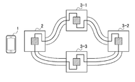
- the information processing system shown in FIG. 1 includes a user terminal 1 used by a user, a basic core 2, and a large number of functional modules 3-1 to 3-n (n is an integer of 1 or more).
- n is an integer of 1 or more.
- the number of user terminals 1 and the basic core 2 is not limited to this. Is fine.
- the number n of the functional modules 3-1 to 3-n connected to the basic core 2 is not particularly limited.
- the user terminal 1 communicates with the basic core 2 by various methods, for example, NFC (registered trademark) (Near Field Communication), Bluetooth (registered trademark), and the like.
- NFC registered trademark
- Bluetooth registered trademark
- functional module 3 when it is not necessary to individually distinguish the functional modules 3-1 to 3-n, these are collectively referred to as “functional module 3”.
- FIG. 1 illustrates a daisy-chain type as an example of a connection mode between the basic core 2 and the functional module 3.
- the basic core 2 serves as one end, one functional module 3-1 is connected to the one end, and the functional module 3-1 is further connected to the functional module 3-1. Further, another function module 3 (not shown) is connected to the function module 3-2.
- the basic core 2 is a hardware device that is used by being connected to one or more functional modules 3, and is paired with the user terminal 1 through short-range wireless communication (for example, communication conforming to the NFC (registered trademark) standard). Do the ring.
- short-range wireless communication for example, communication conforming to the NFC (registered trademark) standard.
- the user terminal 1 is connected to the basic core 2-K and the basic core 2-K by performing pairing with a predetermined basic core 2-K (K is an arbitrary integer value from 1 to m). It recognizes L (L is an arbitrary integer) functional modules 3-K1 to 3-KL. That is, the target connected to the basic core 2-K may be a serial connection of L functional modules 3. The user terminal 1 can recognize these L function modules 3 individually.
- the functional module 3 is a hardware device including, for example, various sensors such as a temperature sensor, operating devices such as push buttons, driving devices such as a motor, and the like.
- the pairing between the user terminal 1 and the basic core 2-K will be described.
- the term “pairing” refers to causing the user terminal 1 to recognize the type, connection state, and the like of the basic core 2-K and the functional modules 3 connected thereto using short-range wireless communication.
- the user terminal 1 recognizes the type of the functional module 3 and the connection status, the H parts corresponding to the connected functional module 3 are displayed on the program creation screen.
- the user terminal 1 is configured by a tablet terminal or the like.
- FIG. 2 is a diagram illustrating an example of a configuration in a state where the basic core and the functional module according to the first embodiment of the present invention are connected.
- FIG. 2 illustrates the basic core 2-E, the function module 3-E1, the function module 3-E2, and the battery unit PP.
- the basic core 2-E includes a battery unit BU, serial ports SP1 and SP2, and a short-range wireless communication unit BT.
- the battery unit BU is, for example, a stabilized DC power supply, and supplies electric power to the basic core 2-E, the function module 3-E1, and the function module 3-E2 with current.
- the serial ports SP1 and SP2 are connection ports (connection connectors) for connecting the basic core 2-E to other hardware or the like.
- the basic core 2-E is provided with serial ports SP1 and SP2, and the functional module 3-E1 is provided with a serial port PS1.
- the basic core 2-E and the function module 3-E1 are connected via the two serial ports SP1 and PS1.
- the function module 3-E1 has a serial port PS2, and the function module 3-E2 has a serial port PS3.
- the function module 3-E1 and the function module 3-E2 have the two serial ports PS2, It is connected via PS3.
- the serial module SP2 of the basic core 2-E may be connected to the functional module 3 located at the end connected in series from the serial port SP1, and a plurality of modules may be connected in a loop via the serial port.
- the short-range wireless communication unit BT includes an IC card or the like for performing short-range wireless communication with other hardware or the like by a method according to a predetermined standard (for example, Bluetooth (registered trademark)).
- the user terminal 1 (not shown in FIG. 2) and the basic core 2-E including the short-range wireless communication unit BT are in short-range by a method according to Bluetooth (registered trademark). Perform wireless communication. Specifically, for example, the execution result (command or the like) of the program created in the user terminal 1 is also transmitted to the basic core 2-E.
- Bluetooth registered trademark
- the basic core 2-E acquires the execution result (command or the like) of the program transmitted from the user terminal 1, and further superimposes the result on the current signal (for power supply) as transmission information. Then, of the function modules 3-E1 and 3-E2, the command is transmitted to the target function module 3 such as a command.
- the function module 3-E1 includes a tire T, and the function module 3-E2 includes a buzzer.
- the functional modules 3-E1 and 3-E2 acquire only the execution result (command or the like) of the program for the own device from the transmission information transmitted from the basic core 2-E.
- the functional module 3-E1 in the example of FIG. 2 drives the tire T according to a command for driving the tire among the execution results (commands and the like) of the program created in the user terminal 1.
- the function module 3-E2 sounds the buzzer according to a command or the like for sounding the buzzer among the execution results (commands and the like) of the program created in the user terminal 1.
- the battery unit PP is connected to the functional module 3-E1.
- the battery unit PP supplies power to the function module 3-E1 as an external power supply, and also supplies power to the function module 3-E2 connected to the function module 3-E1.
- the battery unit PP is not an essential component if the basic core 2 can supply necessary power to the function module 3-E1 and the like.
- the program creation process refers to a process for creating a program for causing one or more function modules 3 connected to the basic core 2 to function.
- a two-wire constant current communication circuit is formed.
- the two-wire constant current communication circuit superimposes a signal current on a power supply constant current, thereby omitting wiring dedicated to communication and connecting only with two wires used for power supply to perform current communication.
- This method has a smaller number of wires compared to a case where a power supply line and a communication line are separately wired, and can reduce the thickness of a cable when the power supply line and the communication line are combined into a single line. Fewer connectors are required.
- the current-type communication method does not complicate the circuit and does not increase the cost and the board size even when stable communication over a long distance is realized. That is, according to this method, an assembly block capable of performing stable data communication with a simple configuration can be realized.
- the two-wire constant current communication circuit has a problem that power supply efficiency is poor.
- the wiring in the connection mode between the basic core 2 and the functional module 3, the wiring does not seem to form a closed loop, but the wiring is folded back at the basic core 2 or the functional module 3 located at the end. For this reason, the configuration is electrically closed loop wiring.
- the functional modules 3 since the functional modules 3 are electrically connected in a row, the current flowing through all the functional modules 3 is the same. For this reason, it is necessary to design a system of the basic core 2 and the functional module 3 according to the functional module 3 (for example, the functional module 3-1) which uses the most current.
- the functional module 3 that does not use the current converts the unused current into heat, and the power supply efficiency deteriorates. Therefore, there is a demand for improving the power supply efficiency, that is, a demand for reducing the power consumption of the functional module 3.
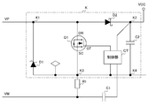
- FIG. 3 is a circuit diagram showing an example of a circuit connected to the two-wire type constant current network shown in FIG. 1, for example, a circuit provided in one predetermined functional module.
- the circuit in FIG. 3 is connected to a two-wire constant current network using a constant current source (not shown) provided in the core module 2.
- 3 is provided in the function module 3.
- the input circuit positive terminal VP and the input circuit negative terminal VM are two-wire connection terminals, and are connected to the constant current source provided in the core module 2.
- the connection is a broad concept including not only a direct connection but also a connection via another element (for example, another function module 3).
- the circuit in FIG. 3 is configured to include a circuit section K having terminals K1 to K4, a current measuring resistor R1, and a capacitor C1.
- the terminal K1 is connected to the input circuit positive terminal VP
- the terminal K3 is connected to one end of the current measuring resistor R1.
- the other end of the current measuring resistor R1 is connected to the input circuit negative terminal VM and one end of the capacitor C1, and the other end of the capacitor C1 is connected to the control unit CT in the circuit unit K.
- a load (not shown) is connected to the terminal K2 of the potential Vcc and the terminal K4.
- the circuit section K has a constant voltage diode D1, a field effect transistor Q1, a Schottky barrier diode D2, a capacitor C2, and a control section CT.
- a constant voltage diode D1, a field effect transistor Q1, a Schottky barrier diode D2, and a series connection of a capacitor C2 are connected in parallel between the terminals K1 and K4.
- An end K2 is provided as a connection end between the Schottky barrier diode D2 and the capacitor C2, and the end K3 and the end K4 are connected at the same potential.
- the control unit CT has an output connected to the gate GT of the field-effect transistor Q1, and an input connected to the terminal K2 of the potential Vcc.
- the control unit CT is also connected to the capacitor C1 as described above and to the terminal K4 (terminal K3).
- the source SC of the field effect transistor Q1 is connected to the terminal K3, and the drain DR of the field effect transistor Q1 is connected to the terminal K1.
- control unit CT switches the state of field effect transistor Q1 as a switching element from one of the ON state and the OFF state to the other according to the value of input potential Vcc. That is, in the circuit of FIG. 3 in a standby state where the load is not operated, when the potential Vcc is higher than the specified voltage, the control unit CT controls the field-effect transistor Q1 to be turned on. As a result, the resistance value between the drain DR and the source SC becomes substantially zero, the circuit K is short-circuited, and the constant-voltage diode D1 does not conduct. Thereby, heat generation from the constant voltage diode D1 is avoided, and the power consumption of the functional module 3 including the circuit of FIG. 3 is greatly reduced.
- the control unit CT controls the field-effect transistor Q1 to be turned off.
- the drain DR and the source SC are substantially insulated from each other, and a constant current is externally supplied to the constant voltage diode D1 to obtain a sufficient voltage required for operating the load. Therefore, the power consumption in this case is equivalent to the conventional case without using the circuit of FIG.
- the power required for the load is sufficiently supplied from the outside in the operating state, while the power consumption is largely suppressed in the standby state.
- the field-effect transistor Q1 has a lower on-resistance, the power-saving effect is exhibited.
- a silicon N-channel MOS field effect transistor can be employed as a specific example of such a field effect transistor for a load switch.
- FIG. 6 is a diagram illustrating an example of a communication waveform when transmitting information for communication from the functional module 3-1 to the core module 2.
- the core module 2, the function module 3-1 and the function module 3-2 form a closed loop and are wired in series.
- the horizontal axis represents time
- the vertical axis represents the voltage between the input circuit positive terminal VP and the input circuit negative terminal VM applied in the functional module 3-1.
- the waveform of the voltage applied in the function module 3-1 is shown in the upper part of FIG. 6 as a communication waveform.
- the horizontal axis indicates time
- the vertical axis indicates the voltage between the input circuit positive terminal VP and the input circuit negative terminal VM applied in the functional module 3-2.
- the function module 3-2 is a function module 3 that does not take any other countermeasures to be described later.
- the function module 3-2 is used.
- the waveform of the voltage applied at -2 is shown in the lower part of FIG.
- the horizontal axes in the upper and lower figures correspond to each time in the upper and lower directions, and the voltages at the same timing can be compared in the upper and lower directions.
- the core module 2, the function module 3-1 and the function module 3-2 are connected in series in a closed loop. Therefore, the actual current between the input circuit positive terminal VP and the input circuit negative terminal VM of each module becomes the same, and the voltage shown in the upper part of FIG. 6 and the voltage shown in the lower part of FIG. The added voltage is applied to the core module 2.
- the information for communication is information composed of a combination of “1” or “0” bits.
- This communication information is transmitted from the functional module 3 to the core module 2 as a pulse waveform signal shown in FIG. 6 having a high-level voltage indicating “0” and a low-level voltage indicating “1”.
- the width of the pulse corresponding to the information for communication is about 50 microseconds.
- the voltage is about 50 microseconds at a low level, about 100 microseconds of one pulse together with about 50 microseconds of the high-level part of an arbitrary length before and after the voltage is about 50 microseconds. It can be said that it is one cycle. That is, the frequency of the communication waveform (pulse waveform) shown in the upper part of FIG. 6 is about 10 KHz.
- the signal of the communication waveform (pulse waveform) shown in the upper part of FIG. the signal of the communication waveform (pulse waveform) shown in the upper part of FIG.
- the switching of the state of the field effect transistor Q1 occurs continuously.
- the switching of the state of the field effect transistor Q1 irrelevant to the communication from the functional module 3 to the core module 2 may occur continuously at a frequency of about 10 KHz as shown in the lower part of FIG.
- the communication waveform (pulse waveform) shown in the upper part of FIG. 6 is superimposed on the voltage waveform between the input circuit positive terminal VP and the input circuit negative terminal VM due to the continuous switching of the state of the field effect transistor Q1. It becomes the same as the voltage waveform in the case.
- the core module 2 which is the transmission destination of the communication information is confused with the pulse wave of the communication information. Easy noise is generated in the function module 3-2.
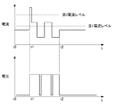
- FIG. 7 is a diagram illustrating an example of a waveform generated as the state of the switch unit is continuously switched by the two-wire constant current communication circuit according to the first embodiment of the present invention.
- the core module 2, the functional module 3-1 and the functional module 3-2 form a closed loop and are wired in series.
- the upper part of FIG. 7 is the same as the upper part of FIG. That is, in the upper part of FIG.
- the horizontal axis indicates time
- the vertical axis indicates the voltage between the input circuit positive terminal VP and the input circuit negative terminal VM applied in the functional module 3-1.
- the waveform of the voltage applied in the functional module 3-1 is shown as the communication waveform in the upper part of FIG.
- the horizontal axis represents time
- the vertical axis represents the voltage between the input circuit positive terminal VP and the input circuit negative terminal VM applied in the functional module 3-2.
- the horizontal axes of the upper and lower figures correspond to the upper and lower times, and the voltages at the same timing can be compared in the upper and lower directions.
- FIG. 6 the horizontal axes of the upper and lower figures correspond to the upper and lower times, and the voltages at the same timing can be compared in the upper and lower directions.
- FIG. 6 the horizontal axes of the upper and lower figures correspond to the upper and lower times, and the voltages at the same timing can be compared in the upper and lower directions.
- FIG. 6 the horizontal axes of the upper and lower
- the core module 2, the function module 3-1 and the function module 3-2 are wired in series in a closed loop. Therefore, similarly to FIG. 6, the actual current between the input circuit positive terminal VP and the input circuit negative terminal VM of each module becomes the same, and the voltage shown in the upper part of FIG. The added voltage is applied to the core module 2.
- the voltage does not continue at the high level during the time when the voltage becomes the high level.
- the high level and the low level are repeated at a high frequency of about 200 KHz, and a pulse having a high voltage with respect to the width on the time axis, that is, a thin pulse is continuously output. It is shown.
- the functional module 3-2 if the voltage between the input circuit positive terminal VP and the input circuit negative terminal VM makes such a change, for example, a low-pass filter that allows only a signal having a frequency of 100 KHz or less to pass is used as the noise removing unit.
- a low-pass filter that allows only a signal having a frequency of 100 KHz or less to pass is used as the noise removing unit.
- the communication waveform (pulse waveform) shown in the upper part of FIG. 7 having a frequency of about 10 KHz passes through the low-pass filter. Therefore, even if the narrow pulse shown in the lower part of FIG. 7 and the communication waveform (pulse waveform) shown in the upper part of FIG. 7 are mixed, only the communication waveform (pulse waveform) shown in the upper part of FIG. 7 can be extracted. .
- the supply of the high-level voltage is divided into a number of narrow pulses shown in the lower part of FIG. These can be cut off with a low-pass filter. This eliminates adverse effects on communication with the core module 2 and improves the reliability of the communication, so that the core module 2 can reliably control the functional module 3 based on the communication.
- the high-level voltage is generated by the control unit CT controlling the field-effect transistor Q1 to be turned off in order to recover the potential Vcc lower than the specified voltage. Therefore, as described above, if the voltage is not maintained at the high level, the time required to recover the potential Vcc will be prolonged.
- the control unit CT may determine the duty ratio for the narrow pulse shown in the lower part of FIG. 7 based on the electric power required to operate the load. That is, if the power required to operate the load is large, it is determined that the time occupied by the high-level voltage in one cycle is lengthened and the time occupied by the low-level voltage is shortened. Conversely, if the power required to operate the load is small, it is determined that the time occupied by the high-level voltage in one cycle is shortened and the time occupied by the low-level voltage is increased. Then, the control unit CT controls the switching of the state of the field-effect transistor Q1 in accordance with the timing at which the determined duty ratio is applied to a frequency of, for example, about 200 KHz.
- the duty ratio is determined to be 0.4 by the control unit CT and applied to the frequency of 200 KHz
- the time occupied by the high-level voltage in 2 microseconds in one cycle is 2 microseconds.
- Seconds, and the time occupied by the low-level voltage is 3 microseconds.
- the supply of the high-level voltage is divided into a large number of narrow pulses shown in the lower part of FIG.
- the second embodiment in which the state of the field effect transistor Q1 is not switched as much as possible may be adopted.
- the system configuration of the second embodiment is the same as the system configuration of the first embodiment of FIG. That is, the information processing system of the second embodiment also includes the user terminal 1 used by the user, the core module 2, and the many function modules 3.
- the configuration of the second embodiment in a state where the core module 2 and the functional module 3 are connected is the same as that of the first embodiment shown in FIG. 2, and the description thereof will be omitted here.
- FIG. 8 is a circuit diagram illustrating a circuit connected to the two-wire constant current communication network according to the second embodiment of the present invention, for example, a circuit provided in one predetermined functional module.
- the circuit of FIG. 8 is connected to a two-wire constant current network using a constant current source (not shown) provided in the core module 2.
- the circuits shown in FIG. 8 are provided in the function modules 3 respectively.
- the input circuit positive terminal VP and the input circuit negative terminal VM are two-wire connection terminals, and are connected to a constant current source provided in the core module 2.
- the circuit in FIG. 8 is configured to include a circuit section L having terminals L1 to L4, a current measuring resistor R1, and a capacitor C1.
- the terminal L1 is connected to the input circuit positive terminal VP
- the terminal L3 is connected to one end of the current measuring resistor R1.
- the other end of the current measuring resistor R1 is connected to the input circuit negative terminal VM and one end of the capacitor C1, and the other end of the capacitor C1 is connected to the negative terminal of the comparator CM1 in the circuit section L, the negative terminal of the comparator CM2, and the current. It is connected to one end of the level comparison resistor R2.
- a load (not shown) is connected to the terminal L2 of the potential Vcc and the terminal L4.
- the circuit unit L includes a constant voltage diode D1, a field effect transistor Q1, a Schottky barrier diode D2, a capacitor C2, a control unit CT, a reference voltage circuit VR, a current level comparison resistor R2, a comparator CM1, , A comparator CM2.
- a constant voltage diode D1, a field effect transistor Q1, a Schottky barrier diode D2 and a capacitor C2 connected in series are connected in parallel.
- An end L2 is provided as a connection end between the Schottky barrier diode D2 and the capacitor C2, and the end L3 and the end L4 are connected at the same potential.
- a reference voltage circuit VR is also connected to the terminal L2.
- the other three terminals of the reference voltage circuit VR are connected to the current level comparison resistor R2, the positive terminal of the comparator CM1, and the positive terminal of the comparator CM2, respectively.
- the output terminal CO1 of the comparator CM1 is connected to the RX terminal of the control unit CT.
- the output terminal CO2 of the comparator CM2 is connected to the INT terminal of the control unit CT.
- the control unit CT has its output from the Drv terminal connected to the gate GT of the field effect transistor Q1, and its input connected to the terminal L2 of the potential Vcc. As described above, the control unit CT has the RX terminal connected to the output terminal CO1 of the comparator CM1, the INT terminal connected to the output terminal CO2 of the comparator CM2, and the terminal L4 (terminal L3).
- the source SC of the field effect transistor Q1 is connected to the terminal L3, and the drain DR of the field effect transistor Q1 is connected to the terminal L1.
- the constant voltage diode D1, the field effect transistor Q1, the Schottky barrier diode D2, and the capacitor C2 are the same as those in the first embodiment, and thus description thereof will be omitted.
- the input of the reference voltage circuit VR is connected to the terminal L2 of the potential Vcc, and the three terminals on the output side are connected to the current level comparison resistor R2, the positive terminal of the comparator CM1, and the positive terminal of the comparator CM2.
- the other end of the current level comparison resistor R2 is connected to the capacitor C1, the negative terminal of the comparator CM1, and the negative terminal of the comparator CM2.
- the comparator CM1 has a positive terminal connected to one end of the current level comparison resistor R2, a negative terminal connected to one end on the input side of the reference voltage circuit VR, the capacitor C1, and a negative terminal of the comparator CM2.
- the terminal CO1 is connected to the RX terminal of the control unit CT.
- the comparator CM2 has a positive terminal connected to the current level comparison resistor R2, a negative terminal connected to one end on the input side of the reference voltage circuit VR, the capacitor C1, and a negative terminal of the comparator CM2, and an output terminal CO2. Are connected to the INT terminal of the control unit CT.
- the reference voltage circuit VR supplies a voltage serving as a reference for comparing current levels to the current level comparison resistor R2 and the comparators CM1 and CM2. That is, the reference voltage circuit VR supplies the comparator CM1 with a reference voltage for comparing the current level with the first threshold value, and generates a voltage generated across the current measuring resistor R1 according to the current level. Allows comparison with
- the first threshold is a threshold for the current level, and is a threshold for obtaining bit information of 1 or 0 from the current.
- the bit information takes a value of 1
- the bit information takes a value of 0.
- the reference voltage circuit VR supplies the comparator CM2 with a reference voltage for comparing the current level with the second threshold value, and generates a voltage generated across the current measuring resistor R1 according to the current level. Allows comparison with That is, the second threshold value is a threshold value for detecting a signal for notifying the start of communication from the current.
- the reference voltage circuit VR outputs 1.5 V to the current level comparison resistor R2 and the reference voltage of the comparator CM1.
- a voltage of 1.6 V is supplied to the positive electrode, and a voltage of 1.7 V is supplied to the positive electrode of the comparator CM2.
- the comparator CM1 compares the level of the current from the capacitor C1 and the first threshold value with the corresponding voltages. If the level of the current from the capacitor C1 exceeds the first threshold value, the comparator CM1 controls the output terminal CO1. A signal of 0 is output to the RX terminal of the unit CT. The signal means a bit value of 0. The comparator CM1 compares the level of the current from the capacitor C1 and the first threshold value with the corresponding voltages, and if the level of the current from the capacitor C1 does not exceed the first threshold value, the output terminal CO1 From the control unit CT to the RX terminal. The signal has a bit value of 1. That is, the comparator CM1 is a comparator for decoding communication information from the current.
- the control unit CT may recognize that the transmission of information has ended, for example, when the state continues for a predetermined time after the input of the signal of 0 to the RX terminal is stopped.
- the comparator CM2 compares the level of the current from the capacitor C1 with the second threshold. If the level of the current from the capacitor C1 exceeds the second threshold, the comparator CM2 connects the output terminal CO2 to the INT terminal of the control unit CT. , 0 signals. This signal means that communication is started.
- the comparator CM2 compares the level of the current from the capacitor C1 with the second threshold value. If the level of the current from the capacitor C1 does not exceed the second threshold value, the comparator CM2 outputs the signal INT of the control unit CT from the output terminal CO2. Output 1 signal to the terminal. This signal has no particular meaning. That is, the comparator CM2 is a comparator for detecting a signal notifying the start of transmission of communication information from the core module 2 to the functional module 3 from the current based on the corresponding voltage.
- the control unit CT changes the state of the field-effect transistor Q1 as a switching element according to the value of the input potential Vcc, the 1 or 0 signal from the comparator CM1, and the 1 or 0 signal from the comparator CM2. Is switched from one of the ON state and the OFF state to the other. That is, as in the first embodiment, in the circuit of FIG. 8 in a standby state in which the load is not operated, when the potential Vcc is higher than the specified voltage, the control unit CT turns on the field effect transistor Q1. To control. As a result, the resistance between the drain DR and the source SC becomes substantially zero, causing the circuit L to be short-circuited, and the constant voltage diode D1 does not conduct. As a result, heat generation from the constant voltage diode D1 is avoided, and the power consumption of the functional module 3 including the circuit of FIG. 8 is greatly reduced.
- the control unit CT turns off the field effect transistor Q1.
- the drain DR and the source SC are substantially insulated from each other, and a constant current is externally supplied to the constant voltage diode D1 to obtain a sufficient voltage required for operating the load. Therefore, the power consumption in this case is equivalent to the conventional case without using the circuit of FIG.
- control unit CT recognizes at least a part of the communication information transmitted from the core module 2 based on the signal of 1 or 0 from the comparator CM1.
- the control unit CT may be able to recognize, from the communication information, information that can specify the functional module 3 that is the destination, information on the bit length of the communication information, and the like. Thereby, the control unit CT can recognize whether the information for communication has been transmitted to the function module 3. Further, thereby, the control unit CT can recognize that the communication has been completed when the transmission of the communication information for the bit length is performed.
- the bit length of the communication information may be a fixed length. In this case, even if the information of the bit length of the communication information is not included, it is possible to recognize that the communication has been completed when the transmission of the fixed length is performed.
- the sleep state means that the control by the control unit CT to restore the potential Vcc to the specified voltage is made to sleep (sleep) until communication from the core module 2 to the self-function module 3 or another function module 3 is started.
- This is a state in which the switching between the ON state and the OFF state of the field effect transistor Q1 does not occur. That is, even when the functional module 3 is in the standby state in which the load is not operated, the potential Vcc gradually decreases, and when the functional module 3 reaches a state lower than the specified voltage, in the circuit of FIG. Q1 was controlled to be turned off.
- the control unit CT controls the field-effect transistor Q1 to repeat the ON state and the OFF state, and each time, the communication waveform (pulse) shown in FIG. A waveform similar to (waveform) is generated, which causes a malfunction.
- the control unit CT does not immediately turn off the field-effect transistor Q1 and switches the field effect transistor Q1 from the core module 2 to the self-function module 3 or another function module 3. Even if the power supply is turned off after the communication starts, the power supply to the load can be completed in time, so that the function module 3 is sufficient.
- control by the control unit CT to restore the potential Vcc to the specified voltage is set to sleep (sleep) until communication from the core module 2 to the self-function module 3 or another function module 3 is started, and the electric field effect during the sleep is performed. It is conceivable that the switching of the transistor Q1 between the on state and the off state does not occur. Further, until the communication between the core module 2 and the self-function module 3 or another function module 3 ends, the field-effect transistor Q1 remains in the off state, and after the communication ends, switching to the on state is performed. It is possible to make it possible.
- the control unit CT switches the field-effect transistor Q1 from the on-state to the off-state when the comparator module CM2 detects a signal notifying the start of transmission of communication information from the core module 2 in the functional module 3, It is possible to switch. Therefore, in this case, when the information for communication is transmitted from another functional module 3 to the core module 2, the amount of the voltage change due to the switching of the state of the field effect transistor Q 1, which becomes a noise, is determined by the circuit of FIG. Is equivalent to Further, the control unit CT, when recognizing that the transmission of the information to another functional module 3 has been completed or recognizing that the detection of the transmission of the information by the comparator CM1 has been completed, in the functional module 3, causes the field effect transistor Q1 to operate.
- the control unit CT causes the control by the control unit CT to restore the potential Vcc to the specified voltage, until the communication from the core module 2 to the own function module 3 or another function module 3 is started (sleeps). . Further, until the communication between the core module 2 and the self-function module 3 or another function module 3 ends, the switching of the state of the field-effect transistor Q1 is limited to be kept off, and after the communication ends. , Enabling switching to the on state. In this way, when communication information is transmitted from another functional module 3 to the core module 2, the occurrence of a voltage change due to the switching of the state of the field effect transistor Q1, which is a noise, is avoided during communication. You. This eliminates adverse effects on the communication to the core module 2 and improves the reliability of the communication, so that the core module 2 reliably controls another functional module 3 including the circuit of FIG. 8 based on the communication. Can be done.
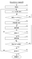
- FIG. 9 is a flowchart illustrating a flow of a low power consumption mode control process performed by the two-wire constant current communication circuit according to the second embodiment of the present invention.
- the control unit CT performs an initialization process.
- the initialization process is, for example, a process of initial recognition of each core module 2 and many function modules 3 necessary for communication between the core module 2 and many function modules 3.
- the control unit CT shifts to a sleep state. That is, the control by the control unit CT to restore the potential Vcc to the specified voltage is made to sleep.
- the control unit CT determines whether the level of the current flowing between the input circuit positive terminal VP and the input circuit negative terminal VM is equal to or higher than the second threshold.
- step S3 If the level of the current flowing between the input circuit positive terminal VP and the input circuit negative terminal VM is less than the second threshold, it is determined as NO in step S3, and the determination processing of step S3 is repeated. If a current equal to or more than the second threshold value is detected while the determination process of step S3 is repeated, it is determined that the answer is YES in the next step S3, and the process proceeds to step S4.
- step S4 the control unit CT stops the sleep state and shifts to a state of activating the recovery of the potential Vcc to the specified voltage. Thereby, the communication process by the control unit CT can be executed.
- step S5 the control unit CT performs a communication process.
- step S5 the control unit CT reads a signal from the comparator CM1 and extracts at least a destination of information. Note that the length of the communication may be extracted.
- step S6 the control unit CT determines whether the destination of the information is the self-function module 3. If the destination of the information is different from the own module, it is determined as NO in step S6, and the process proceeds to step S8.
- step S6 if the destination of the information is the own module, it is determined to be YES, and the process proceeds to step S7.
- step S7 the control unit CT activates the load based on the result of the communication processing in step S5, that is, based on the control of the core module 2.
- step S8 the control unit CT determines whether the communication from the core module 2 to the own function module 3 or another function module 3 has been completed. If the communication is in progress, NO is determined in step S8, and the process returns to the communication process of step S5, and the subsequent processes are repeated. In step S8, if the communication ends, the control unit CT determines that the answer is YES, and the process proceeds to step S9. In step S9, the control unit CT determines whether an instruction to end the low power consumption mode control process has been issued.
- the processing termination instruction is not particularly limited, but in the present embodiment, the processing termination instruction from the core module 2 is employed.
- step S9 unless an instruction to end the process is issued from the core module 2, it is determined as NO in step S9, the process returns to step S2, and the subsequent processes are repeated. On the other hand, when an instruction to end the process is issued from the core module 2, YES is determined in step S9, and the low power consumption mode control process ends.
- FIG. 10 is a diagram illustrating an example of a waveform obtained by the two-wire constant current communication circuit according to the second embodiment of the present invention.
- the horizontal axis indicates time
- the vertical axis indicates the current between the input circuit positive terminal VP and the input circuit negative terminal VM.
- the horizontal axis represents time
- the vertical axis represents the voltage between the input circuit positive terminal VP and the input circuit negative terminal VM.
- FIG. 10 shows a waveform of a voltage applied to the functional module 3 when information for communication is transmitted from the functional module 3 to the core module 2.
- the horizontal axes of the upper and lower figures are assumed to correspond to the respective times in the upper and lower directions, and the current and the voltage at the same timing can be compared in the upper and lower directions.
- a pulse current having a level exceeding the second current level (second threshold) is transmitted from the core module 2 as a signal notifying the start of transmission of communication information.
- second threshold the second current level
- the control unit CT performs a communication process.
- a pulse current having a level exceeding the first current level (first threshold) is intermittently transmitted from the core module 2 as bit information indicating “0” in the communication information.
- the comparator CM1 extracts the pulse current having a level exceeding the first threshold as information of 0 and the pulse current having a level not exceeding the first threshold as 1 as information.
- the control unit CT has recognized that the destination of the information for communication from the core module 2 was the self-function module 3. That is, it is determined to be YES at the timing when step S6 in FIG. 9 is executed, and the process proceeds to step S7.
- the control unit CT transmits the information for communication to the core module 2 and activates the load according to the information for communication from the core module 2.
- a voltage is applied between the input circuit positive terminal VP and the input circuit negative terminal VM.
- step S8 in FIG. 10 determines whether the communication has ended. It is assumed that the communication is continued until time t2, and at the timing when step S8 in FIG. 9 is executed, it is determined to be NO, and the process returns to the communication process of step S5, and the subsequent processes are repeated. Each of the above processes is repeated until time t2.
- step S8 in FIG. 9 communication with the core module 2 ends, and in step S8 in FIG. 9, it is determined to be YES, and the process proceeds to step S9 in FIG.
- step S9 in FIG. 9 the control unit CT determines that there is no instruction to end the low power consumption mode control process, and the process returns to step S2 in FIG. 9. Is repeated.
- the present invention is not limited to the above-described embodiment, and modifications, improvements, and the like within a range that can achieve the object of the present invention are included in the present invention. is there.
- a battery capable of supplying a stable direct current may be employed, and the supplied current is not limited to direct current, and an alternating current may be supplied by employing various means such as an inverter. .
- the electronic device according to the present invention may be provided with power line communication. In this way, power supply and communication can be performed using only two lines. In addition, this makes it possible to form a simple circuit that is strong against noise. That is, the present invention can be applied to an electronic device that can stabilize data communication with a simple configuration.
- the field effect transistor Q1 included in the electronic device according to the present invention may also serve as a switching element provided for power line communication. By doing so, it is possible to reduce the number of components of the power circuit.
- the components for measuring the power supply voltage that constitute the electronic device according to the present invention may also be the components built in the microcomputer provided for the power line communication. By doing so, it is not necessary to separately add a comparator, and the number of components can be reduced.
- the field-effect transistor Q1 is employed.
- any device having a switching function is sufficient, and the present invention is not particularly limited to this.
- the functional module 3 it suffices to provide an element for changing the resistance value. This is because if the resistance value can be changed and the voltage between both ends of the functional module 3 can be suppressed, the power of the functional module 3 can be suppressed.
- the present invention is not limited to this, and a power supply line and a communication line may be separately provided.
- the connection is not limited to the wired connection only, and wireless power supply and communication may be combined.
- the numbers of the basic cores 2 and the functional modules 3 are not particularly limited to the above-described embodiments. That is, the number of the basic cores 2 and the number of the function modules 3 may be the same or different. That is, one functional module 3 may be connected to one basic core 2.
- FIG. 4 illustrates a star type as an example of a connection mode between the basic core 2 and the functional module 3.
- the star type shown in FIG. 4 is a connection mode in which the basic core 2 and two or more functional modules 3 (three functional modules 3-1 to 3-3 in the example of FIG. 4) are connected in a star type. .
- FIG. 5 illustrates a loop type as an example of a connection mode between the basic core 2 and the functional module 3.
- the basic core 2 and one or more functional modules 3 form a loop in a predetermined order (in the example of FIG. 5, the order of the basic core 2 and the functional modules 3-1 to 3-3). Are connected to form a closed loop.
- connection mode is basically the above connection mode. However, if a configuration that electrically forms a closed loop wiring is adopted, an arbitrary connection mode can be adopted by combining the above connection modes.
- a signal transmitted from the basic core 2 to supply power to one or more functional modules 3 is only required to be in a form capable of transmitting power by a current method. You may.
- the two-wire constant current communication network is provided in the set of the core module 2 and the functional module 3.
- the two-wire constant current communication network is not limited to this.
- a two-wire constant current communication network may be used in an arbitrary set made up of a module having a constant current source (master) and another module (slave). May be provided.
- the information for communication is a signal having a high-level voltage indicating “0” and a low-level voltage indicating “1” as a pulse waveform signal illustrated in FIG. Is transmitted to the core module 2 by way of example, but this is an example, and the present invention is not limited to this. That is, the information of 0 or 1 may be a reverse combination of the high-level voltage and the low-level voltage, where the low-level voltage indicates “0” and the high-level voltage indicates “1”. You can show.
- the comparator CM1 extracts the pulse current of the level exceeding the first threshold as information of 1 and the pulse current of the level not exceeding the first threshold as 0, but extracts this as an example. But it is not limited to this. That is, the extracted information of 0 or 1 may be a reverse combination of whether or not the pulse current exceeds the first threshold, and the pulse current that does not exceed the first threshold is the information of the pulse current exceeding the first threshold as 0. The current may be extracted as one.
- the second current level (second threshold) is a current level (threshold) higher than the first current level (first threshold). I can't. That is, the second current level (second threshold) may be the same current level (threshold) as the first current level (first threshold).
- the time during which the high-level voltage is obtained is controlled so that the state of the field-effect transistor Q1 is continuously switched at a high frequency.
- this is an example, and the present invention is not limited to this. Absent.
- the state of the field effect transistor Q1 may be controlled so as to be continuously switched at a high frequency as a configuration in which the time when the voltage at the low level becomes the voltage including the current measuring resistor R1 can be shortcutted.
- the above-described series of processing can be executed by hardware or can be executed by software. That is, it is sufficient that the information processing system has a function capable of executing the above-described series of processing as a whole.
- one functional block may be constituted by hardware alone, may be constituted by software alone, or may be constituted by a combination thereof.
- a program constituting the software is installed in a computer or the like from a network or a recording medium.
- the computer may be a computer embedded in dedicated hardware.
- the computer may be a computer that can execute various functions by installing various programs, for example, a general-purpose smartphone or a personal computer other than a server.
- a recording medium including such a program is not only constituted by a removable medium (not shown) distributed separately from the apparatus main body in order to provide the user with the program, but also a state in which the recording medium is pre-installed in the apparatus main body. And a recording medium provided to the user.
- steps for describing a program recorded on a recording medium are not limited to processing performed in chronological order according to the order, but are not necessarily performed in chronological order, but are performed in parallel or individually. This includes the processing to be executed. Also, in this specification, the term system refers to an entire device including a plurality of devices and a plurality of means.
- the electronic device to which the present invention is applied can take various embodiments having the following configurations. That is, the electronic device to which the present invention is applied (for example, the functional module 3 in FIG. 1) In an electronic device including at least a part of a constant current network connected to a predetermined load, A control unit that controls an applied voltage to the predetermined load based on a state related to the predetermined load (for example, a control unit CT in FIG. 3) An electronic device having the above is sufficient.
- the electronic device includes: A path where at least a part of the voltage applied to the predetermined load is generated when a constant current flows through the constant current network (for example, a path from terminal K1 to terminal K3 via constant voltage diode D1 in FIG. 3).
- a switch unit for example, the field-effect transistor Q1 in FIG. 3 for switching between short-circuiting of the path and cancellation of short-circuiting of the path;
- the control unit controls a voltage applied to the predetermined load by switching a state of the switch unit.
- the electronic device includes: A module (eg, the functional module 3 of FIG. 1) having the predetermined load and the electronic device is included in the constant current network (eg, the circuit K of FIG. 3);
- the constant current network when information for communication is transmitted as a first pulse which repeats a voltage level at a first frequency,
- the control unit for example, the control unit CT in FIG. 3
- the state of the switch unit for example, the field effect transistor Q1 in FIG. 3
- the predetermined load is changed in the form of a second pulse that repeats a voltage level at the second frequency. Is controlled.
- the control unit executes control for determining a duty ratio in the second pulse based on power required for the predetermined load. By doing so, it is possible to supply electric power according to the electric power required for operating the load.
- the electronic device includes: A module having the predetermined load and the electronic device (for example, the functional module 3 of FIG. 1) is included in the constant current network;
- a first detection unit for example, a comparator CM2 in FIG. 8) that detects the start of transmission of the information in the module;
- the control unit for example, the control unit CT in FIG. 8) In the module, When the start of transmission of the information is detected by the first detection unit, The state of the switch unit (for example, the field effect transistor Q1 in FIG. 8) From the short-circuit state of the path, to the release state of the short-circuit of the path, Switch.
- the first detection unit is, for example, the comparator CM2 in FIG. 8, but this is an example, and is not limited to the comparator. That is, any one that can detect the start of transmission of the information for communication transmitted in the constant current network in the module can be adopted. For example, a combination of an A / D converter and a program determiner may be used.
- the electronic device includes: The control unit (for example, the control unit CT in FIG. 8) In the module (for example, the functional module 3 in FIG. 1), When recognizing the end of the transmission of the information, The state of the switch unit (for example, the field effect transistor Q1 in FIG. 8) From the state of release of the short-circuit of the path, to the state of short-circuit of the path, Switch. By doing so, the state of the field effect transistor Q1 is switched after the communication is completed, so that the adverse effect on the communication from the self-function module 3 or another function module 3 to the core module 2 is eliminated. be able to.
- the control unit for example, the control unit CT in FIG. 8
- the state of the switch unit for example, the field effect transistor Q1 in FIG. 8 From the state of release of the short-circuit of the path, to the state of short-circuit of the path, Switch. By doing so, the state of the field effect transistor Q1 is switched after the communication is completed, so that the adverse effect on the communication from the self-function module
- the electronic device includes: A second detection unit that detects the end of transmission of the information in the module,
- the control unit for example, the control unit CT in FIG. 8) In the module (for example, the functional module 3 in FIG. 1),
- the second detection unit for example, the comparator CM1 in FIG. 8
- the state of the switch unit for example, the field effect transistor Q1 in FIG. 3 From the state of release of the short-circuit of the path, to the state of short-circuit of the path, Switch.
- the second detection unit is, for example, the comparator CM1 in FIG. 8, but this is an example, and is not limited to the comparator.
- any one that can detect the end of the transmission of the information for communication transmitted in the constant current network in the module can be adopted.
- a combination of an A / D converter and a program determiner may be used.
- the first detection unit for example, the comparator CM2 in FIG. 8
- the second detection unit may serve as the second detection unit.
- it is not necessary to separately provide a second detection unit for example, the comparator CM1 in FIG. 8.
- the state of the field effect transistor Q1 is switched after the communication is completed, so that the adverse effect on the communication from the self-function module 3 or another function module 3 to the core module 2 is eliminated. be able to.
- the electronic device includes: The control unit (for example, the control unit CT in FIG. 8) In the module (for example, the functional module 3 in FIG. 1), Until the end of transmission of the information is recognized, The state of the switch unit (for example, the field effect transistor Q1 in FIG. 8) Without switching in the state of the release of the short-circuit of the route, When recognizing the end of the transmission of the information, The state of the switch unit (for example, the field effect transistor Q1 in FIG. 8) From the state of release of the short-circuit of the path, to the state of short-circuit of the path, Switch. By doing so, the state of the field effect transistor Q1 is switched after the communication is completed, so that the adverse effect on the communication from the self-function module 3 or another function module 3 to the core module 2 is eliminated. be able to.
- the control unit for example, the control unit CT in FIG. 8
- the state of the switch unit for example, the field effect transistor Q1 in FIG. 8
- the state of the switch unit for example, the field
- the electronic device includes: A second detection unit that detects the end of transmission of the information in the module,
- the control unit for example, the control unit CT in FIG. 8) In the module (for example, the functional module 3 in FIG. 1), Until the end of the transmission of the information is detected by the second detection unit (for example, the comparator CM1 in FIG. 8).
- the state of the switch unit for example, the field effect transistor Q1 in FIG. 8) Without switching in the state of the release of the short-circuit of the route,
- the second detection unit for example, the comparator CM1 in FIG. 8
- the state of the switch unit for example, the field effect transistor Q1 in FIG.
- the second detection unit is, for example, the comparator CM1 in FIG. 8, but this is an example, and is not limited to the comparator. That is, any one that can detect the end of the transmission of the information for communication transmitted in the constant current network in the module can be adopted. For example, a combination of an A / D converter and a program determiner may be used.
- the first detection unit for example, the comparator CM2 in FIG. 8
- the second detection unit may serve as the second detection unit. In this case, it is not necessary to separately provide a second detection unit (for example, the comparator CM1 in FIG. 8). By doing so, the state of the field effect transistor Q1 is switched after the communication is completed, so that the adverse effect on the communication from the self-function module 3 or another function module 3 to the core module 2 is eliminated. be able to.
Abstract
Priority Applications (6)
| Application Number | Priority Date | Filing Date | Title |
|---|---|---|---|
| US17/254,588 US11205960B2 (en) | 2018-06-20 | 2019-06-18 | Electronic device with a module using power line communication |
| SG11202012626YA SG11202012626YA (en) | 2018-06-20 | 2019-06-18 | Electronic device |
| JP2020519152A JP6793879B2 (ja) | 2018-06-20 | 2019-06-18 | 電子機器 |
| EP19823437.9A EP3806341B1 (fr) | 2018-06-20 | 2019-06-18 | Dispositif électronique |
| CN201980040685.3A CN112313883B (zh) | 2018-06-20 | 2019-06-18 | 电子设备 |
| KR1020217000620A KR102328549B1 (ko) | 2018-06-20 | 2019-06-18 | 전자 기기 |
Applications Claiming Priority (2)
| Application Number | Priority Date | Filing Date | Title |
|---|---|---|---|
| JP2018117366 | 2018-06-20 | ||
| JP2018-117366 | 2018-06-20 |
Publications (1)
| Publication Number | Publication Date |
|---|---|
| WO2019244886A1 true WO2019244886A1 (fr) | 2019-12-26 |
Family
ID=68983854
Family Applications (1)
| Application Number | Title | Priority Date | Filing Date |
|---|---|---|---|
| PCT/JP2019/024092 WO2019244886A1 (fr) | 2018-06-20 | 2019-06-18 | Dispositif électronique |
Country Status (8)
| Country | Link |
|---|---|
| US (1) | US11205960B2 (fr) |
| EP (1) | EP3806341B1 (fr) |
| JP (1) | JP6793879B2 (fr) |
| KR (1) | KR102328549B1 (fr) |
| CN (1) | CN112313883B (fr) |
| SG (1) | SG11202012626YA (fr) |
| TW (1) | TW202019065A (fr) |
| WO (1) | WO2019244886A1 (fr) |
Cited By (1)
| Publication number | Priority date | Publication date | Assignee | Title |
|---|---|---|---|---|
| WO2022111296A1 (fr) * | 2020-11-30 | 2022-06-02 | Qingdao Haier Air Conditioner General Corp., Ltd. | Circuit d'alimentation pour véhicule de loisirs |
Citations (6)
| Publication number | Priority date | Publication date | Assignee | Title |
|---|---|---|---|---|
| WO1999048340A1 (fr) * | 1998-03-13 | 1999-09-23 | And Software Limited | Traitement de liquides |
| JP2003163090A (ja) | 2001-11-26 | 2003-06-06 | Matsushita Electric Works Ltd | 照明装置 |
| JP4648195B2 (ja) * | 2003-10-21 | 2011-03-09 | パナソニック株式会社 | 設備機器用通信回路 |
| JP2012069505A (ja) * | 2010-08-25 | 2012-04-05 | Panasonic Corp | 照明光通信装置 |
| JP2014135716A (ja) * | 2012-12-11 | 2014-07-24 | Panasonic Corp | 可視光通信装置 |
| JP2017156827A (ja) | 2016-02-29 | 2017-09-07 | ブラザー工業株式会社 | 印刷システム |
Family Cites Families (12)
| Publication number | Priority date | Publication date | Assignee | Title |
|---|---|---|---|---|
| US6278728B1 (en) | 1998-03-18 | 2001-08-21 | Cisco Technology, Inc. | Remote XDSL transceiver unit and method of operation |
| JP2004153983A (ja) * | 2002-11-01 | 2004-05-27 | Sharp Corp | スイッチング電源装置 |
| KR100727354B1 (ko) * | 2005-11-09 | 2007-06-13 | 주식회사 유양정보통신 | 발광 다이오드 정전류 펄스폭 변조 구동 회로 |
| US9161406B2 (en) * | 2011-01-10 | 2015-10-13 | Eldolab Holding B.V. | LED driver and lighting application for wattage control |
| JP5785814B2 (ja) * | 2011-08-18 | 2015-09-30 | ローム株式会社 | スイッチング電源の制御回路、制御方法ならびにそれを用いたスイッチング電源および電子機器 |
| WO2013090945A1 (fr) * | 2011-12-16 | 2013-06-20 | Advanced Lighting Technologies, Inc. | Procédé et système de modernisation par lampes à diodes électroluminescentes, à longue durée de vie, bon marché, et à facteur de puissance proche de l'unité |
| EP2883420B1 (fr) * | 2012-08-07 | 2020-06-24 | Signify Holding B.V. | Dispositif d'alimentation électrique |
| JP5502216B1 (ja) * | 2013-02-28 | 2014-05-28 | 三菱電機株式会社 | 電気負荷の分岐給電制御装置及び分岐給電制御方法 |
| US9374855B2 (en) * | 2013-10-24 | 2016-06-21 | Osram Sylvania Inc. | Power line communication for lighting systems |
| US9385598B2 (en) * | 2014-06-12 | 2016-07-05 | Koninklijke Philips N.V. | Boost converter stage switch controller |
| JP6555612B2 (ja) * | 2015-07-03 | 2019-08-07 | パナソニックIpマネジメント株式会社 | 調光装置 |
| JP6748038B2 (ja) | 2017-08-15 | 2020-08-26 | Vivita株式会社 | 情報処理装置 |
-
2019
- 2019-06-18 JP JP2020519152A patent/JP6793879B2/ja active Active
- 2019-06-18 SG SG11202012626YA patent/SG11202012626YA/en unknown
- 2019-06-18 KR KR1020217000620A patent/KR102328549B1/ko active IP Right Grant
- 2019-06-18 EP EP19823437.9A patent/EP3806341B1/fr active Active
- 2019-06-18 CN CN201980040685.3A patent/CN112313883B/zh active Active
- 2019-06-18 WO PCT/JP2019/024092 patent/WO2019244886A1/fr unknown
- 2019-06-18 US US17/254,588 patent/US11205960B2/en active Active
- 2019-06-19 TW TW108121191A patent/TW202019065A/zh unknown
Patent Citations (6)
| Publication number | Priority date | Publication date | Assignee | Title |
|---|---|---|---|---|
| WO1999048340A1 (fr) * | 1998-03-13 | 1999-09-23 | And Software Limited | Traitement de liquides |
| JP2003163090A (ja) | 2001-11-26 | 2003-06-06 | Matsushita Electric Works Ltd | 照明装置 |
| JP4648195B2 (ja) * | 2003-10-21 | 2011-03-09 | パナソニック株式会社 | 設備機器用通信回路 |
| JP2012069505A (ja) * | 2010-08-25 | 2012-04-05 | Panasonic Corp | 照明光通信装置 |
| JP2014135716A (ja) * | 2012-12-11 | 2014-07-24 | Panasonic Corp | 可視光通信装置 |
| JP2017156827A (ja) | 2016-02-29 | 2017-09-07 | ブラザー工業株式会社 | 印刷システム |
Non-Patent Citations (1)
| Title |
|---|
| See also references of EP3806341A4 |
Cited By (2)
| Publication number | Priority date | Publication date | Assignee | Title |
|---|---|---|---|---|
| WO2022111296A1 (fr) * | 2020-11-30 | 2022-06-02 | Qingdao Haier Air Conditioner General Corp., Ltd. | Circuit d'alimentation pour véhicule de loisirs |
| CN115053425A (zh) * | 2020-11-30 | 2022-09-13 | 青岛海尔空调器有限总公司 | 休闲车的电力电路 |
Also Published As
| Publication number | Publication date |
|---|---|
| SG11202012626YA (en) | 2021-02-25 |
| CN112313883B (zh) | 2022-03-01 |
| CN112313883A (zh) | 2021-02-02 |
| EP3806341A4 (fr) | 2021-08-11 |
| US11205960B2 (en) | 2021-12-21 |
| KR20210008916A (ko) | 2021-01-25 |
| US20210194361A1 (en) | 2021-06-24 |
| KR102328549B1 (ko) | 2021-11-17 |
| JPWO2019244886A1 (ja) | 2020-07-16 |
| EP3806341A1 (fr) | 2021-04-14 |
| EP3806341B1 (fr) | 2022-10-12 |
| JP6793879B2 (ja) | 2020-12-02 |
| TW202019065A (zh) | 2020-05-16 |
Similar Documents
| Publication | Publication Date | Title |
|---|---|---|
| KR102070713B1 (ko) | 액티브/IEEE 표준 기반의 PoE(Power over Ethernet) 낮은 대기 전력 회로 아키텍처 | |
| EP3603343B1 (fr) | Circuit de commande de del double | |
| US20130024046A1 (en) | Power transmission controller, power reception controller, power transmission system, and data communication method of power transmission system | |
| JP2006134338A (ja) | コンピュータおよびその制御方法{computerandcontrolmethodthereof} | |
| JP2015173031A (ja) | 光源駆動装置および光源駆動方法 | |
| WO2019244886A1 (fr) | Dispositif électronique | |
| AU2013275161B2 (en) | Closed-circuit power line communication system for large capacity load | |
| US9088473B2 (en) | Data communication system, data carrier driving apparatus, and data carrier apparatus | |
| US9219413B2 (en) | Power supplies responsive to multiple control signal formats | |
| US9145100B2 (en) | In-vehicle ECU | |
| CN104717092B (zh) | 具有待机运行的主从通信系统 | |
| JP7081443B2 (ja) | 信号処理装置、および情報書換装置 | |
| TWI648952B (zh) | 利用信號線分時傳輸信號和電能的複用電路系統 | |
| US20220294275A1 (en) | Efficient wireless power design | |
| CN213534621U (zh) | 一种电车触摸式启动电路及电车 | |
| CN106849619B (zh) | 电路装置、电子设备以及谐振电路的驱动方法 | |
| JP2007110354A (ja) | 画像形成装置 | |
| JP3906769B2 (ja) | 通信装置 | |
| JP2003110470A (ja) | 2線式データ通信装置 | |
| JP2017055624A (ja) | 回路装置及び電子機器 | |
| JP2014123312A (ja) | Usbコントローラおよびその制御方法 | |
| JP2011103710A (ja) | 電気負荷制御装置 |
Legal Events
| Date | Code | Title | Description |
|---|---|---|---|
| 121 | Ep: the epo has been informed by wipo that ep was designated in this application |
Ref document number: 19823437 Country of ref document: EP Kind code of ref document: A1 |
|
| ENP | Entry into the national phase |
Ref document number: 2020519152 Country of ref document: JP Kind code of ref document: A |
|
| NENP | Non-entry into the national phase |
Ref country code: DE |
|
| ENP | Entry into the national phase |
Ref document number: 20217000620 Country of ref document: KR Kind code of ref document: A |
|
| ENP | Entry into the national phase |
Ref document number: 2019823437 Country of ref document: EP Effective date: 20210108 |