WO2019235560A1 - フィラー含有フィルム - Google Patents
フィラー含有フィルム Download PDFInfo
- Publication number
- WO2019235560A1 WO2019235560A1 PCT/JP2019/022492 JP2019022492W WO2019235560A1 WO 2019235560 A1 WO2019235560 A1 WO 2019235560A1 JP 2019022492 W JP2019022492 W JP 2019022492W WO 2019235560 A1 WO2019235560 A1 WO 2019235560A1
- Authority
- WO
- WIPO (PCT)
- Prior art keywords
- filler
- resin layer
- insulating resin
- containing film
- film
- Prior art date
- Legal status (The legal status is an assumption and is not a legal conclusion. Google has not performed a legal analysis and makes no representation as to the accuracy of the status listed.)
- Ceased
Links
Images


Classifications
-
- C—CHEMISTRY; METALLURGY
- C09—DYES; PAINTS; POLISHES; NATURAL RESINS; ADHESIVES; COMPOSITIONS NOT OTHERWISE PROVIDED FOR; APPLICATIONS OF MATERIALS NOT OTHERWISE PROVIDED FOR
- C09J—ADHESIVES; NON-MECHANICAL ASPECTS OF ADHESIVE PROCESSES IN GENERAL; ADHESIVE PROCESSES NOT PROVIDED FOR ELSEWHERE; USE OF MATERIALS AS ADHESIVES
- C09J7/00—Adhesives in the form of films or foils
- C09J7/30—Adhesives in the form of films or foils characterised by the adhesive composition
- C09J7/35—Heat-activated
-
- C—CHEMISTRY; METALLURGY
- C09—DYES; PAINTS; POLISHES; NATURAL RESINS; ADHESIVES; COMPOSITIONS NOT OTHERWISE PROVIDED FOR; APPLICATIONS OF MATERIALS NOT OTHERWISE PROVIDED FOR
- C09J—ADHESIVES; NON-MECHANICAL ASPECTS OF ADHESIVE PROCESSES IN GENERAL; ADHESIVE PROCESSES NOT PROVIDED FOR ELSEWHERE; USE OF MATERIALS AS ADHESIVES
- C09J171/00—Adhesives based on polyethers obtained by reactions forming an ether link in the main chain; Adhesives based on derivatives of such polymers
- C09J171/08—Polyethers derived from hydroxy compounds or from their metallic derivatives
- C09J171/10—Polyethers derived from hydroxy compounds or from their metallic derivatives from phenols
- C09J171/12—Polyphenylene oxides
-
- C—CHEMISTRY; METALLURGY
- C08—ORGANIC MACROMOLECULAR COMPOUNDS; THEIR PREPARATION OR CHEMICAL WORKING-UP; COMPOSITIONS BASED THEREON
- C08K—Use of inorganic or non-macromolecular organic substances as compounding ingredients
- C08K3/00—Use of inorganic substances as compounding ingredients
- C08K3/01—Use of inorganic substances as compounding ingredients characterized by their specific function
- C08K3/013—Fillers, pigments or reinforcing additives
-
- C—CHEMISTRY; METALLURGY
- C09—DYES; PAINTS; POLISHES; NATURAL RESINS; ADHESIVES; COMPOSITIONS NOT OTHERWISE PROVIDED FOR; APPLICATIONS OF MATERIALS NOT OTHERWISE PROVIDED FOR
- C09J—ADHESIVES; NON-MECHANICAL ASPECTS OF ADHESIVE PROCESSES IN GENERAL; ADHESIVE PROCESSES NOT PROVIDED FOR ELSEWHERE; USE OF MATERIALS AS ADHESIVES
- C09J11/00—Features of adhesives not provided for in group C09J9/00, e.g. additives
- C09J11/02—Non-macromolecular additives
- C09J11/04—Non-macromolecular additives inorganic
-
- C—CHEMISTRY; METALLURGY
- C09—DYES; PAINTS; POLISHES; NATURAL RESINS; ADHESIVES; COMPOSITIONS NOT OTHERWISE PROVIDED FOR; APPLICATIONS OF MATERIALS NOT OTHERWISE PROVIDED FOR
- C09J—ADHESIVES; NON-MECHANICAL ASPECTS OF ADHESIVE PROCESSES IN GENERAL; ADHESIVE PROCESSES NOT PROVIDED FOR ELSEWHERE; USE OF MATERIALS AS ADHESIVES
- C09J163/00—Adhesives based on epoxy resins; Adhesives based on derivatives of epoxy resins
-
- C—CHEMISTRY; METALLURGY
- C09—DYES; PAINTS; POLISHES; NATURAL RESINS; ADHESIVES; COMPOSITIONS NOT OTHERWISE PROVIDED FOR; APPLICATIONS OF MATERIALS NOT OTHERWISE PROVIDED FOR
- C09J—ADHESIVES; NON-MECHANICAL ASPECTS OF ADHESIVE PROCESSES IN GENERAL; ADHESIVE PROCESSES NOT PROVIDED FOR ELSEWHERE; USE OF MATERIALS AS ADHESIVES
- C09J201/00—Adhesives based on unspecified macromolecular compounds
-
- C—CHEMISTRY; METALLURGY
- C09—DYES; PAINTS; POLISHES; NATURAL RESINS; ADHESIVES; COMPOSITIONS NOT OTHERWISE PROVIDED FOR; APPLICATIONS OF MATERIALS NOT OTHERWISE PROVIDED FOR
- C09J—ADHESIVES; NON-MECHANICAL ASPECTS OF ADHESIVE PROCESSES IN GENERAL; ADHESIVE PROCESSES NOT PROVIDED FOR ELSEWHERE; USE OF MATERIALS AS ADHESIVES
- C09J7/00—Adhesives in the form of films or foils
- C09J7/10—Adhesives in the form of films or foils without carriers
-
- H—ELECTRICITY
- H01—ELECTRIC ELEMENTS
- H01L—SEMICONDUCTOR DEVICES NOT COVERED BY CLASS H10
- H01L24/00—Arrangements for connecting or disconnecting semiconductor or solid-state bodies; Methods or apparatus related thereto
- H01L24/01—Means for bonding being attached to, or being formed on, the surface to be connected, e.g. chip-to-package, die-attach, "first-level" interconnects; Manufacturing methods related thereto
- H01L24/26—Layer connectors, e.g. plate connectors, solder or adhesive layers; Manufacturing methods related thereto
- H01L24/28—Structure, shape, material or disposition of the layer connectors prior to the connecting process
- H01L24/29—Structure, shape, material or disposition of the layer connectors prior to the connecting process of an individual layer connector
-
- H—ELECTRICITY
- H01—ELECTRIC ELEMENTS
- H01L—SEMICONDUCTOR DEVICES NOT COVERED BY CLASS H10
- H01L24/00—Arrangements for connecting or disconnecting semiconductor or solid-state bodies; Methods or apparatus related thereto
- H01L24/01—Means for bonding being attached to, or being formed on, the surface to be connected, e.g. chip-to-package, die-attach, "first-level" interconnects; Manufacturing methods related thereto
- H01L24/26—Layer connectors, e.g. plate connectors, solder or adhesive layers; Manufacturing methods related thereto
- H01L24/31—Structure, shape, material or disposition of the layer connectors after the connecting process
- H01L24/32—Structure, shape, material or disposition of the layer connectors after the connecting process of an individual layer connector
-
- H—ELECTRICITY
- H01—ELECTRIC ELEMENTS
- H01R—ELECTRICALLY-CONDUCTIVE CONNECTIONS; STRUCTURAL ASSOCIATIONS OF A PLURALITY OF MUTUALLY-INSULATED ELECTRICAL CONNECTING ELEMENTS; COUPLING DEVICES; CURRENT COLLECTORS
- H01R11/00—Individual connecting elements providing two or more spaced connecting locations for conductive members which are, or may be, thereby interconnected, e.g. end pieces for wires or cables supported by the wire or cable and having means for facilitating electrical connection to some other wire, terminal, or conductive member, blocks of binding posts
- H01R11/01—Individual connecting elements providing two or more spaced connecting locations for conductive members which are, or may be, thereby interconnected, e.g. end pieces for wires or cables supported by the wire or cable and having means for facilitating electrical connection to some other wire, terminal, or conductive member, blocks of binding posts characterised by the form or arrangement of the conductive interconnection between the connecting locations
-
- H—ELECTRICITY
- H01—ELECTRIC ELEMENTS
- H01R—ELECTRICALLY-CONDUCTIVE CONNECTIONS; STRUCTURAL ASSOCIATIONS OF A PLURALITY OF MUTUALLY-INSULATED ELECTRICAL CONNECTING ELEMENTS; COUPLING DEVICES; CURRENT COLLECTORS
- H01R4/00—Electrically-conductive connections between two or more conductive members in direct contact, i.e. touching one another; Means for effecting or maintaining such contact; Electrically-conductive connections having two or more spaced connecting locations for conductors and using contact members penetrating insulation
- H01R4/04—Electrically-conductive connections between two or more conductive members in direct contact, i.e. touching one another; Means for effecting or maintaining such contact; Electrically-conductive connections having two or more spaced connecting locations for conductors and using contact members penetrating insulation using electrically conductive adhesives
-
- H—ELECTRICITY
- H01—ELECTRIC ELEMENTS
- H01R—ELECTRICALLY-CONDUCTIVE CONNECTIONS; STRUCTURAL ASSOCIATIONS OF A PLURALITY OF MUTUALLY-INSULATED ELECTRICAL CONNECTING ELEMENTS; COUPLING DEVICES; CURRENT COLLECTORS
- H01R43/00—Apparatus or processes specially adapted for manufacturing, assembling, maintaining, or repairing of line connectors or current collectors or for joining electric conductors
-
- C—CHEMISTRY; METALLURGY
- C08—ORGANIC MACROMOLECULAR COMPOUNDS; THEIR PREPARATION OR CHEMICAL WORKING-UP; COMPOSITIONS BASED THEREON
- C08K—Use of inorganic or non-macromolecular organic substances as compounding ingredients
- C08K2201/00—Specific properties of additives
- C08K2201/001—Conductive additives
-
- C—CHEMISTRY; METALLURGY
- C08—ORGANIC MACROMOLECULAR COMPOUNDS; THEIR PREPARATION OR CHEMICAL WORKING-UP; COMPOSITIONS BASED THEREON
- C08K—Use of inorganic or non-macromolecular organic substances as compounding ingredients
- C08K3/00—Use of inorganic substances as compounding ingredients
- C08K3/34—Silicon-containing compounds
- C08K3/36—Silica
-
- C—CHEMISTRY; METALLURGY
- C09—DYES; PAINTS; POLISHES; NATURAL RESINS; ADHESIVES; COMPOSITIONS NOT OTHERWISE PROVIDED FOR; APPLICATIONS OF MATERIALS NOT OTHERWISE PROVIDED FOR
- C09J—ADHESIVES; NON-MECHANICAL ASPECTS OF ADHESIVE PROCESSES IN GENERAL; ADHESIVE PROCESSES NOT PROVIDED FOR ELSEWHERE; USE OF MATERIALS AS ADHESIVES
- C09J2463/00—Presence of epoxy resin
-
- C—CHEMISTRY; METALLURGY
- C09—DYES; PAINTS; POLISHES; NATURAL RESINS; ADHESIVES; COMPOSITIONS NOT OTHERWISE PROVIDED FOR; APPLICATIONS OF MATERIALS NOT OTHERWISE PROVIDED FOR
- C09J—ADHESIVES; NON-MECHANICAL ASPECTS OF ADHESIVE PROCESSES IN GENERAL; ADHESIVE PROCESSES NOT PROVIDED FOR ELSEWHERE; USE OF MATERIALS AS ADHESIVES
- C09J2471/00—Presence of polyether
-
- H—ELECTRICITY
- H01—ELECTRIC ELEMENTS
- H01L—SEMICONDUCTOR DEVICES NOT COVERED BY CLASS H10
- H01L2224/00—Indexing scheme for arrangements for connecting or disconnecting semiconductor or solid-state bodies and methods related thereto as covered by H01L24/00
- H01L2224/01—Means for bonding being attached to, or being formed on, the surface to be connected, e.g. chip-to-package, die-attach, "first-level" interconnects; Manufacturing methods related thereto
- H01L2224/26—Layer connectors, e.g. plate connectors, solder or adhesive layers; Manufacturing methods related thereto
- H01L2224/27—Manufacturing methods
- H01L2224/271—Manufacture and pre-treatment of the layer connector preform
-
- H—ELECTRICITY
- H01—ELECTRIC ELEMENTS
- H01L—SEMICONDUCTOR DEVICES NOT COVERED BY CLASS H10
- H01L2224/00—Indexing scheme for arrangements for connecting or disconnecting semiconductor or solid-state bodies and methods related thereto as covered by H01L24/00
- H01L2224/01—Means for bonding being attached to, or being formed on, the surface to be connected, e.g. chip-to-package, die-attach, "first-level" interconnects; Manufacturing methods related thereto
- H01L2224/26—Layer connectors, e.g. plate connectors, solder or adhesive layers; Manufacturing methods related thereto
- H01L2224/28—Structure, shape, material or disposition of the layer connectors prior to the connecting process
- H01L2224/29—Structure, shape, material or disposition of the layer connectors prior to the connecting process of an individual layer connector
- H01L2224/29001—Core members of the layer connector
- H01L2224/29075—Plural core members
- H01L2224/2908—Plural core members being stacked
- H01L2224/29082—Two-layer arrangements
-
- H—ELECTRICITY
- H01—ELECTRIC ELEMENTS
- H01L—SEMICONDUCTOR DEVICES NOT COVERED BY CLASS H10
- H01L2224/00—Indexing scheme for arrangements for connecting or disconnecting semiconductor or solid-state bodies and methods related thereto as covered by H01L24/00
- H01L2224/01—Means for bonding being attached to, or being formed on, the surface to be connected, e.g. chip-to-package, die-attach, "first-level" interconnects; Manufacturing methods related thereto
- H01L2224/26—Layer connectors, e.g. plate connectors, solder or adhesive layers; Manufacturing methods related thereto
- H01L2224/28—Structure, shape, material or disposition of the layer connectors prior to the connecting process
- H01L2224/29—Structure, shape, material or disposition of the layer connectors prior to the connecting process of an individual layer connector
- H01L2224/29001—Core members of the layer connector
- H01L2224/29075—Plural core members
- H01L2224/2908—Plural core members being stacked
- H01L2224/29083—Three-layer arrangements
-
- H—ELECTRICITY
- H01—ELECTRIC ELEMENTS
- H01L—SEMICONDUCTOR DEVICES NOT COVERED BY CLASS H10
- H01L2224/00—Indexing scheme for arrangements for connecting or disconnecting semiconductor or solid-state bodies and methods related thereto as covered by H01L24/00
- H01L2224/01—Means for bonding being attached to, or being formed on, the surface to be connected, e.g. chip-to-package, die-attach, "first-level" interconnects; Manufacturing methods related thereto
- H01L2224/26—Layer connectors, e.g. plate connectors, solder or adhesive layers; Manufacturing methods related thereto
- H01L2224/28—Structure, shape, material or disposition of the layer connectors prior to the connecting process
- H01L2224/29—Structure, shape, material or disposition of the layer connectors prior to the connecting process of an individual layer connector
- H01L2224/29001—Core members of the layer connector
- H01L2224/29099—Material
- H01L2224/29186—Material with a principal constituent of the material being a non metallic, non metalloid inorganic material
-
- H—ELECTRICITY
- H01—ELECTRIC ELEMENTS
- H01L—SEMICONDUCTOR DEVICES NOT COVERED BY CLASS H10
- H01L2224/00—Indexing scheme for arrangements for connecting or disconnecting semiconductor or solid-state bodies and methods related thereto as covered by H01L24/00
- H01L2224/01—Means for bonding being attached to, or being formed on, the surface to be connected, e.g. chip-to-package, die-attach, "first-level" interconnects; Manufacturing methods related thereto
- H01L2224/26—Layer connectors, e.g. plate connectors, solder or adhesive layers; Manufacturing methods related thereto
- H01L2224/28—Structure, shape, material or disposition of the layer connectors prior to the connecting process
- H01L2224/29—Structure, shape, material or disposition of the layer connectors prior to the connecting process of an individual layer connector
- H01L2224/29001—Core members of the layer connector
- H01L2224/29099—Material
- H01L2224/2919—Material with a principal constituent of the material being a polymer, e.g. polyester, phenolic based polymer, epoxy
-
- H—ELECTRICITY
- H01—ELECTRIC ELEMENTS
- H01L—SEMICONDUCTOR DEVICES NOT COVERED BY CLASS H10
- H01L2224/00—Indexing scheme for arrangements for connecting or disconnecting semiconductor or solid-state bodies and methods related thereto as covered by H01L24/00
- H01L2224/01—Means for bonding being attached to, or being formed on, the surface to be connected, e.g. chip-to-package, die-attach, "first-level" interconnects; Manufacturing methods related thereto
- H01L2224/26—Layer connectors, e.g. plate connectors, solder or adhesive layers; Manufacturing methods related thereto
- H01L2224/28—Structure, shape, material or disposition of the layer connectors prior to the connecting process
- H01L2224/29—Structure, shape, material or disposition of the layer connectors prior to the connecting process of an individual layer connector
- H01L2224/29001—Core members of the layer connector
- H01L2224/29099—Material
- H01L2224/29198—Material with a principal constituent of the material being a combination of two or more materials in the form of a matrix with a filler, i.e. being a hybrid material, e.g. segmented structures, foams
- H01L2224/29199—Material of the matrix
- H01L2224/2929—Material of the matrix with a principal constituent of the material being a polymer, e.g. polyester, phenolic based polymer, epoxy
-
- H—ELECTRICITY
- H01—ELECTRIC ELEMENTS
- H01L—SEMICONDUCTOR DEVICES NOT COVERED BY CLASS H10
- H01L2224/00—Indexing scheme for arrangements for connecting or disconnecting semiconductor or solid-state bodies and methods related thereto as covered by H01L24/00
- H01L2224/01—Means for bonding being attached to, or being formed on, the surface to be connected, e.g. chip-to-package, die-attach, "first-level" interconnects; Manufacturing methods related thereto
- H01L2224/26—Layer connectors, e.g. plate connectors, solder or adhesive layers; Manufacturing methods related thereto
- H01L2224/28—Structure, shape, material or disposition of the layer connectors prior to the connecting process
- H01L2224/29—Structure, shape, material or disposition of the layer connectors prior to the connecting process of an individual layer connector
- H01L2224/29001—Core members of the layer connector
- H01L2224/29099—Material
- H01L2224/29198—Material with a principal constituent of the material being a combination of two or more materials in the form of a matrix with a filler, i.e. being a hybrid material, e.g. segmented structures, foams
- H01L2224/29298—Fillers
- H01L2224/29299—Base material
- H01L2224/293—Base material with a principal constituent of the material being a metal or a metalloid, e.g. boron [B], silicon [Si], germanium [Ge], arsenic [As], antimony [Sb], tellurium [Te] and polonium [Po], and alloys thereof
- H01L2224/29338—Base material with a principal constituent of the material being a metal or a metalloid, e.g. boron [B], silicon [Si], germanium [Ge], arsenic [As], antimony [Sb], tellurium [Te] and polonium [Po], and alloys thereof the principal constituent melting at a temperature of greater than or equal to 950°C and less than 1550°C
- H01L2224/29339—Silver [Ag] as principal constituent
-
- H—ELECTRICITY
- H01—ELECTRIC ELEMENTS
- H01L—SEMICONDUCTOR DEVICES NOT COVERED BY CLASS H10
- H01L2224/00—Indexing scheme for arrangements for connecting or disconnecting semiconductor or solid-state bodies and methods related thereto as covered by H01L24/00
- H01L2224/01—Means for bonding being attached to, or being formed on, the surface to be connected, e.g. chip-to-package, die-attach, "first-level" interconnects; Manufacturing methods related thereto
- H01L2224/26—Layer connectors, e.g. plate connectors, solder or adhesive layers; Manufacturing methods related thereto
- H01L2224/28—Structure, shape, material or disposition of the layer connectors prior to the connecting process
- H01L2224/29—Structure, shape, material or disposition of the layer connectors prior to the connecting process of an individual layer connector
- H01L2224/29001—Core members of the layer connector
- H01L2224/29099—Material
- H01L2224/29198—Material with a principal constituent of the material being a combination of two or more materials in the form of a matrix with a filler, i.e. being a hybrid material, e.g. segmented structures, foams
- H01L2224/29298—Fillers
- H01L2224/29299—Base material
- H01L2224/293—Base material with a principal constituent of the material being a metal or a metalloid, e.g. boron [B], silicon [Si], germanium [Ge], arsenic [As], antimony [Sb], tellurium [Te] and polonium [Po], and alloys thereof
- H01L2224/29338—Base material with a principal constituent of the material being a metal or a metalloid, e.g. boron [B], silicon [Si], germanium [Ge], arsenic [As], antimony [Sb], tellurium [Te] and polonium [Po], and alloys thereof the principal constituent melting at a temperature of greater than or equal to 950°C and less than 1550°C
- H01L2224/29344—Gold [Au] as principal constituent
-
- H—ELECTRICITY
- H01—ELECTRIC ELEMENTS
- H01L—SEMICONDUCTOR DEVICES NOT COVERED BY CLASS H10
- H01L2224/00—Indexing scheme for arrangements for connecting or disconnecting semiconductor or solid-state bodies and methods related thereto as covered by H01L24/00
- H01L2224/01—Means for bonding being attached to, or being formed on, the surface to be connected, e.g. chip-to-package, die-attach, "first-level" interconnects; Manufacturing methods related thereto
- H01L2224/26—Layer connectors, e.g. plate connectors, solder or adhesive layers; Manufacturing methods related thereto
- H01L2224/28—Structure, shape, material or disposition of the layer connectors prior to the connecting process
- H01L2224/29—Structure, shape, material or disposition of the layer connectors prior to the connecting process of an individual layer connector
- H01L2224/29001—Core members of the layer connector
- H01L2224/29099—Material
- H01L2224/29198—Material with a principal constituent of the material being a combination of two or more materials in the form of a matrix with a filler, i.e. being a hybrid material, e.g. segmented structures, foams
- H01L2224/29298—Fillers
- H01L2224/29299—Base material
- H01L2224/293—Base material with a principal constituent of the material being a metal or a metalloid, e.g. boron [B], silicon [Si], germanium [Ge], arsenic [As], antimony [Sb], tellurium [Te] and polonium [Po], and alloys thereof
- H01L2224/29338—Base material with a principal constituent of the material being a metal or a metalloid, e.g. boron [B], silicon [Si], germanium [Ge], arsenic [As], antimony [Sb], tellurium [Te] and polonium [Po], and alloys thereof the principal constituent melting at a temperature of greater than or equal to 950°C and less than 1550°C
- H01L2224/29347—Copper [Cu] as principal constituent
-
- H—ELECTRICITY
- H01—ELECTRIC ELEMENTS
- H01L—SEMICONDUCTOR DEVICES NOT COVERED BY CLASS H10
- H01L2224/00—Indexing scheme for arrangements for connecting or disconnecting semiconductor or solid-state bodies and methods related thereto as covered by H01L24/00
- H01L2224/01—Means for bonding being attached to, or being formed on, the surface to be connected, e.g. chip-to-package, die-attach, "first-level" interconnects; Manufacturing methods related thereto
- H01L2224/26—Layer connectors, e.g. plate connectors, solder or adhesive layers; Manufacturing methods related thereto
- H01L2224/28—Structure, shape, material or disposition of the layer connectors prior to the connecting process
- H01L2224/29—Structure, shape, material or disposition of the layer connectors prior to the connecting process of an individual layer connector
- H01L2224/29001—Core members of the layer connector
- H01L2224/29099—Material
- H01L2224/29198—Material with a principal constituent of the material being a combination of two or more materials in the form of a matrix with a filler, i.e. being a hybrid material, e.g. segmented structures, foams
- H01L2224/29298—Fillers
- H01L2224/29299—Base material
- H01L2224/293—Base material with a principal constituent of the material being a metal or a metalloid, e.g. boron [B], silicon [Si], germanium [Ge], arsenic [As], antimony [Sb], tellurium [Te] and polonium [Po], and alloys thereof
- H01L2224/29338—Base material with a principal constituent of the material being a metal or a metalloid, e.g. boron [B], silicon [Si], germanium [Ge], arsenic [As], antimony [Sb], tellurium [Te] and polonium [Po], and alloys thereof the principal constituent melting at a temperature of greater than or equal to 950°C and less than 1550°C
- H01L2224/29355—Nickel [Ni] as principal constituent
-
- H—ELECTRICITY
- H01—ELECTRIC ELEMENTS
- H01L—SEMICONDUCTOR DEVICES NOT COVERED BY CLASS H10
- H01L2224/00—Indexing scheme for arrangements for connecting or disconnecting semiconductor or solid-state bodies and methods related thereto as covered by H01L24/00
- H01L2224/01—Means for bonding being attached to, or being formed on, the surface to be connected, e.g. chip-to-package, die-attach, "first-level" interconnects; Manufacturing methods related thereto
- H01L2224/26—Layer connectors, e.g. plate connectors, solder or adhesive layers; Manufacturing methods related thereto
- H01L2224/28—Structure, shape, material or disposition of the layer connectors prior to the connecting process
- H01L2224/29—Structure, shape, material or disposition of the layer connectors prior to the connecting process of an individual layer connector
- H01L2224/29001—Core members of the layer connector
- H01L2224/29099—Material
- H01L2224/29198—Material with a principal constituent of the material being a combination of two or more materials in the form of a matrix with a filler, i.e. being a hybrid material, e.g. segmented structures, foams
- H01L2224/29298—Fillers
- H01L2224/29299—Base material
- H01L2224/293—Base material with a principal constituent of the material being a metal or a metalloid, e.g. boron [B], silicon [Si], germanium [Ge], arsenic [As], antimony [Sb], tellurium [Te] and polonium [Po], and alloys thereof
- H01L2224/29338—Base material with a principal constituent of the material being a metal or a metalloid, e.g. boron [B], silicon [Si], germanium [Ge], arsenic [As], antimony [Sb], tellurium [Te] and polonium [Po], and alloys thereof the principal constituent melting at a temperature of greater than or equal to 950°C and less than 1550°C
- H01L2224/29357—Cobalt [Co] as principal constituent
-
- H—ELECTRICITY
- H01—ELECTRIC ELEMENTS
- H01L—SEMICONDUCTOR DEVICES NOT COVERED BY CLASS H10
- H01L2224/00—Indexing scheme for arrangements for connecting or disconnecting semiconductor or solid-state bodies and methods related thereto as covered by H01L24/00
- H01L2224/01—Means for bonding being attached to, or being formed on, the surface to be connected, e.g. chip-to-package, die-attach, "first-level" interconnects; Manufacturing methods related thereto
- H01L2224/26—Layer connectors, e.g. plate connectors, solder or adhesive layers; Manufacturing methods related thereto
- H01L2224/28—Structure, shape, material or disposition of the layer connectors prior to the connecting process
- H01L2224/29—Structure, shape, material or disposition of the layer connectors prior to the connecting process of an individual layer connector
- H01L2224/29001—Core members of the layer connector
- H01L2224/29099—Material
- H01L2224/29198—Material with a principal constituent of the material being a combination of two or more materials in the form of a matrix with a filler, i.e. being a hybrid material, e.g. segmented structures, foams
- H01L2224/29298—Fillers
- H01L2224/29299—Base material
- H01L2224/293—Base material with a principal constituent of the material being a metal or a metalloid, e.g. boron [B], silicon [Si], germanium [Ge], arsenic [As], antimony [Sb], tellurium [Te] and polonium [Po], and alloys thereof
- H01L2224/29363—Base material with a principal constituent of the material being a metal or a metalloid, e.g. boron [B], silicon [Si], germanium [Ge], arsenic [As], antimony [Sb], tellurium [Te] and polonium [Po], and alloys thereof the principal constituent melting at a temperature of greater than 1550°C
- H01L2224/29364—Palladium [Pd] as principal constituent
-
- H—ELECTRICITY
- H01—ELECTRIC ELEMENTS
- H01L—SEMICONDUCTOR DEVICES NOT COVERED BY CLASS H10
- H01L2224/00—Indexing scheme for arrangements for connecting or disconnecting semiconductor or solid-state bodies and methods related thereto as covered by H01L24/00
- H01L2224/01—Means for bonding being attached to, or being formed on, the surface to be connected, e.g. chip-to-package, die-attach, "first-level" interconnects; Manufacturing methods related thereto
- H01L2224/26—Layer connectors, e.g. plate connectors, solder or adhesive layers; Manufacturing methods related thereto
- H01L2224/28—Structure, shape, material or disposition of the layer connectors prior to the connecting process
- H01L2224/29—Structure, shape, material or disposition of the layer connectors prior to the connecting process of an individual layer connector
- H01L2224/29001—Core members of the layer connector
- H01L2224/29099—Material
- H01L2224/29198—Material with a principal constituent of the material being a combination of two or more materials in the form of a matrix with a filler, i.e. being a hybrid material, e.g. segmented structures, foams
- H01L2224/29298—Fillers
- H01L2224/29299—Base material
- H01L2224/29386—Base material with a principal constituent of the material being a non metallic, non metalloid inorganic material
-
- H—ELECTRICITY
- H01—ELECTRIC ELEMENTS
- H01L—SEMICONDUCTOR DEVICES NOT COVERED BY CLASS H10
- H01L2224/00—Indexing scheme for arrangements for connecting or disconnecting semiconductor or solid-state bodies and methods related thereto as covered by H01L24/00
- H01L2224/01—Means for bonding being attached to, or being formed on, the surface to be connected, e.g. chip-to-package, die-attach, "first-level" interconnects; Manufacturing methods related thereto
- H01L2224/26—Layer connectors, e.g. plate connectors, solder or adhesive layers; Manufacturing methods related thereto
- H01L2224/28—Structure, shape, material or disposition of the layer connectors prior to the connecting process
- H01L2224/29—Structure, shape, material or disposition of the layer connectors prior to the connecting process of an individual layer connector
- H01L2224/29001—Core members of the layer connector
- H01L2224/29099—Material
- H01L2224/29198—Material with a principal constituent of the material being a combination of two or more materials in the form of a matrix with a filler, i.e. being a hybrid material, e.g. segmented structures, foams
- H01L2224/29298—Fillers
- H01L2224/29299—Base material
- H01L2224/2939—Base material with a principal constituent of the material being a polymer, e.g. polyester, phenolic based polymer, epoxy
- H01L2224/29391—The principal constituent being an elastomer, e.g. silicones, isoprene, neoprene
-
- H—ELECTRICITY
- H01—ELECTRIC ELEMENTS
- H01L—SEMICONDUCTOR DEVICES NOT COVERED BY CLASS H10
- H01L2224/00—Indexing scheme for arrangements for connecting or disconnecting semiconductor or solid-state bodies and methods related thereto as covered by H01L24/00
- H01L2224/01—Means for bonding being attached to, or being formed on, the surface to be connected, e.g. chip-to-package, die-attach, "first-level" interconnects; Manufacturing methods related thereto
- H01L2224/26—Layer connectors, e.g. plate connectors, solder or adhesive layers; Manufacturing methods related thereto
- H01L2224/28—Structure, shape, material or disposition of the layer connectors prior to the connecting process
- H01L2224/29—Structure, shape, material or disposition of the layer connectors prior to the connecting process of an individual layer connector
- H01L2224/29001—Core members of the layer connector
- H01L2224/29099—Material
- H01L2224/29198—Material with a principal constituent of the material being a combination of two or more materials in the form of a matrix with a filler, i.e. being a hybrid material, e.g. segmented structures, foams
- H01L2224/29298—Fillers
- H01L2224/29399—Coating material
- H01L2224/294—Coating material with a principal constituent of the material being a metal or a metalloid, e.g. boron [B], silicon [Si], germanium [Ge], arsenic [As], antimony [Sb], tellurium [Te] and polonium [Po], and alloys thereof
-
- H—ELECTRICITY
- H01—ELECTRIC ELEMENTS
- H01L—SEMICONDUCTOR DEVICES NOT COVERED BY CLASS H10
- H01L2224/00—Indexing scheme for arrangements for connecting or disconnecting semiconductor or solid-state bodies and methods related thereto as covered by H01L24/00
- H01L2224/01—Means for bonding being attached to, or being formed on, the surface to be connected, e.g. chip-to-package, die-attach, "first-level" interconnects; Manufacturing methods related thereto
- H01L2224/26—Layer connectors, e.g. plate connectors, solder or adhesive layers; Manufacturing methods related thereto
- H01L2224/28—Structure, shape, material or disposition of the layer connectors prior to the connecting process
- H01L2224/29—Structure, shape, material or disposition of the layer connectors prior to the connecting process of an individual layer connector
- H01L2224/29001—Core members of the layer connector
- H01L2224/29099—Material
- H01L2224/29198—Material with a principal constituent of the material being a combination of two or more materials in the form of a matrix with a filler, i.e. being a hybrid material, e.g. segmented structures, foams
- H01L2224/29298—Fillers
- H01L2224/29499—Shape or distribution of the fillers
-
- H—ELECTRICITY
- H01—ELECTRIC ELEMENTS
- H01L—SEMICONDUCTOR DEVICES NOT COVERED BY CLASS H10
- H01L2224/00—Indexing scheme for arrangements for connecting or disconnecting semiconductor or solid-state bodies and methods related thereto as covered by H01L24/00
- H01L2224/01—Means for bonding being attached to, or being formed on, the surface to be connected, e.g. chip-to-package, die-attach, "first-level" interconnects; Manufacturing methods related thereto
- H01L2224/26—Layer connectors, e.g. plate connectors, solder or adhesive layers; Manufacturing methods related thereto
- H01L2224/31—Structure, shape, material or disposition of the layer connectors after the connecting process
- H01L2224/32—Structure, shape, material or disposition of the layer connectors after the connecting process of an individual layer connector
- H01L2224/325—Material
- H01L2224/32505—Material outside the bonding interface, e.g. in the bulk of the layer connector
-
- H—ELECTRICITY
- H01—ELECTRIC ELEMENTS
- H01L—SEMICONDUCTOR DEVICES NOT COVERED BY CLASS H10
- H01L2224/00—Indexing scheme for arrangements for connecting or disconnecting semiconductor or solid-state bodies and methods related thereto as covered by H01L24/00
- H01L2224/80—Methods for connecting semiconductor or other solid state bodies using means for bonding being attached to, or being formed on, the surface to be connected
- H01L2224/83—Methods for connecting semiconductor or other solid state bodies using means for bonding being attached to, or being formed on, the surface to be connected using a layer connector
- H01L2224/832—Applying energy for connecting
- H01L2224/83201—Compression bonding
- H01L2224/83203—Thermocompression bonding, e.g. diffusion bonding, pressure joining, thermocompression welding or solid-state welding
-
- H—ELECTRICITY
- H01—ELECTRIC ELEMENTS
- H01L—SEMICONDUCTOR DEVICES NOT COVERED BY CLASS H10
- H01L2224/00—Indexing scheme for arrangements for connecting or disconnecting semiconductor or solid-state bodies and methods related thereto as covered by H01L24/00
- H01L2224/80—Methods for connecting semiconductor or other solid state bodies using means for bonding being attached to, or being formed on, the surface to be connected
- H01L2224/83—Methods for connecting semiconductor or other solid state bodies using means for bonding being attached to, or being formed on, the surface to be connected using a layer connector
- H01L2224/838—Bonding techniques
- H01L2224/8385—Bonding techniques using a polymer adhesive, e.g. an adhesive based on silicone, epoxy, polyimide, polyester
- H01L2224/83851—Bonding techniques using a polymer adhesive, e.g. an adhesive based on silicone, epoxy, polyimide, polyester being an anisotropic conductive adhesive
Definitions
- the present invention relates to a filler-containing film.
- Filler-containing films in which filler is dispersed in the resin layer are used in a wide variety of applications such as matte films, condenser films, optical films, label films, anti-static films, conductive films, and anisotropic conductive films.
- Patent Literature 1 Patent Literature 2, Patent Literature 3, Patent Literature 4
- the resin forming the filler-containing film is prevented from flowing unnecessarily during thermocompression bonding, and the uneven distribution of the filler is suppressed by optical characteristics, mechanical properties. It is desirable in terms of characteristics or electrical characteristics.
- the conductive resin particles in the insulating resin layer can be used for high-density mounting of electronic components. If the resin is dispersed at a high density, the conductive particles move unnecessarily due to the resin flow at the time of mounting the electronic component and are unevenly distributed between the terminals, causing a short circuit. Therefore, it is desirable to suppress such resin flow. .
- the insulating resin layer is made to contain fine solids such as a melt viscosity modifier and a thixotropic agent (Patent Documents 5 and 6).
- JP 2006-15680 A JP2015-138904A JP2013-103368A JP 2014-183266 A Japanese Patent No. 6187665 Japanese Unexamined Patent Publication No. 2016-031888
- An insulating resin layer containing a fine solid is generally formed by coating and drying an insulating resin layer forming composition in which a fine solid is dispersed.
- an insulating resin layer containing a minute solid in a high concentration by applying and drying the insulating resin layer forming composition
- the dry surface of the insulating resin layer that is, the insulating resin layer forming composition
- the surface of the solvent contained in the composition evaporates), because the roughness derived from the fine solids is formed.
- Temporary pressure bonding at the time is not performed uniformly, and the sticking state becomes unstable.
- thermocompression during the main pressure bonding is not performed uniformly, resulting in disordered arrangement of the conductive particles regularly arranged in the insulating resin layer, improving the trapping property of the conductive particles at the terminals of the electronic component, and short-circuiting.
- the suppression will be adversely affected. This problem is particularly noticeable when the electronic component is small and the terminal size is narrowed.
- the problem of the adhesiveness fall of the filler containing film surface may become remarkable when it thins, compared with the case where it is thick.
- an object of the present invention is to suppress the disorder of the filler arrangement when the filler-containing film is thermocompression bonded to an article.
- the present inventor forms a filler-containing film in which a filler such as conductive particles and a fine solid having a different forming material from the filler are held in an insulating resin layer, and forms an insulating resin layer containing the fine solid. So that the dry surface of the insulating resin layer does not appear on the surface of the filler-containing film when manufacturing by the step of forming the insulating resin layer by coating the composition for use and the step of pressing the filler into the insulating resin layer Then, it discovered that disorder of the arrangement
- the present invention is a filler-containing film in which a filler, a fine solid different from a filler and a forming material are held in an insulating resin layer, and the filler repeats a predetermined arrangement in a plan view,
- a filler-containing film in which the ratio of the repeating pitch of the filler after thermocompression bonding with respect to before thermocompression bonding is within 300%, in particular,
- the insulating resin layer is formed from a laminate of two insulating resin layers, and a low-viscosity resin layer having a minimum melt viscosity in the range of 30 to 200 ° C. lower than that of the insulating resin layer is the insulating resin layer
- stacked is provided.
- this invention apply
- Forming a process A process of pushing the filler from the surface of the insulating resin layer opposite to the peeling substrate, A step of laminating an insulating resin layer into which a filler is pressed, and an insulating resin layer separate from the insulating resin layer, with the release substrate as the outside;
- Providing a method for producing a filler-containing film having As a second production method a step of applying an insulating resin layer forming composition containing a minute solid on a release substrate, and forming an insulating resin layer on the release substrate, A step of forming a laminate of insulating resin layers by laminating two insulating resin layers with their release substrates facing outside, A step of pushing a filler into the laminate of the insulating resin layer, Providing a
- the surface of the filler-containing film is roughened even though a fine solid is contained in the insulating resin layer in an appropriate blending amount in terms of viscosity adjustment and the like. Because it is not formed, the film surface has good adhesion to various articles. Therefore, the filler of the filler-containing film attached to the article by thermocompression bonding can substantially maintain the predetermined arrangement before thermocompression bonding.
- the filler of the filler-containing film of the present invention is conductive particles
- the filler-containing film of the present invention is used for anisotropic conductive connection between electronic parts, temporary pressing can be performed well, However, since the arrangement of the conductive particles is hardly disturbed, the predetermined arrangement before the thermocompression bonding can be substantially maintained. Therefore, even when the electronic components are small and the terminal size is narrowed, the electronic components can be favorably anisotropically connected to each other.
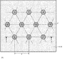
- FIG. 1A is a plan view showing a filler arrangement of a filler-containing film 1A of an example.
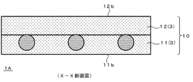
- FIG. 1B is a cross-sectional view of the filler-containing film 1A of the example.
- Drawing 2A is an explanatory view of the manufacturing method of filler content film 1A of an example.
- Drawing 2B is an explanatory view of the manufacturing method of filler content film 1A of an example.
- Drawing 2C is an explanatory view of the manufacturing method of filler content film 1A of an example.
- Drawing 2D is an explanatory view of the manufacturing method of filler content film 1A of an example.
- FIG. 2E is an explanatory diagram of a method for producing the filler-containing film 1A of the example.
- FIG. 1A is a plan view showing a filler arrangement of a filler-containing film 1A of an example.
- FIG. 1B is a cross-sectional view of the filler-containing film 1A of the example.
- Drawing 2A is
- FIG. 2F is an explanatory diagram of a method for producing the filler-containing film 1A of the example.
- FIG. 3 is a cross-sectional view of the filler-containing film 1B of the example.
- Drawing 4A is an explanatory view of the manufacturing method of filler content film 1B of an example.
- Drawing 4B is an explanatory view of the manufacturing method of filler content film 1B of an example.
- Drawing 4C is an explanatory view of the manufacturing method of filler content film 1B of an example.
- FIG. 5 is a cross-sectional view of the filler-containing film 1C of the example.
- Drawing 6 is an explanatory view of the manufacturing method of filler content film 1C of an example.
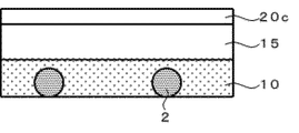
- FIG. 7 is a cross-sectional view of the filler-containing film 1D of the example.
- Drawing 8A is an explanatory view of the manufacturing method of filler content film 1D of an example.
- Drawing 8B is an explanatory view of the manufacturing method of filler content film 1D of an example.
- Drawing 8C is an explanatory view of the manufacturing method of filler content film 1D of an example.
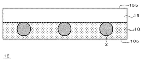
- FIG. 9 is a cross-sectional view of the filler-containing film 1E of the example.
- FIG. 10A is an explanatory diagram of a method for producing the filler-containing film 1E of the example.
- Drawing 10B is an explanatory view of the manufacturing method of filler content film 1E of an example.
- FIG. 10C is an explanatory diagram of a method for producing the filler-containing film 1E of the example.
- FIG. 11 is a perspective view of a sample for an adhesive strength test.
- FIG. 12 is an explanatory diagram of an adhesive strength test method.
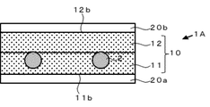
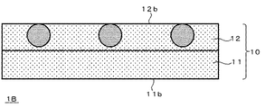
- FIG. 1A is a plan view showing the filler arrangement of the filler-containing film 1A of the example, and FIG. 1B is an XX cross-sectional view thereof.
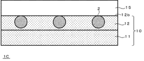
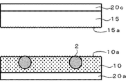
- This filler-containing film 1A contains conductive particles as the filler 2 and is used as an anisotropic conductive film. The conductive particles are held in the insulating resin layer 10 in a regular arrangement in which a predetermined arrangement is repeated. .
- the insulating resin layer 10 contains a fine solid 3 in addition to the filler 2.
- the regular filler arrangement before thermocompression spreads after thermocompression, and the repeated pitch of the array becomes wider than before thermocompression-bonding.
- the variation in the repeat pitch also increases, and the filler arrangement is disturbed.
- the filler movement amount and the array are less disturbed, and the filler repeat pitch after the thermocompression before the thermocompression is reduced.
- the ratio is within 300%, preferably within 250%, more preferably within 200%.
- the relative positional relationship of the filler arrangement is maintained before and after thermocompression, so that the distance between the centers of the nearest fillers before thermocompression is the closest after thermocompression.
- the distance between the centers of the fillers can be within 3 times, within 2.5 times, and within 2 times.
- the filler-containing film of the present invention has a thermocompression bonding condition in which the ratio of repeated pitches before and after thermocompression bonding is equal to or less than the above numerical value. This is because, according to the method for producing a filler-containing film of the present invention, since the surface of the filler-containing film 1A becomes a release surface from the release substrate, the insulating resin layer 10 contains a large amount of fine solids 3. However, the surface of the filler-containing film 1A does not become rough and becomes a smooth surface. When the smooth surface is attached to an article and heated and pressurized, the filler-containing film is uniformly pressed and regularly arranged in the film.
- the solid solids do not interfere with the pressing force being applied uniformly to the filler, and the filler arrangement is prevented from being disturbed unevenly, and the filler arrangement after heating and pressurization has expanded the original arrangement uniformly. This is considered to be because the portion where the ratio of the filler repeat pitch before and after thermocompression bonding is locally increased is reduced.
- thermocompression bonding is not performed on a smooth surface, nonuniformity occurs in the amount of filler movement and disorder of the thermocompression bonding. Therefore, when the filler-containing film is configured as an anisotropic conductive film, if the fine pitch bump array is thermocompression bonded with the anisotropic conductive film, the disorder of the filler array may be relatively large.
- the filler 2 depending on the use of the filler-containing film, known inorganic fillers (metal particles, metal oxide particles, metal nitride particles, etc.), organic fillers (resin particles, rubber particles, etc.), Filler in which organic and inorganic materials are mixed (for example, particles whose core is formed of a resin material and metal-plated on the surface (metal-coated resin particles), and in which insulating fine particles are attached to the surface of conductive particles The surface of the conductive particles is subjected to insulation treatment, etc.) according to the performance required for applications such as hardness and optical performance.
- inorganic fillers metal particles, metal oxide particles, metal nitride particles, etc.
- organic fillers resin particles, rubber particles, etc.
- Filler in which organic and inorganic materials are mixed for example, particles whose core is formed of a resin material and metal-plated on the surface (metal-coated resin particles), and in which insulating fine particles are attached to the surface of conductive particles
- a silica filler for example, in an optical film or a matte film, a silica filler, a titanium oxide filler, a styrene filler, an acrylic filler, a melamine filler, various titanates, and the like can be used.
- titanium oxide, magnesium titanate, zinc titanate, bismuth titanate, lanthanum oxide, calcium titanate, strontium titanate, barium titanate, barium zirconate titanate, lead zirconate titanate and mixtures thereof Etc. can be used.
- the adhesive film can contain polymer rubber particles, silicone rubber particles, and the like. In the conductive film and the anisotropic conductive film, conductive particles are contained.
- the conductive particles include metal particles such as nickel, cobalt, silver, copper, gold, and palladium, alloy particles such as solder, metal-coated resin particles, and metal-coated resin particles having insulating fine particles attached to the surface. . Two or more kinds can be used in combination. Among these, the metal-coated resin particles are preferable in that the resin particles repel after being connected, so that the contact with the terminal is easily maintained and the conduction performance is stabilized. In addition, the surface of the conductive particles may be subjected to an insulation treatment that does not hinder the conduction characteristics by a known technique.
- the particle diameter of the filler 2 can be determined according to the use of the filler-containing film.
- the particle diameter of the filler 2 in order to improve the indentation precision of the filler at the time of manufacture of a filler containing film, Preferably it is 1 micrometer or more, More preferably, it is 2.5 micrometers or more.
- the particle diameter in order to suppress the influence of the position shift of the filler at the time of manufacture of a filler containing film, Preferably it is 200 micrometers or less, More preferably, it is 50 micrometers or less.
- the particle diameter means an average particle diameter.
- the average particle diameter of the filler in the filler-containing film can be determined from a planar image or a cross-sectional image.
- the average particle size of the filler as raw material particles before being contained in the filler-containing film can be determined using a wet flow type particle size / shape analyzer FPIA-3000 (Malvern). When fine particles such as insulating fine particles are attached to the filler, the diameter not including the fine particles is defined as the particle size.
- CV value standard deviation / average
- the filler-containing film is easily pressed evenly when the filler-containing film is pressed onto the article, and the pressing force can be prevented from being concentrated locally. Therefore, when the filler-containing film is configured as an anisotropic conductive film, the stability of the connection is improved, and after the connection, the connection state can be accurately evaluated by observing the indentation or the sandwiched state of the filler. .
- the terminal size is relatively large (FOB etc.) or relatively small (COG etc.) It is possible to accurately confirm the connection state by observing the indentation and the state of sandwiching the conductive particles. Therefore, inspection after anisotropic connection becomes easy, and it can be expected to improve the productivity of the connection process.
- the filler has a regular arrangement in which a predetermined arrangement is repeated.
- the arrangement of the filler 2 is a hexagonal lattice arrangement. It has become.
- examples of the regular arrangement of the filler include a lattice arrangement such as a square lattice, a rectangular lattice, and an orthorhombic lattice. A plurality of grids having different shapes may be combined. Particle rows in which fillers are linearly arranged at predetermined intervals may be arranged in parallel at predetermined intervals.
- the region where the fillers are densely arranged and the region where the fillers are sparsely arranged may be regularly repeated.
- the unit which the fillers are contacting may comprise the regular repeating unit of a filler.
- the filler-containing film is an anisotropic conductive film, it is more preferable to arrange the conductive particles in a non-contact regular arrangement in order to achieve both capture stability and short-circuit suppression at the terminal.
- Whether or not the fillers are regularly arranged is, for example, whether or not a predetermined arrangement of the fillers is repeated in the longitudinal direction of the film (winding direction when the filler-containing film is used as a wound body). Can be determined by observing.
- the lattice axis or the arrangement axis of the arrangement may be parallel to or crossing at least one of the longitudinal direction of the filler-containing film and the direction perpendicular to the longitudinal direction, It can be determined according to the article to which the filler-containing film is pressure-bonded.
- the distance between the fillers can be determined according to the article to be connected and the use, and the number density of the fillers is usually 10 pieces / mm 2 or more and 100,000 pieces / mm 2 or less, preferably 30 pieces / mm 2. As described above, it can be appropriately determined within the range of 70000 pieces / mm 2 or less.
- the filler-containing film is an anisotropic conductive film
- the interparticle distance of the conductive particles used as the filler 2 is appropriately determined according to the size, shape, and terminal pitch of the terminals connected by the anisotropic conductive film. Can be determined.
- the number density of the conductive particles may be 30 / mm 2 or more, and preferably 150 to 70000 / mm 2 . Particularly in the case of fine pitch use, it is preferably 6000 to 42000 pieces / mm 2 , more preferably 10,000 to 40000 pieces / mm 2 , and still more preferably 15000 to 35000 pieces / mm 2 .
- the particle diameter of the conductive particles is 10 ⁇ m or more, the number density of the conductive particles is preferably 30 to 6000 / mm 2 .
- the filler area occupancy calculated by the following formula is 0.3% or more from the viewpoint of expressing the filler-containing effect.
- the area occupancy of the filler is 35% or less and more preferably 30% or less from the viewpoint of suppressing the thrust required for the pressing jig to press the filler-containing film to the article.
- Filler area occupancy (%) [number density of filler in plan view] ⁇ [average of plan view area of one filler] ⁇ 100
- the number density of the filler is obtained by observing with a metal microscope, and is also observed with image analysis software (for example, WinROOF (Mitani Corporation), A Image-kun (registered trademark) (Asahi Kasei Engineering Corporation), etc.). May be obtained by measuring.
- image analysis software for example, WinROOF (Mitani Corporation), A Image-kun (registered trademark) (Asahi Kasei Engineering Corporation), etc.
- the observation method and the measurement method are not limited to the above.
- the vertices of the fillers in the film thickness direction are flush with the surface of the insulating resin layer 10 or a plane parallel to the surface. Preferably it is. Thereby, it becomes easy to make the filler-containing film uniformly press-bonded to the article.
- Insulating resin layer 10 can contain various fine solids 3 having different formation materials from filler 2 in order to impart functions different from filler 2 to filler-containing film 1A.
- the fine solid 3 can contain a viscosity modifier, a thixotropic agent, a polymerization initiator, a coupling agent, a flame retardant, and the like. More specifically, examples of the viscosity modifier include silica powder and alumina powder.
- the filler 2 and the fine solid 3 when conductive particles are used as the filler 2 and the filler-containing film is an anisotropic conductive film, the fine solid as described in Patent Document 5 is used.
- the conductive particles are held in the insulating resin layer by kneading into the insulating resin layer and pushing the conductive particles into the insulating resin layer, the conductive particles and the fine solids are both distributed in the insulating resin layer. Can be easily distinguished by the state.
- the particle size of the fine solid 3 is preferably smaller than the particle size of the filler 2.
- the fine solid contained as a viscosity modifier preferably has an average particle size. Can be less than 1 ⁇ m, more preferably 5 nm to 0.3 ⁇ m, or preferably 1/3 to 1/2 of the average particle diameter of the conductive particles contained as filler.
- the fine solids are kneaded into the insulating resin layer and the conductive particles are pushed into the insulating resin layer.
- the anisotropic conductive film is manufactured by this, there is no particular limitation as long as the indentation of the conductive particles is not hindered.
- the fine solid is 3% by mass or more.
- the amount is 5% by mass or more, and the fine solid 3 is formed in the insulating resin layer 10 at a high concentration so that it is necessary to push in anisotropic conductive connection in two stages. It can be included.
- the content of the fine solid 3 is preferably 50% by mass or less, and 40% by mass or less with respect to the insulating resin layer 10 from the viewpoint of securing the fluidity necessary for the film for connecting electronic components. More preferred is 35% by mass or less.
- the insulating resin layer may be comprised from the single insulating resin layer, and may be comprised from the laminated body of the several insulating resin layer.
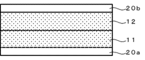
- the insulating resin layer 10 of the filler-containing film 1A shown in FIGS. 1A and 1B is obtained by applying the same insulating resin layer-forming composition onto a smooth release substrate by a method for producing a filler-containing film described later.
- the insulating resin layers 11 and 12 formed by drying are laminated with their dry surfaces on the inside and the surface on the peeling substrate side on the outside. In the filler-containing film 1A, the interface between the two insulating resin layers 11 and 12 can be observed.
- Roughness derived from fine solids contained in the composition is likely to appear on the surface coated with the insulating resin layer-forming composition and dried, but as shown in FIG. 1B, the insulating resin layer 11, When the coating and drying surface in No. 12 is overlapped, the surface of the filler-containing film becomes the surface to which the smooth surface of the release substrate is transferred, so that it is easy to thermocompression-bond the filler-containing film to the article uniformly. It is done.
- the resin composition forming the insulating resin layer 10 is appropriately selected according to the use of the filler-containing film, and can be formed from a thermoplastic resin composition, a high-viscosity adhesive resin composition, and a curable resin composition.
- the filler-containing film is an anisotropic conductive film, it is formed from a polymerizable compound and a polymerization initiator in the same manner as the resin composition forming the insulating resin layer of the anisotropic conductive film described in Patent Document 5.
- the curable resin composition to be used can be used.
- a thermal polymerization initiator may be used, a photopolymerization initiator may be used, or they may be used in combination.
- a cationic polymerization initiator is used as the thermal polymerization initiator
- an epoxy resin is used as the thermopolymerizable compound
- a radical photopolymerization initiator is used as the photopolymerization initiator
- an acrylate compound is used as the photopolymerizable compound.
- a thermal anionic polymerization initiator may be used as the thermal polymerization initiator.
- the thermal anionic polymerization initiator it is preferable to use a microcapsule-type latent curing agent formed by coating an imidazole-modified product as a nucleus and the surface thereof with polyurethane.
- the minimum melt viscosity of the insulating resin layer 10 is not particularly limited as long as the filler is pushed into the insulating resin layer, but in order to suppress unnecessary flow of the filler 2 when the filler-containing film 1A is thermocompression bonded to an article, It is preferably 1500 Pa ⁇ s or more, more preferably 2000 Pa ⁇ s or more, further preferably 3000 to 15000 Pa ⁇ s, and particularly preferably 3000 to 10000 Pa ⁇ s.
- This minimum melt viscosity can be determined by using a rotary rheometer (manufactured by TA instruments) as an example, and is kept constant at a measurement pressure of 5 g and using a measurement plate having a diameter of 8 mm. In a range of 30 to 200 ° C., the temperature can be obtained by setting the temperature rising rate to 10 ° C./min, the measurement frequency to 10 Hz, and the load fluctuation to the measurement plate of 5 g.
- the minimum melt viscosity can be adjusted by changing the kind and blending amount of the fine solids contained as the melt viscosity modifier, the adjustment conditions of the resin composition, and the like.
- the insulating resin layer may be composed of a single insulating resin layer, or may be composed of a laminate of a plurality of insulating resin layers.
- the thickness of the insulating resin layer is preferably relative to the particle diameter of the filler 2 so that the filler can be pushed in stably. 0.3 times or more, more preferably 0.6 times or more, further preferably 0.8 times or more, and particularly preferably 1 time or more.
- the upper limit of the thickness of the insulating resin layer is not particularly limited, and the layer thickness of the insulating resin layer may be appropriately adjusted according to the article to which the filler-containing film is thermocompression bonded. If the thickness is too thick, the filler 2 will be unnecessarily susceptible to the influence of the resin flow when the filler-containing film is thermocompression bonded to the article, and the absolute amount of fine solids contained in the insulating resin layer is large. As a result, the thermocompression bonding of the article may be hindered. Therefore, the layer thickness of the insulating resin layer is preferably 20 times or less, more preferably 15 times or less the particle diameter of the filler 2.
- the layer thickness of the low-viscosity resin layer depends on the use of the filler-containing film.
- the thickness of the filler 2 is preferably 0.2 times or more, more preferably 1 time or more, since the dispersion of the layer thickness becomes relatively large when the thickness is too thin.
- the particle diameter of the filler 2 is preferably 50 times or less, more preferably 15 times. Hereinafter, it is more preferably 8 times or less.
- the total thickness of these resin layers is the filler when the filler-containing film is thermocompression bonded to an article. From the point of suppression of unnecessary flow of 2, the point of suppression of protrusion and blocking of resin when winding a filler-containing film, the point of increasing the film length per unit weight of the filler-containing film, etc.
- the total thickness of the resin layer is preferably thinner. However, when it becomes too thin, the handleability of a filler containing film will be inferior. In addition, it may be difficult to stick the filler-containing film to the article.
- the total thickness of the resin layer in the filler-containing film is preferably 0.6 times or more, more preferably 0.8 times or more, further preferably 1 time or more, particularly preferably 1.times. 2 times or more.
- the upper limit of the total thickness of the resin layer including the insulating resin layer and the low-viscosity resin layer is not particularly limited, and may be appropriately adjusted according to the article to be thermocompression-bonded with the filler-containing film. If the total thickness becomes too thick, the filler 2 is easily affected by the resin flow when the filler-containing film is thermocompression bonded to the article, and the absolute amount of fine solids contained in the resin layer increases. Therefore, the total thickness of the resin layer is preferably 50 times or less, more preferably 15 times or less, and even more preferably 8 times or less the particle diameter of the filler 2. . It is considered that the influence of the resin flow on the filler arrangement can be minimized by making it 4 times or less, preferably 3 times or less.
- the conductive particles may be embedded in the insulating resin layer or exposed.
- the filler-containing film is configured as an anisotropic conductive film and the insulating resin layer and the low-viscosity resin layer are provided as the resin layer, the total thickness of the resin layer can be in the above range, but the electronic component to be connected In order to cope with the low profile of the bump, it is preferable to make the total thickness of the resin layer thinner than the above. In addition, by making the resin layer thin, the contact between the conductive particles and the bumps is facilitated.
- the lower limit of the total thickness of the resin layer is preferably 0.6 times or more, more preferably 0.8 times or more, and further preferably 1 time or more of the conductive particle diameter.
- the upper limit if it is too high, the thrust required at the time of indentation becomes too high, so that it can be 4 times or less the conductive particle diameter, preferably 3 times or less, more preferably 2 times or less, and still more preferably 1.8. It is not more than twice, particularly preferably not more than 1.5 times. What is necessary is just to adjust suitably about the ratio of the thickness of an insulating resin layer and a low-viscosity resin layer from relationships, such as an electroconductive particle diameter, bump height, and the adhesive force calculated
- the insulating resin layer has an adhesive force that enables temporary compression before thermocompression bonding to an article to be thermocompression bonded to the filler-containing film.
- the adhesive strength of the filler-containing film can be measured according to JIS Z 0237, and can also be measured as a tack force by a probe method according to JIS Z 3284-3 or ASTM D 2979-01.
- the tack force by the probe method on the front and back surfaces of the filler-containing film is, for example, When the pressing speed is 30 mm / min, the applied pressure is 196.25 gf, the pressing time is 1.0 sec, the peeling speed is 120 mm / min, and the measurement temperature is 23 ° C. ⁇ 5 ° C., at least one of the front and back surfaces is removed.
- 1.0kPa be a (0.1N / cm 2) or more, preferably to 1.5kPa (0.15N / cm 2) or more, and more to be higher than 3kPa (0.3N / cm 2) preferable.
- the tack force of the other surface may be measured by sticking one surface of the filler-containing film to the raw glass. Measurement may be performed by attaching to a flexible thermoplastic resin film (for example, a PET film having a thickness of 20 ⁇ m or less and not subjected to a release treatment, silicon rubber, etc.) instead of the raw glass. By reversing the surface to which the filler-containing film is attached, the tack force on the front and back surfaces of the filler-containing film can be measured under the same conditions.
- a flexible thermoplastic resin film for example, a PET film having a thickness of 20 ⁇ m or less and not subjected to a release treatment, silicon rubber, etc.
- the filler-containing film has release substrates on both front and back surfaces
- the filler-containing film has a release substrate on one side thereof, such as a filler-containing film formed into a wound body
- the surface on the release substrate side preferably exhibits the above-described tack force.
- a filler containing film has an insulating resin layer and a low-viscosity resin layer
- it is preferable that the surface of a low-viscosity resin layer has the above-mentioned tack force.
- the filler-containing film has a release substrate on both front and back surfaces, the surface pasted on the electronic component, or the surface on the side without the release substrate when the filler-containing film has a release substrate on one side,
- the surface on the insulating resin layer side when the filler-containing film has the insulating resin layer and the low-viscosity resin layer does not necessarily have the above-described tack force, but it is desirable to have it.
- the reason why the preferable tack force is different between the front and back surfaces of the filler-containing film is as follows.
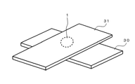
- the anisotropic conductive film is generally attached to the second electronic component such as a substrate on the side opposite to the peeling substrate and then peeled off.
- the substrate is peeled, and the first electronic component is mounted on the surface from which the peeling substrate is peeled (that is, the surface on the peeling substrate side). This is because it is necessary to ensure adhesive performance that can accurately fix the mounted component at this time.
- the necessary adhesive force may be determined according to the mounted component.
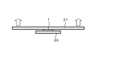
- the adhesive strength of the filler-containing film can also be determined according to the adhesive strength test described in JP-A-2017-48358. In this adhesive strength test, for example, when a filler-containing film is sandwiched between two glass plates, one glass plate is fixed, and the other glass plate is peeled off at a peeling speed of 10 mm / min and a test temperature of 50 ° C. In addition, by strengthening the adhesive state between the glass plate to be fixed and the filler-containing film, the adhesive force between the glass plate to be peeled off and the surface of the filler-containing film bonded to the glass plate is measured. Is possible.
- the adhesive force measured in this way can be preferably 1 N / cm 2 (10 kPa) or more, more preferably 10 N / cm 2 (100 kPa) or more.
- the adhesive strength of the filler-containing film can also be determined by a test in which the test piece is peeled off by aligning and bonding one end of the test piece and pulling up the other end.
- the adhesive force measured by this test method may be equivalent to the above-described adhesive strength test (1 N / cm 2 (10 kPa) or more).
- the adhesive strength in this test method can be 10% or more of the adhesive strength by the above-mentioned adhesive strength test. .
- the filler-containing film has the above-mentioned adhesive force, even if the article to be thermocompression bonded is, for example, an electronic component having a maximum dimension of less than 0.8 mm smaller than a general IC chip, the problem of misalignment in provisional pressure bonding is eliminated. Adhesion can be stabilized even with an electronic component having a maximum size of about 450 cm, which is the same as that of a large TV.
- Such adhesiveness adjusts the resin composition which comprises an insulating resin layer suitably, and improves the smoothness of the insulating resin layer which makes the outer surface of a filler containing film with the manufacturing method of the filler containing film mentioned later. By making it, it can provide to an insulating resin layer.
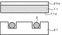
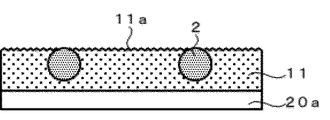
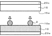
- the filler-containing film 1A can be manufactured as follows. First, the step of forming the insulating resin layer 11 by applying the above-described composition for forming an insulating resin layer containing a fine solid to a release substrate 20a having a smooth surface such as a PET film and drying it. Perform (FIG. 2A).
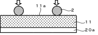
- the concave portion of the mold 21 in which the concave portion is formed corresponding to the regular arrangement of the filler 2 is filled with the filler 2 (FIG. 2B), transferring to the dry surface (surface opposite to the peeling substrate 20a) 11a of the insulating resin layer 11 (FIG. 2C), and performing a step of pushing the filler 2 into the insulating resin layer 11 (FIG. 2D). ).
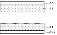
- the insulating resin layer 12 is formed on the peeling base material 20b in the same manner as the insulating resin layer 11, and the insulating resin layer 12 and the insulating resin layer 11 into which the above-mentioned filler is pressed are used.
- the peeling base materials 20a and 20b are opposed to each other (FIG. 2E), and a step of laminating them is performed (FIG. 2F).
- a filler-containing film 1A can be obtained (FIG. 1A).
- the filler 2 flows non-uniformly by thermocompression bonding, and the arrangement of the filler 2 after thermocompression bonding is an expansion of the original regular arrangement uniformly. Therefore, when the filler-containing film 1A is sandwiched between smooth surfaces and the area is subjected to thermocompression bonding under a predetermined heating and pressing condition according to the composition of the insulating resin layer, the repetition pitch of the filler after thermocompression bonding before thermocompression bonding The ratio is within 300%, which is significantly smaller than when the dry surfaces 11a and 12a of the insulating resin layer constitute the surface of the filler-containing film.
- thermocompression bonding conditions in which the ratio of the repetition pitch of the filler is within 300%, the temperature, pressure, and time can be easily selected because they can be appropriately selected from normal heating and pressing conditions in the insulating resin layer. Can do.
- a glass plate or the like As a smooth surface for sandwiching the filler-containing film when examining the ratio of the filler repeated pitch before and after thermocompression bonding, a glass plate or the like can be used, but the smooth surface of the article to be subjected to thermocompression bonding of the filler-containing film is used. May be.
- the filler-containing film is configured as an anisotropic conductive film
- smooth surfaces such as electrodes and bumps to be connected can be used. Thereby, the ratio of the repetition pitch of the conductive particles before and after thermocompression bonding in the electronic component to be connected can be evaluated.
- the area of the smooth surface when examining the ratio of the repeated pitches of the filler before and after thermocompression may be an area where the filler arrangement can be confirmed.
- the area can be an area in which at least one unit lattice or a repeating unit of a specific shape exists.
- the area where the unit cell is preferably 3 or more, more preferably 5 or more, and even more preferably 10 or more in the arrangement axis with the smallest filler pitch.
- the distance between the repeating units existing at the center is measured as the repetition pitch.
- the number of fillers is preferably 1000 or less, more preferably 500 or less, still more preferably 200 or less, and particularly preferably 50 or less. The area included in.
- the filler-containing film is configured as an anisotropic conductive film, and when evaluating the ratio of the repeated pitch of the conductive particles before and after thermocompression bonding, the smooth surface is, for example, a COG connection It is possible to use an input terminal having a relatively large area of the electronic component that performs the above. If the electronic component to be connected does not have a terminal having such an area, the evaluation may be performed using an electronic component having a terminal having such an area. As an example, a smooth surface of a terminal having a minimum one side of 30 ⁇ m or more, preferably 40 ⁇ m or more is used.
- N number The number of repeated pitch measurements (N number) is preferably 50 or more, and more preferably 100 or more. However, since such N number is difficult depending on the number density of the filler, it may be less.
- the measurement direction of the repetition pitch is a direction in which the ratio of the repetition pitch before and after the thermocompression bonding is increased.
- the actual repeat pitch ratio can be made equal to or less than the measured pitch ratio, and the accuracy of the filler arrangement can be confirmed.
- measurement points may be obtained by sampling in each measurement region. For example, 10% of the predetermined N number is measured in one region, and 10% of the N number is similarly measured in the other nine regions, and these are averaged. The number of regions where N number and N number are measured can be appropriately adjusted depending on the object to be thermocompression bonded.
- the amount of movement of the conductive particles may differ between the terminal flow direction and the direction perpendicular thereto. In this case, it is preferable to measure the pitch in the direction in which the amount of movement of the conductive particles is large.
- the terminal size and the distance between the terminals are large, and the amount of movement of the conductive particles in the terminal arrangement direction and the amount of movement of the conductive particles in the direction perpendicular thereto It is preferable to measure a pitch by selecting a portion having a small difference from the pitch. For example, in the case of COG connection, the terminal size and the distance between terminals are different between the input terminal and the output terminal. In that case, the pitch is measured at an input terminal having a large terminal size or a large distance between terminals. Thereby, it becomes easy to evaluate the movement amount of the conductive particles and the disorder of the arrangement.
- the above-described pitch measurement direction, measurement site, etc. when examining the ratio of the repeated pitch of the filler before and after thermocompression bonding can be the same even if the filler-containing film is other than the anisotropic conductive film.
- the ratio of the filler repeating pitch before and after thermocompression bonding with the article to be connected if the article does not have a smooth surface, it can be replaced with smooth glass plates.
- pitch measurement means examples include known image observation apparatuses such as an optical microscope, a metal microscope, and an electron microscope, and measurement systems such as WinROOF and A Image-kun (registered trademark), which can be appropriately combined.
- the smoothness of the surface is improved and the adhesiveness to the article is improved, so that the ratio of the repeated pitch of the filler after thermocompression bonding before thermocompression bonding is 300% as described above.
- the following can be reduced. Therefore, when the filler-containing film 1A is configured as an anisotropic conductive film, the temporary press bonding property of the anisotropic conductive film to the electronic component is improved, and the trapping property of the conductive particles at the terminal of the electronic component is improved also in the main press bonding. Short circuit is suppressed. Therefore, even when the terminal size of the electronic component is narrowed, it is possible to reliably conduct and suppress a short circuit.
- the improved adhesiveness stabilizes the mounting of electronic components that can be connected to both large and small electronic components, facilitates the manufacture of connectors, and improves productivity. it can.
- the need for precise alignment increases, so the filler-containing film of the present invention has a great effect.
- the filler-containing film of the present invention can take various forms.
- the filler-containing film 1B shown in FIG. 3 has a position on the film surface side of the filler 2 and the surface of the filler-containing film 1B (on the peeling substrate side of the insulating resin layer 12) with respect to the filler-containing film 1A described above. The difference is that the surface 12b) is flush with the film thickness direction.
- This filler-containing film 1B is a step of forming insulating resin layers 11 and 12 formed on the release substrates 20a and 20b (FIG. 4A), respectively, in the same manner as the manufacturing method of the filler-containing film 1A.
- 12 are laminated with the peeling base materials 20a and 20b on the outside (FIG. 4B), one peeling base material 20b is peeled, and the insulating resin after peeling is formed. It can manufacture by performing the process of pushing in the filler 2 from the surface 12b of the layer 12 (FIG. 4C).
- the surfaces 11b and 12b of the insulating resin layer forming the surface are smooth because the smoothness of the surfaces of the peeling base materials 20a and 20b is transferred, and is the same as the filler-containing film 1A. Demonstrate the effect.
- the filler-containing film 1C shown in FIG. 5 is obtained by laminating a low-viscosity resin layer 15 on the filler pressing surface (the surface 12b of the insulating resin layer on the peeling substrate side) (FIG. 4C) of the filler-containing form 1B. Is.
- the low viscosity resin layer 15 is a resin layer having a minimum melt viscosity in the range of 30 to 200 ° C. lower than that of the insulating resin layer 10.
- the low-viscosity resin layer 15 By laminating the low-viscosity resin layer 15 on the insulating resin layer 10, when two articles facing each other through the filler-containing film 1C are thermocompression bonded, their adhesiveness can be improved.
- 2 is used as conductive particles
- the filler-containing film 1C is used as an anisotropic conductive film, and when an electronic component is anisotropically conductively connected, the space formed by the electrodes and bumps of the electronic component is filled with the low-viscosity resin layer 15 And the adhesiveness of electronic components can be improved.
- the space between two articles connected via the filler-containing film 1C is filled with the low-viscosity resin layer 15 as the difference between the minimum melt viscosity of the insulating resin layer 10 and the minimum melt viscosity of the low-viscosity resin layer 15 increases. It becomes easy to be done. For this reason, when using the filler 2 as conductive particles and using the filler-containing film 1C as an anisotropic conductive film, the space formed by the electrodes and bumps of the electronic component is easily filled with the low-viscosity resin layer 15, It becomes easy to improve the adhesiveness between electronic components.
- the ratio (A1 / A2) of the minimum melt viscosity A1 of the insulating resin layer 10 and the minimum melt viscosity A2 of the low viscosity resin layer 15 is practically the ratio of the layer thickness of the insulating resin layer 10 and the low viscosity resin layer 15 However, it is preferably 2 or more, more preferably 5 or more, and still more preferably 8 or more. On the other hand, when this ratio is too large, when a long filler-containing film is used as a wound body, there is a possibility that the resin protrudes or blocks, and therefore, practically, 30 or less is preferable, and 15 or less is more preferable.
- the preferable minimum melt viscosity of the low-viscosity resin layer 15 more specifically satisfies the above-mentioned ratio, and is 3000 Pa ⁇ s or less, more preferably 2000 Pa ⁇ s or less, and particularly preferably 100 to 2000 Pa ⁇ s. .
- the low-viscosity resin layer 15 can be formed by adjusting the viscosity in the same resin composition as the insulating resin layer 10.
- the low-viscosity resin layer 15 can contain a fine solid as necessary.
- a composition for forming a low-viscosity resin layer is formed on a release substrate 20c such as a release film.
- the low-viscosity resin layer 15 is formed by coating and drying, and the dry surface 15a is opposed to the pressing surface of the filler 2 of the insulating resin layer 10, and the low-viscosity resin layer 15 is laminated on the insulating resin layer 10. be able to.
- the content of fine solids in the low-viscosity resin layer 15 is low and there is no substantial difference between the adhesiveness of the dry surface 15a of the low-viscosity resin layer 15 and the adhesiveness of the surface 15b on the opposite side. May apply the composition for low-viscosity resin layer formation directly to the pressing surface of the filler 2 of the insulating resin layer 10 to form the low-viscosity resin layer 15.
- the top of the filler 2 is flush with the outer surface of the insulating resin layer 10 of the laminate in which the dry surfaces of the insulating resin layer 10 and the low-viscosity resin layer 15 face each other. They are arranged together and can be manufactured from the next step.
- a composition for forming an insulating resin layer containing a minute solid is applied on the release substrate 20a and dried to form the insulating resin layer 10, and a composition for forming a low-viscosity resin layer is formed.
- An object is applied on the peeling substrate 20c and dried to form a low-viscosity resin layer 15 (FIG. 8A).
- the insulating resin layer 10 and the low-viscosity resin layer 15 are combined with each other.
- a step of forming a laminate of the insulating resin layer 10 and the low-viscosity resin layer 15 is performed by laminating the peeling base materials 20a and 20c outside (that is, with the dry surfaces facing each other) (FIG. 8B).
- the peeling substrate 20a of the insulating resin layer 10 is peeled from the laminate, and the filler 2 is pushed in from the surface of the insulating resin layer from which the peeling substrate is peeled (FIG. 8C).
- the surface 10b of the insulating resin layer and the surface 15b of the low-viscosity resin layer 15 forming the surfaces thereof are transferred by the smoothness of the surfaces of the release substrates 20a and 20c. It is smooth and exhibits the same effect as the filler-containing film 1A.
- the filler-containing film 1E shown in FIG. 9 has the top of the filler 2 on the dry surface of the insulating resin layer 10 of the laminate in which the dry surface of the insulating resin layer 10 and the dry surface of the low-viscosity resin layer 15 face each other. They are arranged flush with each other and can be manufactured from the next step.
- an insulating resin layer-forming composition containing fine solids is applied onto the release substrate 20a and dried to dry the insulating resin layer. 10 is performed, and the low-viscosity resin layer forming composition is applied onto the peeling substrate 20c and dried to form the low-viscosity resin layer 15 (FIG. 8A).
- the filler 2 is pushed into the dry surface 10a of the insulating resin layer 10 by performing a step of pushing the filler 2 from the surface (dry surface 10a) opposite to the release substrate 20a of the insulating resin layer 10 (FIG. 10A).
- the tops in the film thickness direction of 2 are flush with each other (FIG. 10B).
- the dry surface 10a and the dry surface 15a of the low-viscosity resin layer described above are laminated so as to face each other (FIG. 10C).
- the surface 10b of the insulating resin layer and the surface 15b of the low-viscosity resin layer 15 forming the surface are also smooth because the smoothness of the surfaces of the release substrates 20a and 20c is transferred. And exhibits the same effect as the filler-containing film 1A.
- the filler-containing film can be a wound body in its product form.
- it is 5000 m or less, More preferably, it is 1000 m or less, More preferably, it is 500 m or less. On the other hand, 5 m or more is preferable from the viewpoint of mass productivity of the wound body.
- the wound body may be formed by connecting filler-containing films shorter than the entire length.
- a connection place can exist in multiple places regularly or randomly.
- the film width in the wound body it is preferable to make the film width 0.3 mm or more from the lower limit of the slit width when slitting a wide filler-containing film to produce a wound body, More preferably, the slit width is 0.5 mm or more from the viewpoint of stabilizing the slit width.
- the slit width is 0.5 mm or more from the viewpoint of stabilizing the slit width.
- the film width is preferably selected from 0.3 to 400 mm depending on the connection object from the viewpoint of practical handling. That is, when an anisotropic conductive film is used at the end of an electronic article to be connected, the film width is often set to about several millimeters or less, and relatively large electronic components (electrode wiring and mounting portion are on one side). In the case where the film is used as it is attached to a substrate or a wafer before cutting), a film width of about 400 mm may be required. Generally, the anisotropic conductive film is often used with a film width of 0.5 to 5 mm.
- the filler-containing film of the present invention can be used by being attached to an article similarly to the conventional filler-containing film, and the article to be attached is not particularly limited. Therefore, various 1st components and 2nd components can be connected via a filler containing film, and the connection body of a 1st article and a 2nd article can be obtained.
- the anisotropic conductive film is converted into a semiconductor element using a PN junction using a thermocompression bonding tool (power generation element such as a solar cell, imaging element such as a CCD, Light-emitting elements, Peltier elements), other various semiconductor elements, IC chips, IC modules, FPCs and other first electronic components, and FPCs, glass substrates, plastic substrates, rigid substrates, ceramic substrates and other second electronic components
- a thermocompression bonding tool power generation element such as a solar cell, imaging element such as a CCD, Light-emitting elements, Peltier elements
- This filler-containing film can also be used for electronic parts for purposes other than anisotropic conductive connection.
- the surface of the article on which the filler-containing film is bonded may be smooth or may have a stepped portion or a convex shape.
- a filler containing film when using it for large sized TV etc., may be stuck 1 m or more, for example, 4.5 m or more to one side.
- the filler-containing film in addition to using the filler-containing film as an anisotropic conductive film, it may be used as a spacer film using a filler as a spacer.
- the IC chip or wafer may be stacked to make a multilayer by using the anisotropic conductive film of the present invention.
- the electronic component connected with the anisotropic conductive film of this invention is not limited to the illustration of the above-mentioned electronic component. It can be used for various electronic parts that have been diversified in recent years.
- the present invention includes a film adhesive body in which the filler-containing film of the present invention is bonded to various articles, and in particular, a connection in which the first electronic component and the second electronic component are connected via an anisotropic conductive film. Includes the body.
- the method for laminating the filler-containing film to the article may be pressure bonding, preferably thermocompression bonding depending on the use of the filler-containing film, and light irradiation may be used at the time of bonding.
- the first electronic component is an IC chip and the second electronic component is a substrate
- the first electronic is generally used.
- the component is placed on the pressure tool side
- the second electronic component is placed on the stage facing the first electronic component
- an anisotropic conductive film is pasted on the second electronic component in advance, and the first using the pressure tool.
- Thermocompression bonding of the electronic component and the second electronic component is performed.
- an anisotropic conductive film may be attached in advance to the first electronic component, and the first electronic component is not limited to the IC chip.
- the resin around the conductive particles may be removed in advance before the thermocompression bonding. Thereby, the influence of the resin flow generated when the anisotropic conductive film is thermocompression bonded to the electronic article can be reduced, and unnecessary flow of the conductive particles can be suppressed.
- thermocompression bonding as the main pressure bonding (hereinafter, not only the thermocompression bonding during the main pressure bonding).
- a connection method in which pressing is performed even by provisional pressure bonding is called connection by two-step pressing).
- WO2016 / 143789 describes that the connection is made by two-step indentation using an anisotropic conductive film in which conductive particles are randomly dispersed, but the conductive particles are regularly arranged as in the present invention.
- the number of these is not limited to one-to-one.
- a plurality of first electronic components are connected to one second electronic component.
- the present invention also includes a method for manufacturing a connection body in which the first electronic component and the second electronic component are connected via an anisotropic conductive film.
- Comparative Example 1 (1) Formation of Insulating Resin Layer An insulating resin layer forming composition is prepared with the formulation shown in Table 1, applied to a PET film, dried, and the insulating resin layer having the thickness shown in Table 2 (hereinafter, high viscosity) Resin layer).
- the metal-coated resin particles (Sekisui Chemical Co., Ltd., AUL703, average particle diameter 3 ⁇ m) described in Examples of Patent Document 5 are used as the conductive particles.
- the conductive particles were pressed into the dry surface of the high-viscosity resin layer by the method described in the Example of (1), which was adhered to the dry surface of the high-viscosity resin layer and pressed (60 ° C., 0.5 MPa). (Particle density 28000 / mm 2 ). In this case, the conductive particles were arranged in a hexagonal lattice, and the top in the film thickness direction was flush with the dry surface of the high viscosity resin layer.
- Example 1 A high viscosity resin layer was formed on the PET film in the same manner as in Comparative Example 1 (layer thickness: 3 ⁇ m).
- a composition for forming a low-viscosity resin layer was prepared with the formulation shown in Table 1, and applied to a PET film and dried to form a low-viscosity resin layer having a layer thickness of 3 ⁇ m.
- Minimum melt viscosity of this low-viscosity resin layer (rotary rheometer (manufactured by TA instruments), measurement pressure 5 g, temperature range 30 to 200 ° C., heating rate 10 ° C./min, measurement frequency 10 Hz, measurement plate diameter 8 mm, measurement plate The load fluctuation 5 g) was 300 Pa ⁇ s.
- the high-viscosity resin layer on the PET film and the low-viscosity resin layer on the PET film are bonded to each other to form a laminate of the high-viscosity resin layer and the low-viscosity resin layer.
- conductive particles were stuck and pressed into the surface of the high viscosity resin layer from which the PET film was peeled.
- Example 2 A high viscosity resin layer was formed on a PET film in the same manner as in Comparative Example 1, and conductive particles were pushed into the dried surface. On the other hand, a low-viscosity resin layer was formed on a PET film in the same manner as in Example 1, and this dry surface was bonded to the dry surface of the high-viscosity resin layer.
- Example 3 A high-viscosity resin layer was formed on the PET film in the same manner as in Comparative Example 1 (layer thickness 3 ⁇ m), and conductive particles were pushed in from the dried surface. Separately, a high-viscosity resin layer was separately formed on the PET film (layer thickness 3 ⁇ m), and the dry surfaces of both high-viscosity resin layers were bonded together.
- Example 4 A high viscosity resin layer was formed on the PET film in the same manner as in Comparative Example 1 (layer thickness: 3 ⁇ m). A similar high-viscosity resin layer was separately formed (layer thickness: 3 ⁇ m), and these dry surfaces were bonded together to form a laminate having two high-viscosity resin layers. One PET film of this laminate was peeled off, and conductive particles were stuck and pressed into the surface of the high viscosity resin layer from which the PET film was peeled in the same manner as in Comparative Example 1.
- Ratio of repeated pitch of particle arrangement before and after thermocompression bonding (%)
- the following electronic parts (a) and (b) are used as electronic parts for evaluation of the ratio of the repetition pitch of the particle arrangement before and after thermocompression bonding, and these electronic parts (a) and (b) are produced in examples and comparative examples.
- the bump area (0.0024 mm 2 ) containing at least 50 conductive particles was sandwiched by thermocompression bonding at a temperature of 180 ° C. and a pressure of 60 MPa for 5 seconds.
- the glass substrate of the electronic component (b) was disposed on the lower side in the figure, and the evaluation IC for the electronic component (a) was disposed on the upper side.
- the repetition pitch P0 of the conductive particles before thermocompression bonding and the repetition pitch P1 (distance between the centers of the conductive particles) (FIG. 1) of the conductive particles after thermocompression bonding are expressed by two axes per bump at the center of the bump area. Measured. That is, the axis having the shallowest angle (near parallel) with respect to the bump arrangement direction and a small movement amount of the resin (A axis) and the axis having the largest angle with respect to the bump arrangement direction and the large movement amount of the resin (B axis). ), The pitch P0 before thermocompression bonding was measured.
- This measurement was performed with 20 or more bumps in parallel, and the number of measurements for each of the A-axis and B-axis was set to 50, and the average of the pitches P0 was obtained for each axis.
- the pitch P1 after thermocompression bonding the number of measurements was set to 50 for each of the A axis and the B axis, and the average of the pitch P1 for each axis was obtained.
- the ratio ((P1 / P0) ⁇ 100%) before and after thermocompression bonding was determined for each of the A axis and B axis.
- Evaluation criteria OK The anisotropic conductive film does not peel from the glass substrate in all 100 times.
- NG The anisotropic conductive film peels from the glass substrate at least once out of 100 times.
- Example 1 and Example 2 when placed on a flat surface and the touch was confirmed with a finger, the adhesive force on the low viscosity resin layer side was larger than the adhesive force on the high viscosity resin layer side.
- the lower slide glass 30 is placed on a hot plate heated to 40 to 50 ° C., which is a general stage temperature for temporary attachment at the time of mounting, is pressed with a finger, heated for 30 seconds, and bonded together.
- the slide glass 30 and the lower surface of the anisotropic conductive film were in a so-called temporarily attached state.
- the upper slide glass 31 is placed on and bonded to the upper surface of the “film configuration” shown in Table 2, and the upper slide glass 31 is adhered by the adhesive force of the upper surface of the anisotropic conductive film. It was in the state.
- the lower slide glass 30 is fixed with a jig using an AGS-X series manufactured by Shimadzu Corporation.
- the value was divided by the area of the anisotropic conductive film 1 to obtain the adhesive strength of the upper surface of “Film Configuration” in Table 2.
- the adhesive strength test was performed twice, and the minimum value is shown in Table 2.
- a cylindrical 5 mm diameter probe (stainless steel mirror finish) of a tack tester is set above the measurement surface, and the probe is brought into contact with the measurement surface at a pressing speed of 30 mm / min, and a pressure of 196.25 gf is applied.
- the pressure is applied for 1.0 sec, the resistance that the probe receives due to the adhesive force of the measurement surface when it is peeled 2 mm from the measurement surface at a peeling speed of 120 mm / min is measured as a load value, and the probe is peeled off from the measurement surface
- the maximum load was the adhesive force (tack force).
- the adhesive strength was measured twice, and the minimum value is shown in Table 2. However, since the measurement in Examples 3 and 4 was difficult, the variation in measured values was larger than that in Examples 1 and 2. In Comparative Example 1, the adhesive strength was smaller than that in Examples 3 and 4 due to the touch feeling with a finger, and measurement was not performed.
- Examples 1 to 4 are superior to Comparative Example 1 in (2) film surface adhesion (temporary pressure bonding test).
- Examples 1 to 4 and Comparative Example 1 it can be seen that (3) initial conduction resistance and (4) conduction reliability are not problematic in Examples 1 to 4.
- the ratio of the pitch before and after thermocompression bonding ((P1 / P0) ⁇ 100%) on both the A axis and the B axis is 300% or less, and the arrangement before and after thermocompression bonding It was confirmed that there was little disturbance.
- the bumps and terminal patterns of the evaluation IC chip and the glass substrate correspond to each other. Moreover, when connecting the IC chip for evaluation and the glass substrate, the longitudinal direction of the anisotropic conductive film and the arrangement direction of the bumps were matched. In the two-step indentation, the temporary pressure bonding was performed at 80 ° C. for 3 seconds, and the final pressure bonding was performed at 180 ° C. for 10 seconds at twice the pressure of the temporary pressure bonding. In proceeding from the temporary pressure bonding to the main pressure bonding, the pressure applied to the evaluation IC chip was increased without releasing the pressure.
- a flip chip bonder (Panasonic FCB3, with pal heater) was used, and the temperature was raised to 0.5 seconds and the pressure was raised to 0.5 seconds in both the temporary pressure bonding and the main pressure bonding. Moreover, the connection body which performed only said main crimping
- connection body that was not pressed by the temporary pressure bonding was pressed in two steps (the pressure was increased without releasing the pressure after the temporary pressure bonding). It was confirmed that there are many conductive particles sandwiched per one.
Landscapes
- Chemical & Material Sciences (AREA)
- Organic Chemistry (AREA)
- Engineering & Computer Science (AREA)
- Chemical Kinetics & Catalysis (AREA)
- Computer Hardware Design (AREA)
- Microelectronics & Electronic Packaging (AREA)
- Power Engineering (AREA)
- Inorganic Chemistry (AREA)
- Health & Medical Sciences (AREA)
- Medicinal Chemistry (AREA)
- Polymers & Plastics (AREA)
- Manufacturing & Machinery (AREA)
- Laminated Bodies (AREA)
- Moulding By Coating Moulds (AREA)
- Adhesive Tapes (AREA)
- Adhesives Or Adhesive Processes (AREA)
- Non-Insulated Conductors (AREA)
- Manufacturing Of Electrical Connectors (AREA)
Priority Applications (4)
| Application Number | Priority Date | Filing Date | Title |
|---|---|---|---|
| CN201980037398.7A CN112292430A (zh) | 2018-06-06 | 2019-06-06 | 含有填料的膜 |
| US17/059,287 US20210238456A1 (en) | 2018-06-06 | 2019-06-06 | Filler-containing film |
| KR1020207033415A KR102729383B1 (ko) | 2018-06-06 | 2019-06-06 | 필러 함유 필름 |
| US18/971,478 US20250092288A1 (en) | 2018-06-06 | 2024-12-06 | Filler-containing film |
Applications Claiming Priority (4)
| Application Number | Priority Date | Filing Date | Title |
|---|---|---|---|
| JP2018109087 | 2018-06-06 | ||
| JP2018-109087 | 2018-06-06 | ||
| JP2019105900A JP7510039B2 (ja) | 2018-06-06 | 2019-06-06 | フィラー含有フィルム |
| JP2019-105900 | 2019-06-06 |
Related Child Applications (2)
| Application Number | Title | Priority Date | Filing Date |
|---|---|---|---|
| US17/059,287 A-371-Of-International US20210238456A1 (en) | 2018-06-06 | 2019-06-06 | Filler-containing film |
| US18/971,478 Division US20250092288A1 (en) | 2018-06-06 | 2024-12-06 | Filler-containing film |
Publications (1)
| Publication Number | Publication Date |
|---|---|
| WO2019235560A1 true WO2019235560A1 (ja) | 2019-12-12 |
Family
ID=68769392
Family Applications (1)
| Application Number | Title | Priority Date | Filing Date |
|---|---|---|---|
| PCT/JP2019/022492 Ceased WO2019235560A1 (ja) | 2018-06-06 | 2019-06-06 | フィラー含有フィルム |
Country Status (6)
| Country | Link |
|---|---|
| US (2) | US20210238456A1 (enExample) |
| JP (3) | JP7510039B2 (enExample) |
| KR (1) | KR102729383B1 (enExample) |
| CN (1) | CN112292430A (enExample) |
| TW (1) | TWI895244B (enExample) |
| WO (1) | WO2019235560A1 (enExample) |
Families Citing this family (5)
| Publication number | Priority date | Publication date | Assignee | Title |
|---|---|---|---|---|
| KR20250046348A (ko) * | 2018-06-26 | 2025-04-02 | 가부시끼가이샤 레조낙 | 땜납 입자 및 땜납 입자의 제조 방법 |
| KR102827173B1 (ko) | 2018-06-26 | 2025-06-27 | 가부시끼가이샤 레조낙 | 이방성 도전 필름과 그 제조 방법 및 접속 구조체의 제조 방법 |
| WO2020004513A1 (ja) | 2018-06-26 | 2020-01-02 | 日立化成株式会社 | はんだ粒子 |
| JP7400465B2 (ja) * | 2019-12-27 | 2023-12-19 | 株式会社レゾナック | コアシェル型はんだ粒子、コアシェル型はんだ粒子の製造方法、異方性導電フィルム、及び異方性導電フィルムの製造方法 |
| JPWO2022102573A1 (enExample) * | 2020-11-10 | 2022-05-19 |
Citations (5)
| Publication number | Priority date | Publication date | Assignee | Title |
|---|---|---|---|---|
| JP2015195198A (ja) * | 2014-03-20 | 2015-11-05 | デクセリアルズ株式会社 | 異方性導電フィルム及びその製造方法 |
| JP6187665B1 (ja) * | 2016-10-18 | 2017-08-30 | デクセリアルズ株式会社 | 異方性導電フィルム |
| JP2017204463A (ja) * | 2016-05-05 | 2017-11-16 | デクセリアルズ株式会社 | 異方性導電フィルム |
| JP2018078096A (ja) * | 2016-10-31 | 2018-05-17 | デクセリアルズ株式会社 | フィラー含有フィルム |
| JP2018081906A (ja) * | 2016-11-04 | 2018-05-24 | デクセリアルズ株式会社 | フィラー含有フィルム |
Family Cites Families (12)
| Publication number | Priority date | Publication date | Assignee | Title |
|---|---|---|---|---|
| JPH0221177Y2 (enExample) | 1984-11-10 | 1990-06-07 | ||
| JP2006015680A (ja) | 2004-07-05 | 2006-01-19 | Oike Ind Co Ltd | 艶消しフィルム |
| WO2007123003A1 (ja) * | 2006-04-12 | 2007-11-01 | Hitachi Chemical Company, Ltd. | 回路接続用接着フィルム、回路部材の接続構造及び回路部材の接続方法 |
| CN102723381B (zh) * | 2007-05-09 | 2015-08-19 | 日立化成株式会社 | 导电体连接用部件 |
| KR20100098459A (ko) * | 2008-04-28 | 2010-09-06 | 히다치 가세고교 가부시끼가이샤 | 회로 접속 재료, 필름상 접착제, 접착제 릴 및 회로 접속 구조체 |
| KR20110136731A (ko) * | 2010-06-14 | 2011-12-21 | 히다치 가세고교 가부시끼가이샤 | 회로 접속용 접착 필름 및 그의 용도, 회로 접속 구조체 및 그의 제조 방법 및 회로 부재의 접속 방법 |
| JP2013103368A (ja) | 2011-11-11 | 2013-05-30 | Sekisui Chem Co Ltd | 多層フィルム |
| JP6221285B2 (ja) | 2013-03-21 | 2017-11-01 | 日立化成株式会社 | 回路部材の接続方法 |
| JP6264897B2 (ja) | 2014-01-23 | 2018-01-24 | トヨタ自動車株式会社 | 高誘電率フィルム及びフィルムコンデンサ |
| JP6535989B2 (ja) | 2014-07-30 | 2019-07-03 | 日立化成株式会社 | 異方導電性フィルムの製造方法及び接続構造体 |
| WO2018074318A1 (ja) * | 2016-10-18 | 2018-04-26 | デクセリアルズ株式会社 | フィラー含有フィルム |
| WO2018079303A1 (ja) * | 2016-10-31 | 2018-05-03 | デクセリアルズ株式会社 | フィラー含有フィルム |
-
2019
- 2019-06-06 JP JP2019105900A patent/JP7510039B2/ja active Active
- 2019-06-06 US US17/059,287 patent/US20210238456A1/en not_active Abandoned
- 2019-06-06 CN CN201980037398.7A patent/CN112292430A/zh active Pending
- 2019-06-06 TW TW108119806A patent/TWI895244B/zh active
- 2019-06-06 WO PCT/JP2019/022492 patent/WO2019235560A1/ja not_active Ceased
- 2019-06-06 KR KR1020207033415A patent/KR102729383B1/ko active Active
-
2024
- 2024-01-30 JP JP2024012146A patent/JP7741420B2/ja active Active
- 2024-12-06 US US18/971,478 patent/US20250092288A1/en active Pending
-
2025
- 2025-09-03 JP JP2025145933A patent/JP2025174998A/ja active Pending
Patent Citations (5)
| Publication number | Priority date | Publication date | Assignee | Title |
|---|---|---|---|---|
| JP2015195198A (ja) * | 2014-03-20 | 2015-11-05 | デクセリアルズ株式会社 | 異方性導電フィルム及びその製造方法 |
| JP2017204463A (ja) * | 2016-05-05 | 2017-11-16 | デクセリアルズ株式会社 | 異方性導電フィルム |
| JP6187665B1 (ja) * | 2016-10-18 | 2017-08-30 | デクセリアルズ株式会社 | 異方性導電フィルム |
| JP2018078096A (ja) * | 2016-10-31 | 2018-05-17 | デクセリアルズ株式会社 | フィラー含有フィルム |
| JP2018081906A (ja) * | 2016-11-04 | 2018-05-24 | デクセリアルズ株式会社 | フィラー含有フィルム |
Also Published As
| Publication number | Publication date |
|---|---|
| JP7741420B2 (ja) | 2025-09-18 |
| TW202014305A (zh) | 2020-04-16 |
| US20250092288A1 (en) | 2025-03-20 |
| JP2019214714A (ja) | 2019-12-19 |
| US20210238456A1 (en) | 2021-08-05 |
| CN112292430A (zh) | 2021-01-29 |
| TWI895244B (zh) | 2025-09-01 |
| KR102729383B1 (ko) | 2024-11-12 |
| JP2024052743A (ja) | 2024-04-12 |
| JP2025174998A (ja) | 2025-11-28 |
| KR20210016523A (ko) | 2021-02-16 |
| JP7510039B2 (ja) | 2024-07-03 |
Similar Documents
| Publication | Publication Date | Title |
|---|---|---|
| JP7741420B2 (ja) | フィラー含有フィルム | |
| JP7330768B2 (ja) | 接続体の製造方法、接続方法 | |
| JP7313913B2 (ja) | 接続体、接続体の製造方法、接続方法 | |
| WO2023054259A1 (ja) | フィラー含有フィルム | |
| JP2023051250A (ja) | 接続構造体 | |
| HK40043312A (en) | Filler-containing film | |
| JP2024136131A (ja) | フィラー含有フィルム、接合体及びその製造方法 | |
| WO2024195598A1 (ja) | フィラー含有フィルム | |
| WO2019235589A1 (ja) | 接続体の製造方法、接続方法 | |
| WO2019235596A1 (ja) | 接続体、接続体の製造方法、接続方法 | |
| JP2024136135A (ja) | フィラー含有フィルム、接合体及びその製造方法 | |
| JP2024136139A (ja) | フィラー含有フィルム、接続体及びその製造方法 | |
| HK40043691A (en) | Connector, method for manufacturing connector, and connection method | |
| HK40043695A (en) | Method for manufacturing connector and connection method |
Legal Events
| Date | Code | Title | Description |
|---|---|---|---|
| 121 | Ep: the epo has been informed by wipo that ep was designated in this application |
Ref document number: 19815834 Country of ref document: EP Kind code of ref document: A1 |
|
| DPE1 | Request for preliminary examination filed after expiration of 19th month from priority date (pct application filed from 20040101) | ||
| NENP | Non-entry into the national phase |
Ref country code: DE |
|
| 122 | Ep: pct application non-entry in european phase |
Ref document number: 19815834 Country of ref document: EP Kind code of ref document: A1 |