WO2019235288A1 - 原子層成長法を用いて基板上に薄膜を成膜する方法、または装置 - Google Patents
原子層成長法を用いて基板上に薄膜を成膜する方法、または装置 Download PDFInfo
- Publication number
- WO2019235288A1 WO2019235288A1 PCT/JP2019/020933 JP2019020933W WO2019235288A1 WO 2019235288 A1 WO2019235288 A1 WO 2019235288A1 JP 2019020933 W JP2019020933 W JP 2019020933W WO 2019235288 A1 WO2019235288 A1 WO 2019235288A1
- Authority
- WO
- WIPO (PCT)
- Prior art keywords
- precursor
- gas
- supply
- substrate
- time
- Prior art date
- Legal status (The legal status is an assumption and is not a legal conclusion. Google has not performed a legal analysis and makes no representation as to the accuracy of the status listed.)
- Ceased
Links
- 0 CN(*)[Si]N(*)* Chemical compound CN(*)[Si]N(*)* 0.000 description 1
Images


Classifications
-
- H—ELECTRICITY
- H01—ELECTRIC ELEMENTS
- H01J—ELECTRIC DISCHARGE TUBES OR DISCHARGE LAMPS
- H01J37/00—Discharge tubes with provision for introducing objects or material to be exposed to the discharge, e.g. for the purpose of examination or processing thereof
- H01J37/32—Gas-filled discharge tubes
- H01J37/32431—Constructional details of the reactor
- H01J37/3244—Gas supply means
- H01J37/32449—Gas control, e.g. control of the gas flow
-
- C—CHEMISTRY; METALLURGY
- C23—COATING METALLIC MATERIAL; COATING MATERIAL WITH METALLIC MATERIAL; CHEMICAL SURFACE TREATMENT; DIFFUSION TREATMENT OF METALLIC MATERIAL; COATING BY VACUUM EVAPORATION, BY SPUTTERING, BY ION IMPLANTATION OR BY CHEMICAL VAPOUR DEPOSITION, IN GENERAL; INHIBITING CORROSION OF METALLIC MATERIAL OR INCRUSTATION IN GENERAL
- C23C—COATING METALLIC MATERIAL; COATING MATERIAL WITH METALLIC MATERIAL; SURFACE TREATMENT OF METALLIC MATERIAL BY DIFFUSION INTO THE SURFACE, BY CHEMICAL CONVERSION OR SUBSTITUTION; COATING BY VACUUM EVAPORATION, BY SPUTTERING, BY ION IMPLANTATION OR BY CHEMICAL VAPOUR DEPOSITION, IN GENERAL
- C23C16/00—Chemical coating by decomposition of gaseous compounds, without leaving reaction products of surface material in the coating, i.e. chemical vapour deposition [CVD] processes
- C23C16/22—Chemical coating by decomposition of gaseous compounds, without leaving reaction products of surface material in the coating, i.e. chemical vapour deposition [CVD] processes characterised by the deposition of inorganic material, other than metallic material
- C23C16/30—Deposition of compounds, mixtures or solid solutions, e.g. borides, carbides, nitrides
- C23C16/40—Oxides
- C23C16/401—Oxides containing silicon
-
- C—CHEMISTRY; METALLURGY
- C23—COATING METALLIC MATERIAL; COATING MATERIAL WITH METALLIC MATERIAL; CHEMICAL SURFACE TREATMENT; DIFFUSION TREATMENT OF METALLIC MATERIAL; COATING BY VACUUM EVAPORATION, BY SPUTTERING, BY ION IMPLANTATION OR BY CHEMICAL VAPOUR DEPOSITION, IN GENERAL; INHIBITING CORROSION OF METALLIC MATERIAL OR INCRUSTATION IN GENERAL
- C23C—COATING METALLIC MATERIAL; COATING MATERIAL WITH METALLIC MATERIAL; SURFACE TREATMENT OF METALLIC MATERIAL BY DIFFUSION INTO THE SURFACE, BY CHEMICAL CONVERSION OR SUBSTITUTION; COATING BY VACUUM EVAPORATION, BY SPUTTERING, BY ION IMPLANTATION OR BY CHEMICAL VAPOUR DEPOSITION, IN GENERAL
- C23C16/00—Chemical coating by decomposition of gaseous compounds, without leaving reaction products of surface material in the coating, i.e. chemical vapour deposition [CVD] processes
- C23C16/44—Chemical coating by decomposition of gaseous compounds, without leaving reaction products of surface material in the coating, i.e. chemical vapour deposition [CVD] processes characterised by the method of coating
- C23C16/455—Chemical coating by decomposition of gaseous compounds, without leaving reaction products of surface material in the coating, i.e. chemical vapour deposition [CVD] processes characterised by the method of coating characterised by the method used for introducing gases into reaction chamber or for modifying gas flows in reaction chamber
- C23C16/45523—Pulsed gas flow or change of composition over time
- C23C16/45525—Atomic layer deposition [ALD]
- C23C16/45527—Atomic layer deposition [ALD] characterized by the ALD cycle, e.g. different flows or temperatures during half-reactions, unusual pulsing sequence, use of precursor mixtures or auxiliary reactants or activations
- C23C16/45536—Use of plasma, radiation or electromagnetic fields
-
- C—CHEMISTRY; METALLURGY
- C23—COATING METALLIC MATERIAL; COATING MATERIAL WITH METALLIC MATERIAL; CHEMICAL SURFACE TREATMENT; DIFFUSION TREATMENT OF METALLIC MATERIAL; COATING BY VACUUM EVAPORATION, BY SPUTTERING, BY ION IMPLANTATION OR BY CHEMICAL VAPOUR DEPOSITION, IN GENERAL; INHIBITING CORROSION OF METALLIC MATERIAL OR INCRUSTATION IN GENERAL
- C23C—COATING METALLIC MATERIAL; COATING MATERIAL WITH METALLIC MATERIAL; SURFACE TREATMENT OF METALLIC MATERIAL BY DIFFUSION INTO THE SURFACE, BY CHEMICAL CONVERSION OR SUBSTITUTION; COATING BY VACUUM EVAPORATION, BY SPUTTERING, BY ION IMPLANTATION OR BY CHEMICAL VAPOUR DEPOSITION, IN GENERAL
- C23C16/00—Chemical coating by decomposition of gaseous compounds, without leaving reaction products of surface material in the coating, i.e. chemical vapour deposition [CVD] processes
- C23C16/44—Chemical coating by decomposition of gaseous compounds, without leaving reaction products of surface material in the coating, i.e. chemical vapour deposition [CVD] processes characterised by the method of coating
- C23C16/455—Chemical coating by decomposition of gaseous compounds, without leaving reaction products of surface material in the coating, i.e. chemical vapour deposition [CVD] processes characterised by the method of coating characterised by the method used for introducing gases into reaction chamber or for modifying gas flows in reaction chamber
- C23C16/45523—Pulsed gas flow or change of composition over time
- C23C16/45525—Atomic layer deposition [ALD]
- C23C16/45544—Atomic layer deposition [ALD] characterized by the apparatus
-
- C—CHEMISTRY; METALLURGY
- C23—COATING METALLIC MATERIAL; COATING MATERIAL WITH METALLIC MATERIAL; CHEMICAL SURFACE TREATMENT; DIFFUSION TREATMENT OF METALLIC MATERIAL; COATING BY VACUUM EVAPORATION, BY SPUTTERING, BY ION IMPLANTATION OR BY CHEMICAL VAPOUR DEPOSITION, IN GENERAL; INHIBITING CORROSION OF METALLIC MATERIAL OR INCRUSTATION IN GENERAL
- C23C—COATING METALLIC MATERIAL; COATING MATERIAL WITH METALLIC MATERIAL; SURFACE TREATMENT OF METALLIC MATERIAL BY DIFFUSION INTO THE SURFACE, BY CHEMICAL CONVERSION OR SUBSTITUTION; COATING BY VACUUM EVAPORATION, BY SPUTTERING, BY ION IMPLANTATION OR BY CHEMICAL VAPOUR DEPOSITION, IN GENERAL
- C23C16/00—Chemical coating by decomposition of gaseous compounds, without leaving reaction products of surface material in the coating, i.e. chemical vapour deposition [CVD] processes
- C23C16/44—Chemical coating by decomposition of gaseous compounds, without leaving reaction products of surface material in the coating, i.e. chemical vapour deposition [CVD] processes characterised by the method of coating
- C23C16/455—Chemical coating by decomposition of gaseous compounds, without leaving reaction products of surface material in the coating, i.e. chemical vapour deposition [CVD] processes characterised by the method of coating characterised by the method used for introducing gases into reaction chamber or for modifying gas flows in reaction chamber
- C23C16/45523—Pulsed gas flow or change of composition over time
- C23C16/45525—Atomic layer deposition [ALD]
- C23C16/45553—Atomic layer deposition [ALD] characterized by the use of precursors specially adapted for ALD
-
- C—CHEMISTRY; METALLURGY
- C23—COATING METALLIC MATERIAL; COATING MATERIAL WITH METALLIC MATERIAL; CHEMICAL SURFACE TREATMENT; DIFFUSION TREATMENT OF METALLIC MATERIAL; COATING BY VACUUM EVAPORATION, BY SPUTTERING, BY ION IMPLANTATION OR BY CHEMICAL VAPOUR DEPOSITION, IN GENERAL; INHIBITING CORROSION OF METALLIC MATERIAL OR INCRUSTATION IN GENERAL
- C23C—COATING METALLIC MATERIAL; COATING MATERIAL WITH METALLIC MATERIAL; SURFACE TREATMENT OF METALLIC MATERIAL BY DIFFUSION INTO THE SURFACE, BY CHEMICAL CONVERSION OR SUBSTITUTION; COATING BY VACUUM EVAPORATION, BY SPUTTERING, BY ION IMPLANTATION OR BY CHEMICAL VAPOUR DEPOSITION, IN GENERAL
- C23C16/00—Chemical coating by decomposition of gaseous compounds, without leaving reaction products of surface material in the coating, i.e. chemical vapour deposition [CVD] processes
- C23C16/44—Chemical coating by decomposition of gaseous compounds, without leaving reaction products of surface material in the coating, i.e. chemical vapour deposition [CVD] processes characterised by the method of coating
- C23C16/455—Chemical coating by decomposition of gaseous compounds, without leaving reaction products of surface material in the coating, i.e. chemical vapour deposition [CVD] processes characterised by the method of coating characterised by the method used for introducing gases into reaction chamber or for modifying gas flows in reaction chamber
- C23C16/45561—Gas plumbing upstream of the reaction chamber
-
- C—CHEMISTRY; METALLURGY
- C23—COATING METALLIC MATERIAL; COATING MATERIAL WITH METALLIC MATERIAL; CHEMICAL SURFACE TREATMENT; DIFFUSION TREATMENT OF METALLIC MATERIAL; COATING BY VACUUM EVAPORATION, BY SPUTTERING, BY ION IMPLANTATION OR BY CHEMICAL VAPOUR DEPOSITION, IN GENERAL; INHIBITING CORROSION OF METALLIC MATERIAL OR INCRUSTATION IN GENERAL
- C23C—COATING METALLIC MATERIAL; COATING MATERIAL WITH METALLIC MATERIAL; SURFACE TREATMENT OF METALLIC MATERIAL BY DIFFUSION INTO THE SURFACE, BY CHEMICAL CONVERSION OR SUBSTITUTION; COATING BY VACUUM EVAPORATION, BY SPUTTERING, BY ION IMPLANTATION OR BY CHEMICAL VAPOUR DEPOSITION, IN GENERAL
- C23C16/00—Chemical coating by decomposition of gaseous compounds, without leaving reaction products of surface material in the coating, i.e. chemical vapour deposition [CVD] processes
- C23C16/44—Chemical coating by decomposition of gaseous compounds, without leaving reaction products of surface material in the coating, i.e. chemical vapour deposition [CVD] processes characterised by the method of coating
- C23C16/455—Chemical coating by decomposition of gaseous compounds, without leaving reaction products of surface material in the coating, i.e. chemical vapour deposition [CVD] processes characterised by the method of coating characterised by the method used for introducing gases into reaction chamber or for modifying gas flows in reaction chamber
- C23C16/45563—Gas nozzles
- C23C16/45574—Nozzles for more than one gas
-
- C—CHEMISTRY; METALLURGY
- C23—COATING METALLIC MATERIAL; COATING MATERIAL WITH METALLIC MATERIAL; CHEMICAL SURFACE TREATMENT; DIFFUSION TREATMENT OF METALLIC MATERIAL; COATING BY VACUUM EVAPORATION, BY SPUTTERING, BY ION IMPLANTATION OR BY CHEMICAL VAPOUR DEPOSITION, IN GENERAL; INHIBITING CORROSION OF METALLIC MATERIAL OR INCRUSTATION IN GENERAL
- C23C—COATING METALLIC MATERIAL; COATING MATERIAL WITH METALLIC MATERIAL; SURFACE TREATMENT OF METALLIC MATERIAL BY DIFFUSION INTO THE SURFACE, BY CHEMICAL CONVERSION OR SUBSTITUTION; COATING BY VACUUM EVAPORATION, BY SPUTTERING, BY ION IMPLANTATION OR BY CHEMICAL VAPOUR DEPOSITION, IN GENERAL
- C23C16/00—Chemical coating by decomposition of gaseous compounds, without leaving reaction products of surface material in the coating, i.e. chemical vapour deposition [CVD] processes
- C23C16/44—Chemical coating by decomposition of gaseous compounds, without leaving reaction products of surface material in the coating, i.e. chemical vapour deposition [CVD] processes characterised by the method of coating
- C23C16/52—Controlling or regulating the coating process
-
- H—ELECTRICITY
- H01—ELECTRIC ELEMENTS
- H01J—ELECTRIC DISCHARGE TUBES OR DISCHARGE LAMPS
- H01J37/00—Discharge tubes with provision for introducing objects or material to be exposed to the discharge, e.g. for the purpose of examination or processing thereof
- H01J37/32—Gas-filled discharge tubes
- H01J37/32009—Arrangements for generation of plasma specially adapted for examination or treatment of objects, e.g. plasma sources
- H01J37/32082—Radio frequency generated discharge
- H01J37/32091—Radio frequency generated discharge the radio frequency energy being capacitively coupled to the plasma
-
- H—ELECTRICITY
- H01—ELECTRIC ELEMENTS
- H01L—SEMICONDUCTOR DEVICES NOT COVERED BY CLASS H10
- H01L21/00—Processes or apparatus adapted for the manufacture or treatment of semiconductor or solid state devices or of parts thereof
- H01L21/02—Manufacture or treatment of semiconductor devices or of parts thereof
- H01L21/02104—Forming layers
- H01L21/02107—Forming insulating materials on a substrate
- H01L21/02109—Forming insulating materials on a substrate characterised by the type of layer, e.g. type of material, porous/non-porous, pre-cursors, mixtures or laminates
- H01L21/02112—Forming insulating materials on a substrate characterised by the type of layer, e.g. type of material, porous/non-porous, pre-cursors, mixtures or laminates characterised by the material of the layer
- H01L21/02123—Forming insulating materials on a substrate characterised by the type of layer, e.g. type of material, porous/non-porous, pre-cursors, mixtures or laminates characterised by the material of the layer the material containing silicon
- H01L21/02164—Forming insulating materials on a substrate characterised by the type of layer, e.g. type of material, porous/non-porous, pre-cursors, mixtures or laminates characterised by the material of the layer the material containing silicon the material being a silicon oxide, e.g. SiO2
-
- H—ELECTRICITY
- H01—ELECTRIC ELEMENTS
- H01L—SEMICONDUCTOR DEVICES NOT COVERED BY CLASS H10
- H01L21/00—Processes or apparatus adapted for the manufacture or treatment of semiconductor or solid state devices or of parts thereof
- H01L21/02—Manufacture or treatment of semiconductor devices or of parts thereof
- H01L21/02104—Forming layers
- H01L21/02107—Forming insulating materials on a substrate
- H01L21/02109—Forming insulating materials on a substrate characterised by the type of layer, e.g. type of material, porous/non-porous, pre-cursors, mixtures or laminates
- H01L21/02112—Forming insulating materials on a substrate characterised by the type of layer, e.g. type of material, porous/non-porous, pre-cursors, mixtures or laminates characterised by the material of the layer
- H01L21/02123—Forming insulating materials on a substrate characterised by the type of layer, e.g. type of material, porous/non-porous, pre-cursors, mixtures or laminates characterised by the material of the layer the material containing silicon
- H01L21/0217—Forming insulating materials on a substrate characterised by the type of layer, e.g. type of material, porous/non-porous, pre-cursors, mixtures or laminates characterised by the material of the layer the material containing silicon the material being a silicon nitride not containing oxygen, e.g. SixNy or SixByNz
-
- H—ELECTRICITY
- H01—ELECTRIC ELEMENTS
- H01L—SEMICONDUCTOR DEVICES NOT COVERED BY CLASS H10
- H01L21/00—Processes or apparatus adapted for the manufacture or treatment of semiconductor or solid state devices or of parts thereof
- H01L21/02—Manufacture or treatment of semiconductor devices or of parts thereof
- H01L21/02104—Forming layers
- H01L21/02107—Forming insulating materials on a substrate
- H01L21/02109—Forming insulating materials on a substrate characterised by the type of layer, e.g. type of material, porous/non-porous, pre-cursors, mixtures or laminates
- H01L21/022—Forming insulating materials on a substrate characterised by the type of layer, e.g. type of material, porous/non-porous, pre-cursors, mixtures or laminates the layer being a laminate, i.e. composed of sublayers, e.g. stacks of alternating high-k metal oxides
-
- H—ELECTRICITY
- H01—ELECTRIC ELEMENTS
- H01L—SEMICONDUCTOR DEVICES NOT COVERED BY CLASS H10
- H01L21/00—Processes or apparatus adapted for the manufacture or treatment of semiconductor or solid state devices or of parts thereof
- H01L21/02—Manufacture or treatment of semiconductor devices or of parts thereof
- H01L21/02104—Forming layers
- H01L21/02107—Forming insulating materials on a substrate
- H01L21/02109—Forming insulating materials on a substrate characterised by the type of layer, e.g. type of material, porous/non-porous, pre-cursors, mixtures or laminates
- H01L21/02205—Forming insulating materials on a substrate characterised by the type of layer, e.g. type of material, porous/non-porous, pre-cursors, mixtures or laminates the layer being characterised by the precursor material for deposition
- H01L21/02208—Forming insulating materials on a substrate characterised by the type of layer, e.g. type of material, porous/non-porous, pre-cursors, mixtures or laminates the layer being characterised by the precursor material for deposition the precursor containing a compound comprising Si
- H01L21/02211—Forming insulating materials on a substrate characterised by the type of layer, e.g. type of material, porous/non-porous, pre-cursors, mixtures or laminates the layer being characterised by the precursor material for deposition the precursor containing a compound comprising Si the compound being a silane, e.g. disilane, methylsilane or chlorosilane
-
- H—ELECTRICITY
- H01—ELECTRIC ELEMENTS
- H01L—SEMICONDUCTOR DEVICES NOT COVERED BY CLASS H10
- H01L21/00—Processes or apparatus adapted for the manufacture or treatment of semiconductor or solid state devices or of parts thereof
- H01L21/02—Manufacture or treatment of semiconductor devices or of parts thereof
- H01L21/02104—Forming layers
- H01L21/02107—Forming insulating materials on a substrate
- H01L21/02109—Forming insulating materials on a substrate characterised by the type of layer, e.g. type of material, porous/non-porous, pre-cursors, mixtures or laminates
- H01L21/02205—Forming insulating materials on a substrate characterised by the type of layer, e.g. type of material, porous/non-porous, pre-cursors, mixtures or laminates the layer being characterised by the precursor material for deposition
- H01L21/02208—Forming insulating materials on a substrate characterised by the type of layer, e.g. type of material, porous/non-porous, pre-cursors, mixtures or laminates the layer being characterised by the precursor material for deposition the precursor containing a compound comprising Si
- H01L21/02219—Forming insulating materials on a substrate characterised by the type of layer, e.g. type of material, porous/non-porous, pre-cursors, mixtures or laminates the layer being characterised by the precursor material for deposition the precursor containing a compound comprising Si the compound comprising silicon and nitrogen
-
- H—ELECTRICITY
- H01—ELECTRIC ELEMENTS
- H01L—SEMICONDUCTOR DEVICES NOT COVERED BY CLASS H10
- H01L21/00—Processes or apparatus adapted for the manufacture or treatment of semiconductor or solid state devices or of parts thereof
- H01L21/02—Manufacture or treatment of semiconductor devices or of parts thereof
- H01L21/02104—Forming layers
- H01L21/02107—Forming insulating materials on a substrate
- H01L21/02225—Forming insulating materials on a substrate characterised by the process for the formation of the insulating layer
- H01L21/0226—Forming insulating materials on a substrate characterised by the process for the formation of the insulating layer formation by a deposition process
- H01L21/02263—Forming insulating materials on a substrate characterised by the process for the formation of the insulating layer formation by a deposition process deposition from the gas or vapour phase
- H01L21/02271—Forming insulating materials on a substrate characterised by the process for the formation of the insulating layer formation by a deposition process deposition from the gas or vapour phase deposition by decomposition or reaction of gaseous or vapour phase compounds, i.e. chemical vapour deposition
- H01L21/02274—Forming insulating materials on a substrate characterised by the process for the formation of the insulating layer formation by a deposition process deposition from the gas or vapour phase deposition by decomposition or reaction of gaseous or vapour phase compounds, i.e. chemical vapour deposition in the presence of a plasma [PECVD]
-
- H—ELECTRICITY
- H01—ELECTRIC ELEMENTS
- H01L—SEMICONDUCTOR DEVICES NOT COVERED BY CLASS H10
- H01L21/00—Processes or apparatus adapted for the manufacture or treatment of semiconductor or solid state devices or of parts thereof
- H01L21/02—Manufacture or treatment of semiconductor devices or of parts thereof
- H01L21/02104—Forming layers
- H01L21/02107—Forming insulating materials on a substrate
- H01L21/02225—Forming insulating materials on a substrate characterised by the process for the formation of the insulating layer
- H01L21/0226—Forming insulating materials on a substrate characterised by the process for the formation of the insulating layer formation by a deposition process
- H01L21/02263—Forming insulating materials on a substrate characterised by the process for the formation of the insulating layer formation by a deposition process deposition from the gas or vapour phase
- H01L21/02271—Forming insulating materials on a substrate characterised by the process for the formation of the insulating layer formation by a deposition process deposition from the gas or vapour phase deposition by decomposition or reaction of gaseous or vapour phase compounds, i.e. chemical vapour deposition
- H01L21/0228—Forming insulating materials on a substrate characterised by the process for the formation of the insulating layer formation by a deposition process deposition from the gas or vapour phase deposition by decomposition or reaction of gaseous or vapour phase compounds, i.e. chemical vapour deposition deposition by cyclic CVD, e.g. ALD, ALE, pulsed CVD
-
- H—ELECTRICITY
- H01—ELECTRIC ELEMENTS
- H01L—SEMICONDUCTOR DEVICES NOT COVERED BY CLASS H10
- H01L21/00—Processes or apparatus adapted for the manufacture or treatment of semiconductor or solid state devices or of parts thereof
- H01L21/67—Apparatus specially adapted for handling semiconductor or electric solid state devices during manufacture or treatment thereof; Apparatus specially adapted for handling wafers during manufacture or treatment of semiconductor or electric solid state devices or components ; Apparatus not specifically provided for elsewhere
- H01L21/683—Apparatus specially adapted for handling semiconductor or electric solid state devices during manufacture or treatment thereof; Apparatus specially adapted for handling wafers during manufacture or treatment of semiconductor or electric solid state devices or components ; Apparatus not specifically provided for elsewhere for supporting or gripping
- H01L21/687—Apparatus specially adapted for handling semiconductor or electric solid state devices during manufacture or treatment thereof; Apparatus specially adapted for handling wafers during manufacture or treatment of semiconductor or electric solid state devices or components ; Apparatus not specifically provided for elsewhere for supporting or gripping using mechanical means, e.g. chucks, clamps or pinches
- H01L21/68714—Apparatus specially adapted for handling semiconductor or electric solid state devices during manufacture or treatment thereof; Apparatus specially adapted for handling wafers during manufacture or treatment of semiconductor or electric solid state devices or components ; Apparatus not specifically provided for elsewhere for supporting or gripping using mechanical means, e.g. chucks, clamps or pinches the wafers being placed on a susceptor, stage or support
- H01L21/68742—Apparatus specially adapted for handling semiconductor or electric solid state devices during manufacture or treatment thereof; Apparatus specially adapted for handling wafers during manufacture or treatment of semiconductor or electric solid state devices or components ; Apparatus not specifically provided for elsewhere for supporting or gripping using mechanical means, e.g. chucks, clamps or pinches the wafers being placed on a susceptor, stage or support characterised by a lifting arrangement, e.g. lift pins
-
- H—ELECTRICITY
- H01—ELECTRIC ELEMENTS
- H01J—ELECTRIC DISCHARGE TUBES OR DISCHARGE LAMPS
- H01J2237/00—Discharge tubes exposing object to beam, e.g. for analysis treatment, etching, imaging
- H01J2237/32—Processing objects by plasma generation
- H01J2237/33—Processing objects by plasma generation characterised by the type of processing
- H01J2237/332—Coating
- H01J2237/3321—CVD [Chemical Vapor Deposition]
Definitions
- the present disclosure relates to a method or apparatus for forming a thin film on a substrate using an atomic layer growth method.
- ALD atomic growth method
- ALD using this film forming apparatus, first, a raw material gas is supplied into a processing container to adsorb the raw material gas onto a wafer. Next, a reactive gas is supplied into the processing container, and high-frequency power is applied between the electrodes to form plasma to activate the reactive gas, thereby reacting the active species of the reactive gas with the source gas adsorbed on the wafer.
- a thin film having a desired film thickness can be formed by repeating a plurality of cycles in which the source gas and the reaction gas are alternately supplied. In this ALD process, it may be required to control the film thickness distribution in the wafer surface.
- Patent Document 1 describes a technique for forming a silicon nitride film or a silicon oxide film using alkylaminosilane.
- alkylaminosilane is supplied after the substrate is irradiated with ammonia plasma or oxygen plasma.
- ammonia radicals or oxygen-containing radicals on the substrate surface are reacted with alkylaminosilane to form a silicon nitride film or a silicon oxide film.
- Patent Document 1 shows an ALD saturation curve showing the relationship between the deposition time and the pulse supply time of alkylaminosilane (here, diisopropylaminosilane (DIPAS)).
- DIPAS diisopropylaminosilane
- Patent Document 2 discloses a technique for improving the uniformity of the composition in the film thickness direction of the third metal oxide film in forming the third metal oxide film containing the first metal element and the second metal element. Has been described. In this technique, a metal oxide film containing a metal element having a larger composition ratio of the first metal element and the second metal element is formed in a saturation mode, and a metal oxide containing a metal element having a smaller composition ratio is formed. The film is formed in the unsaturated mode.
- This disclosure provides a technique with high film thickness controllability when forming a thin film on a substrate.
- One aspect of the present disclosure is: A method of forming a thin film on a substrate using an atomic layer growth method, Providing a precursor which is an aminosilane having one amino group to the substrate; The supply time of the precursor in the step is less than a time when the amount of adsorption of the precursor to the substrate reaches saturation.
- controllability of the film thickness can be enhanced when forming a thin film on the substrate.
- a film forming apparatus 1 which is an embodiment of the apparatus of the present disclosure will be described with reference to a longitudinal side view of FIG.
- the film forming apparatus 1 supplies a source gas and a reactive gas alternately and repeatedly into a processing container 11 that stores and processes a wafer W, and a thin film is formed by atomic layer deposition (ALD). It is configured to form a film.
- ALD atomic layer deposition
- the source gas a gas containing a precursor which is an aminosilane having one amino group is used.
- An example of this precursor is diisopropylaminosilane (SiH 3 N (CH (CH 3 ) 2 ) 2 : DIPAS).
- an oxidizing gas such as oxygen (O 2 ) gas or ozone (O 3 ) gas can be used.
- the processing vessel 11 has a generally flat circular shape, and a wafer loading / unloading port 12 and a gate valve 13 for opening and closing the loading / unloading port 12 are provided on the side wall.
- An exhaust duct 14 that forms a part of the side wall of the processing container 11 is provided above the loading / unloading port 12.
- a slit-like opening 15 extending along the circumferential direction is formed on the inner peripheral surface of the exhaust duct 14, and forms an exhaust port of the processing container 11.
- One end of an exhaust pipe 16 is connected to the exhaust duct 14, and the other end of the exhaust pipe 16 is connected to an exhaust mechanism 17 including a vacuum pump via a pressure adjustment mechanism 171 and a valve 172.
- a disk-shaped mounting part 31 for mounting the wafer W horizontally is provided in the processing container 11.
- a heater for heating the wafer W and a grounded electrode plate are embedded in the mounting portion 31.
- the heater and electrode plate are not shown.
- An upper end of a support member 34 that extends through the bottom of the processing container 11 and extends in the vertical direction is connected to the center portion on the lower surface side of the mounting portion 31, and a lower end of the support member 34 is connected to an elevating mechanism 35. With this lifting mechanism 35, the mounting portion 31 can move up and down between a lower position indicated by a chain line in FIG. 1 and an upper position indicated by a solid line in FIG.
- the position on the lower side is a delivery position for delivering the wafer W to / from a transfer mechanism (not shown) for the wafer W entering the processing container 11 from the loading / unloading port 12. Further, the upper position is a processing position where a film forming process is performed on the wafer W.
- Numeral 36 in FIG. 1 is a flange, and 37 is an expandable / contractible bellows.
- Reference numeral 38 in the figure is a support pin for the wafer W, and for example, three pins are provided (only two are shown in the figure).
- reference numeral 39 in FIG. 1 denotes an elevating mechanism that elevates and lowers the support pin 38.
- the gas discharge unit 4 On the upper side of the exhaust duct 14, the gas discharge unit 4 is provided so as to face the wafer W mounted on the mounting unit 31.
- the gas discharge unit 4 in this example includes a top plate member 41 provided so as to close the inside of the processing container 11 from above, and a shower plate 42 provided on the lower surface side of the top plate member 41.
- the shower plate 42 is formed in a disc shape and is disposed so as to face the placement portion 31.
- a flat circular gas diffusion space 43 is formed between the top plate member 41 and the shower plate 42.
- the shower plate 42 is formed with a large number of gas discharge holes 45 that are open toward the gas diffusion space 43.
- the peripheral edge of the shower plate 42 is supported by an annular protrusion 44 that protrudes downward from the lower surface of the top plate member 41.
- the lower end portion of the annular protrusion 44 protrudes to a position close to the upper surface on the peripheral side of the placement portion 31 disposed at the processing position.
- the gas discharge section 4 is formed with a plurality of concentric sections in which the gas discharge holes 45 are arranged concentrically corresponding to the radial direction of the wafer W, and a plurality of partition areas that can discharge gas independently of each other. ing.
- the gas diffusion space 43 is divided into a plurality of concentric circles by the partition wall 46 in correspondence with the radial direction of the wafer W placed on the placement table 31. . That is, when viewed from the mounting table 31 side, the array region of the large number of gas discharge holes 45 in the shower plate 42 is divided into three partition regions (a first partition region Z1, a second partition region Z2, and a second partition region). It is partitioned into a third partition region Z3).
- the partitioned regions of the gas diffusion space 43 in the gas discharge unit 4 are also referred to as first to third partitioned regions Z1 to Z3.
- the first to third partition regions Z1 to Z3 divide the circular shower plate 42 concentrically when viewed in plan, and the first partition region Z1 has a circular shape, the second and third partitions.
- the regions Z2 and Z3 are each formed in an annular shape.
- the gas diffusion space 43 is not limited to being completely concentrically partitioned, and may be partitioned into ellipses or rectangles to form these partition regions Z1 to Z3.
- the gas discharge unit 4 is provided with a precursor supply unit 50 that supplies a precursor that is a source gas, and a reaction gas supply unit 60 that supplies an O 2 gas that is a reaction gas. From the precursor supply unit 50 and the reaction gas supply unit 60, the precursor and the reaction gas are supplied to each of the partitioned regions Z1 to Z3 independently of each other.
- process gas supply paths 51, 52, and 53 are formed in the top plate member 41 of the gas discharge section 4 for supplying precursors and reaction gases to the partitioned regions Z1 to Z3.
- purge gas supply paths 61, 62, and 63 are formed in the top plate member 41 for supplying purge gas to the partition regions Z1 to Z3.
- the numbers of the processing gas supply paths 51, 52, and 53 and the purge gas supply paths 61, 62, and 63 shown in FIGS. 1 and 2 are examples. Actually, the necessary number of processing gas supply paths 51, 52, 53 and purge gas supply paths 61, 62, 63 are provided in the first to third partition regions Z1 to Z3 as appropriate.
- a raw material gas, a reactive gas, and a carrier gas are supplied to the processing gas supply paths 51, 52, and 53 via the supply control device 7.
- the supply control device 7 includes a precursor, a supply path for a reactive gas and a carrier gas, a flow rate adjusting unit including a valve, a mass flow controller, and the like.
- the processing gas supply paths 51, 52, and 53 are precursors (denoted as “PE (Precursor of Example)” in FIGS. 1 and 2) via the precursor supply paths 541, 542, and 543, respectively. Connected to source 54.
- the precursor supply passages 541, 542, and 543 are respectively provided with valves V11, V12, and V13 for the precursor supply operation, and flow rate adjusting units M11, M12, and M13.
- the processing gas supply paths 51, 52, and 53 are also connected to a supply source 55 for Ar gas that is a carrier gas via precursor supply paths 541, 542, and 543 and a carrier gas supply path 551, respectively.
- the carrier gas supply path 551 is provided with carrier gas supply valves V21, V22, V23, and flow rate adjusting units M21, M22, M23, respectively.
- the processing gas supply paths 51, 52, and 53 are connected to a reaction gas (O 2 gas) supply source 56 via reaction gas supply paths 561, 562, and 563, respectively.
- the reaction gas supply paths 561, 562, and 563 are provided with valves V31, V32, and V33, and flow rate adjustment units M31, M32, and M33, respectively, for supplying the reaction gas.
- the processing gas supply paths 51, 52, 53 are also connected to a carrier gas supply source 55 via reaction gas supply paths 561, 562, 563 and a carrier gas supply path 552, respectively.
- the carrier gas supply path 552 is provided with valves V41, V42 and V43 for supplying carrier gas, and flow rate adjusting units M41, M42 and M43, respectively.
- the process gas supply paths 51, 52 and 53, the precursor supply paths 541, 542 and 543, the valves V11, V12 and V13, the flow rate adjusting units M11, M12 and M13, and the precursor supply source 54 are used.
- Part 50 is configured.
- the process gas supply paths 51, 52, 53, the reaction gas supply paths 561, 562, 563, the valves V 31, V 32, V 33, the flow rate adjustment units M 31, M 32, M 33, and the reaction gas supply source 56 are used. Is configured.
- the purge gas supply paths 61, 62, and 63 merge with the supply path 553 on the way, for example, and are connected to a supply source 55 of Ar gas that is a purge gas via a valve V 5 and a mass flow controller M 5.
- the operation of each valve and the flow rate adjusting unit is controlled by the control unit 10 described later.
- the precursor supply valves V11, V12, and V13 are opened.
- the reaction gas supply valves V31, V32, and V33 are opened.
- the valves V21, V22, V23 or valves V41, V42, V43 for Ar gas supply are opened.
- the precursor or the reaction gas diluted with a predetermined amount of the carrier gas passes through the precursor supply passages 541 to 543 and the processing gas supply passages 51 to 53, and thereby the first to third partitioned regions of the gas diffusion space 43. Supplied to Z1 to Z3, respectively.
- the precursor or the reactive gas is discharged into the processing space 40 from the gas discharge holes 45 formed in the partition regions Z1 to Z3 of the shower plate 42, respectively.
- the precursor or reaction gas discharged from the partition regions Z1 to Z3 is supplied to the adsorption region of the wafer W facing the partition regions Z1 to Z3 of the shower plate 42. That is, a plurality of suction regions that are concentrically partitioned in the radial direction are formed in regions facing the partition regions Z1 to Z3 in the plane of the wafer W. For this reason, if the discharge flow rate of the precursor per unit area is made different between the first to third partition regions Z1 to Z3 on the gas discharge unit 4 side, the wafer W is between the three adsorption regions of W. The flow rate (supply flow rate) of the precursor supplied per unit area is different. Further, if the discharge time of the precursor is made different between the first to third partition regions Z1 to Z3 on the gas discharge unit 4 side, the supply time of the precursor is set between the three adsorption regions on the wafer W side. Will be different.
- a space surrounded by the lower surface of the shower plate 42 and the annular protrusion 44 and the upper surface of the mounting portion 31 forms a processing space 40 in which the film forming process is performed.
- the shower plate 42 is paired with an electrode plate (not shown) of the mounting portion 31 and is configured as an electrode plate for forming capacitively coupled plasma (CCP) in the processing space 40.
- a high frequency power supply 47 is connected to the shower plate 42 via a matching unit (not shown).
- the CCP is formed by supplying high-frequency power from the high-frequency power source 47 to the gas supplied to the processing space 40 via the shower plate 42.
- the shower plate 42, the electrode plate, and the high frequency power source 47 constitute a plasma generation mechanism. Instead of the shower plate 42, a high frequency power supply 47 may be connected to the electrode plate on the mounting portion 31 side, and the shower plate 42 may be grounded.
- control unit 10 including a computer.
- the control unit 10 includes a data processing unit including a program, a memory, and a CPU.
- the program incorporates instructions so that a control signal can be sent from the control unit 10 to each unit of the film forming apparatus 1 and a film forming process described later can be executed. Specifically, the opening / closing timing of each valve, the on / off timing of the high frequency power supply 47, the heating temperature of the wafer W by the heater, and the like are controlled by the above program.
- These programs are stored in a storage medium such as a compact disk, a hard disk, or an MO (magneto-optical disk) and installed in the control unit 10.
- control unit 10 is configured to output a control signal for adjusting the discharge time of the precursor from the gas discharge unit 4 to be less than the time when the adsorption amount of the precursor to the wafer W reaches saturation. Yes.
- control unit 10 performs control to make at least one of the precursor discharge flow rate and the discharge time per unit area different between at least two of the plurality of partition regions Z1 to Z3 of the gas discharge unit 4. It is configured to output a signal.
- the control unit 10 is configured to output a control signal for converting the O 2 gas into plasma by the plasma generation mechanism when the O 2 gas that is the reaction gas is discharged from the gas discharge unit 4. .
- the supply time of the precursor is a time for which the amount of adsorption of the precursor on the wafer W reaches saturation (hereinafter referred to as “saturation”).
- saturation a time for which the amount of adsorption of the precursor on the wafer W reaches saturation
- the silicon substrate includes silicon (Si) whose surface (surface on which the precursor is adsorbed) is terminated with a hydroxy group (OH group).
- a hydroxy group OH group
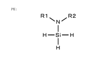
- aminosilane as a precursor is supplied, the amino group of aminosilane (NH 2 group, primary amino group (NHR1 group), secondary amino group (NR1R2 group), R1 and R2 in the description of this paragraph are hydrogen. And the hydrogen (H) of the hydroxy group is bonded and eliminated.
- oxygen (O) on the surface of the wafer W and the precursor silicon (Si) are combined, and the precursor is adsorbed.
- the reaction gas O 2 gas is supplied to form plasma
- the precursor adsorbed on the wafer W is oxidized by the active species of O 2 generated by the plasma, and the molecular layer of the silicon oxide film (SiO) One layer is formed.
- a SiO thin film (SiO film) having a desired film thickness is formed.
- the use of the O 3 gas as the reaction gas, plasma is generated, may be performed oxide precursors.
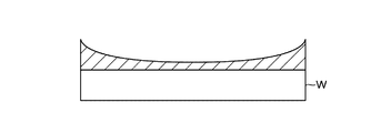
- FIG. 3 is a characteristic diagram schematically showing the relationship between the radial position of the wafer W and the partial pressure of the precursor.
- the horizontal axis indicates the position in the diameter direction of the wafer W
- the vertical axis indicates the partial pressure p of the precursor
- the horizontal axis O indicates the center of the wafer W.
- the adsorption amount of the precursor is reflected in the film thickness. For this reason, as shown in FIG. 3, if the precursor is supplied such that the partial pressure of the precursor is larger on the peripheral side than the center of the wafer in the radial direction of the wafer W, the amount of adsorption of the precursor also depends on the partial pressure. Change. As a result, the film thickness of the SiO film viewed along the radial direction of the wafer W is larger at the peripheral portion than at the central portion under conditions where the supply times of the source gases are uniform.
- the supply time of the precursor is controlled to be less than the time when the amount of adsorption of the precursor to the wafer W reaches saturation.
- saturation refers to the maximum amount of the precursor that can be adsorbed on the adsorption site on the surface of the wafer W.
- aminosilane reacts with and adsorbs to a hydroxy group (OH group) on the surface of the silicon substrate, so that the adsorption site becomes a hydroxy group.
- FIG. 4 schematically shows the relationship between the dose of the precursor in one cycle and the film formation rate per cycle.
- the horizontal axis Dz represents the dose amount
- the vertical axis GPC represents the film formation rate ( ⁇ / cycle).
- the dose is the amount of precursor supplied per unit area (mg / cm 2 ).
- the deposition rate increases as the dose increases, but when the dose exceeds a certain amount D1, the deposition rate becomes substantially constant. At this time, it is considered that a saturated amount of precursor is adsorbed on the surface of the wafer W. For this reason, in the region where the dose amount is D1 or more, the film thickness does not change even if the dose amount is increased. Therefore, in order to control the film thickness by adjusting the dose amount of the precursor, it is necessary to adjust the dose amount in a region smaller than D1.
- the state is “saturated” is confirmed experimentally from a state in which the deposition rate does not increase any more even if the dose of the precursor in one cycle is increased. You can also. From the above, the present disclosure can ensure film thickness controllability by adjusting the precursor supply time to be less than the saturation adsorption time. However, in the correspondence relationship between the actual dose amount and the GPC, the film forming speed is not completely constant, and the GPC may continue to slightly increase as the dose amount increases.
- the time during which the amount of increase in film formation rate (GPC) when the supply time is increased by unit time with the precursor supply flow rate being constant is 0.05 ⁇ / second is substantially A slight increase in GPC may be ignored as a typical “saturation adsorption time”.
- an aminosilane having one amino group is selected as a precursor having good controllability.
- An aminosilane having one amino group is an aminosilane having only one amino group and does not include an aminosilane having two or more amino groups. Specifically, it is represented by SiH 3 NR1R2 as shown in the structural formula of FIG. 6A.
- R1, R2 is a hydrogen group, a saturated chain hydrocarbon group, an unsaturated chain hydrocarbon group, a saturated cyclic hydrocarbon group, an aromatic hydrocarbon group, a halogen group, a hydroxy group, a carboxyl group, an ester group, An acyl group etc. can be illustrated.
- aminosilane having one amino group SiH 3 NH 2 , SiH 3 (N (CH 3 ) 2 ), SiH 3 (NH (CH 3 )), SiH 3 (N (CH 2 CH 3) 2 ), SiH 3 (NCH 3 (CH 2 CH 3 )), SiH 3 (NH (CH 2 CH 3 )), SiH 3 (N (CH 2 CH 2 CH 3 ) 2 ), SiH 3 (NH (CH 2 CH 2 CH 3)), SiH 3 (NHCH (CH 3) 2), SiH 3 (N (C (CH 3) 3) 2), can be exemplified SiH 3 (NHC (CH 3) 3).
- the number of silicon atoms contained in aminosilane having one amino group is not limited to one, but diisopropylaminodisilane (SiH 3 SiH 2 (N (CH (CH 3 ) 2 ) 2 )): amino such as DIPADS Disilane or aminotrisilane can also be used.
- FIG. 5 schematically shows the difference in controllability between different precursors.
- the horizontal axis Dz is the dose
- the vertical axis GPC is the film deposition rate ( ⁇ / cycle).
- PE is the precursor of the example
- PC Precursor of Comparative
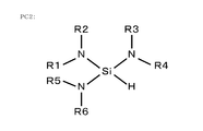
- the precursor of the example is an aminosilane having one amino group
- the precursor of the comparative example is an aminosilane having two or three amino groups.
- the aminosilane having two amino groups here means an aminosilane having only two amino groups
- the aminosilane having three amino groups means an aminosilane having only three amino groups. .
- the shape of the curve indicating the increase in the deposition rate with respect to the increase in the dose varies greatly depending on the type of precursor (the experimental results shown in FIG. 13 are also shown). reference).
- the shape of the curve indicates the controllability of the film thickness.
- the film thickness range FTe of the example PE is larger than the film thickness range FTc of the comparative example PC, and the curve of the non-saturation region is steep, so that by using the precursor of the example PE, the film It is understood that the controllability of the thickness is increased.
- the precursor having a plurality of amino groups in the process of adsorbing the precursor to the wafer W has a large number of amino groups, so even if adsorption sites where the precursor can be adsorbed remain, it is adsorbed by steric hindrance. It is easy to become incapable.
- an aminosilane having one amino group has a relatively small steric hindrance compared to a precursor having a plurality of amino groups, and the adsorption amount at the time of saturation accompanying the reaction with a hydroxyl group on the wafer surface. It is assumed that there are many.
- the fact that the adsorption amount at the time of saturation is large means that the adjustment amount of the adsorption amount at the time of non-saturation is large, suggesting that the adjustment range of the film thickness is large and the controllability is high.
- FIGS. 7 and 8 show an example of a film forming method of the present disclosure that is performed in the film forming apparatus 1 with reference to FIGS. 7 and 8.
- the processing is performed under the condition that the film thickness distribution at the peripheral portion of the wafer is larger than that at the central portion.
- the chart of FIG. 7 shows the start and stop timings of various gas supplies into the processing container 11 and the on / off timing of the high-frequency power supply 47 (plasma).
- the gate valve 13 is opened in a state where the inside of the processing vessel 11 is in a predetermined vacuum atmosphere, and the wafer is transferred from the transfer chamber in the vacuum atmosphere adjacent to the processing vessel 11 onto the placement unit 31 located at the delivery position by the transfer mechanism.
- Transport W When the wafer W is transferred to the placement unit 31 by raising and lowering the support pins 38 and the transfer mechanism is withdrawn from the processing container 11, the gate valve 13 is closed and the placement unit 31 is raised to the processing position for processing. A space 40 is formed. Further, the wafer W is heated to a predetermined temperature by the heater of the mounting portion 31.
- valves V 21 to V 23 and V 41 to V 43 are opened, and Ar gas is supplied from the supply source 55 to the processing space 40.
- valves V11 to V13 are opened, and DIPAS as a precursor is discharged from the supply source 54 into the processing space 40 through the gas discharge holes 45 of the first to third partition regions Z1 to Z3.
- the precursor is supplied to the wafer W, and the precursor is adsorbed on the surface of the wafer W (step S11).
- the supply time of the precursor to the wafer W in one cycle RC is less than the saturation adsorption time described above.
- the supply time to the first partition region Z1 is the shortest in the gas discharge unit 4,
- the precursor is supplied so that the supply time becomes longer toward the third partition region Z3 at the peripheral edge.
- the supply time of the precursor to the adsorption region facing the first partition region Z1 is the shortest, and the adsorption region and the third partition region Z3 facing the second partition region Z2.
- the supply time becomes longer as it goes to the suction area opposite to.
- FIG. 8 schematically shows that the partition regions Z1 to Z3 with long arrows are provided with a longer supply time, and the dose of the precursor in the opposing adsorption region increases.
- the valves V11 to V13 are closed, and the supply of the precursor to the wafer W is stopped.
- the precursor remaining in the processing space 40 and not adsorbed on the wafer W is purged with Ar gas (step S12).
- the precursor supply unit 50 supplies the mixed gas of the Ar gas and the precursor as the carrier gas during the precursor supply time period, and continues to supply the Ar gas during other than the precursor supply time period. To do. Thereby, the backflow of the precursor and the reaction gas to the processing gas supply paths 51 to 53, the precursor supply paths 541 to 543, and the reaction gas supply paths 561 to 563 is prevented.
- the valves V31 to V33 are opened, and the reactive gas is discharged from the reactive gas supply source 56 into the processing space 40 through the gas discharge holes 45 of the first to third partitioned regions Z1 to Z3, and the high frequency power supply 47 is turned on. turn on.
- the supply time of the reaction gas at this time is the shortest supply time to the first partition region Z1 when the supply flow rates of the reaction gas and Ar gas are the same, and the third partition region Control is performed so that the supply time becomes longer toward Z3.
- the O 2 gas that is the reaction gas in the processing space 40 is turned into plasma, and the precursor adsorbed on the wafer W is oxidized by this plasma, and a layer of SiO is formed as a reaction product (step S13).
- the high frequency power supply 47 is turned off and the valves V31 to V33 are closed to stop the formation of plasma and the supply of the reaction gas in the processing space 40.
- the reactive gas remaining in the processing space 40 and the activated species of the deactivated plasma are purged with Ar gas and removed from the processing space 40 (step S14).
- the reactive gas supply unit 60 supplies the mixed gas of Ar gas and the reactive gas as the carrier gas during the reactive gas supply time period, and supplies Ar gas during the reactive gas supply time period. Configured to continue. Thereby, the backflow of the precursor and the reaction gas to the processing gas supply paths 51 to 53, the precursor supply paths 541 to 543, and the reaction gas supply paths 561 to 563 is prevented.
- Steps S11 to S14 are repeated a set number of times, the placement unit 31 descends, and the wafer W is unloaded from the processing container 11 in the reverse order of loading into the processing container 11 to form a film forming process. Ends.
- the above-described method of forming a SiO film by ALD is an example, and a step in which only O 2 gas that has not been converted to plasma flows may be inserted between steps S12 and S13.
- one film formation cycle is carried out by supplying the precursor ⁇ continuous supply of the purge gas ⁇ supply of the O 2 gas ⁇ supply of O 2 gas and generation of SiO by generation of plasma ⁇ continuous supply of the purge gas.
- O 2 gas that is a reactive gas may be constantly supplied during the film forming process.
- the O 2 gas and the purge gas are continuously supplied, and the precursor supply ⁇ the continuous supply of the O 2 gas and the purge gas ⁇ the generation of SiO by the generation of the plasma ⁇ the continuous supply of the O 2 gas and the purge gas A film formation cycle is performed.
- the precursor when the precursor is supplied, a mixed gas of the precursor, the carrier gas, the purge gas, and the O 2 gas becomes the source gas. Therefore, the partial pressure of the precursor in the source gas can be adjusted by the mixing ratio of the precursor, the carrier gas, and the O 2 gas.
- an aminosilane having one amino group is selected as the precursor, and the supply time of the precursor allocated in one cycle is the time for the adsorption amount of the precursor to the wafer W to reach saturation ( Saturation adsorption time) is set. For this reason, as described above, the change in the film thickness with respect to the change in the dose can be kept large, and the controllability of the film thickness can be improved.
- the supply time of the precursor is set to be different between at least two adsorption regions among the plurality of adsorption regions of the wafer W.
- the supply time of the precursor and the reactive gas is controlled so that the central portion of the wafer W is shortest and becomes longer toward the peripheral portion.
- an SiO film having a film thickness distribution in which the film thickness at the peripheral edge is thicker than that at the center can be formed in the wafer surface.
- the film thickness distribution can be controlled by increasing the film thickness in the region where the supply time is long and decreasing the film thickness in the region where the supply time is short.
- the supply flow rate of the precursor per unit area is different. In this way, the film thickness distribution may be controlled.
- This supply flow rate can be adjusted by changing the partial pressure (concentration) of the precursor in the gas when the discharge time of the gas discharged from each of the partition regions Z1 to Z3 is the same. As a result, on the wafer W side, the mass flow rate [mg / cm 2 ⁇ sec] of the precursor per unit area is adjusted.
- a plurality of gas discharge holes 45 arranged in a concentric manner corresponding to the radial direction of the wafer W, and a plurality of gas discharge holes can be discharged independently of each other.
- a partitioned area is formed.
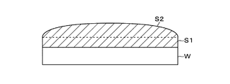
- the thin film in this example is formed by laminating a flat film S1 on the wafer W and a film S2 having a film thickness distribution in which the film thickness in the central part is larger than that in the peripheral part in the wafer W surface.
- a film S1 having a flat film thickness distribution is formed on the wafer W by the ALD method (first film forming step), and then a film S2 having a central high film thickness distribution is formed by the ALD method.
- Film is formed (second film forming step).
- a film forming cycle consisting of precursor supply ⁇ purging ⁇ reaction gas supply ⁇ purging is repeated a predetermined number of times, and a predetermined film thickness is obtained.
- the SiO film is formed.
- the reaction gas in the second film formation process, is supplied so as to be less than the saturated adsorption time.
- the precursor is supplied to the plurality of adsorption regions of the wafer W so that the supply flow rate and supply time of the precursor per unit area are aligned with each other.
- the reaction gas is supplied to the plurality of adsorption regions of the wafer W so that the supply flow rate and the supply time of the reaction gas per unit area are equal.
- the precursor in the second film-forming process, in the precursor supply step, the precursor is changed so that at least one of the supply flow rate and supply time of the precursor per unit area differs with respect to the plurality of adsorption regions of the wafer W.
- Supply For example, when changing the supply flow rate, when the supply time of the precursor is the same, the discharge flow rate from the first partition region Z1 is maximized and the discharge flow rate from the third partition region Z3 is minimized. .
- the discharge time from the first partition region Z1 when the supply flow rate of the precursor is the same, the discharge time from the first partition region Z1 is the longest and the discharge time from the third partition region Z3 is the longest. shorten.
- the supply flow rate and supply time per unit area are supplied to the plurality of adsorption regions of the wafer W so as to be different from each other in the same manner as the precursor.
- the SiO film thus formed has a flat SiO film S1 formed on the wafer W, and a SiO film S2 having a high central thickness distribution formed thereon.
- an aminosilane having one amino group is selected as the precursor, and the partition regions Z1 to Z3 in which the precursor is supplied in a supply time less than the saturation adsorption time are included, thereby providing a favorable film thickness. Controllability can be obtained.
- both the supply flow rate per unit area and the supply time are made different between at least two adsorption regions of the plurality of adsorption regions of the wafer W. You may do it.
- the precursor may be supplied for a part of the plurality of adsorption regions of the wafer W at a supply time that is equal to or longer than the saturation adsorption time. In the adsorption region, a thin film having the maximum film thickness can be reliably formed. Further, with respect to the reaction gas, it is not always necessary that at least one of the supply flow rate and the supply time per unit area be different between at least two of the plurality of adsorption regions of the wafer W.
- the film forming apparatus 1a of this embodiment is different from the film forming apparatus 1 of the first embodiment in that the gas diffusion space 43 of the gas discharge unit 4a is not partitioned.
- a processing gas supply path 5a for supplying a precursor and a reactive gas and a purge gas supply path 6a for supplying a purge gas are formed.
- the processing gas supply path 5a is connected to a precursor (PE) supply source 54 by a precursor supply path 54a including a valve V1a and a flow rate adjusting unit M1a.
- the processing gas supply path 5a is connected to a carrier gas (Ar) supply source 55 by a precursor supply path 54a and a carrier gas supply path 55a.
- the carrier gas supply path 55a is provided with a carrier gas supply valve V2a and a flow rate adjusting unit M2a.
- processing gas supply path 5a is connected to a reaction gas (O 2 ) supply source 56 by a reaction gas supply path 56a including a valve V3a and a flow rate adjusting unit M3a.
- the processing gas supply path 5a is connected to a carrier gas supply source 55 through a reaction gas supply path 56a and a carrier gas supply path 55b.
- the carrier gas supply path 55b is provided with a carrier gas supply valve V4a and a flow rate adjusting unit M4a, respectively.
- the processing gas supply path 5a, the precursor supply path 54a, the valve V1a, the flow rate adjusting section M1a, and the precursor supply source 54 constitute a precursor supply section 50a.
- the processing gas supply path 5a, the reaction gas supply path 56a, the valve V3a, the flow rate adjustment unit M3a, and the reaction gas supply source 56 constitute a reaction gas supply unit 60a.
- the purge gas supply path 6a is connected to an Ar gas supply source 55 via a valve V5a and a mass flow controller M5a.
- the operation of each valve and the flow rate adjusting unit is controlled by the control unit 10.
- Other configurations are the same as those of the film forming apparatus 1 of the first embodiment, and the same constituent members are denoted by the same reference numerals and description thereof is omitted. *
- the characteristic in the thickness direction of the film thickness is controlled.
- the precursor W, purge, and O 2 gas are supplied to the wafer W transferred to the mounting unit 31 in the processing container 11 to convert the O 2 gas into plasma.
- a film formation cycle consisting of generating and purging reaction products is repeated.
- the precursor aminosilane having one amino group is used, and in some of the cycles that are performed many times, the supply time of the precursor allocated in one cycle is set to be less than the saturated adsorption time. Then, for example, after performing a preset number of cycles, in the step of supplying the precursor, the above-described film formation cycle is repeated by changing the supply flow rate of the precursor.
- the SiO film whose characteristics (for example, the film density) change along the thickness direction of the thin film is changed. can be formed. Also in this example, aminosilane having one amino group is selected as the precursor, and the supply time of the precursor allocated in one cycle is set to be less than the saturated adsorption time. For this reason, the controllability of the characteristic distribution of the thin film along the thickness direction can be enhanced.
- the present disclosure is also applied to a film forming apparatus that performs thermal ALD in which a precursor and a reactive gas are reacted by thermal energy when a thin film is formed on a substrate by repeating a plurality of cycles in which the precursor and the reactive gas are alternately supplied.
- a film forming apparatus 1b of this embodiment is shown in FIG.
- the film forming apparatus 1b according to this embodiment is different from the film forming apparatus 1a according to the second embodiment in that a plasma generation mechanism for converting the reaction gas into plasma is not provided. For this reason, a high frequency power source is not connected to the shower plate 42, and no electrode plate is provided on the mounting portion 31.
- Other configurations are the same as those of the film forming apparatus 1a of the second embodiment.
- the wafer W is constantly heated to a temperature at which the precursor and the reaction gas react with each other by a heating mechanism (not shown) provided in the mounting unit 31, for example. Then, a film forming method similar to that of the film forming apparatus 1a of the second embodiment is performed except that the ALD is performed by heating the wafer W instead of generating plasma.
- O 3 gas may be used as a reaction gas, and the precursor and O 3 gas may be reacted with heat energy.
- the precursor W, the purge, and the reactive gas are supplied to the wafer W that has been transferred to the mounting unit 31 in the processing container 11 and heated, and the reaction product is generated and purged by thermal energy.
- the film forming cycle is repeated to form a thin film having a target film thickness.
- aminosilane having one amino group is selected as a precursor, and the supply time of the precursor allocated in one cycle is set to be less than the saturated adsorption time. For this reason, the controllability of the film thickness can be enhanced. Further, similarly to the second embodiment, thin films having different characteristics can be formed along the thickness direction of the thin film.
- the partition region is formed in the gas discharge unit 4 as in the first embodiment, and the precursor supply flow rate and supply time per unit area between at least two partition regions. You may make it make at least one of these differ.
- the controllability of the film thickness in the radial direction of the wafer can be improved by ALD using thermal energy, and a thin film having a desired film thickness distribution can be formed.
- the deposition target is not limited to the silicon substrate, and the method of the present disclosure may be applied to a deposition process for forming a SiNO film on a SiNH film, for example.
- a precursor made of aminosilane having one amino group is used as the precursor, and an oxidizing gas such as O 2 gas is used as the reaction gas.
- the SiNO film is formed by adsorbing the precursor to the SiNH film and oxidizing the precursor with plasma activated oxygen obtained by plasmatizing O 2 gas.
- the present disclosure also discloses a case where a SiN film is formed by ALD on a silicon substrate using a precursor made of aminosilane having one amino group as a precursor and ammonia (NH 3 ) gas as a reaction gas.
- a precursor made of aminosilane having one amino group as a precursor and ammonia (NH 3 ) gas as a reaction gas.
- This method can be applied.
- silane having one halogen group may be used as a precursor, and the precursor supply time in the step of supplying the precursor to the substrate may be set to be less than the saturated adsorption time.
- the horizontal axis represents the supply time Ts in one cycle
- the vertical axis GPC represents the film deposition rate ( ⁇ / cycle)
- the example is Ex1
- the comparative example 1 is Com1
- the comparative example 2 is Com2. Is shown.
- the shape of the supply time-deposition rate curve indicating the increase in the film formation rate relative to the increase in the supply time differs greatly depending on the type of the precursor.
- the curve of the example (Ex1) has the sharpest shape change, and the change in the deposition rate with respect to the change in the supply time is large.
- the controllability of the film thickness is higher by selecting an aminosilane having one amino group as a precursor, as compared with the case where the amino group uses a plurality of aminosilanes, as in the examples. .
- Example Ex1 the increase in GPC per unit time (hereinafter referred to as “GPC increase rate”) in the period in which the precursor supply time Ts is 0.8 to 1.2 seconds. ”)" Is about 0.09 cm / sec.
- the GPC increase rate in the period where the supply time Ts is 0.8 to 1.2 seconds is about 0.03 K / sec.
- the GPC increase rate is about 0.04 K / sec during the supply time Ts of 0.8 to 1.2 seconds.
- the increase in GPC with respect to the increase in the dose amount becomes a slightly increased state that is half or less that in the example Ex1.
- the time when the amount of increase in the deposition rate when the supply time is increased by unit time is 0.05 kg / sec or less is determined as “the time for the amount of adsorption of the precursor to the substrate to reach saturation. (Saturation adsorption time) less than ".
Landscapes
- Chemical & Material Sciences (AREA)
- Engineering & Computer Science (AREA)
- Physics & Mathematics (AREA)
- Chemical Kinetics & Catalysis (AREA)
- Computer Hardware Design (AREA)
- Condensed Matter Physics & Semiconductors (AREA)
- Microelectronics & Electronic Packaging (AREA)
- Power Engineering (AREA)
- General Physics & Mathematics (AREA)
- Manufacturing & Machinery (AREA)
- Metallurgy (AREA)
- Materials Engineering (AREA)
- Mechanical Engineering (AREA)
- General Chemical & Material Sciences (AREA)
- Organic Chemistry (AREA)
- Plasma & Fusion (AREA)
- Electromagnetism (AREA)
- Inorganic Chemistry (AREA)
- Analytical Chemistry (AREA)
- Chemical Vapour Deposition (AREA)
- Plasma Technology (AREA)
- Formation Of Insulating Films (AREA)
Priority Applications (3)
| Application Number | Priority Date | Filing Date | Title |
|---|---|---|---|
| US17/058,975 US20210217609A1 (en) | 2018-06-06 | 2019-05-27 | Method or apparatus for forming thin film on substrate employing atomic layer epitaxy method |
| KR1020207037095A KR102612704B1 (ko) | 2018-06-06 | 2019-05-27 | 원자층 성장법을 사용해서 기판 상에 박막을 성막하는 방법, 또는 장치 |
| CN201980035657.2A CN112204715A (zh) | 2018-06-06 | 2019-05-27 | 使用原子层沉积法在基片上形成薄膜的方法或装置 |
Applications Claiming Priority (2)
| Application Number | Priority Date | Filing Date | Title |
|---|---|---|---|
| JP2018-108896 | 2018-06-06 | ||
| JP2018108896A JP7073924B2 (ja) | 2018-06-06 | 2018-06-06 | 原子層成長法を用いて基板上に薄膜を成膜する方法、または装置 |
Publications (1)
| Publication Number | Publication Date |
|---|---|
| WO2019235288A1 true WO2019235288A1 (ja) | 2019-12-12 |
Family
ID=68769346
Family Applications (1)
| Application Number | Title | Priority Date | Filing Date |
|---|---|---|---|
| PCT/JP2019/020933 Ceased WO2019235288A1 (ja) | 2018-06-06 | 2019-05-27 | 原子層成長法を用いて基板上に薄膜を成膜する方法、または装置 |
Country Status (5)
| Country | Link |
|---|---|
| US (1) | US20210217609A1 (enExample) |
| JP (1) | JP7073924B2 (enExample) |
| KR (1) | KR102612704B1 (enExample) |
| CN (1) | CN112204715A (enExample) |
| WO (1) | WO2019235288A1 (enExample) |
Families Citing this family (15)
| Publication number | Priority date | Publication date | Assignee | Title |
|---|---|---|---|---|
| FI126168B (en) | 2012-09-18 | 2016-07-29 | Novaldmedical Ltd Oy | A method for coating pharmaceutical substrates |
| BR112018017173A2 (pt) | 2016-02-23 | 2019-01-02 | Univ Colorado Regents | composições e métodos para a produção e uso de formulações imunogênicas termoestáveis com compatibilidade aumentada de uso como vacinas contra um ou mais patógenos |
| WO2019143744A1 (en) | 2018-01-16 | 2019-07-25 | Applied Materials, Inc. | Metal oxide encapsulated drug compositions and methods of preparing the same |
| KR20220107635A (ko) | 2021-01-25 | 2022-08-02 | 에스케이하이닉스 주식회사 | 선택적 영역 증착 방법 및 이를 적용한 전자 소자의 제조 방법 |
| US12322592B2 (en) * | 2021-02-12 | 2025-06-03 | Applied Materials, Inc. | Deposition of silicon-based dielectric films |
| KR102722199B1 (ko) * | 2021-05-10 | 2024-10-28 | 도쿄엘렉트론가부시키가이샤 | 질화티타늄막의 성막 방법, 및 질화티타늄막을 성막하는 장치 |
| JP7683383B2 (ja) * | 2021-07-27 | 2025-05-27 | 東京エレクトロン株式会社 | 窒化チタン膜を形成する方法、及び窒化チタン膜を形成する装置 |
| JP7674064B2 (ja) * | 2021-09-16 | 2025-05-09 | 東京エレクトロン株式会社 | 成膜方法及び成膜装置 |
| CN118215470A (zh) | 2021-09-30 | 2024-06-18 | 应用材料公司 | 用于制药应用的低温氧化硅涂层 |
| KR20230103951A (ko) * | 2021-12-30 | 2023-07-07 | 주식회사 동진쎄미켐 | 절연막 패턴 형성 방법, 패턴 형성에 사용되는 전구체 및 반도체 소자 |
| JP7719735B2 (ja) * | 2022-02-18 | 2025-08-06 | キオクシア株式会社 | 半導体製造装置 |
| WO2023215472A1 (en) * | 2022-05-06 | 2023-11-09 | Applied Materials, Inc. | Ozone-based low temperature silicon oxide coating for pharmaceutical applications |
| KR20250042780A (ko) * | 2022-07-22 | 2025-03-27 | 어플라이드 머티어리얼스, 인코포레이티드 | 실리콘 기재의 유전체 필름을 퇴적하는 방법 |
| KR20240081741A (ko) * | 2022-11-30 | 2024-06-10 | 주식회사 동진쎄미켐 | 절연막 패턴 형성 방법 및 반도체 소자 |
| WO2025187589A1 (ja) * | 2024-03-05 | 2025-09-12 | 富士フイルム株式会社 | 半導体デバイス処理用の組成物、修飾基板の製造方法、積層体の製造方法、電子デバイスの製造方法、化合物 |
Citations (3)
| Publication number | Priority date | Publication date | Assignee | Title |
|---|---|---|---|---|
| JP2008258591A (ja) * | 2007-02-27 | 2008-10-23 | Air Products & Chemicals Inc | ケイ素含有膜の周期的プラズマ化学気相堆積 |
| JP2018061007A (ja) * | 2016-07-29 | 2018-04-12 | ラム リサーチ コーポレーションLam Research Corporation | 半導体パターニング用途のためのドープald膜 |
| JP2018152554A (ja) * | 2017-02-14 | 2018-09-27 | ラム リサーチ コーポレーションLam Research Corporation | シリコン酸化物の選択的堆積 |
Family Cites Families (12)
| Publication number | Priority date | Publication date | Assignee | Title |
|---|---|---|---|---|
| JP4965247B2 (ja) * | 2003-04-23 | 2012-07-04 | アイクストロン・インコーポレーテッド | 促進されたaldプロセス |
| US7674393B2 (en) * | 2005-03-25 | 2010-03-09 | Tokyo Electron Limited | Etching method and apparatus |
| JP4904520B2 (ja) * | 2005-03-28 | 2012-03-28 | 株式会社日立情報システムズ | Rfidタグシステム及び該rfidタグシステム用の通信システム |
| JP2006286711A (ja) * | 2005-03-31 | 2006-10-19 | Mitsui Eng & Shipbuild Co Ltd | シリコン酸化膜の形成方法 |
| TWI462179B (zh) * | 2006-09-28 | 2014-11-21 | Tokyo Electron Ltd | 用以形成氧化矽膜之成膜方法與裝置 |
| JP5270476B2 (ja) | 2009-07-07 | 2013-08-21 | 株式会社日立国際電気 | 半導体装置の製造方法及び基板処理装置 |
| US9685320B2 (en) * | 2010-09-23 | 2017-06-20 | Lam Research Corporation | Methods for depositing silicon oxide |
| US9543158B2 (en) * | 2014-12-04 | 2017-01-10 | Lam Research Corporation | Technique to deposit sidewall passivation for high aspect ratio cylinder etch |
| JP5692337B2 (ja) * | 2013-11-25 | 2015-04-01 | 東京エレクトロン株式会社 | 成膜装置、成膜方法及び記憶媒体 |
| JP5917477B2 (ja) * | 2013-11-29 | 2016-05-18 | 株式会社日立国際電気 | 基板処理装置、半導体装置の製造方法及びプログラム |
| US10049921B2 (en) * | 2014-08-20 | 2018-08-14 | Lam Research Corporation | Method for selectively sealing ultra low-k porous dielectric layer using flowable dielectric film formed from vapor phase dielectric precursor |
| EP3196337B1 (en) * | 2014-09-19 | 2019-11-20 | Toppan Printing Co., Ltd. | Film-formation device and film-formation method |
-
2018
- 2018-06-06 JP JP2018108896A patent/JP7073924B2/ja active Active
-
2019
- 2019-05-27 US US17/058,975 patent/US20210217609A1/en not_active Abandoned
- 2019-05-27 WO PCT/JP2019/020933 patent/WO2019235288A1/ja not_active Ceased
- 2019-05-27 KR KR1020207037095A patent/KR102612704B1/ko active Active
- 2019-05-27 CN CN201980035657.2A patent/CN112204715A/zh active Pending
Patent Citations (3)
| Publication number | Priority date | Publication date | Assignee | Title |
|---|---|---|---|---|
| JP2008258591A (ja) * | 2007-02-27 | 2008-10-23 | Air Products & Chemicals Inc | ケイ素含有膜の周期的プラズマ化学気相堆積 |
| JP2018061007A (ja) * | 2016-07-29 | 2018-04-12 | ラム リサーチ コーポレーションLam Research Corporation | 半導体パターニング用途のためのドープald膜 |
| JP2018152554A (ja) * | 2017-02-14 | 2018-09-27 | ラム リサーチ コーポレーションLam Research Corporation | シリコン酸化物の選択的堆積 |
Also Published As
| Publication number | Publication date |
|---|---|
| CN112204715A (zh) | 2021-01-08 |
| JP7073924B2 (ja) | 2022-05-24 |
| US20210217609A1 (en) | 2021-07-15 |
| JP2019212805A (ja) | 2019-12-12 |
| KR102612704B1 (ko) | 2023-12-13 |
| KR20210012008A (ko) | 2021-02-02 |
Similar Documents
| Publication | Publication Date | Title |
|---|---|---|
| WO2019235288A1 (ja) | 原子層成長法を用いて基板上に薄膜を成膜する方法、または装置 | |
| TWI856042B (zh) | 氧化膜的形成方法 | |
| US11201053B2 (en) | Film forming method and film forming apparatus | |
| CN108165954B (zh) | 成膜装置和成膜方法 | |
| JP5423529B2 (ja) | 成膜装置、成膜方法及び記憶媒体 | |
| US9076649B2 (en) | Film forming method and apparatus | |
| CN106319481B (zh) | 基板处理方法以及基板处理装置 | |
| CN105200393A (zh) | 成膜装置和成膜方法 | |
| US10535501B2 (en) | Film forming apparatus, film forming method and non-transitory storage medium | |
| WO2022196339A1 (ja) | 半導体装置の製造方法、基板処理装置及びプログラム | |
| CN116825609A (zh) | 半导体器件的制造方法、衬底处理装置及记录介质 | |
| JP6221932B2 (ja) | 成膜装置 | |
| US20210087684A1 (en) | Deposition apparatus and deposition method | |
| JP7420777B2 (ja) | 半導体装置の製造方法、基板処理方法、基板処理装置及びプログラム | |
| TWI801963B (zh) | 基板處理裝置、半導體裝置的製造方法及電漿生成裝置 | |
| JP2011044493A (ja) | 半導体装置の製造方法 | |
| JP7079340B2 (ja) | 半導体装置の製造方法、基板処理装置、及びプログラム | |
| TWI706445B (zh) | 基板處理方法及基板處理裝置 | |
| WO2021261289A1 (ja) | 成膜方法及び成膜装置 | |
| JP7179806B2 (ja) | 基板処理方法、半導体装置の製造方法、プログラム及び基板処理装置 | |
| JP5692337B2 (ja) | 成膜装置、成膜方法及び記憶媒体 | |
| CN113981412B (zh) | 薄膜沉积过程 | |
| CN113025996B (zh) | 成膜方法 | |
| JP2024145726A (ja) | 成膜方法及び成膜装置 |
Legal Events
| Date | Code | Title | Description |
|---|---|---|---|
| 121 | Ep: the epo has been informed by wipo that ep was designated in this application |
Ref document number: 19814326 Country of ref document: EP Kind code of ref document: A1 |
|
| NENP | Non-entry into the national phase |
Ref country code: DE |
|
| ENP | Entry into the national phase |
Ref document number: 20207037095 Country of ref document: KR Kind code of ref document: A |
|
| 122 | Ep: pct application non-entry in european phase |
Ref document number: 19814326 Country of ref document: EP Kind code of ref document: A1 |