WO2019235189A1 - バスバー積層体及びそれを備える電子部品実装モジュール、バスバー積層体の製造方法 - Google Patents
バスバー積層体及びそれを備える電子部品実装モジュール、バスバー積層体の製造方法 Download PDFInfo
- Publication number
- WO2019235189A1 WO2019235189A1 PCT/JP2019/019816 JP2019019816W WO2019235189A1 WO 2019235189 A1 WO2019235189 A1 WO 2019235189A1 JP 2019019816 W JP2019019816 W JP 2019019816W WO 2019235189 A1 WO2019235189 A1 WO 2019235189A1
- Authority
- WO
- WIPO (PCT)
- Prior art keywords
- bus bar
- electronic component
- soldered
- soldering
- busbar
- Prior art date
Links
- 238000004519 manufacturing process Methods 0.000 title claims description 9
- 238000005476 soldering Methods 0.000 claims abstract description 55
- 229910000679 solder Inorganic materials 0.000 claims abstract description 23
- 238000000034 method Methods 0.000 claims description 14
- 238000010030 laminating Methods 0.000 claims description 2
- 239000003990 capacitor Substances 0.000 description 31
- NJPPVKZQTLUDBO-UHFFFAOYSA-N novaluron Chemical compound C1=C(Cl)C(OC(F)(F)C(OC(F)(F)F)F)=CC=C1NC(=O)NC(=O)C1=C(F)C=CC=C1F NJPPVKZQTLUDBO-UHFFFAOYSA-N 0.000 description 14
- 239000002184 metal Substances 0.000 description 11
- 229920005989 resin Polymers 0.000 description 11
- 239000011347 resin Substances 0.000 description 11
- 230000017525 heat dissipation Effects 0.000 description 9
- 238000010586 diagram Methods 0.000 description 7
- 239000003985 ceramic capacitor Substances 0.000 description 5
- 239000010410 layer Substances 0.000 description 5
- 230000002093 peripheral effect Effects 0.000 description 4
- 238000012790 confirmation Methods 0.000 description 3
- 239000011810 insulating material Substances 0.000 description 3
- 238000003780 insertion Methods 0.000 description 2
- 230000037431 insertion Effects 0.000 description 2
- 238000009413 insulation Methods 0.000 description 2
- 230000003685 thermal hair damage Effects 0.000 description 2
- 230000001133 acceleration Effects 0.000 description 1
- 239000000853 adhesive Substances 0.000 description 1
- 230000001070 adhesive effect Effects 0.000 description 1
- 239000003795 chemical substances by application Substances 0.000 description 1
- 239000011247 coating layer Substances 0.000 description 1
- 239000004020 conductor Substances 0.000 description 1
- 238000013461 design Methods 0.000 description 1
- 230000000694 effects Effects 0.000 description 1
- 239000003822 epoxy resin Substances 0.000 description 1
- 230000020169 heat generation Effects 0.000 description 1
- 229920000647 polyepoxide Polymers 0.000 description 1
- 229920001721 polyimide Polymers 0.000 description 1
- 238000012545 processing Methods 0.000 description 1
- 230000002250 progressing effect Effects 0.000 description 1
- 230000005855 radiation Effects 0.000 description 1
- 229920002050 silicone resin Polymers 0.000 description 1
- 239000000758 substrate Substances 0.000 description 1
- 229920003002 synthetic resin Polymers 0.000 description 1
- 239000000057 synthetic resin Substances 0.000 description 1
- 238000013022 venting Methods 0.000 description 1
- 230000000007 visual effect Effects 0.000 description 1
- 239000013585 weight reducing agent Substances 0.000 description 1
Images


Classifications
-
- H—ELECTRICITY
- H01—ELECTRIC ELEMENTS
- H01L—SEMICONDUCTOR DEVICES NOT COVERED BY CLASS H10
- H01L23/00—Details of semiconductor or other solid state devices
- H01L23/48—Arrangements for conducting electric current to or from the solid state body in operation, e.g. leads, terminal arrangements ; Selection of materials therefor
- H01L23/488—Arrangements for conducting electric current to or from the solid state body in operation, e.g. leads, terminal arrangements ; Selection of materials therefor consisting of soldered or bonded constructions
- H01L23/492—Bases or plates or solder therefor
-
- H—ELECTRICITY
- H01—ELECTRIC ELEMENTS
- H01G—CAPACITORS; CAPACITORS, RECTIFIERS, DETECTORS, SWITCHING DEVICES, LIGHT-SENSITIVE OR TEMPERATURE-SENSITIVE DEVICES OF THE ELECTROLYTIC TYPE
- H01G2/00—Details of capacitors not covered by a single one of groups H01G4/00-H01G11/00
- H01G2/02—Mountings
-
- H—ELECTRICITY
- H01—ELECTRIC ELEMENTS
- H01G—CAPACITORS; CAPACITORS, RECTIFIERS, DETECTORS, SWITCHING DEVICES, LIGHT-SENSITIVE OR TEMPERATURE-SENSITIVE DEVICES OF THE ELECTROLYTIC TYPE
- H01G2/00—Details of capacitors not covered by a single one of groups H01G4/00-H01G11/00
- H01G2/02—Mountings
- H01G2/06—Mountings specially adapted for mounting on a printed-circuit support
- H01G2/065—Mountings specially adapted for mounting on a printed-circuit support for surface mounting, e.g. chip capacitors
-
- H—ELECTRICITY
- H01—ELECTRIC ELEMENTS
- H01G—CAPACITORS; CAPACITORS, RECTIFIERS, DETECTORS, SWITCHING DEVICES, LIGHT-SENSITIVE OR TEMPERATURE-SENSITIVE DEVICES OF THE ELECTROLYTIC TYPE
- H01G2/00—Details of capacitors not covered by a single one of groups H01G4/00-H01G11/00
- H01G2/08—Cooling arrangements; Heating arrangements; Ventilating arrangements
-
- H—ELECTRICITY
- H01—ELECTRIC ELEMENTS
- H01G—CAPACITORS; CAPACITORS, RECTIFIERS, DETECTORS, SWITCHING DEVICES, LIGHT-SENSITIVE OR TEMPERATURE-SENSITIVE DEVICES OF THE ELECTROLYTIC TYPE
- H01G4/00—Fixed capacitors; Processes of their manufacture
- H01G4/002—Details
- H01G4/228—Terminals
-
- H—ELECTRICITY
- H01—ELECTRIC ELEMENTS
- H01G—CAPACITORS; CAPACITORS, RECTIFIERS, DETECTORS, SWITCHING DEVICES, LIGHT-SENSITIVE OR TEMPERATURE-SENSITIVE DEVICES OF THE ELECTROLYTIC TYPE
- H01G4/00—Fixed capacitors; Processes of their manufacture
- H01G4/38—Multiple capacitors, i.e. structural combinations of fixed capacitors
-
- H—ELECTRICITY
- H01—ELECTRIC ELEMENTS
- H01L—SEMICONDUCTOR DEVICES NOT COVERED BY CLASS H10
- H01L23/00—Details of semiconductor or other solid state devices
- H01L23/34—Arrangements for cooling, heating, ventilating or temperature compensation ; Temperature sensing arrangements
- H01L23/36—Selection of materials, or shaping, to facilitate cooling or heating, e.g. heatsinks
-
- H—ELECTRICITY
- H05—ELECTRIC TECHNIQUES NOT OTHERWISE PROVIDED FOR
- H05K—PRINTED CIRCUITS; CASINGS OR CONSTRUCTIONAL DETAILS OF ELECTRIC APPARATUS; MANUFACTURE OF ASSEMBLAGES OF ELECTRICAL COMPONENTS
- H05K1/00—Printed circuits
- H05K1/18—Printed circuits structurally associated with non-printed electric components
- H05K1/181—Printed circuits structurally associated with non-printed electric components associated with surface mounted components
-
- H—ELECTRICITY
- H01—ELECTRIC ELEMENTS
- H01G—CAPACITORS; CAPACITORS, RECTIFIERS, DETECTORS, SWITCHING DEVICES, LIGHT-SENSITIVE OR TEMPERATURE-SENSITIVE DEVICES OF THE ELECTROLYTIC TYPE
- H01G4/00—Fixed capacitors; Processes of their manufacture
- H01G4/30—Stacked capacitors
-
- H—ELECTRICITY
- H01—ELECTRIC ELEMENTS
- H01G—CAPACITORS; CAPACITORS, RECTIFIERS, DETECTORS, SWITCHING DEVICES, LIGHT-SENSITIVE OR TEMPERATURE-SENSITIVE DEVICES OF THE ELECTROLYTIC TYPE
- H01G9/00—Electrolytic capacitors, rectifiers, detectors, switching devices, light-sensitive or temperature-sensitive devices; Processes of their manufacture
- H01G9/004—Details
- H01G9/008—Terminals
Definitions
- the present invention relates to a surface mounting type electronic component module using a bus bar, in which reflow soldering can be used by aligning the height of the solder mounting surface between the laminated anode bus bar and cathode bus bar.
- an anode bus bar and a cathode bus bar are laminated (bonded) through an insulating layer (for example, an insulating sheet or an insulating material coating layer), and the bonded bus bar
- an insulating layer for example, an insulating sheet or an insulating material coating layer
- the substrate 32 is provided on both sides of the insulating sheet 33 with the first and second metal plates 34.
- 6 is a plan view of the insulating sheet 33.
- the insulating sheet 33 is made of silicone resin and has a thickness of about 0.1 to 0.05 mm.
- the insulating sheet 33 may be configured using another synthetic resin such as an epoxy resin (resist).
- the lead terminal 3 a is soldered to the bottom surface of the upper metal plate 34 with the solder 16 and the lead terminal 3 b is soldered to the bottom surface of the lower metal plate 35 with the solder 17. Soldered.
- the soldered heights of the pair of lead terminals 3a and 3b are different from each other by the height corresponding to the thickness of the insulating sheet 33 and the lower metal plate 35. It has become.
- the soldering work in this case does not cause any problems when individually soldered manually, but this is necessary when considering mass production processes with the expectation of some throughput using flow solder etc. I can not cope.
- soldering heights of a pair of lead terminals are different from each other as in the prior art, there is no problem if each soldering operation is performed manually, but reflow frequently used in mass production processes and the like. If an attempt is made to use a soldering process, it is difficult to perform the process if the soldering points have different heights.
- Each bus bar has a certain thickness in consideration of heat dissipation as the current is larger, but for the reflow soldering process, the height of the soldering point corresponding to the thickness of the bus bar electrode body. The difference is not negligible.
- the electronic component mounting module of the present invention is characterized in that the electronic component is provided with the external terminals soldered on the first bus bar side.
- the electronic component mounting module of the present invention is preferably characterized in that the tip of the first lead terminal is disposed in the top of the soldered convex body.
- the electronic component mounting module of the present invention is more preferably characterized in that a bus bar laminated body including a soldering region is resin-molded.
- the electronic component mounting module of the present invention is more preferably characterized in that a heat sink adhered flush with the back surface of the bus bar laminated body with respect to the mounting side of the electronic component is provided.
- the first bus bar and the second bus bar each having a region where the first bus bar and the external terminals of the second electronic component are soldered are insulated.
- the step of forming the opening in the first bus bar, and the convex body which is the region protruding to the first bus bar side and soldered to the second bus bar are provided.
- the bus bar soldering region and the convex soldering region are a method for manufacturing a bus bar laminated body having the same height so that the external terminals of the electronic component can be soldered by reflow soldering.
- the bus bar laminate exemplified in the present embodiment can be used for in-vehicle use or the like by mounting a plurality of electronic components, such as capacitors, that use a large current in a planar shape by reflow soldering.
- each of the upper layer bus bar and the lower layer bus bar has a considerable thickness, so that the solder of each bus bar to which the lead terminal of the electronic component to be mounted is soldered. At the attached point, there was a difference corresponding to the thickness in the height direction.
- the soldering quality confirmation process which is an indispensable process after reflow soldering, becomes easy, and the solder fillet is evaluated and confirmed by image processing or visual confirmation. It becomes possible to do.
- the same height that allows reflow soldering is preferably a step of 0.6 mm or less, and more preferably 0.3 mm or less.
- the soldering height to each bus bar is as follows. These differences can be made the same height within such a range that reflow soldering is possible.
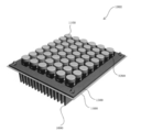
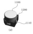
- FIG. 1 is a perspective view for explaining the overall outline of the electronic component mounting module 1000.
- the electronic component mounting module 1000 includes a first bus bar 1300, an insulating sheet 1400, and a second bus bar 1500 (not shown in FIG. 1), and a pedestal 1200 on the first bus bar 1300.
- a plurality of capacitors 1100 mounted on the surface are mounted on the surface.
- a heat sink 1600 is surface-mounted (surface contact) on the outer surface side of the second bus bar 1500.
- the bus bar laminated body can supply a large current and has excellent heat dissipation. Therefore, even if a large number of electronic components such as a capacitor 1100 are mounted at a high density, the electronic component It is possible to avoid thermal damage.
- the capacitor 1100 is known to be vulnerable to high heat, but the bus bar laminate of the present invention can maintain high reliability and high durability characteristics.
- Each of the bus bars 1300 and 1500 is made of a metal having a certain thickness in consideration of a large current and heat dissipation, and this makes it possible to obtain a considerably strong characteristic in terms of strength. Therefore, even a capacitor whose life is greatly affected by heat can be integrated without any problem.
- the first electrode soldering convex body 1510 provided in the second bus bar 1500 is disposed in the convex body opening 1310 of the first bus bar 1300, and the first bus bar 1500 is provided with the first bus bar 1500.
- the outer surface of the bus bar 1300 has substantially the same height as reflow soldering is possible.
- the first lead terminal 1110 and the second lead terminal 1120 are inserted into the pedestal 1200 and bent at the bottom thereof, and the pedestal 1200 is set on the capacitor 1100 so that it can be handled as a surface mount type electronic component.
- the first lead terminal 1110 is reflow soldered to the flat top of the first electrode soldering convex body 1510.
- the height of the top of the first electrode soldering convex body 1510 and the plane of the peripheral edge of the convex body opening 1310 of the first bus bar 1300 can be made uniform. This makes it possible to use reflow solder easily.
- the first electrode solder convex body 1510 has a desired clearance in the convex body opening 1310 provided in the first bus bar 1300 at a position corresponding to the first electrode solder convex body 1510. It arrange
- the second lead terminal 1120 of the electronic component that is surface-mounted at the peripheral edge of the convex body opening 1310 is fixed by reflow soldering on the upper surface side of the paper. That is, the surface mount type electronic component shown in the present embodiment is reflow soldered on the mounting side. More specifically, in the bus bar laminated body of FIG. 3, an electronic component is surface-mounted on the upper surface of the first bus bar 1300 on the upper surface side of the paper, and the upper surface of the first bus bar 1300 on the upper surface side of the paper is reflow soldered.
- the lead terminal of the electronic component is fixed by soldering. As described above, each lead terminal is not inserted into and fixed to the bus bar, but is bent at the bottom of the base, mounted in surface contact, and soldered.
- Each of the bus bars 1300 and 1500 is formed of a metal having a considerable thickness, and is excellent in thermal conductivity and allows a large current to flow with low resistance. Due to the smooth heat dissipation effect of the bus bar laminate, thermal damage of a plurality of electronic components mounted on the bus bar laminate can be prevented.
- a convex body opening 1310 having a larger diameter is provided in the first bus bar 1300 at a location corresponding to the first electrode solder convex body 1510 provided in the second bus bar 1500. It is done.
- the second lead terminal 1120 of the surface mount electronic component mounted on the outer surface side of the first bus bar 1300 is electrically and mechanically reflow soldered to the first bus bar 1300 at the periphery of the convex body opening 1310.
- the insulating sheet 1200 may be formed by applying various insulating films (for example, a polyimide film) or an insulating material such as a resist.
- the opening area corresponding to the first electrode solder convex body 1510 of 1400 can be made smaller than the opening area of the convex body opening 1310.
- the solder cannot contact the bus bar 1500, and the insulation characteristics can be ensured reliably and safely.
- a resist agent or the like is applied to the side wall (tapered in FIGS.
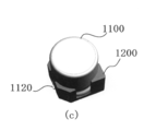
- FIGS. 4a, 4b, 4c, and 4d are diagrams illustrating a capacitor 1100 that is exemplified and mounted in the present embodiment configured as a surface mount type.
- a capacitor configuration is described as a typical example of an electronic component.
- the electronic component of the present invention is not limited to a capacitor, and may be any surface mount type electronic device. Good.
- the capacitor 1100 can be mounted by surface contact on the bottom surface of the pedestal 1200 by being fitted to the pedestal 1200 with the lead terminals 1110 and 1120 inserted therethrough.
- the first lead terminal 1110 and the second lead terminal 1120 are each inserted into the pedestal 1200 and bent along the bottom surface at the bottom surface, so that at least the tip portion protrudes from the edge of the pedestal 1200. . For this reason, when the capacitor 1100 and the pedestal 1200 are viewed from above, the front end portions of the first lead terminal 1110 and the second lead terminal 1120 are visible from the edge of the pedestal 1200.
- a pair of auxiliary terminals 1130 are provided on the bottom surface of the pedestal 1200 around the first lead terminal 1110 and the second lead terminal 1120, respectively. In the reflow soldering process, the first lead terminal 1110 and the second lead terminal 1120 are provided. By soldering each auxiliary terminal 1130 together with the two lead terminals 1120, the fixing strength is increased and the impact resistance and vibration resistance are improved.
- a part of the solder fillet for the first electrode 2110 is more preferably all formed in the flat top of the soldered convex body 1510 for the first electrode.
- the quality check and confirmation of the reflow soldering process can be carried out easily and quickly by observing and evaluating in plan view.
- the entire bottom surfaces of the first electrode 2110 and the second electrode 2120 are soldered, the mounting strength is increased, vibration resistance and impact resistance are improved, and thermal radiation characteristics are also improved. The reliability, durability, and life of the capacitor 2100 are improved.
- the external terminals of the surface mount component to be reflow soldered may be, for example, lead terminals exemplified in FIGS. 2a and 2b and electrode terminals exemplified in FIGS. 5a, 5b and 5c.
- the resin 1700 enters and fills the space around the first electrode soldering convex body 1510 and the convex body opening 1310.
- the overall strength is greatly increased, and vibration resistance, impact resistance and durability are improved.
- the capacitor 1100 is molded and integrated with the bus bars 1300 and 1500, so that the capacitor 1100 is fixed by the resin 1700, and the impact resistance is greatly improved.
- the bus bars 1300 and 1500 are not flat flat bus bars but have uneven shapes and increased surface areas, so that the contact area with the resin 1700 is increased.
- the heat dissipation characteristics and the adhesive strength can be increased. Even when large vibrations, impacts or accelerations are applied, the shape of the resin 1700 is maintained, so that the load on the lead terminals 1120 and 1110 is less than that when only the lead terminals 1120 and 1110 are fixed. That's it.
- the resin 1700 may be provided with an arbitrary path hole for venting the capacitor 1100.
- the resin 1700 may be molded with the heat sink 1600 provided.
- Capacitor 1110 .. First lead terminal, 1120 .. second lead terminal, 1130 .. Auxiliary terminal, 1200 ... pedestal, 1300 ... the first bus bar, 1310 .. Opening for convex body, 1400 .. Insulation sheet, 1500 ... second bus bar, 1510 .. Solder convex body for first electrode, 1600 ... Heat sink, 1700 .. Resin.
Landscapes
- Engineering & Computer Science (AREA)
- Power Engineering (AREA)
- Microelectronics & Electronic Packaging (AREA)
- Manufacturing & Machinery (AREA)
- Physics & Mathematics (AREA)
- Condensed Matter Physics & Semiconductors (AREA)
- General Physics & Mathematics (AREA)
- Computer Hardware Design (AREA)
- Chemical & Material Sciences (AREA)
- Materials Engineering (AREA)
- Fixed Capacitors And Capacitor Manufacturing Machines (AREA)
- Structures For Mounting Electric Components On Printed Circuit Boards (AREA)
- Electric Connection Of Electric Components To Printed Circuits (AREA)
- Structures Or Materials For Encapsulating Or Coating Semiconductor Devices Or Solid State Devices (AREA)
- Structure Of Printed Boards (AREA)
- Cooling Or The Like Of Semiconductors Or Solid State Devices (AREA)
Abstract
積層された陽極のバスバーと陰極のバスバーとで半田実装面の高さを揃えてリフロー半田を使用可能とした、バスバーを用いた表面実装タイプの電子部品モジュール等を提供することを目的とする。電子部品の外部端子を半田付けする領域をそれぞれ備える第一のバスバーと第二のバスバーとが絶縁して積層されるバスバー積層体であって、第一のバスバーは、開口部を備え、第二のバスバーは、第一のバスバー側に突出し、半田付けする領域である凸状体を備え、第二のバスバーの凸状体は開口部に対応する位置に配置され、第一のバスバーの半田付けする領域と凸状体の半田付けする領域とを、リフロー半田による電子部品の外部端子を半田付けが可能な程度に同一高さにしたバスバー積層体とする。
Description
本発明は、積層された陽極のバスバーと陰極のバスバーとで半田実装面の高さを揃えてリフロー半田を使用可能とした、バスバーを用いた表面実装タイプの電子部品モジュール等に関する。
複数の電子部品を搭載するモジュールにおいて大電流が印加される導電材料には金属板(バスバー)を用いることで抵抗が下がり、発熱を低減させると共に放熱性を向上させることができることが知られている。大電流を使用する場合には、小型の電子デバイスの実装に汎用されているいわゆるプリント配線基板等では放熱が追い付かず熱が蓄積されてしまうので、電子部品等が熱損傷を受ける懸念が生じる。
このため例えばコンデンサを複数個実装する場合には、陽極のバスバーと陰極のバスバーとを絶縁層(例えば絶縁シートや絶縁材の塗布層)を介して積層(貼り合わせ)し、当該貼り合わせたバスバーの一面に並べて複数個実装することで、放熱性を向上させる。
下記特許文献1の図4及び当該説明記載箇所には、「図4に示す第2の実施例のコンデンサモジュール31では、基板32が、絶縁シート33の両面に第1,第2の金属板34,35を貼り合わせた構造を有する。図6に、絶縁シート33を平面図で示す。絶縁シート33は、本実施例では、シリコーン樹脂からなり、0.1~0.05mm程度の厚みを有する。もっとも、絶縁シート33は、エポキシ樹脂(レジスト)などの他の合成樹脂を用いて構成されていてもよい。」と記載されている。
すなわち特許文献1では、第1の金属板34と第2の金属板35との間に絶縁シート33を挟んだ状態で貼り合わせ、積層コンデンサ3のリード端子3a,3bが、金属板に垂直に貫通立設され、リード端子3a,3bが金属板34,35と半田付けされる構造が開示されている。
特許文献1の図4に明示されているように、リード端子3aが上側の金属板34の底面に半田16で半田付けされて、リード端子3bが下側の金属板35の底面に半田17で半田付けされる。このため、このような構造では、ちょうど絶縁シート33及び下側の金属板35の厚さに相当する高さ分だけ、一対のリード端子3a,3bの半田付される高さが互いに相異なるものとなっている。この場合の半田付作業は、手作業により個々に半田付される場合には何ら問題は生じないが、フロー半田等を用いてある程度のスループットを期待して量産工程を考慮する場合にはこれに対応できない。
従来、積層した二枚のバスバーに複数の表面実装タイプまたはリード挿入タイプの電子部品を実装する際に、陽極のバスバーと陰極のバスバーとで実装面の高さ(すなわち、陽極と陰極の各リード端子の各バスバーへの半田付ポイントの高さ)が異なるため、リフロー半田等を使用することができず、電子部品の実装作業が煩雑になってしまう課題がある。
すなわち、従来のように一対のリード端子の半田付高さが互いに相異なるものとなる場合には、手作業によりそれぞれ半田付作業をすれば何ら問題はないが、量産工程などにおいて多用されるリフロー半田工程を利用しようとすれば、半田付ポイントの高さが異なる場合にはその工程遂行が困難となる。各バスバーは、大電流であればあるほど熱放散等を考慮してある程度の厚さを有するものであるが、リフロー半田工程にとって当該バスバー電極体の厚さに対応する半田付ポイントの高さの差異は無視できるものではない。
このため、陰極バスバーと陽極バスバーとを貼り合わせて用いた電子部品モジュールの各リード端子(表面実装タイプ)を、より量産効率の高いリフロー半田を利用して各バスバーに半田付できる構造が求められている。本発明は上述の問題点に鑑み為されたものであり、積層された陽極のバスバーと陰極のバスバーとで半田実装面の高さを揃えてリフロー半田を使用可能とした、バスバーを用いた表面実装タイプの電子部品モジュール等を提供することを目的とする。
本発明のバスバー積層体は、電子部品の外部端子を半田付けする領域をそれぞれ備える第一のバスバーと第二のバスバーとが絶縁して積層されるバスバー積層体であって、第一のバスバーは、開口部を備え、第二のバスバーは、第一のバスバー側に突出し、半田付けする領域である凸状体を備え、第二のバスバーの凸状体は開口部に対応する位置に配置され、第一のバスバーの半田付けする領域と凸状体の半田付けする領域とを、リフロー半田による電子部品の外部端子を半田付けが可能な程度に同一高さにしたことを特徴とする。
また、本発明の電子部品実装モジュールは、第一のバスバー側で外部端子が半田付された前記電子部品を備えることを特徴とする。
また、本発明の電子部品実装モジュールは、好ましくは第一リード端子の先端が、半田付凸状体の頭頂部内に配置されることを特徴とする。
また、本発明の電子部品実装モジュールは、さらに好ましくは半田付領域を含むバスバー積層体が樹脂モールドされたことを特徴とする。
また、本発明の電子部品実装モジュールは、さらに好ましくはバスバー積層体の、電子部品の実装側に対する裏面に、面一に接着されたヒートシンクを備えることを特徴とする。
また、本発明のバスバー積層体の製造方法は、絶縁積層された第一のバスバーと第二電子部品の外部端子を半田付けする領域をそれぞれ備える第一のバスバーと第二のバスバーとが絶縁して積層されるバスバー積層体の製造方法において、第一のバスバーに、開口部を形成する工程、並びに、第二のバスバーに、第一のバスバー側に突出し半田付けする領域である凸状体を形成する工程、を遂行した後、第二のバスバーの凸状体を開口部に対応する位置に配置し、第一のバスバーと第二のバスバーとを絶縁積層する工程を有し、第一のバスバーの半田付けする領域と凸状体の半田付けする領域とは、リフロー半田による電子部品の外部端子を半田付けが可能な程度に同一高さであるバスバー積層体の製造方法とする。
積層された陽極のバスバーと陰極のバスバーとで半田実装面の高さを揃えてリフロー半田を使用可能とした、バスバーを用いた表面実装タイプの電子部品モジュール等を提供できる。
本実施形態で例示するバスバー積層体は、大電流を利用する例えばコンデンサ等の複数の電子部品を、リフロー半田で平面状に並べて表面実装されて、車載用途等に利用されることができる。従来、バスバー積層体は、上層側のバスバーと下層側のバスバーとのそれぞれが相当程度の厚さを有していることから、実装される電子部品のリード端子が半田付される各バスバーの半田付ポイントに、高さ方向において当該厚さに相当する程度の相違が生じていた。
また、電子部品実装モジュールの技術トレンドは、小型・軽量化の進展とともに、実装される電子部品のチップ化がさらに進んでいる。仮に、実装する電子部品においてチップ部品とリード端子部品が混在するとなると、電気的・機械的に接続固定する半田付が二工程となるので工程が増えてコスト増大を招くため、いずれかに統一されることが好ましいことから、現在はコンデンサとコイルのチップ化が期待されているところである。
実施形態で提案する構成によれば、リフロー半田付後の必須工程である半田付品質確認の工程が容易となり、半田フィレットを画像処理または目視で確認することにより、半田付の品質を評価・確認することが可能となる。また、リフロー半田可能な程度の同一高さは、段差が0.6mm以下であることが好ましく、0.3mm以下とすることがさらに好ましいところ、本実施形態においては各バスバーへの半田付高さの差異をこのようなリフロー半田可能な程度以内に同一高さとすることができる。
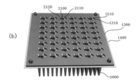
図1は、電子部品実装モジュール1000の全体概要を説明する斜視図である。図1に示すように、電子部品実装モジュール1000は、第一のバスバー1300と絶縁シート1400と第二のバスバー1500(図1では不図示)とを備え、第一のバスバー1300上には台座1200に装着された状態のコンデンサ1100が複数個表面実装されている。また、第二のバスバー1500の外面側には、ヒートシンク1600が面実装(面接触)されている。
図1に示すように、バスバー積層体は大電流の供給が可能であり、かつ放熱性にも優れているため、多数のコンデンサ1100等の電子部品を高密度で搭載しても、当該電子部品が熱損傷を受けることは回避可能である。特にコンデンサ1100は高熱に弱いことが知られているが、本発明のバスバー積層体においては高信頼性かつ高耐久性の特性を維持可能である。各バスバー1300,1500は、大電流及び放熱を考慮して一定程度の厚さを有する金属で構成されているが、これにより強度的にもかなり強い特性が得られるものとなっている。従って、熱によりその寿命が大きく左右されるコンデンサ等であっても問題なく集積可能となる。
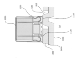
また、図2aはコンデンサ1100の中央で切断した場合の構成態様を説明する断面図であり、図2bはその拡大図である。図2aにおいて、第二のバスバー1500の外面側には面一に熱伝導フィルム1610とヒートシンク1600が貼付されており、これにより第二のバスバー1500の熱を効率的に外部へ放散することができる。第二のバスバー1500の外面側には、端子の突出や半田フィレット等の突起障害物が存在しないことから、熱伝導フィルム1610やヒートシンク1600を面一に大面積接触にて貼付することができるので、熱放散特性が向上する。なお、熱伝導フィルム1610は省略して直接ヒートシンク1600のみを設けてもよい。
また、図2bに示すように、第二のバスバー1500が備える第一電極用半田付凸状体1510は、第一のバスバー1300の凸状体用開口部1310内に配置されて、第一のバスバー1300の外面とはリフロー半田が可能な程度に略同一高さとされている。
そして、第一リード端子1110および第二リード端子1120は、台座1200に挿通されてその底面で曲折されており、コンデンサ1100に台座1200がセットせれることによって表面実装タイプの電子部品として取り扱い可能とされている。また、図2bから理解できるように、第一リード端子1110は第一電極用半田付凸状体1510の平らな頭頂部にリフロー半田付される。ここで、第一リード端子1110の少なくとも先端部は、台座1200から少し突出した状態で、第一電極用半田付凸状体1510の平らな頭頂部内からはみ出ることなく収まっているものとする。
これにより、上方から観察した場合に、第一リード端子1110の先端部が視認等(視認またはカメラ画像取得及びその処理)可能(視認またはカメラ画像取得及びその処理)となるので、その周りに形成される半田フィレットの状態観察によってリフロー半田の品質確認を行うことができる。また、第二リード端子1120の先端部は、台座1200から少し突出した状態で、第一のバスバー1300にリフロー半田付されている。
このような構成により、第一電極用半田付凸状体1510の頭頂部と、第一のバスバー1300の凸状体用開口部1310の周縁部の平面と、の相互の高さを揃えることが可能となり、リフロー半田の利用も容易となる。
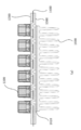
図3は、本実施形態のバスバー積層体の全体構成概要を説明する図である。図3において、バスバー積層体は、紙面上層側に記載されている第一のバスバー1300と、下層側に記載されている第二のバスバー1500と、第一のバスバー1300と第二のバスバー1500との間に配設された絶縁シート1400とを備える。第二のバスバー1500は、第一のバスバー1300側に突出した第一電極用半田付凸状体1510の平坦な頭頂部に、表面実装される電子部品の第一リード端子が、紙面上面側にリフロー半田固定される。また、第一電極用半田付凸状体1510は、第一電極用半田付凸状体1510に対応する位置に第一のバスバー1300に設けられた凸状体用開口部1310内に所望のクリアランスを設けて非接触となるように配置される。
また、第一のバスバー1300は、凸状体用開口部1310の周縁部において表面実装される電子部品の第二リード端子1120が、紙面上面側にリフロー半田固定される。すなわち、本実施形態で示す表面実装タイプの電子部品は、実装側においてリフロー半田付けされるものとする。より詳細には図3のバスバー積層体では、紙面上面側の第一のバスバー1300の上面に電子部品が表面実装されるものとなり、紙面上面側の第一のバスバー1300の上面でリフロー半田により当該電子部品のリード端子が半田付固定されるものとなる。各リード端子は、既に説明したようにバスバーに挿入固定されるものではなく、台座底面で曲折されて面接触で実装して半田付されるものである。
各バスバー1300,1500は相当程度の厚さを有する金属で形成されており、熱伝導性に優れるとともに大電流を低抵抗で流すことができるものである。バスバー積層体のスムースな放熱効果により、バスバー積層体に搭載される複数の電子部品の熱損傷を防止することができる。
図3から理解できるように、第二のバスバー1500が備える第一電極用半田付凸状体1510に対応する箇所に、より大きな口径の凸状体用開口部1310が第一のバスバー1300に設けられる。第一のバスバー1300の外面側に搭載された表面実装電子部品の第二リード端子1120は、凸状体用開口部1310の周辺部において第一のバスバー1300に電気的及び機械的にリフロー半田付固定される。なお、絶縁シート1200は、絶縁特性を有する各種フィルム(例えばポリイミドフィルム)やレジスト等の絶縁材の塗布によって形成してもよい。
なお、図3等において、第一のバスバー1300と第二のバスバー1500との間の、凸状体用開口部1310における絶縁特性をリフロー半田時等においてもより確実に維持するために、絶縁シート1400の第一電極用半田付凸状体1510に対応する開口面積を凸状体用開口部1310の開口面積より小さいものとすることができる。
また、絶縁シート1400の当該箇所の開口からは第一電極用半田付凸状体1510のみが露出されるものとして、その他の第二のバスバー1500の平面部位は露出されないようにするものとできる。これにより、仮にリフロー半田が過剰に凸状体用開口部1310辺縁部に付着してその内周壁を伝って第二のバスバー1500側に漏出したとしても、絶縁シート1400で阻止されて第二のバスバー1500に半田が接触することができないものとなり、絶縁特性を確実かつ安全に確保できるものとなる。さらに好ましくは、第一電極用半田付凸状体1510を形成する側壁(図2a,2bではテーパ状)や凸状体用開口部1310の側壁(図2a,2bでは垂直周壁)にレジスト剤等の絶縁材を配置・塗布等することにより、絶縁特性がさらに向上するものとなる。
また、図4a、4b、4c、4dは、表面実装タイプとして構成された本実施形態で例示実装されるコンデンサ1100を説明する図である。図4a、4b、4c、4dでは、電子部品の典型例としてコンデンサ構成を説明しているが、本発明の電子部品はコンデンサに限定されるものではなく、任意の表面実装タイプ電子デバイスであってよい。図4a、4b、4c、4dに示すように、コンデンサ1100は台座1200にリード端子1110,1120を挿通した状態で嵌装されていることにより、台座1200の底面で面接触により実装可能となる。
また、第一リード端子1110と第二リード端子1120とは、それぞれ台座1200に挿通されて底面で底面に沿って曲折されて、その少なくとも先端部分が台座1200の辺縁部から突出した状態となる。このため、コンデンサ1100及び台座1200を上方から平面視した場合には、台座1200のエッジから第一リード端子1110と第二リード端子1120の各先端部分が視認できる状態とされている。
また、台座1200の底面には、第一リード端子1110と第二リード端子1120とのそれぞれの周囲に一対の補助端子1130がそれぞれ設けられており、リフロー半田工程において、第一リード端子1110と第二リード端子1120と共に各補助端子1130も半田付されることにより、その固定強度が増大して耐衝撃性や耐振動性を向上させるものとなる。
また、図5a、5b、5cは、表面実装のチップタイプセラミックコンデンサ2100を実装した第二の本実施形態の電子部品実装モジュールを説明する概要図である。チップタイプセラミックコンデンサ2100は、第一電極2110と第二電極2120とを備えており、第一電極2110が第一電極用半田付凸状体1510の平坦な頭頂部内にリフロー半田付されるとともに、第二電極2120が第一のバスバー1300にリフロー半田付される。既に説明しているように、第一電極用半田付凸状体1510は、平板状の第二のバスバー1500の一部が凸形状とされたものであり、第二のバスバー1500の一部である。
このように形成することにより、第一電極2110に対する半田フィレットの一部が、より好ましくは全て、第一電極用半田付凸状体1510の平坦な頭頂部内に形成されることとなるので、上方からの平面視の観察・評価によって、リフロー半田工程の品質チェックと確認を容易に迅速に遂行できるものとなる。また、第一電極2110と第二電極2120との底面全体が半田付されることにより、実装強度が増大して耐振動性や耐衝撃性が向上するとともに熱放熱特性も向上することから、セラミックコンデンサ2100の信頼性や耐久性・寿命が向上するものとなる。ここで、リフロー半田付けされる表面実装部品の外部端子としては、例えば図2a,2bで例示したリード端子や図5a、5b、5cで例示する電極端子であってよい。
図6は、破線で示す樹脂1700でモールドされたコンデンサ実装モジュールの典型例を説明する図である。図6においては、第一のバスバー1300と第二のバスバー1500とコンデンサ1100の一部(典型的には台座を含む略下半分)を樹脂1700でモールドした状態を示している。なお、図6には明示していないが各リード端子1110,1120は既に半田付されているものである。
図6に示すように、樹脂1700でモールドすれば、当該樹脂1700が、第一電極用半田付凸状体1510の周囲空間や、凸状体用開口部1310内にも入り込んで充填されるので、放熱特性が向上するのみではなく、全体の強度も大きく増大するものとなり、耐振動性や耐衝撃性・耐久性が向上する。また、半田付に加えてコンデンサ1100が各バスバー1300,1500とモールド一体化されるので、コンデンサ1100が樹脂1700でも固定されるものとなって、耐衝撃性も大幅に向上するものとなる。
特に、図3及び図6から明らかなように、板状平面体の平坦なバスバーではなく凹凸形状を備えその表面積が増大したバスバー1300,1500とされているので、樹脂1700との接触面積を大きく確保できるものとなり、放熱特性や接着強度はこれにより増大するものとできる。大きな振動や衝撃・加速度が加わった場合でも、樹脂1700全体で形状保持するため、リード端子1120,1110のみで固定している場合に比べて、リード端子1120,1110への負荷の負担が小さくて済む。また、図示していないが、樹脂1700にはコンデンサ1100のガス抜きのための任意の経路孔を設けてもよい。また、ヒートシンク1600を設けた状態で、さらに樹脂1700でモールドするものとしてもよい。
本実施形態で例示する電子部品は、電子部品から突出したリード端子をバスバーの挿通孔に貫通させる必要はない。このため、電子部品を表面実装する場合において、電子部品とバスバーとの配向や相対的な向きを表面実装可能な範囲で自由に設計し変更することが可能である。従って、電子部品の実装における汎用性や自由度が向上するものとできる。
本発明のバスバー積層体や電子部品実装モジュール等は、上述の実施形態で説明した構成や方法に限定されるものではなく、当業者に自明な範囲でかつ本発明の技術思想の範囲内で適宜その構成を変更し、組み合わせ適用し、また方法を変更することができる。
本発明は、コンデンサを典型例とする複数の電子部品の実装モジュールに好適である。
1000・・電子部品実装モジュール、
1100・・コンデンサ、
1110・・第一リード端子、
1120・・第二リード端子、
1130・・補助端子、
1200・・台座、
1300・・第一のバスバー、
1310・・凸状体用開口部、
1400・・絶縁シート、
1500・・第二のバスバー、
1510・・第一電極用半田付凸状体、
1600・・ヒートシンク、
1700・・樹脂。
1100・・コンデンサ、
1110・・第一リード端子、
1120・・第二リード端子、
1130・・補助端子、
1200・・台座、
1300・・第一のバスバー、
1310・・凸状体用開口部、
1400・・絶縁シート、
1500・・第二のバスバー、
1510・・第一電極用半田付凸状体、
1600・・ヒートシンク、
1700・・樹脂。
Claims (6)
- 電子部品の外部端子を半田付けする領域をそれぞれ備える第一のバスバーと第二のバスバーとが絶縁して積層されるバスバー積層体であって、
前記第一のバスバーは、開口部を備え、
前記第二のバスバーは、前記第一のバスバー側に突出し、半田付けする領域である凸状体を備え、
前記第二のバスバーの前記凸状体は前記開口部に対応する位置に配置され、
前記第一のバスバーの半田付けする領域と前記凸状体の半田付けする領域とを、リフロー半田による前記電子部品の外部端子を半田付けが可能な程度に同一高さにしたことを特徴とするバスバー積層体。 - 請求項1に記載のバスバー積層体と、
前記第一のバスバー側で前記外部端子が半田付された前記電子部品を備えることを特徴とする電子部品実装モジュール。 - 請求項2に記載の電子部品実装モジュールにおいて、
前記外部端子の少なくとも先端が、前記凸状体の頭頂部内に配置されることを特徴とする電子部品実装モジュール。 - 請求項2または請求項3に記載の電子部品実装モジュールにおいて、
半田付領域を含む前記バスバー積層体が樹脂モールドされたことを特徴とする電子部品実装モジュール。 - 請求項2乃至請求項4のいずれか一項に記載の電子部品実装モジュールにおいて、
前記バスバー積層体の、前記電子部品の実装側に対する裏面に、面一に接着されたヒートシンクを備えることを特徴とする電子部品実装モジュール。 - 電子部品の外部端子を半田付けする領域をそれぞれ備える第一のバスバーと第二のバスバーとが絶縁して積層されるバスバー積層体の製造方法において、
前記第一のバスバーに、開口部を形成する工程、並びに、前記第二のバスバーに、前記第一のバスバー側に突出し半田付けする領域である凸状体を形成する工程、を遂行した後、
前記第二のバスバーの前記凸状体を前記開口部に対応する位置に配置し、前記第一のバスバーと前記第二のバスバーとを絶縁積層する工程を有し、
前記第一のバスバーの半田付けする領域と前記凸状体の半田付けする領域とは、リフロー半田による前記電子部品の外部端子を半田付けが可能な程度に同一高さであることを特徴とするバスバー積層体の製造方法。
Priority Applications (3)
| Application Number | Priority Date | Filing Date | Title |
|---|---|---|---|
| EP19814797.7A EP3822997A4 (en) | 2018-06-05 | 2019-05-18 | BUSBAR LAMINATE, MODULE FOR ASSEMBLING ELECTRONIC COMPONENTS THERETO, AND METHOD OF MAKING A BUSBAR LAMINATE |
| CN202311006806.7A CN117292944A (zh) | 2018-06-05 | 2019-05-18 | 汇流条层叠体、具备该汇流条层叠体的电子部件安装模块、以及汇流条层叠体的制造方法 |
| CN201980037845.9A CN112219249A (zh) | 2018-06-05 | 2019-05-18 | 汇流条层叠体、具备该汇流条层叠体的电子部件安装模块、以及汇流条层叠体的制造方法 |
Applications Claiming Priority (2)
| Application Number | Priority Date | Filing Date | Title |
|---|---|---|---|
| JP2018107427A JP2019212747A (ja) | 2018-06-05 | 2018-06-05 | バスバー積層体及びそれを備える電子部品実装モジュール、バスバー積層体の製造方法 |
| JP2018-107427 | 2018-06-05 |
Publications (1)
| Publication Number | Publication Date |
|---|---|
| WO2019235189A1 true WO2019235189A1 (ja) | 2019-12-12 |
Family
ID=68770252
Family Applications (1)
| Application Number | Title | Priority Date | Filing Date |
|---|---|---|---|
| PCT/JP2019/019816 WO2019235189A1 (ja) | 2018-06-05 | 2019-05-18 | バスバー積層体及びそれを備える電子部品実装モジュール、バスバー積層体の製造方法 |
Country Status (4)
| Country | Link |
|---|---|
| EP (1) | EP3822997A4 (ja) |
| JP (1) | JP2019212747A (ja) |
| CN (2) | CN112219249A (ja) |
| WO (1) | WO2019235189A1 (ja) |
Cited By (1)
| Publication number | Priority date | Publication date | Assignee | Title |
|---|---|---|---|---|
| EP4057785A1 (en) * | 2021-03-10 | 2022-09-14 | Rogers BV | Busbar and method for manufacturing a busbar |
Families Citing this family (1)
| Publication number | Priority date | Publication date | Assignee | Title |
|---|---|---|---|---|
| JP2023072794A (ja) * | 2021-11-15 | 2023-05-25 | 日本ケミコン株式会社 | バスバー積層体を備える電子部品実装モジュール及びその製造方法 |
Citations (5)
| Publication number | Priority date | Publication date | Assignee | Title |
|---|---|---|---|---|
| JPH0626117U (ja) * | 1992-08-31 | 1994-04-08 | 日本メクトロン株式会社 | 内部端子型積層母線 |
| JPH10340630A (ja) * | 1998-05-20 | 1998-12-22 | Furukawa Electric Co Ltd:The | 内部端子付きバスプレート積層体 |
| JP2001178151A (ja) | 1999-12-20 | 2001-06-29 | Murata Mfg Co Ltd | インバータ用コンデンサモジュール、インバータ及びコンデンサモジュール |
| JP2006005096A (ja) * | 2004-06-16 | 2006-01-05 | Auto Network Gijutsu Kenkyusho:Kk | 回路構成体 |
| JP2009259915A (ja) * | 2008-04-14 | 2009-11-05 | Mitsubishi Electric Corp | 制御基板およびその製造方法、電気機器 |
Family Cites Families (14)
| Publication number | Priority date | Publication date | Assignee | Title |
|---|---|---|---|---|
| JP2005056954A (ja) * | 2003-07-31 | 2005-03-03 | Elna Co Ltd | 回路基板組立体およびチップ型電子部品 |
| US20070165376A1 (en) * | 2006-01-17 | 2007-07-19 | Norbert Bones | Three phase inverter power stage and assembly |
| JP2007265945A (ja) * | 2006-03-30 | 2007-10-11 | Tokyo R & D Co Ltd | ラミネートセル集積型バッテリ及びバッテリモジュール |
| EP2043412B1 (de) * | 2007-09-28 | 2010-05-19 | Eberspächer Controls GmbH & Co. KG | Stromschiene mit Wärmeableitung |
| JP2010110170A (ja) * | 2008-10-31 | 2010-05-13 | Autonetworks Technologies Ltd | 回路構成体および電気接続箱 |
| TWI451817B (zh) * | 2011-05-26 | 2014-09-01 | 豐田自動織機股份有限公司 | 配線板及配線板的製造方法 |
| JP6044412B2 (ja) * | 2013-03-26 | 2016-12-14 | 株式会社オートネットワーク技術研究所 | リード端子と回路基板との接続構造、回路構成体及び電気接続箱 |
| JP6365186B2 (ja) * | 2014-09-29 | 2018-08-01 | 豊田合成株式会社 | バスバーモジュール |
| JP6274064B2 (ja) * | 2014-09-30 | 2018-02-07 | 豊田合成株式会社 | 電池モジュール |
| JP6467211B2 (ja) * | 2014-12-12 | 2019-02-06 | 日立オートモティブシステムズ株式会社 | 蓄電モジュール |
| JP6354600B2 (ja) * | 2015-01-16 | 2018-07-11 | 株式会社オートネットワーク技術研究所 | 回路構成体、電気接続箱及び回路構成体の製造方法 |
| CN105680266B (zh) * | 2016-04-11 | 2017-11-03 | 珠海英搏尔电气股份有限公司 | 交流电机控制器、叠层母排组件及其制作方法 |
| CN105845440B (zh) * | 2016-04-11 | 2017-09-01 | 珠海英搏尔电气股份有限公司 | 交流电机控制器、电容阵列及其制作方法 |
| CN206711772U (zh) * | 2017-04-27 | 2017-12-05 | 思源电气股份有限公司 | 一种超级电容模组结构 |
-
2018
- 2018-06-05 JP JP2018107427A patent/JP2019212747A/ja active Pending
-
2019
- 2019-05-18 EP EP19814797.7A patent/EP3822997A4/en active Pending
- 2019-05-18 CN CN201980037845.9A patent/CN112219249A/zh active Pending
- 2019-05-18 WO PCT/JP2019/019816 patent/WO2019235189A1/ja unknown
- 2019-05-18 CN CN202311006806.7A patent/CN117292944A/zh active Pending
Patent Citations (5)
| Publication number | Priority date | Publication date | Assignee | Title |
|---|---|---|---|---|
| JPH0626117U (ja) * | 1992-08-31 | 1994-04-08 | 日本メクトロン株式会社 | 内部端子型積層母線 |
| JPH10340630A (ja) * | 1998-05-20 | 1998-12-22 | Furukawa Electric Co Ltd:The | 内部端子付きバスプレート積層体 |
| JP2001178151A (ja) | 1999-12-20 | 2001-06-29 | Murata Mfg Co Ltd | インバータ用コンデンサモジュール、インバータ及びコンデンサモジュール |
| JP2006005096A (ja) * | 2004-06-16 | 2006-01-05 | Auto Network Gijutsu Kenkyusho:Kk | 回路構成体 |
| JP2009259915A (ja) * | 2008-04-14 | 2009-11-05 | Mitsubishi Electric Corp | 制御基板およびその製造方法、電気機器 |
Non-Patent Citations (1)
| Title |
|---|
| See also references of EP3822997A4 |
Cited By (1)
| Publication number | Priority date | Publication date | Assignee | Title |
|---|---|---|---|---|
| EP4057785A1 (en) * | 2021-03-10 | 2022-09-14 | Rogers BV | Busbar and method for manufacturing a busbar |
Also Published As
| Publication number | Publication date |
|---|---|
| JP2019212747A (ja) | 2019-12-12 |
| CN112219249A (zh) | 2021-01-12 |
| EP3822997A4 (en) | 2022-04-06 |
| CN117292944A (zh) | 2023-12-26 |
| EP3822997A1 (en) | 2021-05-19 |
Similar Documents
| Publication | Publication Date | Title |
|---|---|---|
| US10014111B2 (en) | Substrate terminal mounted electronic element | |
| KR20140027450A (ko) | 전자부품 | |
| JP5083226B2 (ja) | 半導体装置およびその製造方法 | |
| US20130223038A1 (en) | Module substrate and method for manufacturing module substrate | |
| TWI664881B (zh) | 零件模組 | |
| WO2019235189A1 (ja) | バスバー積層体及びそれを備える電子部品実装モジュール、バスバー積層体の製造方法 | |
| JP4854770B2 (ja) | プリント基板ユニット及び電子機器 | |
| JP7199639B2 (ja) | バスバー積層体及びそれを備える電子部品実装モジュール、バスバー積層体の製造方法 | |
| JP2015141904A (ja) | 電子回路モジュール及びその製造方法 | |
| JPH09266125A (ja) | 積層セラミック部品 | |
| TWI403231B (zh) | 表面黏著型電路板件模組及其製法 | |
| KR102409692B1 (ko) | 통신 모듈 | |
| WO2023085439A1 (ja) | バスバー積層体を備える電子部品実装モジュール及びその製造方法 | |
| JP2007103681A (ja) | 半導体装置およびその製造方法 | |
| CN113571484A (zh) | 功率模块用连接结构及其制备方法、功率模块 | |
| JP2006202870A (ja) | 立体的電子回路モジュールとその製造方法およびそれらを用いた電子装置 | |
| JP2002208767A (ja) | ハイブリッドic及びその製造方法並びに電池パック | |
| CN111902889B (zh) | 汇流条叠层板、该汇流条叠层板的电子元件安装模块及汇流条叠层板的制造方法 | |
| JP2002190565A (ja) | ハイブリッドic及びその製造方法 | |
| US20230395469A1 (en) | Thin semiconductor packaging unit | |
| JP7071707B2 (ja) | 電子部品実装モジュール及びその形成方法 | |
| JP2023136446A (ja) | 部品モジュール | |
| JP2020167311A (ja) | バスバー積層体及びそれを備える電子部品実装モジュール、電子部品実装モジュールの製造方法 | |
| JP3428083B2 (ja) | 半導体装置の製造方法 | |
| JP2006005035A (ja) | 電子部品収納用セラミックパッケージ集合体およびセラミックパッケージ |
Legal Events
| Date | Code | Title | Description |
|---|---|---|---|
| 121 | Ep: the epo has been informed by wipo that ep was designated in this application |
Ref document number: 19814797 Country of ref document: EP Kind code of ref document: A1 |
|
| NENP | Non-entry into the national phase |
Ref country code: DE |
|
| ENP | Entry into the national phase |
Ref document number: 2019814797 Country of ref document: EP Effective date: 20210111 |