WO2019229591A1 - 有機化合物、発光素子、発光装置、電子機器、および照明装置 - Google Patents
有機化合物、発光素子、発光装置、電子機器、および照明装置 Download PDFInfo
- Publication number
- WO2019229591A1 WO2019229591A1 PCT/IB2019/054218 IB2019054218W WO2019229591A1 WO 2019229591 A1 WO2019229591 A1 WO 2019229591A1 IB 2019054218 W IB2019054218 W IB 2019054218W WO 2019229591 A1 WO2019229591 A1 WO 2019229591A1
- Authority
- WO
- WIPO (PCT)
- Prior art keywords
- light
- emitting element
- layer
- light emitting
- abbreviation
- Prior art date
- Legal status (The legal status is an assumption and is not a legal conclusion. Google has not performed a legal analysis and makes no representation as to the accuracy of the status listed.)
- Ceased
Links
- 0 Cc1c(*)c2c(*)c3c(*=C)c(*)cc(*)c3c(*)c2c(*)c1* Chemical compound Cc1c(*)c2c(*)c3c(*=C)c(*)cc(*)c3c(*)c2c(*)c1* 0.000 description 4
- PYKZSDLUDVWQHQ-UHFFFAOYSA-N Bc1c(ccc2c3cc(cccc4)c4c2)c3ccc1 Chemical compound Bc1c(ccc2c3cc(cccc4)c4c2)c3ccc1 PYKZSDLUDVWQHQ-UHFFFAOYSA-N 0.000 description 1
- LMXOZFCNVIVYSH-UHFFFAOYSA-N Brc(cc1)cc2c1c(-c1cccc3ccccc13)c(cccc1)c1c2-c1c(cccc2)c2ccc1 Chemical compound Brc(cc1)cc2c1c(-c1cccc3ccccc13)c(cccc1)c1c2-c1c(cccc2)c2ccc1 LMXOZFCNVIVYSH-UHFFFAOYSA-N 0.000 description 1
- OAKPOEPOPWOKBG-UHFFFAOYSA-N C(C(C=CC=C1)C1=C1)c(cc2)c1c1c2c(-c(cc2)cc3c2c(-c2cccc4ccccc24)c(cccc2)c2c3-c2cccc3c2cccc3)ccc1 Chemical compound C(C(C=CC=C1)C1=C1)c(cc2)c1c1c2c(-c(cc2)cc3c2c(-c2cccc4ccccc24)c(cccc2)c2c3-c2cccc3c2cccc3)ccc1 OAKPOEPOPWOKBG-UHFFFAOYSA-N 0.000 description 1
- WFCMZNFRIRQQNT-UHFFFAOYSA-N Cc1cccc(N(C2=C(C=CC3=CC=C4N(c5cccc(C)c5)c5cc(C6(C(C=CC7C8C7)=C8C7=C6C=CC6C7C6)c6ccccc6)ccc5)C5=C3C4=CCC5CC2)c2cccc(C3(c4ccccc4C4C=CC=CC34)c3ccccc3)c2)c1 Chemical compound Cc1cccc(N(C2=C(C=CC3=CC=C4N(c5cccc(C)c5)c5cc(C6(C(C=CC7C8C7)=C8C7=C6C=CC6C7C6)c6ccccc6)ccc5)C5=C3C4=CCC5CC2)c2cccc(C3(c4ccccc4C4C=CC=CC34)c3ccccc3)c2)c1 WFCMZNFRIRQQNT-UHFFFAOYSA-N 0.000 description 1
Images






































Classifications
-
- C—CHEMISTRY; METALLURGY
- C07—ORGANIC CHEMISTRY
- C07C—ACYCLIC OR CARBOCYCLIC COMPOUNDS
- C07C15/00—Cyclic hydrocarbons containing only six-membered aromatic rings as cyclic parts
- C07C15/20—Polycyclic condensed hydrocarbons
- C07C15/38—Polycyclic condensed hydrocarbons containing four rings
-
- C—CHEMISTRY; METALLURGY
- C09—DYES; PAINTS; POLISHES; NATURAL RESINS; ADHESIVES; COMPOSITIONS NOT OTHERWISE PROVIDED FOR; APPLICATIONS OF MATERIALS NOT OTHERWISE PROVIDED FOR
- C09K—MATERIALS FOR MISCELLANEOUS APPLICATIONS, NOT PROVIDED FOR ELSEWHERE
- C09K11/00—Luminescent materials, e.g. electroluminescent or chemiluminescent
- C09K11/06—Luminescent materials, e.g. electroluminescent or chemiluminescent containing organic luminescent materials
-
- F—MECHANICAL ENGINEERING; LIGHTING; HEATING; WEAPONS; BLASTING
- F21—LIGHTING
- F21S—NON-PORTABLE LIGHTING DEVICES; SYSTEMS THEREOF; VEHICLE LIGHTING DEVICES SPECIALLY ADAPTED FOR VEHICLE EXTERIORS
- F21S2/00—Systems of lighting devices, not provided for in main groups F21S4/00 - F21S10/00 or F21S19/00, e.g. of modular construction
-
- H—ELECTRICITY
- H05—ELECTRIC TECHNIQUES NOT OTHERWISE PROVIDED FOR
- H05B—ELECTRIC HEATING; ELECTRIC LIGHT SOURCES NOT OTHERWISE PROVIDED FOR; CIRCUIT ARRANGEMENTS FOR ELECTRIC LIGHT SOURCES, IN GENERAL
- H05B33/00—Electroluminescent light sources
- H05B33/12—Light sources with substantially two-dimensional [2D] radiating surfaces
-
- H—ELECTRICITY
- H10—SEMICONDUCTOR DEVICES; ELECTRIC SOLID-STATE DEVICES NOT OTHERWISE PROVIDED FOR
- H10K—ORGANIC ELECTRIC SOLID-STATE DEVICES
- H10K50/00—Organic light-emitting devices
- H10K50/10—OLEDs or polymer light-emitting diodes [PLED]
- H10K50/11—OLEDs or polymer light-emitting diodes [PLED] characterised by the electroluminescent [EL] layers
- H10K50/12—OLEDs or polymer light-emitting diodes [PLED] characterised by the electroluminescent [EL] layers comprising dopants
-
- H—ELECTRICITY
- H10—SEMICONDUCTOR DEVICES; ELECTRIC SOLID-STATE DEVICES NOT OTHERWISE PROVIDED FOR
- H10K—ORGANIC ELECTRIC SOLID-STATE DEVICES
- H10K85/00—Organic materials used in the body or electrodes of devices covered by this subclass
- H10K85/60—Organic compounds having low molecular weight
- H10K85/615—Polycyclic condensed aromatic hydrocarbons, e.g. anthracene
-
- H—ELECTRICITY
- H10—SEMICONDUCTOR DEVICES; ELECTRIC SOLID-STATE DEVICES NOT OTHERWISE PROVIDED FOR
- H10K—ORGANIC ELECTRIC SOLID-STATE DEVICES
- H10K85/00—Organic materials used in the body or electrodes of devices covered by this subclass
- H10K85/60—Organic compounds having low molecular weight
- H10K85/615—Polycyclic condensed aromatic hydrocarbons, e.g. anthracene
- H10K85/622—Polycyclic condensed aromatic hydrocarbons, e.g. anthracene containing four rings, e.g. pyrene
-
- H—ELECTRICITY
- H10—SEMICONDUCTOR DEVICES; ELECTRIC SOLID-STATE DEVICES NOT OTHERWISE PROVIDED FOR
- H10K—ORGANIC ELECTRIC SOLID-STATE DEVICES
- H10K85/00—Organic materials used in the body or electrodes of devices covered by this subclass
- H10K85/60—Organic compounds having low molecular weight
- H10K85/615—Polycyclic condensed aromatic hydrocarbons, e.g. anthracene
- H10K85/626—Polycyclic condensed aromatic hydrocarbons, e.g. anthracene containing more than one polycyclic condensed aromatic rings, e.g. bis-anthracene
-
- C—CHEMISTRY; METALLURGY
- C07—ORGANIC CHEMISTRY
- C07C—ACYCLIC OR CARBOCYCLIC COMPOUNDS
- C07C2601/00—Systems containing only non-condensed rings
- C07C2601/02—Systems containing only non-condensed rings with a three-membered ring
-
- C—CHEMISTRY; METALLURGY
- C07—ORGANIC CHEMISTRY
- C07C—ACYCLIC OR CARBOCYCLIC COMPOUNDS
- C07C2601/00—Systems containing only non-condensed rings
- C07C2601/18—Systems containing only non-condensed rings with a ring being at least seven-membered
-
- C—CHEMISTRY; METALLURGY
- C07—ORGANIC CHEMISTRY
- C07C—ACYCLIC OR CARBOCYCLIC COMPOUNDS
- C07C2603/00—Systems containing at least three condensed rings
- C07C2603/02—Ortho- or ortho- and peri-condensed systems
- C07C2603/04—Ortho- or ortho- and peri-condensed systems containing three rings
- C07C2603/06—Ortho- or ortho- and peri-condensed systems containing three rings containing at least one ring with less than six ring members
- C07C2603/10—Ortho- or ortho- and peri-condensed systems containing three rings containing at least one ring with less than six ring members containing five-membered rings
- C07C2603/12—Ortho- or ortho- and peri-condensed systems containing three rings containing at least one ring with less than six ring members containing five-membered rings only one five-membered ring
- C07C2603/18—Fluorenes; Hydrogenated fluorenes
-
- C—CHEMISTRY; METALLURGY
- C07—ORGANIC CHEMISTRY
- C07C—ACYCLIC OR CARBOCYCLIC COMPOUNDS
- C07C2603/00—Systems containing at least three condensed rings
- C07C2603/02—Ortho- or ortho- and peri-condensed systems
- C07C2603/04—Ortho- or ortho- and peri-condensed systems containing three rings
- C07C2603/22—Ortho- or ortho- and peri-condensed systems containing three rings containing only six-membered rings
- C07C2603/24—Anthracenes; Hydrogenated anthracenes
-
- C—CHEMISTRY; METALLURGY
- C07—ORGANIC CHEMISTRY
- C07C—ACYCLIC OR CARBOCYCLIC COMPOUNDS
- C07C2603/00—Systems containing at least three condensed rings
- C07C2603/02—Ortho- or ortho- and peri-condensed systems
- C07C2603/40—Ortho- or ortho- and peri-condensed systems containing four condensed rings
- C07C2603/42—Ortho- or ortho- and peri-condensed systems containing four condensed rings containing only six-membered rings
-
- C—CHEMISTRY; METALLURGY
- C07—ORGANIC CHEMISTRY
- C07C—ACYCLIC OR CARBOCYCLIC COMPOUNDS
- C07C2603/00—Systems containing at least three condensed rings
- C07C2603/02—Ortho- or ortho- and peri-condensed systems
- C07C2603/40—Ortho- or ortho- and peri-condensed systems containing four condensed rings
- C07C2603/42—Ortho- or ortho- and peri-condensed systems containing four condensed rings containing only six-membered rings
- C07C2603/44—Naphthacenes; Hydrogenated naphthacenes
-
- C—CHEMISTRY; METALLURGY
- C07—ORGANIC CHEMISTRY
- C07C—ACYCLIC OR CARBOCYCLIC COMPOUNDS
- C07C2603/00—Systems containing at least three condensed rings
- C07C2603/93—Spiro compounds
- C07C2603/94—Spiro compounds containing "free" spiro atoms
-
- C—CHEMISTRY; METALLURGY
- C09—DYES; PAINTS; POLISHES; NATURAL RESINS; ADHESIVES; COMPOSITIONS NOT OTHERWISE PROVIDED FOR; APPLICATIONS OF MATERIALS NOT OTHERWISE PROVIDED FOR
- C09K—MATERIALS FOR MISCELLANEOUS APPLICATIONS, NOT PROVIDED FOR ELSEWHERE
- C09K2211/00—Chemical nature of organic luminescent or tenebrescent compounds
- C09K2211/10—Non-macromolecular compounds
- C09K2211/1003—Carbocyclic compounds
- C09K2211/1011—Condensed systems
-
- H—ELECTRICITY
- H10—SEMICONDUCTOR DEVICES; ELECTRIC SOLID-STATE DEVICES NOT OTHERWISE PROVIDED FOR
- H10K—ORGANIC ELECTRIC SOLID-STATE DEVICES
- H10K2101/00—Properties of the organic materials covered by group H10K85/00
- H10K2101/10—Triplet emission
-
- H—ELECTRICITY
- H10—SEMICONDUCTOR DEVICES; ELECTRIC SOLID-STATE DEVICES NOT OTHERWISE PROVIDED FOR
- H10K—ORGANIC ELECTRIC SOLID-STATE DEVICES
- H10K2101/00—Properties of the organic materials covered by group H10K85/00
- H10K2101/20—Delayed fluorescence emission
-
- H—ELECTRICITY
- H10—SEMICONDUCTOR DEVICES; ELECTRIC SOLID-STATE DEVICES NOT OTHERWISE PROVIDED FOR
- H10K—ORGANIC ELECTRIC SOLID-STATE DEVICES
- H10K50/00—Organic light-emitting devices
- H10K50/10—OLEDs or polymer light-emitting diodes [PLED]
- H10K50/11—OLEDs or polymer light-emitting diodes [PLED] characterised by the electroluminescent [EL] layers
-
- H—ELECTRICITY
- H10—SEMICONDUCTOR DEVICES; ELECTRIC SOLID-STATE DEVICES NOT OTHERWISE PROVIDED FOR
- H10K—ORGANIC ELECTRIC SOLID-STATE DEVICES
- H10K50/00—Organic light-emitting devices
- H10K50/10—OLEDs or polymer light-emitting diodes [PLED]
- H10K50/11—OLEDs or polymer light-emitting diodes [PLED] characterised by the electroluminescent [EL] layers
- H10K50/125—OLEDs or polymer light-emitting diodes [PLED] characterised by the electroluminescent [EL] layers specially adapted for multicolour light emission, e.g. for emitting white light
- H10K50/13—OLEDs or polymer light-emitting diodes [PLED] characterised by the electroluminescent [EL] layers specially adapted for multicolour light emission, e.g. for emitting white light comprising stacked EL layers within one EL unit
-
- H—ELECTRICITY
- H10—SEMICONDUCTOR DEVICES; ELECTRIC SOLID-STATE DEVICES NOT OTHERWISE PROVIDED FOR
- H10K—ORGANIC ELECTRIC SOLID-STATE DEVICES
- H10K59/00—Integrated devices, or assemblies of multiple devices, comprising at least one organic light-emitting element covered by group H10K50/00
- H10K59/10—OLED displays
- H10K59/12—Active-matrix OLED [AMOLED] displays
-
- H—ELECTRICITY
- H10—SEMICONDUCTOR DEVICES; ELECTRIC SOLID-STATE DEVICES NOT OTHERWISE PROVIDED FOR
- H10K—ORGANIC ELECTRIC SOLID-STATE DEVICES
- H10K59/00—Integrated devices, or assemblies of multiple devices, comprising at least one organic light-emitting element covered by group H10K50/00
- H10K59/30—Devices specially adapted for multicolour light emission
- H10K59/38—Devices specially adapted for multicolour light emission comprising colour filters or colour changing media [CCM]
-
- H—ELECTRICITY
- H10—SEMICONDUCTOR DEVICES; ELECTRIC SOLID-STATE DEVICES NOT OTHERWISE PROVIDED FOR
- H10K—ORGANIC ELECTRIC SOLID-STATE DEVICES
- H10K59/00—Integrated devices, or assemblies of multiple devices, comprising at least one organic light-emitting element covered by group H10K50/00
- H10K59/40—OLEDs integrated with touch screens
Definitions
- One embodiment of the present invention relates to a novel organic compound.
- the present invention relates to an organic compound having a benzo [a] anthracene skeleton and an anthracene skeleton.
- the present invention relates to a light-emitting element, a light-emitting device, an electronic device, and a lighting device including the organic compound.
- one embodiment of the present invention is not limited to the above technical field.
- One embodiment of the present invention relates to an object, a method, or a manufacturing method.
- one embodiment of the present invention relates to an organic compound, a light-emitting element, a light-emitting device, a lighting device, and manufacturing methods thereof.
- Another embodiment of the present invention relates to a novel method for synthesizing an organic compound having a benzo [a] anthracene skeleton and an anthracene skeleton.
- a method for manufacturing a light-emitting element, a light-emitting device, a display device, an electronic device, and a lighting device including the organic compound can be given as an example. it can.
- a light-emitting element (organic EL element) using electroluminescence (EL) using an organic compound has been put into practical use.
- the basic structure of these light-emitting elements is such that an organic compound layer (EL layer) containing a light-emitting material is sandwiched between a pair of electrodes.
- Light emission from the light-emitting material can be obtained by applying a voltage to this element, injecting carriers, and utilizing the recombination energy of the carriers.
- Such a light-emitting element is a self-luminous type, when used for a display pixel, there are advantages such as high visibility and no need for a backlight, and it is suitable as a flat panel display element.
- a display using such a light emitting element has a great advantage that it can be manufactured to be thin and light. Another feature is that the response speed is very fast.
- these light emitting elements can continuously form a light emitting layer in two dimensions, light emission can be obtained in a planar shape. This is a feature that is difficult to obtain with a point light source typified by an incandescent bulb or LED, or a line light source typified by a fluorescent lamp.
- a point light source typified by an incandescent bulb or LED
- a line light source typified by a fluorescent lamp.
- light emitted from an organic compound can be emitted without containing ultraviolet light by selecting a material, the utility value as a surface light source applicable to illumination or the like is also high.
- a method using triplet excitons can be used to increase the efficiency of the fluorescent light emitting device.
- highly efficient fluorescent light-emitting devices using triplet-triplet annihilation (TTA) have been reported.
- the material used for the light-emitting element is required to have good light emission efficiency and reliability.
- a method using TTA can be used to increase the efficiency of the fluorescent light emitting device.
- TTA it is necessary to convert triplet excitons generated in the light emitting layer into singlet excitons. Therefore, a material that can efficiently convert triplet excitons to singlet excitons is required.
- One embodiment of the present invention is an organic compound having a substituted or unsubstituted benzo [a] anthracene skeleton and a substituted or unsubstituted anthracene skeleton, and the benzo [a] anthracene skeleton is bonded to the 2-position of the anthracene skeleton. is there.
- Another embodiment of the present invention is an organic compound represented by General Formula (G1) below.
- any one of R 1 to R 12 is a substituent represented by the following formula (g1), each other R 1 through R 12 independently represent hydrogen, carbon atoms 1 It represents any one of an alkyl group having 6 to 6 carbon atoms, a cycloalkyl group having 3 to 6 carbon atoms, and a substituted or unsubstituted aryl group having 6 to 13 carbon atoms forming a ring.
- R 21 to R 29 each independently represent hydrogen, an alkyl group having 1 to 6 carbon atoms, a cycloalkyl group having 3 to 6 carbon atoms, or 6 to 13 carbon atoms forming a ring. Represents any one of substituted or unsubstituted aryl groups.
- Another embodiment of the present invention is an organic compound represented by General Formula (G2) below.
- R 1 to R 3 , R 5 to R 12, and R 21 to R 29 are each independently hydrogen, an alkyl group having 1 to 6 carbon atoms, a cycloalkyl group having 3 to 6 carbon atoms, or , Represents any one of a substituted or unsubstituted aryl group having 6 to 13 carbon atoms forming a ring.
- the skeletons are bonded to each other at the 2-position of the anthracene skeleton and the 4-position of the benzo [a] anthracene skeleton. With this configuration, an organic compound with favorable reliability can be obtained.
- Another embodiment of the present invention is an organic compound represented by General Formula (G3) below.
- R 24 and R 29 are each independently preferably a substituted or unsubstituted aryl group having 6 to 13 carbon atoms, and more preferably a substituted or unsubstituted aryl group.
- R 24 is preferably a substituted or unsubstituted phenyl group
- R 29 is preferably a substituted or unsubstituted naphthyl group.
- Another embodiment of the present invention is an organic compound represented by any one of the following structural formulas (100) to (104), (115), (120), (167), and (117).
- Another embodiment of the present invention is a light-emitting element which includes an EL layer between a pair of electrodes and includes the organic compound described in any of the above structures in the EL layer.
- the organic compound is preferably contained in the light emitting layer in the EL layer.
- the light-emitting element in each of the above structures has an EL layer between an anode and a cathode.
- the EL layer preferably includes at least a light emitting layer.
- the EL layer may include a hole injection layer, a hole transport layer, an electron transport layer, an electron injection layer, and other functional layers.
- Another embodiment of the present invention is a display device including the light-emitting element having any of the above structures and at least one of a color filter or a transistor.
- Another embodiment of the present invention is an electronic device including the display device and at least one of a housing and a touch sensor.
- Another embodiment of the present invention is a lighting device including the light-emitting element having any of the above structures and at least one of a housing and a touch sensor.
- One embodiment of the present invention includes not only a light-emitting device including a light-emitting element but also an electronic device including the light-emitting device. Therefore, a light-emitting device in this specification refers to an image display device or a light source (including a lighting device).
- a display module in which a connector such as an FPC (Flexible Printed Circuit) or TCP (Tape Carrier Package) is attached to the light emitting element a display module in which a printed wiring board is provided at the end of the TCP, or a COG (Chip On) in the light emitting element.
- a display module in which an IC (integrated circuit) is directly mounted by a glass method is also an embodiment of the present invention.
- a novel organic compound can be provided.
- a novel organic compound having a benzo [a] anthracene skeleton can be provided.
- a light-emitting element with favorable emission efficiency can be provided.
- a light-emitting element with favorable lifetime can be provided.
- a light-emitting element with favorable color purity can be provided.
- a light-emitting element with low driving voltage can be provided.
- a light-emitting element with a high delayed fluorescence ratio can be provided.
- a highly reliable light-emitting element, light-emitting device, and electronic device can be provided.
- a light-emitting element, a light-emitting device, and an electronic device with low power consumption can be provided.
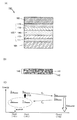
- FIGS. 3A and 3B are schematic views of a light-emitting element according to one embodiment of the present invention.
- FIGS. FIG. 5C is a graph illustrating the energy level correlation of the light-emitting element of one embodiment of the present invention.
- FIGS. 3A and 3B are schematic views of a light-emitting element according to one embodiment of the present invention.
- FIGS. FIG. 5C is a graph illustrating the energy level correlation of the light-emitting element of one embodiment of the present invention.
- 1 is a schematic diagram of a light-emitting element according to one embodiment of the present invention.
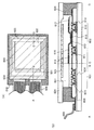
- FIGS. 4A and 4B are conceptual diagrams of an active matrix light-emitting device according to one embodiment of the present invention.
- FIGS. 4A and 4B are conceptual diagrams of an active matrix light-emitting device according to one embodiment of the present invention.
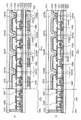
- FIGS. 1 is a conceptual diagram of an active matrix light-emitting device according to one embodiment of the present invention.
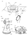
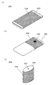
- FIGS. 6A to 6D each illustrate an electronic device according to one embodiment of the present invention.
- FIGS. FIGS. 6A to 6E each illustrate an electronic device according to one embodiment of the present invention.
- FIGS. FIGS. 7A to 7C each illustrate an electronic device according to one embodiment of the present invention.
- FIGS. FIGS. 6A and 6B each illustrate an electronic device according to one embodiment of the present invention.
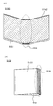
- FIGS. FIGS. 4A to 4C each illustrate a lighting device according to one embodiment of the present invention.
- FIG. 10 illustrates a lighting device according to one embodiment of the present invention.
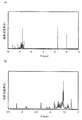
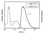
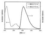
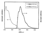
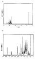
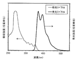
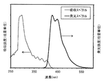
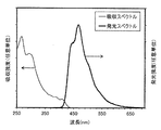
- A (B) The figure explaining the NMR chart of the compound based on an Example. The figure explaining the absorption spectrum and emission spectrum of a compound based on an Example. The figure explaining the absorption spectrum and emission spectrum of a compound based on an Example.
- A) (B) The figure explaining the NMR chart of the compound based on an Example. The figure explaining the absorption spectrum and emission spectrum of a compound based on an Example.
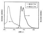
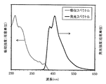
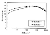
- the figure explaining the absorption spectrum and emission spectrum of a compound based on an Example. (A) (B) The figure explaining the NMR chart of the compound based on an Example. The figure explaining the absorption spectrum and emission spectrum of a compound based on an Example. The figure explaining the absorption spectrum and emission spectrum of a compound based on an Example. (A) (B) The figure explaining the NMR chart of the compound based on an Example. The figure explaining the absorption spectrum and emission spectrum of a compound based on an Example. The figure explaining the absorption spectrum and emission spectrum of a compound based on an Example. 6A and 6B illustrate current efficiency-luminance characteristics of a light-emitting element according to an example.
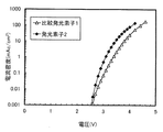
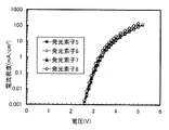
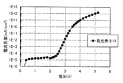
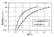
- 6A and 6B illustrate current density-voltage characteristics of a light-emitting element according to an example.
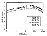
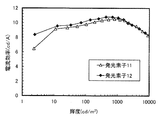
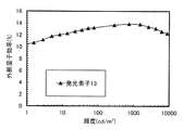
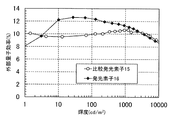
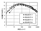
- 6A and 6B illustrate an external quantum efficiency-luminance characteristic of a light-emitting element according to an example.
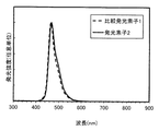
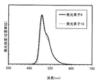
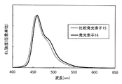
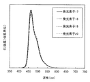
- 6A and 6B illustrate an emission spectrum of a light-emitting element according to an example.
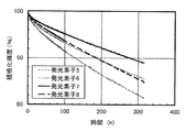
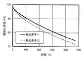
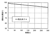
- 6A and 6B illustrate a result of a reliability test of a light-emitting element according to an example.
- 6A and 6B illustrate current efficiency-luminance characteristics of a light-emitting element according to an example.
- 6A and 6B illustrate current density-voltage characteristics of a light-emitting element according to an example.
- 6A and 6B illustrate an external quantum efficiency-luminance characteristic of a light-emitting element according to an example.
- 6A and 6B illustrate an emission spectrum of a light-emitting element according to an example.
- 6A and 6B illustrate a result of a reliability test of a light-emitting element according to an example.
- 6A and 6B illustrate current efficiency-luminance characteristics of a light-emitting element according to an example.
- 6A and 6B illustrate current density-voltage characteristics of a light-emitting element according to an example.
- 6A and 6B illustrate an external quantum efficiency-luminance characteristic of a light-emitting element according to an example.
- 6A and 6B illustrate an emission spectrum of a light-emitting element according to an example.
- 6A and 6B illustrate a result of a reliability test of a light-emitting element according to an example.
- 6A and 6B illustrate current efficiency-luminance characteristics of a light-emitting element according to an example.
- 6A and 6B illustrate current density-voltage characteristics of a light-emitting element according to an example.
- 6A and 6B illustrate an external quantum efficiency-luminance characteristic of a light-emitting element according to an example.
- 6A and 6B illustrate an emission spectrum of a light-emitting element according to an example.
- 6A and 6B illustrate a result of a reliability test of a light-emitting element according to an example.
- 6A and 6B illustrate current efficiency-luminance characteristics of a light-emitting element according to an example.
- 6A and 6B illustrate current density-voltage characteristics of a light-emitting element according to an example.
- 6A and 6B illustrate an external quantum efficiency-luminance characteristic of a light-emitting element according to an example.
- 6A and 6B illustrate an emission spectrum of a light-emitting element according to an example.
- 6A and 6B illustrate a result of a reliability test of a light-emitting element according to an example.
- 6A and 6B illustrate current efficiency-luminance characteristics of a light-emitting element according to an example.
- 6A and 6B illustrate current density-voltage characteristics of a light-emitting element according to an example.
- 6A and 6B illustrate an external quantum efficiency-luminance characteristic of a light-emitting element according to an example.
- 6A and 6B illustrate an emission spectrum of a light-emitting element according to an example.
- 6A and 6B illustrate current efficiency-luminance characteristics of a light-emitting element according to an example.
- 6A and 6B illustrate current density-voltage characteristics of a light-emitting element according to an example.
- 6A and 6B illustrate an external quantum efficiency-luminance characteristic of a light-emitting element according to an example.
- 6A and 6B illustrate an emission spectrum of a light-emitting element according to an example.
- 6A and 6B illustrate a result of a reliability test of a light-emitting element according to an example.
- 6A and 6B illustrate current efficiency-luminance characteristics of a light-emitting element according to an example.
- 6A and 6B illustrate current density-voltage characteristics of a light-emitting element according to an example.
- 6A and 6B illustrate an external quantum efficiency-luminance characteristic of a light-emitting element according to an example.
- 6A and 6B illustrate an emission spectrum of a light-emitting element according to an example.
- (A) (B) The figure explaining the result of the reliability test of the light emitting element based on an Example.
- (A) (B) The figure explaining the NMR chart of the compound based on an Example.
- the figure explaining the absorption spectrum and emission spectrum of a compound based on an Example The figure explaining the absorption spectrum and emission spectrum of a compound based on an Example.
- (A) (B) The figure explaining the NMR chart of the compound based on an Example.
- the figure explaining the absorption spectrum and emission spectrum of a compound based on an Example The figure explaining the absorption spectrum and emission spectrum of a compound based on an Example.
- the figure explaining the absorption spectrum and emission spectrum of a compound based on an Example The figure explaining the absorption spectrum and emission spectrum of a compound based on an Example.
- the figure explaining the absorption spectrum and emission spectrum of a compound based on an Example The figure explaining the absorption spectrum and emission spectrum of a compound based on an Example.
- 6A and 6B illustrate current efficiency-luminance characteristics of a light-emitting element according to an example.
- 6A and 6B illustrate current density-voltage characteristics of a light-emitting element according to an example.
- 6A and 6B illustrate an external quantum efficiency-luminance characteristic of a light-emitting element according to an example.
- 6A and 6B illustrate an emission spectrum of a light-emitting element according to an example.
- 6A and 6B illustrate a result of a reliability test of a light-emitting element according to an example.
- 6A and 6B illustrate a result of a reliability test of a light-emitting element according to an example.
- each component is not necessarily limited to the size, and is not limited to the relative size between the components.
- the ordinal numbers attached as the first, second, third, etc. are used for the sake of convenience and do not indicate the order of steps or the positional relationship between the upper and lower sides. Therefore, for example, the description can be made by appropriately replacing “first” with “second” or “third”.
- the ordinal numbers described in this specification and the like may not match the ordinal numbers used to specify one embodiment of the present invention.
- film and “layer” can be interchanged with each other depending on the case or circumstances.
- conductive layer may be changed to the term “conductive film”.
- insulating film may be changed to the term “insulating layer” in some cases.
- the organic compound of one embodiment of the present invention is an organic compound represented by the following general formula (G1).
- any one of R 1 to R 12 is a substituent represented by the following formula (g1), each other R 1 through R 12 independently represent hydrogen, carbon atoms 1 It represents any one of an alkyl group having 6 to 6 carbon atoms, a cycloalkyl group having 3 to 6 carbon atoms, and a substituted or unsubstituted aryl group having 6 to 13 carbon atoms forming a ring.
- R 21 to R 29 each independently represent hydrogen, an alkyl group having 1 to 6 carbon atoms, a cycloalkyl group having 3 to 6 carbon atoms, or 6 to 13 carbon atoms forming a ring. Represents any one of substituted or unsubstituted aryl groups.
- the organic compound according to one embodiment of the present invention has a substituted or unsubstituted benzo [a] anthracene skeleton and a substituted or unsubstituted anthracene skeleton, and the benzo [a] anthracene skeleton is bonded at the 2-position of the anthracene skeleton It is an organic compound.
- a light-emitting element with favorable emission efficiency and / or reliability can be obtained.
- the ratio of the delayed fluorescent component in the total light-emitting component (initial light-emitting component + delayed fluorescent component) can be obtained. That is, since TTA, which will be described later, can be used efficiently, a light-emitting element with high light emission efficiency can be obtained.
- an organic compound having a benzo [a] anthracene skeleton at the 2-position of the anthracene skeleton has a large ⁇ -conjugated system, the electron transporting property is favorable. Therefore, a light-emitting element with low driving voltage can be manufactured by using the organic compound which is one embodiment of the present invention for the light-emitting layer and / or the electron-transport layer of the EL layer.
- the organic compound of one embodiment of the present invention is an organic compound represented by the following general formula (G2).
- R 1 to R 3 , R 5 to R 12, and R 21 to R 29 are each independently hydrogen, an alkyl group having 1 to 6 carbon atoms, a cycloalkyl group having 3 to 6 carbon atoms, or , Represents any one of a substituted or unsubstituted aryl group having 6 to 13 carbon atoms forming a ring.
- the conjugated system is difficult to spread between the anthracene skeleton and the benzo [a] anthracene skeleton. It can be a compound. Therefore, it can be suitably used for a blue fluorescent element. Further, with this structure, an organic compound with favorable reliability can be obtained. Moreover, TTA can be used efficiently.
- an organic compound with favorable reliability can be obtained by directly bonding an electrochemically stable anthracene skeleton and a benzo [a] anthracene skeleton.
- the organic compound of one embodiment of the present invention is an organic compound represented by the following general formula (G3).
- R 21 to R 29 each independently represent hydrogen, an alkyl group having 1 to 6 carbon atoms, a cycloalkyl group having 3 to 6 carbon atoms, or a carbon number having 6 to 13 carbon atoms forming a ring. It represents either one of a substituted or unsubstituted aryl group.
- the benzo [a] anthracene skeleton has no substituent because it is electrochemically stable and has good reliability. Moreover, since synthesis is easy, it is preferable.
- R 24 and R 29 are each independently preferably a substituted or unsubstituted aryl group having 6 to 13 carbon atoms.
- R 24 and R 29 are each independently preferably a substituted or unsubstituted aryl group having 6 to 13 carbon atoms.
- R 24 and R 29 are preferably each independently a substituted or unsubstituted phenyl group or a substituted or unsubstituted naphthyl group. It is preferable to use a bulky aryl group such as a naphthyl group because heat resistance is improved. More preferably, R 24 is a substituted or unsubstituted phenyl group, and R 29 is a substituted or unsubstituted naphthyl group. By introducing different aryl groups into R 24 and R 29 , a light-emitting element with good heat resistance and good reliability can be obtained.
- R 1 to R 12 and R 21 to R 29 are, for example, hydrogen, an alkyl group having 1 to 6 carbon atoms, a substituted or unsubstituted carbon number of 3 to 6 cycloalkyl group or an aryl group having 6 to 13 carbon atoms constituting a substituted or unsubstituted ring.
- the alkyl group include a methyl group, an ethyl group, a propyl group, an isopropyl group, a butyl group, an isobutyl group, a tert-butyl group, and an n-hexyl group.
- Examples of the cycloalkyl group include a cyclo group.
- a propyl group, a cyclobutyl group, a cyclopentyl group, a cyclohexyl group, and the like can be exemplified.
- Examples of the aryl group include a phenyl group, a naphthyl group, a fluorenyl group, and the like. More specifically, examples include groups represented by the following structural formulas (R-1) to (R-22). The groups represented by R 1 to R 29 are not limited to these.
- R 1 to R 12 and R 21 to R 29 are hydrogen
- the organic compound of one embodiment of the present invention can be synthesized easily and inexpensively. It is electrochemically stable and has good reliability, which is preferable.
- the heat resistance of the organic compound of one embodiment of the present invention can be improved.
- (R-2) to (R-17) when an alkyl group or a cycloalkyl group is used, solubility in an organic solvent is improved, so that the organic compound of one embodiment of the present invention can be easily purified. It can be carried out.
- an aryl group having no alkyl group or cycloalkyl group is electrochemically stable and has good reliability.
- the substituent when R 1 to R 29 further have a substituent, includes an alkyl group having 1 to 6 carbon atoms, a substituted or unsubstituted group. Examples thereof include a substituted cycloalkyl group having 3 to 7 carbon atoms, or a substituted or unsubstituted aryl group having 6 to 25 carbon atoms. Examples of the alkyl group include a methyl group, an ethyl group, a propyl group, an isopropyl group, a butyl group, an isobutyl group, a tert-butyl group, and an n-hexyl group.
- Examples of the cycloalkyl group include a cyclo group.
- a propyl group, a cyclobutyl group, a cyclopentyl group, a cyclohexyl group, and the like can be exemplified.
- Examples of the aryl group include a phenyl group, a naphthyl group, a fluorenyl group, and the like.
- the organic compound in this embodiment can be formed by a deposition method (including a vacuum deposition method), an inkjet method, a coating method, a gravure printing method, or the like.
- R 21 to R 29 each independently represent hydrogen, an alkyl group having 1 to 6 carbon atoms, a cycloalkyl group having 3 to 6 carbon atoms, or 6 to 13 carbon atoms forming a ring. Represents any one of substituted or unsubstituted aryl groups.
- X represents halogen or triflate.
- any one of R 1 to R 12 is a substituent represented by the following formula (m1), are each other R 1 through R 12 independently represent hydrogen, carbon atoms 1 It represents any one of an alkyl group having 6 to 6 carbon atoms, a cycloalkyl group having 3 to 6 carbon atoms, and a substituted or unsubstituted aryl group having 6 to 13 carbon atoms forming a ring.
- R 30 and R 31 each independently represent any one of hydrogen and an alkyl group having 1 to 6 carbon atoms. R 30 and R 31 may be bonded to each other to form a ring.
- any one of R 1 to R 12 is a substituent represented by the following formula (g1), each other R 1 through R 12 independently represent hydrogen, carbon atoms 1 It represents any one of an alkyl group having 6 to 6 carbon atoms, a cycloalkyl group having 3 to 6 carbon atoms, and a substituted or unsubstituted aryl group having 6 to 13 carbon atoms forming a ring.
- R 21 to R 29 each independently represent hydrogen, an alkyl group having 1 to 6 carbon atoms, a cycloalkyl group having 3 to 6 carbon atoms, or 6 to 13 carbon atoms forming a ring. Represents any one of substituted or unsubstituted aryl groups.
- usable palladium (Pd) catalysts include palladium (II) acetate, tetrakis (triphenylphosphine) palladium (0), bis (triphenylphosphine) palladium (II) dichloride, and the like. Can be mentioned.
- the palladium catalyst is not limited to these.
- usable palladium catalyst ligands include tri (ortho-tolyl) phosphine, triphenylphosphine, tricyclohexylphosphine, and the like. The ligand is not limited to these.
- Examples of usable bases in the synthesis scheme (S-1) include organic bases such as sodium tert-butoxide, inorganic bases such as potassium carbonate and sodium carbonate, and the like.
- the base is not limited to these.
- usable solvents include a mixed solvent of toluene and water, a mixed solvent of alcohol and water such as toluene and ethanol, a mixed solvent of xylene and water, and an alcohol and water such as xylene and ethanol.
- the solvent is not limited to these.
- a mixed solvent of toluene and water, or a mixed solvent of toluene, ethanol and water, and a mixed solvent of ethers such as ethylene glycol dimethyl ether and water are more preferable.
- an anthracene organoboron compound or boronic acid and a benzo [a] anthracene halide or triflate-substituted product can be obtained by a Suzuki-Miyaura reaction. You may couple.
- FIG. 1A is a cross-sectional view of a light-emitting element 150 which is one embodiment of the present invention.
- the light-emitting element 150 includes at least a pair of electrodes (the electrode 101 and the electrode 102), and the EL layer 100 between the electrodes.
- the EL layer 100 includes at least a light emitting layer 140 and a hole transport layer 112. Furthermore, functional layers such as a hole injection layer 111, an electron transport layer 118, and an electron injection layer 119 are provided.
- the electrode 101 is described as an anode and the electrode 102 is a cathode in this embodiment, the structure of the light-emitting element is not limited to this. That is, the electrode 101 may be a cathode and the electrode 102 may be an anode. In that case, the stacking order is reversed. That is, the hole injection layer, hole transport layer, light emitting layer, electron transport layer, and electron injection layer may be laminated in this order from the anode side.
- the structure of the EL layer 100 is not limited thereto, and the EL layer 100 may include a functional layer that can improve or inhibit the transport property of electrons or holes, suppress the diffusion of excitons, and the like.
- Each of these functional layers may be a single layer or a laminated structure of a plurality of layers.
- the light-emitting element 150 only needs to include the organic compound according to one embodiment of the present invention in any layer of the EL layer 100.
- the organic compound has a good quantum yield. Therefore, a light-emitting element with favorable light emission efficiency can be obtained by using the light-emitting layer 140 as a guest material. Further, blue light emission with good color purity can be obtained.
- a light-emitting element 150 illustrated in FIG. 1A is an element using an organic compound which is one embodiment of the present invention for at least the light-emitting layer 140.
- FIG. 1B illustrates a configuration example of a material in the light-emitting layer 140
- FIG. 1C is a schematic diagram illustrating a correlation between energy levels of each material in the light-emitting layer 140.
- T1 level of the host material 141 is lower than the T1 level of the guest material 142 .
- the notations and symbols in FIG. 1C are as follows. Note that the T1 level of the host material 121 may be higher than the T1 level of the guest material 122.
- T FH T1 level of host material 141
- S FG S1 level of guest material 142 (fluorescent material)
- T FG T1 of guest material 142 (fluorescent material)
- the host material 141 preferably has a function of converting triplet excitation energy into singlet excitation energy by TTA.
- TTA triplet excitation energy generated in the light-emitting layer 140 that does not originally contribute to fluorescence emission
- part of the triplet excitation energy generated in the light-emitting layer 140 that does not originally contribute to fluorescence emission is converted into singlet excitation energy in the host material 141 and moved to the guest material 142 (FIG. 1 (C) route E 1 )
- FOG. 1 (C) route E 1 guest material 142
- the luminous efficiency of the fluorescent element can be improved. Note that since fluorescence emission by TTA is emission through a triplet excited state having a long lifetime, delayed fluorescence is observed.
- the level with the lowest singlet excitation energy of the host material 141 (S1 level). Is preferably higher than the S1 level of the guest material 142. Furthermore, the lowest level (T1 level position) of the triplet excitation energy of the host material 141, lower than T1 level of the guest material 142 is preferably (see FIG. 1 (C) Route E 2). With such a configuration, TTA can be efficiently generated in the light emitting layer 140.
- the T1 level of the host material 141 is preferably lower than the T1 level of the material used for the hole transport layer 112 in contact with the light-emitting layer 140. That is, the hole transport layer 112 preferably has a function of suppressing exciton diffusion. With such a structure, diffusion of triplet excitons generated in the light-emitting layer 140 into the hole-transport layer 112 can be suppressed, so that an element with high emission efficiency can be provided.
- the organic compound which is one embodiment of the present invention can manufacture a light-emitting element having a high delayed fluorescence component. Therefore, it can be suitably used as a host material in a light emitting element utilizing the TTA.
- ⁇ Configuration Example 2 of Light-Emitting Element> It is preferable to use a material having a benzo [a] anthracene skeleton as the host material 141 and a material in which the luminescent group of the guest material 142 includes a benzofuran skeleton.
- a light-emitting element having the above structure a light-emitting element with favorable light emission efficiency and reliability can be obtained.
- organic compounds represented by general formulas (G1) to (G3) can be preferably used as the material having a benzo [a] anthracene skeleton.
- a luminophore refers to an atomic group (skeleton) that causes light emission in a fluorescent material.
- the luminophore generally has a ⁇ bond and preferably contains an aromatic ring, and preferably has a condensed aromatic ring or a condensed heteroaromatic ring.
- the luminophore can be regarded as an atomic group (skeleton) including an aromatic ring having a transition dipole vector on a ring plane.
- a material having a benzo [a] anthracene skeleton has a high delayed fluorescence ratio. Therefore, it can be suitably used as a host material in a light emitting element utilizing the TTA. Therefore, a light-emitting element with favorable light emission efficiency can be obtained by using a host material having a benzo [a] anthracene skeleton.
- the benzo [a] anthracene skeleton is an electrochemically stable skeleton, a light-emitting element with favorable reliability can be obtained.
- a fluorescent material having a benzofuran skeleton in the luminophore has a high LUMO (Lowest Unoccupied Molecular Orbital, also called the lowest unoccupied orbital) level and a high S1 level. Therefore, a fluorescent material having a benzofuran skeleton in the luminophore can be suitably used for a blue light-emitting element.
- LUMO Large Unoccupied Molecular Orbital, also called the lowest unoccupied orbital
- the material having a benzo [a] anthracene skeleton include the organic compound of one embodiment of the present invention. Note that the material having a benzo [a] anthracene skeleton is not limited to the organic compound of one embodiment of the present invention.
- luminophores containing a benzofuran skeleton include naphthobisbenzofuran, dibenzo [b, b ′] furo [2,3-g: 5,4-g ′] bisbenzofuran skeleton, dibenzo [b, b ′] thieno [2 , 3-g: 5,4-g ′] bisbenzofuran skeleton, spiro [7H-dibenzo [b, b ′] cyclopenta [1,2-g: 4,3-g ′] bisbenzofuran-7,9′- [9H] fluorene] skeleton, 7,7-diphenyl-7H-dibenzo [b, b ′] cyclopenta [1,2-g: 4,3-g ′] bisbenzofuran skeleton, and the like.
- the fluorescent material having a benzofuran skeleton in the luminophore include organic compounds exemplified in the following structural formulas (300) to (310).
- the fluorescent material having a benzofuran skeleton in the luminophore is not limited to the following examples.
- the lowest excited singlet energy level can be observed from an absorption spectrum when the organic compound transitions from the singlet ground state to the lowest excited singlet state.
- the lowest excited singlet energy level may be estimated from the peak wavelength of the fluorescence emission spectrum of the organic compound.
- the lowest excited triplet energy level can be observed from an absorption spectrum when an organic compound transitions from the singlet ground state to the lowest excited triplet state, but is observed because the transition is forbidden. It can be difficult. In that case, the lowest excited triplet energy level may be estimated from the peak wavelength of the phosphorescence emission spectrum of the organic compound.
- the organic compound which is one embodiment of the present invention has a high T1 level and a favorable hole transport property, it can be suitably used as a hole transport material in a light-emitting element using the TTA. Note that the organic compound which is one embodiment of the present invention can also be used as the host material 121.
- the organic compound which is one embodiment of the present invention can be used for an electronic device such as an organic thin-film solar battery. More specifically, since it has carrier transportability, it can be used for a carrier transport layer and a carrier injection layer. Further, by using a mixed film with an acceptor substance, it can be used as a charge generation layer. Further, since it is optically excited, it can be used as a power generation layer.
- a light-emitting element 152 illustrated in FIG. 2A is an element using the organic compound which is one embodiment of the present invention for at least the light-emitting layer 140.
- FIG. 2B shows a structural example of materials in the hole injection layer 111, the hole transport layer 112, and the light emitting layer 140
- FIG. 2C shows the hole injection layer 111, the hole transport layer 112, and the light emission.
- FIG. 6 is a schematic diagram showing the correlation of energy levels of materials in a layer 140.
- FIG. 2A is a cross-sectional view of the light-emitting element 152 which is one embodiment of the present invention.
- the light-emitting element 152 includes at least a pair of electrodes (the electrode 101 and the electrode 102), and the EL layer 103 is provided between the electrodes.
- the EL layer 103 includes at least a light emitting layer 140 and a hole transport layer 112. Furthermore, functional layers such as a hole injection layer 111, an electron transport layer 118, and an electron injection layer 119 are provided.
- the hole transport layer 112 When hole injection is performed using an organic compound having an electron acceptor property, that is, when an organic compound having an electron acceptor property is used for the hole injection layer 111, the hole transport layer 112 is in contact with the hole injection layer 111.
- a hole transport material having a relatively high highest occupied orbital (HOMO) level in order to facilitate the extraction of electrons or the injection of holes by the organic compound having the electron acceptor property.
- HOMO level is low.
- the interface between the light-emitting layer 140 and the hole transport layer 112 is used when an organic compound having an electron acceptor property is used for the hole-injection layer 111. May cause a hole injection barrier.
- the hole transport layer 112 made of the above-described hole transport material having a high HOMO level and the light emitting layer 140 are formed in contact with each other, carriers are accumulated at the interface, and the lifetime and efficiency of the light emitting element are reduced. It can be. Therefore, as shown in FIG. 2A, by making the hole injection layer into a multilayer structure, it is possible to smoothly inject holes into the light emitting layer, which improves the lifetime and efficiency of the light emitting element. Is possible.
- FIGS. 2B and 2C A structure of the light-emitting element 152 in this case will be described with reference to FIGS.
- a case where an organic compound having an acceptor property is used for the hole injection layer material 131 and the LUMO level of the hole injection layer material 131 is lower than the HOMO level of the first hole transport material 132 will be described.
- a schematic diagram showing the correlation between the HOMO level and the LUMO level of each material at this time is shown in FIG.
- notations and symbols in FIGS. 2B and 2C are as follows.
- HIM hole injection layer material 131
- HTM hole transport material 132
- HTM first hole transport material 132
- HTM second hole transport material
- HTM third hole transport material 134
- Host 141
- Host material 141 Guest material 142
- the hole transport layer 112 is preferably a stacked structure of a plurality of layers.
- the hole transport layer 112 includes a first hole transport layer 112-a and a second hole transport layer 112-b from the hole injection layer 111 side.
- the transport layer 112-a preferably includes the first hole transport material 132
- the second hole transport layer 112-b preferably includes the second hole transport material 133.
- the HOMO level of the second hole transport material 133 is set lower than the HOMO level of the first hole transport material 132, so that A hole-injection barrier can be reduced, and a light-emitting element with excellent lifetime and efficiency can be obtained.
- the HOMO level of the first hole-transport material 132 is preferably ⁇ 5.4 eV or more because electrons can be easily extracted from the hole-injection layer material 131 (see FIG. 1C). .
- the difference between the HOMO level of the first hole transport material 132 and the HOMO level of the second hole transport material 133 is preferably 0.3 eV or less. Is preferably 0.2 eV or less.
- the hole transport layer 112 further includes a third hole transport layer 112-c between the second hole transport layer 112-b and the light emitting layer 140, and the third hole transport layer 112-b has a third hole transport layer 112-c.
- the transport layer 112-c may include a third hole transport material 134 (see FIGS. 2A and 2B).
- the HOMO level of the third hole transport material 134 is lower than that of the second hole transport material 133, and the difference is more preferably 0.3 eV or less. Is preferably 0.2 eV or less.
- the HOMO level of the third hole transport material 134 and the HOMO level of the host material 141 are the same, or the third hole transport material 134 is lower, holes are appropriately in the light emitting layer. Since it is transported, the life and efficiency are improved, and it can be said that the structure is more preferable.
- the LUMO level of the hole injection layer material 131 is represented by a level lower than the HOMO level of the host material 141, but the relationship between the levels is not limited. That is, the LUMO level of the hole injection layer material 131 may be higher than or equal to the HOMO level of the host material 141.
- the injection ratio of holes to the guest material 142 increases depending on the position of the HOMO level of the hole transport layer. Since holes are trapped in the guest material 141, the lifetime may be reduced due to the deviation of the light emitting region.
- a light-emitting element that easily becomes such a structure for example, a light-emitting element using an aromatic diamine compound as a guest material can be given.
- the diamine compound is used for a guest material, a light-emitting element having high efficiency and high reliability can be obtained by using the light-emitting element shown in this structural example.
- the electron-transport layer 118 is illustrated as one layer in FIG. 2A; however, the present invention is not limited to this, and a stacked structure of a plurality of layers may be used. Further, a mixed film made of a plurality of materials may be used.
- the host material 141 is present in a larger weight ratio than at least the guest material 142, and the guest material 142 (fluorescent material) is dispersed in the host material 141.
- the host material 141 may be composed of one kind of compound or a plurality of compounds.
- an anthracene derivative, tetracene derivative, chrysene derivative, phenanthrene derivative, pyrene derivative, perylene derivative, stilbene derivative, acridone derivative, coumarin derivative, phenoxazine derivative, phenothiazine derivative, or the like is used as the guest material 142.
- the following materials can be used.
- a fluorescent material having a benzofuran skeleton can also be preferably used as the guest material 142.
- the light-emitting layer 140 may include a material other than the host material 141 and the guest material 142.
- the organic compound of one embodiment of the present invention is preferably used as the host material 141.
- the material that can be used for the light-emitting layer 140 is not particularly limited.
- condensed polycyclic aromatic compounds such as anthracene derivatives, phenanthrene derivatives, pyrene derivatives, chrysene derivatives, dibenzo [g, p] chrysene derivatives, and the like. Group compounds.
- condensed polycyclic aromatic compounds such as anthracene derivatives, phenanthrene derivatives, pyrene derivatives, chrysene derivatives, and dibenzo [g, p] chrysene derivatives can be given.
- the light emitting layer 140 can also be comprised by two or more layers.
- a substance having a hole-transport property is used as the host material of the first light-emitting layer
- a substance having an electron transporting property is used as a host material of the second light emitting layer.
- the hole injection layer 111 has a function of promoting hole injection by reducing a hole injection barrier from one of the pair of electrodes (the electrode 101 or the electrode 102).
- a transition metal oxide, a phthalocyanine derivative, or an aromatic Formed by a group amine examples include molybdenum oxide, vanadium oxide, ruthenium oxide, tungsten oxide, and manganese oxide.
- the phthalocyanine derivative examples include phthalocyanine and metal phthalocyanine.
- aromatic amines include benzidine derivatives and phenylenediamine derivatives.
- High molecular compounds such as polythiophene and polyaniline can also be used.
- self-doped polythiophene poly (ethylenedioxythiophene) / poly (styrenesulfonic acid) is a typical example.
- a layer including a composite material of a hole-transporting material and a material that exhibits an electron-accepting property can be used.
- a stack of a layer containing a material showing electron accepting properties and a layer containing a hole transporting material may be used. Charges can be transferred between these materials in a steady state or in the presence of an electric field.
- the material exhibiting electron acceptability include organic acceptors such as quinodimethane derivatives, chloranil derivatives, and hexaazatriphenylene derivatives.
- a compound in which an electron withdrawing group is bonded to a condensed aromatic ring having a plurality of heteroatoms such as HAT-CN is preferable because it is thermally stable.
- Radialene derivatives having an electron-withdrawing group are preferable because of their very high electron-accepting properties.
- ⁇ , ⁇ ′, ⁇ ′′ 1,2,3-cyclopropanetriylidenetris [4-cyano-2,3,5,6-tetrafluorobenzeneacetonitrile], ⁇ , ⁇ ′, ⁇ ′′ -1,2,3-cyclopropanetriylidenetris [2,6-dichloro-3,5-difluoro-4- (trifluoromethyl) benzeneacetonitrile], ⁇ , ⁇ ′, ⁇ ′′ -1,2,3-cyclopropanetriylidentris [2,3,4, 5,6-pentafluorobenzeneacetonitrile] and the like.
- Transition metal oxides such as Group 4 to Group 8 metal oxides can also be used. Specifically, vanadium oxide, niobium oxide, tantalum oxide, chromium oxide, molybdenum oxide, tungsten oxide, manganese oxide, rhenium oxide, and the like. Among these, molybdenum oxide is preferable because it is stable in the air, has a low hygroscopic property, and is easy to handle.
- the hole transport material a material having a hole transport property higher than that of electrons can be used, and a material having a hole mobility of 1 ⁇ 10 ⁇ 6 cm 2 / Vs or more is preferable.
- aromatic amine compounds, carbazole derivatives, aromatic hydrocarbons, stilbene derivatives, and the like can be used.
- the hole transport material may be a polymer compound.
- aromatic amine compounds include N, N′-di (p-tolyl) -N, N′-diphenyl-p-phenylenediamine (abbreviation: DTDPPA), 4, 4′-bis [N- (4-diphenylaminophenyl) -N-phenylamino] biphenyl (abbreviation: DPAB), N, N′-bis ⁇ 4- [bis (3-methylphenyl) amino] phenyl ⁇ -N , N′-diphenyl- (1,1′-biphenyl) -4,4′-diamine (abbreviation: DNTPD), 1,3,5-tris [N- (4-diphenylaminophenyl) -N-phenylamino] Benzene (abbreviation: DPA3B) and the like can be given.
- DTDPPA N′-di (p-tolyl) -N, N′-diphenyl-p-phenylenediamine
- PCzDPA1 3- [N- (4-diphenylaminophenyl) -N-phenylamino] -9-phenylcarbazole
- PCzDPA2 3,6-bis [N- ( 4-diphenylaminophenyl) -N-phenylamino] -9-phenylcarbazole
- PCzTPN2 3,6-bis [N- (4-diphenylaminophenyl) -N- (1-naphthyl) amino] -9 -Phenylcarbazole
- PCzTPN2 3- [N- (9-phenylcarbazol-3-yl) -N-phenylamino] -9-phenylcarbazole
- PCzPCA1 3,6-bis [N- ( 9-phenylcarbazol-3-yl) -N-phenylamino] -9-phenylcarbazole
- PCzPCA1 3,6-bis [N- ( 9-phenylc
- CBP 4,4′-di (N-carbazolyl) biphenyl
- TCPB 1,3,5-tris [4- (N-carbazolyl) phenyl] benzene
- CzPA 9- [4- (10-phenyl-9-anthryl) phenyl] -9H-carbazole
- CzPA 1,4-bis [4- (N-carbazolyl) phenyl] -2,3,5, 6-tetraphenylbenzene or the like
- aromatic hydrocarbon examples include 2-tert-butyl-9,10-di (2-naphthyl) anthracene (abbreviation: t-BuDNA), 2-tert-butyl-9,10-di (1- Naphthyl) anthracene, 9,10-bis (3,5-diphenylphenyl) anthracene (abbreviation: DPPA), 2-tert-butyl-9,10-bis (4-phenylphenyl) anthracene (abbreviation: t-BuDBA), 9,10-di (2-naphthyl) anthracene (abbreviation: DNA), 9,10-diphenylanthracene (abbreviation: DPAnth), 2-tert-butylanthracene (abbreviation: t-BuAnth), 9,10-bis (4) -Methyl-1-naphthyl) anthracene (abbreviation: DM
- pentacene, coronene, and the like can also be used.
- an aromatic hydrocarbon having a hole mobility of 1 ⁇ 10 ⁇ 6 cm 2 / Vs or more and having 14 to 42 carbon atoms.
- the aromatic hydrocarbon may have a vinyl skeleton.
- the aromatic hydrocarbon having a vinyl group for example, 4,4′-bis (2,2-diphenylvinyl) biphenyl (abbreviation: DPVBi), 9,10-bis [4- (2,2- Diphenylvinyl) phenyl] anthracene (abbreviation: DPVPA) and the like.
- poly (N-vinylcarbazole) (abbreviation: PVK), poly (4-vinyltriphenylamine) (abbreviation: PVTPA), poly [N- (4- ⁇ N ′-[4- (4-diphenylamino)] Phenyl] phenyl-N′-phenylamino ⁇ phenyl) methacrylamide] (abbreviation: PTPDMA), poly [N, N′-bis (4-butylphenyl) -N, N′-bis (phenyl) benzidine] (abbreviation: Polymer compounds such as Poly-TPD can also be used.
- NPB or ⁇ -NPD 4,4′-bis [N- (1-naphthyl) -N-phenylamino] biphenyl
- NPB or ⁇ -NPD N, N′— Bis (3-methylphenyl) -N, N′-diphenyl- [1,1′-biphenyl] -4,4′-diamine
- TPD 4,4 ′, 4 ′′ -tris (carbazole-9) -Yl) triphenylamine
- TCTA 4,4 ′, 4 ′′ -tris [N- (1-naphthyl) -N-phenylamino] triphenylamine
- 1-TNATA 4,4 ', 4' '-tris (N, N-diphenylamino) triphenylamine
- TDATA 4,4', 4 ''-tris
- PCPN 3- [4- (1-naphthyl) -phenyl] -9-phenyl-9H-carbazole
- PCPPn 3- [4- (9-phenanthryl) -phenyl] -9-phenyl-9H-carbazole
- PCCP 3,3′-bis (9-phenyl-9H-carbazole)
- mCP 1,3-bis (N-carbazolyl) benzene
- CzTP 3,5-diphenylphenyl) -9-phenylcarbazole
- PhCzGI 2,8- Di (9H-carbazol-9-yl) -dibenzothiophene
- Cz2DBT 2,8- Di (9H-carbazol-9-yl) -dibenzothiophene
- a compound having at least one of a pyrrole skeleton, a furan skeleton, a thiophene skeleton, and an aromatic amine skeleton is preferable because it is stable and reliable.
- the compound having the skeleton has a high hole transport property and contributes to a reduction in driving voltage.
- the hole transport layer 112 is a layer containing a hole transport material, and the hole transport material exemplified as the material of the hole injection layer 111 can be used. Since the hole transport layer 112 has a function of transporting holes injected into the hole injection layer 111 to the light emitting layer 140, the hole transport layer 112 may have a HOMO level that is the same as or close to the HOMO level of the hole injection layer 111. preferable. Note that in the case where the hole-transport layer 112 includes a plurality of layers, it is preferable that a material used for the hole-transport layer 112 be selected so that the HOMO levels are stepped as illustrated in FIG.
- a substance having a hole mobility of 1 ⁇ 10 ⁇ 6 cm 2 / Vs or higher is preferable. Note that other than these substances, any substance that has a property of transporting more holes than electrons may be used. Note that the layer containing a substance having a high hole-transport property is not limited to a single layer, and two or more layers containing the above substances may be stacked.
- the electron transport layer 118 has a function of transporting electrons injected from the other of the pair of electrodes (the electrode 101 or the electrode 102) through the electron injection layer 119 to the light emitting layer 140.
- the electron transporting material a material having a higher electron transporting property than holes can be used, and a material having an electron mobility of 1 ⁇ 10 ⁇ 6 cm 2 / Vs or more is preferable.
- the organic compound of one embodiment of the present invention can also be preferably used.
- a ⁇ -electron deficient heteroaromatic such as a nitrogen-containing heteroaromatic compound, a metal complex, or the like can be used.
- tris (8-quinolinolato) aluminum (III) (abbreviation: Alq)
- tris (4-methyl-8-quinolinolato) aluminum (abbreviation: Almq 3 )
- bis (10-hydroxybenzo) [H] quinolinato) beryllium (II) (abbreviation: BeBq 2 )
- bis (2-methyl-8-quinolinolato) (4-phenylphenolato) aluminum (III) abbreviation: BAlq
- bis (8-quinolinolato) zinc (II) (abbreviation: Znq) and the like
- metal complexes having a quinoline skeleton or a benzoquinoline skeleton include metal complexes having a quinoline skeleton or a benzoquinoline skeleton.
- bis [2- (2-benzoxazolyl) phenolato] zinc (II) (abbreviation: ZnPBO), bis [2- (2-benzothiazolyl) phenolato] zinc (II) (abbreviation: ZnBTZ), etc.
- ZnPBO bis [2- (2-benzoxazolyl) phenolato] zinc
- ZnBTZ bis [2- (2-benzothiazolyl) phenolato] zinc
- a metal complex having an oxazole-based or thiazole-based ligand can also be used.
- heterocyclic compound having at least one of a triazine skeleton, a diazine (pyrimidine, pyrazine, pyridazine) skeleton, and a pyridine skeleton is preferable because it is stable and reliable.
- the heterocyclic compound having the skeleton has a high electron transporting property and contributes to a reduction in driving voltage.
- poly (2,5-pyridinediyl) (abbreviation: PPy)
- poly [(9,9-dihexylfluorene-2,7-diyl) -co- (pyridine-3,5-diyl)] (abbreviation: PF -Py)
- poly [(9,9-dioctylfluorene-2,7-diyl) -co- (2,2′-bipyridine-6,6′-diyl)] (abbreviation: PF-BPy)
- PF-BPy Molecular compounds
- the substances mentioned here are mainly substances having an electron mobility of 1 ⁇ 10 ⁇ 6 cm 2 / Vs or higher.
- the electron-transport layer 118 is not limited to a single layer, and two or more layers including the above substances may be stacked.
- a layer for controlling the movement of carriers may be provided between the electron transport layer 118 and the light emitting layer 140.
- This is a layer obtained by adding a small amount of a substance having a high electron trapping property to a material having a high electron transporting property as described above, and the carrier balance can be adjusted by suppressing carrier movement.
- Such a configuration is very effective in suppressing problems that occur when electrons penetrate through the light emitting layer (for example, a reduction in device lifetime).
- an n-type compound semiconductor may be used, for example, titanium oxide, zinc oxide, silicon oxide, tin oxide, tungsten oxide, tantalum oxide, barium titanate, barium zirconate, zirconium oxide, hafnium oxide, aluminum oxide, Oxides such as yttrium oxide and zirconium silicate, nitrides such as silicon nitride, cadmium sulfide, zinc selenide, and zinc sulfide can also be used.
- the electron injection layer 119 has a function of promoting electron injection by reducing an electron injection barrier from the electrode 102.
- a Group 1 metal, a Group 2 metal, or an oxide, halide, carbonate, or the like thereof is used. Can be used.
- a composite material of the electron transporting material described above and a material exhibiting an electron donating property can be used. Examples of the material exhibiting electron donating properties include Group 1 metals, Group 2 metals, and oxides thereof.
- alkali metals such as lithium fluoride, sodium fluoride, cesium fluoride, calcium fluoride, lithium oxide, and the like, or compounds thereof can be used.
- a rare earth metal compound such as erbium fluoride can be used.
- electride may be used for the electron injection layer 119. Examples of the electride include a substance obtained by adding a high concentration of electrons to a mixed oxide of calcium and aluminum. Alternatively, a substance that can be used for the electron-transport layer 118 may be used for the electron-injection layer 119.
- a composite material obtained by mixing an organic compound and an electron donor (donor) may be used for the electron injection layer 119.
- Such a composite material is excellent in electron injecting property and electron transporting property because electrons are generated in the organic compound by the electron donor.
- the organic compound is preferably a material excellent in transporting the generated electrons.
- a substance (metal complex, heteroaromatic compound, or the like) constituting the electron transport layer 118 described above is used.
- the electron donor may be any substance that exhibits an electron donating property to the organic compound.
- an alkali metal, an alkaline earth metal, or a rare earth metal is preferable, and examples thereof include lithium, sodium, cesium, magnesium, calcium, erbium, and ytterbium.
- Alkali metal oxides and alkaline earth metal oxides are preferable, and lithium oxide, calcium oxide, barium oxide, and the like can be given.
- a Lewis base such as magnesium oxide can also be used.
- an organic compound such as tetrathiafulvalene (abbreviation: TTF) can be used.
- the light emitting layer, the hole injection layer, the hole transport layer, the electron transport layer, and the electron injection layer described above are formed by a vapor deposition method (including a vacuum vapor deposition method), an inkjet method, a coating method, a gravure printing, and the like, respectively. Can be formed by a method.
- the light emitting layer, hole injection layer, hole transport layer, electron transport layer, and electron injection layer described above include inorganic compounds such as quantum dots, and polymer compounds (oligomers, dendrimers). , Polymers, etc.) may be used.
- a quantum dot is a semiconductor nanocrystal having a size of several nanometers to several tens of nanometers, and is composed of about 1 ⁇ 10 3 to 1 ⁇ 10 6 atoms. Since quantum dots shift in energy depending on the size, even if the quantum dots are made of the same material, the emission wavelength differs depending on the size. Therefore, the emission wavelength can be easily changed by changing the size of the quantum dots to be used.
- quantum dots since the quantum dot has a narrow emission spectrum peak width, it is possible to obtain light emission with good color purity. Furthermore, the theoretical internal quantum efficiency of quantum dots is said to be almost 100%, which is much higher than 25% of organic compounds that exhibit fluorescence and is equivalent to organic compounds that exhibit phosphorescence. For this reason, a light-emitting element with high emission efficiency can be obtained by using quantum dots as a light-emitting material. In addition, quantum dots, which are inorganic materials, are excellent in essential stability, and thus a light-emitting element that is preferable from the viewpoint of life can be obtained.
- the materials constituting the quantum dots include group 14 elements, group 15 elements, group 16 elements, compounds composed of a plurality of group 14 elements, elements belonging to groups 4 to 14 and group 16 elements.
- Compounds of Group 2, elements of Group 16 and Group 16, compounds of Group 13 elements and Group 15 elements, compounds of Group 13 elements and Group 17 elements, Group 14 elements and Group 15 Examples thereof include compounds with elements, compounds of Group 11 elements and Group 17 elements, iron oxides, titanium oxides, chalcogenide spinels, and semiconductor clusters.
- an alloy type quantum dot whose composition is represented by arbitrary ratios.
- an alloy type quantum dot of cadmium, selenium, and sulfur is one of effective means for obtaining blue light emission because the emission wavelength can be changed by changing the content ratio of elements.
- the structure of the quantum dot includes a core type, a core-shell type, and a core-multishell type, and any of them may be used, but the shell is covered with another inorganic material that covers the core and has a wider band gap.
- the shell material include zinc sulfide and zinc oxide.
- Quantum dots also have high reactivity because of a high proportion of surface atoms, and aggregation is likely to occur. Therefore, it is preferable that a protective agent is attached or a protective group is provided on the surface of the quantum dots. Aggregation can be prevented and solubility in a solvent can be increased by attaching the protective agent or providing a protective group. It is also possible to reduce the reactivity and improve the electrical stability.
- Examples of the protective agent include polyoxyethylene lauryl ether, polyoxyethylene stearyl ether, polyoxyethylene alkyl ethers such as polyoxyethylene oleyl ether, tripropylphosphine, tributylphosphine, trihexylphosphine, Trialkylphosphines such as octylphosphine, polyoxyethylene alkylphenyl ethers such as polyoxyethylene n-octylphenyl ether, polyoxyethylene n-nonylphenyl ether, tri (n-hexyl) amine, tri (n-octyl) Tertiary amines such as amine, tri (n-decyl) amine, tripropylphosphine oxide, tributylphosphine oxide, trihexylphosphine oxide, trioctylphosphite Organic phosphorus compounds such as oxide and tridecylphosphine oxide
- the size of the quantum dot is adjusted as appropriate so that light of a desired wavelength can be obtained.
- the crystal size decreases, the light emission of the quantum dots shifts to the blue side, that is, to the high energy side, so changing the size of the quantum dots changes the spectral wavelengths in the ultraviolet, visible, and infrared regions.
- the emission wavelength can be adjusted over a region.
- the size (diameter) of the quantum dots those in the range of 0.5 nm to 20 nm, preferably 1 nm to 10 nm are usually used.
- the quantum dot has a narrower size distribution, the emission spectrum becomes narrower and light emission with good color purity can be obtained.
- the shape of the quantum dots is not particularly limited, and may be spherical, rod-shaped, disk-shaped, or other shapes. Note that a quantum rod that is a rod-shaped quantum dot has a function of exhibiting light having directivity, and thus a light-emitting element with better external quantum efficiency can be obtained by using the quantum rod as a light-emitting material.
- organic EL elements increase luminous efficiency by dispersing a light emitting material in a host material and suppressing concentration quenching of the light emitting material.
- the host material needs to be a material having a singlet excitation energy level or a triplet excitation energy level higher than that of the light emitting material.
- a blue phosphorescent material is used as a light-emitting material
- a host material having a triplet excitation energy level higher than that and having an excellent lifetime is necessary, and its development is extremely difficult.
- the quantum dots can maintain the light emission efficiency even if the light emitting layer is constituted only by the quantum dots without using the host material, a light emitting element that is preferable from this point of view can also be obtained.
- the quantum dots preferably have a core-shell structure (including a core-multishell structure).
- the thickness of the light-emitting layer is 3 nm to 100 nm, preferably 10 nm to 100 nm, and the quantum dot content in the light-emitting layer is 1 to 100% by volume. .
- a vacuum vapor deposition method for the light-emitting layer using a phosphorescent light-emitting material, in addition to the wet process, a vacuum vapor deposition method can be suitably used.
- liquid medium used in the wet process examples include ketones such as methyl ethyl ketone and cyclohexanone, fatty acid esters such as ethyl acetate, halogenated hydrocarbons such as dichlorobenzene, and aromatic carbonization such as toluene, xylene, mesitylene, and cyclohexyl benzene. Hydrogen, aliphatic hydrocarbons such as cyclohexane, decalin, and dodecane, and organic solvents such as dimethylformamide (DMF) and dimethyl sulfoxide (DMSO) can be used.
- ketones such as methyl ethyl ketone and cyclohexanone
- fatty acid esters such as ethyl acetate
- halogenated hydrocarbons such as dichlorobenzene
- aromatic carbonization such as toluene, xylene, mesitylene, and cyclohexyl benzene.
- the electrode 101 and the electrode 102 have a function as an anode or a cathode of the light emitting element.
- the electrode 101 and the electrode 102 can be formed using a metal, an alloy, a conductive compound, a mixture or a stacked body thereof.
- One of the electrode 101 and the electrode 102 is preferably formed of a conductive material having a function of reflecting light.
- the conductive material include aluminum (Al) or an alloy containing Al.
- the alloy containing Al include an alloy containing Al and L (L represents one or more of titanium (Ti), neodymium (Nd), nickel (Ni), and lanthanum (La)).
- Li represents one or more of titanium (Ti), neodymium (Nd), nickel (Ni), and lanthanum (La)).
- Al and Ti, or an alloy containing Al, Ni, and La Aluminum has a low resistance value and a high light reflectance. In addition, since aluminum is abundant in the crust and inexpensive, manufacturing cost of a light-emitting element by using aluminum can be reduced.
- N is yttrium (Y), Nd, magnesium (Mg), ytterbium (Yb), Al, Ti, gallium (Ga), zinc (Zn), indium (In) Represents one or more of tungsten (W), manganese (Mn), tin (Sn), iron (Fe), Ni, copper (Cu), palladium (Pd), iridium (Ir), or gold (Au) ) And the like.
- the alloy containing silver include an alloy containing silver, palladium and copper, an alloy containing silver and copper, an alloy containing silver and magnesium, an alloy containing silver and nickel, an alloy containing silver and gold, and silver and ytterbium. Examples thereof include alloys.
- transition metals such as tungsten, chromium (Cr), molybdenum (Mo), copper, and titanium can be used.
- At least one of the electrode 101 and the electrode 102 is preferably formed using a conductive material having a function of transmitting light.
- the conductive material is a conductive material having a visible light transmittance of 40% to 100%, preferably 60% to 100%, and a resistivity of 1 ⁇ 10 ⁇ 2 ⁇ ⁇ cm or less. Can be mentioned.
- the electrode 101 and the electrode 102 may be formed of a conductive material having a function of transmitting light and a function of reflecting light.
- the conductive material include a conductive material having a visible light reflectance of 20% to 80%, preferably 40% to 70%, and a resistivity of 1 ⁇ 10 ⁇ 2 ⁇ ⁇ cm or less.
- it can be formed using one or more kinds of conductive metals, alloys, conductive compounds, and the like.
- ITO indium tin oxide
- ITSO indium tin oxide containing silicon or silicon oxide
- indium zinc oxide indium zinc oxide
- Metal oxides such as indium oxide containing indium oxide-tin oxide, indium-titanium oxide, tungsten oxide, and zinc oxide can be used.
- a metal thin film with a thickness that allows light to pass therethrough preferably, a thickness of 1 nm to 30 nm
- the metal for example, Ag or an alloy such as Ag and Al, Ag and Mg, Ag and Au, Ag and Yb, or the like can be used.
- the material having a function of transmitting light may be any material that has a function of transmitting visible light and has conductivity.
- an oxide semiconductor or an organic conductor including an organic substance is included.
- the organic conductor containing an organic substance include a composite material obtained by mixing an organic compound and an electron donor (donor), and a composite material obtained by mixing an organic compound and an electron acceptor (acceptor).
- an inorganic carbon-based material such as graphene may be used.
- the resistivity of the material is preferably 1 ⁇ 10 5 ⁇ ⁇ cm or less, and more preferably 1 ⁇ 10 4 ⁇ ⁇ cm or less.
- one or both of the electrode 101 and the electrode 102 may be formed by stacking a plurality of the above materials.
- a material having a higher refractive index than that of the electrode may be formed in contact with the electrode having a function of transmitting light.
- a material may be a material having a function of transmitting visible light, and may be a material having conductivity or not.
- an oxide semiconductor and an organic substance can be given.
- the material illustrated to the light emitting layer, the positive hole injection layer, the positive hole transport layer, the electron carrying layer, or the electron injection layer is mentioned, for example.
- an inorganic carbon-based material or a metal thin film that transmits light can be used, and a plurality of layers of several nm to several tens of nm may be stacked.
- the electrode 101 or the electrode 102 has a function as a cathode, it is preferable to use a material having a low work function (3.8 eV or less).
- a material having a low work function 3.8 eV or less.
- elements belonging to Group 1 or Group 2 of the periodic table alkali metals such as lithium, sodium and cesium, alkaline earth metals such as calcium and strontium, magnesium and the like
- alloys containing these elements for example, Ag And rare earth metals such as Mg, Al and Li
- europium (Eu) and Yb alloys containing these rare earth metals, alloys containing aluminum and silver, and the like can be used.
- the electrode 101 or the electrode 102 is used as an anode, it is preferable to use a material having a large work function (4.0 eV or more).
- the electrode 101 and the electrode 102 may be a stack of a conductive material having a function of reflecting light and a conductive material having a function of transmitting light.
- the electrode 101 and the electrode 102 are preferable because they can have a function of adjusting an optical distance so that desired light from the light-emitting layer can resonate and the wavelength of the light can be increased.
- a sputtering method As a method for forming the electrode 101 and the electrode 102, a sputtering method, a vapor deposition method, a printing method, a coating method, an MBE (Molecular Beam Epitaxy) method, a CVD method, a pulse laser deposition method, an ALD (Atomic Layer Deposition) method, or the like is appropriately used. be able to.
- the light-emitting element according to one embodiment of the present invention may be manufactured over a substrate formed of glass, plastic, or the like. As the order of manufacturing on the substrate, the layers may be sequentially stacked from the electrode 101 side or may be sequentially stacked from the electrode 102 side.
- the substrate over which the light-emitting element according to one embodiment of the present invention can be formed glass, quartz, plastic, or the like can be used, for example.
- a flexible substrate may be used.
- the flexible substrate is a substrate that can be bent (flexible), and examples thereof include a plastic substrate made of polycarbonate and polyarylate.
- a film, an inorganic vapor deposition film, etc. can also be used. Note that other materials may be used as long as they function as a support in the manufacturing process of the light-emitting element. Or what is necessary is just to have a function which protects a light emitting element.
- a light-emitting element can be formed using various substrates.
- substrate is not limited to a specific thing.
- the substrate include a semiconductor substrate (for example, a single crystal substrate or a silicon substrate), an SOI substrate, a glass substrate, a quartz substrate, a plastic substrate, a metal substrate, a stainless steel substrate, a substrate having stainless steel foil, and a tungsten substrate.
- the glass substrate include barium borosilicate glass, aluminoborosilicate glass, and soda lime glass.
- Examples of the flexible substrate, the laminated film, and the base film include the following.
- plastics represented by polyethylene terephthalate (PET), polyethylene naphthalate (PEN), polyethersulfone (PES), and polytetrafluoroethylene (PTFE).
- PET polyethylene terephthalate
- PEN polyethylene naphthalate
- PES polyethersulfone
- PTFE polytetrafluoroethylene
- Another example is a resin such as acrylic.
- examples include polypropylene, polyester, polyvinyl fluoride, and polyvinyl chloride.
- polyamide, polyimide, aramid, epoxy, an inorganic vapor deposition film, papers, and the like are examples of the flexible substrate, the laminated film, and the base film.
- a flexible substrate may be used as the substrate, and the light emitting element may be formed directly on the flexible substrate.
- a separation layer may be provided between the substrate and the light-emitting element.
- the release layer can be used to separate a part from the substrate after the light emitting element is partially or wholly formed thereon, and to transfer the light emitting element to another substrate. At that time, the light-emitting element can be transferred to a substrate having poor heat resistance or a flexible substrate.
- a structure of a laminated structure of an inorganic film of a tungsten film and a silicon oxide film or a structure in which a resin film such as polyimide is formed over a substrate can be used for the above-described release layer.
- a light emitting element may be formed using a certain substrate, and then the light emitting element may be transferred to another substrate, and the light emitting element may be disposed on another substrate.
- a substrate to which the light emitting element is transferred in addition to the above-described substrate, a cellophane substrate, a stone substrate, a wood substrate, a cloth substrate (natural fiber (silk, cotton, hemp), synthetic fiber (nylon, polyurethane, polyester) or There are recycled fibers (including acetate, cupra, rayon, recycled polyester), leather substrates, rubber substrates, and the like.
- a light-emitting element that is not easily broken, a light-emitting element with high heat resistance, a light-emitting element that is reduced in weight, or a light-emitting element that is thinned can be obtained.
- a field effect transistor may be formed on the above-described substrate, and the light-emitting element 110 may be formed on an electrode electrically connected to the FET.
- FET field effect transistor
- one embodiment of the present invention has been described in this embodiment. Alternatively, in another embodiment, one embodiment of the present invention will be described. Note that one embodiment of the present invention is not limited thereto. That is, in this embodiment and other embodiments, various aspects of the invention are described, and thus one embodiment of the present invention is not limited to a particular aspect. For example, although an example in which the present invention is applied to a light-emitting element has been described as one embodiment of the present invention, one embodiment of the present invention is not limited thereto. For example, depending on circumstances or circumstances, one embodiment of the present invention may not be applied to a light-emitting element.
- Embodiment 4 a light-emitting element having a structure different from that of the light-emitting element described in Embodiment 3 will be described below with reference to FIGS. Note that in FIG. 3, portions having the same functions as those shown in FIG. 1A have similar hatch patterns, and the symbols may be omitted. Moreover, the same code
- FIG. 3 is a schematic cross-sectional view of the light emitting element 250.
- any one light-emitting unit among the plurality of light-emitting units preferably has a structure similar to that of the EL layer 100 or the EL layer 103 illustrated in FIG. That is, the light-emitting element 150 or the light-emitting element 152 illustrated in FIG. 1A or FIG. 2A preferably includes one light-emitting unit, and the light-emitting element 250 preferably includes a plurality of light-emitting units. Note that in the light-emitting element 250, the electrode 101 functions as an anode and the electrode 102 functions as a cathode, but the structure of the light-emitting element 250 may be reversed.
- the light emitting unit 106 and the light emitting unit 108 are stacked, and a charge generation layer 115 is provided between the light emitting unit 106 and the light emitting unit 108.
- the light emitting unit 106 and the light emitting unit 108 may have the same configuration or different configurations.
- a structure similar to that of the EL layer 100 is preferably used for the light-emitting unit 108.
- the light emitting element 250 includes the light emitting layer 120 and the light emitting layer 170.
- the light emitting unit 106 includes a hole injection layer 111, a hole transport layer 112, an electron transport layer 113, and an electron injection layer 114.
- the light emitting unit 108 includes a hole injection layer 116, a hole transport layer 117, an electron transport layer 118, and an electron injection layer 119.
- the light-emitting element 250 only needs to include the organic compound according to one embodiment of the present invention in any layer of the light-emitting unit 106 and the light-emitting unit 108.
- the layer containing the organic compound is preferably the light-emitting layer 120 or the light-emitting layer 170.
- the charge generation layer 115 has a configuration in which an acceptor substance that is an electron acceptor is added to a hole transport material, but a donor substance that is an electron donor is added to the electron transport material. Also good. Moreover, both these structures may be laminated
- the charge generation layer 115 includes a composite material of an organic compound and an acceptor substance
- a composite material that can be used for the hole-injection layer 111 described in Embodiment 3 may be used as the composite material.
- the organic compound various compounds such as an aromatic amine compound, a carbazole compound, an aromatic hydrocarbon, and a high molecular compound (oligomer, dendrimer, polymer, etc.) can be used.
- an organic compound having a hole mobility of 1 ⁇ 10 ⁇ 6 cm 2 / Vs or higher is preferably used. Note that other than these substances, any substance that has a property of transporting more holes than electrons may be used.
- the charge generation layer 115 can also serve as a hole injection layer or a hole transport layer of the light emission unit.
- the unit may not be provided with a hole injection layer or a hole transport layer.
- the charge generation layer 115 can also serve as an electron injection layer or an electron transport layer of the light emission unit. May have a configuration in which an electron injection layer or an electron transport layer is not provided.
- the charge generation layer 115 may be formed as a stacked structure in which a layer including a composite material of an organic compound and an acceptor substance and a layer formed using another material are combined.
- a layer including a composite material of an organic compound and an acceptor substance may be formed in combination with a layer including one compound selected from electron donating substances and a compound having a high electron transporting property.
- a layer including a composite material of an organic compound and an acceptor substance may be combined with a layer including a transparent conductive film.
- the charge generation layer 115 sandwiched between the light-emitting unit 106 and the light-emitting unit 108 injects electrons into one light-emitting unit and applies holes to the other light-emitting unit when voltage is applied to the electrode 101 and the electrode 102. As long as it injects. For example, in FIG. 3, when a voltage is applied so that the potential of the electrode 101 is higher than the potential of the electrode 102, the charge generation layer 115 injects electrons into the light emitting unit 106 and holes into the light emitting unit 108. Inject.
- the charge generation layer 115 preferably has a property of transmitting visible light (specifically, the transmittance of visible light to the charge generation layer 115 is 40% or more) from the viewpoint of light extraction efficiency.
- the charge generation layer 115 functions even when it has lower conductivity than the pair of electrodes (the electrode 101 and the electrode 102).
- the present invention can be similarly applied to a light emitting element in which three or more light emitting units are stacked.
- a plurality of light-emitting units are partitioned between a pair of electrodes by a charge generation layer, thereby enabling high-intensity light emission while maintaining a low current density, and a longer-life light-emitting element Can be realized.
- a light-emitting element with low power consumption can be realized.
- the light emission colors exhibited by the guest materials used for the light-emitting unit 106 and the light-emitting unit 108 may be the same as or different from each other.
- the light-emitting element 250 is preferably a light-emitting element that exhibits high luminance with a small current value.
- the light-emitting element 250 is preferably a light-emitting element that emits multicolor light.
- the emission spectrum of the light emitting element 250 is combined with light having light emission having different light emission peaks. Therefore, the emission spectrum has at least two maximum values.
- White light emission can be obtained by making the lights of the light emitting layer 120 and the light emitting layer 170 complementary colors.
- the emission colors exhibited by the guest materials used in the respective light-emitting units may be the same or different from each other.
- the light emission colors exhibited by the plurality of light emitting units can achieve high light emission luminance with a smaller current value than other colors.
- Such a configuration can be suitably used for adjusting the emission color.
- it is suitable when using guest materials that have different luminous efficiencies and exhibit different luminescent colors.
- two layers of light emitting units having the same color fluorescent material and one layer of light emitting units having a phosphorescent material exhibiting an emission color different from the fluorescent material are used to emit light.
- the emission intensity of phosphorescence can be adjusted. That is, the intensity of the emitted color can be adjusted by the number of light emitting units.
- a light emitting device comprising two layers of light emitting units containing a blue fluorescent material and one layer of light emitting units containing a yellow phosphorescent material, A light emitting element having two layers of a light emitting unit containing a blue fluorescent material and one layer of a light emitting layer unit containing a red phosphorescent material and a green phosphorescent material, or two layers of a light emitting unit containing a blue fluorescent material and a red phosphorescent material, A light emitting element having one light emitting layer unit including a yellow phosphorescent material and a green phosphorescent material is preferable because white light emission can be efficiently obtained.
- At least one of the light emitting layer 120 or the light emitting layer 170 may be further divided into layers, and a different light emitting material may be included in each of the divided layers. That is, at least one of the light-emitting layer 120 or the light-emitting layer 170 may be formed of two or more layers. For example, when a light emitting layer is formed by sequentially stacking a first light emitting layer and a second light emitting layer from the hole transport layer side, a material having a hole transport property is used as a host material of the first light emitting layer. There is a configuration in which a material having an electron transporting property is used as the host material of the light emitting layer 2.
- the light emitting materials included in the first light emitting layer and the second light emitting layer may be the same material or different materials, and may be materials having a function of emitting light of the same color.
- a material having a function of emitting light of different colors may be used.
- white light emission having high color rendering properties composed of three primary colors or four or more light emission colors can be obtained.
- the light emitting layer of the light emitting unit 108 has a phosphorescent compound. Note that a light-emitting element with favorable light emission efficiency and reliability can be provided by applying the organic compound according to one embodiment of the present invention to at least one of the plurality of units.
- FIG. 4A is a top view showing the light-emitting device
- FIG. 4B is a cross-sectional view taken along lines AB and CD of FIG. 4A.
- This light-emitting device includes a drive circuit portion (source side drive circuit) 601, a pixel portion 602, and a drive circuit portion (gate side drive circuit) 603 indicated by dotted lines, for controlling light emission of the light emitting element.
- Reference numeral 604 denotes a sealing substrate
- reference numeral 625 denotes a desiccant
- reference numeral 605 denotes a sealing material
- the inside surrounded by the sealing material 605 is a space 607.
- the routing wiring 608 is a wiring for transmitting a signal input to the source side driving circuit 601 and the gate side driving circuit 603, and from the FPC (flexible printed circuit) 609 serving as an external input terminal, a video signal, a clock signal, Receives start signal, reset signal, etc.
- FPC flexible printed circuit
- a printed wiring board PWB: Printed Wiring Board
- the light-emitting device in this specification includes not only a light-emitting device body but also a state in which an FPC or a PWB is attached thereto.
- a driver circuit portion and a pixel portion are formed over the element substrate 610.
- a source side driver circuit 601 that is a driver circuit portion and one pixel in the pixel portion 602 are shown.
- the source side driver circuit 601 is a CMOS circuit in which an n-channel TFT 623 and a p-channel TFT 624 are combined.
- the driving circuit may be formed of various CMOS circuits, PMOS circuits, and NMOS circuits.
- CMOS circuits complementary metal-oxide-semiconductor circuits
- PMOS circuits PMOS circuits
- NMOS circuits CMOS circuits
- a driver integrated type in which a driver circuit is formed over a substrate is shown; however, this is not necessarily required, and the driver circuit can be formed outside the substrate.
- the pixel portion 602 is formed of a pixel including a switching TFT 611, a current control TFT 612, and a first electrode 613 electrically connected to the drain thereof. Note that an insulator 614 is formed so as to cover an end portion of the first electrode 613.
- the insulator 614 can be formed using a positive photosensitive resin film.
- a surface having a curvature is formed at the upper end portion or the lower end portion of the insulator 614.
- photosensitive acrylic is used as a material for the insulator 614
- the curvature radius of the curved surface is preferably 0.2 ⁇ m or more and 0.3 ⁇ m or less.
- any of photosensitive materials such as a negative type and a positive type can be used.
- An EL layer 616 and a second electrode 617 are formed over the first electrode 613.
- a material used for the first electrode 613 functioning as an anode a material having a high work function is preferably used.
- an ITO film or an indium tin oxide film containing silicon a single layer such as an indium oxide film containing 2 wt% or more and 20 wt% or less of zinc oxide, a titanium nitride film, a chromium film, a tungsten film, a Zn film, or a Pt film
- a stack of titanium nitride and a film containing aluminum as a main component, a three-layer structure including a titanium nitride film, a film containing aluminum as a main component, and a titanium nitride film can be used. Note that with a stacked structure, resistance as a wiring is low, good ohmic contact can be obtained, and a function as an anode can be
- the EL layer 616 is formed by various methods such as an evaporation method using an evaporation mask, an inkjet method, and a spin coating method.
- the material forming the EL layer 616 may be a low molecular compound or a high molecular compound (including an oligomer and a dendrimer).
- the second electrode 617 As a material used for the second electrode 617 which is formed over the EL layer 616 and functions as a cathode, a material having a low work function (Al, Mg, Li, Ca, or an alloy or compound thereof, MgAg, MgIn, AlLi or the like is preferably used. Note that in the case where light generated in the EL layer 616 is transmitted to the second electrode 617, the second electrode 617 includes a thin metal film and a transparent conductive film (ITO, 2 wt% or more and 20 wt% or less). A stack of indium oxide containing zinc oxide, indium tin oxide containing silicon, zinc oxide (ZnO), or the like is preferably used.
- ITO transparent conductive film
- the light-emitting element 618 is formed by the first electrode 613, the EL layer 616, and the second electrode 617.
- the light-emitting element 618 is preferably a light-emitting element having the structure of Embodiment Mode 3 and Embodiment Mode 4. Note that a plurality of light-emitting elements are formed in the pixel portion; however, in the light-emitting device in this embodiment, the light-emitting element having the structure described in Embodiments 3 and 4 and other structures are used. Both of the light emitting elements having the above may be included.
- the sealing substrate 604 is bonded to the element substrate 610 with the sealant 605, whereby the light-emitting element 618 is provided in the space 607 surrounded by the element substrate 610, the sealing substrate 604, and the sealant 605. Yes.
- the space 607 is filled with a filler and may be filled with an inert gas (nitrogen, argon, or the like), or may be filled with a resin or a desiccant, or both.
- an epoxy resin or glass frit is preferably used for the sealant 605. Moreover, it is desirable that these materials are materials that do not transmit moisture and oxygen as much as possible.
- a plastic substrate made of FRP (Fiber Reinforced Plastics), PVF (polyvinyl fluoride), polyester, acrylic, or the like can be used as a material used for the sealing substrate 604.
- FIG. 5 illustrates an example of a light-emitting device in which a light-emitting element that emits white light is formed and a colored layer (color filter) is formed as an example of a display device.
- FIG. 5A shows a substrate 1001, a base insulating film 1002, a gate insulating film 1003, gate electrodes 1006, 1007, and 1008, a first interlayer insulating film 1020, a second interlayer insulating film 1021, a peripheral portion 1042, and a pixel portion.
- a green pixel 1044G, a blue pixel 1044B, a white pixel 1044W, and the like are illustrated.
- colored layers are provided on a transparent substrate 1033.
- a black layer (black matrix) 1035 may be further provided.
- the transparent base material 1033 provided with the coloring layer and the black layer is aligned and fixed to the substrate 1001. Note that the colored layer and the black layer are covered with an overcoat layer 1036.
- there are a light emitting layer in which light is emitted outside without passing through the colored layer and a light emitting layer in which light is emitted through the colored layer of each color. In other words, light that does not pass through the colored layer is white, and light that passes through the colored layer is red, blue, and green. Therefore, an image can be expressed with pixels of four colors.
- FIG. 5B illustrates an example in which a red colored layer 1034R, a green colored layer 1034G, and a blue colored layer 1034B) are formed between the gate insulating film 1003 and the first interlayer insulating film 1020.
- the coloring layer may be provided between the substrate 1001 and the sealing substrate 1031.
- a light-emitting device having a structure in which light is extracted to the substrate 1001 side where the TFT is formed (bottom emission type) is used.
- a structure in which light is extracted from the sealing substrate 1031 side (top-emission type).
- FIG. 10 A cross-sectional view of a top emission type light emitting device is shown in FIG.
- a substrate that does not transmit light can be used as the substrate 1001.
- the connection electrode for connecting the TFT and the anode of the light emitting element is manufactured, it is formed in the same manner as the bottom emission type light emitting device.
- a third interlayer insulating film 1037 is formed so as to cover the electrode 1022. This insulating film may play a role of planarization.
- the third interlayer insulating film 1037 can be formed using various other materials in addition to the same material as the second interlayer insulating film 1021.
- the first lower electrode 1025W, the lower electrode 1025R, the lower electrode 1025G, and the lower electrode 1025B of the light emitting element are anodes here, but may be cathodes.
- the lower electrode 1025W, the lower electrode 1025R, the lower electrode 1025G, and the lower electrode 1025B are preferably reflective electrodes.
- the second electrode 1029 preferably has a function of reflecting light and a function of transmitting light.
- a microcavity structure be applied between the second electrode 1029 and the lower electrode 1025W, the lower electrode 1025R, the lower electrode 1025G, and the lower electrode 1025B to have a function of amplifying light of a specific wavelength.
- the EL layer 1028 has a structure as described in Embodiments 3 and 4, and has an element structure in which white light emission can be obtained.
- the structure of the EL layer that can emit white light may be realized by using a plurality of light-emitting layers, a plurality of light-emitting units, or the like. .
- the configuration for obtaining white light emission is not limited to these.
- sealing can be performed with a sealing substrate 1031 provided with colored layers (red colored layer 1034R, green colored layer 1034G, and blue colored layer 1034B).
- a black layer (black matrix) 1030 may be provided on the sealing substrate 1031 so as to be positioned between the pixels.
- the colored layer (red colored layer 1034R, green colored layer 1034G, blue colored layer 1034B) or black layer (black matrix) may be covered with an overcoat layer.
- the sealing substrate 1031 is a light-transmitting substrate.
- full color display is performed with four colors of red, green, blue, and white
- the present invention is not particularly limited, and full color display may be performed with three colors of red, green, and blue. Further, full color display may be performed with four colors of red, green, blue, and yellow.
- one embodiment of the present invention is a light-emitting element using an organic EL
- a highly reliable electronic device having a flat surface and favorable light emission efficiency can be manufactured.
- a highly reliable electronic device having a curved surface and favorable emission efficiency can be manufactured.
- a highly reliable electronic device with favorable light emission efficiency can be manufactured.
- Electronic devices include, for example, television devices, desktop or notebook personal computers, monitors for computers, digital cameras, digital video cameras, digital photo frames, mobile phones, portable game machines, personal digital assistants, audio Large game machines such as playback devices and pachinko machines are listed.
- a portable information terminal 900 illustrated in FIGS. 7A and 7B includes a housing 901, a housing 902, a display portion 903, a hinge portion 905, and the like.
- the housing 901 and the housing 902 are connected by a hinge portion 905.
- the portable information terminal 900 can be developed from the folded state (FIG. 7A) as shown in FIG. 7B. Thereby, when carrying, it is excellent in portability, and when using, it is excellent in visibility by a large display area.
- the portable information terminal 900 is provided with a flexible display portion 903 across a housing 901 and a housing 902 connected by a hinge portion 905.
- a light-emitting device manufactured using one embodiment of the present invention can be used for the display portion 903. Thereby, a portable information terminal having high reliability can be manufactured.
- the display unit 903 can display at least one of document information, a still image, a moving image, and the like.
- the portable information terminal 900 can be used as an electronic book terminal.
- the display unit 903 When the portable information terminal 900 is deployed, the display unit 903 is held with a large radius of curvature.
- the display portion 903 is held including a curved portion with a curvature radius of 1 mm to 50 mm, preferably 5 mm to 30 mm.
- Part of the display portion 903 can display a curved surface by continuously arranging pixels from the housing 901 to the housing 902.
- the display portion 903 functions as a touch panel and can be operated with a finger or a stylus.
- the display unit 903 is preferably composed of one flexible display. Accordingly, it is possible to perform continuous display without interruption between the housing 901 and the housing 902. Note that a display may be provided in each of the housing 901 and the housing 902.
- the hinge unit 905 preferably has a lock mechanism so that the angle between the housing 901 and the housing 902 does not become larger than a predetermined angle when the portable information terminal 900 is deployed.
- the angle at which the lock is applied is 90 degrees or more and less than 180 degrees, typically 90 degrees, 120 degrees, 135 degrees, 150 degrees, or 175 degrees. be able to. Thereby, the convenience, safety
- the hinge portion 905 has a lock mechanism
- the display portion 903 can be prevented from being damaged without applying excessive force to the display portion 903. Therefore, a highly reliable portable information terminal can be realized.
- the housing 901 and the housing 902 may include a power button, an operation button, an external connection port, a speaker, a microphone, and the like.
- One of the housing 901 and the housing 902 is provided with a wireless communication module, and transmits and receives data via a computer network such as the Internet, a LAN (Local Area Network), and Wi-Fi (registered trademark). Is possible.
- a computer network such as the Internet, a LAN (Local Area Network), and Wi-Fi (registered trademark). Is possible.
- a portable information terminal 910 illustrated in FIG. 7C includes a housing 911, a display portion 912, operation buttons 913, an external connection port 914, a speaker 915, a microphone 916, a camera 917, and the like.
- a light-emitting device manufactured using one embodiment of the present invention can be used for the display portion 912. Thereby, a portable information terminal having high reliability can be manufactured.
- the portable information terminal 910 includes a touch sensor in the display unit 912. All operations such as making a call or inputting characters can be performed by touching the display portion 912 with a finger or a stylus.
- the power can be turned on and off, and the type of the image displayed on the display unit 912 can be switched.
- the mail creation screen can be switched to the main menu screen.
- the orientation (portrait or landscape) of the portable information terminal 910 is determined, and the screen display orientation of the display unit 912 is determined. It can be switched automatically. The screen display orientation can also be switched by touching the display portion 912, operating the operation buttons 913, or inputting voice using the microphone 916.
- the portable information terminal 910 has one or more functions selected from, for example, a telephone, a notebook, an information browsing device, or the like. Specifically, it can be used as a smartphone.
- the portable information terminal 910 can execute various applications such as mobile phone, electronic mail, text browsing and creation, music playback, video playback, Internet communication, and games.
- a camera 920 illustrated in FIG. 7D includes a housing 921, a display portion 922, operation buttons 923, a shutter button 924, and the like.
- a removable lens 926 is attached to the camera 920.
- a light-emitting device manufactured using one embodiment of the present invention can be used for the display portion 922. Thereby, a highly reliable camera can be manufactured.
- the camera 920 is configured such that the lens 926 can be removed from the housing 921 and replaced, but the lens 926 and the housing 921 may be integrated.
- the camera 920 can capture a still image or a moving image by pressing the shutter button 924.
- the display portion 922 has a function as a touch panel and can capture an image by touching the display portion 922.
- the camera 920 can be separately attached with a strobe device, a viewfinder, and the like. Alternatively, these may be incorporated in the housing 921.
- FIG. 8A is a perspective view illustrating a wristwatch-type portable information terminal 9200
- FIG. 8B is a perspective view illustrating a wristwatch-type portable information terminal 9201.
- a portable information terminal 9200 includes a speaker 9003, operation keys 9005 (including a power switch or operation switch), a connection terminal 9006, and a sensor 9007 (force, displacement, position, speed, acceleration, angular velocity, rotation speed, distance, light, liquid, Magnetic, temperature, chemical substance, sound, time, hardness, electric field, current, voltage, power, radiation, flow rate, humidity, gradient, vibration, odor or infrared, etc.), microphone 9008, etc. Can do. The same applies to the portable information terminal 9201.
- a portable information terminal 9200 illustrated in FIG. 8A can execute various applications such as a mobile phone, e-mail, text browsing and creation, music playback, Internet communication, and computer games. Further, the display portion 9001 is provided with a curved display surface, and can perform display along the curved display surface. In addition, the portable information terminal 9200 can execute short-range wireless communication with a communication standard. For example, it is possible to talk hands-free by communicating with a headset capable of wireless communication. In addition, the portable information terminal 9200 includes a connection terminal 9006 and can directly exchange data with other information terminals via a connector. Charging can also be performed through the connection terminal 9006. Note that the charging operation may be performed by wireless power feeding without using the connection terminal 9006.
- a mobile information terminal 9201 illustrated in FIG. 8B is different from the mobile information terminal illustrated in FIG. 8A in that the display surface of the display portion 9001 is not curved.
- the external shape of the display portion of the portable information terminal 9201 is a non-rectangular shape (a circular shape in FIG. 8B).
- FIG. 8C to 8E are perspective views illustrating a foldable portable information terminal 9202.
- FIG. 8C is a perspective view of a state in which the portable information terminal 9202 is expanded
- FIG. 8D is a state in which the portable information terminal 9202 is expanded or changed from one of the folded state to the other.
- FIG. 8E is a perspective view of the portable information terminal 9202 folded.
- the portable information terminal 9202 is excellent in portability in the folded state, and in the expanded state, the portable information terminal 9202 is excellent in display listability due to a seamless wide display area.
- a display portion 9001 included in the portable information terminal 9202 is supported by three housings 9000 connected by a hinge 9055. By bending between the two housings 9000 via the hinge 9055, the portable information terminal 9202 can be reversibly deformed from the expanded state to the folded state. For example, the portable information terminal 9202 can be bent with a curvature radius of 1 mm to 150 mm.
- FIG. 9A is a schematic diagram illustrating an example of a cleaning robot.
- the cleaning robot 5100 includes a display 5101 disposed on the upper surface, a plurality of cameras 5102 disposed on the side surface, brushes 5103, and operation buttons 5104. Although not shown, the lower surface of the cleaning robot 5100 is provided with a tire, a suction port, and the like. In addition, the cleaning robot 5100 includes various sensors such as an infrared sensor, an ultrasonic sensor, an acceleration sensor, a piezo sensor, an optical sensor, and a gyro sensor. Moreover, the cleaning robot 5100 includes a wireless communication unit.
- the cleaning robot 5100 is self-propelled, can detect the dust 5120, and can suck the dust from the suction port provided on the lower surface.
- the cleaning robot 5100 can analyze an image captured by the camera 5102 and determine whether there is an obstacle such as a wall, furniture, or a step. In addition, when an object that is likely to be entangled with the brush 5103 such as wiring is detected by image analysis, the rotation of the brush 5103 can be stopped.
- the display 5101 can display the remaining battery level, the amount of dust sucked, and the like.
- the route on which the cleaning robot 5100 has traveled may be displayed on the display 5101.
- the display 5101 may be a touch panel, and the operation buttons 5104 may be provided on the display 5101.
- the cleaning robot 5100 can communicate with a portable electronic device 5140 such as a smartphone.
- An image captured by the camera 5102 can be displayed on the portable electronic device 5140. Therefore, the owner of the cleaning robot 5100 can know the state of the room even when away from home.
- the display on the display 5101 can be confirmed with a portable electronic device such as a smartphone.
- the light-emitting device of one embodiment of the present invention can be used for the display 5101.
- a robot 2100 illustrated in FIG. 9B includes an arithmetic device 2110, an illuminance sensor 2101, a microphone 2102, an upper camera 2103, a speaker 2104, a display 2105, a lower camera 2106, an obstacle sensor 2107, and a moving mechanism 2108.
- the microphone 2102 has a function of detecting a user's speaking voice, environmental sound, and the like.
- the speaker 2104 has a function of emitting sound.
- the robot 2100 can communicate with the user using the microphone 2102 and the speaker 2104.
- the display 2105 has a function of displaying various information.
- the robot 2100 can display information desired by the user on the display 2105.
- the display 2105 may be equipped with a touch panel. Further, the display 2105 may be an information terminal that can be removed, and is installed at a fixed position of the robot 2100 to enable charging and data transfer.
- the upper camera 2103 and the lower camera 2106 have a function of imaging the surroundings of the robot 2100.
- the obstacle sensor 2107 can detect the presence or absence of an obstacle in the traveling direction when the robot 2100 moves forward using the moving mechanism 2108.
- the robot 2100 can recognize the surrounding environment using the upper camera 2103, the lower camera 2106, and the obstacle sensor 2107, and can move safely.
- the light-emitting device of one embodiment of the present invention can be used for the display 2105.
- FIG. 9C illustrates an example of a goggle type display.
- the goggle type display includes, for example, a housing 5000, a display unit 5001, a speaker 5003, an LED lamp 5004, a connection terminal 5006, a sensor 5007 (force, displacement, position, speed, acceleration, angular velocity, rotation speed, distance, light, liquid, Including a function of measuring magnetism, temperature, chemical substance, sound, time, hardness, electric field, current, voltage, power, radiation, flow rate, humidity, gradient, vibration, odor, or infrared), microphone 5008, second A display portion 5002, a support portion 5012, an earphone 5013, and the like are included.
- the light-emitting device of one embodiment of the present invention can be used for the display portion 5001 and the second display portion 5002.
- FIG. 10A and 10B show a foldable portable information terminal 5150.
- FIG. A foldable portable information terminal 5150 includes a housing 5151, a display region 5152, and a bent portion 5153.
- FIG. 10A illustrates the portable information terminal 5150 in a developed state.
- FIG. 10B illustrates the portable information terminal 5150 in a folded state. Although the portable information terminal 5150 has a large display area 5152, the portable information terminal 5150 is compact and excellent in portability when folded.
- the display region 5152 can be folded in half by a bent portion 5153.
- the bent portion 5153 includes an extendable member and a plurality of support members. When the bent portion 5153 is folded, the extendable member extends, and the bent portion 5153 has a radius of curvature of 2 mm or more, preferably 5 mm or more. It can be folded.
- the display area 5152 may be a touch panel (input / output device) equipped with a touch sensor (input device).
- the light-emitting device of one embodiment of the present invention can be used for the display region 5152.
- an electronic device or a lighting device having a light-emitting region having a curved surface can be realized.
- the light-emitting device to which the light-emitting element of one embodiment of the present invention is applied can also be used for lighting of a car, for example, lighting can be installed on a windshield, a ceiling, or the like.
- FIG. 11A shows a perspective view of one surface of the multi-function terminal 3500
- FIG. 11B shows a perspective view of the other surface of the multi-function terminal 3500.
- a display portion 3504 a camera 3506, an illumination 3508, and the like are incorporated in a housing 3502.
- the light-emitting device of one embodiment of the present invention can be used for the lighting 3508.
- the illumination 3508 functions as a surface light source by using the light-emitting device of one embodiment of the present invention. Therefore, unlike a point light source typified by an LED, light emission with less directivity can be obtained. For example, when the lighting 3508 and the camera 3506 are used in combination, the lighting 3508 can be turned on or blinked and an image can be captured by the camera 3506. Since the illumination 3508 has a function as a surface light source, it can capture a photograph taken under natural light.
- multi-function terminal 3500 illustrated in FIGS. 11A and 11B can have various functions similarly to the electronic devices illustrated in FIGS. 8A to 8C.
- a speaker In addition, a speaker, a sensor (force, displacement, position, velocity, acceleration, angular velocity, rotation speed, distance, light, liquid, magnetism, temperature, chemical substance, sound, time, hardness, electric field, current are provided inside the housing 3502. , Voltage, power, radiation, flow rate, humidity, gradient, vibration, odor or infrared measurement function), microphone, and the like. Further, by providing a detection device having a sensor for detecting inclination such as a gyroscope and an acceleration sensor inside the multi-function terminal 3500, the orientation (vertical or horizontal) of the multi-function terminal 3500 is determined, and a display unit 3504 is provided. The screen display can be automatically switched.
- the display portion 3504 can also function as an image sensor. For example, personal authentication can be performed by touching the display portion 3504 with a palm or a finger and capturing a palm print, a fingerprint, or the like.
- personal authentication can be performed by touching the display portion 3504 with a palm or a finger and capturing a palm print, a fingerprint, or the like.
- a backlight that emits near-infrared light or a sensing light source that emits near-infrared light is used for the display portion 3504, finger veins, palm veins, and the like can be imaged. Note that the light-emitting device of one embodiment of the present invention may be applied to the display portion 3504.
- FIG. 11C is a perspective view of a crime prevention light 3600.
- the light 3600 includes an illumination 3608 outside the housing 3602, and the housing 3602 incorporates a speaker 3610 and the like.
- the light-emitting element of one embodiment of the present invention can be used for the lighting 3608.
- the light 3600 can emit light by holding, holding, or holding the illumination 3608, for example.
- an electronic circuit capable of controlling the light emission method of the light 3600 may be provided inside the housing 3602.
- the electronic circuit for example, a circuit that can emit light once or intermittently a plurality of times may be used, or a circuit that can adjust the light emission amount by controlling the light emission current value. Good.
- a circuit that outputs a loud alarm sound from the speaker 3610 at the same time as the light emission of the illumination 3608 may be incorporated.
- the light 3600 can emit light in all directions, for example, it can be threatened with light or light and sound toward a thief or the like.
- the light 3600 may have a shooting function by including a camera such as a digital still camera.
- FIG. 12 shows an example in which the light-emitting element is used as an indoor lighting device 8501.
- the light-emitting element can have a large area, a large-area lighting device can be formed.
- the lighting device 8502 in which the light-emitting region has a curved surface can be formed.
- the light-emitting element described in this embodiment is thin and has a high degree of freedom in housing design. Therefore, it is possible to form a lighting device with various designs.
- a large lighting device 8503 may be provided on the indoor wall surface.
- the lighting devices 8501, 8502, and 8503 may be provided with touch sensors to turn the power on or off.
- illuminating device 8504 provided with the function as a table by using a light emitting element for the surface side of a table.
- a lighting device having a function as furniture can be obtained by using a light-emitting element as part of other furniture.
- a lighting device and an electronic device can be obtained by using the light-emitting device of one embodiment of the present invention.
- applicable lighting devices and electronic devices are not limited to those described in this embodiment and can be applied to electronic devices in various fields.
- Step 1 Synthesis of 2aBAPA>
- 24 mL of toluene, 3 mL of ethanol, and 3 mL of water were added, and degassed by stirring under reduced pressure.
- the obtained solid toluene solution was suction filtered through Celite (Wako Pure Chemical Industries, Ltd., catalog number: 537-02305), Florisil (Wako Pure Chemical Industries, Ltd., catalog number: 066-05265), aluminum oxide, and the filtrate. Was concentrated to give a solid.
- This synthesis scheme is shown in (A-1) below.
- the obtained solid (1.5 g) was purified by sublimation by a train sublimation method.
- the heating was performed at 270 ° C. for 16 hours under the conditions of a pressure of 4.0 Pa and an argon flow rate of 5 mL / min.
- 0.90 g of yellow powder of 4- (9,10-diphenyl-2-anthryl) benzo [a] anthracene was obtained with a recovery rate of 91%.
- FIG. 13A and FIG. 13B show 1 H NMR charts of the obtained solid.
- FIG. 13B is an enlarged view of the range from 7.0 ppm to 9.5 ppm in FIG. From the measurement results, it was found that the target product, 2aBAPA, was obtained.
- FIG. 14 shows an absorption spectrum and an emission spectrum of a toluene solution of 2aBAPA. Further, FIG. 15 shows the absorption spectrum and emission spectrum of the thin film.
- the solid thin film was prepared on a quartz substrate by a vacuum deposition method.
- an ultraviolet-visible spectrophotometer (model V550 manufactured by JASCO Corporation) was used.
- the absorption spectrum of the 2aBAPA solution shown in FIG. 14 was obtained by subtracting the absorption spectrum of toluene measured by putting only toluene in a quartz cell from the absorption spectrum of the toluene solution of 2aBAPA.
- a spectrophotometer (Spectrophotometer U4100 manufactured by Hitachi High-Technologies Corporation) was used for measuring the absorption spectrum of the thin film.
- a fluorometer (FS920 manufactured by Hamamatsu Photonics Co., Ltd.) was used for measuring the emission spectrum.
- the 2aBAPA thin film is a good film quality that hardly aggregates even in the air and has little change in form.
- the HOMO level and LUMO level of 2aBAPA were calculated based on cyclic voltammetry (CV) measurement. The calculation method is shown below.
- an electrochemical analyzer manufactured by BAS Co., Ltd., model number: ALS model 600A or 600C
- DMF dehydrated dimethylformamide
- tetra-n-butylammonium perchlorate as a supporting electrolyte ( n-Bu 4 NClO 4 ) (manufactured by Tokyo Chemical Industry Co., Ltd., catalog number: T0836) is dissolved to a concentration of 100 mmol / L, and the measurement target is further dissolved to a concentration of 2 mmol / L. did.
- a platinum electrode manufactured by BAS Co., Ltd., PTE platinum electrode
- a platinum electrode manufactured by BAS Inc., Pt counter electrode for VC-3 ( 5 cm)
- Ag / Ag + electrode manufactured by BAS Co., Ltd., RE7 non-aqueous solvent system reference electrode
- the measurement was performed at room temperature (20 to 25 ° C.). Further, the scanning speed during CV measurement was unified to 0.1 V / sec, and the oxidation potential Ea [V] and the reduction potential Ec [V] with respect to the reference electrode were measured.
- Ea was an intermediate potential of the oxidation-reduction wave
- Ec was an intermediate potential of the reduction-oxidation wave.
- the potential energy with respect to the vacuum level of the reference electrode used in this example is ⁇ 4.94 [eV]
- the HOMO level [eV] ⁇ 4.94 ⁇ Ea
- LUMO the HOMO level and the LUMO level can be obtained respectively.
- CV measurement was repeated 100 times, and the electrical stability of the compound was examined by comparing the oxidation-reduction wave in the measurement at the 100th cycle with the oxidation-reduction wave at the first cycle.
- Step 1 Synthesis of 2aBAPA-02>
- 2.3 g (5.0 mmol) of 2-iodo-9,10-diphenylanthracene, 1.4 g (5.0 mmol) of benzo [a] anthracene-7-boronic acid, tri (ortho-tolyl) phosphine 0 .15 g (0.50 mmol) and potassium carbonate 1.4 g (10 mmol) were added, and the atmosphere in the flask was replaced with nitrogen.
- 20 mL of toluene, 5.0 mL of ethanol, and 5.0 mL of water were added, and degassed by stirring under reduced pressure.
- Sublimation purification of 2.3 g of the obtained yellow solid was performed by a train sublimation method. The heating was performed at 260 ° C. under the conditions of a pressure of 4.0 Pa and an argon flow rate of 5.0 mL / min. After sublimation purification, 2.1 g of a pale yellow solid was obtained with a recovery rate of 93%.
- FIG. 16A and FIG. 16B show 1 H NMR charts of the obtained solid.
- 16B is an enlarged view of the range of 7.0 ppm to 10.0 ppm in FIG. From the measurement results, it was found that the target product, 2aBAPA-02, was obtained.
- FIG. 18 shows an absorption spectrum and an emission spectrum of the thin film. The measurement was performed in the same manner as in Example 1.
- 2aBAPA-02 was confirmed to emit blue light.
- the organic compound that is one embodiment of the present invention, 2aBAPA-02 can also be used as a host of a light-emitting substance or a fluorescent light-emitting substance in the visible range. Further, it was found that the 2aBAPA-02 thin film is a good film quality that hardly aggregates in the air and has little change in form.
- Step 1 Synthesis of 2aBA ⁇ DNA>
- a 200 mL three-necked flask 1.1 g (2.2 mmol) of 2-bromo-9,10-di (1-naphthyl) anthracene, 0.82 g (5.0 mmol) of benzo [a] anthracene-4-boronic acid, tri (ortho) -Tolyl) phosphine 67 mg (0.22 mmol) and potassium carbonate 0.61 g (4.4 mmol) were added, and the atmosphere in the flask was replaced with nitrogen.
- Sublimation purification of 0.95 g of the obtained pale yellow solid was performed by a train sublimation method. The heating was performed at 290 ° C. under the conditions of a pressure of 4.0 Pa and an argon flow rate of 5.0 mL / min. After purification by sublimation, 0.89 g of a yellow solid was obtained with a recovery rate of 94%.
- FIG. 19A and FIG. 19B show 1 H NMR charts of the obtained solid. Note that FIG. 19B is an enlarged view of the range from 7.0 ppm to 9.5 ppm in FIG. From the measurement results, it was found that the target product, 2aBA ⁇ DNA, was obtained.
- the organic compound, 2aBA ⁇ DNA which is one embodiment of the present invention, can also be used as a host for a light-emitting substance or a visible-light fluorescent substance. Further, it was found that the 2aBA ⁇ DNA thin film is a good film quality that hardly aggregates even in the air and has little change in morphology.
- the HOMO level was ⁇ 5.83 eV in the measurement of the oxidation potential Ea [V] of 2aBA ⁇ DNA.
- Ec [V] the reduction potential
- the LUMO level was -2.81 eV.
- the peak intensity of 70% was maintained in Ea measurement and 74% in Ec measurement, and 2aBA ⁇ DNA was oxidized. And resistance to reduction was confirmed to be good.
- Step 1 Synthesis of 3aBA- ⁇ NPhA>
- 2-chloro-10- (1-naphthyl) -9-phenylanthracene In a 200 mL three-necked flask, 2.0 g (4.8 mmol) of 2-chloro-10- (1-naphthyl) -9-phenylanthracene, 1.3 g (4.8 mmol) of benzo [a] anthracene-4-boronic acid, di ( 1-adamantyl) -n-butylphosphine 0.17 g (0.48 mmol), tripotassium phosphate 3.2 g (15 mmol), and tert-butyl alcohol 1.1 g (15 mmol) were added, and the atmosphere in the flask was replaced with nitrogen.
- Sublimation purification of 1.2 g of the obtained pale yellow solid was performed by a train sublimation method. The heating was performed at 290 ° C. under the conditions of a pressure of 4.0 Pa and an argon flow rate of 5.0 mL / min. After purification by sublimation, 1.1 g of a white solid was obtained with a recovery rate of 93%.
- FIG. 22A and FIG. 22B show 1 H NMR charts of the obtained solid. Note that FIG. 22B is an enlarged view of the range from 7.0 ppm to 9.5 ppm in FIG. From the measurement results, it was found that the target product, 3aBA- ⁇ NPhA, was obtained.
- FIG. 23 shows the results of measuring the absorption spectrum and emission spectrum of a toluene solution of 3aBA- ⁇ NPhA.
- FIG. 24 shows an absorption spectrum and an emission spectrum of the thin film. The measurement was performed in the same manner as in Example 1.
- absorption peaks are observed in the vicinity of 408 nm, 385 nm, 367 nm, 293 nm, and 268 nm, and light emission is performed in the vicinity of 434 nm, 459 nm, 496 nm, 540 nm, and 590 nm (excitation wavelength: 380 nm). A wavelength peak was observed.
- 3aBA- ⁇ NPhA emitted blue light.
- the organic compound, 3aBA- ⁇ NPhA which is one embodiment of the present invention, can also be used as a host for a light-emitting substance or a fluorescent light-emitting substance in the visible range. Further, it was found that the 3aBA- ⁇ NPhA thin film is a good film quality that hardly aggregates in the air and has little change in form.
- Step 1 Synthesis of 2aBA- ⁇ NPhA> In a 200 mL three-neck flask, 3.0 g (7.1 mmol) of 2-chloro-9- (1-naphthyl) -10-phenylanthracene, 2.7 g (10 mmol) of benzo [a] anthracene-4-boronic acid, di (1- Adamantyl) -n-butylphosphine 0.26 g (0.72 mmol), tripotassium phosphate 4.5 g (21 mmol), and tert-butyl alcohol 1.6 g (21 mmol) were added, and the atmosphere in the flask was replaced with nitrogen.
- Sublimation purification of 2.3 g of the obtained pale yellow solid was performed by a train sublimation method. The heating was performed at 300 ° C. under the conditions of a pressure of 3.8 Pa and an argon flow rate of 5.0 mL / min. After purification by sublimation, 2.1 g of a white solid was obtained with a recovery rate of 95%.
- FIG. 25A and FIG. 25B show 1 H NMR charts of the obtained solid. Note that FIG. 25B is an enlarged view of the range from 7.0 ppm to 9.5 ppm in FIG. From the measurement results, it was found that the target product, 2aBA- ⁇ NPhA, was obtained.
- FIG. 26 shows the results of measuring the absorption spectrum and emission spectrum of a toluene solution of 2aBA- ⁇ NPhA.
- FIG. 27 shows an absorption spectrum and an emission spectrum of the thin film. The measurement was performed in the same manner as in Example 1.
- 2aBA- ⁇ NPhA emitted blue light.
- the organic compound, 2aBA- ⁇ NPhA which is one embodiment of the present invention can also be used as a host for a light-emitting substance or a fluorescent light-emitting substance in the visible range.
- the 2aBA- ⁇ NPhA thin film is a good film quality that hardly aggregates in the air and has little change in form.
- Differential scanning calorimetry was performed on the synthesized 2aBAPA, 2aBA- ⁇ NPhA, and 3aBA- ⁇ NPhA.
- Pyris 1 DSC manufactured by Perkin Elmer Co., Ltd. was used.
- the temperature was increased from ⁇ 10 ° C. to 300 ° C. at a rate of 40 ° C./min, held at 300 ° C. for 1 minute, and then decreased from 300 ° C. to ⁇ 10 ° C. at a rate of 100 ° C./min. .
- the second cycle was measured under the same conditions as in the first cycle except that the heating rate was 10 ° C./min.
- the third cycle was measured under the same conditions as the first cycle.
- the temperature was increased from ⁇ 10 ° C. to 360 ° C. at a rate of 40 ° C./min, held at 360 ° C. for 1 minute, and then decreased from 360 ° C. to ⁇ 10 ° C. at a rate of 100 ° C./min.
- the second cycle was measured under the same conditions as in the first cycle except that the heating rate was 10 ° C./min.
- the third cycle was measured under the same conditions as the first cycle.
- the temperature was increased from ⁇ 10 ° C. to 340 ° C.
- the second cycle was measured under the same conditions as in the first cycle except that the heating rate was 10 ° C./min.
- the third cycle was measured under the same conditions as the first cycle.
- any of the organic compounds of one embodiment of the present invention is a material excellent in heat resistance with Tg exceeding 150 ° C. It was found that 2aBA- ⁇ NPhA and 3aBA- ⁇ NPhA were excellent in heat resistance by 20 ° C. or more than 2aBAPA.
- An ITSO film with a thickness of 70 nm was formed as an electrode 101 over a glass substrate by a sputtering method.
- the electrode area of the electrode 101 was 4 mm 2 (2 mm ⁇ 2 mm).
- the substrate surface was washed with water, dried at 200 ° C. for 1 hour, and then subjected to UV ozone treatment for 370 seconds. Thereafter, the substrate was placed in a vacuum deposition apparatus maintained at a vacuum degree of about 1 ⁇ 10 ⁇ 4 Pa and baked at 170 ° C. for 30 minutes. Thereafter, the substrate was allowed to cool for about 30 minutes.
- PCzPA and molybdenum oxide (VI) have a weight ratio (PCzPA: MoO 3 ) of 1: 0.5 and a thickness of Co-deposited so that the thickness became 10 nm.
- PCzPA was deposited as a hole transport layer 112 on the hole injection layer 111 so as to have a thickness of 30 nm.
- 2,9,10-triphenylanthracene (abbreviation: 2PPA) and 1,6mMemFLPAPrn and a weight ratio (2PPA: 1,6mMemFLPAPrn) are 1: 0 on the hole transport layer 112. Co-deposited to a thickness of 0.03 and a thickness of 25 nm. Note that in the light-emitting layer 140, 1,6 mM emFLPAPrn is a guest material that exhibits fluorescence.
- 2PPA was deposited as an electron transport layer 118 (1) on the light-emitting layer 140 so as to have a thickness of 15 nm.
- NBPhen was sequentially deposited on the electron transport layer 118 (1) so as to have a thickness of 10 nm as the electron transport layer 118 (2).
- LiF was deposited as an electron injection layer 119 on the electron transport layer 118 so as to have a thickness of 1 nm.
- Al aluminum
- a substrate (a counter substrate) different from the substrate on which the light emitting element is formed is fixed to the substrate on which the light emitting element is formed.
- the light-emitting element 1 was sealed.
- the counter substrate in which a desiccant is applied to the counter substrate and the sealing material is applied around the area where the light emitting element is formed is bonded to the glass substrate on which the light emitting element is formed, and the ultraviolet light having a wavelength of 365 nm is bonded. It was irradiated with light at 6 J / cm 2 and heat-treated at 80 ° C. for 1 hour.
- the comparative light emitting device 1 was obtained through the above steps.
- the manufacturing process of the light-emitting element 2 is different from the comparative light-emitting element 1 described above only in the manufacturing process of the light-emitting layer 140 and the electron transport layer 118 (1), and the other manufacturing processes are the same as those of the comparative light-emitting element 1. Since the element structure of the light-emitting element 2 is as shown in Table 2, detailed manufacturing steps are omitted. Note that the light-emitting layer 140 and the electron-transport layer 118 (1) of the light-emitting element 2 were formed by a vacuum evaporation method as in the comparative light-emitting element 1.
- the element structures of the comparative light-emitting element 1 and the light-emitting element 2 are different only in the host material used for the light-emitting layer 140 and the material used for the electron-transporting layer 118 (1), and the other structures are the same for both light-emitting elements.
- the light-emitting element 2 uses 2aBAPA which is an organic compound of one embodiment of the present invention
- the comparative light-emitting element 1 uses 2PPA which is a comparative substance.
- FIG. 28 shows current efficiency-luminance characteristics of the comparative light-emitting element 1 and the light-emitting element 2. Further, FIG. 29 shows current density-voltage characteristics. Further, FIG. 30 shows the external quantum efficiency-luminance characteristics. Note that each light-emitting element was measured at room temperature (atmosphere kept at 23 ° C.).
- FIG. 31 shows emission spectra obtained when a current was passed through the comparative light-emitting element 1 and the light-emitting element 2 at a current density of 12.5 mA / cm 2 .
- Table 3 shows element characteristics of the comparative light-emitting element 1 and the light-emitting element 2 in the vicinity of 1000 cd / m 2 .
- comparative light-emitting element 1 and light-emitting element 2 showed high current efficiency.
- the light-emitting element 2 including the organic compound according to one embodiment of the present invention emits blue light with low visibility, the light-emitting element 2 has a very high current efficiency as a blue fluorescent element exceeding 14 cd / A. .
- comparative light-emitting element 1 and light-emitting element 2 showed high external quantum efficiency.
- the light-emitting element 2 using the organic compound according to one embodiment of the present invention has an external quantum efficiency of more than 11%, and exhibits a very high external quantum efficiency as a fluorescent element. Therefore, it was found that a light-emitting element using an organic compound having a benzo [a] anthracene skeleton at the 2-position of the anthracene skeleton can produce a light-emitting element with favorable current efficiency and external quantum efficiency.
- an organic compound having a benzo [a] anthracene skeleton can produce a light-emitting element with better light emission efficiency than an organic compound having a phenyl group at the 2-position of the anthracene skeleton.
- each of the comparative light-emitting element 1 and the light-emitting element 2 had a good driving voltage.
- 29 indicates that the driving voltage of the light-emitting element 2 which is one embodiment of the present invention is better than that of the comparative light-emitting element 1. Therefore, a light-emitting element using an organic compound having a benzo [a] anthracene skeleton at the 2-position of the anthracene skeleton exhibits a better driving voltage than a light-emitting element using an organic compound having a phenyl group at the 2-position of the anthracene skeleton. I understood.
- the emission spectra of the comparative light-emitting element 1 and the light-emitting element 2 have spectral peaks around 465 nm and 467 nm, respectively, and the full widths at half maximum were about 36 nm and 40 nm, respectively. 2 showed a good blue emission derived from the guest material, 1,6 mM emFLPAPrn.
- a light-emitting element using an organic compound having a benzo [a] anthracene skeleton at the 2-position of the anthracene skeleton has better reliability than a light-emitting element using an organic compound having a phenyl group at the 2-position of the anthracene skeleton.
- a light-emitting element that exhibits high light emission efficiency, good driving voltage, and good reliability can be manufactured. Further, a light-emitting element using an organic compound which is one embodiment of the present invention has higher emission efficiency and better reliability than a light-emitting element using an organic compound having a phenyl group at the 2-position of the anthracene skeleton. It was.
- a manufacturing example of a light-emitting element which includes an organic compound according to one embodiment of the present invention, which is different from that in Example 7, and characteristics of the light-emitting element will be described.
- a stacked structure of the light-emitting element manufactured in this example is illustrated in FIG. Details of the element structure are shown in Table 4.
- organic compounds used in this example are shown below. For other organic compounds, other embodiments or examples may be referred to.
- PCBBiF is deposited as a hole transport layer 112 (1) on the hole injection layer 111 so as to have a thickness of 20 nm, and then HT602 (Analytical Kobo Co., Ltd.) is formed as the hole transport layer 112 (2).
- HT602 Analytical Kobo Co., Ltd.
- Material serial number: 1S20160920 was deposited to a thickness of 10 nm. Note that the hole transport layer 112 (2) functions as an electron blocking layer.
- 2aBAPA and BD-001 are placed on the hole transport layer 112 at a weight ratio (2aBAPA: BD-001) of 1: 0. Co-deposited to a thickness of 0.03 and a thickness of 25 nm.
- BD-001 is a guest material that emits fluorescence.
- ZADN 2- ⁇ 4- [9,10-di (naphthalen-2-yl) -2-anthryl] -1-phenyl-1H-benzimidazole
- Liq 8-hydroxyquinolinato-lithium
- Liq was deposited as an electron injection layer 119 on the electron transport layer 118 so as to have a thickness of 1 nm.
- Al aluminum
- a substrate (a counter substrate) different from the substrate on which the light emitting element is formed is fixed to the substrate on which the light emitting element is formed.
- the light-emitting element 1 was sealed.
- the counter substrate in which a desiccant is applied to the counter substrate and the sealing material is applied around the area where the light emitting element is formed is bonded to the glass substrate on which the light emitting element is formed, and the ultraviolet light having a wavelength of 365 nm is bonded. It was irradiated with light at 6 J / cm 2 and heat-treated at 80 ° C. for 1 hour. The light emitting element 3 was obtained through the above steps.
- the manufacturing process of the light-emitting element 4 is different from that of the light-emitting element 3 and the light-emitting layer 140 described above, and the other manufacturing processes are the same as those of the light-emitting element 3. Since the element structure of the light-emitting element 4 is as shown in Table 4, a detailed manufacturing process is omitted. Note that the light-emitting layer 140 of the light-emitting element 4 was formed by a vacuum evaporation method in the same manner as the light-emitting element 4.
- the element structures of the light-emitting element 3 and the light-emitting element 4 are different only in the host material used for the light-emitting layer 140, and the other structures are the same for both light-emitting elements.
- the light emitting element 3 uses 2aBAPA
- the light emitting element 4 uses 3aBA- ⁇ NPhA.
- the difference between the two organic compounds is that 2aBAPA has phenyl groups at the 9th and 10th positions of the anthracene skeleton, whereas 3aBA- ⁇ NPhA has a phenyl group at the 9th position of the anthracene skeleton at the 10th position. Is a point having a naphthyl group. That is, 2aBAPA has the same aryl group at the 9-position and the 10-position, whereas 3aBA- ⁇ NPhA has different aryl groups at the 9- and 10-position substituents of the anthracene skeleton.
- FIG. 33 shows current efficiency-luminance characteristics of the light-emitting elements 3 and 4. Further, FIG. 34 shows current density-voltage characteristics. In addition, FIG. 35 shows the external quantum efficiency-luminance characteristics. In addition, FIG. 36 shows an emission spectrum when current is passed through the light-emitting element 3 and the light-emitting element 4 at a current density of 12.5 mA / cm 2 .
- Table 5 shows element characteristics of the light-emitting elements 3 and 4 around 1000 cd / m 2 .
- the light-emitting element 3 and the light-emitting element 4 showed a very high current efficiency as a blue fluorescent element exceeding 15 cd / A, despite the blue light emission having low visibility. . Moreover, the current efficiency of the light emitting element 3 and the light emitting element 4 was equivalent.
- the light-emitting element 3 and the light-emitting element 4 exhibited an external quantum efficiency exceeding 11%, and exhibited a very high external quantum efficiency as a fluorescent element. Further, the external quantum efficiencies of the light emitting element 3 and the light emitting element 4 were equal. In addition, the external quantum efficiency of the light emitting element 3 and the light emitting element 4 has a theoretical value higher than 7.5% which is the maximum value. As described above, this is considered to be an effect of TTA.
- each of the light-emitting element 3 and the light-emitting element 4 had a good driving voltage. Moreover, the current efficiency of the light emitting element 3 and the light emitting element 4 was equivalent.
- the emission spectra of the light-emitting element 3 and the light-emitting element 4 have spectral peaks near 468 nm and 467 nm, respectively, and the full width at half maximum is about 44 nm. A certain blue light emission derived from BD-001 was exhibited.
- a manufacturing example of a light-emitting element including the organic compound according to one embodiment of the present invention which is different from the above example, and characteristics of the light-emitting element will be described.
- a stacked structure of the light-emitting element manufactured in this example is illustrated in FIG. Details of the element structure are shown in Table 6.
- organic compounds used in this example are shown below. For other organic compounds, other embodiments or examples may be referred to.
- PCPPn was deposited as a hole transport layer 112 on the hole injection layer 111 so as to have a thickness of 30 nm.
- 2aBAPA and 3,10-bis [N- (9-phenyl-9H-carbazol-2-yl) -N-phenylamino] naphtho [2,3] are formed on the hole transport layer 112 as the light-emitting layer 140.
- 3,10PCA2Nbf (IV) -02 is a guest material that exhibits fluorescence.
- 2mDBTBPDBq-II was deposited as an electron transport layer 118 (1) on the light-emitting layer 140 so as to have a thickness of 15 nm.
- NBPhen was sequentially deposited on the electron transport layer 118 (1) so as to have a thickness of 10 nm as the electron transport layer 118 (2).
- LiF was deposited as an electron injection layer 119 on the electron transport layer 118 so as to have a thickness of 1 nm.
- Al aluminum
- a substrate (a counter substrate) different from the substrate on which the light emitting element is formed is fixed to the substrate on which the light emitting element is formed.
- the light emitting element 5 was sealed.
- the counter substrate in which a desiccant is applied to the counter substrate and the sealing material is applied around the area where the light emitting element is formed is bonded to the glass substrate on which the light emitting element is formed, and the ultraviolet light having a wavelength of 365 nm is bonded. It was irradiated with light at 6 J / cm 2 and heat-treated at 80 ° C. for 1 hour. The light emitting element 5 was obtained through the above steps.
- the light-emitting element 5 and the light-emitting element 7 are light-emitting elements having the same guest material but different host materials.
- the light-emitting element 6 and the light-emitting element 8 are light-emitting elements having the same guest material but different host materials.
- the light emitting element 5 and the light emitting element 6 are light emitting elements having the same host material but different guest materials.
- the light-emitting element 7 and the light-emitting element 8 are light-emitting elements having the same host material but different guest materials.
- Each of the light-emitting elements 5 to 8 is an example of a light-emitting element using a host material having a benzo [a] anthracene skeleton and a guest material having a benzofuran skeleton for a luminophore.
- FIG. 38 shows current efficiency-luminance characteristics of the light-emitting elements 5 to 8. Further, FIG. 39 shows current density-voltage characteristics. FIG. 40 shows the external quantum efficiency-luminance characteristics. In addition, FIG. 41 illustrates an emission spectrum when current is supplied to the light-emitting elements 5 to 8 at a current density of 12.5 mA / cm 2 .
- Table 7 shows element characteristics of the light-emitting elements 5 to 8 around 1000 cd / m 2 .
- each of the light-emitting elements 5 to 8 emits blue light with low visibility, but each of them exceeds 10 cd / A and exhibits high current efficiency as a blue fluorescent element. .
- the light emitting element 5 and the light emitting element 7 have the same current efficiency, and the light emitting element 6 and the light emitting element 8 have the same current efficiency.
- the light emitting element 5 and the light emitting element 7 are compared with the light emitting element 6 and the light emitting element 8, the light emitting element 5 and the light emitting element 7 have better current efficiency.
- the guest material included in the light-emitting element 5 and the light-emitting element 7 emits light with better visibility than the guest material included in the light-emitting element 6 and the light-emitting element 8. Note that there is no difference in current efficiency depending on the host material.
- the light-emitting element 5 to the light-emitting element 8 exhibited an external quantum efficiency exceeding 10%, and exhibited a very high external quantum efficiency as a fluorescent element.
- the external quantum efficiencies of the light-emitting elements 5 to 8 were the same. Note that the external quantum efficiencies of the light-emitting elements 5 to 8 are higher than the theoretical value of 7.5%, which is the maximum value. As described above, this is considered to be an effect of TTA.
- each of the light-emitting elements 5 to 8 had a favorable drive voltage.
- the driving voltages of the light emitting elements 5 to 8 were the same.
- the emission spectra of the light-emitting elements 5 to 8 have spectral peaks in the vicinity of 462 nm, 454 nm, 461 nm, and 454 nm, respectively, and the full widths at half maximum are about 43 nm, 45 nm, 41 nm, and 37 nm, respectively.
- Element 5 to light-emitting element 8 exhibited good blue light emission derived from the respective guest materials.
- Example 8 a light-emitting element using an organic compound having a benzo [a] anthracene skeleton at the 2nd position of the anthracene skeleton and different aryl groups at the 9th and 10th positions of the anthracene skeleton It was found that a light-emitting element with very good reliability can be manufactured.
- a light-emitting element using a host material having a benzo [a] anthracene skeleton and a guest material having a benzofuran skeleton for a luminophore can produce a light-emitting element with favorable emission efficiency and reliability.
- a manufacturing example of a light-emitting element which includes an organic compound according to one embodiment of the present invention, which is different from that of Example 7 described above, and characteristics of the light-emitting element will be described.
- a stacked structure of the light-emitting element manufactured in this example is illustrated in FIG. Details of the element structure are shown in Table 8.
- organic compounds used in this example are shown below. For other organic compounds, other embodiments or examples may be referred to.
- the manufacturing steps of the light-emitting element 9 and the light-emitting element 10 are different from those of the light-emitting element 5 and the light-emitting layer 140 described above, and the other manufacturing steps are the same as those of the light-emitting element 5. Since the light-emitting element 9 and the light-emitting element 10 are as shown in Table 8, detailed manufacturing steps are omitted.
- the guest material of the light-emitting element 9 is N, N ′-(pyrene-1,6-diyl) bis [(6, N-diphenylbenzo [b] naphtho [1,2-d] furan.
- the light emitting element 140 and the light emitting layer 140 of the light emitting element 10 were formed by a vacuum evaporation method in the same manner as the light emitting element 5.
- the luminescent group of the guest material used for the light-emitting element 9 has a pyrene skeleton and does not have a benzofuran skeleton.
- the luminophore of the guest material used for the light-emitting element 10 is a naphthobisbenzofuran skeleton, which has a benzofuran skeleton. That is, the light-emitting element 10 is an example of a light-emitting element using a host material having a benzo [a] anthracene skeleton and a guest material having a benzofuran skeleton for a luminophore.
- FIG. 43 shows current efficiency-luminance characteristics of the light-emitting elements 9 and 10.
- FIG. 44 shows current density-voltage characteristics.
- FIG. 45 shows the external quantum efficiency-luminance characteristics.
- FIG. 46 shows emission spectra obtained when current is passed through the light-emitting element 9 and the light-emitting element 10 at a current density of 12.5 mA / cm 2 .
- Table 9 shows element characteristics of the light-emitting element 9 and the light-emitting element 10 around 1000 cd / m 2 .
- the light-emitting element 9 and the light-emitting element 10 emitted blue light with low visibility, both exceeded 10 cd / A and showed high current efficiency as a blue fluorescent element.
- the light emitting device 10 has a current efficiency exceeding 13 cd / A, which is very high as a blue fluorescent device.
- the light-emitting element 9 and the light-emitting element 10 exhibited an external quantum efficiency exceeding 10%, and exhibited a high external quantum efficiency as a fluorescent element.
- the light-emitting element 10 has an external quantum efficiency exceeding 13%, and the fluorescent element has a very high external quantum efficiency. Therefore, when used as a host material having a benzo [a] anthracene skeleton, a light-emitting element using a guest material having a benzofuran skeleton as a luminophore has better luminous efficiency than a light-emitting element using a pyrene skeleton as a luminophore. was found to be obtained. Note that the theoretical values of the external quantum efficiencies of the light emitting element 9 and the light emitting element 10 are higher than the maximum value of 7.5%. As described above, this is considered to be an effect of TTA.
- FIG. 44 shows that the light-emitting element 9 and the light-emitting element 10 each had a good driving voltage.
- FIG. 44 shows that the driving voltage of the light-emitting element 10 is better than that of the light-emitting element 9. Therefore, when used as a host material having a benzo [a] anthracene skeleton, a light-emitting element using a guest material having a benzofuran skeleton as a luminophore has a better driving voltage than a light-emitting element using an anthracene skeleton as a luminophore. It was found that
- the emission spectra of the light-emitting element 9 and the light-emitting element 10 have spectral peaks near 459 nm and 462 nm, respectively, and the full widths at half maximum were about 46 nm and 40 nm, respectively.
- FIG. 47 indicates that the light-emitting element 9 and the light-emitting element 10 have good reliability.
- FIG. 47 shows that the light-emitting element 10 has better reliability than the light-emitting element 9.
- a light-emitting element using a guest material having a benzofuran skeleton as a luminophore has better reliability than a light-emitting element using a pyrene skeleton as a luminophore. It was found to have
- a manufacturing example of a light-emitting element including the organic compound according to one embodiment of the present invention which is different from the above example, and characteristics of the light-emitting element will be described.
- a stacked structure of the light-emitting element manufactured in this example is illustrated in FIG. Details of the element structure are shown in Table 10. Note that another embodiment or example may be referred to for the organic compound used in this example.
- PCPPn was deposited as a hole transport layer 112 on the hole injection layer 111 so as to have a thickness of 30 nm.
- 1,6BnfAPrn-03 are formed on the hole transport layer 112 so that the weight ratio (2aBAPA: 1,6BnfAPrn-03) is 1: 0.03 and the thickness is increased. Co-deposited so that the thickness was 25 nm. Note that in the light-emitting layer 140, 1,6BnfAPrn-03 is a guest material that exhibits fluorescence.
- 2aBAPA was vapor-deposited on the light emitting layer 140 as an electron carrying layer 118 (1) so that thickness might be set to 15 nm.
- NBPhen was sequentially deposited on the electron transport layer 118 (1) so as to have a thickness of 10 nm as the electron transport layer 118 (2).
- LiF was deposited as an electron injection layer 119 on the electron transport layer 118 so as to have a thickness of 1 nm.
- Al aluminum
- a substrate (a counter substrate) different from the substrate on which the light emitting element is formed is fixed to the substrate on which the light emitting element is formed.
- the light emitting element 11 was sealed.
- the counter substrate in which a desiccant is applied to the counter substrate and the sealing material is applied around the area where the light emitting element is formed is bonded to the glass substrate on which the light emitting element is formed, and the ultraviolet light having a wavelength of 365 nm is bonded. It was irradiated with light at 6 J / cm 2 and heat-treated at 80 ° C. for 1 hour. The light emitting element 11 was obtained through the above steps.
- the manufacturing process of the light-emitting element 12 is different from the light-emitting element 11 described above only in the manufacturing process of the light-emitting layer 140 and the electron transport layer 118 (1), and the other manufacturing processes are the same as those of the light-emitting element 11. Since the element structure of the light-emitting element 12 is as shown in Table 10, detailed manufacturing steps are omitted. In addition, the light-emitting layer 140 and the electron transport layer 118 (1) of the light-emitting element 11 were formed by a vacuum evaporation method in the same manner as the light-emitting element 11.
- the element structures of the light-emitting element 11 and the light-emitting element 12 are different only in the host material used for the light-emitting layer 140 and the material used for the electron-transporting layer 118 (1), and the other structures are the same for both light-emitting elements.
- the light emitting element 11 uses 2aBAPA
- the light emitting element 12 uses 2aBAPA-02.
- the difference between the two organic compounds is the bonding position between benzo [a] anthracene and anthracene.
- 2aBAPA is an organic compound bonded to the anthracene skeleton at the 4-position of benzo [a] anthracene, whereas 2aBAPA-02 is bonded to the anthracene skeleton at the 7-position of benzo [a] anthracene. Is an organic compound.
- FIG. 48 shows current efficiency-luminance characteristics of the light-emitting elements 11 and 12. Further, FIG. 49 shows current density-voltage characteristics. Further, FIG. 50 shows the external quantum efficiency-luminance characteristics. In addition, FIG. 51 shows an emission spectrum when current is supplied to the light-emitting element 11 and the light-emitting element 12 at a current density of 12.5 mA / cm 2 .
- Table 11 shows element characteristics of the light-emitting element 11 and the light-emitting element 12 around 1000 cd / m 2 .
- the light emitting element 11 and the light emitting element 12 have an external quantum efficiency exceeding 9%, and the fluorescent element has a high external quantum efficiency. Further, the external quantum efficiencies of the light emitting element 11 and the light emitting element 12 were equivalent. Note that the external quantum efficiencies of the light-emitting elements 11 and 12 are higher than 7.5%, which is the maximum theoretical value. As described above, this is considered to be an effect of TTA.
- each of the light emitting element 11 and the light emitting element 12 had a good driving voltage. Further, the driving voltages of the light emitting element 11 and the light emitting element 12 were the same.
- the emission spectra of the light-emitting element 11 and the light-emitting element 12 both have a spectrum peak near 459 nm and the full width at half maximum is about 45 nm. , 6BnfAPrn-03 emitted blue light.
- FIG. 52 shows that the light-emitting element 11 and the light-emitting element 12 have good reliability. 52 shows that the light-emitting element 11 has better reliability than the light-emitting element 12. Therefore, the organic compound bonded to the anthracene skeleton at the 4-position of the benzo [a] anthracene skeleton is more reliable than the organic compound bonded to the anthracene skeleton at the 7-position of the benzo [a] anthracene skeleton. It was found that a simple light emitting element can be manufactured.
- a manufacturing example of a light-emitting element including the organic compound according to one embodiment of the present invention which is different from the above example, and characteristics of the light-emitting element will be described.
- a stacked structure of the light-emitting element manufactured in this example is illustrated in FIG. Details of the element structure are shown in Table 12. Note that another embodiment or example may be referred to for the organic compound used in this example.
- the weight ratio (PCPPn: MoO 3 ) of PCPPn and MoO 3 on the electrode 101 is set to 1: 0.5 and the thickness is set to 10 nm. Co-deposited.
- PCPPn was deposited as a hole transport layer 112 on the hole injection layer 111 so as to have a thickness of 30 nm.
- 2aBAPA and 1,6mMemFLPAPrn are formed on the hole transport layer 112 so that the weight ratio (2aBAPA: 1,6mMemFLPAPrn) is 1: 0.03 and the thickness is 25 nm.
- 1,6 mM emFLPAPrn is a guest material that exhibits fluorescence.
- 2mDBTBPDBq-II was deposited as an electron transport layer 118 (1) on the light-emitting layer 140 so as to have a thickness of 15 nm.
- NBPhen was sequentially deposited on the electron transport layer 118 (1) so as to have a thickness of 10 nm as the electron transport layer 118 (2).
- LiF was deposited as an electron injection layer 119 on the electron transport layer 118 so as to have a thickness of 1 nm.
- Al aluminum
- a substrate (a counter substrate) different from the substrate on which the light emitting element is formed is fixed to the substrate on which the light emitting element is formed.
- the light emitting element 13 was sealed.
- the counter substrate in which a desiccant is applied to the counter substrate and the sealing material is applied around the area where the light emitting element is formed is bonded to the glass substrate on which the light emitting element is formed, and the ultraviolet light having a wavelength of 365 nm is bonded. It was irradiated with light at 6 J / cm 2 and heat-treated at 80 ° C. for 1 hour. The light emitting element 13 was obtained through the above steps.
- FIG. 53 shows current efficiency-luminance characteristics of the light-emitting element 13.
- FIG. 54 shows current density-voltage characteristics.
- FIG. 55 shows the external quantum efficiency-luminance characteristics.
- FIG. 56 shows an emission spectrum when current is passed through the light-emitting element 13 at a current density of 12.5 mA / cm 2 .
- Table 13 shows element characteristics of the light-emitting element 13 around 1000 cd / m 2 .
- the light-emitting element 13 exhibited an external quantum efficiency exceeding 13%, and the fluorescent element exhibited a high external quantum efficiency. Note that the external quantum efficiency of the light emitting element 13 is higher than 7.5%, which is the maximum theoretical value. As described above, this is considered to be an effect of TTA.
- the emission spectrum of the light-emitting element 13 has a spectrum peak around 467 nm and the full width at half maximum is about 39 nm, the light-emitting element 13 exhibits blue light emission derived from 1,6 mM emFLPAPrn which is a guest material. It was.
- a picosecond fluorescence lifetime measurement system (Hamamatsu Photonics) was used.
- a rectangular pulse voltage was applied to the light-emitting element, and light emission attenuated from the fall of the voltage was time-resolved measured with a streak camera.
- a pulse voltage was applied at a cycle of 10 Hz, and data with a high S / N ratio were obtained by integrating the data measured repeatedly.
- the measurement was performed at room temperature (300 K), and an applied pulse voltage was applied in the vicinity of 3 V to 4 V so that the current efficiency of the light emitting element was maximized. ), And the measurement time range was 50 ⁇ sec.
- the vertical axis indicates the intensity normalized with the light emission intensity in a state where carriers are constantly injected (when the pulse voltage is ON).
- the horizontal axis represents the elapsed time from the fall of the pulse voltage.
- Equation (1) L represents the normalized emission intensity, and t represents the elapsed time.
- a manufacturing example of a light-emitting element including the organic compound according to one embodiment of the present invention which is different from the above example, and characteristics of the light-emitting element will be described.
- a stacked structure of the light-emitting element manufactured in this example is illustrated in FIG. Details of the element structure are shown in Table 14. Note that another embodiment or example may be referred to for the organic compound used in this example.
- PCBBiF is deposited as a hole transport layer 112 (1) on the hole injection layer 111 so as to have a thickness of 20 nm
- HT602 is deposited as a hole transport layer 112 (2) with a thickness of 10 nm. It vapor-deposited so that it might become. Note that the hole-transport layer 112 (2) functions as an electron block layer.
- 1,6BnfAPrn-03 is a guest material that exhibits fluorescence.
- ZADN and Liq were co-deposited on the light-emitting layer 140 so that the weight ratio (ZADN: Liq) was 1: 1 and the thickness was 25 nm as the electron transport layer 118.
- Liq was deposited as an electron injection layer 119 on the electron transport layer 118 so as to have a thickness of 1 nm.
- Al aluminum
- a substrate (a counter substrate) different from the substrate on which the light emitting element is formed is fixed to the substrate on which the light emitting element is formed.
- the light emitting element 14 was sealed.
- the counter substrate in which a desiccant is applied to the counter substrate and the sealing material is applied around the area where the light emitting element is formed is bonded to the glass substrate on which the light emitting element is formed, and the ultraviolet light having a wavelength of 365 nm is bonded. It was irradiated with light at 6 J / cm 2 and heat-treated at 80 ° C. for 1 hour. The light emitting element 14 was obtained through the above steps.
- FIG. 58 shows current efficiency-luminance characteristics of the light-emitting element 14. Further, FIG. 59 shows current density-voltage characteristics. Further, FIG. 60 shows the external quantum efficiency-luminance characteristics. In addition, FIG. 61 shows an emission spectrum when current is passed through the light-emitting element 14 at a current density of 12.5 mA / cm 2 .
- Table 15 shows element characteristics of the light-emitting element 14 around 1000 cd / m 2 .
- the light-emitting element 14 showed a high current efficiency as a blue fluorescent element exceeding 9 cd / A, although the light-emitting element 14 emitted blue light with low visibility.
- the light-emitting element 14 showed an external quantum efficiency exceeding 8%, and the fluorescent element showed a high external quantum efficiency. Note that the external quantum efficiency of the light-emitting element 14 is higher than 7.5%, which is the maximum theoretical value. As described above, this is considered to be an effect of TTA.
- the emission spectrum of the light-emitting element 14 has a spectrum peak near 460 nm and the full width at half maximum is about 45 nm. Therefore, the light-emitting element 14 has a blue color derived from 1,6BnfAPrn-03 which is a guest material. Luminescence was shown.
- a manufacturing example of a light-emitting element including the organic compound according to one embodiment of the present invention which is different from the above example, and characteristics of the light-emitting element will be described.
- a stacked structure of the light-emitting element manufactured in this example is illustrated in FIG. Details of the element structure are shown in Table 16. Note that another embodiment or example may be referred to for the organic compound used in this example.
- PCPPn was deposited as a hole transport layer 112 on the hole injection layer 111 so as to have a thickness of 30 nm.
- cgDBCzPA and 1,6BnfAPrn-03 are formed on the hole transport layer 112 so that the weight ratio (cgDBCzPA: 1,6BnfAPrn-03) is 1: 0.03 and the thickness is increased. Co-deposited so that the thickness was 25 nm. Note that in the light-emitting layer 140, 1,6BnfAPrn-03 is a guest material that exhibits fluorescence.
- cgDBCzPA was vapor-deposited on the light emitting layer 140 as an electron carrying layer 118 (1) so that thickness might be set to 15 nm.
- NBPhen was sequentially deposited on the electron transport layer 118 (1) so as to have a thickness of 10 nm as the electron transport layer 118 (2).
- LiF was deposited as an electron injection layer 119 on the electron transport layer 118 so as to have a thickness of 1 nm.
- Al aluminum
- a substrate (a counter substrate) different from the substrate on which the light emitting element is formed is fixed to the substrate on which the light emitting element is formed.
- the comparative light-emitting element 15 was sealed.
- the counter substrate in which a desiccant is applied to the counter substrate and the sealing material is applied around the area where the light emitting element is formed is bonded to the glass substrate on which the light emitting element is formed, and the ultraviolet light having a wavelength of 365 nm is bonded. It was irradiated with light at 6 J / cm 2 and heat-treated at 80 ° C. for 1 hour.
- the comparative light emitting element 15 was obtained by the above process.
- PCBBiF is deposited as a hole transport layer 112 (1) on the hole injection layer 111 so as to have a thickness of 20 nm
- HT602 is deposited as a hole transport layer 112 (2) with a thickness of 10 nm. It vapor-deposited so that it might become. Note that the hole-transport layer 112 (2) functions as an electron block layer.
- 2aBA- ⁇ NPhA and 3,10PCA2Nbf (IV) -02 are formed on the hole transport layer 112 at a weight ratio (2aBA- ⁇ NPhA: 3,10PCA2Nbf (IV) -02) of 1: Co-evaporation was performed so that the thickness was 0.015 and the thickness was 25 nm.
- 3,10PCA2Nbf (IV) -02 is a guest material that exhibits fluorescence.
- 2mDBTBPDBq-II was deposited as an electron transport layer 118 (1) on the light-emitting layer 140 so as to have a thickness of 15 nm.
- NBPhen was sequentially deposited on the electron transport layer 118 (1) so as to have a thickness of 10 nm as the electron transport layer 118 (2).
- LiF was deposited as an electron injection layer 119 on the electron transport layer 118 so as to have a thickness of 1 nm.
- Al aluminum
- a substrate (a counter substrate) different from the substrate on which the light emitting element is formed is fixed to the substrate on which the light emitting element is formed.
- the light emitting element 16 was sealed.
- the counter substrate in which a desiccant is applied to the counter substrate and the sealing material is applied around the area where the light emitting element is formed is bonded to the glass substrate on which the light emitting element is formed, and the ultraviolet light having a wavelength of 365 nm is bonded.
- Light was irradiated at 6 J / cm 2 and heat treated at 80 ° C. for 1 hour. The light emitting element 16 was obtained through the above steps.
- FIG. 63 shows current efficiency-luminance characteristics of the comparative light-emitting element 15 and the light-emitting element 16.
- FIG. 64 shows current density-voltage characteristics.
- FIG. 65 shows the external quantum efficiency-luminance characteristics.
- FIG. 66 shows emission spectra obtained when a current was passed through the comparative light-emitting element 15 and the light-emitting element 16 at a current density of 12.5 mA / cm 2 .
- Table 17 shows element characteristics of the comparative light-emitting element 15 and the light-emitting element 16 around 1000 cd / m 2 .
- both the comparative light-emitting element 15 and the light-emitting element 16 exhibited high current efficiency as a blue fluorescent element exceeding 9 cd / A, despite the blue light emission having low visibility. .
- both the comparative light-emitting element 15 and the light-emitting element 16 exceeded 10%, and exhibited a high external quantum efficiency as a fluorescent element.
- the external quantum efficiencies of the comparative light-emitting element 15 and the light-emitting element 16 are higher than 7.5%, which is the maximum theoretical value. As described above, this is considered to be an effect of TTA.
- the light emission spectra of the comparative light emitting element 15 and the light emitting element 16 have spectral peaks in the vicinity of 457 nm and 460 nm, respectively, and the full widths at half maximum were about 41 nm and 45 nm, respectively. Showed blue light emission derived from the guest material of each.
- FIGS. 67 (A) and (B) a constant current driving test at 2 mA of the comparative light-emitting element 15 and the light-emitting element 16 was performed. The results are shown in FIGS. 67 (A) and (B).
- FIG. 67A the horizontal axis is represented by a linear scale
- FIG. 67B the horizontal axis is represented by a logarithmic scale.
- 67A and 67B it was found that both the comparative light-emitting element 15 and the light-emitting element 16 have good reliability with an LT 90 of 100 hours or longer.
- the light-emitting element 16 has a very good reliability because LT 90 is estimated to exceed 400 hours.
- the light emitting element 16 is an element having a lifetime that is four times longer than that of the comparative light emitting element 15.
- Step 1 Synthesis of 2aBA- ⁇ NmBPhA>
- 2-chloro-9- (1-naphthyl) -10- (3-biphenylyl) anthracene 0.81 g (3.0 mmol) of benzo [a] anthracene-4-boronic acid )
- 93 mg (0.26 mmol) of di (1-adamantyl) -n-butylphosphine, 1.7 g (7.8 mmol) of tripotassium phosphate, and 0.58 g (7.8 mmol) of tert-butyl alcohol were added to the flask.
- Sublimation purification of 1.0 g of the obtained pale yellow solid was performed by a train sublimation method.
- the sublimation purification was performed by heating a pale yellow solid at 330 ° C. under conditions of a pressure of 3.5 Pa and an argon flow rate of 5.0 mL / min. After purification by sublimation, 0.68 g of a yellow solid was obtained with a recovery rate of 68%.
- FIGS. 68 (A) and 68 (B) The analysis result of the obtained yellow solid by nuclear magnetic resonance spectroscopy ( 1 H-NMR) is shown below. Further, 1 H-NMR charts are shown in FIGS. 68 (A) and 68 (B). Note that FIG. 68B is a chart in which the range of 7.0 ppm to 9.5 ppm in FIG. From this result, it was found that in this example, the organic compound 2aBA- ⁇ NmBPhA which is one embodiment of the present invention represented by the above structural formula (120) was obtained.
- FIG. 69 shows the results of measuring the absorption spectrum and emission spectrum of a toluene solution of 2aBA- ⁇ NmBPhA.
- FIG. 70 shows an absorption spectrum and an emission spectrum of the thin film. The measurement was performed in the same manner as in Example 1.
- 2aBA- ⁇ NmBPhA which is an organic compound of one embodiment of the present invention, can also be used as a host for a light-emitting substance or a fluorescent light-emitting substance in the visible range. Further, it was found that the thin film of 2aBA- ⁇ NmBPhA is a good film quality that hardly aggregates even in the air and has little change in form.
- Step 1 Synthesis of 2aBA- ⁇ NPhA> In a 50 mL three-necked flask, 1.1 g (2.7 mmol) of 2-chloro-9- (2-naphthyl) -10-phenylanthracene, 0.74 g (2.7 mmol) of benzo [a] anthracene-4-boronic acid, di ( 1-adamantyl) -n-butylphosphine 30 mg (0.14 mmol), tripotassium phosphate 1.7 g (8.1 mmol) and tert-butyl alcohol 0.60 g (8.1 mmol) were added, and the atmosphere in the flask was replaced with nitrogen. .
- Sublimation purification of 0.72 g of the obtained pale yellow solid was performed by a train sublimation method.
- the sublimation purification was performed by heating the light yellow solid at 260 ° C. under the conditions of a pressure of 3.8 Pa and an argon flow rate of 5.0 mL / min. After sublimation purification, 0.65 g of a pale yellow solid was obtained with a recovery rate of 90%.
- FIG. 71B is a chart in which the range of 7.0 ppm to 9.5 ppm in FIG. 71A is enlarged. From this result, it was found that in this example, the organic compound 2aBA- ⁇ NPhA which is an embodiment of the present invention represented by the above structural formula (115) was obtained.
- FIG. 72 shows the results of measuring the absorption spectrum and emission spectrum of a toluene solution of 2aBA- ⁇ NPhA.
- FIG. 73 shows an absorption spectrum and an emission spectrum of the thin film. The measurement was performed in the same manner as in Example 1.
- 2aBA- ⁇ NPhA was confirmed to emit blue light.
- the organic compound that is one embodiment of the present invention, 2aBA- ⁇ NPhA can also be used as a host of a light-emitting substance or a fluorescent light-emitting substance in the visible range. Further, it was found that the 2aBA- ⁇ NPhA thin film is a good film quality that hardly aggregates in the air and has little change in form.
- [A] A method for synthesizing anthracene (abbreviation: 3aBA- ⁇ NmBPhA) (structural formula (167)) will be described.
- Step 1 Synthesis of 3aBA- ⁇ NmBPhA>
- tripotassium phosphate 3.0 g (14 mmol) tripotassium phosphate 3.0 g (14 mmol)
- tert-butyl alcohol 1.0 g (14 mmol) are added, and the flask is filled with nitrogen. Replaced.
- a synthesis scheme of the synthesis method is represented by the following formula (A-8).
- Sublimation purification of 1.2 g of the obtained pale yellow solid was performed by a train sublimation method.
- the sublimation purification was performed by heating a pale yellow solid at 310 ° C. under conditions of a pressure of 3.6 Pa and an argon flow rate of 5.0 mL / min. After sublimation purification, 1.0 g of a pale yellow solid was obtained with a recovery rate of 83%.
- FIG. 74B is a chart in which the range of 7.0 ppm to 10 ppm in FIG. 74A is enlarged. From this result, it was found that in this example, an organic compound, 3aBA- ⁇ NmBPhA, which is one embodiment of the present invention represented by the above structural formula (167) was obtained.
- FIG. 75 shows the results of measuring the absorption spectrum and emission spectrum of a toluene solution of 3aBA- ⁇ NmBPhA.
- FIG. 76 shows an absorption spectrum and an emission spectrum of the thin film. The measurement was performed in the same manner as in Example 1.
- 3aBA- ⁇ NmBPhA emitted blue light.
- the organic compound which is one embodiment of the present invention, 3aBA- ⁇ NmBPhA can also be used as a host for a light-emitting substance or a fluorescent light-emitting substance in the visible range.
- the 3aBA- ⁇ NmBPhA thin film is a good film quality that hardly aggregates in the air and has little change in form.
- Step 1 Synthesis of 3aBA- ⁇ NPhA>
- 2-chloro-10- (2-naphthyl) -9-phenylanthracene 1.1 g (3.9 mmol) of benzo [a] anthracene-4-boronic acid, di ( 1-adamantyl) -n-butylphosphine 0.14 g (0.40 mmol), tripotassium phosphate 2.5 g (12 mmol) and tert-butyl alcohol 0.89 g (12 mmol) were added, and the atmosphere in the flask was replaced with nitrogen.
- Sublimation purification of 1.0 g of the obtained pale yellow solid was performed by a train sublimation method.
- the sublimation purification was performed by heating the light yellow solid at 270 ° C. under conditions of a pressure of 3.8 Pa and an argon flow rate of 5.0 mL / min. After sublimation purification, 0.88 g of a pale yellow solid was obtained with a recovery rate of 88%.
- FIGS. 77 (A) and 77 (B) The analysis result by nuclear magnetic resonance spectroscopy ( 1 H-NMR) of the obtained pale yellow solid is shown below.
- 1 H-NMR charts are shown in FIGS. 77 (A) and 77 (B).
- FIG. 77B is a chart in which the range of 7.0 ppm to 9.5 ppm in FIG. 77A is enlarged. From this result, it was found that in this example, the organic compound 3aBA- ⁇ NPhA represented by the above structural formula (117), which is one embodiment of the present invention, was obtained.
- FIG. 79 shows an absorption spectrum and an emission spectrum of the thin film. The measurement was performed in the same manner as in Example 1.
- 3aBA- ⁇ NPhA emitted blue light.
- the organic compound that is one embodiment of the present invention, 3aBA- ⁇ NPhA can also be used as a host for a light-emitting substance or a fluorescent light-emitting substance in the visible range.
- the 3aBA- ⁇ NPhA thin film is a good film quality that hardly aggregates in the air and has little change in form.
- the light-emitting elements 17 to 20 are different from the above-described light-emitting element 16 only in the configuration of the light-emitting layer 130 (the light-emitting element 17 also has the configuration of the electron transport layer 118), and other processes are the same as those of the light-emitting element 16.
- a production method was adopted. Since details of the element structure are as shown in Table 18, details of the manufacturing method are omitted.
- FIG. 80 shows current efficiency-luminance characteristics of the light-emitting elements 17 to 20.
- FIG. 81 shows current density-voltage characteristics.
- FIG. 82 shows the external quantum efficiency-luminance characteristics.
- FIG. 83 shows an emission spectrum obtained when current is supplied to the light-emitting elements 17 to 20 at a current density of 12.5 mA / cm 2 .
- Table 19 shows element characteristics of the light-emitting elements 17 to 20 around 1000 cd / m 2 .
- the light-emitting element 17 to the light-emitting element 20 exhibited high current efficiency as a blue fluorescent element exceeding 12 cd / A, despite the blue light emission having low visibility.
- the light emitting element 17 to the light emitting element 20 exhibited an external quantum efficiency exceeding 10%, and exhibited a high external quantum efficiency as a fluorescent element. Note that the external quantum efficiencies of the light-emitting elements 17 to 20 are higher than 7.5%, which is the maximum theoretical value. As described above, this is considered to be an effect of TTA.
- the light emission spectra of the light emitting elements 17 to 20 have a spectrum peak near 464 nm and the full width at half maximum is about 42 nm. Therefore, the light emitting elements 17 to 20 are guest materials. Blue light emission derived from 10PCA2Nbf (IV) -02 was exhibited.
- An ITSO film with a thickness of 70 nm was formed as an electrode 101 over a glass substrate by a sputtering method.
- the electrode area of the electrode 101 was 4 mm 2 (2 mm ⁇ 2 mm).
- the substrate surface was washed with water, dried at 200 ° C. for 1 hour, and then subjected to UV ozone treatment for 370 seconds. Thereafter, the substrate was placed in a vacuum deposition apparatus maintained at a vacuum degree of about 1 ⁇ 10 ⁇ 4 Pa and baked at 170 ° C. for 30 minutes. Thereafter, the substrate was allowed to cool for about 30 minutes.
- PCPPn and MoO 3 have a weight ratio (PCPPn: MoO 3 ) of 1: 0.5 and are thick. Co-deposited so that the thickness became 10 nm.
- PCPPn was deposited as a hole transport layer 112 on the hole injection layer 111 so as to have a thickness of 30 nm.
- aBAPhA anthracene
- 1,6BnfAPrn-03 a weight ratio
- 1,6BnfAPrn-03 1,6BnfAPrn-03 was co-deposited so that the thickness was 1: 0.03 and the thickness was 25 nm.
- 1,6BnfAPrn-03 is a guest material that exhibits fluorescence.
- NBPhen was deposited as an electron transporting layer 118 on the light emitting layer 140 so as to have a thickness of 25 nm.
- LiF was deposited as an electron injection layer 119 on the electron transport layer 118 so as to have a thickness of 1 nm.
- Al aluminum
- a substrate (a counter substrate) different from the substrate on which the light emitting element is formed is fixed to the substrate on which the light emitting element is formed.
- the comparative light-emitting element 21 was sealed.
- the counter substrate in which a desiccant is applied to the counter substrate and the sealing material is applied around the area where the light emitting element is formed is bonded to the glass substrate on which the light emitting element is formed, and the ultraviolet light having a wavelength of 365 nm is bonded. It was irradiated with light at 6 J / cm 2 and heat-treated at 80 ° C. for 1 hour.
- the comparative light emitting element 21 was obtained by the above process.
- the element structures of the comparative light-emitting element 21, the light-emitting element 22, and the light-emitting element 23 are different only in the host material used for the light-emitting layer 140, and other structures are the same in the light-emitting element.
- 2aBAPA and 2aBA- ⁇ NPhA which are organic compounds of one embodiment of the present invention are used for the light-emitting element 22 and the light-emitting element 23, respectively, and the comparative light-emitting element 1 uses aBAPhA which is a comparative substance.
- 2aBAPA and 2aBA- ⁇ NPhA have a benzoanthracene skeleton bonded at the 2-position of the anthracene skeleton, whereas aBAPhA has a benzoanthracene skeleton bonded at the 9-position of the anthracene skeleton.
- EL layer 101: electrode, 102: electrode, 103: EL layer, 106: light emitting unit, 108: light emitting unit, 110: light emitting element, 111: hole injection layer, 112: hole transport layer, 112-a : Hole transport layer, 112-b: hole transport layer, 112-c: hole transport layer, 113: electron transport layer, 114: electron injection layer, 115: charge generation layer, 116: hole injection layer, 117 : Hole transport layer, 118: electron transport layer, 119: electron injection layer, 120: light emitting layer, 121: host material, 122: guest material, 131: hole injection layer material, 132: hole transport material, 133: Hole transport material, 134: hole transport material, 140: light emitting layer, 141: host material, 142: guest material, 150: light emitting element, 152: light emitting element, 170: light emitting layer, 250: light emitting element, 600A: ALS MODE 601: Source side driving circuit, 602: Pixel portion, 601
Landscapes
- Chemical & Material Sciences (AREA)
- Organic Chemistry (AREA)
- Engineering & Computer Science (AREA)
- Materials Engineering (AREA)
- Physics & Mathematics (AREA)
- Spectroscopy & Molecular Physics (AREA)
- General Engineering & Computer Science (AREA)
- Optics & Photonics (AREA)
- Electroluminescent Light Sources (AREA)
- Organic Low-Molecular-Weight Compounds And Preparation Thereof (AREA)
Abstract
Description
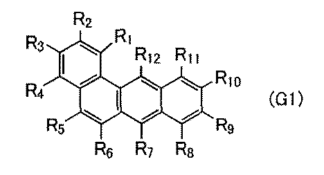


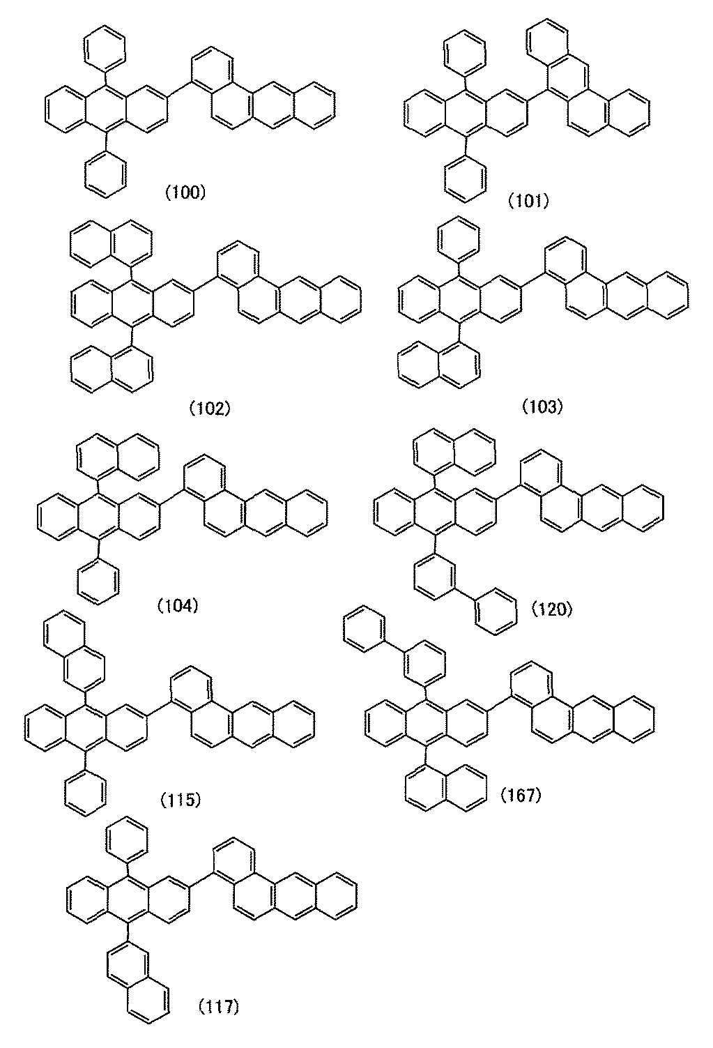
本実施の形態では、本発明の一態様の有機化合物について、以下説明する。


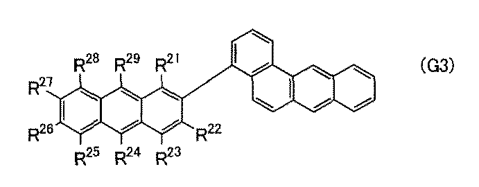
一般式(G1)乃至(G3)及び(g1)において、R1乃至R12及びR21乃至R29は、例えば、水素、炭素数1乃至6のアルキル基、置換もしくは無置換の炭素数3乃至6のシクロアルキル基、または置換もしくは無置換の環を構成する炭素数が6乃至13のアリール基を表す。該アルキル基としては例えば、メチル基、エチル基、プロピル基、イソプロピル基、ブチル基、イソブチル基、tert−ブチル基、n−ヘキシル基などを挙げることができ、該シクロアルキル基としては例えば、シクロプロピル基、シクロブチル基、シクロペンチル基、シクロヘキシル基などを挙げることができ、該アリール基としては、フェニル基、ナフチル基、フルオレニル基、などを具体例として挙げることができる。より具体的には例えば、下記構造式(R−1)乃至(R−22)で表される基が挙げられる。なお、R1乃至R29で表される基はこれらに限定されない。

一般式(G1)乃至(G3)として表される化合物の具体的な構造としては、下記構造式(100)乃至(170)で表される有機化合物等を挙げることができる。なお、一般式(G1)乃至(G3)として表される有機化合物は、下記例示に限られない。
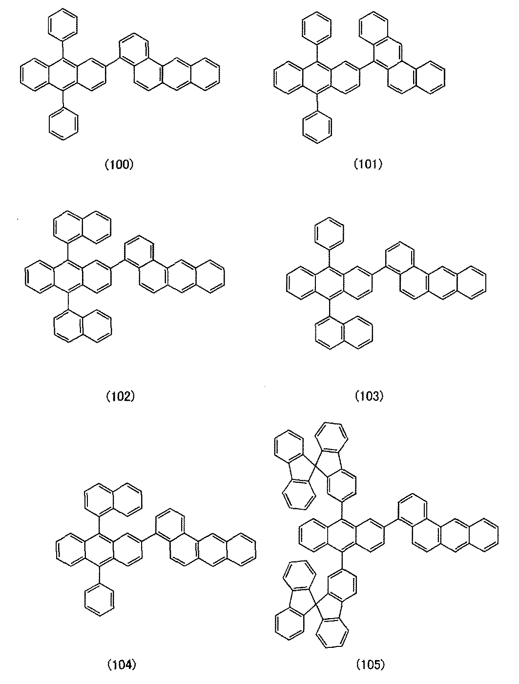


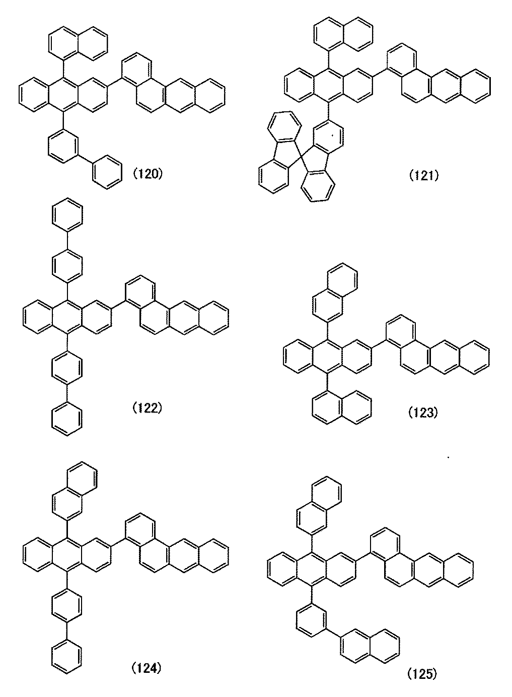
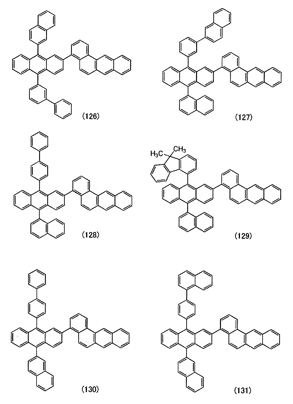
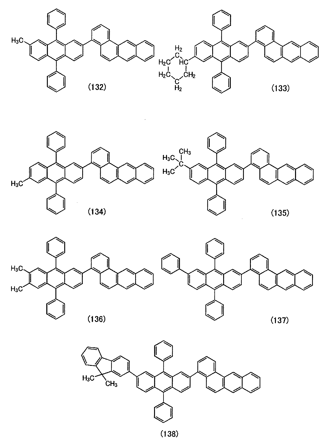
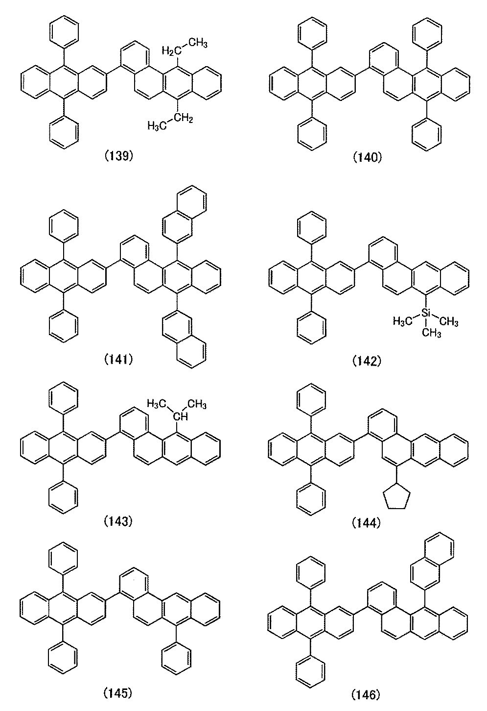

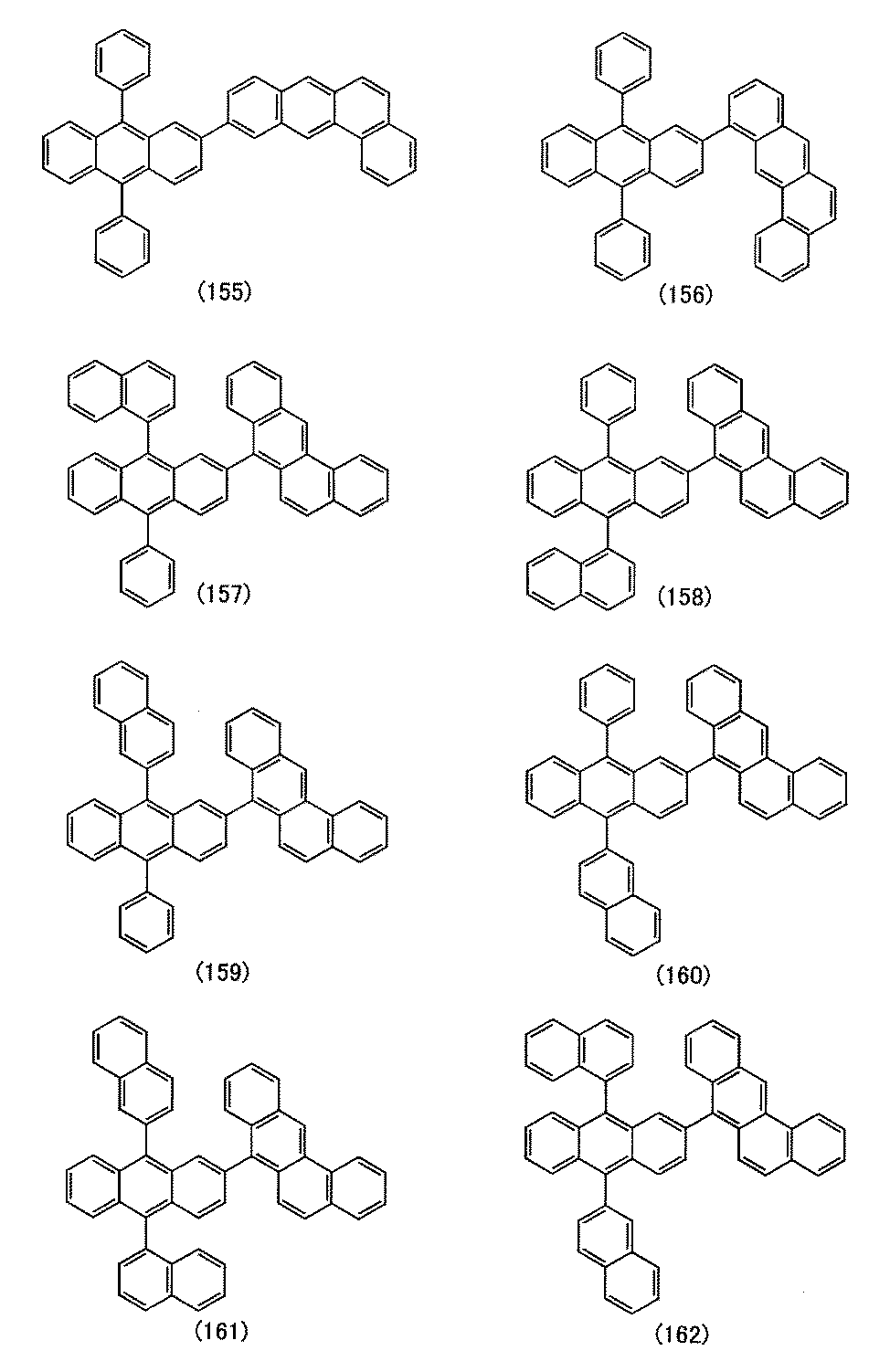

本実施の形態では、本発明の一態様の有機化合物の合成法の一例について、一般式(G1)で表される有機化合物を例に説明する。


本実施の形態では、本発明の一態様である有機化合物を有する発光素子の構成例を、図1を用いて以下に説明する。
次に、上記青色蛍光素子の構成例について図1(A)、図1(B)、図1(C)を用いて説明する。
・Host(141):ホスト材料141
・Guest(142):ゲスト材料142(蛍光材料)
・SFH:ホスト材料141のS1準位
・TFH:ホスト材料141のT1準位
・SFG:ゲスト材料142(蛍光材料)のS1準位
・TFG:ゲスト材料142(蛍光材料)のT1準位
・Energy:エネルギー
・Emission:発光
・quench:消光
ホスト材料141としてベンゾ[a]アントラセン骨格を有する材料を用い、ゲスト材料142が有する発光団にベンゾフラン骨格が含まれる材料を用いると好ましい。該構成の発光素子とすることで、発光効率及び信頼性が良好な発光素子を得ることができる。ベンゾ[a]アントラセン骨格を有する材料としては、一般式(G1)乃至(G3)で表される有機化合物を好適に用いることができる。


次に図1に示す発光素子と異なる発光素子の一例を図2を用いて説明する。図2(A)に示す発光素子152は、少なくとも発光層140に本発明の一態様である有機化合物を用いた素子である。図2(B)は正孔注入層111、正孔輸送層112及び発光層140における材料の構成例を示しており、図2(C)は正孔注入層111、正孔輸送層112及び発光層140における各材料のエネルギー準位の相関を表す模式図である。
・HIM(131):正孔注入層材料131
・HTM(132):第1の正孔輸送材料132
・HTM(133):第2の正孔輸送材料133
・HTM(134):第3の正孔輸送材料134
・Host(141):ホスト材料141
・ゲスト材料142
次に、本発明の一態様に係わる発光素子の構成要素の詳細について、以下説明を行う。
発光層140中では、ホスト材料141が少なくともゲスト材料142より重量比で多く存在し、ゲスト材料142(蛍光材料)は、ホスト材料141中に分散される。なお、発光層140において、ホスト材料141は、一種の化合物から構成されていても良く、複数の化合物から構成されていても良い。
正孔注入層111は、一対の電極の一方(電極101または電極102)からのホール注入障壁を低減することでホール注入を促進する機能を有し、例えば遷移金属酸化物、フタロシアニン誘導体、あるいは芳香族アミンなどによって形成される。遷移金属酸化物としては、モリブデン酸化物やバナジウム酸化物、ルテニウム酸化物、タングステン酸化物、マンガン酸化物などが挙げられる。フタロシアニン誘導体としては、フタロシアニンや金属フタロシアニンなどが挙げられる。芳香族アミンとしてはベンジジン誘導体やフェニレンジアミン誘導体などが挙げられる。ポリチオフェンやポリアニリンなどの高分子化合物を用いることもでき、例えば自己ドープされたポリチオフェンであるポリ(エチレンジオキシチオフェン)/ポリ(スチレンスルホン酸)などがその代表例である。
正孔輸送層112は正孔輸送材料を含む層であり、正孔注入層111の材料として例示した正孔輸送材料を使用することができる。正孔輸送層112は正孔注入層111に注入された正孔を発光層140へ輸送する機能を有するため、正孔注入層111のHOMO準位と同じ、あるいは近いHOMO準位を有することが好ましい。なお、正孔輸送層112が複数の層からなる場合、図2(C)に示すようにHOMO準位が階段状になるように正孔輸送層112に用いる材料が選択されると好ましい。
電子輸送層118は、電子注入層119を経て一対の電極の他方(電極101または電極102)から注入された電子を発光層140へ輸送する機能を有する。電子輸送性材料としては、正孔よりも電子の輸送性の高い材料を用いることができ、1×10⁻⁶cm2/Vs以上の電子移動度を有する材料であることが好ましい。本発明の一態様の有機化合物も好適に用いることができる。電子を受け取りやすい化合物(電子輸送性を有する材料)としては、含窒素複素芳香族化合物のようなπ電子不足型複素芳香族や金属錯体などを用いることができる。具体的には、キノリン配位子、ベンゾキノリン配位子、オキサゾール配位子、あるいはチアゾール配位子を有する金属錯体、オキサジアゾール誘導体、トリアゾール誘導体、ベンゾイミダゾール誘導体、キノキサリン誘導体、ジベンゾキノキサリン誘導体、フェナントロリン誘導体、ピリジン誘導体、ビピリジン誘導体、ピリミジン誘導体、トリアジン誘導体などが挙げられる。なお、正孔よりも電子の輸送性の高い物質であれば、上記以外の物質を電子輸送層として用いても構わない。また、電子輸送層118は、単層のものだけでなく、上記物質からなる層が二層以上積層したものとしてもよい。
電子注入層119は電極102からの電子注入障壁を低減することで電子注入を促進する機能を有し、例えば第1族金属、第2族金属、あるいはこれらの酸化物、ハロゲン化物、炭酸塩などを用いることができる。また、先に示す電子輸送性材料と、これに対して電子供与性を示す材料の複合材料を用いることもできる。電子供与性を示す材料としては、第1族金属、第2族金属、あるいはこれらの酸化物などを挙げることができる。具体的には、フッ化リチウム、フッ化ナトリウム、フッ化セシウム、フッ化カルシウム、リチウム酸化物等のようなアルカリ金属、アルカリ土類金属、またはそれらの化合物を用いることができる。また、フッ化エルビウムのような希土類金属化合物を用いることができる。また、電子注入層119にエレクトライドを用いてもよい。該エレクトライドとしては、例えば、カルシウムとアルミニウムの混合酸化物に電子を高濃度添加した物質等が挙げられる。また、電子注入層119に、電子輸送層118で用いることが出来る物質を用いても良い。
量子ドットは、数nmから数十nmサイズの半導体ナノ結晶であり、1×10³個から1×10⁶個程度の原子から構成されている。量子ドットはサイズに依存してエネルギーシフトするため、同じ物質から構成される量子ドットであっても、サイズによって発光波長が異なる。そのため、用いる量子ドットのサイズを変更することによって、容易に発光波長を変更することができる。
電極101及び電極102は、発光素子の陽極または陰極としての機能を有する。電極101及び電極102は、金属、合金、導電性化合物、及びこれらの混合物や積層体などを用いて形成することができる。
また、本発明の一態様に係る発光素子は、ガラス、プラスチックなどからなる基板上に作製すればよい。基板上に作製する順番としては、電極101側から順に積層しても、電極102側から順に積層しても良い。
本実施の形態においては、実施の形態3に示す発光素子の構成と異なる構成の発光素子について、図3を用いて、以下説明を行う。なお、図3において、図1(A)に示す符号と同様の機能を有する箇所には、同様のハッチパターンとし、符号を省略する場合がある。また、同様の機能を有する箇所には、同様の符号を付し、その詳細な説明は省略する場合がある。
図3は、発光素子250の断面模式図である。
本実施の形態では実施の形態3及び実施の形態4で説明した発光素子を用いた発光装置について、図4(A)及び図4(B)を用いて説明する。
図5には表示装置の一例として、白色発光を呈する発光素子を形成し、着色層(カラーフィルタ)を形成した発光装置の例を示す。
トップエミッション型の発光装置の断面図を図6に示す。この場合、基板1001は光を通さない基板を用いることができる。TFTと発光素子の陽極とを接続する接続電極を作製するまでは、ボトムエミッション型の発光装置と同様に形成する。その後、第3の層間絶縁膜1037を電極1022を覆って形成する。この絶縁膜は平坦化の役割を担っていても良い。第3の層間絶縁膜1037は第2の層間絶縁膜1021と同様の材料の他、他の様々な材料を用いて形成することができる。
本実施の形態では、本発明の一態様の電子機器について説明する。
本実施の形態では、本発明の一態様の発光素子を様々な照明装置に適用する一例について、図11及び図12を用いて説明する。本発明の一態様である発光素子を用いることで、発光効率が良好な、信頼性の高い照明装置を作製できる。
100mL3口フラスコに2−ヨード−9,10−ジフェニルアントラセン1.1g(2.4mmol)、4−ベンゾ[a]アントラセンボロン酸0.80g(2.9mmol)、トリス(2−メチルフェニル)ホスフィン0.17g(0.55mmol)、炭酸カリウム0.71g(5.1mmol)を加え、フラスコ内を窒素置換した。この混合物にトルエン24mL、エタノール3mL、水3mLを加え、減圧下で攪拌する事で脱気した。この混合物に、酢酸パラジウム(II)37mg(0.17mmol)を加え、窒素気流下、80℃で11時間撹拌した。撹拌後、室温まで冷却し、混合物に水を加えて、水層をトルエンで抽出した。得られた有機層を、飽和食塩水で洗浄後、有機層を硫酸マグネシウムで乾燥した。この混合物を濾過し、濾液を濃縮して固体を得た。得られた固体のトルエン溶液をセライト(和光純薬工業株式会社、カタログ番号:537−02305)、フロリジール(和光純薬工業株式会社、カタログ番号:066−05265)、酸化アルミニウムを通して吸引濾過し、濾液を濃縮して固体を得た。得られた固体を、シリカゲルカラムクロマトグラフィー(トルエン:ヘキサン=1:6)で精製し、さらに高速液体クロマトグラフィー(展開溶媒:クロロホルム)で精製した。得られた固体をメタノールで洗浄したところ、目的物の淡黄色粉末を収量1.0g、収率74%で得た。本合成スキームを下記(A−1)に示す。
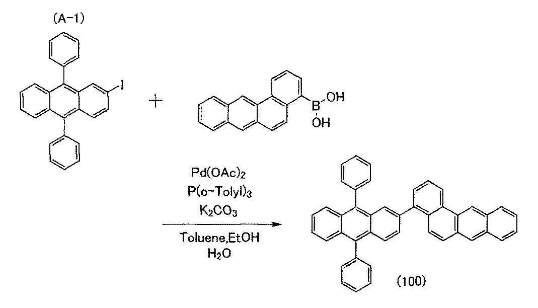
2aBAPAのトルエン溶液の吸収スペクトルと発光スペクトルを図14に示す。また、薄膜の吸収スペクトルと発光スペクトルを図15に示す。固体薄膜は石英基板上に真空蒸着法にて作成した。トルエン溶液の吸収スペクトルの測定には、紫外可視分光光度計((株)日本分光製 V550型)を用いた。トルエンのみを石英セルに入れて測定したトルエンの吸収スペクトルを、2aBAPAのトルエン溶液の吸収スペクトルから差し引くことで、図14に示す2aBAPA溶液の吸収スペクトルを得た。また、薄膜の吸収スペクトルの測定には、分光光度計((株)日立ハイテクノロジーズ製分光光度計U4100)を用いた。また、発光スペクトルの測定には、蛍光光度計((株)浜松ホトニクス製 FS920)を用いた。
200mL3口フラスコに2−ヨード−9,10−ジフェニルアントラセン2.3g(5.0mmol)、ベンゾ[a]アントラセン−7−ボロン酸1.4g(5.0mmol)、トリ(オルト−トリル)ホスフィン0.15g(0.50mmol)、炭酸カリウム1.4g(10mmol)を加え、フラスコ内を窒素置換した。この混合物にトルエン20mL、エタノール5.0mL、水5.0mLを加え、減圧下で攪拌する事で脱気した。この混合物に、酢酸パラジウム(II)56mg(0.25mmol)を加え、窒素気流下、80℃で8時間攪拌した。撹拌後、この混合物の水層をトルエンで抽出し、抽出溶液と有機層を合わせて飽和食塩水で洗浄し、硫酸マグネシウムを加えて乾燥した。この混合物を自然濾過して得たろ液を濃縮して得た油状物をシリカゲルカラムクロマトグラフィー(ヘキサン:トルエン=4:1)で精製し、続いてトルエンで再結晶したところ、目的物の黄色固体を収量2.3g、収率83%で得た。本合成スキームを下記式(A−2)に示す。
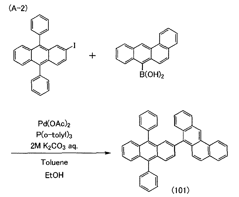
次に、2aBAPA−02のトルエン溶液の吸収スペクトルおよび発光スペクトルを測定した結果を図17に示す。また、薄膜の吸収スペクトルおよび発光スペクトルを図18に示す。測定は実施例1と同様に行った。
200mL3口フラスコに2−ブロモ−9,10−ジ(1−ナフチル)アントラセン1.1g(2.2mmol)、ベンゾ[a]アントラセン−4−ボロン酸0.82g(5.0mmol)、トリ(オルト−トリル)ホスフィン67mg(0.22mmol)、炭酸カリウム0.61g(4.4mmol)を加え、フラスコ内を窒素置換した。この混合物にトルエン9.0mL、エタノール2.0mL、水2.0mLを加え、減圧下で攪拌する事で脱気した。この混合物に、酢酸パラジウム(II)25mg(0.11mmol)を加え、窒素気流下、80℃で4時間攪拌した。撹拌後、この混合物を吸引濾過して得た固体をシリカゲルカラムクロマトグラフィー(ヘキサン:トルエン=4:1)で精製し、続いてトルエンで再結晶したところ、目的物の淡黄色固体を収量1.0g、収率71%で得た。本合成スキームを下記式(A−3)に示す。

次に、2aBAαDNAのトルエン溶液の吸収スペクトルおよび発光スペクトルを測定した結果を図20に示す。また、薄膜の吸収スペクトルおよび発光スペクトルを図21に示す。測定は実施例1と同様に行った。
200mL3口フラスコに2−クロロ−10−(1−ナフチル)−9−フェニルアントラセン2.0g(4.8mmol)、ベンゾ[a]アントラセン−4−ボロン酸1.3g(4.8mmol)、ジ(1−アダマンチル)−n−ブチルホスフィン0.17g(0.48mmol)、リン酸三カリウム3.2g(15mmol)、tert−ブチルアルコール1.1g(15mmol)を加え、フラスコ内を窒素置換した。この混合物にジエチレングリコールジメチルエーテル24mLを加え、減圧下で攪拌する事で脱気した。この混合物に、酢酸パラジウム(II)54mg(0.24mmol)を加え、窒素気流下、140℃で12時間攪拌した。撹拌後、この混合物を吸引濾過して得た固体をトルエンに溶解し、セライト・酸化アルミニウム・フロリジールを通して吸引濾過した。得られたろ液を濃縮して得た固体を、高速液体クロマトグラフィー(HPLC)により精製し、続いてトルエンで再結晶したところ、目的物の淡黄色固体を収量1.2g、収率42%で得た。本合成スキームを下記式(A−4)に示す。
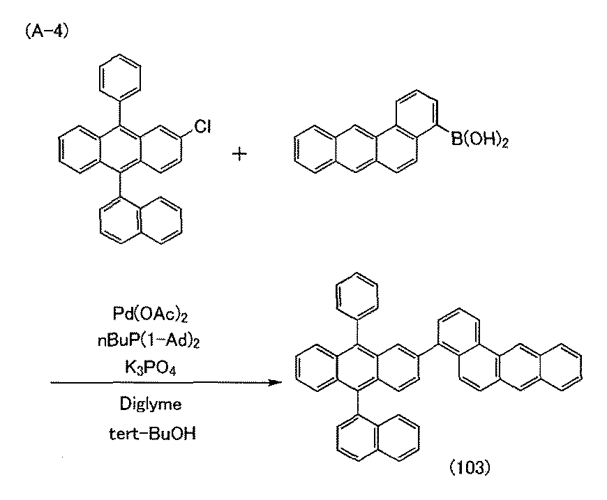
次に、3aBA−αNPhAのトルエン溶液の吸収スペクトルおよび発光スペクトルを測定した結果を図23に示す。また、薄膜の吸収スペクトルおよび発光スペクトルを図24に示す。測定は実施例1と同様に行った。
200mL3口フラスコに2−クロロ−9−(1−ナフチル)−10−フェニルアントラセン3.0g(7.1mmol)、ベンゾ[a]アントラセン−4−ボロン酸2.7g(10mmol)、ジ(1−アダマンチル)−n−ブチルホスフィン0.26g(0.72mmol)、リン酸三カリウム4.5g(21mmol)、tert−ブチルアルコール1.6g(21mmol)を加え、フラスコ内を窒素置換した。この混合物にジエチレングリコールジメチルエーテル36mLを加え、減圧下で攪拌する事で脱気した。この混合物に、酢酸パラジウム(II)80mg(0.36mmol)を加え、窒素気流下、130℃で4時間攪拌した。撹拌後、この混合物を吸引濾過して得た固体をトルエンに溶解し、セライト・酸化アルミニウム・フロリジールを通して吸引濾過した。得られたろ液を濃縮して得た固体を、高速液体クロマトグラフィー(HPLC)により精製し、さらにトルエンで再結晶したところ、目的物の淡黄色固体を収量2.3g、収率52%で得た。本合成スキームを下記式(A−5)に示す。

次に、2aBA−αNPhAのトルエン溶液の吸収スペクトルおよび発光スペクトルを測定した結果を図26に示す。また、薄膜の吸収スペクトルおよび発光スペクトルを図27に示す。測定は実施例1と同様に行った。


ガラス基板上に電極101として、ITSO膜をスパッタリング法にて厚さが70nmになるように形成した。なお、電極101の電極面積は、4mm2(2mm×2mm)とした。次に基板上に発光素子を形成するための前処理として、基板表面を水で洗浄し、200℃で1時間乾燥させた後、UVオゾン処理を370秒行った。その後、1×10⁻⁴Pa程度の真空度に保たれた真空蒸着装置に基板を入れ、170℃で30分間のベークを行った。その後、基板を30分程度放冷した。
発光素子2の作製工程は、先に示した比較発光素子1と発光層140及び電子輸送層118(1)の作製工程のみ異なり、その他の作製工程は比較発光素子1と同様である。発光素子2の素子構造は表2に示す通りであるため、詳細な作製工程に関しては省略する。なお、発光素子2の発光層140及び電子輸送層118(1)は比較発光素子1と同様に真空蒸着法により成膜した。
次に、上記作製した比較発光素子1及び発光素子2の特性を測定した。輝度およびCIE色度の測定には色彩輝度計(トプコン社製、BM−5A)を用い、電界発光スペクトルの測定にはマルチチャンネル分光器(浜松ホトニクス社製、PMA−11)を用いた。

次に、比較発光素子1及び発光素子2の2mAにおける定電流駆動試験を行った。その結果を図32に示す。図32から比較発光素子1及び発光素子2は良好な信頼性を有することが分かった。特に発光素子2はLT90(輝度10%減少時間)が230時間を超えており、特に良好な信頼性を示すことが分かった。また、図32より発光素子2は比較発光素子1よりも良好な信頼性を有することが分かった。よって、アントラセン骨格の2位にベンゾ[a]アントラセン骨格を有する有機化合物を用いた発光素子はアントラセン骨格の2位にフェニル基を有する有機化合物を用いた発光素子よりも良好な信頼性を有することが分かった。
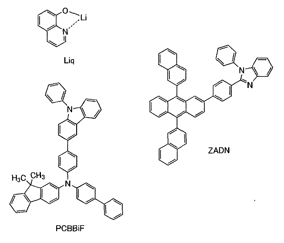
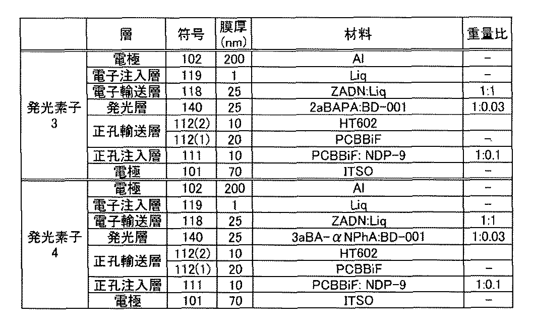
発光素子3の正孔注入層111として、電極101上にPCBBiFと、NDP−9(分析工房株式会社、材料シリアル番号:1S20170124)と、を重量比(PCBBiF:NDP−9)が1:0.1になるように、且つ厚さが10nmになるように共蒸着した。
発光素子4の作製工程は、先に示した発光素子3と発光層140の作製工程のみ異なり、その他の作製工程は発光素子3と同様である。発光素子4の素子構造は表4に示す通りであるため、詳細な作製工程に関しては省略する。なお、発光素子4の発光層140は発光素子4と同様に真空蒸着法により成膜した。
次に、上記作製した発光素子3及び発光素子4の特性を測定した。発光素子の測定条件は先に示す実施例と同様に行った。

次に、発光素子3及び発光素子4の2mAにおける定電流駆動試験を行った。その結果を図37に示す。図37から発光素子3及び発光素子4はLT90が200時間を超えており、良好な信頼性を有することが分かった。また、図37より発光素子4は発光素子3よりも良好な信頼性を有することが分かった。よって、アントラセン骨格の2位にベンゾ[a]アントラセン骨格を有し、さらにアントラセン骨格の9位と10位には異なるアリール基を有する有機化合物を用いた発光素子は、非常に信頼性が良好な発光素子を作製できることが分かった。
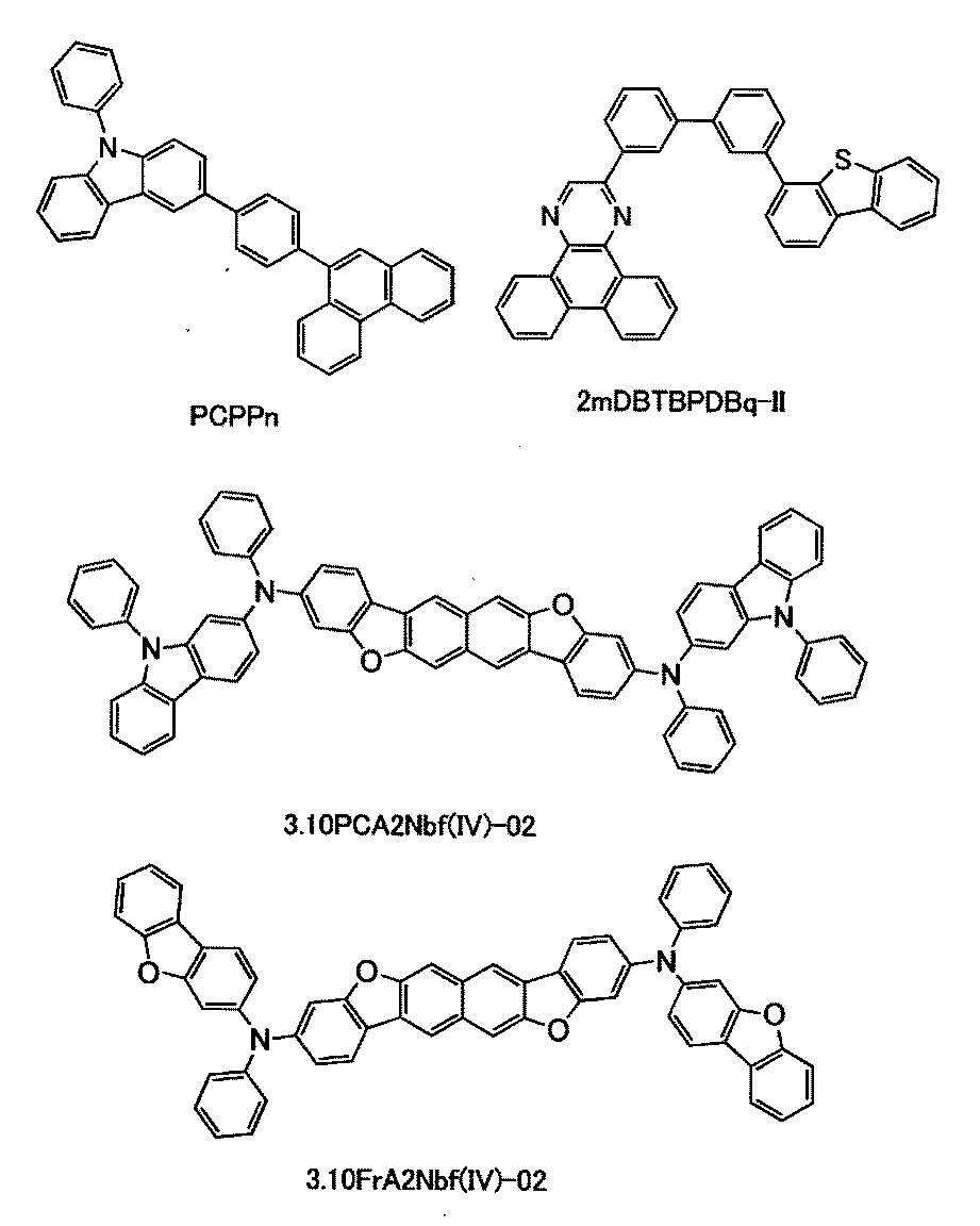

発光素子5の正孔注入層111として、電極101上にPCPPnと、MoO3、を重量比(PCPPn:MoO3)が1:0.5になるように、且つ厚さが10nmになるように共蒸着した。
発光素子6乃至発光素子8の作製工程は、先に示した発光素子5と発光層140の作製工程のみ異なり、その他の作製工程は発光素子5と同様である。発光素子6乃至発光素子8の素子構造は表6に示す通りであるため、詳細な作製工程に関しては省略する。なお、表6中、発光素子6及び発光素子8のゲスト材料としては、3,10−ビス[N−(ジベンゾフラン−3−イル)−N−フェニルアミノ]ナフト[2,3−b;6,7−b’]ビスベンゾフラン(略称:3,10FrA2Nbf(IV)−02)を用いた。また、発光素子6乃至発光素子8の発光層140は発光素子5と同様に真空蒸着法により成膜した。
次に、上記作製した発光素子5乃至発光素子8の特性を測定した。発光素子の測定条件は先に示す実施例と同様に行った。

次に、発光素子5乃至発光素子8の2mAにおける定電流駆動試験を行った。その結果を図42に示す。図42から発光素子5乃至発光素子8はそれぞれ良好な信頼性を有することが分かった。また、同一のゲスト材料を有する発光素子である、発光素子5及び発光素子7、発光素子6及び発光素子8をそれぞれ比較すると、発光素子7及び発光素子8の方が信頼性が良好である。この結果から実施例8と同様に、アントラセン骨格の2位にベンゾ[a]アントラセン骨格を有し、さらにアントラセン骨格の9位と10位には異なるアリール基を有する有機化合物を用いた発光素子は、非常に信頼性が良好な発光素子を作製できることが分かった。
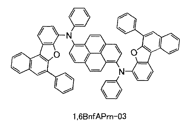

発光素子9及び発光素子10の作製工程は、先に示した発光素子5と発光層140の作製工程のみ異なり、その他の作製工程は発光素子5と同様である。発光素子9及び発光素子10は表8に示す通りであるため、詳細な作製工程に関しては省略する。なお、表8中、発光素子9のゲスト材料としては、N,N’−(ピレン−1,6−ジイル)ビス[(6,N−ジフェニルベンゾ[b]ナフト[1,2−d]フラン)−8−アミン](略称:1,6BnfAPrn−03)を用いた。また、発光素子9及び発光素子10の発光層140は発光素子5と同様に真空蒸着法により成膜した。
次に、上記作製した発光素子9及び発光素子10の特性を測定した。発光素子の測定条件は先に示す実施例と同様に行った。
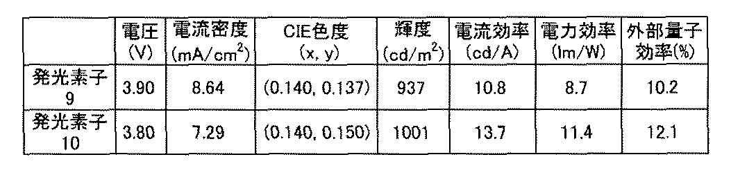
次に、発光素子9及び発光素子10の2mAにおける定電流駆動試験を行った。その結果を図47に示す。図47から発光素子9及び発光素子10は良好な信頼性を有することが分かった。また、図47より発光素子10は発光素子9よりも良好な信頼性を有することが分かった。よって、ベンゾ[a]アントラセン骨格を有するホスト材料に用いた場合、発光団にベンゾフラン骨格を有するゲスト材料を用いた発光素子は、発光団にピレン骨格を用いた発光素子よりも、良好な信頼性を有することが分かった。
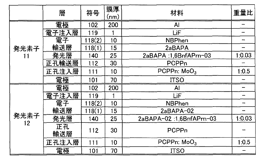
発光素子11の正孔注入層111として、電極101上にPCPPnと、MoO3、を重量比(PCPPn:MoO3)が1:0.5になるように、且つ厚さが10nmになるように共蒸着した。
発光素子12の作製工程は、先に示した発光素子11と発光層140及び電子輸送層118(1)の作製工程のみ異なり、その他の作製工程は発光素子11と同様である。発光素子12の素子構造は表10に示す通りであるため、詳細な作製工程に関しては省略する。また、発光素子11の発光層140及び電子輸送層118(1)は発光素子11と同様に真空蒸着法により成膜した。
次に、上記作製した発光素子11と発光素子12の特性を測定した。発光素子の測定条件は先に示す実施例と同様に行った。

次に、発光素子11と発光素子12の2mAにおける定電流駆動試験を行った。その結果を図52に示す。図52から発光素子11と発光素子12は良好な信頼性を有することが分かった。また、図52より発光素子11は発光素子12よりも良好な信頼性を有することが分かった。よって、ベンゾ[a]アントラセン骨格の4位でアントラセン骨格に結合している有機化合物の方が、ベンゾ[a]アントラセン骨格の7位でアントラセン骨格に結合している有機化合物よりも信頼性が良好な発光素子を作製できることが分かった。

発光素子13の正孔注入層111として、電極101上にPCPPnと、MoO3、を重量比(PCPPn:MoO3)が1:0.5になるように、且つ厚さが10nmになるように共蒸着した。
次に、上記作製した発光素子13の特性を測定した。発光素子の測定条件は先に示す実施例と同様に行った。

次に、発光素子13におけるTTAの効果を調査するため、過渡電界発光測定により蛍光寿命の算出を行った。
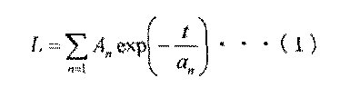
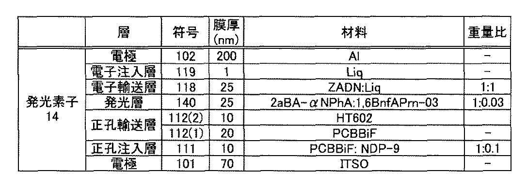
発光素子14の正孔注入層111として、電極101上にPCBBiFと、NDP−9と、を重量比(PCBBiF:NDP−9)が1:0.1になるように、且つ厚さが10nmになるように共蒸着した。
次に、上記作製した発光素子14の特性を測定した。発光素子の測定条件は先に示す実施例と同様に行った。

次に、発光素子14の2mAにおける定電流駆動試験を行った。その結果を図62に示す。図62より発光素子14はLT90が300時間以上である、非常に良好な信頼性を有することが分かった。
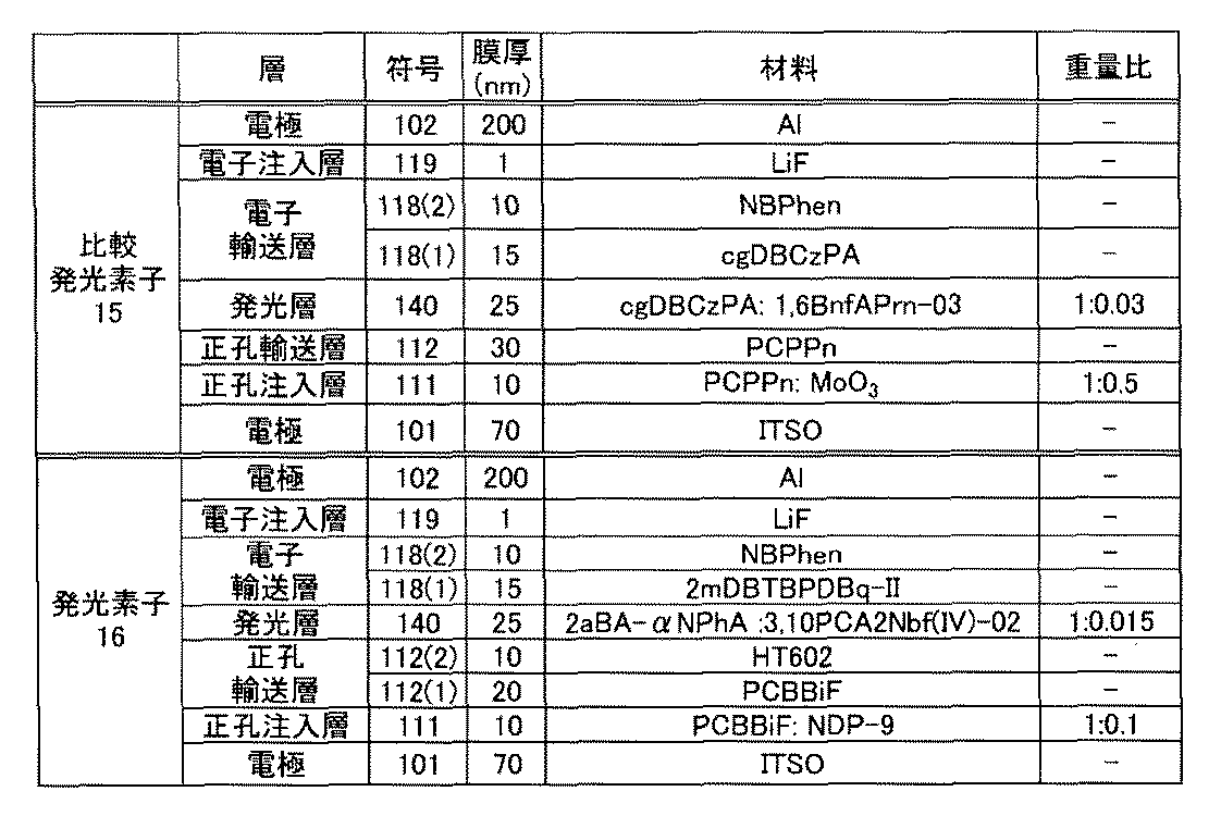
比較発光素子15の正孔注入層111として、電極101上にPCPPnと、MoO3、を重量比(PCPPn:MoO3)が1:0.5になるように、且つ厚さが10nmになるように共蒸着した。
発光素子16の正孔注入層111として、電極101上にPCBBiFと、NDP−9と、を重量比(PCBBiF:NDP−9)が1:0.1になるように、且つ厚さが10nmになるように共蒸着した。
次に、上記作製した比較発光素子15及び発光素子16の特性を測定した。発光素子の測定条件は先に示す実施例と同様に行った。
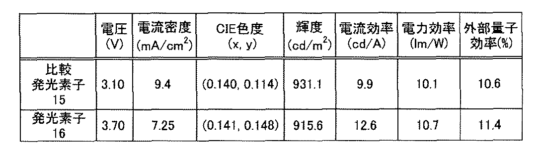
次に、比較発光素子15及び発光素子16の2mAにおける定電流駆動試験を行った。その結果を図67(A)及び(B)に示す。図67(A)は横軸をリニアスケールで表しており、図67(B)は横軸を対数スケールで表している。図67(A)及び(B)より比較発光素子15及び発光素子16は共にLT90が100時間以上である、良好な信頼性を有することが分かった。特に発光素子16はLT90を見積もると400時間を超えており、非常に良好な信頼性を有することが分かった。また、発光素子16は比較発光素子15よりも4倍以上長寿命な素子であることが分かった。
50mL3口フラスコに2−クロロ−9−(1−ナフチル)−10−(3−ビフェニリル)アントラセン1.3g(2.6mmol)、ベンゾ[a]アントラセン−4−ボロン酸0.81g(3.0mmol)、ジ(1−アダマンチル)−n−ブチルホスフィン93mg(0.26mmol)、リン酸三カリウム1.7g(7.8mmol)、tert−ブチルアルコール0.58g(7.8mmol)を加え、フラスコ内を窒素置換した。この混合物にジエチレングリコールジメチルエーテル13mLを加え、減圧下で攪拌する事で脱気した。この混合物に、酢酸パラジウム(II)29mg(0.13mmol)を加え、窒素気流下、120℃で20時間攪拌した。
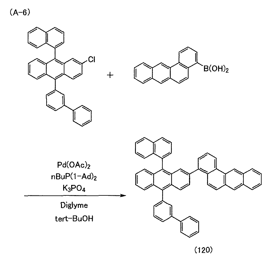
次に、2aBA−αNmBPhAのトルエン溶液の吸収スペクトルおよび発光スペクトルを測定した結果を図69に示す。また、薄膜の吸収スペクトルおよび発光スペクトルを図70に示す。測定は実施例1と同様に行った。
50mL3口フラスコに2−クロロ−9−(2−ナフチル)−10−フェニルアントラセン1.1g(2.7mmol)、ベンゾ[a]アントラセン−4−ボロン酸0.74g(2.7mmol)、ジ(1−アダマンチル)−n−ブチルホスフィン30mg(0.14mmol)、リン酸三カリウム1.7g(8.1mmol)、tert−ブチルアルコール0.60g(8.1mmol)を加え、フラスコ内を窒素置換した。この混合物にジエチレングリコールジメチルエーテル13mLを加え、減圧下で攪拌する事で脱気した。この混合物に、酢酸パラジウム(II)30mg(0.14mmol)を加え、窒素気流下、80℃で8時間攪拌した。

次に、2aBA−βNPhAのトルエン溶液の吸収スペクトルおよび発光スペクトルを測定した結果を図72に示す。また、薄膜の吸収スペクトルおよび発光スペクトルを図73に示す。測定は実施例1と同様に行った。
200mL3口フラスコに2−クロロ−10−(1−ナフチル)−9−(3−ビフェニリル)アントラセン2.3g(4.7mmol)、ベンゾ[a]アントラセン−4−ボロン酸1.4g(5.2mmol)、ジ(1−アダマンチル)−n−ブチルホスフィン0.17g(0.48mmol)、リン酸三カリウム3.0g(14mmol)、tert−ブチルアルコール1.0g(14mmol)を加え、フラスコ内を窒素置換した。この混合物にジエチレングリコールジメチルエーテル24mLを加え、減圧下で攪拌する事で脱気した。この混合物に、酢酸パラジウム(II)54mg(0.24mmol)を加え、窒素気流下、130℃で18時間攪拌した。
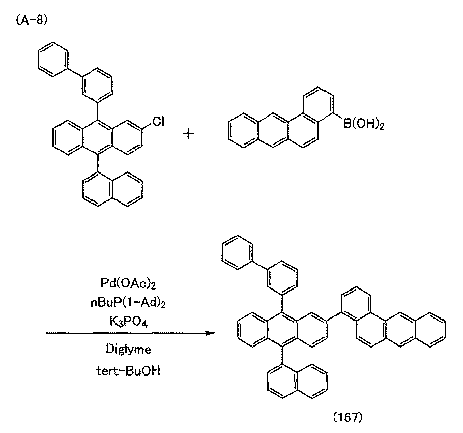
次に、3aBA−αNmBPhAのトルエン溶液の吸収スペクトルおよび発光スペクトルを測定した結果を図75に示す。また、薄膜の吸収スペクトルおよび発光スペクトルを図76に示す。測定は実施例1と同様に行った。
50mL3口フラスコに2−クロロ−10−(2−ナフチル)−9−フェニルアントラセン1.6g(3.9mmol)、ベンゾ[a]アントラセン−4−ボロン酸1.1g(3.9mmol)、ジ(1−アダマンチル)−n−ブチルホスフィン0.14g(0.40mmol)、リン酸三カリウム2.5g(12mmol)、tert−ブチルアルコール0.89g(12mmol)を加え、フラスコ内を窒素置換した。この混合物にジエチレングリコールジメチルエーテル20mLを加え、減圧下で攪拌する事で脱気した。この混合物に、酢酸パラジウム(II)45mg(0.20mmol)を加え、窒素気流下、90℃で14時間攪拌した。
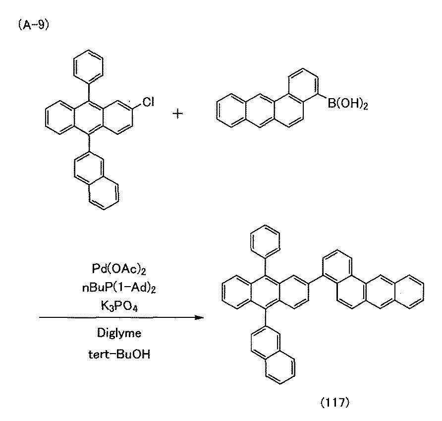
次に、3aBA−βNPhAのトルエン溶液の吸収スペクトルおよび発光スペクトルを測定した結果を図78に示す。また、薄膜の吸収スペクトルおよび発光スペクトルを図79に示す。測定は実施例1と同様に行った。

発光素子17乃至発光素子20は、先に示す発光素子16と、発光層130の構成(発光素子17は電子輸送層118の構成も)のみ異なり、それ以外の工程は、発光素子16と同様の作製方法とした。素子構造の詳細は表18に示す通りであるため、作製方法の詳細は省略する。
次に、上記作製した発光素子17乃至発光素子20の特性を測定した。測定は実施例7と同様に行った。

次に、発光素子17乃至発光素子20の2mAにおける定電流駆動試験を行った。その結果を図84に示す。図84より発光素子17乃至発光素子20はLT90が180時間以上である、良好な信頼性を有することが分かった。特に、発光素子18及び発光素子20はLT90が250時間以上である、とても良好な信頼性を有することが分かった。

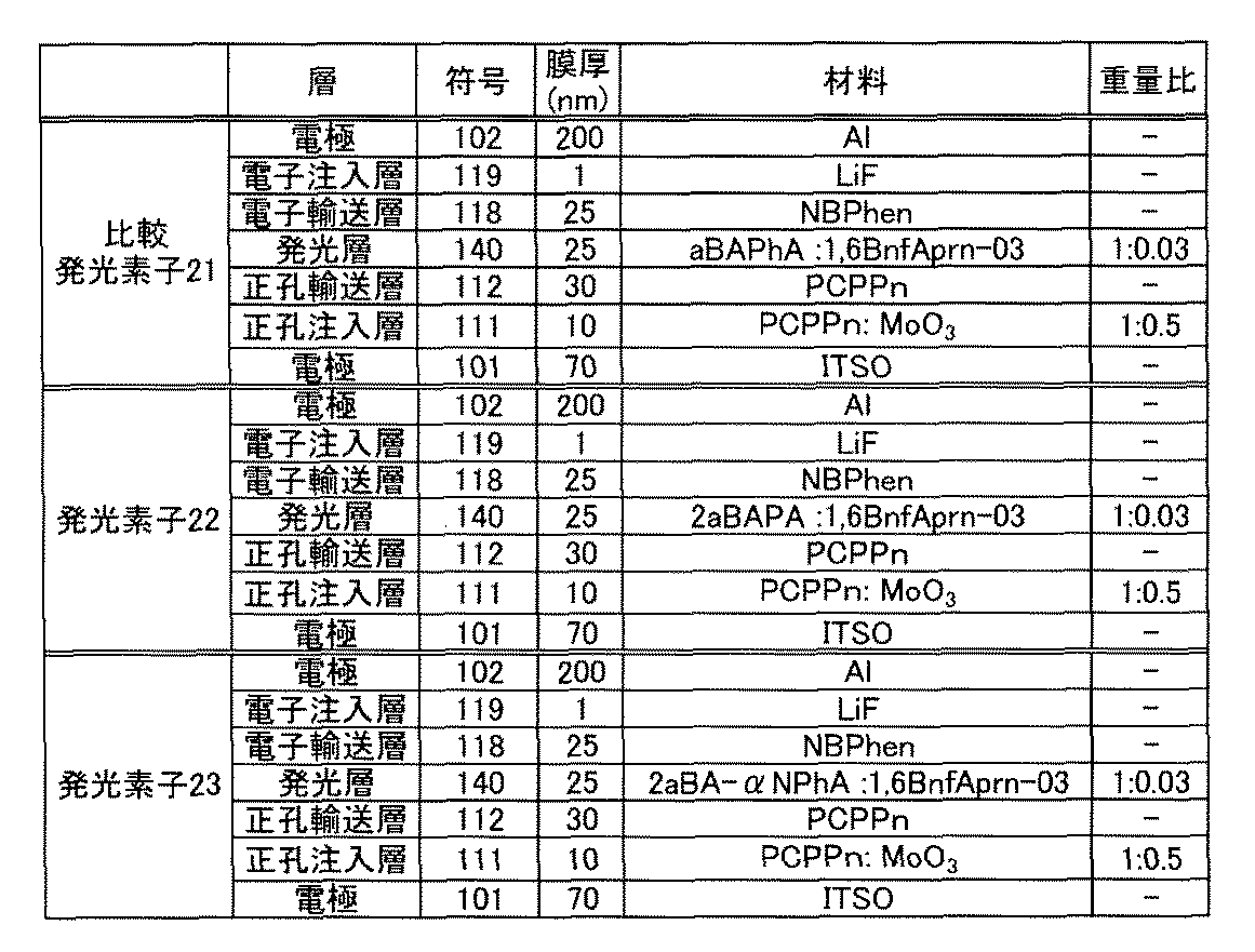
ガラス基板上に電極101として、ITSO膜をスパッタリング法にて厚さが70nmになるように形成した。なお、電極101の電極面積は、4mm2(2mm×2mm)とした。次に基板上に発光素子を形成するための前処理として、基板表面を水で洗浄し、200℃で1時間乾燥させた後、UVオゾン処理を370秒行った。その後、1×10⁻⁴Pa程度の真空度に保たれた真空蒸着装置に基板を入れ、170℃で30分間のベークを行った。その後、基板を30分程度放冷した。
発光素子22及び発光素子23の作製工程は、先に示した比較発光素子21と発光層140の作製工程のみ異なり、その他の作製工程は比較発光素子20と同様である。発光素子22及び発光素子23の素子構造は表20に示す通りであるため、詳細な作製工程に関しては省略する。
比較発光素子21、発光素子22及び発光素子23の2mAにおける定電流駆動試験を行った。その結果を図85に示す。図85より発光素子22及び発光素子23は比較発光素子21よりも良好な信頼性を有していることが分かった。よって、青色蛍光素子に用いるホスト材料としては、ベンゾアントラセン骨格がアントラセン骨格の9位において結合している化合物よりも、ベンゾアントラセン骨格がアントラセン骨格の2位において結合している化合物の方が良好な信頼性を示すことが分かった。
Claims (14)
- 置換または無置換のベンゾ[a]アントラセン骨格と置換または無置換のアントラセン骨格を有し、前記ベンゾ[a]アントラセン骨格は前記アントラセン骨格の2位で結合する、有機化合物。
- 下記一般式(G1)で表される有機化合物。


- 下記一般式(G2)で表される有機化合物。
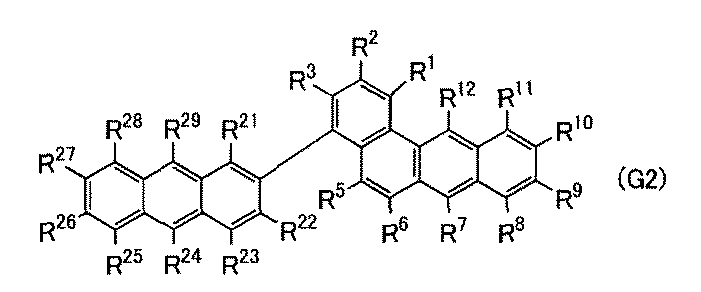
- 下記一般式(G3)で表される有機化合物。
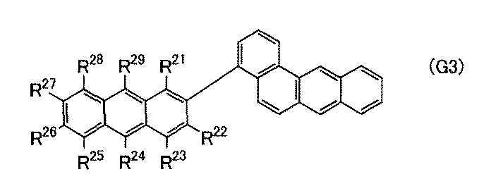
- 請求項2乃至請求項4のいずれか一項において、
前記一般式(G1)乃至前記一般式(G3)中、R24及びR29は、それぞれ独立に炭素数6乃至13の置換もしくは無置換のアリール基である、有機化合物。 - 請求項2乃至請求項4のいずれか一項において、
前記一般式(G1)乃至前記一般式(G3)中、R24及びR29は、それぞれ独立に置換若しくは無置換のフェニル基または、置換若しくは無置換のナフチル基である、有機化合物。 - 請求項2乃至請求項4のいずれか一項において、
前記一般式(G1)乃至前記一般式(G3)中、R24は置換若しくは無置換のフェニル基であり、R29は置換若しくは無置換のナフチル基である、有機化合物。 - 下記構造式(100)乃至(104)、(115)、(117)、(120)及び(167)のいずれか一で表される有機化合物。

- 一対の電極間にEL層を有し、
前記EL層は請求項1乃至請求項8のいずれか一に記載の有機化合物を含む、発光素子。 - 一対の電極間に発光層を有し、
前記発光層は請求項1乃至請求項8のいずれか一に記載の有機化合物を含む、発光素子。 - 一対の電極間に発光層を有し、
前記発光層はホスト材料とゲスト材料を有し、
前記ホスト材料はベンゾ[a]アントラセン骨格を有し、
前記ゲスト材料は発光団を有し、
前記発光団はベンゾフラン骨格を有する、発光素子。 - 請求項9乃至請求項11のいずれか一項に記載の発光素子と、
カラーフィルタおよびトランジスタの少なくとも一と、
を有する発光装置。 - 請求項12に記載の発光装置と、
筐体およびタッチセンサの少なくとも一と、
を有する電子機器。 - 請求項9乃至請求項11のいずれか一項に記載の発光素子と、
筐体およびタッチセンサの少なくとも一と、
を有する照明装置。
Priority Applications (5)
| Application Number | Priority Date | Filing Date | Title |
|---|---|---|---|
| JP2020521635A JP6770664B2 (ja) | 2018-05-31 | 2019-05-22 | 有機化合物、発光素子、発光装置、電子機器、および照明装置 |
| KR1020207037000A KR102802338B1 (ko) | 2018-05-31 | 2019-05-22 | 유기 화합물, 발광 소자, 발광 장치, 전자 기기, 및 조명 장치 |
| CN201980036550.XA CN112204002A (zh) | 2018-05-31 | 2019-05-22 | 有机化合物、发光元件、发光装置、电子设备及照明装置 |
| US17/057,830 US11937498B2 (en) | 2018-05-31 | 2019-05-22 | Organic compound, light-emitting device, light-emitting apparatus, electronic apparatus, and lighting apparatus |
| DE112019002747.6T DE112019002747T5 (de) | 2018-05-31 | 2019-05-22 | Organische Verbindung, Licht emittierendes Element, Licht emittierende Vorrichtung, elektronisches Gerät und Beleuchtungsvorrichtung |
Applications Claiming Priority (4)
| Application Number | Priority Date | Filing Date | Title |
|---|---|---|---|
| JP2018104950 | 2018-05-31 | ||
| JP2018-104950 | 2018-05-31 | ||
| JP2018154845 | 2018-08-21 | ||
| JP2018-154845 | 2018-08-21 |
Publications (1)
| Publication Number | Publication Date |
|---|---|
| WO2019229591A1 true WO2019229591A1 (ja) | 2019-12-05 |
Family
ID=68697883
Family Applications (1)
| Application Number | Title | Priority Date | Filing Date |
|---|---|---|---|
| PCT/IB2019/054218 Ceased WO2019229591A1 (ja) | 2018-05-31 | 2019-05-22 | 有機化合物、発光素子、発光装置、電子機器、および照明装置 |
Country Status (6)
| Country | Link |
|---|---|
| US (1) | US11937498B2 (ja) |
| JP (2) | JP6770664B2 (ja) |
| KR (1) | KR102802338B1 (ja) |
| CN (1) | CN112204002A (ja) |
| DE (1) | DE112019002747T5 (ja) |
| WO (1) | WO2019229591A1 (ja) |
Cited By (1)
| Publication number | Priority date | Publication date | Assignee | Title |
|---|---|---|---|---|
| US20210336149A1 (en) * | 2019-12-25 | 2021-10-28 | Idemitsu Kosan Co.,Ltd. | Organic electroluminescent element and electronic device |
Families Citing this family (3)
| Publication number | Priority date | Publication date | Assignee | Title |
|---|---|---|---|---|
| CN114765201A (zh) * | 2020-12-31 | 2022-07-19 | Tcl科技集团股份有限公司 | 一种显示器件及其像素点亮控制方法 |
| CN117343078A (zh) | 2021-11-25 | 2024-01-05 | 北京夏禾科技有限公司 | 有机电致发光材料和器件 |
| CN115394933A (zh) * | 2022-09-15 | 2022-11-25 | 上海辉纳思光电科技有限公司 | 基于蒽-苯并咪唑为核的光电材料制备的量子点发光器件 |
Citations (5)
| Publication number | Priority date | Publication date | Assignee | Title |
|---|---|---|---|---|
| JP2010528070A (ja) * | 2007-05-29 | 2010-08-19 | メルク パテント ゲーエムベーハー | 有機エレクトロルミネセンス素子のための新規な材料 |
| JP2013521670A (ja) * | 2010-03-09 | 2013-06-10 | メルク パテント ゲーエムベーハー | 電子デバイス用材料 |
| JP2013232521A (ja) * | 2012-04-27 | 2013-11-14 | Udc Ireland Ltd | 有機電界発光素子、有機電界発光素子用材料並びに該有機電界発光素子を用いた発光装置、表示装置及び照明装置 |
| JP2015042636A (ja) * | 2013-07-26 | 2015-03-05 | 株式会社半導体エネルギー研究所 | 有機化合物、発光素子、発光装置、電子機器、および照明装置 |
| JP2017514807A (ja) * | 2014-04-16 | 2017-06-08 | メルク、パテント、ゲゼルシャフト、ミット、ベシュレンクテル、ハフツングMerck Patent GmbH | 電子デバイス用材料 |
Family Cites Families (37)
| Publication number | Priority date | Publication date | Assignee | Title |
|---|---|---|---|---|
| JP2000178548A (ja) | 1998-12-16 | 2000-06-27 | Toppan Printing Co Ltd | 発光材料 |
| JP4404473B2 (ja) | 2000-12-25 | 2010-01-27 | 富士フイルム株式会社 | 新規含窒素へテロ環化合物、発光素子材料およびそれらを使用した発光素子 |
| CN1984889B (zh) | 2004-04-30 | 2011-08-24 | 富士胶片株式会社 | 有机金属络合物、发光性固体、有机el元件及有机el显示器 |
| TWI373506B (en) | 2004-05-21 | 2012-10-01 | Toray Industries | Light-emitting element material and light-emitting material |
| DE102004034140A1 (de) | 2004-07-15 | 2006-02-23 | Covion Organic Semiconductors Gmbh | Verwendung von Polymeren für Up-conversion und Vorrichtungen zur Up-conversion |
| ATE499425T1 (de) | 2004-09-02 | 2011-03-15 | Lg Chemical Ltd | Anthracenderivate und deren verwendung als lichtemittierendes material in organischer lichtemittierender vorrichtung |
| TWI283549B (en) * | 2005-09-30 | 2007-07-01 | Univision Technology Inc | Organic electroluminescent display device with improved color saturation and method of fabricating the same |
| JP4995475B2 (ja) | 2006-04-03 | 2012-08-08 | 出光興産株式会社 | ベンズアントラセン誘導体、及びそれを用いた有機エレクトロルミネッセンス素子 |
| EP1863105B1 (en) | 2006-06-02 | 2020-02-19 | Semiconductor Energy Laboratory Co., Ltd. | Light-emitting element, light-emitting device, and electronic device |
| CN102089282A (zh) | 2008-07-08 | 2011-06-08 | 株式会社半导体能源研究所 | 咔唑衍生物、发光元件用材料、发光元件以及发光装置 |
| CN101445422B (zh) | 2008-12-31 | 2013-06-12 | 清华大学 | 一种有机电致发光材料及其应用 |
| US8476823B2 (en) | 2009-05-22 | 2013-07-02 | Idemitsu Kosan Co., Ltd. | Organic electroluminescent device |
| US20100295444A1 (en) | 2009-05-22 | 2010-11-25 | Idemitsu Kosan Co., Ltd. | Organic electroluminescence device |
| DE102009034625A1 (de) | 2009-07-27 | 2011-02-03 | Merck Patent Gmbh | Neue Materialien für organische Elektrolumineszenzvorrichtungen |
| CN106058048B (zh) * | 2009-09-16 | 2018-11-30 | 默克专利有限公司 | 用于制造电子器件的化合物和电子器件及其制造方法 |
| DE102009053191A1 (de) | 2009-11-06 | 2011-05-12 | Merck Patent Gmbh | Materialien für elektronische Vorrichtungen |
| US8771840B2 (en) | 2009-11-13 | 2014-07-08 | Semiconductor Energy Laboratory Co., Ltd. | Heterocyclic compound, light-emitting element, light-emitting device, electronic device, and lighting device |
| US20110137088A1 (en) | 2009-12-03 | 2011-06-09 | Bp Corporation North America Inc. | Methods and Apparatuses for Producing Renewable Materials From Inhibiting Compounds |
| KR20120100709A (ko) | 2010-01-15 | 2012-09-12 | 이데미쓰 고산 가부시키가이샤 | 유기 전계 발광 소자 |
| ES2654363T3 (es) | 2010-02-22 | 2018-02-13 | University Of Connecticut | Derivados de AMP para tratar enfermedades cardíacas |
| KR20110103819A (ko) | 2010-03-15 | 2011-09-21 | (주)씨에스엘쏠라 | 유기 광소자 및 이를 위한 유기 광합물 |
| JP2011204801A (ja) | 2010-03-24 | 2011-10-13 | Toshiba Mobile Display Co Ltd | 有機エレクトロルミネッセンス装置 |
| CN102859738B (zh) * | 2010-04-12 | 2016-08-03 | 默克专利有限公司 | 具有改进的性能的组合物 |
| KR101778825B1 (ko) * | 2010-05-03 | 2017-09-14 | 메르크 파텐트 게엠베하 | 제형물 및 전자 소자 |
| US9142782B2 (en) | 2010-06-25 | 2015-09-22 | Cambridge Display Technology, Ltd. | Organic light-emitting material, device and method |
| JP5768276B2 (ja) | 2010-09-09 | 2015-08-26 | 公立大学法人大阪府立大学 | ビス(アミノビフェニルエチニル)系化合物、青色蛍光色素および有機el素子 |
| US9324950B2 (en) | 2010-11-22 | 2016-04-26 | Idemitsu Kosan Co., Ltd. | Organic electroluminescence device |
| DE102010054316A1 (de) | 2010-12-13 | 2012-06-14 | Merck Patent Gmbh | Substituierte Tetraarylbenzole |
| JP5780132B2 (ja) * | 2011-05-19 | 2015-09-16 | Jnc株式会社 | ベンゾフルオレン化合物、該化合物を用いた発光層用材料および有機電界発光素子 |
| JP5959970B2 (ja) | 2012-07-20 | 2016-08-02 | 出光興産株式会社 | 有機エレクトロルミネッセンス素子 |
| JP6113993B2 (ja) | 2012-10-03 | 2017-04-12 | 出光興産株式会社 | 有機エレクトロルミネッセンス素子 |
| KR102407604B1 (ko) | 2013-05-16 | 2022-06-13 | 가부시키가이샤 한도오따이 에네루기 켄큐쇼 | 발광 소자, 발광 장치, 전자 기기, 및 조명 장치 |
| EP3117470B1 (de) | 2014-03-13 | 2020-12-23 | Merck Patent GmbH | Organische elektrolumineszenzvorrichtung |
| US10950803B2 (en) | 2014-10-13 | 2021-03-16 | Universal Display Corporation | Compounds and uses in devices |
| US10236448B2 (en) | 2014-10-31 | 2019-03-19 | Semiconductor Energy Laboratory Co., Ltd. | Benzo[a] anthracene compound, light-emitting element, display device, electronic device, and lighting device |
| US10381569B2 (en) * | 2014-11-25 | 2019-08-13 | Universal Display Corporation | Organic electroluminescent materials and devices |
| US10340470B2 (en) * | 2016-02-23 | 2019-07-02 | Semiconductor Energy Laboratory Co., Ltd. | Light-emitting element, display device, electronic device, and lighting apparatus |
-
2019
- 2019-05-22 DE DE112019002747.6T patent/DE112019002747T5/de active Pending
- 2019-05-22 JP JP2020521635A patent/JP6770664B2/ja active Active
- 2019-05-22 KR KR1020207037000A patent/KR102802338B1/ko active Active
- 2019-05-22 WO PCT/IB2019/054218 patent/WO2019229591A1/ja not_active Ceased
- 2019-05-22 CN CN201980036550.XA patent/CN112204002A/zh active Pending
- 2019-05-22 US US17/057,830 patent/US11937498B2/en active Active
-
2020
- 2020-09-25 JP JP2020160960A patent/JP7316986B2/ja active Active
Patent Citations (5)
| Publication number | Priority date | Publication date | Assignee | Title |
|---|---|---|---|---|
| JP2010528070A (ja) * | 2007-05-29 | 2010-08-19 | メルク パテント ゲーエムベーハー | 有機エレクトロルミネセンス素子のための新規な材料 |
| JP2013521670A (ja) * | 2010-03-09 | 2013-06-10 | メルク パテント ゲーエムベーハー | 電子デバイス用材料 |
| JP2013232521A (ja) * | 2012-04-27 | 2013-11-14 | Udc Ireland Ltd | 有機電界発光素子、有機電界発光素子用材料並びに該有機電界発光素子を用いた発光装置、表示装置及び照明装置 |
| JP2015042636A (ja) * | 2013-07-26 | 2015-03-05 | 株式会社半導体エネルギー研究所 | 有機化合物、発光素子、発光装置、電子機器、および照明装置 |
| JP2017514807A (ja) * | 2014-04-16 | 2017-06-08 | メルク、パテント、ゲゼルシャフト、ミット、ベシュレンクテル、ハフツングMerck Patent GmbH | 電子デバイス用材料 |
Cited By (2)
| Publication number | Priority date | Publication date | Assignee | Title |
|---|---|---|---|---|
| US20210336149A1 (en) * | 2019-12-25 | 2021-10-28 | Idemitsu Kosan Co.,Ltd. | Organic electroluminescent element and electronic device |
| US11997920B2 (en) * | 2019-12-25 | 2024-05-28 | Idemitsu Kosan Co., Ltd. | Organic electroluminescent element and electronic device |
Also Published As
| Publication number | Publication date |
|---|---|
| JPWO2019229591A1 (ja) | 2020-12-10 |
| US20210119133A1 (en) | 2021-04-22 |
| KR102802338B1 (ko) | 2025-04-29 |
| JP6770664B2 (ja) | 2020-10-14 |
| JP7316986B2 (ja) | 2023-07-28 |
| US11937498B2 (en) | 2024-03-19 |
| KR20210018315A (ko) | 2021-02-17 |
| DE112019002747T5 (de) | 2021-02-25 |
| JP2021002676A (ja) | 2021-01-07 |
| CN112204002A (zh) | 2021-01-08 |
Similar Documents
| Publication | Publication Date | Title |
|---|---|---|
| JP7106366B2 (ja) | 有機化合物、発光素子、発光装置、電子機器、および照明装置 | |
| JP7257952B2 (ja) | 電子デバイス、表示装置、電子機器、及び照明装置 | |
| JP7140479B2 (ja) | 有機化合物、発光素子、発光装置、電子機器、及び照明装置 | |
| JP7353440B2 (ja) | 化合物 | |
| JP7354387B2 (ja) | 発光素子、表示装置、電子機器及び照明装置 | |
| JP7304818B2 (ja) | 発光素子、発光装置、電子機器、及び照明装置 | |
| JP2018104413A (ja) | 有機化合物、発光素子、発光装置、電子機器、及び照明装置 | |
| JP7316986B2 (ja) | 発光素子、発光装置、電子機器、及び照明装置 | |
| JP7490833B2 (ja) | 有機化合物および発光素子 | |
| WO2020165694A1 (ja) | ホスト材料用アントラセン化合物、発光デバイス、発光装置、電子機器および照明装置 | |
| JP2018104359A (ja) | 有機化合物、発光素子、発光装置、電子機器、および照明装置 |
Legal Events
| Date | Code | Title | Description |
|---|---|---|---|
| 121 | Ep: the epo has been informed by wipo that ep was designated in this application |
Ref document number: 19812238 Country of ref document: EP Kind code of ref document: A1 |
|
| ENP | Entry into the national phase |
Ref document number: 2020521635 Country of ref document: JP Kind code of ref document: A |
|
| ENP | Entry into the national phase |
Ref document number: 20207037000 Country of ref document: KR Kind code of ref document: A |
|
| 122 | Ep: pct application non-entry in european phase |
Ref document number: 19812238 Country of ref document: EP Kind code of ref document: A1 |