WO2019194234A1 - 反射低減装置 - Google Patents
反射低減装置 Download PDFInfo
- Publication number
- WO2019194234A1 WO2019194234A1 PCT/JP2019/014841 JP2019014841W WO2019194234A1 WO 2019194234 A1 WO2019194234 A1 WO 2019194234A1 JP 2019014841 W JP2019014841 W JP 2019014841W WO 2019194234 A1 WO2019194234 A1 WO 2019194234A1
- Authority
- WO
- WIPO (PCT)
- Prior art keywords
- patch
- conductor
- wave
- reflection
- polarization
- Prior art date
- Legal status (The legal status is an assumption and is not a legal conclusion. Google has not performed a legal analysis and makes no representation as to the accuracy of the status listed.)
- Ceased
Links
Images








Classifications
-
- H—ELECTRICITY
- H01—ELECTRIC ELEMENTS
- H01Q—ANTENNAS, i.e. RADIO AERIALS
- H01Q15/00—Devices for reflection, refraction, diffraction or polarisation of waves radiated from an antenna, e.g. quasi-optical devices
- H01Q15/24—Polarising devices; Polarisation filters
-
- H—ELECTRICITY
- H01—ELECTRIC ELEMENTS
- H01Q—ANTENNAS, i.e. RADIO AERIALS
- H01Q1/00—Details of, or arrangements associated with, antennas
- H01Q1/27—Adaptation for use in or on movable bodies
- H01Q1/32—Adaptation for use in or on road or rail vehicles
- H01Q1/3208—Adaptation for use in or on road or rail vehicles characterised by the application wherein the antenna is used
- H01Q1/3233—Adaptation for use in or on road or rail vehicles characterised by the application wherein the antenna is used particular used as part of a sensor or in a security system, e.g. for automotive radar, navigation systems
-
- H—ELECTRICITY
- H01—ELECTRIC ELEMENTS
- H01Q—ANTENNAS, i.e. RADIO AERIALS
- H01Q1/00—Details of, or arrangements associated with, antennas
- H01Q1/36—Structural form of radiating elements, e.g. cone, spiral, umbrella; Particular materials used therewith
- H01Q1/38—Structural form of radiating elements, e.g. cone, spiral, umbrella; Particular materials used therewith formed by a conductive layer on an insulating support
-
- H—ELECTRICITY
- H01—ELECTRIC ELEMENTS
- H01Q—ANTENNAS, i.e. RADIO AERIALS
- H01Q1/00—Details of, or arrangements associated with, antennas
- H01Q1/48—Earthing means; Earth screens; Counterpoises
-
- H—ELECTRICITY
- H01—ELECTRIC ELEMENTS
- H01Q—ANTENNAS, i.e. RADIO AERIALS
- H01Q1/00—Details of, or arrangements associated with, antennas
- H01Q1/52—Means for reducing coupling between antennas; Means for reducing coupling between an antenna and another structure
-
- H—ELECTRICITY
- H01—ELECTRIC ELEMENTS
- H01Q—ANTENNAS, i.e. RADIO AERIALS
- H01Q1/00—Details of, or arrangements associated with, antennas
- H01Q1/52—Means for reducing coupling between antennas; Means for reducing coupling between an antenna and another structure
- H01Q1/528—Means for reducing coupling between antennas; Means for reducing coupling between an antenna and another structure reducing the re-radiation of a support structure
-
- H—ELECTRICITY
- H01—ELECTRIC ELEMENTS
- H01Q—ANTENNAS, i.e. RADIO AERIALS
- H01Q15/00—Devices for reflection, refraction, diffraction or polarisation of waves radiated from an antenna, e.g. quasi-optical devices
- H01Q15/24—Polarising devices; Polarisation filters
- H01Q15/242—Polarisation converters
- H01Q15/246—Polarisation converters rotating the plane of polarisation of a linear polarised wave
-
- H—ELECTRICITY
- H01—ELECTRIC ELEMENTS
- H01Q—ANTENNAS, i.e. RADIO AERIALS
- H01Q21/00—Antenna arrays or systems
- H01Q21/06—Arrays of individually energised antenna units similarly polarised and spaced apart
- H01Q21/061—Two dimensional planar arrays
- H01Q21/065—Patch antenna array
-
- H—ELECTRICITY
- H01—ELECTRIC ELEMENTS
- H01Q—ANTENNAS, i.e. RADIO AERIALS
- H01Q21/00—Antenna arrays or systems
- H01Q21/24—Combinations of antenna units polarised in different directions for transmitting or receiving circularly and elliptically polarised waves or waves linearly polarised in any direction
Definitions
- This disclosure relates to a technique for reducing the influence of reflected waves.
- the reflect array of Patent Document 1 includes a phase difference of reflected waves from elements adjacent in the x-axis direction among a plurality of elements that reflect incident waves, and a level of reflected waves from elements adjacent in the y-axis direction. By controlling the phase difference, an incident wave from the first direction can be reflected in an arbitrary second direction.
- reflected waves may adversely affect the radio wave environment.
- the reflected wave generated by the re-reflection may interfere with the radiated wave, whereby the radiated wave may be attenuated. Therefore, when the reflect array of Patent Document 1 is applied to suppress the influence of the reflected wave, the influence of the reflected wave can be reduced by directing the reflected wave in a direction different from the radiated wave.
- the reflect array of Patent Document 1 only changes the reflection direction from the incident direction, and does not reduce reflected waves that may have an effect. A problem has been found that the effects may not be sufficiently reduced.
- one aspect of the present disclosure can provide a reflection reducing device that effectively reduces the influence of reflected waves.
- a reflection reduction device which includes a dielectric substrate, a first patch group, a second patch group, and a ground plane.
- the dielectric substrate has a first surface and a second surface.
- the first patch group is provided on the first surface and includes a plurality of first conductor patches.
- the second patch group is provided on the first surface and includes a plurality of second conductor patches.
- the ground plane is provided on the second surface and acts as a ground plane.
- Each of the plurality of first conductor patches is insulated, and a current excited by an incoming wave, which is a radio wave coming from the outside, resonates in a direction including at least the first direction and the second direction, and the first direction And the resonance length in the second direction have different patch shapes.
- the plurality of second conductor patches include two or more kinds of conductor patches including at least one first direction patch and at least one second direction patch, and the first conductor patch extends along the outer edge of the first patch group. It is provided at a position separated from the patch group.
- the first direction patch has a shape in which the direction in which the current resonates is limited to the first direction.
- the direction in which the current resonates is limited to the second direction, and the second direction patch has a shape having a resonance length different from that of the first direction patch.
- the first patch group and the second patch group are provided on the first surface of the dielectric substrate.
- the plurality of first conductor patches included in the first patch group have shapes in which the excited current resonates at least in the first direction and the second direction, and the resonance lengths in the two directions are different. Therefore, there is a phase difference between the reflection phase in the first direction and the reflection phase in the second direction of the first conductor patch.
- the polarization direction of the reflected wave generated by reflecting the incoming wave by the plurality of first conductor patches is converted into a direction different from the polarization direction of the incoming wave. Therefore, the first patch group can reduce the influence of the reflected wave.
- the plurality of second conductor patches included in the second patch group converts the polarization direction of the reflected wave into a direction different from the polarization direction of the incoming wave by a combination of the first direction patch and the second direction patch.
- the influence of the reflected wave can be reduced.
- the first direction patch and the second direction patch each have a shape that resonates only in one direction, and is smaller than the first conductor patch that resonates in at least two directions. Therefore, the first direction patch and the second direction patch can be arranged in a narrow space where the first conductor patch cannot be arranged. That is, the first direction patch and the second direction patch can be arranged outside the first patch group having no space for arranging the first conductor patch. Thereby, the influence of a reflected wave can be reduced effectively.
- FIG. 2 is a vertical sectional view showing a section taken along line II-II in FIG. 1. It is a figure explaining the rotation action of the polarization by a conductor patch. It is a graph which shows the relationship between the length of the side of a conductor patch, and the reflection phase at the time of resonance. It is a figure which shows the anechoic chamber which installed the reflection reduction apparatus which concerns on 1st Embodiment. It is a top view which shows typically the structure of the reflection reducing apparatus which concerns on 2nd Embodiment.
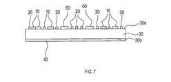
- FIG. 7 is a vertical sectional view taken along line VII-VII in FIG. 6.
- the reflection reducing device 50 includes a rectangular dielectric substrate 30.
- the dielectric substrate 30 includes a substrate front surface 30a and a substrate back surface 30b.
- the substrate front surface 30a and the substrate back surface 30b are used as a pattern forming layer.
- the direction of the first side of the dielectric substrate 30 is referred to as the x-axis direction
- the direction of the second side is referred to as the y-axis direction
- the normal direction of the substrate surface 30a is referred to as the z-axis direction.
- the reflection reducing device 50 includes a ground plane 40 provided on the substrate back surface 30b, and a first patch group and a second patch group provided on the substrate surface 30a.
- the ground plane 40 is a copper pattern formed so as to cover the entire surface of the substrate back surface 30b, and acts as a ground plane.
- the first patch group includes a plurality of first conductor patches 10.
- the plurality of first conductor patches 10 are parasitic patterns that are periodically and two-dimensionally arranged.
- the first conductor patch 10 is a copper pattern formed in a rectangular shape, and is arranged so that each side is inclined by 45 ° with respect to the x-axis.
- ⁇ direction the direction of the first side of the first conductor patch 10
- ⁇ direction the direction of the second side
- the ⁇ direction and the ⁇ direction are orthogonal to each other.
- the length L ⁇ 1 of the first conductor patch 10 in the ⁇ direction is different from the length L ⁇ 1 of the first conductor patch 10 in the ⁇ direction.
- Each of the plurality of first conductor patches 10 is insulated, is inclined at the same angle, and is arranged at equal intervals in the ⁇ direction and the ⁇ direction.
- the plurality of first conductor patches 10 are arranged as many as possible on the substrate surface 30a. That is, the space where the first conductor patch 10 is not disposed on the substrate surface 30a is a narrow space where the first conductor patch 10 cannot be disposed.
- the second patch group has a plurality of second conductor patches 20.
- the plurality of second conductor patches 20 include at least one first direction patch 20a and at least one second direction patch 20b.
- the first direction patch 20a is a linear copper pattern extending in the ⁇ direction.
- the second direction patch 20b is a linear copper pattern extending in the ⁇ direction.
- the length L ⁇ 2 of the first direction patch 20a is equal to the length L ⁇ 1 of the first conductor patch 10
- the length L ⁇ 2 of the second direction patch 20b is equal to the length L ⁇ 1 of the first conductor patch 10.
- the second patch group is provided on the substrate surface 30a at a position separated from the first patch group so as to follow the outer edge of the first patch group.
- the outer edge of the first patch group has a plurality of ⁇ -direction sides and a plurality of ⁇ -direction sides.
- the first direction patch 20a is disposed at a position away from the outer edge along the side in the ⁇ direction among the outer edges of the first patch group.
- the second direction patch 20b is disposed at a position spaced apart from the outer edge along the side in the ⁇ direction among the outer edges of the first patch group.
- the 1st direction patch 20a and the 2nd direction patch 20b are arrange
- first direction patches 20a or a plurality of second direction patches 20b may be arranged adjacent to each other along the same side of the outer edge of the first patch group.
- the first direction patch 20a and the second direction patch 20b are arranged as many as possible in the gap between the outer edge of the first patch group and the inner peripheral edge of the substrate surface 30a so as to be adjacent to each other. That is, since the first direction patch 20a and the second direction patch 20b have a smaller pattern than the first conductor patch 10, the first direction patch 20a and the second direction patch 20b are disposed so as to fill a narrow space where the first conductor patch 10 cannot be disposed.
- a radio wave arriving from the outside of the reflection reducing device 50 (hereinafter referred to as an incoming wave) has a horizontal polarization along the x direction. That is, the ⁇ direction and the ⁇ direction are inclined with respect to the polarization direction of the incoming wave.
- the incoming wave enters the reflection reducing device 50 the current excited by the incoming wave flows through the side in the ⁇ direction and the side in the ⁇ direction of the first conductor patch 10, and resonates in two directions, the ⁇ direction and the ⁇ direction.
- the resonance lengths in the two directions are different.
- the length L ⁇ 1 and the length L ⁇ 1 are set so that the phase difference ⁇ 1 between the reflection phase in the ⁇ direction and the reflection phase in the ⁇ direction of the first conductor patch 10 becomes 180 ° at a predetermined wavelength of the incoming wave.
- L ⁇ 1 is set. That is, the first conductor patch 10 has a shape that resonates in opposite phases in the ⁇ direction and the ⁇ direction.
- the lengths L ⁇ 1 and L ⁇ 2 at which the phase difference ⁇ 1 is 180 ° are calculated by simulation. Seeking and setting. Therefore, as shown in FIG.
- the polarization direction of the reflected wave changes from horizontal polarization of the incoming wave to vertical polarization along the y direction.
- the second conductor patch 20 since the length L ⁇ 2 of the first direction patch 20a is equal to the length ⁇ 1 and the length L ⁇ 2 of the second direction patch 20b is equal to the length L ⁇ 1, the second conductor patch 20 has a reflection phase of the first direction patch 20a. And the phase difference ⁇ 2 between the reflection phase of the second direction patch 20b is 180 °. Therefore, the second conductor patch 20 converts the polarization direction of the reflected wave into vertical polarization along the y direction by the pair of the adjacent first direction patch 20a and second direction patch 20b.
- the polarization conversion effect by the single first conductor patch 10 is not sufficient, and the entire plurality of first conductor patches 10 arranged periodically exhibits the polarization conversion effect. Therefore, when the second patch group is not arranged on the substrate surface 30a, the periodic arrangement is interrupted at the outer edge portion of the first patch group, so that a sufficient polarization conversion effect is not exhibited.
- the small 1st direction patch 20a and the 2nd direction patch 20b are arrange
- the reflection reducing device 50 when the first patch group is removed and the second conductor patch 20 is disposed in the portion where the first conductor patch 10 is disposed, the first conductor patch 10 is disposed.
- the gap between patches increases and the polarization conversion effect decreases. Therefore, after arranging as many first conductor patches 10 as possible on the substrate surface 30a, as many second conductor patches 20 as possible are arranged in the gap between the outer edge of the first patch group and the inner periphery of the substrate surface 30a. It is desirable.
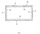
- FIG. 5 shows an anechoic chamber 350 as one application example of the reflection reducing device 50.
- an anechoic chamber is a room in which a radio wave absorber is stretched on the inner surface such as a ceiling or a side wall so that a radio wave generated inside is not reflected.
- the reflection reducing device 50 is stretched on the inner surface such as the ceiling and the side wall, and the radio wave absorber 300 is stretched on the reflection reducing device 50.
- the radio wave generated inside and incident on the inner surface thereof is absorbed by the radio wave absorber 300.
- the anechoic chamber 350 can further suppress the influence of the reflection of the radio wave generated inside, compared with the anechoic chamber in which the reflection reducing device 50 is not stretched on the inner surface.
- the first conductor patch 10 has a pattern shape that resonates on two sides in the ⁇ direction and the ⁇ direction and has different resonance lengths in the two directions. Therefore, since a phase difference occurs between the reflection phase in the ⁇ direction and the reflection phase in the ⁇ direction of the first conductor patch 10, the polarization direction of the reflected wave generated by reflecting the incoming wave by the first patch group is the incoming wave. Is converted to a direction different from the polarization direction.
- the second conductor patch 20 converts the polarization direction of the reflected wave into a direction different from the polarization direction of the incoming wave by a combination of the first direction patch 20a and the second direction patch 20b.
- the first direction patch 20a and the second direction patch 20b each have a pattern shape that resonates only in one direction, and is smaller than the first conductor patch 10 that resonates in two directions. Therefore, the first direction patch 20a and the second direction patch 20b can be arranged in a narrow space where the first conductor patch 10 cannot be arranged. That is, the first direction patch 20a and the second direction patch 20b can be arranged outside the first patch group having no space for arranging the first conductor patch 10. Thereby, compared with the case where only the 1st conductor patch 10 is arrange
- the ⁇ direction and the ⁇ direction are orthogonal to each other.
- the first conductor patch 10 has a shape that resonates in opposite phases in the ⁇ direction and the ⁇ direction. Therefore, the first conductor patch 10 can rotate the polarization direction of the reflected wave by 90 ° from the polarization direction of the incoming wave. Further, since the first direction patch 20a and the second direction patch 20b included in the second conductor patch 20 resonate in opposite phases, the second conductor patch 20 includes the first direction patch 20a and the second direction patch 20b. With this combination, the polarization direction of the reflected wave can be rotated by 90 ° from the polarization direction of the incoming wave.
- the plurality of first conductor patches 10 as a whole differ in the polarization direction of the reflected wave from the polarization direction of the incoming wave. Can be converted into directions.
- the adjacent first direction patch 20a and the second direction patch 20b act integrally and reflect.
- the polarization direction of the wave can be converted to a direction different from the polarization direction of the incoming wave.
- the reflection reduction device 150 according to the second embodiment is different from the reflection reduction device 50 according to the first embodiment in that an antenna unit 60 is provided.
- an antenna unit 60 is provided.
- the substrate surface 30 a of the reflection reducing device 150 includes a first patch group including a plurality of first conductor patches 10 and a second patch group including a plurality of second conductor patches 20.
- at least one antenna unit 60 is provided.
- the antenna unit 60 includes a plurality of patch antennas 60 a and a plurality of feeder lines 60 b.
- the radiated wave radiated from the antenna unit 60 has horizontal polarization along the x direction.
- the 1st conductor patch 10 is arrange
- the first direction patch 20a is disposed along the ⁇ direction
- the second direction patch 20b is disposed along the ⁇ direction.
- the second patch group is set in the vicinity of the antenna portion 60 and the inner peripheral edge portion of the substrate surface 30a.
- the first patch group is installed on the portion of the substrate surface 30a excluding the antenna portion 60, the vicinity of the antenna portion 60, and the inner peripheral edge portion of the substrate surface 30a.
- the reflection reducing device 150 as many first conductor patches 10 as possible are arranged so as to surround the antenna unit 60 formed on the substrate surface 30a. Then, in the gap between the outer edge of the first conductor patch 10 and the antenna unit 60 and the gap between the outer edge of the first conductor patch 10 and the inner periphery of the substrate surface 30a, the first direction patch 20a and the second direction patch 20b are provided. Has been placed.
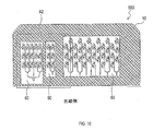
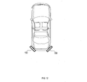
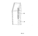
- the reflection reducing device 150 an object exists in the radiation direction of the antenna unit 60, and a part of the radiated wave radiated from the antenna unit 60 is reflected by the object and becomes an incoming wave arriving at the antenna unit 60. It is assumed that it will be installed in a place. Specifically, for example, as shown in FIGS. 12 and 13, it is assumed that the reflection reducing device 150 is mounted inside the bumper 80 of the vehicle.
- the reflection reducing device 150 When the reflection reducing device 150 is mounted inside the bumper 80, a part of the radiated wave radiated from the antenna unit 60 of the reflection reducing device 150 is transmitted through the bumper 80, and a part is reflected by the bumper 80 and reflected.
- the incoming wave arrives at the reduction device 150.
- the incoming wave is re-reflected by the reflection reducing device 150. If the reflected wave generated by re-reflection and the radiated wave interfere with each other, the radiated wave may be attenuated.
- the polarized wave of the reflected wave generated by re-reflection by the reflection reducing device 150 is rotated by 90 ° from the horizontal polarization of the radiated wave. Accordingly, the polarization component of the reflected wave has a relatively large vertical polarization component and a relatively small horizontal polarization component, so that interference between the reflected wave and the radiated wave is suppressed.
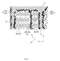
- the structure of the reflection reducing device 550 of the comparative example is shown in FIGS.
- the antenna unit 60 and the first patch group are arranged on the substrate surface 30a, and the second patch group is not arranged.
- the first conductor patch 10 since the first conductor patch 10 cannot be disposed as it is in the vicinity of the antenna unit 60 and the inner peripheral edge portion of the substrate surface 30a, the first conductor patch 10 is disposed in a small cut.
- the first conductor patch 10 disposed in the vicinity of the antenna unit 60 and the inner peripheral edge portion of the substrate surface 30a has a side length in the ⁇ direction shorter than the length L ⁇ 1, Since the length is shorter than the length L ⁇ 1, it does not function as a polarization conversion unit.
- the part functioning as the polarization converting part is an area R excluding the vicinity of the antenna part 60 and the inner peripheral part of the substrate 30a in the installation area of the first conductor patch 10. Only. Therefore, the reflection reducing device 550 exhibits a lower polarization conversion effect than the reflection reducing device 150.
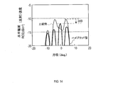
- FIG. 14 shows a simulation result of the intensity of the horizontally polarized component of the reflected wave when the reflection reducing device 150 and the reflection reducing device 550 are respectively installed in the bumper 80 and the horizontally polarized radiation is radiated from the antenna unit 60. Indicates.
- the reflection intensity of the horizontal polarization component is reduced by 2 dB as compared with the reflection reducing device 550. Therefore, the reflection reducing device 150 can suppress interference between the radiated wave and the reflected wave more than the reflection reducing device 550.
- the first direction patch 20a and the second direction patch that are smaller than the first conductor patch 10 are provided in the vicinity of the antenna unit 60 and the inner peripheral edge portion of the substrate surface 30a where there is no space for arranging the first conductor patch 10. 20b is arranged. Thereby, compared with the case where only the 1st conductor patch 10 is arrange
- the first conductor patch 10, the first direction patch 20a, and the second direction patch 20b are arranged so as to be inclined by 45 ° with respect to the polarization direction of the incoming wave, but the inclination angle is 45. It is not limited to °.
- the reflection reducing devices 50 and 150 exhibit the highest polarization conversion effect when the inclination angle is set to 45 °.
- the ⁇ direction and the ⁇ direction are set to 35 ° to 55 ° with respect to the polarization direction of the incoming wave. Even when tilted within the range of °, the polarization conversion effect is exhibited.
- the phase difference between the reflection phase in the ⁇ direction and the reflection phase in the ⁇ direction is set to 180 °, but the phase difference is not limited to 180 ° and is more than 0 °. A large phase difference is sufficient.
- the reflection reducing devices 50 and 150 only need to rotate and reflect the polarization direction of the incoming wave even if it is less than 90 °. If there is a difference between the polarization directions of the reflected wave and the incoming wave, the influence of the reflected wave can be suppressed.
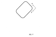
- the first conductor patch 10 has a rectangular shape, but the shape of the first conductor patch 10 is not limited to a rectangular shape.
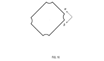
- the first conductor patch 10 has a pattern shape in which a triangle or a quarter circular cutout is formed at four ends of two diagonal lines. May be.
- two sides sandwiching the notch are an ⁇ side and a ⁇ direction side.
- the first conductor patch 10 may have a pattern shape in which four ends of two diagonal lines are formed in a round shape.
- two sides sandwiching a round end are a side in the ⁇ direction and a side in the ⁇ direction.
- the first conductor patch 10 may have a pattern shape in which two linear patterns intersect.
- two linear patterns are an ⁇ -direction side and a ⁇ -direction side, respectively.
- the first conductor patch 10 may have a pattern shape in which two linear patterns intersect and the center portion is cut off.
- the two linear patterns are a side in the ⁇ direction and a side in the ⁇ direction, respectively.
- the first conductor patch 10 may have a rhombus pattern shape.
- the first conductor patch 10 shown in FIG. 20 resonates at three sides in the ⁇ direction, ⁇ direction, and ⁇ direction.
- the lengths of the sides in the three directions may be set so that the polarization direction of the reflected wave obtained by combining the reflection components in the three directions rotates from the polarization direction of the incoming wave.
- the second conductor patch 20 includes a linear pattern that resonates only in the ⁇ direction, a linear pattern that resonates only in the ⁇ direction, and a linear pattern that resonates only in the ⁇ direction.
- the first conductor patch 10 may have an axisymmetric octagonal pattern shape.
- the first conductor patch 10 shown in FIG. 21 resonates at four sides in the ⁇ direction, ⁇ direction, ⁇ direction, and ⁇ direction.
- the length of the sides in the four directions may be set so that the polarization direction of the reflected wave obtained by combining the reflection components in the four directions rotates from the polarization direction of the incoming wave.
- the second conductor patch 20 includes a linear pattern that resonates only in the ⁇ direction, a linear pattern that resonates only in the ⁇ direction, a linear pattern that resonates only in the ⁇ direction, and a ⁇ direction. And a linear pattern that resonates.
- a plurality of functions of one constituent element in the above embodiment may be realized by a plurality of constituent elements, or a single function of one constituent element may be realized by a plurality of constituent elements. . Further, a plurality of functions possessed by a plurality of constituent elements may be realized by one constituent element, or one function realized by a plurality of constituent elements may be realized by one constituent element. Moreover, you may abbreviate
Landscapes
- Engineering & Computer Science (AREA)
- Computer Security & Cryptography (AREA)
- Radar, Positioning & Navigation (AREA)
- Remote Sensing (AREA)
- Aerials With Secondary Devices (AREA)
- Waveguide Aerials (AREA)
Priority Applications (2)
| Application Number | Priority Date | Filing Date | Title |
|---|---|---|---|
| CN201980021909.6A CN111903001B (zh) | 2018-04-05 | 2019-04-03 | 反射降低装置 |
| US17/038,625 US11336024B2 (en) | 2018-04-05 | 2020-09-30 | Reflection reducing apparatus |
Applications Claiming Priority (2)
| Application Number | Priority Date | Filing Date | Title |
|---|---|---|---|
| JP2018073054A JP6970051B2 (ja) | 2018-04-05 | 2018-04-05 | 反射低減装置 |
| JP2018-073054 | 2018-04-05 |
Related Child Applications (1)
| Application Number | Title | Priority Date | Filing Date |
|---|---|---|---|
| US17/038,625 Continuation US11336024B2 (en) | 2018-04-05 | 2020-09-30 | Reflection reducing apparatus |
Publications (1)
| Publication Number | Publication Date |
|---|---|
| WO2019194234A1 true WO2019194234A1 (ja) | 2019-10-10 |
Family
ID=68100442
Family Applications (1)
| Application Number | Title | Priority Date | Filing Date |
|---|---|---|---|
| PCT/JP2019/014841 Ceased WO2019194234A1 (ja) | 2018-04-05 | 2019-04-03 | 反射低減装置 |
Country Status (4)
| Country | Link |
|---|---|
| US (1) | US11336024B2 (cg-RX-API-DMAC7.html) |
| JP (1) | JP6970051B2 (cg-RX-API-DMAC7.html) |
| CN (1) | CN111903001B (cg-RX-API-DMAC7.html) |
| WO (1) | WO2019194234A1 (cg-RX-API-DMAC7.html) |
Families Citing this family (4)
| Publication number | Priority date | Publication date | Assignee | Title |
|---|---|---|---|---|
| JP2023509575A (ja) * | 2020-01-08 | 2023-03-09 | メタウェーブ コーポレーション | 2次元ビームスキャニングを有するリフレクトアレイアンテナ |
| TWI789877B (zh) * | 2021-08-19 | 2023-01-11 | 特崴光波導股份有限公司 | 天線結構 |
| JP7789797B2 (ja) | 2021-10-29 | 2025-12-22 | 日本たばこ産業株式会社 | 吸引装置、基材、及び制御方法 |
| CN116234278B (zh) * | 2021-12-06 | 2025-07-11 | 苏州大学 | 电磁波吸收材料、装置及波导器件 |
Citations (2)
| Publication number | Priority date | Publication date | Assignee | Title |
|---|---|---|---|---|
| US20090079645A1 (en) * | 2007-09-26 | 2009-03-26 | Michael John Sotelo | Low Loss, Variable Phase Reflect Array |
| WO2017175835A1 (ja) * | 2016-04-06 | 2017-10-12 | 株式会社デンソー | アンテナ装置 |
Family Cites Families (9)
| Publication number | Priority date | Publication date | Assignee | Title |
|---|---|---|---|---|
| JP3902192B2 (ja) * | 2004-04-08 | 2007-04-04 | 英一 小川 | 電波偏波変換共振反射器、電波偏波変換共振反射装置、無線通信システム、金属対応無線icタグ装置、物品及びrfidシステム |
| JP2009005184A (ja) * | 2007-06-22 | 2009-01-08 | Suncall Corp | パッチアンテナ及びrfidインレット |
| JP5603907B2 (ja) | 2012-08-27 | 2014-10-08 | 株式会社Nttドコモ | リフレクトアレー |
| EP2905840B1 (en) * | 2012-10-01 | 2018-08-01 | NTT DoCoMo, Inc. | Reflect array |
| JP6282469B2 (ja) * | 2014-01-21 | 2018-02-21 | 日本電業工作株式会社 | アンテナ |
| CN105206940B (zh) * | 2014-06-30 | 2018-12-14 | 南京理工大学 | 基于人工磁导体的低剖面极化扭转反射板 |
| WO2017104754A1 (ja) * | 2015-12-15 | 2017-06-22 | 株式会社日本自動車部品総合研究所 | アンテナ装置 |
| DE102015225578A1 (de) * | 2015-12-17 | 2017-06-22 | Robert Bosch Gmbh | Vorrichtung zum Empfangen von Mikrowellenstrahlung |
| KR101766216B1 (ko) * | 2016-02-05 | 2017-08-09 | 한국과학기술원 | 인공 자기 도체를 이용한 배열 안테나 |
-
2018
- 2018-04-05 JP JP2018073054A patent/JP6970051B2/ja active Active
-
2019
- 2019-04-03 CN CN201980021909.6A patent/CN111903001B/zh active Active
- 2019-04-03 WO PCT/JP2019/014841 patent/WO2019194234A1/ja not_active Ceased
-
2020
- 2020-09-30 US US17/038,625 patent/US11336024B2/en active Active
Patent Citations (2)
| Publication number | Priority date | Publication date | Assignee | Title |
|---|---|---|---|---|
| US20090079645A1 (en) * | 2007-09-26 | 2009-03-26 | Michael John Sotelo | Low Loss, Variable Phase Reflect Array |
| WO2017175835A1 (ja) * | 2016-04-06 | 2017-10-12 | 株式会社デンソー | アンテナ装置 |
Also Published As
| Publication number | Publication date |
|---|---|
| JP6970051B2 (ja) | 2021-11-24 |
| JP2019186668A (ja) | 2019-10-24 |
| US11336024B2 (en) | 2022-05-17 |
| CN111903001A (zh) | 2020-11-06 |
| CN111903001B (zh) | 2022-06-28 |
| US20210028551A1 (en) | 2021-01-28 |
Similar Documents
| Publication | Publication Date | Title |
|---|---|---|
| WO2019194234A1 (ja) | 反射低減装置 | |
| JP7339207B2 (ja) | メタサーフェス反射板アレイ | |
| JP6499116B2 (ja) | アンテナ装置 | |
| CN107017456B (zh) | 接收微波射线的设备 | |
| US11121461B2 (en) | Antenna device | |
| CN109302851B (zh) | 一种反射阵天线及通信设备 | |
| WO2017146164A1 (ja) | アンテナ装置 | |
| JP6282469B2 (ja) | アンテナ | |
| JP6510394B2 (ja) | アンテナ装置 | |
| JP6008081B2 (ja) | アレーアンテナ装置 | |
| JP6705784B2 (ja) | アンテナ装置 | |
| CN105006659B (zh) | 两个双反射面天线的阵列和包括该阵列的卫星 | |
| JP7664747B2 (ja) | 電波吸収素子および集合体 | |
| WO2018198970A1 (ja) | アンテナ装置 | |
| JPS5915521B2 (ja) | 円偏波アレイアンテナ | |
| JP2013070366A (ja) | 空中線 | |
| JP2020162052A (ja) | アンテナ装置および反射位相制御方法 | |
| EP4664678A1 (en) | Radar sensor | |
| JP7795633B2 (ja) | 電波制御装置および通信システム | |
| JP2013093710A (ja) | アンテナ装置 | |
| JP7311078B1 (ja) | アンテナ装置 | |
| JP2015185988A (ja) | アンテナ装置 | |
| JP6433567B2 (ja) | 送受信アンテナ、スリットの設計方法 | |
| JP2005086528A (ja) | 電波受信アンテナ用の妨害波シールド構造物 | |
| TW202527653A (zh) | 雜訊去除體 |
Legal Events
| Date | Code | Title | Description |
|---|---|---|---|
| 121 | Ep: the epo has been informed by wipo that ep was designated in this application |
Ref document number: 19780529 Country of ref document: EP Kind code of ref document: A1 |
|
| NENP | Non-entry into the national phase |
Ref country code: DE |
|
| 122 | Ep: pct application non-entry in european phase |
Ref document number: 19780529 Country of ref document: EP Kind code of ref document: A1 |